JP2006520089A - Method and system for manufacturing a multilayer device on a substrate - Google Patents
Method and system for manufacturing a multilayer device on a substrate Download PDFInfo
- Publication number
- JP2006520089A JP2006520089A JP2005500831A JP2005500831A JP2006520089A JP 2006520089 A JP2006520089 A JP 2006520089A JP 2005500831 A JP2005500831 A JP 2005500831A JP 2005500831 A JP2005500831 A JP 2005500831A JP 2006520089 A JP2006520089 A JP 2006520089A
- Authority
- JP
- Japan
- Prior art keywords
- layer
- semiconductor layer
- bonded
- substrate
- layers
- Prior art date
- Legal status (The legal status is an assumption and is not a legal conclusion. Google has not performed a legal analysis and makes no representation as to the accuracy of the status listed.)
- Withdrawn
Links
Images


Classifications
-
- H—ELECTRICITY
- H01—ELECTRIC ELEMENTS
- H01L—SEMICONDUCTOR DEVICES NOT COVERED BY CLASS H10
- H01L22/00—Testing or measuring during manufacture or treatment; Reliability measurements, i.e. testing of parts without further processing to modify the parts as such; Structural arrangements therefor
- H01L22/20—Sequence of activities consisting of a plurality of measurements, corrections, marking or sorting steps
-
- H—ELECTRICITY
- H01—ELECTRIC ELEMENTS
- H01L—SEMICONDUCTOR DEVICES NOT COVERED BY CLASS H10
- H01L21/00—Processes or apparatus adapted for the manufacture or treatment of semiconductor or solid state devices or of parts thereof
- H01L21/02—Manufacture or treatment of semiconductor devices or of parts thereof
- H01L21/04—Manufacture or treatment of semiconductor devices or of parts thereof the devices having at least one potential-jump barrier or surface barrier, e.g. PN junction, depletion layer or carrier concentration layer
- H01L21/18—Manufacture or treatment of semiconductor devices or of parts thereof the devices having at least one potential-jump barrier or surface barrier, e.g. PN junction, depletion layer or carrier concentration layer the devices having semiconductor bodies comprising elements of Group IV of the Periodic System or AIIIBV compounds with or without impurities, e.g. doping materials
- H01L21/30—Treatment of semiconductor bodies using processes or apparatus not provided for in groups H01L21/20 - H01L21/26
-
- B—PERFORMING OPERATIONS; TRANSPORTING
- B81—MICROSTRUCTURAL TECHNOLOGY
- B81C—PROCESSES OR APPARATUS SPECIALLY ADAPTED FOR THE MANUFACTURE OR TREATMENT OF MICROSTRUCTURAL DEVICES OR SYSTEMS
- B81C99/00—Subject matter not provided for in other groups of this subclass
- B81C99/0035—Testing
- B81C99/0045—End test of the packaged device
-
- H—ELECTRICITY
- H01—ELECTRIC ELEMENTS
- H01L—SEMICONDUCTOR DEVICES NOT COVERED BY CLASS H10
- H01L22/00—Testing or measuring during manufacture or treatment; Reliability measurements, i.e. testing of parts without further processing to modify the parts as such; Structural arrangements therefor
- H01L22/10—Measuring as part of the manufacturing process
- H01L22/14—Measuring as part of the manufacturing process for electrical parameters, e.g. resistance, deep-levels, CV, diffusions by electrical means
-
- H—ELECTRICITY
- H01—ELECTRIC ELEMENTS
- H01L—SEMICONDUCTOR DEVICES NOT COVERED BY CLASS H10
- H01L2224/00—Indexing scheme for arrangements for connecting or disconnecting semiconductor or solid-state bodies and methods related thereto as covered by H01L24/00
- H01L2224/01—Means for bonding being attached to, or being formed on, the surface to be connected, e.g. chip-to-package, die-attach, "first-level" interconnects; Manufacturing methods related thereto
- H01L2224/10—Bump connectors; Manufacturing methods related thereto
- H01L2224/12—Structure, shape, material or disposition of the bump connectors prior to the connecting process
- H01L2224/13—Structure, shape, material or disposition of the bump connectors prior to the connecting process of an individual bump connector
-
- H—ELECTRICITY
- H01—ELECTRIC ELEMENTS
- H01L—SEMICONDUCTOR DEVICES NOT COVERED BY CLASS H10
- H01L2224/00—Indexing scheme for arrangements for connecting or disconnecting semiconductor or solid-state bodies and methods related thereto as covered by H01L24/00
- H01L2224/01—Means for bonding being attached to, or being formed on, the surface to be connected, e.g. chip-to-package, die-attach, "first-level" interconnects; Manufacturing methods related thereto
- H01L2224/10—Bump connectors; Manufacturing methods related thereto
- H01L2224/15—Structure, shape, material or disposition of the bump connectors after the connecting process
- H01L2224/16—Structure, shape, material or disposition of the bump connectors after the connecting process of an individual bump connector
-
- H—ELECTRICITY
- H01—ELECTRIC ELEMENTS
- H01L—SEMICONDUCTOR DEVICES NOT COVERED BY CLASS H10
- H01L2924/00—Indexing scheme for arrangements or methods for connecting or disconnecting semiconductor or solid-state bodies as covered by H01L24/00
- H01L2924/013—Alloys
- H01L2924/014—Solder alloys
-
- H—ELECTRICITY
- H01—ELECTRIC ELEMENTS
- H01L—SEMICONDUCTOR DEVICES NOT COVERED BY CLASS H10
- H01L2924/00—Indexing scheme for arrangements or methods for connecting or disconnecting semiconductor or solid-state bodies as covered by H01L24/00
- H01L2924/10—Details of semiconductor or other solid state devices to be connected
- H01L2924/11—Device type
- H01L2924/13—Discrete devices, e.g. 3 terminal devices
- H01L2924/1304—Transistor
- H01L2924/1305—Bipolar Junction Transistor [BJT]
-
- H—ELECTRICITY
- H01—ELECTRIC ELEMENTS
- H01L—SEMICONDUCTOR DEVICES NOT COVERED BY CLASS H10
- H01L2924/00—Indexing scheme for arrangements or methods for connecting or disconnecting semiconductor or solid-state bodies as covered by H01L24/00
- H01L2924/10—Details of semiconductor or other solid state devices to be connected
- H01L2924/11—Device type
- H01L2924/13—Discrete devices, e.g. 3 terminal devices
- H01L2924/1304—Transistor
- H01L2924/1306—Field-effect transistor [FET]
- H01L2924/13091—Metal-Oxide-Semiconductor Field-Effect Transistor [MOSFET]
Landscapes
- Engineering & Computer Science (AREA)
- Microelectronics & Electronic Packaging (AREA)
- Manufacturing & Machinery (AREA)
- Computer Hardware Design (AREA)
- Power Engineering (AREA)
- Physics & Mathematics (AREA)
- Condensed Matter Physics & Semiconductors (AREA)
- General Physics & Mathematics (AREA)
- Micromachines (AREA)
- Semiconductor Integrated Circuits (AREA)
- Element Separation (AREA)
Abstract
バルク性基板上に多層能動素子を製造する方法が開示される。多層微小電気機械および微小流体素子は、素子の分解された層がある または、弱い結合領域上の所定の弱いおよび強い結合領域の層を有する基板に製造される。所定の弱いおよび強い結合領域の層を有する基板に製造される多層集積回路が開示される。任意の数の層は、基板上に所定の素子を作成するため、結合され、スタックされることができる。また、層とその装置の上との間の相互接続を形成するため、エッジ相互接続を作成する方法および基板を通じたバイアが開示される。A method of manufacturing a multilayer active device on a bulk substrate is disclosed. Multilayer microelectromechanical and microfluidic devices are fabricated into substrates that have a decomposed layer of devices or have a layer of predetermined weak and strong bonding regions on weak bonding regions. A multilayer integrated circuit manufactured on a substrate having a layer of predetermined weak and strong coupling regions is disclosed. Any number of layers can be combined and stacked to create a given device on the substrate. Also disclosed are methods of creating edge interconnects and vias through a substrate to form an interconnect between a layer and the top of the device.
Description
関連出願の相互参照
本出願は、米国特許法119(e)の下で、本願明細書において参照されたものとする2002年11月20日に出願の暫定的な米国出願番号第60/428,125号の利益を請求する。
CROSS-REFERENCE TO RELATED APPLICATIONS This application, under U.S.C. 119 (e), provisional U.S. Application Serial No. filed November 20, 2002 to those referenced herein No. 60/428, Claim the profit of 125.
この発明は、基板上に多層能動素子を製造するための方法およびシステムに関し、特に、基板上の垂直の集積回路、微小電気機械装置、および、微小流体素子の製造に関する。 The present invention relates to methods and systems for manufacturing multilayer active devices on a substrate, and more particularly to the manufacture of vertical integrated circuits, microelectromechanical devices, and microfluidic devices on a substrate.
より高速かつより安価な集積回路の需要は、ますます増大している。ムーアの法則は、平方インチごとのトランジスタの数は毎年2倍になると断定する。しかしながら、従来の二次元の(または平らな)チップ製造方法がその限界に達しているので、ムーアの法則の予言を成し遂げるために、チップ製造の新領域を広げるためのより革新的な技術が必要である。 The demand for faster and cheaper integrated circuits is increasing. Moore's Law concludes that the number of transistors per square inch doubles every year. However, as traditional two-dimensional (or flat) chip manufacturing methods have reached their limits, more innovative techniques are needed to expand new areas of chip manufacturing in order to achieve Moore's Law prophecy. It is.
これまで、より密度の高い集積回路を求める大部分の要求は、比較的平らな構造上に製造される縮小する能動素子によって応じられた。すなわち、二次元のチップ製造は半導体製造の支配的な方法であった。大部分の半導体(訳注*1)素子は、平らは単結晶の半導体基板において造られてきた。 In the past, most demands for denser integrated circuits have been met by shrinking active devices fabricated on relatively flat structures. That is, two-dimensional chip manufacturing has been the dominant method of semiconductor manufacturing. Most semiconductor devices have been fabricated on flat, single crystal semiconductor substrates.
この方法は、第三次元への非常に制限された垂直の集積化のみを許容する。
二次元のチップ製造の限界が近づいているので、性能における大きな進展は、三次元のチップ製造(すなわちZ次元のチップ製造)から派生する。
This method only allows very limited vertical integration into the third dimension.
As the limits of two-dimensional chip manufacturing are approaching, significant advances in performance are derived from three-dimensional chip manufacturing (ie, Z-dimensional chip manufacturing).
同じパッケージへのマイクロデバイスの垂直統合またはスタッキングは、荷造り量を減少させる、回路密度を増加させかつ基盤スペースを節約する、性能および機能を増加させるための魅力的な方法である。内部チップ遅延および消費電力の減少は、両方ともスタックされた集積における利益である。素子が薄くなりかつ互いの上に積み重なる場合、費用および回路密度における利点は潜在的に莫大である。集積回路および微小電気機械のプロセスのため、シリコン・ウェーハの第三次元は、主に未開発のままである。 Vertical integration or stacking of microdevices into the same package is an attractive way to increase performance and functionality, reduce packing, increase circuit density and save board space. Internal chip delay and reduced power consumption are both benefits in stacked integration. When devices are thinned and stacked on top of each other, the advantages in cost and circuit density are potentially enormous. Due to integrated circuit and microelectromechanical processes, the third dimension of silicon wafers remains largely undeveloped.
二次元の装置の垂直のスタッキングへの現行の商用アプローチは、概してチップ・スケールであって、研磨によるウェーハの薄層化に依存する。大部分の方法は、貫通孔を通じたまたはワイヤ接着の積み重なったマザー‐ドウターチップの相互接続に依存する。
現行の方法はすべて、パッケージ・サイズ、費用、信頼性およびイールド・インパクトに関して限界を有する。前記の問題点にもかかわらず、三次元集積化を達成するスタッキング装置は、微小電気機械システム「MEMS」と特定用途向けIC「ASIC」コントローラとの結合において特に、応用対象を見つけている。個々のチップのスタッキングにより作成される高密度メモリー・パッケージは、専門の応用対象を見つけた。
Current commercial approaches to vertical stacking of two-dimensional devices are generally chip scale and rely on wafer thinning by polishing. Most methods rely on mother-daughter chip interconnections through through holes or stacked with wire bonds.
All current methods have limitations with respect to package size, cost, reliability and yield impact. Despite the above-mentioned problems, stacking devices that achieve three-dimensional integration are finding particular application in combining microelectromechanical systems “MEMS” and application specific IC “ASIC” controllers. High-density memory packages created by stacking individual chips have found specialized applications.
IBMの米国特許NO.6,355,501は、三次元集積回路アセンブリ、概してオンチップ・スケールを製造する方法を開示する。その中に開示されているのは、三次元のスタックされたシリコンオンインシュレータ「SOI」チップからなるアセンブリ、およびこのような集積回路アセンブリを形成する方法である。SOIチップの各々は、半導体デバイスに電気的な接触させる第1のメタライゼーション・パターンへ機械的な接触をさせるハンドラを含む。金属化パターン(訳注*2)は、順番に、半導体デバイスの対向する表面上に配置される第2のメタライゼーション・パターンに接触する。 IBM US Pat. US 6,355,501 discloses a method of manufacturing a three-dimensional integrated circuit assembly, generally an on-chip scale. Disclosed therein is an assembly consisting of a three-dimensional stacked silicon-on-insulator “SOI” chip and a method of forming such an integrated circuit assembly. Each of the SOI chips includes a handler that provides mechanical contact to a first metallization pattern that provides electrical contact to the semiconductor device. The metallization pattern in turn contacts a second metallization pattern disposed on the opposing surface of the semiconductor device.
開示された方法は、以下のステップを含む:
a)基板の第1の表面上に第3の金属化パターンを有する基板の提供;b)SOIチップの第2のメタライゼーション・パターンを基板の第3の金属化パターンと電気接触させることによる、基板の第1の表面上へのSOIチップのうちの1つの整列配置;c)SOIチップからのハンドラの除去、および、SOIチップの第1のメタライゼーション・パターンの露出;d)第1のSOIチップの露出された第1のメタライゼーション・パターンを第2のSOIチップの第2のメタライゼーション・パターンと電気接触させることによる、第2のSOIチップの1つの第1のSOIチップとの整列配置;およびe)他方の上に以降のSOIチップを取付けるため、ステップc)およびd)の繰返し。
The disclosed method includes the following steps:
a) providing a substrate having a third metallization pattern on the first surface of the substrate; b) electrically contacting the second metallization pattern of the SOI chip with the third metallization pattern of the substrate; Alignment of one of the SOI chips on the first surface of the substrate; c) removal of the handler from the SOI chip and exposure of the first metallization pattern of the SOI chip; d) the first SOI Alignment of the second SOI chip with one first SOI chip by electrically contacting the exposed first metallization pattern of the chip with the second metallization pattern of the second SOI chip And e) repeating steps c) and d) to mount a subsequent SOI chip on the other.
しかしながら、この参照は、極端に高価でかつ別々に機能上制限されるかもしれない方法を教示する。 However, this reference teaches a method that is extremely expensive and may be separately functionally limited.
上述した米国特許NO.6,335,501において教示される方法の主要な不都合は、その出願人は、三次元回路をウェーハ・スケール上に形成することは低イールドにつながることを強調していることである。さらに、各々のチップの整列は、ウェーハ・スケールのスタッキングを妨げる本質的な問題であると考えられる。各々のチップのスタッキングステップは、互いに結合される層の整列を含む。透明な接着材、および、ウィンドウは、互いに結合される両方の表面上の整列マークへの光学アクセスを可能にするために提供されなければならない。 The aforementioned U.S. Pat. A major disadvantage of the method taught in US Pat. No. 6,335,501 is that the applicant emphasizes that forming a three-dimensional circuit on a wafer scale leads to low yield. Furthermore, the alignment of each chip is considered to be an essential problem that prevents wafer scale stacking. Each chip stacking step includes an alignment of layers bonded together. Transparent adhesive and windows must be provided to allow optical access to alignment marks on both surfaces that are bonded together.
さらに、ハンドラは整列マークに透過的でなければならない。他の不都合は、連続して起こる繰返されたプロセスのステップの数に関する。その中に記載されたように、スタックされた層の間で電気接触(訳注*3)させるため、それがスタックされ、かつ、整列配置される場合、ハンダ・リフロー・ステップが各々の層の間で実行される。リフローの後、チップ・スタックは、端で結合される。その上、ハンドラは、(レーザーまたは他の加熱によって)接着剤除去剤により除去され、研磨されなければならず、次の層の前の他の準備ステップは、結合されることができる。最後に、過剰基板は、研磨される、または、それでなければ除去のためエッチバックされる。 In addition, the handler must be transparent to the alignment mark. Another disadvantage relates to the number of repeated process steps that occur in succession. As described therein, a solder reflow step is performed between each layer when it is stacked and aligned to make electrical contact between the stacked layers. Is executed. After reflow, the chip stack is bonded at the end. Moreover, the handler must be removed with an adhesive remover (by laser or other heating) and polished, and other preparatory steps before the next layer can be combined. Finally, the excess substrate is polished or otherwise etched back for removal.
これらの欠点は、費用および機能に関連したいくつかの不都合を導く。費用損失は、研磨削除;多数の連続して起こるステップ;ウェーハ・スケールスタッキングに対するチップ・スケール。ここにおいて、ウェーハ・スケールは費用を減少させることは公知である;ウェーハ・スケール上に発生するイールドを克服の不可能性、したがってチップ・スケールへの逆戻り;層の数の限定、したがって、より高い数のスタックを形成するため、スタックは、他のスタッキングの上に積み重ならなければならない;連続して起こる統計学的に依存している数は相互接続によるので、全体のイールドは減少する;多数のリフロー・ステップは、潜在的に他の層にダメージを与える;点について見出される。機能上の欠点は、診断の欠如;相互接続汎用性の欠如;相互接続のための限られたスペース;大きいスタック(特にメモリー・スタック)の限られたアドレス指定能力;ノイズ・シールドを集積化する能力の欠如;熱散逸を集積化する能力の欠如;接地面の能力の欠如;層の数の限定;を含む。 These shortcomings lead to several disadvantages related to cost and function. Cost loss is polishing removal; multiple consecutive steps; chip scale versus wafer scale stacking. Here, the wafer scale is known to reduce costs; the inability to overcome the yield generated on the wafer scale, and thus back to the chip scale; the limited number of layers, and therefore higher In order to form a stack of numbers, the stack must be stacked on top of other stacking; the overall statistical yield is reduced because consecutive statistically dependent numbers are interconnected; Numerous reflow steps potentially damage other layers; found for points. Functional disadvantages include lack of diagnostics; lack of interconnect versatility; limited space for interconnects; limited addressability of large stacks (especially memory stacks); integrate noise shield Lack of ability; lack of ability to integrate heat dissipation; lack of ground plane ability; limited number of layers.
三次元パッケージングの実施は、アーヴィンセンサ社、カリフォルニア大学アーヴィン校、およびIBMによって行われた。不連続なダイは、スタックされ、端剥離プロセスを利用して相互接続された。周知の良好なダイ(KGD)は、薄くされる。ダイエッジのはんだバンプは、スタックされたダイを整列配置しかつ相互接続するために使用される。ダイは、エポキシ・マトリックスにおいて詰められる。 The implementation of three-dimensional packaging was performed by Irvine Sensor, UC Irvine, and IBM. The discontinuous dies were stacked and interconnected using an edge strip process. A known good die (KGD) is thinned. Die edge solder bumps are used to align and interconnect the stacked dies. The die is packed in an epoxy matrix.
エポキシは、異なるサイズのダイの整列配置を補助し、かつ、相互接続表面として使用される。個々のダイのスタッキングおよび相互接続は、KGDのための必要条件とともに、非常に費用のかかる製造方法になる。 Epoxy aids in the alignment of different sized dies and is used as an interconnect surface. The stacking and interconnection of individual dies, along with the requirements for KGD, becomes a very expensive manufacturing method.
三次元パッケージングの他の実施は、ウェーハ全体のポリイミドの絶縁層上に堆積する金の相互接続トレースを適用することにより、高密度のスタックメモリーモジュールを製造するキュービックメモリーによって行われた。 Another implementation of three-dimensional packaging has been done by cubic memories that produce high density stacked memory modules by applying gold interconnect traces deposited on polyimide insulation layers across the wafer.
しかしながら、スタッキングおよび垂直の相互接続は、個々のチップ・スケールにおいて生じる。 However, stacking and vertical interconnection occur at the individual chip scale.
三次元パッケージングのさらなる実施は、マイクロボール・グリッドアレイ結合経由で可撓性基体上にチップを取り付け、そしてチップが搭載されたテープをそれ自体の上へZ折りすることにより、チップ・スケール、スタックパッケージを発展させるため、インテルと提携して、カリフォルニア州サンノゼのテセラ社によって行われた。 Further implementations of three-dimensional packaging include chip scales by attaching the chip onto a flexible substrate via microball grid array coupling and Z-folding the tape carrying the chip onto itself, Made by Tessera in San Jose, California, in partnership with Intel, to develop the stack package.
ジプトニクス社は、明らかに集積回路のウェーハスケールスタックを開発している。整列、応力管理、熱的な管理、高密度相互接続、および、イールドでの少なからぬ挑戦は、依然として対処されている。 Gyptonics has clearly developed a wafer-scale stack of integrated circuits. Alignment, stress management, thermal management, high density interconnects, and considerable challenges in yield are still being addressed.
上で示されたように、利用可能な垂直の集積化について様々な欠如がある。1つの主要な欠如は、イールド損失による。現在市場にあるスタッキング装置へのすべてのアプローチは、ダイ・スケールである。個々のダイは、準備され、整列配置され、スタックされ、かつ、結合される。処理は費用がかり、スタックのためのイールド損失は、層における各々の素子のための混合されたイールド損失である。増加するイールド損失は、SRAMスタックのような安価な装置のために時折許容される。しかし、より費用のかかる素子がスタックされる場合、解決案は、周知の良好なダイ(KGD)を使用することである。KGDのために、各々のパッケージされないダイは、バーンインおよび試験を受ける。さらに、スタックは各々の層の完成後、電気的試験を必要とする。そのプロセスは非常に費用がかかり、応用対象は、軍隊および衛星技術のような上等のエンドユーザに限られた。 As indicated above, there are various lacks of available vertical integration. One major lack is due to yield loss. All approaches to stacking equipment currently on the market are die scales. Individual dies are prepared, aligned, stacked and bonded. Processing is expensive and the yield loss for the stack is the mixed yield loss for each element in the layer. Increasing yield loss is sometimes tolerated for inexpensive devices such as SRAM stacks. However, if more expensive elements are stacked, the solution is to use a well-known good die (KGD). Because of KGD, each unpackaged die undergoes burn-in and testing. Furthermore, the stack requires electrical testing after completion of each layer. The process was very expensive and its application was limited to senior end users such as military and satellite technology.
従来の垂直の集積化の他の欠如は、技術がダイ・スケールに限られるという事実のためである。ジプトニクス社の未到達のマーケットアプローチを除いては、スタッキング装置へのすべてのアプローチは、ダイ・スケールにある。ウェーハ・スケール製造の本質的な経済利点は、これらの技術には完全に利用できない。個々のダイの出荷および試験にかかる高費用は、これらの方法を最高級の応用対象に制限する。 Another lack of conventional vertical integration is due to the fact that the technology is limited to die scale. With the exception of Gyptonics' unreachable market approach, all approaches to stacking equipment are on a die scale. The essential economic benefits of wafer scale manufacturing are not fully available for these technologies. The high cost of shipping and testing individual dies limits these methods to the highest grade applications.
従来の製造工程成形回路の全体にわたって公知である他の問題は、基板上の処理装置を支持する必要があることである。処理中、基板は機械的な支持および耐熱性の提供を必要とする。被処理基板はしたがって、化学的およびエネルギ露出と同様に高圧および高温を含む苛酷な処理環境に耐えるために十分に厚くなければならない。存続可能な薄膜デバイスが求められる場合、さらなる処理はしたがって、必要である。 Another problem that is known throughout conventional manufacturing process shaping circuits is the need to support processing equipment on the substrate. During processing, the substrate requires mechanical support and provision of heat resistance. The substrate to be processed must therefore be thick enough to withstand harsh processing environments including high pressures and temperatures as well as chemical and energy exposure. If a viable thin film device is desired, further processing is therefore necessary.
回路または他の構造が処理に耐えるために十分に厚い基板の上に形成された後、保証される1つの処理方法は、機械的な方法により基板の層厚を除去することである。切削または研磨のようなこれらの機械的な方法は、おびただしい量の材料および労働を浪費する。切削または研磨された材料は、しばしばリサイクルされることができず、または、それがリサイクル可能な場合であっても、材料は再利用の前にさらなる処理を受けなければならない。さらに、薄くされる基板は、表面を滑らかにするために概して研磨加工または他のプロセスを受けさせられる。他の技術は、装置製造の前に基板上へのエッチストップ層の形成を含む。しかしながら、基板はまだ典型的に、エッチストップ層に概して基板にエッチングする選択エッチング・ステップの前に研磨される、またはそうでなければ機械的に除去される。これらの技術のすべては、品質管理懸念を示すと同様に、結果として時間および材料の浪費になる。 After a circuit or other structure is formed on a substrate that is sufficiently thick to withstand processing, one processing method that is guaranteed is to remove the layer thickness of the substrate by a mechanical method. These mechanical methods such as cutting or polishing waste a tremendous amount of material and labor. Cut or polished material often cannot be recycled, or even if it is recyclable, the material must undergo further processing prior to reuse. Further, the substrate to be thinned is typically subjected to polishing or other processes to smooth the surface. Another technique involves the formation of an etch stop layer on the substrate prior to device fabrication. However, the substrate is still typically polished or otherwise mechanically removed prior to the selective etch step that etches the substrate generally into the etch stop layer. All of these techniques result in wasted time and materials, as well as showing quality control concerns.
薄膜デバイスを形成する他の技術は、イオン注入法を利用することである。イオン注入の一般的な使用は、概して半導体材料の薄膜層を導くことである。 Another technique for forming thin film devices is to use ion implantation. A common use of ion implantation is generally to guide a thin film layer of semiconductor material.
このような方法は、例えば、両方とも「水素イオン注入分離方法によるSOIウェーハの製造方法、および、前記方法により製造されたSOIウェーハ」の名称で、両方とも本願明細書において参照に組み込まれたEP01045448およびWO00/024059において開示される。特に、水素イオンまたはヘリウム・イオンのようなイオンは、酸化されたシリコン・ウェーハの上面に注入される。イオンは、上面内の深さに注入される。その後で、概して約500℃を超える高温処理を受けさせられるバルクシリコン基板から薄膜層は剥離されることができる。この薄膜層は、それから絶縁体層および基板に支持されることができ、マイクロエレクトロニクスまたは他の構造がその上に形成されることができる。マイクロエレクトロニクスは、しかしながら、イオン注入が不利益にマイクロエレクトロニクスに影響を及ぼすので、薄膜層の剥離に続いて形成されなければならない。
特に、薄膜層はゆがめられ、素子はイオン注入によってダメージを受ける可能性がある、または、素子は層間剥離の間、ダメージを受ける可能性がある。
Such methods are, for example, both named “Method of producing SOI wafer by hydrogen ion implantation separation method and SOI wafer produced by said method”, both of which are EP 0 1045448 incorporated herein by reference. And in WO 00/024059. In particular, ions such as hydrogen ions or helium ions are implanted into the top surface of the oxidized silicon wafer. Ions are implanted to a depth within the top surface. Thereafter, the thin film layer can be peeled from the bulk silicon substrate that is subjected to high temperature processing, generally greater than about 500 ° C. This thin film layer can then be supported on an insulator layer and a substrate, on which microelectronics or other structures can be formed. Microelectronics, however, must be formed following delamination of thin film layers, since ion implantation adversely affects microelectronics.
In particular, the thin film layer can be distorted and the device can be damaged by ion implantation, or the device can be damaged during delamination.
ブリュエルほかによるWO 98/33209 名称「被保護イオン領域からなり、かつ、イオン注入を含む、特定の半導体において薄膜を得る方法」は、金属酸化物半導体「MOS」を含んでいる薄膜を提供する方法を開示する。一般に、MOSトランジスタは半導体基板の表面の上に形成される。トランジスタの領域はマスキングされ、囲む領域は、破面の意図された線を定義するためにイオン注入される(すなわちここで、微小気泡はイオン注入ステップから展開する)。その上にトランジスタを有する薄膜を分離するため、劈開は微小気泡の近くで破面の意図された線で始まり、およびトランジスタの下の結晶面で伝播する(すなわちここで、微小気泡は存在しない)。 WO 98/33209 by Brüel et al. "Method of obtaining a thin film in a specific semiconductor comprising a protected ion region and including ion implantation" is a method of providing a thin film containing a metal oxide semiconductor "MOS" Is disclosed. In general, a MOS transistor is formed on the surface of a semiconductor substrate. The region of the transistor is masked and the surrounding region is ion implanted to define the intended line of the fracture surface (ie, where the microbubbles evolve from the ion implantation step). In order to separate the thin film with the transistor on it, the cleavage starts at the intended line of the fracture surface near the microbubble and propagates at the crystal plane below the transistor (ie, there are no microbubbles here) .
WO 98/33209の教示を使用したトランジスタをその上に有する薄膜を実現することは可能である一方、基板材料の結晶構造はトランジスタのすぐ近くで破砕されなければならないので、トランジスタは、劈開伝播の望ましくない応力を受けさせられる。 While it is possible to achieve a thin film having a transistor thereon using the teachings of WO 98/33209, the crystal structure of the substrate material must be fractured in the immediate vicinity of the transistor, so that the transistor is Subjected to undesirable stresses.
アスパルほかの米国特許No.6,103,597 名称「半導体材料の薄膜を得る方法」は、その中にマイクロエレクトロニクスまたは他の構造を有する薄膜基板にイオン衝撃を受けさせることを概して教示する。気体の微小気泡はしたがって、薄膜の層厚を定義するその中の深さに形成される。しかしながら、基板の上に形成されることができるマイクロエレクトロニクスおよび構造の多くのタイプは、要素に与えられたダメージまたは他の欠陥を修復するため、続いて起こるアニールステップを必要とする。 Aspal et al. The 6,103,597 name “Method of Obtaining Thin Films of Semiconductor Material” generally teaches that thin film substrates having microelectronics or other structures therein be subjected to ion bombardment. Gaseous microbubbles are therefore formed to a depth therein that defines the thickness of the thin film. However, many types of microelectronics and structures that can be formed on a substrate require a subsequent annealing step to repair damage or other defects imparted to the element.
その後で、薄膜層は、微小気泡の線に沿って破面を生じる熱的な処理によって、下側基板材料と分離可能であることが教示される。 Thereafter, the thin film layer is taught to be separable from the lower substrate material by a thermal treatment that produces fracture surfaces along the microbubble lines.
サカグチほかによる米国特許No.6,221,738 名称「基板およびその製造方法」、および、NO.6,100,166 名称「半導体製品を生じるためのプロセス」は、両方とも本願明細書において参照され、多孔性半導体層への基板の結合を教示する。 Sakaguchi et al., US Pat. No. 6,221,738 name “substrate and method for manufacturing the same” and NO. The 6,100,166 name “Process for Producing Semiconductor Products” is both referred to herein and teaches bonding of a substrate to a porous semiconductor layer.
多孔質層の結合は、機械的により弱くなると教示され、したがって、外部の力の適用による削除が容易になる。米国特許No.6,100,166は、剥脱方向における力によって層が除去できることを教示する。しかしながら、これらの参照の両方は、層の間の全体の界面における弱い多孔性分離メカニズムの使用を開示する。これは、中間構造および多孔性半導体材料上に形成されたいかなる半導体デバイスもの全体の機械の保全性を損なう可能性がある。 The bonding of the porous layer is taught to be mechanically weaker and is therefore easier to remove by the application of external forces. U.S. Pat. 6,100,166 teaches that the layer can be removed by force in the exfoliation direction. However, both of these references disclose the use of a weak porous separation mechanism at the entire interface between the layers. This can compromise the overall mechanical integrity of any semiconductor device formed on the intermediate structure and porous semiconductor material.
本願明細書において参照されたものとするヘンリーほかによる米国特許No.6,184,111 名称「半導体前処理注入および後処理フィルム分離」は、シリコン水表面の下の選択された深さにおける応力を加えられた層の使用を開示する。素子は、応力を加えられた層より上に形成される。注入は、ウェーハの直径を横切る異なる適用量で同じエネルギーレベルにおいて概して実行される。制御劈開伝播は、その上にいかなる素子も含む応力を加えられた層より上で層を分離するために開始される。応力を加えられた層を形成するための処理がその上に形成される素子にダメージを与え、したがって、続いて起こる修理アニールが典型的に必要とされることを強調される。それゆえに、マイクロエレクトロニクスまたは他の構造をその上に含む薄膜は、薄い半導体に反りまたは他のダメージなくイオン注入されることができないという点で、従来のイオン注入および層間剥離方法は不足している。 U.S. Pat. No. 5,829,097 to Henry et al. The 6,184,111 name “Semiconductor Pretreatment Implantation and Posttreatment Film Separation” discloses the use of a stressed layer at a selected depth below the silicon water surface. The element is formed above the stressed layer. Implantation is generally performed at the same energy level with different doses across the diameter of the wafer. Control cleavage propagation is initiated to separate the layers above the stressed layer that contains any element thereon. It is emphasized that the process for forming the stressed layer damages the device formed thereon and therefore a subsequent repair anneal is typically required. Therefore, conventional ion implantation and delamination methods are deficient in that thin films containing microelectronics or other structures thereon cannot be ion implanted without warping or other damage to thin semiconductors. .
したがって、現在の回路プロセスの欠如を考慮すると、従来の方法の欠点および欠点を回避するように、チップまたはウェーハ・スケールに、三次元集積回路を提供することが望ましい。 Therefore, given the lack of current circuit processes, it is desirable to provide a three-dimensional integrated circuit on a chip or wafer scale so as to avoid the disadvantages and disadvantages of conventional methods.
ゆえに、主要な本発明の目的は、低コストの三次元集積回路を提供することである。
本発明の別の目的は、役に立つ素子の製造のために多層をなした基板を提供することである。
Therefore, a primary object of the present invention is to provide a low cost three-dimensional integrated circuit.
Another object of the present invention is to provide a multilayered substrate for the production of useful devices.
本発明の追加的な目的は、垂直に集積化された素子のための生産イールドを増加させる方法およびシステムを提供することである。
本発明のさらに別の目的は、垂直に集積化された素子の分類方法およびシステムを提供することである。
An additional object of the present invention is to provide a method and system for increasing production yield for vertically integrated devices.
Yet another object of the present invention is to provide a method and system for classifying vertically integrated elements.
以下の記載が添付の図面とともに読まれる場合、本発明の上記のおよび他の目的および利点はより直ちに明らかになる。
These and other objects and advantages of the invention will become more readily apparent when the following description is read in conjunction with the accompanying drawings.
本発明のいくつかの方法および装置によって、従来技術の上記の検討された問題、その他問題および欠如は、克服または軽減され、かつ、本発明の目的は達成される。 Some of the methods and apparatus of the present invention overcome or alleviate the above discussed problems, other problems and deficiencies of the prior art, and achieve the objectives of the present invention.
一態様において、本発明は垂直の微小電気機械装置を製造する方法である。そして、この方法は、バルク性基板を提供するステップ;前記基板上に強い結合領域および弱い結合領域を選択的に作成するステップ;前記基板上に垂直に支持される第1の接合半導体層を提供するステップ;前記第1の接合半導体層上の電極を作成するステップ。前記電極前記弱い結合領域に対応する;前記電極の反対側に配置した作動可能な要素を作成するステップ;前記バルク性基板から前記第1の半導体層を除去するステップ;および、前記第1の半導体層を第2の半導体層に接合するステップ;からなる。 In one aspect, the invention is a method of manufacturing a vertical microelectromechanical device. The method then provides a bulk substrate; selectively creating strong and weak bond regions on the substrate; providing a first junction semiconductor layer vertically supported on the substrate; A step of creating an electrode on the first junction semiconductor layer. Creating an operable element disposed on the opposite side of the electrode; removing the first semiconductor layer from the bulk substrate; and corresponding to the weak coupling region of the electrode; and the first semiconductor Joining the layer to a second semiconductor layer.
別の態様においては、本発明は、以下の構成からなる垂直のMEMS装置である:ウェーハ上のバルク性基板;前記基板に垂直に支持される第1の選択的に接合された半導体層。前記接合半導体層は、弱い結合領域および強い結合領域を含む;前記第1の選択的に接合された半導体層に垂直に支持される第2の選択的に接合された半導体層;ここにおいて、電極および作動可能な要素は、前記弱い結合領域に、またはその中に作成される;またここにおいて、前記電極および前記作動可能な要素は、互いの反対側に配置されて、そして、前記電極および作動可能な要素は、前記第1の選択的に接合された半導体層および前記第2の選択的に接合された半導体層に垂直にわたる;。 In another aspect, the invention is a vertical MEMS device having the following configuration: a bulk substrate on a wafer; a first selectively bonded semiconductor layer supported perpendicularly to the substrate. The junction semiconductor layer includes a weak coupling region and a strong coupling region; a second selectively bonded semiconductor layer supported perpendicular to the first selectively bonded semiconductor layer; And the actuatable element is created in or in the weakly coupled region; and wherein the electrode and the actuatable element are arranged on opposite sides of each other and the electrode and actuated Possible elements span perpendicular to the first selectively bonded semiconductor layer and the second selectively bonded semiconductor layer;
また別の態様においては、本発明は、以下の構成からなるダイの上に形成された垂直のMEMS装置である:ウェーハ上のバルク性基板;前記基板に垂直に支持される第1の選択的に接合された半導体層。前記接合半導体層は、弱い結合領域および強い結合領域を含む;前記第1の選択的に接合された半導体層に垂直に支持される第2の選択的に接合された半導体層;ここにおいて、要素および作動可能な要素は、前記弱い結合領域に、またはその中に作成される;またここにおいて、前記要素および前記作動可能な要素は、前記第1の選択的に接合された半導体層および前記第2の選択的に接合された半導体層に垂直にわたる。そして、前記ダイは、前記接合半導体層をダイシングすることによって形成される;
さらに別の態様においては、本発明は多層微小流体素子を製造する方法であり、その方法は、バルク性基板を提供するステップ;前記基板上に強い結合領域および弱い結合領域を選択的に作成するステップ;前記基板上に垂直に支持される第1の接合層を提供するステップ;前記第1の接合層上にポートを作成するステップ。前記ポートは、前記弱い結合領域に対応する;前記ポートに機械的に連結するチャネルを作成するステップ;前記バルク性基板から前記第1の層を除去するステップ;および第2の層に前記第1の層を結合するステップ;からなる。
In another aspect, the present invention is a vertical MEMS device formed on a die having the following configuration: a bulk substrate on a wafer; a first selective support supported perpendicular to the substrate. A semiconductor layer bonded to the substrate. The junction semiconductor layer includes a weakly coupled region and a strong coupled region; a second selectively bonded semiconductor layer supported perpendicular to the first selectively bonded semiconductor layer; And an actuatable element is created in or in the weakly coupled region; and wherein the element and the actuatable element are the first selectively bonded semiconductor layer and the first It extends perpendicular to the two selectively bonded semiconductor layers. And the die is formed by dicing the junction semiconductor layer;
In yet another aspect, the present invention is a method of manufacturing a multilayer microfluidic device, the method comprising providing a bulk substrate; selectively creating strong and weak binding regions on the substrate. Providing a first bonding layer vertically supported on the substrate; creating a port on the first bonding layer. The port corresponds to the weak coupling region; creating a channel mechanically coupled to the port; removing the first layer from the bulk substrate; and the first to a second layer Combining the layers.
別の態様においては、本発明は、以下の構成からなる多層微小流体素子である:ウェーハ上のバルク性基板;前記基板に垂直に支持される第1の選択的に接合された層。前記接合層は、弱い結合領域および強い結合領域を含む;前記第1の選択的に接合された層に垂直に支持された第2の選択的に接合された層;ここにおいて、分解されたポートおよび分解されたチャネルは、前記弱い結合領域で、または、その中で作成される。そして、前記ポートおよびチャネルは、前記第1の選択的に接合された層および前記第2の選択的に接合された層に垂直にわたる。 In another aspect, the invention is a multilayer microfluidic device having the following configuration: a bulk substrate on a wafer; a first selectively bonded layer supported perpendicular to the substrate. The bonding layer includes a weak bonding region and a strong bonding region; a second selectively bonded layer supported perpendicular to the first selectively bonded layer; wherein a decomposed port And the degraded channel is created in or in the weak binding region. The port and channel span perpendicular to the first selectively bonded layer and the second selectively bonded layer.
また別の態様においては、本発明は、以下の構成からなるダイの上に形成された多層微小流体素子である;ウェーハ上のバルク性基板;前記基板に垂直に支持される第1の選択的に接合された層。前記接合層は、弱い結合領域および強い結合領域を含む;前記第1の選択的に接合された層に垂直に支持された第2の選択的に接合された層;ここにおいて、分解されたポートおよび分解されたチャネルは、前記弱い結合領域で、または、その中で作成される。またここにおいて、前記ポートおよびチャネルは、前記第1の選択的に接合された層および前記第2の選択的に接合された層に垂直にわたる。そして、前記ダイは、前記接合された半導体層をダイシングすることによって形成される;
さらに別の態様においては、本発明は垂直に集積化された回路を製造する方法である。その方法は、バルク性基板を提供するステップ;前記基板上に強い結合領域および弱い結合領域を選択的に作成するステップ;前記基板上に垂直に支持される第1の接合半導体層を提供するステップ;前記第1の接合半導体層上に半導体デバイス部を作成するステップ。前記半導体デバイス部は、前記弱い結合領域に対応する;前記バルク性基板から前記第1の半導体層を除去するステップ;および第2の半導体層に前記第1の半導体層を結合するステップ;からなる。
In yet another aspect, the invention is a multilayer microfluidic device formed on a die having the following configuration; a bulk substrate on a wafer; a first selective support perpendicular to the substrate Layer bonded to. The bonding layer includes a weak bonding region and a strong bonding region; a second selectively bonded layer supported perpendicular to the first selectively bonded layer; wherein a decomposed port And the degraded channel is created in or in the weak binding region. Also herein, the port and channel span perpendicular to the first selectively bonded layer and the second selectively bonded layer. And the die is formed by dicing the bonded semiconductor layers;
In yet another aspect, the present invention is a method of manufacturing a vertically integrated circuit. The method includes providing a bulk substrate; selectively creating strong and weak bond regions on the substrate; providing a first junction semiconductor layer that is vertically supported on the substrate. Creating a semiconductor device portion on the first junction semiconductor layer; The semiconductor device portion corresponds to the weak coupling region; removing the first semiconductor layer from the bulk substrate; and coupling the first semiconductor layer to a second semiconductor layer. .
別の態様においては、本発明は以下の構成からなる垂直の集積回路である:ウェーハ上のバルク性基板;前記基板に垂直に支持される第1の選択的に接合された半導体層。前記接合された半導体層は、弱い結合領域および強い結合領域を含む;前記第1の選択的に接合された半導体層に垂直に支持された第2の選択的に接合された半導体層;ここにおいて、半導体デバイス部は、前記弱い結合領域で、または、その中で作成される。またここにおいて、前記半導体デバイス部は、前記第1の選択的に接合された半導体層および前記第2の選択的に接合された半導体層に垂直にわたる;
また別の態様においては、本発明は、以下の構成からなるダイの上に形成された垂直の集積回路である:ウェーハ上のバルク性基板;前記基板に垂直に支持される第1の選択的に接合された半導体層。前記接合された半導体層は、弱い結合領域および強い結合領域を含む;前記第1の選択的に接合された半導体層に垂直に支持された第2の選択的に接合された半導体層;ここにおいて、半導体デバイス部は、前記弱い結合領域で、または、その中で作成される。またここにおいて、前記半導体デバイス部は、前記第1の選択的に接合された半導体層および前記第2の選択的に接合された半導体層に垂直にわたる。そして、前記ダイは、前記接合された半導体層をダイシングすることによって形成される;
さらに別の態様においては、本発明は、所定の装置の生産イールドを増加させる方法であり、前記装置は、1つまたはそれ以上の多層ダイからなる。前記方法は、各々の前記多層ダイの各々の機能している層の数を診断によって決定するステップ;および前記機能している層の数に基づいて前記多層ダイの各々を分類するステップ;からなる。
In another aspect, the invention is a vertical integrated circuit having the following configuration: a bulk substrate on a wafer; a first selectively bonded semiconductor layer supported perpendicularly to the substrate. The bonded semiconductor layer includes a weakly bonded region and a strong bonded region; a second selectively bonded semiconductor layer supported perpendicular to the first selectively bonded semiconductor layer; The semiconductor device part is created in or in the weak coupling region. Also here, the semiconductor device portion extends perpendicularly to the first selectively bonded semiconductor layer and the second selectively bonded semiconductor layer;
In another aspect, the present invention is a vertical integrated circuit formed on a die having the following configuration: a bulk substrate on a wafer; a first selective support perpendicular to the substrate; A semiconductor layer bonded to the substrate. The bonded semiconductor layer includes a weakly bonded region and a strong bonded region; a second selectively bonded semiconductor layer supported perpendicular to the first selectively bonded semiconductor layer; The semiconductor device part is created in or in the weak coupling region. Also, here, the semiconductor device portion extends vertically to the first selectively bonded semiconductor layer and the second selectively bonded semiconductor layer. And the die is formed by dicing the bonded semiconductor layers;
In yet another aspect, the present invention is a method for increasing the production yield of a given device, said device comprising one or more multi-layer dies. The method comprises: diagnostically determining the number of each functioning layer of each of the multilayer dies; and classifying each of the multilayer dies based on the number of functioning layers. .
別の態様においては、本発明は、少なくとも所定数の周知の良好な層を有する素子を提供する方法であり、前記素子は、1つまたはそれ以上の多層ダイからなる。前記方法は、各々の前記多層ダイの各々の機能している層の数を診断によって決定するステップ;および前記機能している層の数に基づいて前記多層ダイの各々を複数のビンに分類するステップ。各々のビンは周知の良好な層の関連する最小の数を有する;および、前記所定の数の周知の良好な層と少なくとも等しい周知の良好な層の関連する最小の数を有する前記ビンの1つから前記所定の数の周知の良好な層を有する前記多層ダイのうちの1つを選択するステップ;からなる。 In another aspect, the present invention is a method for providing a device having at least a predetermined number of known good layers, the device comprising one or more multilayer dies. The method determines by diagnosis the number of each functioning layer of each of the multilayer dies; and classifies each of the multilayer dies into a plurality of bins based on the number of functioning layers Step. Each bin has an associated minimum number of known good layers; and one of the bins having an associated minimum number of known good layers at least equal to the predetermined number of known good layers Selecting one of the multi-layer dies having the predetermined number of known good layers.
別の態様においては、本発明は、少なくとも所定数の周知の良好な層を有する素子を提供する方法であり、前記素子は、1つまたはそれ以上の多層ダイからなる。前記方法は、各々の前記多層ダイの各々の機能している層の数を診断によって決定するステップ;および前記機能している層の数に基づいて前記多層ダイの各々を複数のビンに分類するステップ。各々のビンは周知の良好な層の関連する最小の数を有する;前記所定の数の周知の良好な層と少なくとも等しい周知の良好な層の合計を有する複数の前記多層ダイを選択するステップ;および、前記所定の数の周知の良好な層と少なくとも等しい周知の良好な層の数を有する結合されたダイを形成するため、前記選択された複数の多層ダイを結合するステップからなる。 In another aspect, the present invention is a method for providing a device having at least a predetermined number of known good layers, the device comprising one or more multilayer dies. The method determines by diagnosis the number of each functioning layer of each of the multilayer dies; and classifies each of the multilayer dies into a plurality of bins based on the number of functioning layers Step. Each bin has an associated minimum number of known good layers; selecting a plurality of said multilayer dies having a sum of known good layers at least equal to said predetermined number of known good layers; And combining the selected plurality of multi-layer dies to form a bonded die having a number of known good layers at least equal to the predetermined number of known good layers.
また別の態様においては、本発明は、少なくとも所定数の周知の良好な層を有する素子を提供する方法であり、前記素子は、1つまたはそれ以上の多層ダイからなる。前記方法は、各々の前記多層ダイの各々の機能している層の数を診断によって決定するステップ;および前記機能している層の数に基づいて前記多層ダイの各々を複数のビンに分類するステップ。各々のビンは周知の良好な層の関連する最小の数を有する;前記所定の数の周知の良好な層よりも大きい数の周知の良好な層を有する(訳注*4)多層ダイの1つを選択するステップ;前記所定の数の周知の良好な層と少なくとも等しい周知の良好な層の数を有する第1の多層ダイ部および第2の多層ダイ部を形成するため、前記選択された多層ダイをスライシングするステップ;および、前記第2の多層ダイ部の周知の良好な層の数に対応する最小の数の周知の良好な層を有する前記ビンの1つに前記第2の多層ダイ部を分類するステップ;からなる。 In yet another aspect, the present invention is a method for providing a device having at least a predetermined number of known good layers, the device comprising one or more multilayer dies. The method determines by diagnosis the number of each functioning layer of each of the multilayer dies; and classifies each of the multilayer dies into a plurality of bins based on the number of functioning layers Step. Each bin has an associated minimum number of known good layers; one of the multi-layer dies having a larger number of known good layers than the predetermined number of known good layers Selecting the selected multilayer to form a first multilayer die portion and a second multilayer die portion having a number of known good layers at least equal to the predetermined number of known good layers. Slicing a die; and the second multilayer die section in one of the bins having a minimum number of known good layers corresponding to the number of known good layers of the second multilayer die section A step of classifying
さらに別の態様においては、本発明は、複数のウェーハ・スタックを分類する方法であり、前記ウェーハ・スタックの各々は、以下のステップからなる複数の垂直に集積化された素子からなる。ウェーハ上の1つまたはすべての素子の診断を実行するステップ;およびいくつのウェーハ・スタックの垂直集積化素子(後にダイシングされるために)が、所定の数の周知の良好な層を有するかに基づいて、ウェーハ・スタックを分類するステップ;。
別の態様においては、本発明は、複数のウェーハ・スタックを分類する方法であり、前記ウェーハ・スタックの各々は、以下のステップからなる複数の垂直に集積化された素子からなる。ウェーハ上の1つまたはすべての素子の診断を実行するステップ;および、ウェーハ・スタックに配置されるすべての素子の周知の良好な層の最小の数に基づいて、ウェーハ・スタックを分類するステップ;。
In yet another aspect, the present invention is a method for sorting a plurality of wafer stacks, each wafer stack comprising a plurality of vertically integrated elements comprising the following steps. Performing a diagnosis of one or all elements on the wafer; and how many vertically stacked elements (to be diced later) of the wafer stack have a predetermined number of known good layers Sorting the wafer stack based on;
In another aspect, the invention is a method for sorting a plurality of wafer stacks, each wafer stack comprising a plurality of vertically integrated elements comprising the following steps. Performing a diagnosis of one or all elements on the wafer; and classifying the wafer stack based on a minimum number of known good layers of all elements placed on the wafer stack; .
また別の態様においては、本発明は垂直に集積化された回路を製造する方法であり、その方法は、以下のステップからなる:バルク性基板を提供するステップ。前記バルク性基板は、埋設酸化物層を含む;前記基板上に強い結合領域および弱い結合領域を選択的に作成するステップ;前記基板上に垂直に支持される第1の接合された半導体層を提供するステップ;前記第1の接合された半導体層上に半導体デバイス部を作成するステップ。前記半導体デバイス部は、前記弱い結合領域に対応する;前記バルク性基板から前記第1の半導体層を除去するステップ;および、第2の半導体層に前記第1の半導体層を接合するステップ;。 In yet another aspect, the present invention is a method of manufacturing a vertically integrated circuit, the method comprising the following steps: providing a bulk substrate. The bulk substrate includes a buried oxide layer; selectively creating strong and weak bond regions on the substrate; a first bonded semiconductor layer vertically supported on the substrate; Providing; creating a semiconductor device portion on the first bonded semiconductor layer. The semiconductor device portion corresponding to the weak coupling region; removing the first semiconductor layer from the bulk substrate; and bonding the first semiconductor layer to a second semiconductor layer;
さらに別の態様においては、本発明は垂直に集積化された回路を製造する方法であり、その方法は、以下のステップからなる:バルク性基板を提供するステップ;前記基板上に強い結合領域および弱い結合領域を選択的に作成するステップ;前記基板上に垂直に支持される第1の接合された半導体層を提供するステップ;前記第1の接合された半導体層上に半導体デバイス部を作成するステップ。前記半導体デバイス部は、前記弱い結合領域に対応する;前記第1の半導体層と前記バルク性基板との間の界面で埋設酸化物層を形成するステップ;前記バルク性基板から前記第1の半導体層を除去するステップ;および、第2の半導体層に前記第1の半導体層を接合するステップ;。 In yet another aspect, the present invention is a method of manufacturing a vertically integrated circuit, the method comprising the steps of: providing a bulk substrate; a strong coupling region on the substrate; Selectively creating a weakly coupled region; providing a first bonded semiconductor layer vertically supported on the substrate; creating a semiconductor device portion on the first bonded semiconductor layer Step. The semiconductor device portion corresponds to the weak coupling region; forming a buried oxide layer at an interface between the first semiconductor layer and the bulk substrate; from the bulk substrate to the first semiconductor Removing a layer; and bonding the first semiconductor layer to a second semiconductor layer;
別の態様においては、本発明は垂直な微小電気機械装置を製造する方法であり、その方法は、以下のステップからなる:バルク性基板を提供するステップ。前記バルク性基板は、埋設酸化物層を含む;前記基板上に強い結合領域および弱い結合領域を選択的に作成するステップ;前記基板上に垂直に支持される第1の接合された半導体層を提供するステップ;前記第1の接合された半導体層上に電極を作成するステップ。前記電極は、前記弱い結合領域に対応する;前記電極の反対側に配置された作動可能な要素を作成するステップ;前記バルク性基板から前記第1の半導体層を除去するステップ;および、第2の半導体層に前記第1の半導体層を接合するステップ;。 In another aspect, the invention is a method of manufacturing a vertical microelectromechanical device, the method comprising the following steps: providing a bulk substrate. The bulk substrate includes a buried oxide layer; selectively creating strong and weak bond regions on the substrate; a first bonded semiconductor layer vertically supported on the substrate; Providing; creating an electrode on the first bonded semiconductor layer. The electrode corresponds to the weak coupling region; creating an operable element disposed on the opposite side of the electrode; removing the first semiconductor layer from the bulk substrate; and second Bonding the first semiconductor layer to the semiconductor layer;
また別の態様においては、本発明は垂直な微小電気機械装置を製造する方法であり、その方法は、以下のステップからなる:バルク性基板を提供するステップ。前記バルク性基板は、埋設酸化物層を含む;前記基板上に強い結合領域および弱い結合領域を選択的に作成するステップ;前記基板上に垂直に支持される第1の接合された半導体層を提供するステップ;前記第1の接合された半導体層上に電極を作成するステップ。前記電極は、前記弱い結合領域に対応する;前記電極の反対側に配置された作動可能な要素を作成するステップ;前記第1の半導体層と前記バルク性基板と間の界面で埋設酸化物層を形成するステップ;前記バルク性基板から前記第1の半導体層を除去するステップ;および、第2の半導体層に前記第1の半導体層を接合するステップ;。 In yet another aspect, the present invention is a method of manufacturing a vertical microelectromechanical device, the method comprising the following steps: providing a bulk substrate. The bulk substrate includes a buried oxide layer; selectively creating strong and weak bond regions on the substrate; a first bonded semiconductor layer vertically supported on the substrate; Providing; creating an electrode on the first bonded semiconductor layer. The electrode corresponds to the weak coupling region; creating an operable element disposed on the opposite side of the electrode; a buried oxide layer at the interface between the first semiconductor layer and the bulk substrate Removing the first semiconductor layer from the bulk substrate; and bonding the first semiconductor layer to a second semiconductor layer;
さらに別の態様においては、本発明は多層微小流体素子を製造する方法であり、その方法は、以下のステップからなる:バルク性基板を提供するステップ。前記バルク性基板は、埋設酸化物層を含む;前記基板上に強い結合領域および弱い結合領域を選択的に作成するステップ;前記基板上に垂直に支持される第1の接合された層を提供するステップ;前記第1の接合された層上にポートを作成するステップ。前記ポートは、前記弱い結合領域に対応する;前記ポートに機械的に連結するチャネルを作成するステップ;前記バルク性基板から前記第1の層を除去するステップ;および、第2の層に前記第1の層を接合するステップ;。 In yet another aspect, the present invention is a method of manufacturing a multilayer microfluidic device, the method comprising the following steps: providing a bulk substrate. The bulk substrate includes a buried oxide layer; selectively creating strong and weak bond regions on the substrate; providing a first bonded layer that is vertically supported on the substrate Creating a port on the first bonded layer. The port corresponds to the weak coupling region; creating a channel that mechanically couples to the port; removing the first layer from the bulk substrate; and the second layer to the second layer. Joining one layer;
別の態様においては、本発明は多層微小流体素子を製造する方法であり、その方法は、以下のステップからなる:バルク性基板を提供するステップ;前記基板上に強い結合領域および弱い結合領域を選択的に作成するステップ;前記基板上に垂直に支持される第1の接合された層を提供するステップ;前記第1の接合層と前記バルク性基板と間の界面で埋設酸化物層を形成するステップ;前記第1の接合層上にポートを作成するステップ。前記ポートは、前記弱い結合領域に対応する;前記ポートに機械的に連結するチャネルを作成するステップ;前記バルク性基板から前記第1の層を除去するステップ;および、第2層に前記第1の層を結合するステップ;。
In another aspect, the present invention is a method of manufacturing a multilayer microfluidic device, the method comprising the steps of: providing a bulk substrate; strong and weak bonding regions on the substrate; Selectively creating; providing a first bonded layer vertically supported on the substrate; forming a buried oxide layer at an interface between the first bonding layer and the bulk substrate. Creating a port on the first bonding layer. The port corresponds to the weak coupling region; creating a channel that mechanically couples to the port; removing the first layer from the bulk substrate; and the first to a second layer Combining the layers of;
前述の概要は本発明の好ましい実施例の以下の詳細な説明と同様に、添付の図面とともに読み込まれる場合、よりよく理解される。発明を図示するために、目下のところ好適である図面の実施例に示される。しかしながら、本発明は、図示される正確な配置および手段に限られないと理解される。その図面で、ここにおいて:
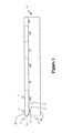
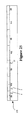
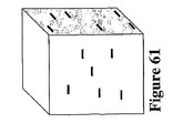
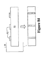
これらの三次元集積回路の特定の形成の議論の前に、出願人の出願中である米国特許出願番号09/950,909、 2001年9月12日出願 名称「薄膜およびその製造方法」にて説明されたように、起動基板の議論が提示される。選択的に接合された多層基板と称されたこの基板は、周知のようにウェーハ上のマルチプル・チップの処理を可能にするが、好ましくは機械的な研磨または他のエッチバック技術なしでのウェーハのチップ層の早急な除去を可能する。このチップ層は、後述するように、それから他のチップ層にスタックされることができる、あるいは、チップ層は、個々のチップにダイシング、および、スタックされることができる。 Prior to the discussion of the specific formation of these three-dimensional integrated circuits, the applicant's pending US patent application Ser. As explained, a discussion of the activation board is presented. This substrate, referred to as a selectively bonded multilayer substrate, allows processing of multiple chips on the wafer, as is well known, but preferably without mechanical polishing or other etch-back techniques The chip layer can be removed quickly. This chip layer can then be stacked on other chip layers, as described below, or the chip layer can be diced and stacked on individual chips.
図1を参照する。選択的に接合された多層基板100が示される。多層基板100は、露出された表面1Bを有する層1、および、選択的に層2の表面2Aに接着された層1Aを含む。層2は、対向する表面2Bをさらに含む。一般に、選択的に接合された多層基板100を形成するため、層1、層2または両方の層1および2は、弱い結合5および強い結合6の領域を定義するために処理されて、続いて接合される。ここにおいて、弱い結合5の領域は、有用な素子または構造の処理を可能にする状態にある。
概して、層1および2は互換性を持つ。すなわち、層1および2は、互換的、熱的、機械的、および/または結晶質の特性を構成する。特定の好ましい実施例において、層1および2は同じ材料である。もちろん、異なる材料は使用されることができるが、互換性のために好ましくは選ばれることができる。
Please refer to FIG. A selectively bonded
In general, layers 1 and 2 are interchangeable. That is, layers 1 and 2 constitute interchangeable, thermal, mechanical, and / or crystalline properties. In certain preferred embodiments,
層1の1つまたはそれ以上の領域は、1つまたはそれ以上の構造内またはその上で、マイクロエレクトロニクスは形成されることができるように基板領域として役立つように定義される。本願明細書においてさらに記載されるように、これらの領域は、いかなる所望のパターンであることができる。層1の選択された領域は、それから結合を最小化するために処理され、弱い結合領域5を形成する。代替的に、(層1の処理と連動して、または層1に対する処理の代わりに)層2の対応する領域は、結合を最小化するために処理されることができる。さらなる選択肢は、強い結合領域6の結合強さを強化するため、構造を形成するのに選ばれたそれら以外の領域における処理された層1および/または層2を含む。
層1および/または層2の処理後、層は、整列配置され、かつ、結合されることができる。さらに本願明細書において記載されるように、結合はいかなる適切な方法であってもよい。さらに、層の整列は、機械的、光学的またはその組合せであってよい。現段階では、やはり、概して層1の上に形成される構造がないので、整列は重大ではないと理解される。しかしながら、層1および2の両方が処理される場合、整列は選択された基板領域からの変化を最小化するために必要とされる可能性がある。
One or more regions of
After processing of
多層基板100は、層1の中にまたは上の所望の構造を処理するユーザに提供されることができる。したがって、多層基板100は、ユーザが従来の製造技術、または、様々な関連した技術が発展して公知となった他の技術を用いて構造または素子を処理することができるように形成される。特定の製造技術により基板は、高温度、圧力、苛酷な化学製品またはその組合せのような極端な状況にさらされる。したがって、多層基板100はこれらの状況に耐えるために好ましくは形成される。
有用な構造または素子は、部分的にまたは実質的に弱い結合領域5に重なる領域3の中または上で形成されることができる。したがって、部分的にまたは実質的に強い結合領域6に重なる領域4は、その中またはその上に構造を概して有しない。ユーザが多層基板100の層1の中または上に有用な素子を形成した後、層1は後に剥離されることができる。剥離は、有用な素子に不利益な層間剥離技術を直接受けさせる必要なく剥脱のような周知の技術により行われることができる。有用な素子は概して領域4の中または上に形成されないので、これらの領域は、領域3の中または上に形成される構造を損なわずにイオン注入のような剥離処理を受けさせられることができる。
Useful structures or elements can be formed in or on the
弱い結合領域5を形成するため、表面1A、2A、または両方は、弱い結合領域5の現場で実質的に非結合または弱い結合を形成するために処理されることができる。あるいは、弱い結合領域5は処理されないままにできる。それによって、強い結合領域6は強い結合を誘発するために処理される。領域4は、部分的にまたは実質的に強い結合領域6に重なる。強い領域4を形成するため、表面1A、2A、または両方は、強い結合領域6の現場で処理されることができる。あるいは、強い結合領域6は処理されないままにできる。それによって、弱い結合領域5は弱い結合を誘発するために処理される。さらに、両方の領域5および6は、異なる処理技術により処理されることができる。そこにおいて、処理は質的にまたは量的に異なる可能性がある。
In order to form the weak
弱い結合領域5および強い結合領域6の群の一方または両方の処理後、層1および2は、本質的に一体的な多層基板100を形成するために共に接合される。したがって形成されたように、例えば、特に層1の領域3の中または上に、構造または素子の中またはその上に形成するため、多層基板100はエンドユーザによって苛酷な環境を受けさせられる。
本明細書のため、「弱い結び付き」または「弱い結合」という語句は、例えば剥脱、他の機械的な分離、前述の剥離技術のうちの少なくとも1つからなる熱、光、圧力またはその組合せのような剥離技術によって直ちに克服されることができる層の層または部分の間の結合を概して称する。これらの剥離技術は、特に弱い結合領域5の近くで層1および2を最小限に離脱する、または、損なう。
After treatment of one or both of the group of
For the purposes of this specification, the phrase “weak bond” or “weak bond” refers to heat, light, pressure, or combinations thereof comprising, for example, exfoliation, other mechanical separation, at least one of the foregoing exfoliation techniques. Generally referred to as a bond between layers or portions of a layer that can be readily overcome by such peeling techniques. These stripping techniques detach from
弱い結合領域5および強い結合領域6の群の一方または両方の処理は、様々な方法によって達成されることができる。処理の重要な態様は、その弱い結合領域5が、(さらに本願明細書において記載される次の剥離ステップにおいて)強い結合領域6においてよりもより直ちに剥離されるということである。これが、剥離する間、その上に有用な構造を含むことができる領域3へのダメージを最小化する、または、防ぐ。さらに、強い結合領域6の介在物は、特に構造処理の間、多層基板100の機械的な保全性を強化する。したがって、その中またはその上の有用な構造によって除去される場合、層1の続いて起こる処理は最小化される、または、削除される。
The treatment of one or both of the group of weak
弱い結合領域に対する強い結合領域の結合強さの比率(SB/WB)は、一般に1より大きい。強い結合領域と弱い結合領域との特定の構成、および、強い結合領域と弱い結合領域との相対的な領域サイズ次第では、SB/WBの数値は、無限に接近することができる。すなわち、強い結合領域が処理の間、機械的および熱的な安定性を維持するためにサイズおよび濃度において十分な場合、弱い結合領域の結合強さは、ゼロに近づくことができる。 The bond strength ratio (SB / WB) of the strong bond region to the weak bond region is generally greater than one. Depending on the specific configuration of the strong and weak binding regions and the relative region sizes of the strong and weak binding regions, the SB / WB values can approach infinitely. That is, if the strong bond area is sufficient in size and concentration to maintain mechanical and thermal stability during processing, the bond strength of the weak bond area can approach zero.
しかしながら、従来技術において教示されているように、強い結合強さは、(SiO2ウェーハのような典型的シリコンおよびシリコン派生物において)約500ミリジュール/平方メートル(mj/m2)から、5000mj/m2以上まで変化することができるので、比率SB/WBは、相当に変化することができる。(本願明細書に参照された、Q. Y. Tong、U. Goesle 半導体ウェーハ結合、『科学および技術』pp. 104−118、John Wiley and Sons社、ニューヨーク、NY1999を参照のこと)
しかし、材料、意図された有用な構造(公知の場合)、選択された結合および剥離技術、弱い結合の領域と比較した強い結合の領域、ウェーハ上の強い結合および弱い結合構成またはパターンのなど次第で、弱い結合強さは、よりさらに相当変化することができる。例えば、イオン注入が層を剥離するステップとして使われるところで、有用な弱い結合領域の結合強さは、イオン注入および/または注入された領域での微小気泡の関連した放出の後強い結合領域の結合強さと同等であることができる。したがって、選択された剥離技術、および、弱い結合領域において形成されるおそらく有用な構造または素子の選択次第で、結合強さSB/WBの比率は、概して1より大きく、好ましくは2、5、10を超えるかまたはより高い。
However, as taught in the prior art, strong bond strengths range from about 500 millijoules / square meter (mj / m 2 ) to 5000 mj / (in typical silicon and silicon derivatives such as SiO 2 wafers). Since it can vary up to m 2 or more, the ratio SB / WB can vary considerably. (See QY Tong, U. Goesle Semiconductor Wafer Bonding, Science and Technology, pp. 104-118, John Wiley and Sons, New York, NY 1999, referenced herein)
However, depending on the material, intended useful structure (if known), selected bonding and debonding techniques, areas of strong bonding compared to areas of weak bonding, strong bonding on wafer and weak bonding configurations or patterns, etc. Thus, the weak bond strength can vary considerably further. For example, where ion implantation is used as a delamination step, a useful weak bond region bond strength is the strong bond region bond after ion implantation and / or associated release of microbubbles in the implanted region. Can be equivalent to strength. Thus, depending on the chosen stripping technique and the choice of a possibly useful structure or element formed in the weakly bonded region, the ratio of bond strength SB / WB is generally greater than 1, preferably 2, 5, 10 Or higher.
弱い結合領域5および強い結合領域6の群の一方または両方の処理の特定のタイプは、概して選ばれる材料次第で始められる。さらに、層1および2の結合技術の選択は、少なくとも一部分で、選択された処理手順次第である可能性がある。加えて、続いて起こる剥離は、処理技術、結合方法、材料、有用な構造の存在のタイプ、前述の要因のうちの少なくとも1つからなる組合せのような要因次第である可能性がある。特定の実施例において、処理、結合および続いて起こる剥離(すなわち領域3、または、代替的により高水準装置における中間の構成要素における有用な構造を形成するエンドユーザにより行われる)の選択された組合せは、層2から層1を剥離するために劈開伝播、または層2を除去する機械的な薄層化の必要性を除去し、好ましくは、劈開伝播および機械的な薄層化の両方を除去する。したがって、従来の教示に従う劈開伝播または機械的な薄層化は層2ダメージを与え、さらに大幅な処理なしでは本質的に役立たなくさせるので、下側基板は、最小のまたは未処理で再利用されることができる。
The particular type of treatment of one or both of the group of
図2および3を参照する。ここにおいて、同様に状態にある領域は、参照の数字のように参照される。ある処理技術は、表面1A、2Aまたは1Aおよび2Aの両方の上に固体の構成要素および分解できる構成要素を含むスラリーの使用を含む。固体の構成要素は、例えば、アルミナ、酸化シリコン(SiO(x))、他の固体の金属または金属酸化物、または層1および2の結合を最小化する他の材料である可能性がある。分解できる構成要素は、例えば、ポリビニルアルコール(PVA)または適切な分解できる他のポリマーである可能性がある。概して、スラリー8は表面1A(図2)、2A(図3)または両方の1Aおよび2Aで弱い結合領域5において適用される。続いて、層1および/または2は、ポリマーを分解するため、好ましくは不活発な環境で加熱されることができる。したがって、多孔性構造(スラリーの固体の構成要素からなる)は弱い結合領域5で残り、結合の時点で層1および2は弱い結合領域5で結合をしない。
Reference is made to FIGS. Here, regions in the same state are referred to as reference numerals. One processing technique involves the use of a slurry that includes solid components and degradable components on
図4および5を参照すると、他の処理技術は、弱い結合領域5と強い結合領域6との間の表面粗さにおける変化に依存する可能性がある。表面粗さは、表面1A(図4)、表面2A(図5)または、表面1Aおよび2Aの両方で変更されることができる。一般に、弱い結合領域5は、強い結合領域6より高い表面粗さ7(図4および5)を有する。半導体材料において、例えば、弱い結合領域5は、約0.5ナノメートル(nm)を超える表面粗さを有することができ、強い結合領域4は、概して約0.5nm未満のより低い表面粗さを有することができる。
With reference to FIGS. 4 and 5, other processing techniques may rely on changes in surface roughness between weak and
他の例では、弱い結合領域5は約1nmを超える表面粗さを有することができ、強い結合領域4は概して約1nm未満のより低い表面粗さを有することができる。さらなる例において、弱い結合領域5は約5nmを超える表面粗さを有することができ、強い結合領域4は概して約5nm未満より低い表面粗さを有することができる。表面粗さは、エッチング(例えば、KOHまたはHF溶液において)、または、沈着プロセス(例えば、低圧化学蒸着法「LPCVD」またはプラズマ拡張化学蒸着法「PECVD」)によって変更されることができる。表面粗さと関連した結合強度は、本願明細書において参照された、例えば、Guiその他による「表面粗さ制御による選択的なウェーハ結合」電気化学会ジャーナル 148(4)G225−G228(2001)において、より完全に記載される。
In other examples, the
これと同様の方法で(ここにおいて、同様な状態にある領域は、図4および5に記載の類似した参照番号によって参照される)多孔性領域7は、弱い結合領域5で形成されることができ、強い結合領域6は処理されていないままである可能性がある。したがって、層1はその多孔性の性質のために弱い結合領域5の現場で、層2と最小限に結合する。有孔率は、表面1A(図4)、表面2A(図5)または1Aおよび2Aの両方の表面において変更されることができる。一般に、弱い結合領域5は、多孔性領域7(図4および5)において、強い結合領域6よりも高い有孔率を有する。
In a similar manner (where the region in a similar state is referred to by a similar reference number described in FIGS. 4 and 5), the porous region 7 can be formed with a weak
他の処理技術は、エッチングされた領域においてフォトレジストまたは炭素を含む他の材料の沈着(例えば、重合体ベースの分解できる材料を含む)に続いて(表面1A(図4)、2A(図5)または1Aおよび2Aの両方ともにおいて)弱い結合領域5の選択的なエッチングに依存する可能性がある。キャリア部材を分解するために十分な温度で好ましくは、層1および2が結合すると、弱い結合領域5は、多孔性炭素材料をその中に含む。したがって、弱い結合領域5の層1と2と間の結合は、強い結合領域6における層1と2との間の結合と比較して、非常に弱い。当業者は、状況次第で、分解材料は、除気しない、汚染しない、または、他の点で基板層1または2、または領域3の中または上に形成される有用な構造を汚染しないものが選ばれることを認識するであろう。
Other processing techniques follow (
さらなる処理技術は、強い結合領域6および/または弱い結合領域5を達成するため照射を使用することができる。この技術においては、層1および/または2は、必要に応じて、強いおよび/または弱い結合を達成するために中性子、イオン、粒子線またはその組合せによって照射を受ける。例えば、He+、H+のような粒子、または、他の適切なイオンまたは粒子、電磁エネルギ、または、レーザー光線は、(表面1A(図10)、2A(図11)または1Aおよび2Aの両方ともにおける)強い結合領域6で照射を受けることができる。照射のこの方法は、照射量および/または注入エネルギが概して非常により少ない(例えば、剥離のために使用する適用量は順に百分の一から千分の一である)ということにおいて、層の剥離のためのイオン注入と異なると理解されるべきである。
Further processing techniques can use irradiation to achieve a strong
図8および9を参照する。なおさらなる処理技術は、弱い結合領域5の表面エッチングを含む。このエッチング・ステップの間、柱9は、表面1A(図8)、2A(図9)または1Aおよび2Aの両方ともの上の弱い結合領域5において定義される。柱は、柱を残した選択エッチングによって定義されることができる。柱の形状は、三角形、ピラミッド型、矩形、半球状、または他の適切な形状である可能性がある。
Reference is made to FIGS. Still further processing techniques include surface etching of the
あるいは、柱は伸ばされる、またはエッチングされた領域に置かれることができる。結合材料のための結合位置が少ないので、弱い結合領域5の全体の結合強さは、強い結合領域6の結合強さよりも非常に弱い。
Alternatively, the pillar can be stretched or placed in an etched area. Since there are few bond positions for the bond material, the overall bond strength of the
さらにもう1つの処理技術は、層1(図12)、2(図13)において弱い結合領域5に、例えばエッチング、機械加工または両方(使用される材料に次第で)によって形成されたボイド領域10(図12および13)の介在物を含む。したがって、第1の層1が第2の層2に接合する場合、続いて起こる剥離を容易にする強い結合領域6と比較すると、ボイド領域10は結合を最小化する。
Yet another processing technique is the
再び図2および3を参照すると、他の処理技術は、表面1A(図2)、2A(図3)または1Aおよび2Aの両方の弱い結合領域5で、1つまたはそれ以上の金属領域8の使用を含む。例えば、Cu、Au、Pt、または、その組合せまたは合金を含むがそれらに限定されない金属は、弱い結合領域5に置かれる。層1および2が結合すると、弱い結合領域5は、弱く結合される。強い結合領域は、処理されていないままであり、(ここにおいて、結合強さの差は、弱い結合層5および強い結合領域6に関して弱い結合比に対する必要な強い結合を提供する)または、強い凝着を促進するため、上記に記載された、または下記のように処理されることができる。
Referring again to FIGS. 2 and 3, other processing techniques include
さらなる処理技術は、表面1A(図10)、2A(図11)または1Aおよび2Aの両方の上の強い結合領域6で、1つまたはそれ以上の凝着促進剤11の使用を含む。
適切な凝着促進剤は、TiO(x)、タンタル酸化物または他の凝着促進剤を含むが、これに限定されるものではない。代わりとして、凝着促進剤は表面1Aおよび/または2Aの実質的にすべてに使われることができ、ここにおいて、金属材料は、凝着促進剤と表面1Aまたは2A(凝着促進剤の現場に次第で)との間で、弱い結合領域5において配置される。結合すると、したがって金属材料は、弱い結合領域5での強い結合を妨げ、一方で、強い結合領域6で残っている凝着促進剤は、強い結合を促進する。
Further processing techniques include the use of one or
Suitable adhesion promoters include, but are not limited to, TiO (x), tantalum oxide or other adhesion promoters. Alternatively, the adhesion promoter can be used on substantially all of the
さらにもう1つの処理技術は、疎水性および/または親水性(訳注*5)の異なる領域の提供を含む。例えば、シリコンのような材料は自然に室温で結合するので、親水性領域は特に強い結合領域6のために有用である。
Yet another processing technique involves providing different regions of hydrophobic and / or hydrophilic properties. For example, a hydrophilic region is useful for a particularly
室温でおよび上昇された温度の両方における疎水性のおよび親水性の結合技術は、例えば、本願明細書において参照された、Q. Y. Tong、U. Goesle 半導体ウェーハ結合、『科学および技術』pp. 49−135、John Wiley and Sons社、ニューヨーク、NY1999 に記載されているように、公知である。
Hydrophobic and hydrophilic bonding techniques at both room temperature and elevated temperature are described, for example, in QY Tong, U. Goesle Semiconductor Wafer Bonding, Science and Technology, pp. 49- 135, John Wiley and Sons, New York, NY 1999.
なおさらなる処理技術は、選択的に照射を受ける1つまたはそれ以上の剥脱層を含む。例えば、1つまたはそれ以上の剥脱層は、表面1Aおよび/または2Aに配置されることができる。照射なしでは、剥脱層は接着材として作用する。
Still further processing techniques include one or more exfoliation layers that are selectively irradiated. For example, one or more exfoliation layers can be disposed on
弱い結合領域5における紫外照射のような照射に露出されると、接着特性は最小化される。有用な構造は、弱い結合領域5の中または上で形成されることができ、次の紫外照射ステップまたは他の剥離技術は、強い結合領域6で、層1および2を分離するために用いることができる。
When exposed to radiation such as ultraviolet radiation in the
図6および7を参照する。追加的な処理技術は、熱的に処理されると、弱い領域3の層1(図6)、層2(図7)または層1および層2の両方で複数の微小気泡13の形成を可能にするため、注入イオン12(図6および7)を含む。したがって、層1および2が接合する場合、弱い結合領域5の層1および2の次の剥離が容易にされるように、強い結合領域6以外の弱い結合領域5は結合する。
Reference is made to FIGS. Additional processing techniques allow the formation of
他の処理技術は、エッチング・ステップに続くイオン注入ステップを含む。一実施例において、この技術は、表面1Bの実質的にすべてを通じてイオン注入が実行される。続いて、弱い結合領域5は、選択的にエッチングされることができる。この方法は、本願明細書において参照されたシンプソンその他の、「燐化インジウムの選択的な化学エッチングの誘発された注入」電気化学および固体物理会報4(3)G26−G27 において、欠陥を除去するためのダメージ選択エッチングに関して記載される。
Other processing techniques include an ion implantation step following the etching step. In one embodiment, this technique performs ion implantation through substantially all of surface 1B. Subsequently, the
なおさらなる処理技術においては、弱い結合領域5および/または強い結合領域6に選択的に置かれる1つまたはそれ以上の層が、狭いまたは広い波長範囲に基づく放射線を吸収および/または反射する特性を有するということが認識される。例えば、強い結合領域6に選択的に置かれる1つまたはそれ以上の層は、特定の放射線波長に露出されると、層が強い結合領域6で放射線を吸収し、層1および2を結合するように接着特性を有することができる。
In still further processing techniques, one or more layers selectively placed in the
当業者は、前述の処理技術のうちの少なくとも1つからなる組合せと同様に、追加的な処理技術が使用されることができると認識するであろう。しかしながら、使用されるいかなる処理の主な特長は、1より大きいSB/WB結合強さ比率を提供する弱い結合の1つまたはそれ以上の領域および強い結合の1つまたはそれ以上の領域を形成する能力である。
層1および2の界面における弱い結合領域5および強い結合領域6の形状は、領域3においてまたはその中に形成される有用な構造のタイプ、選択された剥離/結合のタイプ、選択された処理技術、および他の要因を含むがこれに限らない要因に従って変化する可能性がある。
Those skilled in the art will recognize that additional processing techniques can be used, as well as combinations of at least one of the foregoing processing techniques. However, the main feature of any treatment used is the formation of one or more regions of weak bonds and one or more regions of strong bonds that provide an SB / WB bond strength ratio greater than one. It is ability.
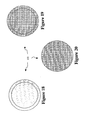
The shape of the
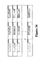
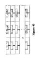
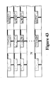
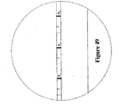
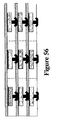
図14−20を参照する。多層基板100は、同心円(図14、16、および18)、縞模様(図15)、放射状(図17)、格子縞模様(図20)、格子縞および環状の組合せ(図19)、または、そのいかなる組合せによって弱い結合および強い結合領域を有することができる。もちろん、当業者は、いかなる形状も選ばれることができることを認識するであろう。さらに、強い結合の領域と比較した弱い結合の領域の比率は、変化することができる。一般に比率は、特に構造処理の間、多層構造100の完全性を包含しないように(すなわち強い結合領域6で)十分な結合を提供する。
Reference is made to FIGS. The
好ましくは、比率は、また構造処理のための有用な領域(すなわち弱い結合領域5)を最大にする。 Preferably, the ratio also maximizes the useful area for structural processing (i.e. weak binding area 5).
上述のように弱い結合領域5および/または強い結合領域6の実質的に現場において表面1Aおよび2Aの一方または両方の処理後、層1および2は、実質的に一体的な多層基板100を形成するために共に接合する。層1および2は、共晶、融解、陽極、真空、ファン・デル・ワールス、化学的な凝着、疎水性現象、親水性現象、水素結合、クーロン力、毛管の力、非常に短い範囲の力、または前述の結合技術および/または物理的な現象のうちの少なくとも1つからなる組合せを含むがこれに限らない、様々な技術および/または物理的な現象の1つにより、共に接合する。もちろん、結合技術および/または物理的な現象は、ある程度使用される1つまたはそれ以上の処理技術、その上にまたはその中に形成される有用な構造のタイプまたは存在、予期された剥離方法、または、他の要因次第であることは当業者にとって明らかである。
After treatment of one or both of the
代替的に、埋込み酸化物層は、素子層の底面で形成されることができる。酸化物層は、バルク性基板への素子層の選択的な結合の前に形成されることができる。さらに、酸化物層は、所望の埋込み酸化物層の深さに酸素を注入して形成されることができる。
酸化物層を多層基板の上に形成するための様々な技術がある。
Alternatively, the buried oxide layer can be formed on the bottom surface of the device layer. The oxide layer can be formed prior to selective bonding of the device layer to the bulk substrate. Further, the oxide layer can be formed by implanting oxygen to the desired buried oxide layer depth.
There are various techniques for forming an oxide layer on a multilayer substrate.
第1の技術は、1300℃より高温でのアニールに続く高照射量での酸素の注入によるシリコン基板の埋込みSiO2層の形成から構成される。イオン注入を通じて、埋込みSiO2層の所望の層厚が形成されることができる。 The first technique consists of forming a buried SiO 2 layer in a silicon substrate by oxygen implantation at a high dose following an anneal at a temperature higher than 1300 ° C. Through ion implantation, the desired layer thickness of the buried SiO 2 layer can be formed.
埋込み酸化物層を構成するための代替技術は、細いSiO2フィルムの多層基板の表面の上への形成、そしてSiO2フィルムによる第2のシリコン基板への基板の結合から構成される。周知の機械的な研磨および研磨加工プロセスは、それから埋込みシリコン酸化層より上に所望の層厚シリコン層を形成するために用いられる。多層基板上のシリコン酸化層は、所望の層厚を得るために形成された酸化物層のエッチングに続いて、表面の連続した酸化によって形成される。 An alternative technique for constructing the buried oxide layer consists of forming a thin SiO 2 film on the surface of the multilayer substrate and bonding the substrate to a second silicon substrate with the SiO 2 film. Well known mechanical polishing and polishing processes are then used to form the desired layer thickness silicon layer above the buried silicon oxide layer. A silicon oxide layer on the multilayer substrate is formed by continuous oxidation of the surface following etching of the oxide layer formed to obtain the desired layer thickness.
埋込み酸化物層を形成するための他の技術は、酸化による第1の多層基板上の細いシリコン酸化層の形成、それから、細いシリコン酸化層の下で空胴平面を形成するため、H+イオンの第1の多層基板の中への注入から構成される。 Another technique for forming the buried oxide layer is to form a thin silicon oxide layer on the first multi-layer substrate by oxidation, and then to form a cavity plane under the thin silicon oxide layer. Of the first multi-layer substrate.
続いて、細いシリコン酸化層によって、この第1の本体は第2の多層基板に接合し、そうすると、全体のアセンブリは割れている平面に空胴平面を変換するために熱的な活性化を受けさせられる。これは、使用可能なSOI基板の回復を可能にさせる。 Subsequently, a thin silicon oxide layer joins this first body to the second multilayer substrate, so that the entire assembly undergoes thermal activation to convert the cavity plane into a cracked plane. Be made. This allows recovery of the usable SOI substrate.
多層基板100は、したがってエンドユーザ(埋込み酸化物層の有無にかかわらず)に提供されることができる。あるいは、導線の特定のパターンは、多層基板と一体的に形成されることができる。エンドユーザは、実質的にまたは部分的に、表面1Aおよび2Aの界面で弱い結合領域5に重なる領域3の中または上で1つまたはそれ以上の有用な構造(図示せず)続いて形成することができる。有用な構造は、1つまたはそれ以上の能動または受動的な要素、素子、道具、ツール、チャネル、他の有用な構造、または、前述の有用な構造のうちの少なくとも1つからなるいかなる組合せを含むことができる。例えば、有用な構造は集積回路または太陽電池を含むことができる。もちろん、当業者は様々なマイクロ技術および微小工学ベースの素子が形成されることを認識する。
The
例えば、能動素子は多層SOIウェーハまたは基板の上に形成されることができる。これらの能動素子は、SOI基板の埋込み酸化膜上の単結晶シリコン活動層において形成される。シリコン活動層の層厚は、その中に形成される能動素子の目的に依存する。SOI要素が高速および低消費電力で作動しているCMOS要素である場合、能動層の層厚は、約50から100nmである。SOI要素が高降伏電圧要素である場合、能動層の層厚は、数マイクロメートルである。能動素子の例は、保護用ダイオードである。保護用ダイオードは、コネクション・ピンからの過電流を基板および半導体デバイスの外側まで導き、このことにより半導体デバイスの内部回路を保護するため、半導体デバイスに提供される半導体要素である。 For example, the active device can be formed on a multilayer SOI wafer or substrate. These active elements are formed in the single crystal silicon active layer on the buried oxide film of the SOI substrate. The layer thickness of the silicon active layer depends on the purpose of the active device formed therein. If the SOI element is a CMOS element operating at high speed and low power consumption, the layer thickness of the active layer is about 50 to 100 nm. When the SOI element is a high breakdown voltage element, the layer thickness of the active layer is a few micrometers. An example of an active element is a protective diode. A protective diode is a semiconductor element provided to a semiconductor device to conduct overcurrent from the connection pins to the outside of the substrate and the semiconductor device, thereby protecting the internal circuitry of the semiconductor device.
他の能動素子が、単結晶シリコン基板またはSOI基板のどちらかの動作領域の選択的なドープおよびマスキングによって製造されることができることは、当業者にとって明らかである。これらの能動素子は、バイポーラ接合トランジスタ、MOSトランジスタ、電界効果トランジスタ、ダイオード、絶縁ゲート・バイポーラトランジスタなどを含むが、これに限定されるものではない。 It will be apparent to those skilled in the art that other active devices can be fabricated by selective doping and masking of the operating region of either a single crystal silicon substrate or an SOI substrate. These active elements include, but are not limited to, bipolar junction transistors, MOS transistors, field effect transistors, diodes, insulated gate / bipolar transistors, and the like.
多層基板上に製造されることができる他の能動素子は、MEMS装置である。概して、MEMS装置は、基板上に製造された電極に対向して配置された電極および作動可能な要素からなる。作動可能な要素は、マシン構造上に電気的制御を提供するため、電極からの制御を搬送する。 Another active device that can be fabricated on a multilayer substrate is a MEMS device. In general, a MEMS device consists of an electrode and an actuatable element disposed opposite to an electrode manufactured on a substrate. The actuatable element carries control from the electrodes to provide electrical control over the machine structure.
MEMS装置を製造する1つの技術は、それがMEMS構造を形成するため、単一の基板層から材料をエッチングして離すことを含むので減ずる製造技術と考えられる深いエッチング処理を用いた基板のバルク性ミクロ機械加工である。 One technique for manufacturing a MEMS device is to bulk a substrate using a deep etching process that is considered a manufacturing technique that reduces as it forms a MEMS structure and involves etching away material from a single substrate layer. Micromachining.
基板層は、およそ何十ミクロンで比較的厚く、このプロセスの高度の知識により、カンチレバー、ブリッジ、溝、空胴、ノズルおよび膜のような、基板上の異なる構造のミクロ機械加工を可能にする。 The substrate layer is relatively thick on the order of tens of microns, and advanced knowledge of this process allows micromachining of different structures on the substrate, such as cantilevers, bridges, grooves, cavities, nozzles and membranes. .
多層基板上にMEMS装置を製造する他の技術は、表面ミクロ機械加工技術による。代替的な構造上の層および犠牲のスペーサ層が、必要な機械的なおよび電気特性でMEMS構造を造るために“組み立てられ”ているので、それは添加処理と考えられる。多結晶シリコン(ポリシリコン)は最も一般に使われる構造材料であり、酸化シリコン・ガラスは最も一般的には使用される犠牲材料である。従来のミクロ機械加工プロセスにおいて、これらの層は、窒化ケイ素の層によって絶縁されるシリコン基板上のポリシリコン/酸化物の対において形成される。層は、モーター、ギア、鏡およびビームのような複雑な構造を形成するため、フォトリトグラフィ技術を使用してパターン化される。層が造られると、切削は、酸化物層で作成され、上部構造上の層を基板にまたは下にある構造上の層に固定するためにポリシリコンで満たされる。 Another technique for manufacturing MEMS devices on multilayer substrates is by surface micromachining techniques. Since alternative structural layers and sacrificial spacer layers are “assembled” to build a MEMS structure with the necessary mechanical and electrical properties, it is considered an additive process. Polycrystalline silicon (polysilicon) is the most commonly used structural material, and silicon oxide glass is the most commonly used sacrificial material. In conventional micromachining processes, these layers are formed in polysilicon / oxide pairs on a silicon substrate that is insulated by a layer of silicon nitride. The layers are patterned using photolithography techniques to form complex structures such as motors, gears, mirrors and beams. Once the layer is built, the cut is made with an oxide layer and filled with polysilicon to secure the top structural layer to the substrate or to the underlying structural layer.
1つまたはそれ以上構造が、層1の1つまたはそれ以上の選択された領域3の上に形成された後、層1は様々な方法により剥離されることができる。いうまでもなく、構造が部分的にまたは実質的に弱い結合領域5に重なる領域4の中または上で形成されるので、層1の剥離は、構造上の欠陥または変形のような、剥離に関連する構造への典型的損害を最小化または除去する一方で、生じることができる。
剥離は、様々な周知の技術によって達成されることができる。一般に剥離は、少なくとも一部において、処理技術、結合技術、材料、有用な構造のタイプまたは存在、または他の要因の存在次第である可能性がある。
After one or more structures have been formed on one or more selected
Stripping can be accomplished by various well-known techniques. In general, delamination can depend, at least in part, on the presence of processing techniques, bonding techniques, materials, useful structure types or presence, or other factors.
一般に図21−32を参照すると、剥離技術は、概して層1の層厚と同等の基準深で微小気泡を形成するためにイオンまたは粒子の注入に基づくことができる。イオンまたは粒子は、酸素、水素、ヘリウムまたは他の粒子14から生じられる。注入(訳注*6)は、粒子またはイオンに微小気泡15を生じさせるため、強い電磁放射、熱、光(例えば赤外線または紫外線)、圧力、または前述のうちの少なくとも1つからなる組合せへの露出によって続き、層1および2を最終的に展開および剥離させる。注入および任意に熱、光、および/または圧力はまた、例えば、層1および2の平面に並列である層1および2の平面に垂直の方向、層1および2の平面の他の角度の剥脱方向(図23、26、29、32で破線により示された)またはその組合せにおいて機械的な分離ステップ(図23、26、29、32)によって続くことができる。薄膜層の分離のためのイオン注入は、本願明細書において参照されたチャンその他による米国特許No.6,027,988 名称「プラズマ浸入イオン注入によりフィルムをバルク性基板から分離する方法」においてさらに詳細に記載される。
Referring generally to FIGS. 21-32, the stripping technique can be based on ion or particle implantation to form microbubbles at a reference depth generally equivalent to the layer thickness of
特に図21−23および24−26を参照すると、層1および2の間の界面は、特に強い結合領域6で微小気泡17を特に形成するため、選択的に注入されることができる。このように、領域3(その中またはその上に1つまたはそれ以上の有用な構造を有する)の粒子16の注入は、最小化され、したがって、領域3において1つまたはそれ以上の有用な構造に発生する修理可能または回復不能なダメージの可能性を減少することができる。選択的な注入は、強い結合領域4(図24−26)の選択的なイオンビーム走査または領域3(図21−23)のマスキングによって実行されることができる。選択的なイオンビーム走査は、構造100の機械的な操作および/または注入されるイオンまたは粒子を誘導するのに用いられる素子を指す。当業者に公知であるように、様々な装置および技術は、集中するイオンビームおよび電磁ビームを含むがそれに限られない選択的な走査を実行するために使用されることができる。さらに、様々なマスキング材料および技術もまた公知である。
With particular reference to FIGS. 21-23 and 24-26, the interface between
図27−29を参照すると、注入は、表面1Bまたは2B全体を実質的に横切って達成されることができる。注入は、ターゲット、注入材料および注入の所望の深さに従う適切なレベルにある。したがって、層2が層1より非常に厚い所で、表面2Bを通じて注入するのは実際的でないかもしれないが;層2が適切な注入層厚である場合、(例えば、実行可能な注入エネルギの範囲内で)、表面2Bを通じて注入することは、望ましい可能性がある。これは、領域3の1つまたはそれ以上の有用な構造に発生する可能性がある修理可能または回復不能なダメージの可能性を最小化するかまたは除去する。
一実施例において、図18と関連して図30−32を参照すると、強い結合領域6は、層1と2との間の界面の外周で形成される。
Referring to FIGS. 27-29, implantation can be accomplished substantially across the entire surface 1B or 2B. The implant is at an appropriate level according to the target, the implant material and the desired depth of implantation. Thus, it may not be practical to implant through surface 2B where
In one embodiment, referring to FIGS. 30-32 in conjunction with FIG. 18, a
したがって、層1を層2から剥離するため、イオン18は、例えば、層1および1の界面で微小気泡を形成するために領域4を通じて注入されることができる。好ましくは、選択的な走査が使用される。ここにおいて、構造100(矢印20で示された)は、回転することができ、走査装置21(矢印22で示された)、またはその組合せは、回転することができる。本実施例におけるさらなる利点は、その中またはその上に形成される有用な構造の選択をエンドユーザに与える可撓性である。強い結合領域6の寸法(すなわち幅)は、多層基板100の機械的および熱的な保全性を維持するために適切である。好ましくは、強い結合領域6の寸法は最小化され、したがって構造処理のための弱い結合領域5の領域を最大にする。例えば、強い結合領域6は、8インチのウェーハ上での1ミクロンである。
さらに、層1の層2からの剥離は、例えば強い結合領域6でエッチングを作成するための(表面に並行した)エッチングのように他の従来の方法によって始められることができる。このような実施例では処理技術は、特に互換性を持ち、例えばここにおいて、強い結合領域6は、その集合体(すなわち層1および2)の選択性よりも非常により高いエッチング選択性を有する酸化物層で処理される。弱い結合領域5は、選択された処理またはその欠如が層1と層2との接合ステップにおいて接合が妨げるので、弱い結合領域5の現場で層2から層1を剥離するために好ましくはエッチングを必要としない。
これに対して、劈開伝播は、層1の層2からの剥離を始めるために用いることができる。また、弱い結合領域5の結合は限られるので、剥離は好ましくは強い結合領域6の現場で必要とされるのみである。さらに、剥離は、従来公知であるように、エッチング(表面に垂直の)によって始められ、好ましくは、領域4の現場(すなわち、部分的にまたは実質的に、強い結合領域6が重なる)に限られる。
Thus, to separate
Furthermore, peeling of
In contrast, cleavage propagation can be used to initiate delamination of
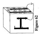
他の実施例において、次に図85を参照して、剥離する方法が示される。方法は、多層基板100の提供;WB領域5における1つまたはそれ以上の有用な構造(図示せず)の処理;好ましくは先細角(例えば45°)で、SB領域6のエッチング;素子層への、好ましくはエッチングされたSB領域6だけへの低エネルギ・イオン注入;および、WB領域での素子層部の剥離、または速やかな除去;を含む。WB層の2つの素子層部は除去されると示される一方で、これが1つの素子層部上の解放を容易にするために用いることができると理解されることに留意する。WB領域の先細端は、機械的に削除を容易にする。有益に、元々の素子層厚を貫通するため、必要とされる注入エネルギと比較すると非常に低いイオン注入エネルギが使われることができる。
In another embodiment, referring now to FIG. 85, a method for stripping is shown. The method includes providing a
層1および2は、同じまたは異なる材料であることができ、プラスチック(例えばポリカーボネート)、金属、半導体、絶縁物、単結晶、アモルファス、非結晶、生物学的材料(例えば、DNAベースのフィルム)、または、前述の材料のタイプの少なくとも1つからなる組合せを含むがこれに限らない材料を含むことができる。例えば、材料の特定のタイプの材料は、シリコン(例えば、単結晶、多結晶、非結晶、ポリシリコン、および、Si3N4、SiC,SiO2のような派生物)、GaAs,InP、CdSe、CdTe、SiGe、GaAsP、GaN、SiC、GaAlAs、InAs、AlGaSb、InGaAs、ZnS、AlN、TiN、他のIIIA−VA材料群、IIB材料群、VISA材料群、サファイヤ、クォーツ(結晶またはガラス)、ダイヤモンド、シリカおよび/またはシリケートベースの材料、前述の材料の少なくとも1つからなる材料の組合せを含む。もちろん、他のタイプの材料の処理は、所望の組成物の多層基板100を提供するため、本願明細書において記載されるプロセスから利益を得ることができる。特に本願明細書において記載された方法のために適切である好適な材料は、層1として半導体材料(例えばシリコン)および層2として半導体材料(例えばシリコン)を含み、半導体(層1)またはガラス(層2);シリコンカーバイド(層2)上の半導体(層1)、サファイヤ(層2)上の半導体(層1);サファイヤ(層2)上のGaN(層1);ガラス(層2)上のGaN(層1);シリコンカーバイド(層2)上のGaN(層1);プラスチック(層2)上のプラスチック(層1)、ここにおいて、層1および2は、同じまたは異なるプラスチックである;および、ガラス(層2)上のプラスチック(層1)の組合せを含むが、これに限定されるものではない。
層1および2は、フィルムおよび/または基板構造を形成するため堆積するウェーハまたは流体材料を含む様々な供給源に由来することができる。ここで開始材料は、ウェーハの形であり、いかなる従来のプロセスも、層1および/または2を導くために用いることができる。例えば、層2はウェーハから構成されることができ、層1は同じまたは異なるウェーハの一部から構成されることができる。層1を構成しているウェーハの部分は、機械的な薄層化(例えば、機械的な研磨、切断、研磨加工;化学的な機械研磨;研磨停止;または前述の少なくとも1つを含む組合せ)、劈開伝播、機械的な分離(例えば、構造100の平面に垂直で、かつ、剥脱方向において構造100の平面に並列の劈開伝播、または、その組合せ)に続くイオン注入、層分割を誘発する熱、光および/または圧力によって続くイオン注入、化学エッチング等から導かれる。さらに、層1および2のどちらかまたは両方は、例えば化学蒸着法、エピタキシャル成長方法等により、堆積または伸張されることができる。
即時の方法および結果として発生する多層基板または多層基板に由来する薄膜の重要な利益は、構造は、部分的にまたは実質的に弱い結合領域5に重なる領域3の中または上に形成されることである。このことは、層1が層2から除去される場合、実質的に有用な構造へのダメージの可能性を最小化または除去する。剥離ステップは、一般に注入(例えばイオン注入)、力の適用、または、層1および2を剥離するために必要とされる他の技術を必要とする。
An important benefit of the immediate method and the resulting multilayer substrate or the thin film derived from the multilayer substrate is that the structure is formed in or on a
特定の実施例において、構造は、構造に回復可能または回復不能なダメージを与える可能性がある局所的注入、力の適用または他の処理ステップを必要としない領域3の中または上にあるので、層1は除去され、構造を修復する次の処理なしで、構造はそこから導かれることができる。強い結合領域6に部分的にまたは実質的に重なる領域4は、一般にその上に構造を有しない。したがって、これらの領域4は、構造へのダメージなく注入または力を受けることができる。
In certain embodiments, because the structure is in or on
層1は、自立したフィルムまたは支持されたフィルムとして除去されることができる。例えば、ハンドルは、層1が層2から除去されるように、層1への取付けのために一般に使用され、ハンドルによって支持されたままである。一般にハンドルは、続いてフィルム、または、その部分(例えば1つまたはそれ以上有用な構造を有する)、他の処理されたまたは代替的にハンドル上に残留するフィルムを意図された基板上に配置するために用いることができる。
即時の方法の1つの利益は、層2を構成している材料が再利用およびリサイクルされることができることである。単一ウェーハは、例えば、いかなる周知の方法によって層1を導くために使われることができる。導かれた層1は、上記に記載の残りの部分(層2)に選択的に接合されることができる。薄膜が剥離される場合、次の層1として使用される薄膜を得るため、層2の残りの部分を用いて、プロセスは反復される、層1のための薄膜を導くための層2の残りの部分の使用は、それがもはや実行可能または実用的でなくなるまで、反復されることができる。
One benefit of the immediate method is that the
上記のように、選択的に接合された多層基板の形成が詳述され、三次元集積回路の形成が、選択的に接合された多層基板を使用して次に記載される。 As described above, the formation of a selectively bonded multilayer substrate is described in detail, and the formation of a three-dimensional integrated circuit is next described using a selectively bonded multilayer substrate.
図80を参照する。スタック1...Nウェーハおよびそこからのダイカットの等大の概略図が、示される。明確にするため、座標および定義が示されている。ダイおよびウェーハのスタックは、本願明細書において一般に平面方向として指されるxおよびy座標方向において延長する上部および底面および中間の層を一般に有する。平面方向が表面または中間の層に延長しているいかなる方向も含むことに注意する。いくつかの層は、本願明細書において垂直または三次元と一般に指されるz方向においてスタックされる。
Reference is made to FIG.
ダイカットの後、中間の層および上部および底面に加えて、ダイはz方向において一般に延長している4つのエッジ面を有する。 After die cutting, in addition to the middle layer and the top and bottom surfaces, the die has four edge faces that generally extend in the z direction.
次に図33を参照すると、上述の通り、強い接合領域3および弱い接合領域4を有する選択的に接合された基板100が提供される。図示された実施例が図18で一般に強い結合パターンを有するにもかかわらず、強い結合領域3および弱い結合領域4のいかなるパターンも利用されると理解される。ここにおいて、上記に記載および言及されたように、回路網または他の有用な素子は、弱い結合領域で形成される。
Referring now to FIG. 33, a selectively bonded
特に本発明は、逐次処理ステップの数を減少させる一方で、機能強化と同様、様々な追加的な機能が提供されることができるという点で、上述したIBMの米国特許No.6,355,501において都合が良い。 In particular, the present invention reduces the number of sequential processing steps while providing a variety of additional functions, as well as enhancements, in the above-mentioned IBM US Pat. This is convenient at 6,355,501.
例示的な目的のため、領域は破線の円によって示され、この領域の代替物は、三次元スタックのために適切な回路領域の形成を説明するために様々な分解立体図で記載される。
図34を参照する。回路部の1つの例は、三次元集積化のために適切なチップ・エッジ相互接続構成を有して示される。さらに、エッジ端相互接続構成に関するさらなる詳細は、両方とも本願明細書において参照されたものとするファリスによる米国特許No.5,786,629および、No.6,355,976において見つけることができる。
For illustrative purposes, the region is indicated by a dashed circle, and alternatives to this region are described in various exploded views to illustrate the formation of appropriate circuit regions for a three-dimensional stack.
Refer to FIG. One example of a circuit portion is shown with a chip edge interconnect configuration suitable for three-dimensional integration. Furthermore, further details regarding edge-end interconnect configurations can be found in US Pat. 5,786,629 and 6,355,976.
回路部分Cは、選択的に接合された重なった基板の素子層の絶縁領域Iの範囲内で形成される。使用可能な状態で回路部において始まり、回路パッケージの端に延長し、ダッシュドット線で表される電気または光学導体である導体Wは、形成される。導体Wは、x-y平面において、一般にいかなる方向にも延長することができる。バルク領域は、回路部および導体の処理の間、機械的および熱的なサポートとして役立つ。 The circuit portion C is formed within the insulating region I of the element layer of the overlapped substrate which is selectively bonded. A conductor W is formed that is an electrical or optical conductor that begins in the circuit portion in a usable state and extends to the end of the circuit package and is represented by a dash-dot line. The conductor W can generally extend in any direction in the xy plane. The bulk region serves as a mechanical and thermal support during the processing of circuit parts and conductors.
単一の導体だけが、(前述および以下に記載の実施例のすべてにおいて)示される一方で、x‐y平面において、一般にいかなる方向にも延長する各々の回路部と関連して複数の導体は、提供されることができることが認識される。 While only a single conductor is shown (in all of the embodiments described above and below), in the xy plane, multiple conductors are generally associated with each circuit portion that generally extends in any direction. It is recognized that can be provided.
導体: これらの導体は、それ自体のアドレスで各々の回路部を符合化し;外部アドレスラインからアドレス情報を受容し;各々の回路部にデータおよび電源を導き;回路部(メモリ)からのデータを受容し;または他の所望の機能に役立つことができる。多導体が使われる場合、それらは独立または冗長構成であることができる。
実施例において、特にそこにおいて、いくつかの独立導体が形成される場合、重なり合う領域は半導体処理では周知のように、絶縁される。
Conductors: These conductors encode each circuit part with its own address; receive address information from external address lines; direct data and power to each circuit part; receive data from the circuit part (memory) Accept; or serve other desired functions. If multiple conductors are used, they can be independent or redundant.
In embodiments, particularly where there are several independent conductors formed, the overlapping regions are insulated as is well known in semiconductor processing.
回路部は、同じまたは異なる可能性があり、様々なトランジスタおよびダイオード配置から形成されることができる。 The circuit portions can be the same or different and can be formed from various transistor and diode arrangements.
これらの装置は、(同じ垂直に集積化された回路内で)、同じまたは異なるマイクロプロセッサ(電気または光学)(バイポーラ回路、CMOS回路または他の処理回路網)ワンデバイス・メモリーセルのようなメモリ回路部、DRAM、SRAM、フラッシュ、信号受容および/または伝送回路機能などを含む。したがって、様々な製品が現在の方法で形成されることができる。 These devices (in the same vertically integrated circuit), the same or different microprocessor (electrical or optical) (bipolar circuit, CMOS circuit or other processing circuitry) memory such as one-device memory cells Circuit portion, DRAM, SRAM, flash, signal acceptance and / or transmission circuit functions, etc. Accordingly, various products can be formed with current methods.
集積化された製品には、プロセッサおよびメモリ、または、プロセッサ、様々なワイヤードおよび無線装置のためのメモリ信号受容および/または伝送回路機能を含む。垂直に集積化する(z方向において)ことによって、極めて高密度チップは、N倍まで(Nは集積化された層の総数を表し、10代、100代または1000代の大きさでさえあることができる)処理速度またはメモリ記憶を改善することができる。 Integrated products include processor and memory, or memory signal reception and / or transmission circuit functions for the processor, various wired and wireless devices. By integrating vertically (in the z direction), very high density chips can be up to N times (N represents the total number of layers integrated, and can be as large as 10's, 100's or even 1000's) Can improve processing speed or memory storage.
図35を参照する。ハンドラは、素子層の削除を助けるために用いられる。上記の通り、強い結合領域はイオン注入のような剥離を容易にさせるステップを一般に受けさせられる。素子層はそれから、上記の通り、従来の研磨および他のエッチバック・ステップなしで直ちに除去される(例えば、図23,26,29、および32に関する)。回路部および導体が弱い結合領域において形成されるので、これらは一般にこの削除ステップの間、ダメージを受けない。 Refer to FIG. The handler is used to help delete the element layer. As described above, strong bond regions are generally subjected to a step that facilitates delamination, such as ion implantation. The device layer is then immediately removed without conventional polishing and other etch back steps as described above (eg, with respect to FIGS. 23, 26, 29, and 32). Since circuit portions and conductors are formed in weakly coupled regions, they are generally not damaged during this removal step.
好ましい実施例では、使用されるハンドラは、完全に本願明細書において参照された2002年10月2日出願のPCT特許出願シリアルNo.PCT/US/02/31348名称「壊れやすい対象物を扱う装置と方法、およびその装置の製造方法」に記載されたものである。 In the preferred embodiment, the handler used is the PCT patent application serial no. Filed Oct. 2, 2002, fully referenced herein. PCT / US / 02/31348 name “Apparatus and method for handling fragile objects, and method for manufacturing the apparatus”.
複数の回路部およびエッジが延長した導体を有する素子層は、それから整列配置され、図36に示されるようにスタックされ、さらに本願明細書において詳細に記載される。複数の回路部が垂直に集積化されたスタックを形成するように、層は整列配置され、スタックされる。所望の垂直に集積化された素子に従い、各々の層の回路部は、同じまたは異なる可能性がある。 A device layer having a plurality of circuit portions and conductors with extended edges is then aligned, stacked as shown in FIG. 36, and further described in detail herein. The layers are aligned and stacked such that a plurality of circuit portions form a vertically integrated stack. Depending on the desired vertically integrated elements, the circuit portions of each layer can be the same or different.
好ましい実施例において、N層はスタックされ、後に続くすべてのN層は単一のステップにおいて接合される。例えば、これは層間でUVまたは熱的な硬化接着材を用いて達成されることができる。相互接続が各々のチップのエッジにあるので、特定の実施例では、必要とされないにもかかわらず、処理ステップおよび最終的に費用を減少することができる接着材への回路部自体の露出は、不利益ではないことに注意する。 In the preferred embodiment, the N layers are stacked and all subsequent N layers are joined in a single step. For example, this can be accomplished using UV or thermal curable adhesive between the layers. Since the interconnect is at the edge of each chip, in certain embodiments, the processing steps and the exposure of the circuitry itself to the adhesive, which can ultimately reduce costs, even though not required, Note that this is not a disadvantage.
次に図37を参照すると、周知の技術に従って回路部の各々のスタックはダイシングされる。ダイシングが滑らかな平面エッジを提供しない場合、ワイヤリング・エッジは、各々の回路部の導体を露出させるために研磨されることができる。 Referring now to FIG. 37, each stack of circuit portions is diced according to known techniques. If dicing does not provide a smooth planar edge, the wiring edge can be polished to expose the conductors of each circuit portion.
図38は、導体W’(電気または光学)での複数の回路部のエッジ相互接続を示す。これは、各々の回路部の導体を電気的に接触させるため、伝導材料の堆積された薄膜を周知の方法でマスキングおよびエッチングすることによって達成されることができる。他の相互接続方式は、上述した米国特許No.5,786,629および6,355,976においてさらに詳細に記載される。 FIG. 38 shows edge interconnections of multiple circuit portions with conductors W '(electrical or optical). This can be accomplished by masking and etching the deposited thin film of conductive material in a well-known manner to electrically contact the conductors of each circuit portion. Another interconnection scheme is described in US Pat. 5,786,629 and 6,355,976 are described in further detail.
顕著な重要性は、エッジ相互接続が垂直に集積化されたチップおよび最終生成物(垂直に集積化されたチップ)の処理の間、機能性を提供することができることである。処理中、エッジ相互接続は診断の目的のために使われることができる。 Of significant importance is that the edge interconnects can provide functionality during the processing of vertically integrated chips and end products (vertically integrated chips). During processing, edge interconnects can be used for diagnostic purposes.
正しく作動しない回路部は、それから複数の回路部の相互接続の間、避けられることができる。あるいは、このような正しく作動しない回路部は、修復されることができる。なおさらなる代替物として、Nより少ない2つ以上のスタックを提供して、正しく作動しない回路部を除去するため、N回路部のスタックは、減少することができる(すなわち水平に回路部の平面に沿って切削される)。これは、1つまたはそれ以上の正しく作動しない回路部のスタックNを廃棄する代わりに、劇的に周知の良好なダイ(KGD)の全体のイールドを増加させることができ、各々がN回路部より少ない層を有する2つ以上のスタックが、特定の用途のために使われることができる。 Circuit portions that do not operate correctly can then be avoided during interconnection of multiple circuit portions. Alternatively, such a malfunctioning circuit part can be repaired. As a still further alternative, the stack of N circuit parts can be reduced (ie horizontally in the plane of the circuit part) by providing two or more stacks less than N and eliminating circuit parts that do not operate correctly. Cut along). This can dramatically increase the overall yield of a well-known good die (KGD), instead of discarding one or more stacks N of malfunctioning circuit portions, each of which has N circuit portions Two or more stacks with fewer layers can be used for a particular application.
図38を参照すると、別の実施例において、エッジ相互接続の垂直に集積化されたスタックは、本発明の第2の垂直に集積化されたチップとの垂直的統一を提供することができる。図38で示されるように、エッジ相互接続の集積化されたスタックは、実質的にワイヤリング・スタックを形成するため、その垂直軸の周りを回転する。回転されたエッジ相互接続の集積化されたスタックを第2の垂直に集積化されたチップに結合することによって、ワイヤリング可撓性が達成されることができる。例えば、回転されたエッジ相互接続の集積化されたスタックは、横軸上にワイヤリング可撓性を有する複数の層を提供することができる。これは例えば、多数のアドレスラインおよび制御装置回路網がアドレス指定能力および制御装置のために必要とされる重いデータ記憶チップのために必要な制御回路において有用である。 Referring to FIG. 38, in another embodiment, a vertically integrated stack of edge interconnects can provide vertical unification with the second vertically integrated chip of the present invention. As shown in FIG. 38, the integrated stack of edge interconnects rotates about its vertical axis to substantially form a wiring stack. Wiring flexibility can be achieved by coupling an integrated stack of rotated edge interconnects to a second vertically integrated chip. For example, an integrated stack of rotated edge interconnects can provide multiple layers with wiring flexibility on the horizontal axis. This is useful, for example, in control circuits where multiple address lines and controller circuitry are required for addressability and heavy data storage chips that are required for the controller.
他の実施例では、例えば上述した米国特許No.6,355,976において説明されたように、エッジ相互接続が大規模記憶アドレス指定(MSA)のために使われることができる。 In other embodiments, for example, the above-mentioned US Pat. As described in US Pat. No. 6,355,976, edge interconnects can be used for Mass Storage Addressing (MSA).
図39を参照すると、三次元集積化のために適切な相互接続構成を有する、回路部の他の例が示される。回路部分Cは、選択的に接合された重なった基板の素子層の絶縁領域I内で形成される。電気または光学導体であることができ、使用可能な状態で回路部で始まりかつ多層基板の素子層の底部に延長する導体Wが形成される。各々の回路パッケージは、ダッシュドット線によって表される。バルク領域は、回路部および導体の処理の間、機械的および熱的なサポートとして役立つ。導体W(上記したように、その複数が各々の回路部と関連することができる)は、素子層の底部のエッジに延長する、または、代替的に素子層の底部のエッジの方向に延長することができる。それによって、研磨加工ステップは、垂直の相互接続のため、導体を露出させるように実行される。
ハンドラは、それから図35に示されるように一般に素子層を除去するために利用されることができる。
Referring to FIG. 39, another example of a circuit portion having an interconnect configuration suitable for three-dimensional integration is shown. The circuit portion C is formed in the insulating region I of the element layer of the overlapping substrate that is selectively bonded. A conductor W, which can be an electrical or optical conductor, starts in the circuit portion and extends to the bottom of the device layer of the multilayer substrate in a usable state. Each circuit package is represented by a dash dot line. The bulk region serves as a mechanical and thermal support during the processing of circuit parts and conductors. Conductor W (as described above, a plurality of which can be associated with each circuit portion) extends to the bottom edge of the device layer, or alternatively extends in the direction of the bottom edge of the device layer. be able to. Thereby, the polishing step is performed to expose the conductors for vertical interconnection.
The handler can then be utilized to remove the device layer generally as shown in FIG.
複数の回路部を有しかつ導体を通じた素子層は、図40に示されるように、それから整列配置されかつスタックされ、本願明細書においてさらに詳細に記載される。複数の回路部が垂直に集積化されたスタックを形成するように、層は整列配置されかつスタックされる。 An element layer having a plurality of circuit portions and through conductors is then aligned and stacked, as shown in FIG. 40, and is described in further detail herein. The layers are aligned and stacked such that a plurality of circuit portions form a vertically integrated stack.
所望に垂直に集積化された素子に従って、各々の層のための回路部は、同じであるまたは異なる可能性がある。 Depending on the desired vertically integrated elements, the circuit portions for each layer may be the same or different.
好ましい実施例において、N層はスタックされ、続くすべてのN層は単一のステップにおいて接合される。これは、例えば層間でUVまたは熱的な硬化接着材を用いて達成される。垂直の層間の接触の問題を避けるために、接点における接着材は避けられる。
図41に最も示されるように、回路部の各々のスタックは、周知の技術によってダイシングされる。
In the preferred embodiment, the N layers are stacked and all subsequent N layers are joined in a single step. This is achieved, for example, using UV or thermal curable adhesive between the layers. In order to avoid contact problems between the vertical layers, adhesive at the contacts is avoided.
As best shown in FIG. 41, each stack of circuit portions is diced by known techniques.
図42を参照する。回路部の他の例が、複合型エッジ相互接続を有し、かつ、三次元集積化に適切な相互接続構成を通じて示される。回路部分Cは、選択的に接合された重なった基板の素子層の絶縁領域I内で形成される。電気または光学導体であることができ、使用可能な状態で回路部において始まりかつ多層基板の素子層の底部に延長する導体Wtが形成される。Wtはまた、MEMS装置に用いられる、例えばメカニカルカプラであると理解される。使用可能な状態で回路部において始まりかつ回路パッケージのエッジに延長するダッシュドット線によって表される他の導体Weが提供される。バルク領域は、回路部および導体の処理の間、機械的および熱的な支持として役立つ。導体Wt(上記したように、その複数が各々の回路部と関連することができる)は、素子層の底部のエッジに延長する、または、代替的に素子層の底部のエッジの方向に延長することができる。それによって、研磨加工ステップは、垂直の相互接続のため、導体を露出させるように実行される。WtおよびWeがウェーハに沿って所定の位置に製造され、その結果、エッジが延長する導体は、ウェーハ・エッジに沿ってどこにでも製造されることができると理解される。
ハンドラは、それから図35に示されるように一般に素子層を除去するために利用されることができる。
Refer to FIG. Another example of a circuit portion is shown through an interconnect configuration that has a composite edge interconnect and is suitable for three-dimensional integration. The circuit portion C is formed in the insulating region I of the element layer of the overlapping substrate that is selectively bonded. A conductor Wt, which can be an electrical or optical conductor and starts in the circuit part in a usable state and extends to the bottom of the element layer of the multilayer substrate, is formed. Wt is also understood to be, for example, a mechanical coupler used in MEMS devices. Other conductors We are provided that begin in the circuit portion in a usable state and are represented by dash-dot lines extending to the edge of the circuit package. The bulk region serves as a mechanical and thermal support during the processing of circuit parts and conductors. Conductor Wt (as described above, a plurality of which can be associated with each circuit portion) extends to the bottom edge of the device layer, or alternatively extends in the direction of the bottom edge of the device layer. be able to. Thereby, the polishing step is performed to expose the conductors for vertical interconnection. It will be appreciated that Wt and We are manufactured in place along the wafer so that the conductor with extended edges can be manufactured anywhere along the wafer edge.
The handler can then be utilized to remove the device layer generally as shown in FIG.
複数の回路部を有しかつ導体が延長した素子層は、図43に示されるように、それから整列配置されかつスタックされ、本願明細書においてさらに詳細に記載される。複数の回路部が垂直に集積化されたスタックを形成するように、層は整列配置されかつスタックされる。 所望に垂直に集積化された素子に従って、各々の層のための回路部は、同じであるまたは異なる可能性がある。
好ましい実施例において、N層はスタックされ、続くすべてのN層は単一のステップにおいて接合される。これは、例えば層間でUVまたは熱的な硬化接着材を用いて達成される。
An element layer having a plurality of circuit portions and extended conductors is then aligned and stacked, as shown in FIG. 43, and is described in further detail herein. The layers are aligned and stacked such that a plurality of circuit portions form a vertically integrated stack. Depending on the desired vertically integrated elements, the circuit portions for each layer may be the same or different.
In the preferred embodiment, the N layers are stacked and all subsequent N layers are joined in a single step. This is achieved, for example, using UV or thermal curable adhesive between the layers.
次に図44を参照すると、回路部の各々のスタックは周知の技術によりダイシングされる。ダイシングが滑らかな平面エッジを提供しない場合、ワイヤリング・エッジは、各々の回路部のために導体Weを露出させるように研磨されることができる。 Referring now to FIG. 44, each stack of circuit portions is diced by known techniques. If dicing does not provide a smooth planar edge, the wiring edge can be polished to expose the conductor We for each circuit portion.
図45は、全体の相互接続、導体W’(電気または光学)との複数の回路部のエッジ相互接続の一態様を示す。これは、各々の回路部の伝導部分を電気的に接触させるため、伝導材料の堆積された薄膜を周知の方法でマスキングおよびエッチングして達成されることができる。他の相互接続方式は、上述した米国特許No.5,786,629とNo.6,355,976とにさらに詳細に記載される。 FIG. 45 shows one aspect of the overall interconnect, edge interconnection of multiple circuit portions with conductor W '(electrical or optical). This can be accomplished by masking and etching the deposited thin film of conductive material in a well-known manner to electrically contact the conductive portions of each circuit portion. Another interconnection scheme is described in US Pat. No. 5,786,629 and 6,355,976.
両方のエッジおよび直通相互接続が使用された場合、一方または両方のタイプが、回路部を相互接続するために用いることができることに注意する。異なる相互接続は、冗長または独立していることができる。あるいは、上記の通り、エッジ相互接続は、主に診断目的のために提供されることができる。さらに代替実施例において、相互接続の両方のタイプは冗長構成を提供するために用いることができる。このことにより、チップ部間の相互接続による垂直に集積化されたチップ故障の可能性を減少させる。 Note that if both edges and direct interconnect are used, one or both types can be used to interconnect circuit portions. Different interconnects can be redundant or independent. Alternatively, as described above, edge interconnects can be provided primarily for diagnostic purposes. Further, in alternative embodiments, both types of interconnects can be used to provide redundancy. This reduces the possibility of vertically integrated chip failure due to interconnections between chip parts.
直通導体を形成するため、(図39おとび42に示されるように)、各々のチップ部のための各々の直通導体は、最初に形成され、(例えば、孔にエッチングし、その孔を導電材料で埋めることによって)、そして、続いて回路部は導体の上に形成される。 In order to form a direct conductor (as shown in FIGS. 39 and 42), each direct conductor for each chip portion is formed first (eg, etching into a hole and conducting the hole) Then, the circuit part is formed on the conductor.
あるいは、図46に記載のように、回路部分Cは、素子層の上または中において最初に形成され、直通導体Wは、回路部分の上部から素子層の上部まで延長する。回路部より上の領域は、示されるように、導体Wおよび絶縁体I(例えば、最適互換性のための絶縁物と同じ材料)を提供するために処理されることができる。 Alternatively, as shown in FIG. 46, the circuit portion C is first formed on or in the element layer, and the direct conductor W extends from the top of the circuit portion to the upper portion of the element layer. The area above the circuit portion can be processed to provide conductor W and insulator I (eg, the same material as the insulator for optimum compatibility), as shown.
次に参照符号が前の図46と同じ構造を指す図47を参照すると、垂直の回路部の相互接続を強化する任意の他の特徴が、示される。各々の回路部の最上位で一般に導体Wbが提供される。この導体Wbは、スタッキング上の層の直通導体Wtからの伝導を最適化するのに役立つ。スタッキングに導かれる接触が層間の接触を提供するために十分であるように、この導体は固体化される材料から構成されることができる。あるいは、隣接した導体は加熱でつながれるように、導体Wbはソルダーバンプから構成することができる。さらに、導体Wbは、隣接した回路部間の電気的接続から構成されることができる。またさらに、導体Wbは、単に光学コネクションのための光導波管から構成されることができる。上述したIBM米国特許No.6,355,501にて説明されたように、各々の層がスタックされる、または、好ましくはすべてのN層がスタックされた後、導体の併合は達成されることができ、いくつかのリフロー動作によって生じるコネクションを伝導するダメージを最小化する。 Referring now to FIG. 47, in which reference numerals refer to the same structure as previous FIG. 46, any other feature that enhances the interconnection of the vertical circuitry is shown. A conductor Wb is generally provided at the top of each circuit portion. This conductor Wb serves to optimize the conduction from the direct conductor Wt of the layer on the stacking. The conductor can be constructed from a material that is solidified so that the contact directed to stacking is sufficient to provide contact between the layers. Or the conductor Wb can be comprised from a solder bump so that the adjacent conductor may be connected by heating. Furthermore, the conductor Wb can be constituted by an electrical connection between adjacent circuit portions. Still further, the conductor Wb can be simply composed of an optical waveguide for optical connection. IBM US Pat. As described in US Pat. No. 6,355,501, after each layer is stacked, or preferably all N layers are stacked, merging of conductors can be achieved and several reflows can be achieved. Minimize damage conducted through the connection caused by movement.
直通導体を形成する他の方法(図39および42示されるように)において、次に図48−50を参照すると、別々の素子層は、回路部分層を形成することができる。
図48を参照する。直通接触を有する他の素子層との接触のために、各々が導体Wbを持つ回路部を有する素子層が示される。
In another method of forming a direct conductor (as shown in FIGS. 39 and 42), referring now to FIGS. 48-50, separate device layers can form circuit sublayers.
Refer to FIG. For contact with other element layers having direct contact, element layers having circuit portions each having a conductor Wb are shown.
導体Wbは、ソルダーバンプまたは固体化された永続導体を有することができる。第2の導体Wb部は、スタックされると上の層の直通導体Wtからの伝導のため、図47に関して前述のように提供されることができることに注意する。 The conductor Wb can have a solder bump or a solidified permanent conductor. Note that the second conductor Wb portion can be provided as described above with respect to FIG. 47 for conduction from the upper layer through conductor Wt when stacked.
図49は、直通導体Wtを有する素子層を示す。図50に示されるように、回路部分層および導体層からなるサブスタックを提供するため、層は、スタックされ、接合され、電気接触はつながることができる。 FIG. 49 shows an element layer having a direct conductor Wt. As shown in FIG. 50, the layers can be stacked, joined, and electrical contacts can be connected to provide a substack of circuit sublayers and conductor layers.
次に図51を参照すると、代替の回路部分層が示される。埋込み酸化物層(BOx)は、バルク性基板および素子層の界面で、一般に素子層において形成される。この埋込み酸化物層は、O+イオン注入のような従来技術において公知である様々な方法により、形成されることができる。さらに、素子層がバルク性基板と選択的に接合された前または後に、埋込み酸化物層は形成されることができる。 Referring now to FIG. 51, an alternative circuit sublayer is shown. The buried oxide layer (BOx) is generally formed in the device layer at the interface between the bulk substrate and the device layer. This buried oxide layer can be formed by various methods known in the prior art, such as O + ion implantation. Furthermore, the buried oxide layer can be formed before or after the device layer is selectively bonded to the bulk substrate.
素子層がバルク性基板に選択的に接合される前に、埋込み酸化物層が形成される場合の実施例において、SiOx層は、バルク性基板への選択的な結合の前に素子層の表面で形成されることができる。素子層は、それからバルク性基板に選択的に接合される。強い結合を強化するために結合の前に酸化物層を処理することが望ましいということに注意する。
素子層がバルク性基板に選択的に接合された後に、埋込み酸化物層が形成される場合の実施例において、素子層は、例えば、所望の深さ、すなわちバルク性基板および素子層の界面で酸化物層を形成するために注入される酸素であってもよい。強い結合領域の酸化を局所的に妨げるため、素子層の意図された強い結合領域をマスキングすることが望ましい可能性がある。
In embodiments where the buried oxide layer is formed before the device layer is selectively bonded to the bulk substrate, the SiOx layer is formed on the surface of the device layer prior to selective bonding to the bulk substrate. Can be formed. The device layer is then selectively bonded to the bulk substrate. Note that it is desirable to treat the oxide layer prior to bonding to strengthen the strong bond.
In embodiments where the buried oxide layer is formed after the device layer has been selectively bonded to the bulk substrate, the device layer is, for example, at a desired depth, i.e., at the interface between the bulk substrate and the device layer. It may be oxygen implanted to form the oxide layer. It may be desirable to mask the intended strong bond region of the device layer to locally prevent oxidation of the strong bond region.
埋込み酸化物層の形成の後、回路部分Cは、素子層の弱い結合領域の埋込み酸化物層に隣接して形成される。導体W2は、回路部と電気的または光学的に接触して、形成され(例えば、堆積される)、導体W1は、導体W2と電気的または光学的に接触する。導体W1およびW2が1つのステップまたは複数のステップで形成されることができることに注意する。また、導体W1およびW2がT型を形成することが示される一方で、これらの導体(または同じ目的である単一の導体)はL型、矩形、または他のいかなる適切な形状であることができる。 After formation of the buried oxide layer, circuit portion C is formed adjacent to the buried oxide layer in the weak coupling region of the device layer. The conductor W2 is formed (eg, deposited) in electrical or optical contact with the circuit portion, and the conductor W1 is in electrical or optical contact with the conductor W2. Note that conductors W1 and W2 can be formed in one step or multiple steps. Also, while conductors W1 and W2 are shown to form a T-shape, these conductors (or a single conductor for the same purpose) can be L-shaped, rectangular, or any other suitable shape. it can.
素子層がバルク性基板から(上記の通り)除去された後、埋込み酸化物層はそれから露出される。図52に示されるように、埋込み酸化物層の領域は離れてエッチングされ、直通導体W3はその中に形成される。この導体W3は、スタックすると即座に、隣接した素子層の導体W1と相互接続するのに役立つ。 After the device layer is removed from the bulk substrate (as described above), the buried oxide layer is then exposed. As shown in FIG. 52, the buried oxide layer region is etched away and the direct conductor W3 is formed therein. This conductor W3 serves to interconnect with the conductor W1 of the adjacent element layer as soon as it is stacked.
記載された方法が多少の態様の点において、チップ・スケールで、上述したIBM米国特許No.6,335,501において教示されたものと同様である一方で、現在の方法は、いくつかの利点を有する。上述したIBM米国特許No.6,335,501においては、バルク性基板の削除は、研磨およびエッチバックだけにより、一方で、現在の方法においては、上記の通り、剥脱または他の簡単な削除方法が、弱い結合領域上での回路部の形成、およびバルク性支持物基板に層を支持するための強い結合層の存在のために可能である。さらに、現在の方法は、ウェーハ・スケールにおいて達成可能である。満足なイールドは、層を試験し、続いてN層のスタックを利用して起こることができ、上記の通り、これらのスタックはN層より少ない層を有する。 In some aspects, the method described is on a chip scale, as described in the above-mentioned IBM US Pat. While similar to that taught in US Pat. No. 6,335,501, the current method has several advantages. IBM US Pat. In 6,335,501, bulk substrate removal is only by polishing and etchback, while in the current method, as described above, exfoliation or other simple removal methods are performed on weakly bonded regions. This is possible due to the formation of the circuit part and the presence of a strong tie layer to support the layer on the bulk support substrate. Furthermore, current methods are achievable at the wafer scale. Satisfactory yields can occur by testing layers and subsequently utilizing stacks of N layers, as described above, these stacks have fewer layers than N layers.
次に図53を参照する。代替物回路部分層および関連する導体の実施例が示される。埋込み酸化物層(BOx)は、バルク性基板および素子層の界面で、一般に素子層において形成される。回路部が形成される領域で、導体はBOxの上に形成される。回路領域は形成され、導体W2およびW3(または一体的な導体)回路部の上に形成される。
導体(または導体部)W1は、先細エッジおよび突出した腹部の部分で形成されることに注意する。−とりわけ、これは整列を容易にしておよび導体の機械的な保全性を強化するのに役立つ。
Reference is now made to FIG. Examples of alternative circuit sublayers and associated conductors are shown. The buried oxide layer (BOx) is generally formed in the device layer at the interface between the bulk substrate and the device layer. In the region where the circuit part is formed, the conductor is formed on the BOx. A circuit region is formed and formed on conductors W2 and W3 (or integral conductor) circuit portion.
Note that the conductor (or conductor portion) W1 is formed of a tapered edge and a protruding abdomen portion. -Among other things, this serves to facilitate alignment and enhance the mechanical integrity of the conductor.
次に図54を参照すると、素子層がバルク性基板から(上記の通り、好ましくは剥脱によって)除去された後、埋込み酸化物層は、W3領域を形成するため、それから露出される(例えばエッチングされる)。好ましくは、これらの領域は、先細エッジの導体または導体部分W1の形状およびサイズに適合される。 Referring now to FIG. 54, after the device layer is removed from the bulk substrate (as described above, preferably by exfoliation), the buried oxide layer is then exposed (eg, etched) to form a W3 region. ) Preferably, these regions are adapted to the shape and size of the tapered edge conductor or conductor portion W1.
図55に示されるように、W3領域でソルダープラグは、最終的に導体W3を形成するために提供される。 As shown in FIG. 55, in the W3 region, a solder plug is finally provided to form the conductor W3.
図56に示されるように、この導体W3は、スタッキングすると、隣接した素子層の導体W1との相互接続に役に立つ。 As shown in FIG. 56, when the stacking is performed, the conductor W3 is useful for interconnection with the conductor W1 of the adjacent element layer.
一実施例において、層がスタックされると、スタックされた層はリフローされることができる。好ましい実施例において、N層が形成された後、全体のスタックはリフロー処理を受ける。別の実施例では、スタックはセクションにおいてリフローされることができる。
別々の層の導体W1およびW3の形状および勾配は、スタックされた層の機械的な整列配置を助けるのにさらに役立つことに注意する。
In one embodiment, once the layers are stacked, the stacked layers can be reflowed. In the preferred embodiment, after the N layer is formed, the entire stack is subjected to a reflow process. In another embodiment, the stack can be reflowed in sections.
Note that the shapes and gradients of the separate layers of conductors W1 and W3 further help to assist in mechanical alignment of the stacked layers.
次に図64を参照すると、三次元の回路または記憶装置を形成するための素子層のさらなる実施例が、示される。埋込み酸化物層(BOx)は、バルク性基板および素子層の界面で、一般に素子層において形成される。この埋込み酸化物層は、公知技術の様々な方法によって形成されることができる。さらに、素子層がバルク性基板に選択的に接合される前または後に埋込み酸化物層は形成されることができる。顧客に提供される、または、後の処理のために格納されることができる「未処理」SOIウェーハ層を導くため、BOx層を有する素子層は、上記の通り、除去されることに注意する。 Referring now to FIG. 64, a further example of a device layer for forming a three-dimensional circuit or memory device is shown. The buried oxide layer (BOx) is generally formed in the device layer at the interface between the bulk substrate and the device layer. This buried oxide layer can be formed by various methods known in the art. Furthermore, the buried oxide layer can be formed before or after the device layer is selectively bonded to the bulk substrate. Note that the device layer with the BOx layer is removed as described above to lead to an “unprocessed” SOI wafer layer that can be provided to the customer or stored for later processing. .
素子層がバルク性基板に選択的に接合される前に埋込み酸化物層が形成される場合の実施例において、バルク性基板との選択的な結合の前に、SiO2層は素子層の表面で形成されることができる。素子層は、それからバルク性基板に選択的に接合される。 In embodiments where the buried oxide layer is formed before the device layer is selectively bonded to the bulk substrate, the SiO 2 layer is the surface of the device layer prior to selective bonding with the bulk substrate. Can be formed. The device layer is then selectively bonded to the bulk substrate.
強い結合を強化するため結合の前に酸化物層を処理する、または、局所的に酸化を妨げるため素子層の意図された強い結合をマスキングすることは望ましいということに注意する。 Note that it may be desirable to treat the oxide layer prior to bonding to enhance strong bonding, or to mask the intended strong bonding of the device layer to locally prevent oxidation.
素子層がバルク性基板に選択的に接合された後に埋込み酸化物層が形成される場合の実施例において、素子層は、例えば、所望の深さ、すなわちバルク性基板および素子層の界面で酸化物層を形成するために注入される酸素である可能性がある。 In embodiments where the buried oxide layer is formed after the device layer is selectively bonded to the bulk substrate, the device layer is oxidized at a desired depth, for example, at the interface between the bulk substrate and the device layer. It may be oxygen that is injected to form a physical layer.
埋込み酸化物層の形成の後、回路部分Cは、素子層の弱い結合領域の埋込み酸化物層に隣接して形成される。1つまたはそれ以上の導体Wは、回路部と電気的または光学的に接触して、形成され(例えば、堆積される)、上記の通り、チップのどんな次元のエッジにも延長することができる。素子層がバルク性基板(上記の通り)から除去された後、埋込み酸化物層はそれから露出される。 After formation of the buried oxide layer, circuit portion C is formed adjacent to the buried oxide layer in the weak coupling region of the device layer. One or more conductors W are formed (eg, deposited) in electrical or optical contact with the circuit portion and can extend to the edge of any dimension of the chip as described above. . After the device layer is removed from the bulk substrate (as described above), the buried oxide layer is then exposed.
BOx層は、透過的絶縁体層として役立ち、および、層がスタックされる場合、本願明細書において記載されるように他の層から一方の層を保護するために役立つことができる。
さらに、BOx層は、回路部を絶縁または導体のノイズ・シールドを提供するため、即座の絶縁物を提供する。さらに、例えば図52および54とIBM米国特許No.6,355,501とに関連して上記に記載されたように、孔はBOx層においてエッチングされることができる。
The BOx layer serves as a transparent insulator layer and, when the layers are stacked, can serve to protect one layer from the other as described herein.
In addition, the BOx layer provides an immediate insulator to provide isolation of the circuit portion or a conductor noise shield. Further, for example, FIGS. 52 and 54 and IBM US Pat. Holes can be etched in the BOx layer as described above in connection with 6,355,501.
図57を参照すると、回路部の他の例は、三次元集積化に適切なチップ・エッジ相互接続構成を有して示される。エッジ相互接続構成に関するさらなる詳細は、上述のファリスによる米国特許No.5,786,629および、No.6,355,976において見つけることができる。本実施例において、回路部分Cは、選択的に接合された重なった基板の素子層の絶縁領域Iの範囲内で形成される。ここで、導体は、WL、WRおよびWR/WLとして表される各々の回路部の多数のエッジの上に形成される。しかしながら、その導体は、層に対して全方向に(例えば、回路部のすべての4つの主なエッジに)垂直な方向に延長する、または任意に延長することに注意する。 Referring to FIG. 57, another example of a circuit portion is shown having a chip edge interconnect configuration suitable for three-dimensional integration. Further details regarding edge interconnect configurations can be found in US Pat. 5,786,629 and 6,355,976. In this embodiment, the circuit portion C is formed in the range of the insulating region I of the element layer of the overlapped substrate which is selectively bonded. Here, the conductor is formed on a number of edges of each circuit portion represented as WL, WR and WR / WL. However, it is noted that the conductors extend in a direction perpendicular to the layer in all directions (eg, to all four main edges of the circuit portion) or extend arbitrarily.
複数の回路部および多数のエッジが延長している導体を有する素子層は、図58に示されるように、それから整列配置され、スタックされる。複数の回路部が垂直に集積化されたスタックを形成するように、層は整列配置されておよびスタックされる。所望の垂直に集積化された素子に従い、各々の層のための回路部は、同じまたは異なる可能性がある。さらに、エッジ相互接続が各々の層に示されるにもかかわらず、特定の層が1つ、2つ、3つ、または4つのエッジ相互接続を有することができることが予測される。いくつかの層が直通の相互接続(1つまたはそれ以上)のみを有することはさらに予測される。いくつかの層が1つ、2つ、3つ、または4つのエッジ相互接続および1つまたはそれ以上の直通の相互接続を有することができることは、またさらに予測される。 A device layer having a plurality of circuit portions and a plurality of extending conductors is then aligned and stacked, as shown in FIG. The layers are aligned and stacked such that a plurality of circuit portions form a vertically integrated stack. Depending on the desired vertically integrated elements, the circuit portions for each layer may be the same or different. Furthermore, it is anticipated that a particular layer can have one, two, three, or four edge interconnects despite the fact that edge interconnects are shown in each layer. It is further expected that some layers will have only direct interconnection (one or more). It is still further anticipated that some layers may have one, two, three, or four edge interconnects and one or more direct interconnects.
好ましい実施例において、N層はスタックされ、後に続くすべてのN層は単一のステップにおいて接合される。例えば、これは層間でUVまたは熱的な硬化接着材を用いて達成されることができる。相互接続が各々のチップのエッジにあるので、特定の実施例では、必要とされないにもかかわらず、処理ステップおよび最終的に費用を減少することができる接着材への回路部自体の露出は、不利益ではないことに注意する。 In the preferred embodiment, the N layers are stacked and all subsequent N layers are joined in a single step. For example, this can be accomplished using UV or thermal curable adhesive between the layers. Since the interconnect is at the edge of each chip, in certain embodiments, the processing steps and the exposure of the circuitry itself to the adhesive, which can ultimately reduce costs, even though not required, Note that this is not a disadvantage.
次に図59を参照すると、周知の技術に従って回路部の各々のスタックはダイシングされる。ダイシングが滑らかな平面エッジを提供しない場合、ワイヤリング・エッジは、各々の回路部の導体を露出させるために研磨されることができる。 Referring now to FIG. 59, each stack of circuit portions is diced according to well-known techniques. If dicing does not provide a smooth planar edge, the wiring edge can be polished to expose the conductors of each circuit portion.
図60を参照すると、いくつかのまたはすべての層もまたページに(前および/または後に)垂直なエッジ相互接続を有することが予測されるにもかかわらず、導体W’RとW’L(電気または光学)との複数の回路部のエッジ相互接続が示される。これは、電気的に各々の回路部の導体を接触させるため、伝導材料の堆積する薄膜を周知の方法でマスキングおよびエッチングすることによって達成されることができる。他の相互接続方式は、米国特許No.5,786,629および、No.6,355,976に記載される。 Referring to FIG. 60, although some or all layers are also expected to have edge interconnects perpendicular (before and / or after) to the page, conductors W′R and W′L ( The edge interconnections of multiple circuit portions (electrical or optical) are shown. This can be accomplished by masking and etching the deposited thin film of conductive material in a well known manner to electrically contact the conductors of each circuit portion. Another interconnect scheme is described in US Pat. 5,786,629 and 6,355,976.
顕著な重要性は、エッジ相互接続が垂直に集積化されたチップおよび最終生成物(垂直に集積化されたチップ)の処理の間、機能性を提供することができることである。処理中、エッジ相互接続は診断の目的のために使われることができる。様々な選択が利用できる。例えば、エッジ相互接続の1つまたはそれ以上は、診断のために存在することができ、他のものは、電源、データ、メモリーアクセスまたは個々の回路部の他の機能のために存在することができる。素子イールドを改良するために、エッジ相互接続の1つまたはそれ以上は、冗長構成であることができる。エッジ相互接続は、増加する機能のための回路部の異なる領域に独立して入ることができる。カスタマイズされた相互接続が高密度記憶装置において提供されると、大規模な記憶アドレス指定もまた使用可能である。 Of significant importance is that the edge interconnects can provide functionality during the processing of vertically integrated chips and end products (vertically integrated chips). During processing, edge interconnects can be used for diagnostic purposes. Various options are available. For example, one or more of the edge interconnects can exist for diagnostic purposes, and others can exist for power, data, memory access, or other functions of individual circuit portions. it can. In order to improve device yield, one or more of the edge interconnects can be redundant. Edge interconnects can independently enter different areas of the circuit portion for increasing functionality. Large scale storage addressing can also be used when customized interconnections are provided in high density storage devices.
図61は、相互接続W’なしで示された垂直に集積化されたチップの等角図を示す。 FIG. 61 shows an isometric view of the vertically integrated chip shown without interconnect W ′.
図62は、相互接続Wによって示される可能な垂直に集積化されたチップを示す。所望の機能に従い、相互接続Wの様々な組合せが提供されることができることに注意する。 FIG. 62 shows a possible vertically integrated chip indicated by the interconnect W. FIG. Note that various combinations of interconnects W can be provided depending on the desired functionality.
1つ、2つ、3つまたは4つのエッジの使用は、任意の直通導体と同様に(例えば、スタックの上部および底部層で)、三次元の垂直に集積化されたチップの6つ(または、他の形状は提供される場合、それ以上)のすべての側面を使い果たして、(相互接続だけでと比較すると)桁違いの相互接続位置および非常に高いトラフィック相互接続をさらに許容する。さらに多導体は、例えば、特に層における回路部の異なる部分または多重性と関連して各々のエッジから延長することができる。 The use of one, two, three or four edges, like any direct conductor (eg, at the top and bottom layers of the stack), six (or six) of three-dimensional vertically integrated chips (or All other aspects (if any other shape are provided) are used up to allow for an order of magnitude interconnection position and very high traffic interconnections (compared to interconnect alone). Furthermore, the multiconductors can extend from each edge, for example in connection with different parts or multiplicity of circuit parts, particularly in the layers.
図63を参照する。回路部の他の例は、三次元集積化のために適切なチップ・エッジ相互接続構成を有して示される。本実施例において、回路部分Cは、選択的に接合された重なった基板の素子層の絶縁領域I内で形成される。ここで、1つまたはそれ以上の導体は、回路部の上に素子層の表面全体にわたり形成される。一般に、チップ部全体に延長する(図63に示されるように左右の)部分は、片方の故障、または、垂直に集積化されたチップの製造において相互接続できない場合にイールドを増加させるための冗長構成のために提供される。上記の通りに、例えば、回路部の異なる領域に入るために多導体はウェーハ全体に提供されることができることに注意する。 Refer to FIG. Another example of a circuit portion is shown with a chip edge interconnect configuration suitable for three-dimensional integration. In this embodiment, the circuit portion C is formed in the insulating region I of the element layer of the overlapped substrate that is selectively bonded. Here, one or more conductors are formed over the entire surface of the element layer on the circuit portion. In general, the portion extending to the entire chip portion (left and right as shown in FIG. 63) is redundant to increase yield if one fails or cannot be interconnected in the manufacture of vertically integrated chips. Provided for configuration. Note that as described above, for example, multiple conductors can be provided across the wafer to enter different regions of the circuit portion.
次に図81および82を参照すると、本発明(図81)と上述したIBMの米国特許NO.6,355,501(図82)で開示される方法との比較が示される。図82(IBM)は、BOx層上のSOI装置を示す。メタライゼーションは、Z方向、すなわち、SOI装置の上部および底部での垂直の直通結合のみにおいて提供される。 Referring now to FIGS. 81 and 82, the present invention (FIG. 81) and the aforementioned IBM US Pat. A comparison with the method disclosed in 6,355,501 (FIG. 82) is shown. FIG. 82 (IBM) shows an SOI device on the BOx layer. Metallization is provided only in the Z direction, ie, vertical direct coupling at the top and bottom of the SOI device.
特に、本発明については、エッジ相互接続は、示されるように提供され、上記のように、全体の処理ステップを減少して拡張装置効率を提供し、診断および拡張されかつ簡略相互接続のような改良された機能を許容する。 In particular, for the present invention, edge interconnects are provided as shown, and as described above, reduce overall processing steps to provide expanded device efficiency, such as diagnostic and expanded and simplified interconnects. Allow improved functionality.
特定の実施例において、サイズ(接触面積)、導電率(レデューシング固有抵抗)またはその両方を増加させることによって、本願明細書において記載されるウェーハ・スケールまたはチップ・スケールがスタックされた素子の相互接続を強化することは、望ましい。 In certain embodiments, the interconnection of wafer scale or chip scale stacked devices as described herein by increasing size (contact area), conductivity (reducing resistivity) or both. It is desirable to strengthen.
次に図83を参照すると、エッジ相互接続導電率を強化する一実施例が示される。一般に、イオン注入はメタライゼーション層の(例えば下の)領域の過剰なドープ(n++またはp++)を提供する。このようなn++またはp++ドープは、従来技術において周知である。したがって、このように提供される相互接続は、例えば、エッジが露出した導体を結合するため全体の導電率を強化する。このステップは、メタライゼーションの前または後、および、一般に、メタライゼーションを有する回路部を含む素子層が除去される前に、(または個々の素子が除去される前に)に起こることができる。 Referring now to FIG. 83, one embodiment for enhancing edge interconnect conductivity is shown. In general, ion implantation provides overdoping (n ++ or p ++ ) in the (eg, below) region of the metallization layer. Such n ++ or p ++ doping is well known in the prior art. Thus, the interconnects thus provided enhance overall conductivity, for example, to join conductors with exposed edges. This step can occur before or after metallization and generally before the element layer containing the circuit portion with metallization is removed (or before the individual elements are removed).
相互接続、特に直通相互接続を形成する他の方法において、熱電気移行処理が、使われることができる。熱電式移行ができるアルミニウムまたは他の適切な伝導性の金属は、シリコン層の上に堆積する。上昇した温度(例えば200℃以上)で電界が適用されると、アルミニウムは、伝導性の経路を提供する基板を通じて移行する。このプロセスは、少なくとも厚さ最高10マイクロメートル(移行方向)の直通相互接続を形成するために用いることができる。熱電式移行処理は、素子層の上に形成される回路部の直通の相互接続を残して、多層基板の素子層で実行される。 In other methods of forming interconnects, particularly direct interconnects, a thermoelectric transfer process can be used. Aluminum or other suitable conductive metal capable of thermoelectric transfer is deposited on the silicon layer. When an electric field is applied at an elevated temperature (eg, 200 ° C. or higher), aluminum migrates through the substrate providing a conductive path. This process can be used to form a direct interconnect with a thickness of at least 10 micrometers (transition direction). The thermoelectric transfer process is performed on the element layer of the multi-layer substrate, leaving a direct interconnection of circuit portions formed on the element layer.
あるいは、バルク性層への素子層の選択的な結合の前に、層は熱電式移行を受けることができる。 Alternatively, the layer can undergo a thermoelectric transition prior to selective bonding of the device layer to the bulk layer.
図88を参照すると、接触面積および導電率を強化するプラグ充填法が示される。例えば、優先エッチングのための一般に45°角の先細エッチングが基板において形成される。導体は、基板の上部全体に形成され、先細エッチングされた領域を横切る。小さい角(より好ましくは、60°未満で、さらに好ましくは45°未満)が導体の機械的な故障の可能性を最小化するために要求されることに注意する。 Referring to FIG. 88, a plug filling method that enhances contact area and conductivity is shown. For example, a generally 45 ° taper etch for preferential etching is formed in the substrate. A conductor is formed across the top of the substrate and traverses the tapered etched area. Note that a small angle (more preferably less than 60 ° and even more preferably less than 45 °) is required to minimize the possibility of mechanical failure of the conductor.
先細エッチングされた領域は、それから適切な伝導性の材料でプラグ充填される。 The tapered etched area is then plug filled with a suitable conductive material.
この先細エッチング部分は、以下に明らかになるように、好ましくはエッジ・ダイに位置する。 This tapered etched portion is preferably located on the edge die as will become apparent below.
プラグは、伝導性のプラグ材料および導体を露出させて、切れ目に沿って切断される。いくつかの層は、スタックされかつエッジが結合され、それによって、接触抵抗は、伝導性のプラグ部の存在によりかなり最小化される。 The plug is cut along the cut, exposing the conductive plug material and conductor. Some layers are stacked and the edges are joined, so that contact resistance is significantly minimized by the presence of conductive plug portions.
バイアホールは、形成されたメタライゼーションへのアクセスのために(例えば好ましくは約45°の先細エッチング)エッチングされることができる。バイアホールは、溶融可能または焼結可能な伝導性の材料によって充填される。 The via hole can be etched for access to the formed metallization (eg, preferably a taper etch of about 45 °). The via hole is filled with a meltable or sinterable conductive material.
図89を参照する。現在の方法で形成される直通相互接続が記載される。x-y平面において延長するメタライゼーションはエッジ結合として延長することができることに注意する。先細バイアホールは、より低層においてエッチングされる。メタライゼーションはその中に形成され、バイアは溶融可能または焼結可能な材料で満たされるプラグである。次の層は、第1層の上に形成される。先細バイアホールは、上部層においてエッチングされる。メタライゼーションは最上層の上に形成され、バイアは溶融可能または焼結可能な材料で満たされるプラグである。 Refer to FIG. A direct interconnect formed by current methods is described. Note that metallization extending in the xy plane can be extended as an edge bond. Tapered via holes are etched in lower layers. The metallization is formed therein and the via is a plug filled with a meltable or sinterable material. The next layer is formed on the first layer. Tapered via holes are etched in the upper layer. The metallization is formed on the top layer and the via is a plug filled with a meltable or sinterable material.
一実施例において、伝導性のプラグ材料は、層がスタックされると、焼結または溶解される。これは整列結合すなわち、一時的な結合でない、接続が接触すると除去されず、常に唯一の不変な結合として役立つ十分な結合強さでない結合にさらに役立つことができる。
好ましくは、溶融可能または焼結可能な導電材料は、好ましくは融解または、伝導性のプラグ材料を溶解または焼結するために適切な他の結合である最終的な結合ステップまで溶解または焼結しない。融解および伝導性の溶融/焼結の後、または、融解および伝導性の溶融/焼結の前に重なった素子が顧客に提供されることができる。
In one embodiment, the conductive plug material is sintered or melted once the layers are stacked. This can be further useful for aligned bonds, ie, bonds that are not temporary bonds, that are not removed when the connection contacts, and that are not sufficiently strong enough to always serve as the only invariant bond.
Preferably, the meltable or sinterable conductive material does not melt or sinter until the final bonding step, which is preferably melted or other suitable bond to melt or sinter the conductive plug material . Overlapping elements can be provided to the customer after melting and conductive melting / sintering or before melting and conductive melting / sintering.
1つまたはそれ以上エッジ相互接続を提供することによって、上述したIBM米国特許NO.6,355,501にて説明されたように、直通相互接続のみと比較すると、直通相互接続で実行可能ではない様々な追加的な特徴が提供されることができる。 By providing one or more edge interconnects, the above-mentioned IBM US Pat. As described in US Pat. No. 6,355,501, various additional features may be provided that are not feasible with direct interconnects when compared to direct interconnects only.
例えば、図65を参照すると、シールド層が隣接する層の間で提供されることができる。これは、回路部分の層間の交差ノイズを妨げる。 For example, referring to FIG. 65, a shield layer can be provided between adjacent layers. This prevents cross noise between layers of the circuit portion.
直通結合では、ノイズは1つの層から次の層へ放射する。これは、垂直にスタックされた回路の周知の問題である。本発明の好適な実施例がエッジ接合に依存するので、シールド層が提供される。シールド層は、銅、タングステン、モリブデンまたは他の伝導性の材料のような材料で形成される。特定の実施例において、このシールド層は、熱を除去するためにさらに役立つ。シールド層および隣接したメタライゼーション層は、周知のように最適に断熱される。有益に、1つの層によって作成されるいかなるノイズも隣接層に伝達されない。これは、電源、アナログ、RF、デジタル、オプティカル、フォトニック、MEMS、微小流体からなる有用な素子、および、有用な素子の前述のタイプの少なくとも1つからなる組合せの群から選択される組合せを含む混合垂直集積化回路にとって特に望ましい。 In direct coupling, noise radiates from one layer to the next. This is a well-known problem with vertically stacked circuits. Since the preferred embodiment of the present invention relies on edge bonding, a shield layer is provided. The shield layer is formed of a material such as copper, tungsten, molybdenum or other conductive material. In certain embodiments, this shield layer further serves to remove heat. The shield layer and the adjacent metallization layer are optimally insulated as is well known. Beneficially, any noise created by one layer is not transmitted to adjacent layers. This is a combination selected from the group of useful elements consisting of power, analog, RF, digital, optical, photonic, MEMS, microfluids, and combinations of at least one of the aforementioned types of useful elements. Particularly desirable for mixed vertical integrated circuits.
シールド層は、クラッド層を形成するように光学的に結合された回路においてさらに使われることができる。このシールド層はまた、従来技術で周知のように極端な高速および極端な広いバンド幅伝送線を作成するために接地面として役立つことができる。 The shield layer can be further used in circuits that are optically coupled to form a cladding layer. This shield layer can also serve as a ground plane to create extremely high speed and extremely wide bandwidth transmission lines as is well known in the art.
IBM米国特許NO.6,355,501は、その中の方法が直通結合のみを教示するので、このようなシールド層を含まないということに注意する。 IBM US Pat. Note that 6,355,501 does not include such a shield layer since the method therein teaches only direct coupling.
図66を参照すると、熱散逸を可能にするため、チャネルが層の間で提供されることができる。熱除去のためのチャネルは、熱除去のための流体(液体または気体)を担持することができる。 Referring to FIG. 66, channels can be provided between the layers to allow heat dissipation. The channel for heat removal can carry a fluid (liquid or gas) for heat removal.
例えば、冷却のため層を通じて流動させるため、チャネルは受動的な空気または他の分離した冷却流体を許容することができる。あるいは、微小流体ポンプまたは他の装置は、目立たない層として提供された空気または他の任意の冷却流体に含まれることができる。
一般に、この議論のために、発明の多重層構造において、微小流体素子は、追加的に多層基板に製造されることができると理解される。相互接続およびバイアホールが微小流体素子の溝、井およびチャネルのための類似した電気機能に役立つと理解される。電気または光学制御装置を必要としたいくつかの動電学的な微小流体素子を除いて、大部分の微小流体素子は、集積化された回路製作において一般に使用される製造技術でのマイクロスケール構造からなる機械的な素子である。したがって、本願明細書において使われるように、当業者は、相互接続、導体、電極およびバイアホールのような用語が、微小流体素子の場合のポート、溝、井およびマイクロチャネルを指すことができるということを理解する。
MEMS装置および微小流体素子の両方のために、所望の素子の一連の細い水平なスライスへの分解がなければならない。一般に所望の層厚は、2から10ミクロンの間にある。これらのスライスの各々は、多くのMEMSまたは微小流体の周知のウェーハ加工技術のうちの1つを用いてシリコン・ウェーハ上に作成される。MEMSまたは微小流体スライスがウェーハの上面に作成されるならば、スライスは、ウェーハから離れるように剥離され、MEMSまたは微小流体構造を作成する他のスライスの上にスタックされる。この連続した剥脱およびスタックを通じて、複合内部構造体および形状を有し、高さ1センチメートルまでのMEMSまたは微小流体手段が作成されることができる。
図67を参照すると、これらのチャネルは、熱散逸をさらに助ける熱伝導性の部分(すなわち溶着金属)を含むことができる。あるいは、これらのチャネルは、例えば、上述した米国特許No.6,355,976にて説明されたように、ワッフル状の構造として形成されることができる。
For example, the channel can allow passive air or other separate cooling fluid to flow through the bed for cooling. Alternatively, a microfluidic pump or other device can be included in the air or any other cooling fluid provided as an inconspicuous layer.
In general, for the purposes of this discussion, it will be understood that in the inventive multilayer structure, the microfluidic device can additionally be fabricated on a multilayer substrate. It is understood that interconnects and via holes serve similar electrical functions for microfluidic device grooves, wells and channels. With the exception of some electrokinetic microfluidic devices that require electrical or optical control devices, most microfluidic devices are microscale structures in manufacturing techniques commonly used in integrated circuit fabrication. It is a mechanical element consisting of Thus, as used herein, one skilled in the art will understand that terms such as interconnects, conductors, electrodes and via holes can refer to ports, grooves, wells and microchannels in the case of microfluidic devices. I understand that.
For both MEMS devices and microfluidic devices, there must be a breakdown of the desired device into a series of thin horizontal slices. In general, the desired layer thickness is between 2 and 10 microns. Each of these slices is made on a silicon wafer using one of many MEMS or microfluidic well-known wafer processing techniques. If a MEMS or microfluidic slice is created on the top surface of the wafer, the slice is peeled away from the wafer and stacked on top of another slice creating the MEMS or microfluidic structure. Through this continuous exfoliation and stacking, MEMS or microfluidic means with composite internal structures and shapes and up to 1 centimeter in height can be created.
Referring to FIG. 67, these channels can include a thermally conductive portion (ie, a weld metal) that further aids in heat dissipation. Alternatively, these channels are described, for example, in US Pat. As described in US Pat. No. 6,355,976, it can be formed as a waffle-like structure.
次に図68を参照すると、各々の回路部と関連しているチャネルまたは他の熱伝導性の部分は、それがハンドラによって維持される場合、素子層の下側の上に形成されることができる。 Referring now to FIG. 68, the channel or other thermally conductive portion associated with each circuit portion may be formed on the underside of the device layer if it is maintained by the handler. it can.
これらのチャネルは、上記の通り、回路部および導体の形成後に形成されることができる。シールド層は、図66および67に示された構造を形成するため、任意にこれらのチャネル上に直接形成されることができる。 These channels can be formed after the formation of the circuit portion and the conductor as described above. The shield layer can optionally be formed directly on these channels to form the structure shown in FIGS.
あるいは、シールドおよび/または熱伝導性の部分は、バルク性基板への素子層の選択的な結合の前に素子層の下側の上に形成されることができる。 Alternatively, the shield and / or thermally conductive portion can be formed on the underside of the device layer prior to selective coupling of the device layer to the bulk substrate.
さらに、シールドおよび/または熱伝導性の部分は、図64−66に示される構造を形成するため、整列配置され、スタックされ、結合される1つまたはそれ以上分離した層として形成されることができる。 Further, the shield and / or the thermally conductive portion may be formed as one or more separate layers that are aligned, stacked and bonded to form the structure shown in FIGS. 64-66. it can.
もう1つの実施例では、チャネルは、バルク性基板への素子層の選択的な結合の前に形成されることができる。例えば、上記の通り、弱い結合領域を形成する1つの処理技術は、弱い結合領域5の表面のエッチングを含む。
In another embodiment, the channel can be formed prior to selective coupling of the device layer to the bulk substrate. For example, as described above, one processing technique for forming the weak bond region includes etching the surface of the
このエッチング・ステップの間、柱9は表面1A(図8)、2A(図9)または1Aおよび2Aの両方ともの上の弱い結合領域5において定義される。
During this etching step,
柱は、柱を残した選択エッチングによって定義されることができる。柱の形状は、三角形、ピラミッド型、矩形、半球状、または他の適切な形状である可能性がある。 あるいは、柱は伸ばされる、またはエッチングされた領域に置かれることができる。上述した他の処理技術は、層1(図12)、2(図13)において弱い結合領域5に、例えばエッチング、機械加工または両方(使用される材料に次第で)によって形成されたボイド領域10(図12および13)の介在物を含む。したがって、第1の層1が第2の層2に接合する場合、続いて起こる剥離を容易にする強い結合領域6と比較すると、ボイド領域10は結合を最小化する。
The pillar can be defined by selective etching leaving the pillar. The column shape may be triangular, pyramidal, rectangular, hemispherical, or other suitable shape. Alternatively, the pillar can be stretched or placed in an etched area. Other processing techniques as described above are
柱およびボイド領域の両方の選択的な結合の目的のため、結合される材料の結合表面領域がより少ないので、弱い結合領域5の全体の結合強さは、強い結合領域6での結合よりも(訳注*7)非常に弱い。熱散逸のために、これらの柱またはボイド領域もまた、チャネルを定義する。任意に、これらのチャネルは、上記の通り、その中に堆積する熱伝導材料を含むことができる。
For the purpose of selective bonding of both the pillar and void regions, the overall bonding strength of the
図65−67のこれらの特徴が上述したIBM米国特許NO.6,355,501の教示に従う直通コネクタを用いて事実上形成されることができないことに注意する。
上記の通り、導体は適切な伝導材料を回路部と使用可能に電気または光学接触して置くことによって形成されることができる。加えてまたは代替的に、導体は選択的に接合された素子層を形成するプロセスにおいて、本質的に形成されることができる。
These features of FIGS. 65-67 are described in the IBM US Pat. Note that it cannot be practically formed with a direct connector according to the teachings of 6,355,501.
As described above, the conductor can be formed by placing a suitable conductive material in electrical or optical contact in use with the circuit portion. In addition or alternatively, the conductors can be formed essentially in the process of forming the selectively bonded device layers.
上記の通り、強い結合領域を形成する処理技術の1つは、表面1A(図2)または1Aおよび2Aの両方ともの弱い結合領域5で、1つまたはそれ以上の金属領域8の使用を含む。
As described above, one processing technique for forming a strong bond region involves the use of one or
例えば、Cu、Au、Pt、または、その組合せまたは合金を含むがそれらに限定されない金属は、弱い結合領域5に置かれる。層1および2が結合すると、弱い結合領域5は、弱く結合される。強い結合領域は、処理されていないままであり、(ここにおいて、結合強さの差は、弱い結合層5および強い結合領域6に関して弱い結合比に対する必要な強い結合を提供する)または、強い凝着を促進するため、上記に記載された、または下記のように処理されることができる。
For example, metals including but not limited to Cu, Au, Pt, or combinations or alloys thereof are placed in the
伝導層が素子層の弱い接合側面で予め形成されて、回路部の処理の準備ができる。特定の実施例において、回路部は予め形成された伝導層を接触させるために十分な深さに形成されることができる。特定の他の実施例において、予め形成された伝導層は、次のレベルの導体の少なくとも一部として役立つことができる。所望の伝導パターン(訳注*8)を形成するため、予め形成された伝導層が残される、または、エッチングされることはいうまでもない。 The conductive layer is formed in advance on the weak junction side of the element layer, and the circuit portion is ready for processing. In certain embodiments, the circuit portion can be formed deep enough to contact a pre-formed conductive layer. In certain other embodiments, the pre-formed conductive layer can serve as at least a portion of the next level conductor. Needless to say, a pre-formed conductive layer is left or etched to form a desired conductive pattern.
あるいは、素子層の下側で、弱い結合の目的のためのメタル層を形成する代わりに、複数の処理技術が所望のパターンの伝導層においてメタル層を形成するために用いることができる。さらに、メタル層は1つまたはそれ以上他の処理技術の前に形成されることができる。 Alternatively, instead of forming a metal layer for the purpose of weak coupling below the device layer, multiple processing techniques can be used to form the metal layer in the desired pattern of conductive layers. Further, the metal layer can be formed before one or more other processing techniques.
他の実施例では、スタックの分離した層は、相互接続のために提供されることができる。この層は、使用可能な状態で、メッキされた(絶縁)エッジ・ワイヤの必要を最小化する一方で、輻輳を避けるため、経路選択およびブリッジングを可能にする。例えば、本願明細書において記載されるように、その層が輻輳する層である場合、図62の水平な(x方向)関係は層内部で形成されることができる。本願明細書において記載される様々な方法は、記載されたように、ウェーハ・スケールにおいて好ましくは実行される。しかしながら、多数の特徴がチップ・スケール上の垂直に集積化されたチップ製造のためにも非常に有用であることは、予測される。 In other embodiments, separate layers of the stack can be provided for interconnection. This layer, when enabled, allows routing and bridging to minimize the need for plated (insulated) edge wires while avoiding congestion. For example, as described herein, if the layer is a congested layer, the horizontal (x direction) relationship of FIG. 62 can be formed within the layer. The various methods described herein are preferably performed at the wafer scale as described. However, it is anticipated that a number of features are also very useful for the manufacture of vertically integrated chips on a chip scale.
次に図69を参照すると、複数の選択的に接合された回路形成領域(白で示された)を有する選択的に接合された多層基板が表される。明確にするため、ほんの少数の典型の回路領域だけが示され、100個代または1000個代の回路部が単一ウエーハに提供されることができることに注意する。選択的に接合された多層基板の残りの陰影をつけられた部分は、上記を記載されたように、強い結合によって一般に結合される。図70は、この一連の選択的に接合された回路部分の側面図を示す。これらの強い結合領域は、処理および/または剥脱の間、回路または素子部の構造的整合性を維持するため、一般に強い結合領域の堀に似ている。選択的に接合された回路部を(例えば、回路処理の後に)除去するため、図71に概略的に示されるように、また、上記の通りの剥離技術で各々の回路部は除去されることができる。SOIチップを提供するため、上記の通り、素子層はその中にWBまたはWBおよびSB領域の両方でBOx層を有することができることに注意する。
いくつかのスタックされた層の整列は、周知の整列法によって達成されることができる。
上述したIBM米国特許NO.6,355,501に記載されるように、光学整列が使われ、それによって、隣接層(例えば、透過的領域と関連した)上の基準マークは、周知の光学的手段を用いて互いに整列される。その参考文献も、自己整列プラグをその方法において開示し、それによって、機械的な相互接続(例えば、本願明細書において示される図53−56に関連して)が使用される。
Referring now to FIG. 69, a selectively bonded multilayer substrate having a plurality of selectively bonded circuit forming regions (shown in white) is represented. Note that for clarity only a few typical circuit areas are shown, and 100 or 1000 circuit portions can be provided on a single wafer. The remaining shaded portions of the selectively bonded multilayer substrate are generally bonded together by strong bonding, as described above. FIG. 70 shows a side view of this series of selectively joined circuit portions. These strong bond regions generally resemble strong bond region moats to maintain the structural integrity of the circuit or device portion during processing and / or stripping. In order to remove the selectively joined circuit parts (eg after circuit processing), each circuit part is removed as shown schematically in FIG. 71 and with the stripping technique as described above. Can do. Note that to provide an SOI chip, as described above, the device layer can have a BOx layer in it in both the WB or WB and SB regions.
The alignment of several stacked layers can be achieved by well-known alignment methods.
The IBM US patent no. Optical alignment is used, as described in US Pat. No. 6,355,501 so that fiducial marks on adjacent layers (eg, associated with transmissive regions) are aligned with each other using well-known optical means. The That reference also discloses self-aligning plugs in the method, whereby mechanical interconnections (eg in connection with FIGS. 53-56 shown herein) are used.
もう1つの実施例では、図90を参照すると、他の機械的な整列方法が、素子層ウェーハ・スタッキングと連携した使用が提供される。機械的な突出またはポストは1つの層に提供され、受容孔は他の層に提供される。それらが機械的に適合した場合、整列は達成される。 In another embodiment, referring to FIG. 90, another mechanical alignment method is provided for use in conjunction with device layer wafer stacking. Mechanical protrusions or posts are provided in one layer and receiving holes are provided in the other layer. Alignment is achieved if they are mechanically matched.
さらにもう1つの実施例では、整列は上述した米国特許No.6,355,976において開示される方法で実行されることができる。 In yet another embodiment, the alignment is described in US Pat. Can be implemented in the manner disclosed in US Pat.
そこに図示されるように、固定された基準が整列ステーションで使われ、層は基準との比較で整列され、UVで硬化可能な接着材が適用され、および、層は前にスタックされた層(または基板)上にスタックされ、累積誤差の積重ねを誘発する前の層の基準マークと比較して、固定された基準点に基づいて正確な整列を維持する。各々の層がスタックされると、紫外線光は適用される。 As shown therein, a fixed reference is used at the alignment station, the layer is aligned in comparison to the reference, a UV curable adhesive is applied, and the layer is a previously stacked layer Maintain accurate alignment based on a fixed reference point compared to the reference mark of the previous layer that is stacked on (or the substrate) and induces a stack of accumulated errors. As each layer is stacked, ultraviolet light is applied.
複数の層を整列配置する方法およびシステムは、整列配置される層の投影された画像を利用する、そこにおいて、投影された画像は、整列配置される層またはスタックから離れた整列基準に合わせられることができる、このことにより上記したエラー増幅を誘発する中間層整列を除去する。 A method and system for aligning a plurality of layers utilizes a projected image of the aligned layers, wherein the projected image is aligned with an alignment reference away from the aligned layer or stack. This can eliminate the interlayer alignment that causes the error amplification described above.
この方法は、第1層の機械的な基板への配置を含む。第1層および機械的な基板との間に、好適な実施例で、低粘性接着材が含まれる。この低粘性接着材は、(例えば、紫外線に露出されると)、好ましくは重合可能であり、任意にこの接着材は、分解可能である。ここにおいて、代わりの接着剤は、本願明細書において記載されるステップによって形成された後、永続的に多層を共に結合するために用いることができる。 The method includes placing a first layer on a mechanical substrate. In the preferred embodiment, a low viscosity adhesive is included between the first layer and the mechanical substrate. The low viscosity adhesive is preferably polymerizable (e.g., when exposed to ultraviolet light) and optionally the adhesive is degradable. Here, an alternative adhesive can be used to permanently bond the multilayers together after being formed by the steps described herein.
システムは、第1層に関して45°の角で一般に整列配置される偏光反射器をさらに含む。光の供給源は、偏光反射器の方へ向けられ、かつ、第1層の方へ向けられる。加えて、1/4波長位相制動機は偏光反射器と第1層との間で配置される。この1/4波長位相制動機は随意であり、分極状態は1/4波長位相制動機によって逆転するので、反射器から反射される偏光は、続いて層1から反射することができ、偏光反射器を通じて伝達することができる。
The system further includes a polarizing reflector that is generally aligned at an angle of 45 ° with respect to the first layer. The light source is directed towards the polarizing reflector and towards the first layer. In addition, a quarter-wave phase brake is disposed between the polarizing reflector and the first layer. This quarter-wave phase brake is optional and the polarization state is reversed by the quarter-wave phase brake so that the polarized light reflected from the reflector can subsequently be reflected from
層1は、1つまたはそれ以上の整列マークをさらに含む。これらの整列マークはエッチングされた領域、層に適用された材料、形成された領域、または他の周知の整列マークであることができる。偏光または偏光されない光が偏光反射器の方へ伝達される場合、光は、これらの整列マークから反射し、特定の実施例において、1/4波長位相制動機を通じて戻り、整列マークの位置の画像を投影するため、続いて偏光反射器を通過する。
整列マークの位置の画像は、整列基準と比較される。この整列基準は、第1層上の整列マークに対応する整列マークを含む。第1層が適切に配置されている場合、例えば、コンパレータで測定されるので、さらなる動作は必要とされない。しかしながら、層が整列配置されない場合、光は、コンパレータまたはディテクタで検出される整列基準を通過し、偏光反射器で反射される反射光からの整列基準の整列マークが整列配置されるまで、適切なX−Y−Θサブシステムのシステムが、第1層をx方向、y方向および/または角方向に移すために役立つ。検出回路が空値を検出する(すなわち、第1層からの光が整列参照上の整列マークと整列する)場合、層は整列配置する。 The image at the position of the alignment mark is compared with the alignment reference. This alignment criterion includes an alignment mark corresponding to the alignment mark on the first layer. If the first layer is properly positioned, no further action is required, for example as measured by a comparator. However, if the layers are not aligned, the light will pass through the alignment reference detected by the comparator or detector and the alignment reference alignment mark from the reflected light reflected by the polarizing reflector will be properly aligned. A system of XY-Θ subsystems is useful for moving the first layer in the x, y and / or angular directions. If the detection circuit detects a null value (ie, the light from the first layer aligns with the alignment mark on the alignment reference), the layer aligns.
あるいは、整列マークは、光が反射しないように偏光され、特定の偏光の波長は、層の残りのマークされない部分から反射するものが選択される。したがって、整列基準上の整列マークの位置以外のすべての部分で光が反射される場合、空値は達成される。 Alternatively, the alignment marks are polarized so that light does not reflect, and the wavelength of the particular polarization is selected to reflect from the remaining unmarked portions of the layer. Thus, the null value is achieved if the light is reflected at all parts except the position of the alignment mark on the alignment reference.
好ましい実施例において、空値検出器またはコンパレータは、自動整列プロセスが達成されるように使用可能な状態でX−Y−Θサブシステムに連結する。すなわち、空値検出器が光を検出する場合、空値が検出されるまで、X−Y−Θサブシステムは調整される。 In the preferred embodiment, a null detector or comparator is coupled to the XY-Θ subsystem in a usable state so that an automatic alignment process is achieved. That is, if the null detector detects light, the XY-Θ subsystem is adjusted until a null value is detected.
さらに代替実施例において、整列が正しい場合空値を検出する代わりに、例えば、光は整列基準の開口または透過的部分(使用する光に関して)を通じて提供される整列マークに対応して伝達されることができる。ここにおいて、光は整列が適正である場合のみ通過する。 In yet an alternative embodiment, instead of detecting a null value if the alignment is correct, for example, the light is transmitted in response to an alignment mark provided through an aperture or transmissive portion (with respect to the light used) of the alignment reference. Can do. Here, light passes only if the alignment is correct.
記載されたプロセスは、第2層、第3の層などのためにN番目の層により反復されることができる。投影システムの1つの代替物は、走査プロセスを含み、それによって、整列基準への反射が適正なソフトウェアでまたは他のコンパレータで処理することができる反射されたレーザー光線によって、表面は走査される。これは、周知のフーリエ光学および他の走査および検出システムの使用を含むことができる。 The described process can be repeated with the Nth layer for the second layer, the third layer, and the like. One alternative to the projection system includes a scanning process whereby the surface is scanned by a reflected laser beam whose reflection to the alignment reference can be processed with appropriate software or other comparators. This can include the use of well-known Fourier optics and other scanning and detection systems.
このシステムの重要な利点は、整列基準が一定に残る、または、整列およびスタッキング動作を通じて公知であるので、先の層(複数)のエラーのためのエラーが除去されることである。N層は、個別に整列基準にすべて合わせられ、したがって、N層のスタックを有する所望の最終生成物は、適当に整列される。この方法で、先の層に関して整列配置されることに対して個々の層の各々が周知または一定の参照に関して整列配置されるので、最大の正確さが達成されることができる。したがって、最悪のケースで、整列は、N層まで各々増加されるエラーに対して単一のエラーのために外れてしまうので、最大の正確さが達成されることができる。 An important advantage of this system is that errors due to previous layer (s) errors are eliminated because the alignment criteria remain constant or known through alignment and stacking operations. The N layers are all individually matched to the alignment criteria, so that the desired end product with the stack of N layers is properly aligned. In this way, maximum accuracy can be achieved because each individual layer is aligned with respect to a known or constant reference relative to being aligned with respect to the previous layer. Therefore, in the worst case, the maximum accuracy can be achieved, since the alignment is deviated due to a single error for each increased error up to N layers.
N層が整列配置でスタックされた場合、それらは、上記した接着材によって共に接合され、および上述のようにそれらの接着材はまた、分解されかつ他の接着材に置き換えられる。 When the N layers are stacked in an aligned arrangement, they are joined together by the adhesives described above, and as described above, the adhesives are also disassembled and replaced with other adhesives.
図72を参照すると、例示的なシステムおよび方法が記載される。方法は、機械的な基板102上への整列マーク170を含む第1層150の配置を含む。整列マーク170は、点、線、カーブ、形状、または、堆積、エッチング等により層の上または内部に形成された他のマークから構成することができる。さらに記載されるように、整列マーク170は一般に特定の偏光を反射する。 With reference to FIG. 72, an exemplary system and method will be described. The method includes the placement of the first layer 150 including alignment marks 170 on the mechanical substrate 102. The alignment mark 170 can be composed of points, lines, curves, shapes, or other marks formed on or in the layer by deposition, etching, or the like. As described further, alignment mark 170 generally reflects a particular polarization.
システムは、一般に、第1層150に関して45°で整列配置される偏光反射器104をさらに含む。光源106は、偏光反射器104の方へ向けられ、偏光108は、第1層150上の整列マーク170の方へ向けられる。加えて、1/4波長位相制動機110は、偏光反射器104と第1層150との間で配置される。この1/4波長位相制動機110は、偏光状況が1/4波長位相制動機110によって逆転すると、反射器104から反射された偏光108が、続いて整列マーク170から後部112を反射し、偏光反射器104を通じて伝達することを可能にする。
The system generally further includes a
偏光反射器104から伝達される偏光108が第1の偏光状況を有する場合、1/4波長位相制動機110を通じてこれらの整列マークから反射する同じ第1の偏光を有する偏光であって、光が第2の偏光状況に変わる偏光は、整列マークの位置の画像112を投影するため、整列マークから反射される光の偏光反射器104での伝達を可能にする。
整列マークの位置の画像112は、整列基準114と比較される。この整列基準114は、第1層上の整列マークに対応する整列マークを含む。第1層が適切に配列されている場合、例えば、コンパレータまたは検出器116(訳注*9)内の空値により決定されたように、それ以上の動作は必要とされない。しかしながら、層が整列配置されない場合、整列基準114を通過する光はコンパレータまたは検出器116によって検出されることができ、層150の機械的な整列が必要とされる。
If the polarization 108 transmitted from the
The
図73を参照すると、一対の整列マーク270は、正確さを増加させるために提供されることができる。 Referring to FIG. 73, a pair of alignment marks 270 can be provided to increase accuracy.
図74を参照すると、一対の光源は、エネルギを減少させるため、偏光反射器に向けられることができ、整列マークが予想される調整誤差の原因であると推定される領域に、各々の光源が向けられる。 Referring to FIG. 74, a pair of light sources can be directed to a polarizing reflector to reduce energy, and each light source is in an area where alignment marks are presumed to be the cause of expected adjustment errors. Directed.
図76と関連して図75を参照すると、X−Y−Θサブシステム制御可能に検出器またはコンパレータに連結した490および590が提供される。X−Y−Θサブシステムは、検出器またはコンパレータによって示されるように、偏光反射器を通じて反射される反射光からの整列基準の整列マークが整列配置されるまで、x方向、y方向および/または角方向において第1層を別の場所に移す。好ましい実施例において、空値検出器またはコンパレータは、自動整列プロセスは達成されるように使用可能な状態でX−Y−Θサブシステムに連結する。すなわち、空値検出器が光を検出する場合、空値が検出されるまでX−Y−Θサブシステムは調整される。 Referring to FIG. 75 in connection with FIG. 76, 490 and 590 are provided that are controllably coupled to a detector or comparator in an XY-Θ subsystem. The XY-Θ subsystem may be arranged in an x-direction, a y-direction and / or until alignment reference alignment marks from reflected light reflected through the polarizing reflector are aligned as indicated by the detector or comparator. Move the first layer to another location in the angular direction. In the preferred embodiment, the null detector or comparator is coupled to the XY-Θ subsystem in a usable state so that an automatic alignment process is achieved. That is, if the null detector detects light, the XY-Θ subsystem is adjusted until a null value is detected.
低粘性の場合、重合可能な接着材が、層150を基板に(または先の層の上に次の層を)粘着させるために用いられ、接着材は、X−Y−Θサブシステムにより層の別の場所への移動を可能にする。整列が達成される場合、このような接着材は、それから整列配置された層を定まった位置に“置く”ために重合することができる。 In the case of low viscosity, a polymerizable adhesive is used to adhere layer 150 to the substrate (or the next layer on top of the previous layer) and the adhesive is layered by the XY-Θ subsystem. Allows moving to another location. If alignment is achieved, such adhesive can then be polymerized to “place” the aligned layers in place.
図75に示されるように、X−Y−Θサブシステム490は、例えばウェーハのエッジで、ウェーハまたは適正なハンドルに連結されるモーションコントロール・システムを含む。モーションコントロール・システムは、例えば、エッジまたはウェーハ層のエッジのすぐ近くの指定された環状領域に取り付けられる1つまたはそれ以上の真空ハンドラから構成されることができる。さらに、孔はモーションコントロール・システムからアームを経たアクセスを可能にするウェーハにおいて形成されることができる。 As shown in FIG. 75, the XY-Θ subsystem 490 includes a motion control system that is coupled to the wafer or a suitable handle, eg, at the edge of the wafer. The motion control system can be comprised of, for example, one or more vacuum handlers that are attached to a designated annular region in the immediate vicinity of the edge or edge of the wafer layer. In addition, holes can be formed in the wafer that allows access via the arm from the motion control system.
図76に示されるように、一対のX−Y−Θサブシステム590は、検出器またはコンパレータによる非整列検出に応答して別の場所に移される層の対向側に提供される。
他の実施例において、図77を参照すると、(それぞれが図72のそれと本質的に類似している)複数の光学部品システムは、さらなる正確さのために複数の整列マークと一致させるために提供される。
As shown in FIG. 76, a pair of XY-Θ subsystems 590 are provided on opposite sides of the layer that are transferred to another location in response to misalignment detection by a detector or comparator.
In another embodiment, referring to FIG. 77, multiple optical component systems (each of which is essentially similar to that of FIG. 72) are provided for matching multiple alignment marks for further accuracy. Is done.
次に図78を参照すると、1つまたはそれ以上の整列プロセス機能に適切な素子が示される。素子は、複数のサブシステムをその中に含む。一実施例において、サブシステムは、例えば、整列マークを書くまたは整列マークを検出するために単一の機能に役立つ。例えば、ある素子は、整列マークを書くための複数のサブシステムを含み、他の素子は整列マークを検出する複数のサブシステムを含むことができる。整列の正確さを保証するため、このような分離した素子は製造されるので、書込位置および検出参考位置は本質的に同一である、または、少なくとも必要な素子の許容範囲内である。 Referring now to FIG. 78, elements suitable for one or more alignment process functions are shown. The element includes a plurality of subsystems therein. In one embodiment, the subsystem serves a single function, eg, for writing alignment marks or detecting alignment marks. For example, one element can include multiple subsystems for writing alignment marks, and another element can include multiple subsystems for detecting alignment marks. Since such separate elements are manufactured to ensure alignment accuracy, the writing position and the detection reference position are essentially the same, or at least within the required element tolerances.
整合装置を用いて整列配置する1つの方法において、整列マークは、回路部の処理の間、素子層に配置されることができる。ここで、整列マークは、整列マークが整列マーク検出装置の整列マークを検出する複数のサブシステムに対応するように、回路部分処理のために使用されるマスク(複数の)の1つまたはそれ以上に含まれることができる。 In one method of alignment using an alignment device, alignment marks can be placed in the device layer during processing of the circuit portion. Here, the alignment mark is one or more of the mask (s) used for circuit portion processing such that the alignment mark corresponds to a plurality of subsystems that detect the alignment mark of the alignment mark detector. Can be included.
整列マーク検出装置および書込装置を使用する他の方法において、装置自体は整列して置かれる。さらに、素子は整列の正確さを保証するために共に接合される。連続(すなわち整列配置された層に関して)は、他の素子と整列配置される層との間の素子が、他の素子を透過する限り重要でない。例えば、最も外部の装置が整列マーク検出装置である場合、また例えば光学基準マーク検出が使われる場合、または、別の走査が使用される場合、書込装置は、光学的に透過する。最も外部の装置が書込装置である場合、例えば、整列マークの書込みが、その上に特定の波長の光で書き込まれるマークを有し層を露出させることにより達成される場合、整合装置は書込信号を透過させる。あるいは、マーク書込みは、検出装置の迂回を可能にする周知の角である可能性がある。 In other methods of using alignment mark detection devices and writing devices, the devices themselves are placed in alignment. Furthermore, the elements are joined together to ensure alignment accuracy. The continuity (ie with respect to the aligned layers) is not important as long as the elements between the other elements and the aligned layer are transparent to the other elements. For example, if the outermost device is an alignment mark detection device, and if, for example, optical fiducial mark detection is used, or if another scan is used, the writing device is optically transparent. If the outermost device is a writing device, for example, if the alignment mark writing is accomplished by exposing a layer having a mark written with light of a particular wavelength thereon, the alignment device is written. Make the incoming signal transparent. Alternatively, mark writing can be a well-known corner that allows bypassing of the detection device.
もう1つの実施例では、書込みおよび整列は、同じ素子で実行されることができる。例えば、上記の通りに光学配列において、マーク点灯信号に層をさらす、形成されたマークを続いて検出する両方のために用いることができる。 In another embodiment, writing and alignment can be performed on the same element. For example, in an optical arrangement as described above, it can be used to both expose a layer to a mark firing signal and subsequently detect a formed mark.
整列マーク書込みおよび/または書込みおよび検出装置、または、その同一のコピーもまた、各々の素子層の上に回路部を形成するため1つまたはそれ以上のマスクにおいて、整列マークをマークおよび/またはエッチングするために使われることができる。従来、集積回路、MEMSまたは他の有用な素子は、異なるいくつかの層で形成される。それによって、各々の層のマスクが前のマスクに整列配置される。ここで、N番目の層のマスクは、(N−1)番目の層に整列配置されず、むしろ一般的な書込み/検出器に整列配置される。もう1つの実施例では、書込み/露光装置もまた、マスク書込み機能を有する素子に集積化されることができる。 An alignment mark writing and / or writing and detection device, or an identical copy thereof, also marks and / or etches alignment marks in one or more masks to form circuitry on each device layer. Can be used to Conventionally, integrated circuits, MEMS or other useful devices are formed of several different layers. Thereby, the mask of each layer is aligned with the previous mask. Here, the mask of the Nth layer is not aligned with the (N-1) th layer, but rather is aligned with a general write / detector. In another embodiment, the writing / exposure apparatus can also be integrated into a device having a mask writing function.
他の実施例では、回路部分処理の前に、素子層は整列マークを備えることができる。本願明細書において記載されたように、同じまたは本質的に同一の整列マーク書込み装置、または、他の書込み装置は、マスク(複数の)をマークするために用いられ、または、露出装置は、少なくとも回路の一部、MEMSまたは他の有用なデバイス領域を形成するために用いられる。 In other embodiments, the device layer may be provided with alignment marks prior to circuit portion processing. As described herein, the same or essentially the same alignment mark writing device, or other writing device, is used to mark the mask (s), or the exposure device is at least Used to form part of a circuit, MEMS or other useful device area.
最初に素子層を正確に整列し、そしてマスク(複数の)および/または露出装置は、整列書込みにより適合する参照整列マーク検出器を用いて、直ちに実行可能である。このことにより、適合する整列マークで素子層上によく定義された有用な素子のパターンを提供する。あるいは、本願明細書において記載されるように、一体的な整列マーク書込み/検出器は、整列の正確さを保証するために用いることができる。 First, the device layers are accurately aligned, and the mask (s) and / or exposure apparatus can be immediately implemented using a reference alignment mark detector that is more compatible with alignment writing. This provides a useful element pattern well defined on the element layer with matching alignment marks. Alternatively, as described herein, an integral alignment mark writer / detector can be used to ensure alignment accuracy.
素子自体は、各々の層(図示せず)を形成するため、本願明細書において記載された多層基板を用いて、整列配置し、複数の層をスタックおよび結合して形成されることができることに注意する。 The device itself can be formed by aligning, stacking and joining multiple layers using the multilayer substrate described herein to form each layer (not shown). warn.
サブシステムは、偏光している基礎を形成されたシステム、レンズシステム、採光孔、STMチップ・システム、開口を通じた電子ビーム、カメラ、光源を有する開口、光検出器、電子の開口、イオンおよびX線、および前述のうちの少なくとも1つからなる組合せを含むが、これに限定されるものではない。 Subsystems include polarized underlying systems, lens systems, daylighting holes, STM chip systems, electron beams through apertures, cameras, apertures with light sources, photodetectors, electron apertures, ions and X Including, but not limited to, a combination of lines and at least one of the foregoing.
他の実施例では、書込まれる整列マークは、例えば、マッピング線または中心を囲むマークをさらに含むことができる。これは、例えば走査技術が使用される場合、特に望ましい。それによって、整列があるまたはない場合、スキャナ/コンパレータは検出ができるだけではなく、しかし、マッピング指示が、周知のマッピング・マークを検出することによって提供されることができる。これにより、整列マークに“集中する”システムおよび時間の必要は、かなり減少する。例えば、コンパレータは、サブシステム(複数の)のX−Y−Θのマッピング・マークの読取りに基づいて層を0.1ミクロンXおよび+0.05ミクロンYに位置させる運動を決定することができる。 In other embodiments, the alignment marks to be written can further include, for example, a mapping line or a mark surrounding the center. This is particularly desirable when, for example, a scanning technique is used. Thereby, in the presence or absence of alignment, the scanner / comparator is not only able to detect, but a mapping indication can be provided by detecting a well-known mapping mark. This significantly reduces the need for a system and time to “focus” on the alignment marks. For example, the comparator can determine the movement to position the layer at 0.1 micron X and +0.05 micron Y based on the reading of the XYY mapping mark of the subsystem (s). .
上記した新しい整列法は、先例のないナノメートル単位の正確さでN層を合わせる結果になる可能性がある。本願明細書において記載された、他の多層処理技術および例示的な適用によって組み込まれるこのような整列方法は、実質的に多数の三次元ミクロおよびナノ装置を容易にすることができる。 The new alignment method described above may result in aligning the N layers with unprecedented nanometer accuracy. Such alignment methods incorporated by other multilayer processing techniques and exemplary applications described herein can facilitate a substantial number of three-dimensional micro and nano devices.
次に図86を参照すると、他の整列方法が開示される。ここで先細孔(例えば、ほぼ45°の勾配を有する)は、スタックされる複数の素子層上に、整列位置で(例えば、整列マークの代わりに)提供される。このような整列孔は、有用な構造の形成前にまたは有用な構造の形成後に形成されることができる。層がスタックされる場合、光線は孔を通じて伝達しようとする。層が整列配置されない場合、光は通過しない。層はそれから、光がN番目の層から反射されるまで移動される。 Referring now to FIG. 86, another alignment method is disclosed. Here, the leading pores (eg, having a slope of approximately 45 °) are provided at aligned locations (eg, instead of alignment marks) on the stacked device layers. Such alignment holes can be formed before the formation of the useful structure or after the formation of the useful structure. When the layers are stacked, the light beam tries to propagate through the holes. If the layers are not aligned, no light will pass. The layer is then moved until light is reflected from the Nth layer.
あるいは、先細孔は、例えば、SiOxのような光学的に透過する材料で満たされることができる。さらに、好まれない累積誤差が発生する一方で、層は隣接層に合わせられる。 Alternatively, the pre-pores can be filled with an optically transmissive material such as, for example, SiOx. In addition, undesired cumulative errors occur while the layers are matched to adjacent layers.
次に図87を参照すると、ウエーハ・レベルのスタッキングの整列方法が提供される。マスクは、上記の通り整列機能を備えることができる。しかしながら、完全なグリッド整列はいまだに達成されない。例えば、回路部および関連する接触の相対位置は、破線の基準線で示されるようにオフセットされる。有用な構造部のこのランダムなスキューは、何百もの有用な素子がウェーハに処理されるので、ウエーハ・レベルのスタッキングに問題を含む。 Referring now to FIG. 87, a method for aligning wafer level stacking is provided. The mask can have an alignment function as described above. However, perfect grid alignment is still not achieved. For example, the relative positions of the circuitry and associated contacts are offset as indicated by the dashed reference line. This random skew of useful structures is problematic for wafer level stacking because hundreds of useful elements are processed on the wafer.
ウエーハ・レベルで、この潜在的問題を解決するため、広域相互接続またはメタライゼーションが提供されることができる。一般に、図87に示されるように、広域メタライゼーションは特大のメタライゼーションからなる。これらの広域メタライゼーションは、各々のレベルで同じマスクを使用して形成される。それらは、いかなる局所的ダイ位置のオフセットを補うために十分に大きい。さらに、広域メタライゼーションはまた、上記の通りエッジ相互接続を提供するために役立つ。切れ目が広域のメタライゼーション終了後に示されることに注意する。 At the wafer level, wide area interconnections or metallization can be provided to solve this potential problem. In general, as shown in FIG. 87, wide area metallization consists of oversized metallization. These global metallizations are formed using the same mask at each level. They are large enough to compensate for any local die position offsets. In addition, global metallization also serves to provide edge interconnection as described above. Note that a break is shown after the end of the global metallization.
次に図91を参照すると、さらなる光学整列法が提供される。第1のウェーハおよび第2のウェーハは、一対の長方形の形で、例えば、互いに垂直な整列ウィンドウの適合する対を各々有して提供される。第2のウェーハが第1のウェーハ上で移動する場合、示されるように、正方形のみが見ることができる。このパターンに基づいて、第2の試行パターンが見えるまで、運動はx方向である。それから、光が整列孔に適合するまで、運動はy方向にある。 Referring now to FIG. 91, a further optical alignment method is provided. The first wafer and the second wafer are provided in a pair of rectangular shapes, for example, each having a matching pair of alignment windows perpendicular to each other. If the second wafer moves over the first wafer, only the squares can be seen, as shown. Based on this pattern, the motion is in the x direction until a second trial pattern is visible. The motion is then in the y direction until the light matches the alignment holes.
あるいは、ハンドラは共鳴層を含むことができ、このことによりハンドラおよび整合装置として役立つ。ハンドラは、前述の2002年10月2日出願のPCT特許出願シリアルNo.PCT/US/02/31348 名称「壊れやすい対象物を扱う装置と方法、およびその装置の製造方法」に記載されたものを含むいかなる周知のハンドラからも構成されることができる。 Alternatively, the handler can include a resonant layer, which serves as a handler and alignment device. The handler is a PCT patent application serial No. filed on October 2, 2002. PCT / US / 02/31348 may be constructed from any well-known handler, including those described in the name “Apparatus and Method for Handling Fragile Objects, and Method for Manufacturing the Device”.
ハンドラを用いた整列方法と一緒に、この複合型ハンドラ/LC露光装置の実施例が図96に示される。LC回路は、ハンドラにおいて部分的に形成される。その開回路に注意する。層は、整列マークとして役立つ開回路領域に適合する導体を含む。適合整列導体を含む層は、周知のハンドラ技術で取り扱われる。素子層は、ハンドラの開LC回路からRF信号を供給される。素子が整列に近い場合、RF励起は増加され、および一般に整列配置された位置の最大点に達する、すなわち、LC回路は完全に閉鎖される。 FIG. 96 shows an embodiment of this combined handler / LC exposure apparatus together with an alignment method using a handler. The LC circuit is partially formed in the handler. Pay attention to the open circuit. The layer includes a conductor that conforms to the open circuit area that serves as an alignment mark. Layers containing conforming alignment conductors are handled with well-known handler techniques. The element layer is supplied with an RF signal from the open LC circuit of the handler. When the element is close to alignment, RF excitation is increased and generally reaches the maximum point of the aligned position, i.e., the LC circuit is completely closed.
この方法は、IBMの米国特許NO.6,355,501で記載される静電容量法とは対照的にあり、それによって、同一の共振回路が隣接層の上に形成される。AC信号は、金属パターン化された共振回路に適用され、共振回路によって誘導された検出電流の大きさに基づいて、整列配置される。それによって完全な整列は、最大に検出された電流の値により表される。この方法は、整列配置される層に潜在的にダメージを引き起こすように侵入し、一方、ハンドラ装置は、複合型ハンドラ/LC露光装置を用いた本実施例の侵入的な伝送に耐える。 This method is described in IBM US Pat. In contrast to the capacitance method described in US Pat. No. 6,355,501, the same resonant circuit is formed on the adjacent layer. The AC signal is applied to a metal patterned resonant circuit and aligned based on the magnitude of the detected current induced by the resonant circuit. The complete alignment is thereby represented by the maximum detected current value. This method penetrates to potentially damage the aligned layers, while the handler apparatus withstands the intrusive transmission of this embodiment using a combined handler / LC exposure apparatus.
図97を参照すると、様々な導体パターン(およびしたがって、示されない様々な複合型ハンドラ/LC露光装置システム)は、ミクロン以下またはナノ−スケール整列のために提供されることができる。 Referring to FIG. 97, various conductor patterns (and thus various composite handler / LC exposure system systems not shown) can be provided for sub-micron or nano-scale alignment.
本願明細書において記載される結合は、一時的または不変である可能性がある。一時的な結合は、例えば、整列に関して上述されたように形成される、すなわち、層が適切に配列された後、一時的な結合は層の局所的領域で形成されることができる。この結合は最終的な処理の後、残留することができる、あるいは、本願明細書において記載されたように、分解されることができることに注意する。 The bonds described herein can be temporary or unchanged. Temporary bonds can be formed, for example, as described above with respect to alignment, i.e., after the layers are properly aligned, temporary bonds can be formed in local regions of the layers. Note that this bond can remain after final processing, or it can be degraded as described herein.
さらに、整列の後に一般に発生するこの結合ステップは、「不変の」結合として役立つのに十分である可能性がある。 Furthermore, this joining step, which typically occurs after alignment, may be sufficient to serve as an “invariant” joining.
一般に、本願明細書において記載された整列後の分離した層の不変の結合は、共晶、融解、陽極、真空、ファン・デル・ワールス、化学的な凝着、疎水性現象、親水性現象、水素結合、クーロン力、毛管の力、非常に短い範囲の力、または前述の結合技術および/または物理的な現象のうちの少なくとも1つからなる組合せを含むがこれに限らない様々な技術および/または物理的な現象によって達成される。 In general, the invariant bond of the separated layers after alignment described herein is eutectic, melting, anode, vacuum, van der Waals, chemical adhesion, hydrophobic phenomenon, hydrophilic phenomenon, Various techniques and / or including but not limited to hydrogen bonding, Coulomb forces, capillary forces, very short range forces, or combinations of at least one of the foregoing bonding techniques and / or physical phenomena Or achieved by physical phenomenon.
一実施例において、放射線(熱、UV、X線その他)で硬化可能な接着材が、製造の単純化のために使われる。各々の層がスタックされると、または、単一のステップとしてUV結合が実行されることができる。 In one embodiment, an adhesive curable with radiation (heat, UV, X-ray, etc.) is used for manufacturing simplicity. UV bonding can be performed as each layer is stacked or as a single step.
特定の実施例において、UV結合が単一のステップとして実行される場合、製造がチップ・スケールである場合のウェーハのエッジ部分またはチップのエッジ部分は、水平なUVアクセスのために、UVを透過する。ウェーハの上部からの放射で接着材を硬化させるため、放射線透過領域は、適切な放射線に接着材を露出させるために様々な層で提供されることができる。 In certain embodiments, when UV bonding is performed as a single step, the wafer edge portion or chip edge portion when manufacturing is chip scale, transmits UV for horizontal UV access. To do. In order to cure the adhesive with radiation from the top of the wafer, the radiation transmissive region can be provided in various layers to expose the adhesive to the appropriate radiation.
他の実施例では、層は、層により硬化した層である。さらに他の実施例において、接着材はエッジから適用されることができる。好ましくは、ダイの部分は粘着区間を含み、したがって放射線透過領域を含むことができる。 In other embodiments, the layer is a layer cured by the layer. In yet another embodiment, the adhesive can be applied from the edge. Preferably, the portion of the die includes an adhesive section and thus can include a radiation transmissive region.
もう1つの実施例では、相互接続が形成される金属で被覆された領域への接合用接着剤露出を避けるため、または、回路または他の有用な素子部への接合用接着剤露出を避けるため、接合用接着剤は、粘着される表面(複数の)にパターンを付けられる。 In another embodiment, to avoid bonding adhesive exposure to the metal-coated areas where the interconnects are formed, or to avoid bonding adhesive exposure to circuits or other useful components. The bonding adhesive is patterned on the surface (s) to be adhered.
ある実施例において、避ける領域をマスキングし、および、そこの周辺で接着材を堆積させることにより、パターン化された接着材を提供することができる。あるいは、制御された堆積が、選択的に接着材を堆積させるために用いることができる。接着材の許容範囲が他の処理ステップにおける許容範囲より大きい可能性があることに注意する。 In certain embodiments, a patterned adhesive can be provided by masking the areas to avoid and depositing the adhesive around it. Alternatively, controlled deposition can be used to selectively deposit adhesive. Note that the tolerance of the adhesive may be greater than the tolerance in other processing steps.
上述した米国特許No.6,355,976に一般に記載されたように、接着材を硬化させるため、エッジ放射線透過部分が提供される。あるいは、上記の通り、放射線透過ウィンドウは、パターン化された接着材領域を有して光学整列で提供されることができる。
パターン化された接着材は、粘着が一時的であるように、都合よく分解可能である。したがって、スタック全体が形成された後、一時的な結合は任意に分解でき、スタックは溶融などの他の手段によって永続的に接着される。
The aforementioned U.S. Pat. Edge radiation transparent portions are provided to cure the adhesive as generally described in US Pat. No. 6,355,976. Alternatively, as described above, the radiation transmissive window can be provided in optical alignment with patterned adhesive regions.
The patterned adhesive can be conveniently disassembled so that the tack is temporary. Thus, after the entire stack is formed, the temporary bond can be arbitrarily broken and the stack is permanently bonded by other means such as melting.
スタックがダイシングされた後、エッジは金属で被覆される。メタライゼーションは、少なくとも1つの層/パターンから構成することができる。周知のように好ましくは絶縁される複数のメタライゼーション層が提供されることができる。 After the stack is diced, the edges are coated with metal. The metallization can consist of at least one layer / pattern. As is well known, a plurality of metallization layers that are preferably insulated can be provided.
ある実施例において、MSA構成は、上述した米国特許No.6,355,976に説明されたように、含まれることができる。特に、符合化が提供されることができ、このことにより最小限の接続および最も短い伝搬遅延でスタック上の個々の回路の選択が可能になる。 In one embodiment, the MSA configuration is described in US Pat. 6,355,976. In particular, encoding can be provided, which allows the selection of individual circuits on the stack with minimal connectivity and the shortest propagation delay.
特にウェーハ・スケールのスタッキングおよび集積化について直面する問題は、有用な素子イールドに関する。本願明細書において、例えば、機能する層の数に基づいたダイシングおよびソート後の適切な診断動作によってこれは克服される。この方法は、イールドの100%への接近を可能にすることができる。 Problems faced particularly with wafer scale stacking and integration relate to useful device yields. In the present specification, this is overcome, for example, by appropriate diagnostic operations after dicing and sorting based on the number of functioning layers. This method can allow access to 100% of the yield.
この方法は、未知の素子の健康状態を有する複数の垂直に集積化された素子の提供(相互接続ワイヤリングを有し、および、本質的に例えばマイクロプロセッシング、モジュラ処理、ビットスライス・プロセッサ、並列プロセッサまたは記憶の適用のために準備され、一般に販売のために準備された「素板」の形で);垂直に集積化された素子上での診断の実行;および周知の良好な層の数に基づいた垂直に集積化された素子のソート;を含む。
他の実施例では、方法は、例えば、垂直に集積化された素子のダイの形成前にウェーハ上の複数の垂直に集積化された素子をソートから構成される。
This method provides a plurality of vertically integrated elements with unknown element health (with interconnect wiring and essentially for example microprocessing, modular processing, bit slice processor, parallel processor Or in the form of a “plate” prepared for memory applications and generally prepared for sale); performing diagnostics on vertically integrated elements; and the number of well-known good layers Based on vertically integrated element sorting.
In another embodiment, the method comprises, for example, sorting a plurality of vertically integrated elements on a wafer prior to formation of the vertically integrated element die.
したがって、診断はウェーハ上の1つまたはすべての素子において実行されることができる。ウェーハ・スタックは、それから様々な状況に基づいてソートされることができる。例えば、実施例において、ウェーハ・スタックは、ウェーハ・スタックの垂直に集積化された素子(続いてダイシングされる)が所定数の周知の良好な層をどのくらい有するかに基づいてソートされることができる。 Thus, diagnosis can be performed on one or all devices on the wafer. The wafer stack can then be sorted based on various situations. For example, in an embodiment, a wafer stack may be sorted based on how many well-known layers are known for the vertically integrated elements (followed by dicing) of the wafer stack. it can.
もう1つの実施例では、ウェーハ・スタックは、ウェーハ・スタック上に配置される装置のすべての周知の良好な層の最小限の数に基づいてソートされることができる。 In another embodiment, the wafer stack can be sorted based on the minimum number of all known good layers of equipment placed on the wafer stack.
素子またはウェーハ・スタックは、本願明細書において記載される1つまたはそれ以上のプロセス、または代替的に他の周知の方法によって垂直に集積化された素子の形成によって提供されることができる。本願明細書における方法は、様々な理由のための特定の実施例において好まれる。現在の方法のエッジ相互接続は、外部診断手順を可能にする。 The device or wafer stack can be provided by the formation of vertically integrated devices by one or more processes described herein, or alternatively by other known methods. The methods herein are preferred in certain embodiments for a variety of reasons. Current method edge interconnections allow for external diagnostic procedures.
ウエーハ・レベル上に垂直に集積化された素子をスタックしおよびダイシングすることによって、規模の経済が利用できる。現在の方法も、接続の冗長構成を容易にする。 By stacking and dicing vertically integrated devices on the wafer level, economies of scale can be utilized. Current methods also facilitate connection redundancy.
診断の間、周知の診断方法は、素子のどれくらいの層が良好かを決定するために用いることができる。良好な層の数に基づいて、垂直に集積化された素子は、ソート、または、良好な層の数の範囲に対応するビンに分類される。代わりにまたは共に、垂直に集積化された素子は、ソート、または、素子速度に基づいて分類されることができる。異なるビンは、したがって異なるユーザのために適切である製品を表す。 During diagnosis, well-known diagnostic methods can be used to determine how many layers of the element are good. Based on the number of good layers, vertically integrated elements are sorted or sorted into bins corresponding to a range of good layer numbers. Alternatively or together, vertically integrated elements can be sorted or classified based on element speed. Different bins thus represent products that are appropriate for different users.
例えば、図92を参照すると、目標が、500のダイを生じるウェーハのウェーハ・スケール上の1000のスタックされた層の達成であると仮定される。ビンは、1000の周知の良好な層;500の周知の良好な層;250の周知の良好な層;100の周知の良好な層;50の周知の良好な層;および1つの周知の良好な層;のために提供される。 For example, referring to FIG. 92, it is assumed that the goal is the achievement of 1000 stacked layers on the wafer scale of the wafer yielding 500 dies. The bottle has 1000 well known layers; 500 well known layers; 250 well known layers; 100 well known layers; 50 well known layers; and one well known layer Layer; provided for.
さらに、ダイの10%だけが1000のスタックされた層の基準を満たすと仮定する。これらは、「1000」のビンにソートされる。明らかに、これらは最も費用のかかるダイ・スタックであり、所望の層の数を有する。またさらに、ダイの10%が900を超えるが1000より少ない周知の良好な層を有すると仮定する。これらは、「500」のビンにソートされる。80%が残っていて、その40%が500から900の間の周知の良好な層の間にあると仮定する。これらも、「500」のビンに入れられる。もちろん、各々のビンのためのレベルが、例えば顧客の要求に次第で変化されることに注意する。20%が250と499の間の周知の良好な層を有すると仮定する。これらは、「250」のビンへ行く。さらに、10%が100と249の間の周知の良好な層を有し、5%は、50と99の間周知の良好なダイを有し、および残りの5%は1と49の間の周知の良好なダイを有すると仮定し、それぞれ「100」のビン、「50」のビンおよび「1つ」のビンにソートされる。 Further assume that only 10% of the die meets the criteria of 1000 stacked layers. These are sorted into bins of “1000”. Obviously, these are the most expensive die stacks and have the desired number of layers. Still further, assume that 10% of the dies have a well-known good layer of over 900 but less than 1000. These are sorted into bins of “500”. Assume that 80% remains, and that 40% is between 500 and 900 known good layers. These are also placed in the “500” bin. Of course, note that the level for each bin will vary depending on, for example, customer requirements. Assume that 20% has a known good layer between 250 and 499. These go to the “250” bin. Further, 10% have a known good layer between 100 and 249, 5% have a known good die between 50 and 99, and the remaining 5% between 1 and 49 Assuming a known good die, it is sorted into “100” bins, “50” bins, and “one” bins, respectively.
各々のビンは、したがって価格を決められていて、需要は、特定の数の周知の良好な層での様々なダイの各々に存在する。したがって、商業利回りは、非常に高い可能性がある。
それにも関わらず、上記例を使用して、顧客が少なくとも100の周知の良好な層を特定すると仮定する。「100」のビンのダイ・スタックのいずれでも適切である。
あるいは、および図93を参照すると、一方の135の層のスタックおよび他方の124の層のスタックを形成するため、259の層を有する素子は、水平に分割されることができる。切削は、一般にスタックのz寸法を減少するため、x-y平面においてあることができる。好ましい実施例において、切削は廃棄物を最小化するために周知の不良ダイ層の1つで形成される。
Each bin is therefore priced and demand exists on each of the various dies in a certain number of well-known good layers. Thus, commercial yields can be very high.
Nevertheless, using the above example, assume that the customer identifies at least 100 known good layers. Any “100” bin die stack is suitable.
Alternatively, and referring to FIG. 93, an element having 259 layers can be divided horizontally to form a stack of one 135 layers and a stack of the other 124 layers. The cutting can generally be in the xy plane to reduce the z dimension of the stack. In the preferred embodiment, the cut is formed with one of the well-known defective die layers to minimize waste.
他の例において、図94を参照すると、顧客が200の使用可能な層で素子を特定すると仮定する。110周知の良好なダイのスタックおよび95の周知の良好なダイのスタックは、205の周知の良好な層を有する素子を形成するため、z方向において共に垂直にスタックされることができる。もちろん、2つ以上のダイ・スタックがスタックされることは、予測される。 In another example, referring to FIG. 94, assume that a customer identifies a device with 200 usable layers. A stack of 110 known good dies and a stack of 95 known good dies can be stacked vertically together in the z direction to form an element having 205 known good layers. Of course, it is expected that more than one die stack will be stacked.
したがって、製造において、完全なスタックを欠いているダイを固定するため、1つのビンから取り出すことが可能である。 Thus, in production, it is possible to remove from one bin to fix a die lacking a complete stack.
図95を参照すると、ダイがスタックされるスタックを押し進めることもまた、可能である。これは、上記の通り、一般に本願明細書において使用可能な状態で複数のエッジコネクタを備えている。 Referring to FIG. 95, it is also possible to push the stack where the dies are stacked. As described above, this comprises a plurality of edge connectors that are generally usable in this specification.
他の実施例では、診断後、および、スタッキング前に、1つの層または1つの層の一部が、健康または試験結果情報を格納するために役立つことができる。さらに、プログラムおよびアドレス指定機能は、また、スタックされたダイにおいて提供されることができる。これらがスタックされる場合、更新された健康および状態情報によってこれらが再プログラムされることが予測されるにもかかわらず、2つの層が健康または試験結果情報のために使われることに注意する。 In other examples, after diagnosis and prior to stacking, one layer or a portion of one layer can serve to store health or test result information. Further, program and addressing functions can also be provided in the stacked dies. Note that when they are stacked, two layers are used for health or test results information, even though it is expected that they will be reprogrammed with updated health and status information.
層が同一の層である場合、この方法は都合よく有用である。
様々な製品および素子は、本願明細書において開示されるプロセスを使用して形成されることができる。
This method is conveniently useful when the layers are the same layer.
Various products and devices can be formed using the processes disclosed herein.
上記したように「素板」は、単一の層および垂直に集積化された層として両方とも一般に同一の層であり(相互接続および選択できるアドレス指定および符合化する機能によって完成する)。他の製品および素子のシリーズは、別の層から形成されることができる。これらは、(例えば集積プロセッサおよび/またはメモリを有するMEMSまたは微小流体のような)標準規格、または、あるいは、ニーズに基づいて「注文に応じて」作成されることができる。例えば、GPS、RF、電池、太陽電池および他の有用な素子は、垂直のスタックにおいて集積化されることができる。 As noted above, the “plate” is generally the same layer, both as a single layer and as a vertically integrated layer (complete with interconnects and selectable addressing and encoding functions). Other product and device series can be formed from separate layers. These can be created on a standard basis (such as a MEMS or microfluidic with an integrated processor and / or memory, for example), or alternatively “on order” based on needs. For example, GPS, RF, batteries, solar cells and other useful elements can be integrated in a vertical stack.
垂直に集積化されたマイクロエレクトロニクスは様々な有用な構造またはその中に形成された素子を含むことができる。例えば、非常に高速度処理が、本願明細書における方法により多数の処理回路をスタックすることによって達成されることができる。MSA構成が利用される場合、より高速が導かれる。 Vertically integrated microelectronics can include a variety of useful structures or devices formed therein. For example, very high speed processing can be achieved by stacking multiple processing circuits according to the methods herein. If MSA configuration is utilized, higher speeds are derived.
1つの実施例では、大規模なデータ記憶(例えば、64GBが使用可能な)装置は、本願明細書における方法によって形成されることができる。このような装置は、PC、TV、PDAまたは他のメモリを必要とする装置への、またはそれらからの通信およびデータ移送のためのワイヤードおよび/または無線外部接続で垂直に集積化されたメモリを任意に組み込むことができる。 In one embodiment, a large scale data storage (eg, 64 GB usable) device can be formed by the methods herein. Such devices have vertically integrated memory with wired and / or wireless external connections for communication and data transfer to and from PC, TV, PDA or other devices that require memory. Can be arbitrarily incorporated.
もう1つの実施例では、本願明細書における方法により形成された垂直に集積化された素子は、光学処理、通信または切替機能と連動して1つまたはそれ以上のプロセッサおよび/または記憶装置を含むことができる。 In another embodiment, vertically integrated elements formed by the methods herein include one or more processors and / or storage devices in conjunction with optical processing, communication, or switching functions. be able to.
またもう1つの実施例では、本願明細書における方法により形成された垂直に集積化された素子は、RF伝送および/または受信機能と連携した1つまたはそれ以上のプロセッサおよび/または記憶装置を含むことができる。 In yet another embodiment, vertically integrated elements formed by the methods herein include one or more processors and / or storage devices associated with RF transmission and / or reception functions. be able to.
もう1つの実施例では、本願明細書における方法により形成された垂直に集積化された素子は、全地球測位システム(GPS)受信機および/または送信機と連携した1つまたはそれ以上のプロセッサおよび/または記憶装置を含むことができる。 In another embodiment, the vertically integrated elements formed by the methods herein are one or more processors in conjunction with a global positioning system (GPS) receiver and / or transmitter and A storage device may be included.
なおさらなる実施例において、本願明細書における方法により形成された垂直に集積化された素子は、光学処理、通信または切替機能;RF伝送および/または受信機能;全地球測位システム受信機および/または送信機と連携した1つまたはそれ以上のプロセッサおよび/または記憶装置を含むことができる。 In still further embodiments, vertically integrated elements formed by the methods herein include optical processing, communication or switching functions; RF transmission and / or reception functions; global positioning system receivers and / or transmissions. One or more processors and / or storage devices associated with the machine may be included.
例えば、1つの例示的な製品は、本願明細書で開示された方法で形成されるメディア上の週につき100時間以上のカスタマイズされたプログラミングをユーザに提供するマイクロ・ジュークボックスを含むことができる。 For example, one exemplary product may include a micro jukebox that provides the user with over 100 hours of customized programming per week on media formed by the methods disclosed herein.
他のメモリ記憶はオプティカル、走査を知らせるマイクロスコピカル/ナノ記憶;およびホログラフィック記憶を含む。 Other memory stores include optical, microscopic / nano storage for scanning, and holographic storage.
微小流体素子は、多くの目的に役立つことができる。費用を減少しかつ品質は増加させて、機能は現在の方法およびシステムで導かれることができる。 Microfluidic devices can serve many purposes. Functions can be guided with current methods and systems, reducing costs and increasing quality.
微小流体は、バイオテクノロジ、化学分析、においを生じる装置、ミクロおよびナノ・スケール材料堆積法、熱伝達(例えば、本願明細書において記載されるように)を含むがこれに限らず様々な最終用途のために提供されることができる。 Microfluidics include a variety of end uses including, but not limited to, biotechnology, chemical analysis, odor generating devices, micro and nanoscale material deposition methods, heat transfer (eg, as described herein) Can be provided for.
米国特許No.6,355,976にて、および上記に説明されたように、冷却層は、素子層の間で形成されることができる。特に、これらの冷却層は、IBMの米国特許No.6,355,501の教示に基づいては可能ではない。 U.S. Pat. 6,355,976 and as described above, a cooling layer can be formed between the device layers. In particular, these cooling layers are described in IBM US Pat. It is not possible based on the teachings of 6,355,501.
微小流体素子はまた、例えば、前述の2002年10月2日出願のPCT特許出願シリアルNo.PCT/US/02/31348名称「壊れやすい対象物を扱う装置と方法、およびその装置の製造方法」に記載されたハンドラの文脈の部分にて説明されたように、スタックされたチャネルによって形成されることができる。 The microfluidic device is also disclosed in, for example, PCT patent application serial No. PCT / US / 02/31348 formed by stacked channels as described in the context section of the handler described in the name “Apparatus and Method for Handling Fragile Objects and Method for Manufacturing the Device”. Can.
チャネルのスタックに加えて、他の微小流体素子は、簡単な削除のため、好ましくは素子層の弱い結合領域上における周知の技術によるそれらの素子の形成、または、MEMSに関して一般に以下に記述される部分的なアセンブリのいずれによっても直ちに集積化されることができる。 In addition to channel stacks, other microfluidic devices are generally described below for easy removal, preferably the formation of those devices by well-known techniques on weak coupling regions of the device layer, or MEMS. It can be integrated immediately by any of the partial assemblies.
これらの装置は、マイクロ・フローセンサ(例えば気体フローセンサ、表面ずれセンサ、液体フローセンサ、熱希釈フローセンサ、熱移行時間センサおよび差圧フローセンサ)、外部アクチュエータを有する超小型弁(例えばソレノイド・プランジャ、圧電アクチュエータ、空圧式アクチュエータ、形状記憶合金アクチュエータ)、集積化されたアクチュエータを有する超小型弁(例えば静電駆動器、二種の金属からなるアクチュエータ、熱空圧式アクチュエータ、電磁アクチュエータ)、逆止め弁、機械的なマイクロポンプ(例えば圧電マイクロポンプ、空気マイクロポンプ、熱空圧式マイクロポンプ、静電のマイクロポンプ)、および、非機械的なポンプ(例えば超音波で駆動される電気浸透ポンプ、電気浸透マイクロポンプ、電気流体力学的なマイクロポンプ)を含むが、これに限定されるものではない。
本願明細書において記載されたプロセスを用いて集積化された素子は、プロセッサ(複数の)、メモリ、光学処理、通信または切替機能;RF伝送および/または受信機能;MEMS;全地球測位システム受信機および/または送信機と同様に微小流体を含む。
These devices include micro flow sensors (eg, gas flow sensors, surface displacement sensors, liquid flow sensors, thermodilution flow sensors, thermal transition time sensors and differential pressure flow sensors), and micro valves (eg, solenoid valves) with external actuators. Plungers, piezoelectric actuators, pneumatic actuators, shape memory alloy actuators), micro valves with integrated actuators (eg electrostatic actuators, actuators made of two metals, thermopneumatic actuators, electromagnetic actuators), reverse Stop valves, mechanical micropumps (eg piezoelectric micropumps, air micropumps, thermopneumatic micropumps, electrostatic micropumps), and non-mechanical pumps (eg ultrasonically driven electroosmotic pumps, Electroosmotic micropump, electrofluid Histological including micro pump), but is not limited thereto.
Elements integrated using the processes described herein include: processor (s), memory, optical processing, communication or switching function; RF transmission and / or reception function; MEMS; global positioning system receiver And / or contains a microfluidic as well as a transmitter.
完全に本願明細書において参照された2002年8月15日出願のPCT特許出願シリアルNo.PCT/US/02/26090 名称「MEMSおよびMEMSを製造する方法」は、MEMSおよび他の機能を含む垂直に集積化されたスタックを形成する方法を開示する。一般に、装置はその中において素子層の弱い結合領域で(本願明細書において記載されるように)各々のMEMS装置を形成する。好ましくは、ウェーハ・スケールで、素子層はMEMS装置への最小のダメージで除去され、ウェーハは、一般にスタックされ、整列配置され、他のMEMSまたは他の有用な素子を有する層と結合される。 PCT patent application serial no. Filed Aug. 15, 2002, fully incorporated herein by reference. PCT / US / 02/26090 The name “Method of Manufacturing MEMS and MEMS” discloses a method of forming a vertically integrated stack including MEMS and other functions. In general, the device forms each MEMS device (as described herein) with a weak coupling region of the element layer therein. Preferably, at the wafer scale, the device layers are removed with minimal damage to the MEMS device, and the wafers are generally stacked, aligned, and bonded with layers having other MEMS or other useful devices.
次に図98を参照すると、横断面、カンチレバー軸受エッジ、電気接触エッジおよび多層基板の選択的に接合された素子の領域中または上に形成される複数の層の上面図の図が示される。一般に、図は素子の断面部分をスタックすることにより形成されたMEMS装置を表す。底部層1は、一般に基板として役立つ。層2は、エッジが延長した接触面を含む。層3は、MEMS装置の機械的な構成の運動の制限を一般に避けるためエッジが延長した接触面の一部および開口を含む。層4は、開口を含む。層5は、層3の接触部分との接触のためスタック内で配置される機械的な構成の一部(例えばカンチレバー)である。層6は、層5の機械的な構成の他の一部である。層7は、層6の機械的な素子と層8のそれとの間の接触を可能にする開口である。層8は、開口部および機械的な他の構成を含む。層9は、開口を示す。層10は、垂直に集積化されたチップのエッジに延長した機械的な構成を示す。
Referring now to FIG. 98, there is shown a cross-sectional view, a cantilever bearing edge, an electrical contact edge and a top view of multiple layers formed in or on the region of the selectively bonded device of the multilayer substrate. In general, the figure represents a MEMS device formed by stacking cross-sectional portions of elements. The
図99および図100は、図98のMEMS装置における特定のステップの処理の拡大断面図を示す。所望のカンチレバーで支持された構造をマイクロ機械加工と対向させたので、各々の層は一般に横断面として非常に単純であることに注意する。それらは、物理的・機械的特性に基づいて横断面において直ちに壊されるので、いかなるMEMS装置にもこれはあてはまる。 99 and 100 show enlarged cross-sectional views of processing of specific steps in the MEMS device of FIG. Note that each layer is generally very simple in cross-section because the desired cantilever-supported structure is opposed to micromachining. This is true for any MEMS device because they are immediately broken in cross section based on physical and mechanical properties.
任意に、スタッキングの間に層を支持するため、分解可能な材料は、ボイドにされ、機械化支持を必要とする領域において提供されることができる。 Optionally, to support the layer during stacking, the degradable material can be voided and provided in areas requiring mechanized support.
さらなる実施例において、論理回路、メモリ、RF回路、光学的回路、電源デバイス、微小流体、または、前述の有用な素子の少なくとも1つからなるいかなる組合せも、スタック(一般に、図98に横断面が表されている)において集積化されることができる。 In further embodiments, a logic circuit, memory, RF circuit, optical circuit, power supply device, microfluidic, or any combination of at least one of the aforementioned useful elements can be stacked (generally in cross-section in FIG. Can be integrated).
MEMSは、カンチレバーで支持された構造(例えば、共振器または共鳴検出器として)、マイクロ・タービン、マイクロ・ギア、マイクロ・ターンテーブル、光スイッチ、スイッチで切り替え可能なミラー(剛性および薄膜ベースの)、V溝接続(例えば、カーリング構造、屈曲構造またはロボット・アームおよび/または支持部のための);加速、圧力、力、回転力、流動、磁界、温度、気体組成物、湿度、酸性度、流体イオン濃度および生物学的気体/液体/分子の濃度を含む1つまたはそれ以上物理的なおよび非物理的な可変部分を測定することができるマイクロセンサ;マイクロ・アクチュエータ;マイクロ・ピストン;または他のいかなるMEMS装置を含むが、これに限定されるものではない。 MEMS are cantilever-supported structures (eg, as resonators or resonance detectors), micro turbines, micro gears, micro turntables, optical switches, switchable mirrors (rigid and thin film based) , V-groove connections (eg for curling structures, bending structures or robot arms and / or supports); acceleration, pressure, force, rotational force, flow, magnetic field, temperature, gas composition, humidity, acidity, A microsensor capable of measuring one or more physical and non-physical variable parts including fluid ion concentration and biological gas / liquid / molecule concentration; microactuator; micro piston; or others Including, but not limited to, any MEMS device.
上述のように、MEMS装置は、横断面により壊され、本願明細書における教示に従っていくつかの層から製造されることができる。しかしながら、MEMS装置全体が素子層に製造され、移動し、他の素子にスタックされる、または、スタンドアローン装置として使用されることができると理解される。 As mentioned above, the MEMS device is broken by the cross section and can be manufactured from several layers according to the teachings herein. However, it is understood that the entire MEMS device can be manufactured in an element layer, moved, stacked on other elements, or used as a stand-alone device.
本願明細書において記載されたプロセスを用いて集積化された素子は、プロセッサ(複数の)、メモリ、光学処理、通信または切替機能;RF伝送および/または受信機能;微小流体;および/または;全地球測位システム受信機および/または送信機と同様にMEMSを含む。 Elements integrated using the processes described herein include: processor (s), memory, optical processing, communication or switching functions; RF transmission and / or reception functions; microfluidics; and / or; Includes a MEMS as well as a Earth Positioning System receiver and / or transmitter.
本願明細書において記載される方法により形成される他の装置は、マイクロ・ジェット(例えば、マイクロ・サテライト、ロボットの昆虫、生物学的プローブ装置、管理された高性能な“錠剤”で使用される(例えば、ここにおいて、適切なセンサに連結されるマイクロ・ジェットは、例えばビルトイン微小流体の特定の組織での位置決めが可能であり、医薬の有効積載量が、冒された組織に医薬を導くことができる))を含むが、これに限定されるものではない。さらに、本願明細書において記載される方法によって形成される装置は、ビットスライス・プロセッサ、並列プロセッサ、モジュラ・プロセッサ、微小流体を有するマイクロ・エンジン、集積回路、メモリ、MEMSまたはそのいかなる組合せも含む。 Other devices formed by the methods described herein are used in micro jets (eg, micro satellites, robotic insects, biological probe devices, controlled high performance “tablets”) (For example, a micro-jet connected to a suitable sensor here is capable of positioning, for example, a built-in microfluid in a particular tissue, and an effective load of medication directs the medication to the affected tissue. ))), But is not limited to this. Further, an apparatus formed by the methods described herein includes a bit slice processor, parallel processor, modular processor, micro engine with microfluidics, integrated circuit, memory, MEMS, or any combination thereof.
好適な実施例が図と共に記載される一方で、様々な改良および置換は、本発明の精神と範囲から逸脱することなく、それに加えて作成されることができる。したがって、本発明は、具体例として記載され、それに限定されるものではないと理解される。
While the preferred embodiment is described in conjunction with the figures, various modifications and substitutions can be made in addition thereto without departing from the spirit and scope of the present invention. Accordingly, it is to be understood that the present invention has been described by way of illustration and not limitation.
Claims (104)
12. The method of claim 10, wherein the interconnecting step is an electrical connection.
ここにおいて、電極および作動可能な要素は、前記弱い結合領域において、またはその中で作成される;またここにおいて、前記電極および前記作動可能な要素は、互いに対向して配置される、そして前記電極および前記作動可能な要素は、前記第1の選択的に接合された半導体層および前記第2の選択的に接合された半導体層において垂直にわたる垂直のMEMS装置。 A vertical MEMS device comprising: a bulk substrate on a wafer; a first selectively bonded semiconductor layer vertically supported on the substrate, the bonded semiconductor layer comprising a weak coupling region and A second selectively bonded semiconductor layer that is vertically supported on the first selectively bonded semiconductor layer; and
Wherein the electrode and the actuatable element are made in or in the weakly coupled region; and wherein the electrode and the actuatable element are arranged opposite each other and the electrode And the operable element is a vertical MEMS device extending vertically in the first selectively bonded semiconductor layer and the second selectively bonded semiconductor layer.
ウェーハ上のバルク性基板;前記基板上で垂直に支持される第1の選択的に接合された半導体層であって、前記接合された半導体層は弱い結合領域および強い結合領域を含む;前記第1の選択的に接合された半導体層上で、垂直に支持される第2の選択的に接合された半導体層;から構成され、
ここにおいて、要素および作動可能な要素は、前記弱い結合領域において、またはその中で作成される;またここにおいて、前記要素および前記作動可能な要素は、前記第1の選択的に接合された半導体層および前記第2の選択的に接合された半導体層において垂直にわたり、そして、前記ダイは、前記接合された半導体層をダイシングすることによって形成される垂直のMEMS装置。 A vertical MEMS device formed on a die,
A bulk substrate on a wafer; a first selectively bonded semiconductor layer vertically supported on the substrate, the bonded semiconductor layer including a weakly bonded region and a strongly bonded region; A second selectively bonded semiconductor layer vertically supported on one selectively bonded semiconductor layer;
Wherein the element and the actuatable element are created in or in the weakly coupled region; and wherein the element and the actuatable element are the first selectively bonded semiconductor A vertical MEMS device that extends vertically in a layer and the second selectively bonded semiconductor layer, and wherein the die is formed by dicing the bonded semiconductor layer.
27. The method of claim 26, further comprising dicing the bonded layers to form one or more dies.
58. The method of claim 57, wherein the interconnecting step is performed vertically through the semiconductor layer.
前記多層ダイの各々の機能している層の数の診断による決定ステップ;
複数のビンへの前記機能している層の数に基づいた前記多層ダイの各々のソートステップであって、各々のビンは、関連する最小の数の周知の良好な層を有し、;
および、前記所定数の周知の良好な層と少なくとも等しい関連する最小の数の周知の良好な層を有する前記ビンの1つから前記所定数の周知の良好な層を有する前記多層ダイの1つの選択ステップからなる方法。 A method for providing an element having at least a predetermined number of known good layers, wherein the device is comprised of one or more multilayer dies,
Determining by diagnosis of the number of functional layers of each of the multilayer dies;
Each sorting step of the multi-layer die based on the number of functional layers into a plurality of bins, each bin having a minimum number of known good layers associated therewith;
And one of the multi-layer dies having the predetermined number of known good layers from one of the bins having a minimum number of known good layers associated at least equal to the predetermined number of known good layers. A method consisting of a selection step.
104. The method of claim 103, wherein the buried oxide layer is formed by ion implantation.
Applications Claiming Priority (2)
| Application Number | Priority Date | Filing Date | Title |
|---|---|---|---|
| US42812502P | 2002-11-20 | 2002-11-20 | |
| PCT/US2003/037304 WO2004112089A2 (en) | 2002-11-20 | 2003-11-20 | Method and system for fabricating multi layer devices on a substrate |
Publications (2)
| Publication Number | Publication Date |
|---|---|
| JP2006520089A true JP2006520089A (en) | 2006-08-31 |
| JP2006520089A5 JP2006520089A5 (en) | 2007-01-11 |
Family
ID=33551213
Family Applications (1)
| Application Number | Title | Priority Date | Filing Date |
|---|---|---|---|
| JP2005500831A Withdrawn JP2006520089A (en) | 2002-11-20 | 2003-11-20 | Method and system for manufacturing a multilayer device on a substrate |
Country Status (8)
| Country | Link |
|---|---|
| US (1) | US7056751B2 (en) |
| EP (1) | EP1573788A3 (en) |
| JP (1) | JP2006520089A (en) |
| KR (1) | KR20050083935A (en) |
| CN (1) | CN1742358A (en) |
| AU (1) | AU2003304218A1 (en) |
| TW (3) | TW200428538A (en) |
| WO (1) | WO2004112089A2 (en) |
Families Citing this family (24)
| Publication number | Priority date | Publication date | Assignee | Title |
|---|---|---|---|---|
| FR2839505B1 (en) * | 2002-05-07 | 2005-07-15 | Univ Claude Bernard Lyon | METHOD FOR MODIFYING THE PROPERTIES OF A THIN LAYER AND SUBSTRATE USING THE PROCESS |
| US7659631B2 (en) * | 2006-10-12 | 2010-02-09 | Hewlett-Packard Development Company, L.P. | Interconnection between different circuit types |
| US20090026524A1 (en) * | 2007-07-27 | 2009-01-29 | Franz Kreupl | Stacked Circuits |
| US20120184046A1 (en) * | 2009-09-30 | 2012-07-19 | Micah Atkin | Selective bond reduction in microfluidic devices |
| KR101348655B1 (en) * | 2010-03-24 | 2014-01-08 | 한국전자통신연구원 | Microfluid control device and method for manufacturing the same |
| US8829329B2 (en) * | 2010-08-18 | 2014-09-09 | International Business Machines Corporation | Solar cell and battery 3D integration |
| DE102010041763A1 (en) | 2010-09-30 | 2012-04-05 | Siemens Aktiengesellschaft | Micromechanical substrate |
| US10543662B2 (en) | 2012-02-08 | 2020-01-28 | Corning Incorporated | Device modified substrate article and methods for making |
| WO2015157202A1 (en) | 2014-04-09 | 2015-10-15 | Corning Incorporated | Device modified substrate article and methods for making |
| US9340443B2 (en) | 2012-12-13 | 2016-05-17 | Corning Incorporated | Bulk annealing of glass sheets |
| US10086584B2 (en) | 2012-12-13 | 2018-10-02 | Corning Incorporated | Glass articles and methods for controlled bonding of glass sheets with carriers |
| TWI617437B (en) | 2012-12-13 | 2018-03-11 | 康寧公司 | Facilitated processing for controlling bonding between sheet and carrier |
| US10014177B2 (en) | 2012-12-13 | 2018-07-03 | Corning Incorporated | Methods for processing electronic devices |
| US10510576B2 (en) | 2013-10-14 | 2019-12-17 | Corning Incorporated | Carrier-bonding methods and articles for semiconductor and interposer processing |
| US10046542B2 (en) | 2014-01-27 | 2018-08-14 | Corning Incorporated | Articles and methods for controlled bonding of thin sheets with carriers |
| KR102573207B1 (en) | 2015-05-19 | 2023-08-31 | 코닝 인코포레이티드 | Articles and methods for bonding sheets and carriers |
| CN107810168A (en) | 2015-06-26 | 2018-03-16 | 康宁股份有限公司 | Method and product comprising sheet material and carrier |
| US20170186730A1 (en) * | 2015-12-26 | 2017-06-29 | Invensas Corporation | System and method for providing 3d wafer assembly with known-good-dies |
| TW201825623A (en) | 2016-08-30 | 2018-07-16 | 美商康寧公司 | Siloxane plasma polymers for sheet bonding |
| TWI810161B (en) | 2016-08-31 | 2023-08-01 | 美商康寧公司 | Articles of controllably bonded sheets and methods for making same |
| WO2019118660A1 (en) | 2017-12-15 | 2019-06-20 | Corning Incorporated | Method for treating a substrate and method for making articles comprising bonded sheets |
| US11315789B2 (en) * | 2019-04-24 | 2022-04-26 | Tokyo Electron Limited | Method and structure for low density silicon oxide for fusion bonding and debonding |
| JP7367055B2 (en) * | 2020-02-20 | 2023-10-23 | 長江存儲科技有限責任公司 | DRAM memory device with Xtacking architecture |
| CN114035030B (en) * | 2021-11-05 | 2023-10-24 | 爱迪特(秦皇岛)科技股份有限公司 | Test assembly |
Citations (2)
| Publication number | Priority date | Publication date | Assignee | Title |
|---|---|---|---|---|
| JPH11251517A (en) * | 1998-02-27 | 1999-09-17 | Seiko Epson Corp | Manufacture of three-dimensional device |
| JP2002164354A (en) * | 2000-09-14 | 2002-06-07 | Semiconductor Energy Lab Co Ltd | Semiconductor device and its manufacturing method |
Family Cites Families (5)
| Publication number | Priority date | Publication date | Assignee | Title |
|---|---|---|---|---|
| JPS63155731A (en) * | 1986-12-19 | 1988-06-28 | Agency Of Ind Science & Technol | Semiconductor device |
| US5094697A (en) * | 1989-06-16 | 1992-03-10 | Canon Kabushiki Kaisha | Photovoltaic device and method for producing the same |
| JP3214631B2 (en) * | 1992-01-31 | 2001-10-02 | キヤノン株式会社 | Semiconductor substrate and method of manufacturing the same |
| US6133582A (en) * | 1998-05-14 | 2000-10-17 | Lightspeed Semiconductor Corporation | Methods and apparatuses for binning partially completed integrated circuits based upon test results |
| US6965895B2 (en) * | 2001-07-16 | 2005-11-15 | Applied Materials, Inc. | Method and apparatus for analyzing manufacturing data |
-
2003
- 2003-11-20 TW TW092132601A patent/TW200428538A/en unknown
- 2003-11-20 TW TW092132597A patent/TW200421497A/en unknown
- 2003-11-20 US US10/719,666 patent/US7056751B2/en not_active Expired - Fee Related
- 2003-11-20 KR KR1020057009160A patent/KR20050083935A/en not_active Application Discontinuation
- 2003-11-20 CN CNA2003801090448A patent/CN1742358A/en active Pending
- 2003-11-20 EP EP03816310A patent/EP1573788A3/en active Pending
- 2003-11-20 JP JP2005500831A patent/JP2006520089A/en not_active Withdrawn
- 2003-11-20 AU AU2003304218A patent/AU2003304218A1/en not_active Abandoned
- 2003-11-20 TW TW092132599A patent/TW200423261A/en unknown
- 2003-11-20 WO PCT/US2003/037304 patent/WO2004112089A2/en not_active Application Discontinuation
Patent Citations (2)
| Publication number | Priority date | Publication date | Assignee | Title |
|---|---|---|---|---|
| JPH11251517A (en) * | 1998-02-27 | 1999-09-17 | Seiko Epson Corp | Manufacture of three-dimensional device |
| JP2002164354A (en) * | 2000-09-14 | 2002-06-07 | Semiconductor Energy Lab Co Ltd | Semiconductor device and its manufacturing method |
Also Published As
| Publication number | Publication date |
|---|---|
| WO2004112089A3 (en) | 2005-09-15 |
| TW200421497A (en) | 2004-10-16 |
| EP1573788A3 (en) | 2005-11-02 |
| US20040241888A1 (en) | 2004-12-02 |
| AU2003304218A1 (en) | 2005-01-04 |
| EP1573788A2 (en) | 2005-09-14 |
| WO2004112089A2 (en) | 2004-12-23 |
| AU2003304218A8 (en) | 2005-01-04 |
| TW200423261A (en) | 2004-11-01 |
| TW200428538A (en) | 2004-12-16 |
| US7056751B2 (en) | 2006-06-06 |
| KR20050083935A (en) | 2005-08-26 |
| CN1742358A (en) | 2006-03-01 |
Similar Documents
| Publication | Publication Date | Title |
|---|---|---|
| US6875671B2 (en) | Method of fabricating vertical integrated circuits | |
| US7033910B2 (en) | Method of fabricating multi layer MEMS and microfluidic devices | |
| JP2006520089A (en) | Method and system for manufacturing a multilayer device on a substrate | |
| US20070128827A1 (en) | Method and system for increasing yield of vertically integrated devices | |
| US7163826B2 (en) | Method of fabricating multi layer devices on buried oxide layer substrates | |
| WO2007019487A2 (en) | Method and system for fabricating thin devices | |
| US7081657B2 (en) | MEMS and method of manufacturing MEMS | |
| US7420147B2 (en) | Microchannel plate and method of manufacturing microchannel plate | |
| US6835589B2 (en) | Three-dimensional integrated CMOS-MEMS device and process for making the same | |
| US6448109B1 (en) | Wafer level method of capping multiple MEMS elements | |
| US7205211B2 (en) | Method for handling semiconductor layers in such a way as to thin same | |
| US9412663B1 (en) | Dies for RFID devices and sensor applications | |
| US9984943B2 (en) | Systems and methods for aligning and coupling semiconductor structures | |
| JP2008288384A (en) | Three-dimensional stacked device and its manufacturing method, and method of junction of three-dimensional stacked device | |
| JP2005505128A (en) | Suction holding device and method for handling easily damaged objects, and method for manufacturing the same | |
| CN116352252A (en) | Laser auxiliary material phase change and jet micromachining process | |
| Seok et al. | Advanced Packaging and Manufacturing Technology Based on Adhesion Engineering | |
| US11728616B2 (en) | III-V laser platforms on silicon with through silicon vias by wafer scale bonding | |
| JP2005500172A (en) | MEMS and MEMS manufacturing method | |
| TW202406069A (en) | Method for implementing high-precision heterogeneous integration chip | |
| US20060223220A1 (en) | Methods and structures to form precisely aligned stacks of 3-dimensional stacks with high resolution vertical interconnect | |
| Jan Vardaman | 3-D Through-Silicon Via Technology | |
| Michalicek et al. | Flip-chip fabrication of integrated micromirror arrays using a novel latching off-chip hinge mechanism | |
| Vardaman | 3-D Through-Silicon Via Technology. |
Legal Events
| Date | Code | Title | Description |
|---|---|---|---|
| A521 | Written amendment |
Free format text: JAPANESE INTERMEDIATE CODE: A523 Effective date: 20061115 |
|
| A621 | Written request for application examination |
Free format text: JAPANESE INTERMEDIATE CODE: A621 Effective date: 20061115 |
|
| A761 | Written withdrawal of application |
Free format text: JAPANESE INTERMEDIATE CODE: A761 Effective date: 20070509 |
|
| A072 | Dismissal of procedure [no reply to invitation to correct request for examination] |
Free format text: JAPANESE INTERMEDIATE CODE: A073 Effective date: 20070911 |
|
| A977 | Report on retrieval |
Free format text: JAPANESE INTERMEDIATE CODE: A971007 Effective date: 20100401 |
|
| A131 | Notification of reasons for refusal |
Free format text: JAPANESE INTERMEDIATE CODE: A131 Effective date: 20101130 |
|
| A02 | Decision of refusal |
Free format text: JAPANESE INTERMEDIATE CODE: A02 Effective date: 20110426 |