JP2005516368A - Ejector and manufacturing method thereof - Google Patents
Ejector and manufacturing method thereof Download PDFInfo
- Publication number
- JP2005516368A JP2005516368A JP2003564919A JP2003564919A JP2005516368A JP 2005516368 A JP2005516368 A JP 2005516368A JP 2003564919 A JP2003564919 A JP 2003564919A JP 2003564919 A JP2003564919 A JP 2003564919A JP 2005516368 A JP2005516368 A JP 2005516368A
- Authority
- JP
- Japan
- Prior art keywords
- layer
- emitter
- protective layer
- cathode
- disposed
- Prior art date
- Legal status (The legal status is an assumption and is not a legal conclusion. Google has not performed a legal analysis and makes no representation as to the accuracy of the status listed.)
- Withdrawn
Links
- 238000004519 manufacturing process Methods 0.000 title description 9
- 239000010410 layer Substances 0.000 claims abstract description 185
- 239000011241 protective layer Substances 0.000 claims abstract description 51
- 239000004020 conductor Substances 0.000 claims abstract description 6
- 239000000758 substrate Substances 0.000 claims description 84
- 125000006850 spacer group Chemical group 0.000 claims description 32
- 238000000034 method Methods 0.000 claims description 31
- 238000005530 etching Methods 0.000 claims description 21
- 239000010936 titanium Substances 0.000 claims description 21
- 238000003860 storage Methods 0.000 claims description 18
- RTAQQCXQSZGOHL-UHFFFAOYSA-N Titanium Chemical compound [Ti] RTAQQCXQSZGOHL-UHFFFAOYSA-N 0.000 claims description 15
- 229910052719 titanium Inorganic materials 0.000 claims description 15
- ZOKXTWBITQBERF-UHFFFAOYSA-N Molybdenum Chemical compound [Mo] ZOKXTWBITQBERF-UHFFFAOYSA-N 0.000 claims description 12
- 238000000151 deposition Methods 0.000 claims description 12
- 229910052750 molybdenum Inorganic materials 0.000 claims description 12
- 239000011733 molybdenum Substances 0.000 claims description 12
- BOTDANWDWHJENH-UHFFFAOYSA-N Tetraethyl orthosilicate Chemical compound CCO[Si](OCC)(OCC)OCC BOTDANWDWHJENH-UHFFFAOYSA-N 0.000 claims description 7
- QGZKDVFQNNGYKY-UHFFFAOYSA-N Ammonia Chemical compound N QGZKDVFQNNGYKY-UHFFFAOYSA-N 0.000 claims description 6
- XEMZLVDIUVCKGL-UHFFFAOYSA-N hydrogen peroxide;sulfuric acid Chemical compound OO.OS(O)(=O)=O XEMZLVDIUVCKGL-UHFFFAOYSA-N 0.000 claims description 5
- 229910021529 ammonia Inorganic materials 0.000 claims description 3
- XLYOFNOQVPJJNP-UHFFFAOYSA-N water Substances O XLYOFNOQVPJJNP-UHFFFAOYSA-N 0.000 claims description 3
- 229910052581 Si3N4 Inorganic materials 0.000 claims description 2
- VYPSYNLAJGMNEJ-UHFFFAOYSA-N Silicium dioxide Chemical compound O=[Si]=O VYPSYNLAJGMNEJ-UHFFFAOYSA-N 0.000 claims description 2
- HQVNEWCFYHHQES-UHFFFAOYSA-N silicon nitride Chemical compound N12[Si]34N5[Si]62N3[Si]51N64 HQVNEWCFYHHQES-UHFFFAOYSA-N 0.000 claims description 2
- 229910052814 silicon oxide Inorganic materials 0.000 claims description 2
- 239000012212 insulator Substances 0.000 claims 2
- 230000000694 effects Effects 0.000 claims 1
- 239000010409 thin film Substances 0.000 description 22
- 238000010586 diagram Methods 0.000 description 17
- 239000000463 material Substances 0.000 description 17
- 239000004065 semiconductor Substances 0.000 description 16
- 239000010931 gold Substances 0.000 description 14
- XUIMIQQOPSSXEZ-UHFFFAOYSA-N Silicon Chemical compound [Si] XUIMIQQOPSSXEZ-UHFFFAOYSA-N 0.000 description 13
- 229910021420 polycrystalline silicon Inorganic materials 0.000 description 13
- 229920005591 polysilicon Polymers 0.000 description 13
- 229910052710 silicon Inorganic materials 0.000 description 13
- 239000010703 silicon Substances 0.000 description 13
- PCHJSUWPFVWCPO-UHFFFAOYSA-N gold Chemical compound [Au] PCHJSUWPFVWCPO-UHFFFAOYSA-N 0.000 description 12
- 229910052737 gold Inorganic materials 0.000 description 12
- 238000002955 isolation Methods 0.000 description 12
- 230000005684 electric field Effects 0.000 description 9
- 229910052715 tantalum Inorganic materials 0.000 description 8
- GUVRBAGPIYLISA-UHFFFAOYSA-N tantalum atom Chemical compound [Ta] GUVRBAGPIYLISA-UHFFFAOYSA-N 0.000 description 8
- 239000010408 film Substances 0.000 description 7
- BASFCYQUMIYNBI-UHFFFAOYSA-N platinum Chemical compound [Pt] BASFCYQUMIYNBI-UHFFFAOYSA-N 0.000 description 7
- KDLHZDBZIXYQEI-UHFFFAOYSA-N Palladium Chemical compound [Pd] KDLHZDBZIXYQEI-UHFFFAOYSA-N 0.000 description 6
- 229910052782 aluminium Inorganic materials 0.000 description 6
- XAGFODPZIPBFFR-UHFFFAOYSA-N aluminium Chemical compound [Al] XAGFODPZIPBFFR-UHFFFAOYSA-N 0.000 description 6
- 238000005516 engineering process Methods 0.000 description 6
- OKTJSMMVPCPJKN-UHFFFAOYSA-N Carbon Chemical compound [C] OKTJSMMVPCPJKN-UHFFFAOYSA-N 0.000 description 5
- VYZAMTAEIAYCRO-UHFFFAOYSA-N Chromium Chemical compound [Cr] VYZAMTAEIAYCRO-UHFFFAOYSA-N 0.000 description 5
- FYYHWMGAXLPEAU-UHFFFAOYSA-N Magnesium Chemical compound [Mg] FYYHWMGAXLPEAU-UHFFFAOYSA-N 0.000 description 5
- QCWXUUIWCKQGHC-UHFFFAOYSA-N Zirconium Chemical compound [Zr] QCWXUUIWCKQGHC-UHFFFAOYSA-N 0.000 description 5
- 229910052804 chromium Inorganic materials 0.000 description 5
- 239000011651 chromium Substances 0.000 description 5
- 230000007547 defect Effects 0.000 description 5
- 229910052735 hafnium Inorganic materials 0.000 description 5
- VBJZVLUMGGDVMO-UHFFFAOYSA-N hafnium atom Chemical compound [Hf] VBJZVLUMGGDVMO-UHFFFAOYSA-N 0.000 description 5
- 229910052749 magnesium Inorganic materials 0.000 description 5
- 239000011777 magnesium Substances 0.000 description 5
- 229910052758 niobium Inorganic materials 0.000 description 5
- 239000010955 niobium Substances 0.000 description 5
- GUCVJGMIXFAOAE-UHFFFAOYSA-N niobium atom Chemical compound [Nb] GUCVJGMIXFAOAE-UHFFFAOYSA-N 0.000 description 5
- 230000003287 optical effect Effects 0.000 description 5
- 230000003647 oxidation Effects 0.000 description 5
- 238000007254 oxidation reaction Methods 0.000 description 5
- 239000012782 phase change material Substances 0.000 description 5
- 229910052706 scandium Inorganic materials 0.000 description 5
- SIXSYDAISGFNSX-UHFFFAOYSA-N scandium atom Chemical compound [Sc] SIXSYDAISGFNSX-UHFFFAOYSA-N 0.000 description 5
- WFKWXMTUELFFGS-UHFFFAOYSA-N tungsten Chemical compound [W] WFKWXMTUELFFGS-UHFFFAOYSA-N 0.000 description 5
- 229910052721 tungsten Inorganic materials 0.000 description 5
- 239000010937 tungsten Substances 0.000 description 5
- 229910052720 vanadium Inorganic materials 0.000 description 5
- LEONUFNNVUYDNQ-UHFFFAOYSA-N vanadium atom Chemical compound [V] LEONUFNNVUYDNQ-UHFFFAOYSA-N 0.000 description 5
- 229910052727 yttrium Inorganic materials 0.000 description 5
- VWQVUPCCIRVNHF-UHFFFAOYSA-N yttrium atom Chemical compound [Y] VWQVUPCCIRVNHF-UHFFFAOYSA-N 0.000 description 5
- 229910052726 zirconium Inorganic materials 0.000 description 5
- PXHVJJICTQNCMI-UHFFFAOYSA-N Nickel Chemical compound [Ni] PXHVJJICTQNCMI-UHFFFAOYSA-N 0.000 description 4
- 229910045601 alloy Inorganic materials 0.000 description 4
- 239000000956 alloy Substances 0.000 description 4
- 230000008021 deposition Effects 0.000 description 4
- 238000013461 design Methods 0.000 description 4
- 239000011521 glass Substances 0.000 description 4
- 229910052751 metal Inorganic materials 0.000 description 4
- 239000002184 metal Substances 0.000 description 4
- 238000012545 processing Methods 0.000 description 4
- 230000035882 stress Effects 0.000 description 4
- RYGMFSIKBFXOCR-UHFFFAOYSA-N Copper Chemical compound [Cu] RYGMFSIKBFXOCR-UHFFFAOYSA-N 0.000 description 3
- MHAJPDPJQMAIIY-UHFFFAOYSA-N Hydrogen peroxide Chemical compound OO MHAJPDPJQMAIIY-UHFFFAOYSA-N 0.000 description 3
- OAICVXFJPJFONN-UHFFFAOYSA-N Phosphorus Chemical compound [P] OAICVXFJPJFONN-UHFFFAOYSA-N 0.000 description 3
- BQCADISMDOOEFD-UHFFFAOYSA-N Silver Chemical compound [Ag] BQCADISMDOOEFD-UHFFFAOYSA-N 0.000 description 3
- 229910052790 beryllium Inorganic materials 0.000 description 3
- ATBAMAFKBVZNFJ-UHFFFAOYSA-N beryllium atom Chemical compound [Be] ATBAMAFKBVZNFJ-UHFFFAOYSA-N 0.000 description 3
- 229910052799 carbon Inorganic materials 0.000 description 3
- 238000011109 contamination Methods 0.000 description 3
- 229910052802 copper Inorganic materials 0.000 description 3
- 239000010949 copper Substances 0.000 description 3
- 238000010894 electron beam technology Methods 0.000 description 3
- 229910052741 iridium Inorganic materials 0.000 description 3
- GKOZUEZYRPOHIO-UHFFFAOYSA-N iridium atom Chemical compound [Ir] GKOZUEZYRPOHIO-UHFFFAOYSA-N 0.000 description 3
- 150000004767 nitrides Chemical class 0.000 description 3
- 229910052762 osmium Inorganic materials 0.000 description 3
- SYQBFIAQOQZEGI-UHFFFAOYSA-N osmium atom Chemical compound [Os] SYQBFIAQOQZEGI-UHFFFAOYSA-N 0.000 description 3
- 229910052763 palladium Inorganic materials 0.000 description 3
- 229910052697 platinum Inorganic materials 0.000 description 3
- 229910052703 rhodium Inorganic materials 0.000 description 3
- 239000010948 rhodium Substances 0.000 description 3
- MHOVAHRLVXNVSD-UHFFFAOYSA-N rhodium atom Chemical compound [Rh] MHOVAHRLVXNVSD-UHFFFAOYSA-N 0.000 description 3
- 229910052709 silver Inorganic materials 0.000 description 3
- 239000004332 silver Substances 0.000 description 3
- 239000012790 adhesive layer Substances 0.000 description 2
- 229910017052 cobalt Inorganic materials 0.000 description 2
- 239000010941 cobalt Substances 0.000 description 2
- GUTLYIVDDKVIGB-UHFFFAOYSA-N cobalt atom Chemical compound [Co] GUTLYIVDDKVIGB-UHFFFAOYSA-N 0.000 description 2
- 238000011982 device technology Methods 0.000 description 2
- 230000006870 function Effects 0.000 description 2
- 239000007789 gas Substances 0.000 description 2
- 229910002804 graphite Inorganic materials 0.000 description 2
- 239000010439 graphite Substances 0.000 description 2
- 238000010348 incorporation Methods 0.000 description 2
- AMGQUBHHOARCQH-UHFFFAOYSA-N indium;oxotin Chemical compound [In].[Sn]=O AMGQUBHHOARCQH-UHFFFAOYSA-N 0.000 description 2
- 230000007774 longterm Effects 0.000 description 2
- 229910052759 nickel Inorganic materials 0.000 description 2
- 229910000763 AgInSbTe Inorganic materials 0.000 description 1
- JBRZTFJDHDCESZ-UHFFFAOYSA-N AsGa Chemical compound [As]#[Ga] JBRZTFJDHDCESZ-UHFFFAOYSA-N 0.000 description 1
- 239000004821 Contact adhesive Substances 0.000 description 1
- 241000293849 Cordylanthus Species 0.000 description 1
- 229910005542 GaSb Inorganic materials 0.000 description 1
- 229910005537 GaSeTe Inorganic materials 0.000 description 1
- 229910001218 Gallium arsenide Inorganic materials 0.000 description 1
- 229910005872 GeSb Inorganic materials 0.000 description 1
- 229910000618 GeSbTe Inorganic materials 0.000 description 1
- 229910005898 GeSn Inorganic materials 0.000 description 1
- 229910018321 SbTe Inorganic materials 0.000 description 1
- 229910006913 SnSb Inorganic materials 0.000 description 1
- 229910004284 Te81Ge15Sb2S2 Inorganic materials 0.000 description 1
- 239000000853 adhesive Substances 0.000 description 1
- 230000001070 adhesive effect Effects 0.000 description 1
- 229910052787 antimony Inorganic materials 0.000 description 1
- WATWJIUSRGPENY-UHFFFAOYSA-N antimony atom Chemical compound [Sb] WATWJIUSRGPENY-UHFFFAOYSA-N 0.000 description 1
- 229910052785 arsenic Inorganic materials 0.000 description 1
- RQNWIZPPADIBDY-UHFFFAOYSA-N arsenic atom Chemical compound [As] RQNWIZPPADIBDY-UHFFFAOYSA-N 0.000 description 1
- 239000010406 cathode material Substances 0.000 description 1
- 239000000919 ceramic Substances 0.000 description 1
- 150000004770 chalcogenides Chemical class 0.000 description 1
- 238000004140 cleaning Methods 0.000 description 1
- 238000007796 conventional method Methods 0.000 description 1
- 238000001312 dry etching Methods 0.000 description 1
- 230000005686 electrostatic field Effects 0.000 description 1
- 229910052732 germanium Inorganic materials 0.000 description 1
- GNPVGFCGXDBREM-UHFFFAOYSA-N germanium atom Chemical compound [Ge] GNPVGFCGXDBREM-UHFFFAOYSA-N 0.000 description 1
- GPMBECJIPQBCKI-UHFFFAOYSA-N germanium telluride Chemical compound [Te]=[Ge]=[Te] GPMBECJIPQBCKI-UHFFFAOYSA-N 0.000 description 1
- WPYVAWXEWQSOGY-UHFFFAOYSA-N indium antimonide Chemical compound [Sb]#[In] WPYVAWXEWQSOGY-UHFFFAOYSA-N 0.000 description 1
- 239000011229 interlayer Substances 0.000 description 1
- 229910052755 nonmetal Inorganic materials 0.000 description 1
- 239000002245 particle Substances 0.000 description 1
- 230000002093 peripheral effect Effects 0.000 description 1
- 229910052698 phosphorus Inorganic materials 0.000 description 1
- 239000011574 phosphorus Substances 0.000 description 1
- 229920002120 photoresistant polymer Polymers 0.000 description 1
- 239000004033 plastic Substances 0.000 description 1
- 238000007747 plating Methods 0.000 description 1
- 238000005498 polishing Methods 0.000 description 1
- 230000001681 protective effect Effects 0.000 description 1
- 239000003870 refractory metal Substances 0.000 description 1
- 238000011160 research Methods 0.000 description 1
- 238000004544 sputter deposition Methods 0.000 description 1
- 239000000126 substance Substances 0.000 description 1
- JBQYATWDVHIOAR-UHFFFAOYSA-N tellanylidenegermanium Chemical compound [Te]=[Ge] JBQYATWDVHIOAR-UHFFFAOYSA-N 0.000 description 1
- 230000002123 temporal effect Effects 0.000 description 1
- 229910002058 ternary alloy Inorganic materials 0.000 description 1
- 238000012360 testing method Methods 0.000 description 1
- 238000005382 thermal cycling Methods 0.000 description 1
- 230000008646 thermal stress Effects 0.000 description 1
- 230000005641 tunneling Effects 0.000 description 1
- 238000001039 wet etching Methods 0.000 description 1
Images


Classifications
-
- G—PHYSICS
- G11—INFORMATION STORAGE
- G11C—STATIC STORES
- G11C11/00—Digital stores characterised by the use of particular electric or magnetic storage elements; Storage elements therefor
- G11C11/21—Digital stores characterised by the use of particular electric or magnetic storage elements; Storage elements therefor using electric elements
- G11C11/23—Digital stores characterised by the use of particular electric or magnetic storage elements; Storage elements therefor using electric elements using electrostatic storage on a common layer, e.g. Forrester-Haeff tubes or William tubes
-
- B—PERFORMING OPERATIONS; TRANSPORTING
- B82—NANOTECHNOLOGY
- B82Y—SPECIFIC USES OR APPLICATIONS OF NANOSTRUCTURES; MEASUREMENT OR ANALYSIS OF NANOSTRUCTURES; MANUFACTURE OR TREATMENT OF NANOSTRUCTURES
- B82Y10/00—Nanotechnology for information processing, storage or transmission, e.g. quantum computing or single electron logic
-
- H—ELECTRICITY
- H01—ELECTRIC ELEMENTS
- H01J—ELECTRIC DISCHARGE TUBES OR DISCHARGE LAMPS
- H01J1/00—Details of electrodes, of magnetic control means, of screens, or of the mounting or spacing thereof, common to two or more basic types of discharge tubes or lamps
- H01J1/02—Main electrodes
- H01J1/30—Cold cathodes, e.g. field-emissive cathode
- H01J1/312—Cold cathodes, e.g. field-emissive cathode having an electric field perpendicular to the surface, e.g. tunnel-effect cathodes of metal-insulator-metal [MIM] type
-
- H—ELECTRICITY
- H01—ELECTRIC ELEMENTS
- H01J—ELECTRIC DISCHARGE TUBES OR DISCHARGE LAMPS
- H01J9/00—Apparatus or processes specially adapted for the manufacture, installation, removal, maintenance of electric discharge tubes, discharge lamps, or parts thereof; Recovery of material from discharge tubes or lamps
- H01J9/02—Manufacture of electrodes or electrode systems
- H01J9/022—Manufacture of electrodes or electrode systems of cold cathodes
- H01J9/025—Manufacture of electrodes or electrode systems of cold cathodes of field emission cathodes
Landscapes
- Engineering & Computer Science (AREA)
- Nanotechnology (AREA)
- Chemical & Material Sciences (AREA)
- Physics & Mathematics (AREA)
- Mathematical Physics (AREA)
- Theoretical Computer Science (AREA)
- Manufacturing & Machinery (AREA)
- Crystallography & Structural Chemistry (AREA)
- Computer Hardware Design (AREA)
- Cathode-Ray Tubes And Fluorescent Screens For Display (AREA)
- Electrodes For Cathode-Ray Tubes (AREA)
- Bipolar Transistors (AREA)
- Cold Cathode And The Manufacture (AREA)
Abstract
放出器(50、100)は、電子供給源(60)と、この電子供給源の上に配置されたトンネル層(20)とを備える。このトンネル層上には陰極層(14)が配置される。導電性電極(53)は、導電性材料の複数層(52、54)を有する。この複数層は、陰極層上に配置された保護層(54)を含む。導電性電極は、開口部(26)を画定するようにエッチングされており、それにより陰極層の一部が露出する。The emitter (50, 100) comprises an electron source (60) and a tunnel layer (20) disposed on the electron source. A cathode layer (14) is disposed on the tunnel layer. The conductive electrode (53) has a plurality of layers (52, 54) of conductive material. The plurality of layers includes a protective layer (54) disposed on the cathode layer. The conductive electrode has been etched to define the opening (26), thereby exposing a portion of the cathode layer.
Description
本発明は、放出器およびその製造方法に関する。 The present invention relates to a discharger and a method for manufacturing the same.
コンピュータ技術では、利用可能な記憶密度およびディスプレイ画素密度に関して、より高い性能を実現しながら、価格が安くなるという動向が長期間にわたって続いている。しかしながら、この動向は続かないかもしれない。コンピュータ技術が、より高い性能を実現し続けるためには、大容量記憶装置および表示装置などの周辺装置が進歩し続けなければならない。たとえば、ハードディスクドライブは、過去10年にわたって記憶密度を著しく高めることができたが、現在では、それ以上に密度を高めることを妨げる物理的な限界に直面している。さらに、大容量記憶装置(たとえば、ディスクドライブ、CD−ROMおよびDVDドライブ)の製造業者が、マイクロプロセッサが高速になっていくのに歩調を合わせてデータ速度を高めることができないために、パーソナルコンピュータのような電子装置のシステム性能が制限されていることに関して、業界紙に批判の声が上がっている。さらに、いくつかのハードディスクドライブはポータブル装置とともに動作するように小型化されてきたが、その高い電力要件が依然として、長時間の電池動作を制限している。従来の装置よりもデータ速度が高く、エネルギー効率が高く、しかも密度が高い記憶装置が必要とされる。 In computer technology, the trend of lower prices while achieving higher performance with respect to available storage density and display pixel density continues for a long period of time. However, this trend may not continue. In order for computer technology to continue to achieve higher performance, peripheral devices such as mass storage and display devices must continue to advance. For example, hard disk drives have been able to significantly increase storage density over the past decade, but now face physical limitations that prevent further increase in density. In addition, mass storage devices (eg, disk drives, CD-ROMs, and DVD drives) manufacturers are unable to keep pace with increasing microprocessor speeds and increase data rates. There are criticisms from industry newspapers regarding the limited system performance of such electronic devices. In addition, although some hard disk drives have been miniaturized to work with portable devices, their high power requirements still limit long-term battery operation. There is a need for storage devices that have higher data rates, higher energy efficiency, and higher density than conventional devices.
さらに、ユーザは、LCDパネルおよび陰極線管などのより高密度のディスプレイ装置を強く求め続けている。画素の解像度を高めるには、望ましくないディスプレイのちらつきを避けるために、ディスプレイが以前の低密度のディスプレイと同じと速度でリフレッシュされなければならないので、ディスプレイ装置に対してさらに高速のデータ速度が要求される。さらに、LCDモニタなどのディスプレイ装置は、概ね欠陥が生じることなく製造するには複雑であるので、要求を満たすのが難しい。さらに、パッシブLCD技術を用いるには、種々の周囲光条件において視認できるようにするために、バックライトを追加する必要がある。これらのバックライトは、さらに多くの電力を必要とするので、長時間の電池動作をさらに制限する。 In addition, users continue to eagerly seek higher density display devices such as LCD panels and cathode ray tubes. To increase pixel resolution, the display device must be refreshed at the same rate as previous low density displays to avoid unwanted display flickering, thus requiring a higher data rate for the display device. Is done. Furthermore, display devices such as LCD monitors are generally difficult to manufacture because they are complex to manufacture without causing defects. Furthermore, using passive LCD technology requires the addition of a backlight so that it can be viewed in various ambient light conditions. These backlights require more power, further limiting long-term battery operation.
陰極線電子ビーム技術は、テレビ(TV)受像管およびコンピュータモニタなどのコンシューマ製品において長年にわたって用いられてきた。これらの装置は、「熱陰極」電極と呼ばれるものを用いて、視認画面に誘導され、集束される電子の放出源を生成する。数多くの新規の技術分野において研究が行われてきたが、スピント先端構造およびフラット放出器などの「冷陰極」電子放出器の分野が多くの製造業者の注目を集めている。 Cathode ray electron beam technology has been used for many years in consumer products such as television (TV) picture tubes and computer monitors. These devices use what is called a “hot cathode” electrode to produce an emission source of electrons that are guided and focused on a viewing screen. While research has been conducted in a number of new technical fields, the field of “cold cathode” electron emitters, such as Spindt tip structures and flat emitters, has attracted the attention of many manufacturers.
この冷陰極技術を改造して有用な製品にする際にはいくつかの問題がある。一般的に、電子ビームは、十分な電流を供給し、効率的であり、応用形態に固有の低電圧で動作し、集束可能であり、所要の電力密度において信頼性があり、任意の所与の応用形態の場合に適度な真空において空間的にも時間的にも安定している必要がある。冷陰極構造において高い電流密度、安定性および信頼性を達成するのは困難であった。 There are several problems in modifying this cold cathode technology into a useful product. In general, an electron beam provides sufficient current, is efficient, operates at the low voltage inherent in the application, is focusable, is reliable at the required power density, and is In the case of this application form, it is necessary to be stable both spatially and temporally in an appropriate vacuum. It has been difficult to achieve high current density, stability and reliability in the cold cathode structure.
たとえば、スピント先端構造は空間的にも時間的にも安定性および信頼性を実現することができるが、それらは、外側空間よりも高い真空中にあるときにのみそれを果たすことができ、それにより、それらの構造を実際に利用するのを難しくしている。さらに、スピント先端構造は、フラット放出器と比べて集束するのが比較的難しい。 For example, Spindt tip structures can achieve spatial and temporal stability and reliability, but they can only do it when in a higher vacuum than the outer space, This makes it difficult to actually use these structures. Furthermore, Spindt tip structures are relatively difficult to focus as compared to flat emitters.
安定性があり、かつ信頼性があるフラット放出器を形成する際の1つの問題は、一旦、放出器が形成されたなら、後続の製造工程のステップにおいて放出表面が容易く損傷を受けるようになることである。たとえば、電子集束構造を形成するとき、多数の堆積およびエッチング工程が、放出器の放出表面を汚染し、あるいは放出表面の中に欠陥を生み出す可能性がある。 One problem in forming a stable and reliable flat emitter is that once the emitter is formed, the emission surface is easily damaged in subsequent manufacturing process steps. That is. For example, when forming an electron focusing structure, a number of deposition and etching processes can contaminate the emission surface of the emitter or create defects in the emission surface.
これらの問題が存在し続ける場合には、電子装置において用いられる大容量記憶装置およびディスプレイ装置の場合のような高速で、低電力で、さらに高密度の放出器デバイスを必要とする数多くの応用形態において冷陰極技術を用いることは現実的ではないであろう。 If these problems continue to exist, numerous applications requiring high-speed, low-power, higher-density emitter devices, such as those for mass storage and display devices used in electronic devices. It would not be practical to use cold cathode technology.
放出器は、電子供給源と、前記電子供給源の上に配置されたトンネル層とを含むものである。前記トンネル層上には陰極層が配置される。導電性電極は、導電性材料の複数層を有する。この複数層は、前記陰極層上に配置された保護層を含む。前記導電性電極は、開口部を画定するようにエッチングされており、それにより前記陰極層の一部が露出する。 The emitter includes an electron supply source and a tunnel layer disposed on the electron supply source. A cathode layer is disposed on the tunnel layer. The conductive electrode has multiple layers of conductive material. The plurality of layers includes a protective layer disposed on the cathode layer. The conductive electrode is etched to define an opening, thereby exposing a portion of the cathode layer.
本発明は、添付の図面を参照することによりさらに深く理解される。図面の構成要素は互いに対して必ずしも縮尺どおりに描かれていない。むしろ、縮尺どおりに描く代わりに、本発明を明瞭に示すことに重点が置かれている。さらに、同じ符号は、いくつかの図を通して、必ずしも厳密ではないが、対応する類似の部品を示す。 The invention will be better understood with reference to the accompanying drawings. The components of the drawings are not necessarily drawn to scale relative to each other. Rather, instead of drawing to scale, the emphasis is on clearly illustrating the present invention. Furthermore, like reference numerals designate corresponding similar parts throughout the several views, though not necessarily strictly.
本発明は、光子を放出することもできる高効率の電子放出器を設計および製造できるようにするものである。その工程設計は、従来の半導体製造工程および装置と互換性があり、それにより、低コストで実施でき、大量生産のために拡張できるようになる。本発明の一態様は、電子放出器の陰極と接触する導電層内に犠牲薄膜を組み込むことである。この犠牲薄膜を用いることで、電子放出器に任意のレンズ構造を追加することを含む後続の処理中に、放出器の陰極表面が保護される。したがって、犠牲薄膜は保護薄膜としても知られている。本発明の他の実施形態では、種々の薄膜間のエッチング選択性、ならびに層間のエッチストップ能力および低い熱応力を含む薄膜積層設計が考慮されている。さらに、工程の例示的な実施形態では、陰極表面が、電子放出器の動作あるいは動作寿命に影響を及ぼすかもしれない汚染あるいは他の欠陥から、実質的に免れるようにしておく方法が含まれる。 The present invention enables the design and manufacture of highly efficient electron emitters that can also emit photons. The process design is compatible with conventional semiconductor manufacturing processes and equipment, so that it can be implemented at low cost and can be extended for mass production. One aspect of the present invention is the incorporation of a sacrificial film in a conductive layer that contacts the cathode of the electron emitter. By using this sacrificial film, the cathode surface of the emitter is protected during subsequent processing, including adding an optional lens structure to the electron emitter. Thus, the sacrificial thin film is also known as a protective thin film. Other embodiments of the present invention consider etch selectivity between various thin films, as well as thin film stack designs that include interlayer etch stop capability and low thermal stress. In addition, exemplary embodiments of the process include a method that keeps the cathode surface substantially free from contamination or other defects that may affect the operation or operating life of the electron emitter.
本明細書に開示される電子レンズおよび放出器は半導体デバイス技術で製造されることが好ましい。本発明のデバイスは広範な半導体デバイス技術に適用することができ、種々の半導体材料から形成されることができる。以下の記述は、現時点で利用可能な半導体デバイスの大部分がシリコン基板で製造され、本発明の最も一般的に遭遇する応用形態がシリコン基板を含むことになるので、シリコン基板において実施されるような本発明の半導体デバイスのいくつかの現時点で好ましい実施形態を説明する。それにもかかわらず、本発明は、ガリウムヒ素、ゲルマニウムおよび他の半導体材料あるいは導電性基板においても都合よく用いることができる。したがって、本発明は、シリコン半導体材料において製造されるデバイスに限定されることを意図するわけではなく、ガラス基板上のポリシリコンを用いる薄膜トランジスタ(TFT)技術のような、当業者が入手可能な半導体材料および技術のうちの1つまたは複数において製造されるデバイスを含むであろう。 The electron lenses and emitters disclosed herein are preferably manufactured with semiconductor device technology. The devices of the present invention can be applied to a wide range of semiconductor device technologies and can be formed from a variety of semiconductor materials. The following description is intended to be implemented in a silicon substrate because most of the currently available semiconductor devices are manufactured on a silicon substrate, and the most commonly encountered application of the present invention will include a silicon substrate. Several presently preferred embodiments of the inventive semiconductor device are described. Nevertheless, the present invention can also be advantageously used with gallium arsenide, germanium and other semiconductor materials or conductive substrates. Thus, the present invention is not intended to be limited to devices fabricated in silicon semiconductor materials, but semiconductors available to those skilled in the art, such as thin film transistor (TFT) technology using polysilicon on a glass substrate. It will include devices manufactured in one or more of materials and techniques.
図面が縮尺どおりではないことに留意されたい。さらに、その時点で説明されている構成要素の種々の部分は縮尺どおりには描かれていない。より明瞭に図示し、本発明を理解できるようにするために、ある特定の寸法が他の寸法に対して誇張されている。 Note that the drawings are not to scale. Moreover, the various parts of the components described at that time are not drawn to scale. Certain dimensions are exaggerated relative to other dimensions in order to more clearly illustrate and understand the invention.
さらに、本明細書に示される実施形態は、深さおよび幅を有する種々の領域を備える2次元の図で示されるが、これらの領域は、実際には3次元構造であるデバイスの一部のみを図示していることは明確に理解されたい。したがって、これらの領域は、実際のデバイス上に製造されるときには、長さ、幅および深さを有する3次元になるであろう。さらに、本発明は、その時点で説明されているデバイスを対象にする好ましい実施形態によって例示されるが、これらの例示は本発明の範囲および適用可能性を制限することは意図していない。本発明において説明の対象としているデバイスは、図示される物理的な構造に限定されることは意図していない。これらの構造は、現時点で好ましい実施形態に対する本発明の有用性および適用を例示するために含まれる。 Furthermore, although the embodiments shown herein are shown in a two-dimensional diagram with various regions having depth and width, these regions are only part of a device that is actually a three-dimensional structure. It should be clearly understood that FIG. Thus, these regions will be three-dimensional with length, width and depth when manufactured on an actual device. Further, while the present invention is illustrated by preferred embodiments directed to the devices described at that time, these illustrations are not intended to limit the scope and applicability of the present invention. The devices to be described in the present invention are not intended to be limited to the physical structures shown. These structures are included to illustrate the utility and application of the present invention to the presently preferred embodiments.
図1は本発明の一実施形態を示す図である。放出器50は電子供給源60および陰極14を有する。陰極14と電子供給源60との間にはトンネル層20が配置されることが好ましい。陰極14および電子供給源60は、それぞれ導電性電極53および供給源コンタクト12を用いて、放出器電圧源24に接続される。導電性電極53は、第1の保護層54と少なくとも第1の導電層52とを含んでなる導電性材料の複数層を有する。導電性電極53は、陰極14の表面の一部を露出させる開口部を画定するようにエッチングされることが好ましい。陰極表面の露出した部分は、電子16および光子18の形でエネルギー放出22を可能にする放出器表面26を形成する。この構造を用いるとき、放出表面は、約0.1〜約8.0アンペア/平方センチメートルの電子放出率を有する。
FIG. 1 is a diagram showing an embodiment of the present invention. The
電子供給源60は、シリコンなどの高濃度にドープされた半導体基板であるか、あるいは非導電性基板上に堆積した導電層であることが好ましい。ドーピングは、リン、ヒ素あるいはアンチモンなどのn型ドーピングであることが好ましい。電子供給源は、供給源コンタクト12から放出器表面26への電子の流れを調整し、放出器表面26にわたる電子の放出が実質的に一様になるように設計されることがさらに好ましい。
The
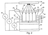
図2は、図1に示す放出器50を発展させた本発明の別の実施形態を示す図である。この実施形態では、放出器50上に電子レンズ構造51が配置され、集積放出器100が形成される。この例示的な実施形態では、薄膜層からなる導電性電極53’のスタックに第2の保護層48が含まれる。この第2の保護層48は、スペーサ層40内に穴を形成する際にエッチストップとして用いられる。スペーサ層40は、第2の保護層48上に配置され、TEOS、または酸化シリコン、窒化シリコンもしくはその組み合わせなどの処理中の熱サイクルに起因する応力を最小限に抑えることができる他の低温酸化物などの誘電体から形成されることが好ましい。スペーサ層40上には電子レンズ28が配置される。電子レンズ28は、電子16のビームを集束して、陽極30上に集束ビーム32を生成するために用いる電界34を形成することができる開口部29を有する。電界34を生成するために、供給源コンタクト12および電子レンズ28にレンズ電圧源36が接続される。供給源コンタクト12および陽極30には陽極電圧源27が接続される。陽極電圧源27は、電子16が引き寄せられるような所定の電圧に設定されることが好ましい。
FIG. 2 is a diagram showing another embodiment of the present invention in which the
図3は、本発明を組み込んだ集積放出器100の例示的な実施形態を示す平面図である。図に示すように、集積放出器は、電界の意図しない集中を防ぐために、円形であることが好ましい。しかしながら、長方形、八角形あるいは他の多角形などの他の形状を用いることもでき、このような他の形状でも本発明の精神および範囲を満たすことができる。集積放出器100は、スペーサ層40と、第2の保護層48のおそらく一部と、陰極14の放出器表面26とを露出させる開口部を有する電子レンズ28を備える。
FIG. 3 is a plan view illustrating an exemplary embodiment of an
図4は、図3の集積放出器100をIV−IVに沿って見た断面図である。この例示的な実施形態では、集積放出器100は、半導体基板10上に、好ましくはシリコン上に、また好ましくは電子の十分な供給源を提供するためにN+ドナーが高濃度にドープされたシリコン上に構成される。基板10の表面とともにあるいは表面上に、放出器隔離層58が形成される。隔離層58は、基板10上に成長したフィールド酸化膜(FOX)から形成されることが好ましい。任意により、隔離層58は、基板10上に堆積されるか、あるいは別の方法で被着される誘電体層とすることができる。隔離層58の中には、基板10から電子を放出できるようにするための開口部がある。基板10の露出した表面上には、放出層56として示される任意選択の異方性導電率層あるいはノジュール層が堆積される。基板10および放出層56は、この例示的な放出器のための電子供給源60を形成する。放出層56は、放出器表面26にわたって実質的に一様に電子を供給し、一様な放出を実現する。
4 is a cross-sectional view of the
電子供給源60上にはトンネル層20が配置され、このトンネル層は、工程汚染を最小限に抑えるためにパターニングされないことが好ましく、基板10の表面にわたって延在することが好ましい。トンネル層20の一部の上には陰極14が配置される。陰極14の上には、いずれも製造中にエッチストップとして用いられる第1の保護層54および第2の保護層48を含む導電性電極53’が配置される。導電性電極53’の中には、放出器表面26を形成する、陰極14への開口部が画定される。導電性電極53’は、第1の保護層54、第1の導電層52および第2の保護層48などの導電性薄膜材料からなる複数層から形成される。チタンあるいはモリブデンを堆積することにより、第1および第2の導電層が形成されることが好ましい。導電性電極53’上およびトンネル層の一部の上には、たとえば約5ミクロンの厚みまでのTEOSなどの誘電体から形成されるスペーサ層46が配置される。スペーサ層46の上には、第2の導電層42と、任意選択の接着層44とから形成される電子レンズ28が配置される。
A
図5および図6は、本発明の実施形態を形成するために用いられる例示的な工程のステップを示す流れ図である。図7A〜図7Tは、放出器を形成するために用いられる中間的な工程のステップの例示的な図であり、本発明の細部をさらに明確にし、理解できるようにするために示される。実際の寸法はそのような縮尺ではなく、いくつかの特徴的な部分が、その工程のステップをより明確に指示するために誇張されている。 5 and 6 are flow diagrams illustrating exemplary process steps used to form an embodiment of the present invention. 7A-7T are exemplary illustrations of the intermediate process steps used to form the emitter, and are shown to further clarify and understand the details of the present invention. The actual dimensions are not to scale, and some characteristic parts are exaggerated to more clearly indicate the process steps.
図5は、本発明の1つの例示的な実施形態を形成するための例示的な工程の流れ図である。最初に、放出器アクティブ領域が画定される。ステップ502では、基板10上に隔離層58が形成され、基板10上の開口部が画定される(図7Aを参照)。そのステップでは、基板10上にフィールド酸化層(FOX)を成長させ(図7Bを参照)、電子供給源60を形成するための開口部が画定されることが好ましい。このステップは、リセスフィールド酸化工程(酸化/エッチング/酸化)を用いて実行され、より平坦な表面を実現し、かつFOXにおけるバーズビークを低減することが好ましい。FOX厚は約4500オングストロームであることが好ましく、FOX表面から基板10の表面までの高さは約200オングストロームである。
FIG. 5 is a flowchart of an exemplary process for forming one exemplary embodiment of the present invention. Initially, the emitter active area is defined. In step 502, an
基板10のために用いることができるいくつかの異なる材料には、アルミニウム、タングステン、チタン、銅、金、タンタル、白金、イリジウム、パラジウム、ロジウム、クロム、マグネシウム、スカンジウム、イットリウム、バナジウム、ジルコニウム、ニオブ、シリコン、ベリリウム、ハフニウム、銀およびオスミウムが含まれる。基板は、任意の合金、および先に記載された基板材料からなる多層化された薄膜であってもよい。他の実現可能な基板は、ドープポリシリコン、ドープシリコン、グラファイト、金属コーティングガラス、セラミック、プラスチック、および酸化インジウムスズコーティングガラスを含む。基板材料はパターニングされても、パターニングされなくてもよい。化学機械研磨(CMP)のような従来の方法によって、所与の応用形態によって要求されるように、導電性基板の上側表面を平坦化することができる。
Several different materials that can be used for the
FOXのほかに、隔離層58は、シリコン、アルミニウム、チタン、タンタル、タングステン、ハフニウム、ジルコニウム、バナジウム、ニオブ、モリブデン、クロム、イットリウム、スカンジウム、ニッケル、コバルト、ベリリウム、マグネシウム、ダイヤモンドライクカーボン、およびそれらの組み合わせの酸化物、窒化物および酸窒化物などの他の材料の堆積あるいは熱成長によって形成されてもよい。
In addition to FOX, the
任意選択のステップ504では、基板から後に画定される放出器表面まで電子を実質的に一様に分布させるために、基板の表面および隔離層58上に放出層56(たとえば異方性導電率層あるいはノジュール層)が形成される(図7Cを参照)。放出層56は、約0.1〜2ミクロンの厚みを有するポリシリコンを用いて形成されることが好ましい。そのポリシリコンは任意選択で陽極酸化されることができるが、陽極酸化されなくてもよい。例示的なノジュール層は、ここに引用することで本明細書の一部をなすものとする、2001年10月12日に出願され、同じ譲受人に譲渡された米国特許出願第09/975,296号に記載および図示される。例示的な異方性導電率層は、ここに引用することで本明細書の一部をなすものとする、本特許出願と同時に出願され、同じ譲受人に譲渡された米国特許出願代理人整理番号第10019410−1に記載および図示される。
In
ポリシリコンが如何に形成されるかによって、異方性導電率層あるいはノジュール層のいずれかが形成されることができる。異方性導電率層は、ポリシリコンが一様な表面を有するが、Z方向およびX−Y方向において異方性の抵抗プロファイルを有するときに形成される。Z方向はポリシリコンの厚みに関連する。X−Y方向はポリシリコンの長さおよび幅寸法に関連する。ノジュール層は、電子放出を高めるために局部的な高い電界を生成する多数の突起を有するポリシリコンの層によって形成される。放出層56として異方性導電率層あるいはノジュール層を用いることにより、放出器の放出率、安定性および信頼性が高められる。
Depending on how the polysilicon is formed, either an anisotropic conductivity layer or a nodule layer can be formed. An anisotropic conductivity layer is formed when polysilicon has a uniform surface but has an anisotropic resistance profile in the Z and XY directions. The Z direction is related to the thickness of the polysilicon. The XY direction is related to the length and width dimensions of the polysilicon. The nodule layer is formed by a layer of polysilicon having a number of protrusions that generate a locally high electric field to enhance electron emission. By using an anisotropic conductivity layer or nodule layer as the
ステップ506では、基板の表面上にトンネル層20が形成される。トンネル層20は、欠陥が形成されるのを防ぐためにパターニングされないことが好ましい。任意選択の放出層56が用いられる場合には、トンネル層20はその上に堆積される(図7Dを参照)。放出層56が用いられない場合には、トンネル層は、隔離層の画定された開口部内の基板上に堆積されるか、成長するか、あるいは別の方法で被着される。トンネル層20は、ポリシリコン異方性導電率層あるいはノジュール層から約200オングストロームの厚みまで成長するRTP酸化物であることが好ましい。RTP工程のための一様な酸化膜厚および温度制御を行うために、ポリシリコン異方性導電率あるいはノジュール層以外の層のためのRTP工程を用いる場合には、非金属の放出層56が必要とされる。
In
ポリシリコンのほかに、シリコン、アルミニウム、チタン、タンタル、タングステン、ハフニウム、ジルコニウム、バナジウム、ニオブ、モリブデン、クロム、イットリウム、スカンジウム、ニッケル、コバルト、ベリリウム、マグネシウム、ダイヤモンドライクカーボン、およびそれらの組み合わせの酸化物、窒化物および酸窒化物などの他の材料の堆積あるいは熱成長を用いて、隔離層58を形成することができる。
In addition to polysilicon, oxidation of silicon, aluminum, titanium, tantalum, tungsten, hafnium, zirconium, vanadium, niobium, molybdenum, chromium, yttrium, scandium, nickel, cobalt, beryllium, magnesium, diamond-like carbon, and combinations thereof The
ステップ508では、トンネル層20の表面にわたって陰極14が被着される(図7Eを参照)。陰極14は、白金(Pt)あるいは任意選択で金(Au)を約100オングストロームまで堆積することから形成されることが好ましい。陰極14として金を用いるとき、金を50〜100オングストロームの層に、より好ましくは70オングストロームの層に堆積する前に、約10オングストロームまでタンタルを堆積することが好ましい。タンタル層を用いて、トンネル層20に対する金の接着を良好にし、かつ金がトンネル層内に入り込むのを防ぐ。トンネル層20の厚みにかかる電界を生成し、電子がトンネル層を突き抜け、脱出した電子がエネルギー放出22を形成するだけの十分な速度で陰極層14に引き寄せられるようにするために、陰極層14は電子供給源に対して正の電位をかけられるであろう。電子が陰極材料に衝突し、電子光子散乱を引き起こすことにより、光子が放出されるものと考えられ、エネルギー損失の一部は光子の生成に起因する。
In
白金あるいは金のほかに、他の用いることができる陰極層14の材料には、アルミニウム、タングステン、チタン、モリブデン、チタン、銅、銀、タンタル、イリジウム、パラジウム、ロジウム、クロム、マグネシウム、スカンジウム、イットリウム、バナジウム、ジルコニウム、ニオビウム、モリブデン、ハフニウム、オスミウム、他の耐火金属およびそれらの任意の合金あるいは多層化された薄膜が含まれる。他の用いることができる陰極表面には、ドープポリシリコン、グラファイト、あるいは導電性カーボンあるいは他の薄膜などの金属および非金属の組み合わせが含まれる。陰極層14のために選択される材料は、絶縁性の自然酸化物に酸化しないことが好ましい。
In addition to platinum or gold,
ステップ510〜516では、陰極表面に導電性電極が被着される。ステップ510では、放出器エッチストップ層、すなわち第1の保護層54が陰極層14上に被着され、後続の処理中に陰極層14が損傷あるいは汚染されるのを防ぎ、それゆえ犠牲層になる(図7Fを参照)。パッドエッチストップ層は、チタン(Ti)あるいはモリブデンを約300オングストローム〜約1500オングストロームまで堆積することにより形成されることが好ましいが、約800オングストロームであることがさらに好ましい。
In steps 510-516, a conductive electrode is deposited on the cathode surface. In
チタンあるいはモリブデンのほかに、犠牲層のための有用な他の用いることができる保護層54の材料には、アルミニウム、タングステン、モリブデン、チタン、銅、銀、タンタル、イリジウム、パラジウム、ロジウム、クロム、マグネシウム、スカンジウム、イットリウム、バナジウム、ジルコニウム、ニオブ、ハフニウム、オスミウム、およびその任意の合金が含まれる。
In addition to titanium or molybdenum, other useful
ステップ512では、放出器エッチストップ層上に第1の導電層52が被着される(図7Gを参照)。第1の導電層52は、金(Au)を約2000オングストロームまで堆積あるいはめっきすることにより形成されることが好ましい。この第1の導電層は金属トレースを形成し、第1の保護層54を通して陰極表面と電気的に接触して、電源から放出器へ電界を変化させる。
In
ステップ514では、パッドエッチストップ層、すなわち第2の保護層48が第1の導電層52上に被着される(図7Hを参照)。パッドエッチストップ層は、Tiあるいはモリブデンの約300〜約1500オングストロームの層であることが好ましいが、約800オングストロームであることがさらに好ましく、スペーサ層エッチングのためのエッチストップとして用いられ、後続のスペーサ層エッチング中に第1の導電層をスパッタリングから防ぐ。
In
ステップ516では、パッド画定フォトマスク62が、パッドエッチストップ層上に被着される(図7Iを参照)。パッド画定フォトマスク62はパターニングされ、放出器(複数可)の形状、位置、隔離および開口部(複数可)を画定する。
In
ステップ518および520では、パッドエッチストップ層および第1の導電層が、それぞれ適当なエッチャントを用いてウエットエッチングされることが好ましい(図7Jを参照)。いくつかの異なる溶液を用いることができる。たとえば、パッドエッチストップ層がTiであるとき、アンモニアおよび水の311エッチング溶液(H2O:NH4OH:H2O2=3:1:1)、希釈されたBOE、あるいは好ましくは硫酸過酸化水素エッチング(H2O2:H2SO4=1:2)を用いることができる。約800オングストロームのTiの場合、約5分間にわたって硫酸過酸化水素エッチングを用いれば十分であり好ましい。金のウエットエッチングは、約2000オングストロームの金の厚みの場合に、331の溶液(DI:Nitric:HCl=3:3:1)で、約15〜30秒のエッチング時間にわたって行われることが好ましい。
In
ステップ522では、隔離フォトマスク64が被着され、パターニングされて、放出器表面を保護し、放出器の一部ではない第1の保護層54だけを露出させる(図7Kを参照)。
In
ステップ524では、第1の保護層54および陰極層14がドライエッチングされて、各放出器を分離し、離隔させることが好ましい(図7Lを参照)。その後、隔離フォトマスク64は除去される(図7Mを参照)。
In
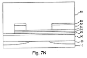
放出器が集束レンズを備えることなく用いられることになる場合には、その工程はステップ528に進み、放出器エッチストップ層、すなわち第1の保護層54が特殊な洗浄エッチングにかけられ、第1の保護層54の実質的に全てが放出器表面26から除去される(図7Tを参照)。
If the emitter is to be used without a focusing lens, the process proceeds to step 528 where the emitter etch stop layer, i.e. the first
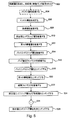
放出器が集束レンズ構造と集積されることになる場合には、第1の保護層54が陰極層14上に残され、その工程は、図6に示されるレンズ構造を形成するために用いられるステップに進む。ステップ602では、スペーサ層40が、放出器を備える処理済の基板の表面上に被着される。好ましくは低温酸化物である、いくつかの異なる誘電体薄膜が用いることができるが、その選択の過程では、薄膜間応力および薄膜間エッチング選択性が考慮されることが好ましい。スペーサ層40と処理済の基板との間の応力が大きすぎる場合には、基板が反るかもしれない(特に基板が従来の半導体シリコン基板である場合)。その反りによって、光学処理工程において誤差が生じる恐れがある。先に選択された薄膜の場合、テトラエチルオルトシリケート(TEOS)薄膜が、5ミクロン厚の薄膜の場合に、絶対値で100mPa未満の、あるいはさらに好ましくは−40〜−60mPaの範囲内の許容可能な低い応力を実現する。スペーサ層を堆積した後に、任意選択で、第2の導電層42で形成される電子レンズのための実質的に平坦な表面を形成するために、従来の平坦化装置および工程を用いて平坦化されることができる。
If the emitter is to be integrated with a focusing lens structure, the first
ステップ604では、スペーサ層40の表面上に第2の導電層42が被着される。任意選択で、最初に接着層44が被着され、誘電体層40と第2の導電層42との間の良好な界面を提供することができる(図7Oを参照)。例示的な選択は、接着層44のためには約500オングストロームの堆積したタンタルであり、第2の導電層のためには約1000オングストロームの堆積した金である。
In
ステップ606では、レンズフォトマスク66が第2の導電層42上に被着され、パターニングされて、後に放出器表面から放出される電子を集束するために用いられる開口部が画定される。
In
ステップ608では、第2の導電層が、好ましくはドライあるいはウエットエッチングを用いてエッチングされ、レンズ構造が画定され、さらに任意選択で、電子レンズと異なる電位にある陽極層を備え、静電引力を防ぐために用いられる部分シールド層が画定される(図7Pを参照)。
In
ステップ610では、バイアフォトマスク67が被着され、パターニングされて、第2の導電層内の電子レンズ開口部と実質的に位置合わせされた開口部が画定され、後にスペーサ層40を貫通するバイアをエッチングできるようにする。
In
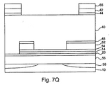
ステップ612では、スペーサ層40を貫通するバイアが第1の保護層54までエッチングされる(図7Rを参照)。第1の保護層54上で停止しながら同時に、放出器表面からスペーサ層40を除去することは、スペーサ層40としてTEOS薄膜でエッチング工程を設計する際に影響を及ぼす。放出器上にスペーサ層40の残留物があると、電子および光子の放出が遮断されるであろう。しかしながら、第1の保護層54上で停止できないと、陰極に損傷を与えるか、あるいは陰極層をかなりスパッタリングするであろう。第1の保護層54を厚くすることにより、スペーサ層エッチングマージンを大きくできるようになるが、第1の保護層の後のエッチング中に、より大きなアンダーカットが生じる恐れがある。実証的な試験は、チタンを用いるとき、アンダーカットの割合が500オングストローム厚の第1の保護層54の場合に約1ミクロンであることを示している。
In
例示的なスペーサ層40プラズマエッチング工程は、900ワットのRF電力、300mTorrの圧力、電極ギャップ1.3cm、および20sccmCHF3+20sccmCF4+275sccmArのガス流というパラメータで行われる。TEOSの場合のエッチング速度は約4550オングストローム/分である。このエッチングは、第1の保護層のために用いられるフォトレジストおよびチタンの両方に対してエッチング選択性を与える。選択性の比はレジストの場合には約7:1であり、チタンの場合には20:1である。他のエッチング工程を用いることができ、それでも本発明は精神および範囲を満たすことができる。スペーサ層および保護層のためのエッチング選択性の比は10:1よりも大きいことが好ましく、10:1〜50:1の範囲内にあることがさらに好ましい。
An
任意選択のステップ614では、基板10の背面に背面導電層が被着され、供給源コンタクト12が形成される。任意選択で、供給源コンタクト12を被着する前に、基板10の背面にコンタクト接着層68が被着されることができる(図7Sを参照)。基板を接触させる別の方法は、上側表面上にドープされた基板コンタクトを用いることを含む。基板を接触させるいくつかの他の方法が当業者には知られている。
In
ステップ616では、第1の保護層のエッチングを実行して、図5のステップ528において第1の保護層54の実質的に全ての残留物を除去し、放出器表面26を清浄にするために、処理済の基板が戻される(図7Tを参照)。先に記載されたように、このエッチングステップは、欠陥が放出器表面26上に形成されるのを防ぐために、できる限り完全に第1の保護層をきれいにすることである。複数の異なった溶液を用いることができる。パッドエッチストップ層がTiであるとき、アンモニアおよび水の311エッチング溶液(H2O:NH4OH:H2O2=3:1:1)、希釈されたBOE、あるいは好ましくは硫酸過酸化水素エッチング(H2O2:H2SO4=1:2)を用いることができる。約800オングストロームのTiの場合、エッチングの浴寿命および温度が制御下で保持されるなら、5分間だけ硫酸過酸化水素エッチングを用いれば十分である。
In
図8は、アレイとして配列され、放出器制御回路72によって制御される1つまたは複数の集積放出器100を有する集積回路70の形の本発明の例示的な実施形態である。放出器制御回路は、各集積放出器100を個別に制御できるようにする。トンネル層20の厚みを制御することにより、集積放出器のターンオン電圧は、集積回路が従来のCMOS、BiCMOSあるいはカスタムCMOS/HVCMOS回路で形成されることができるように選択されることができる。従来の半導体工程を用いることができるようにすることにより、コストを下げ、放出器および回路の組み合わせを量産できるようになる。
FIG. 8 is an exemplary embodiment of the present invention in the form of an
図9は、集積放出器100の別の実施形態であり、その集積放出器は、好ましくは電子16が集束されたビーム32になされるときに、その電子16によって影響を及ぼされるディスプレイ画面あるいはプログラマブル媒体表面のような陽極表面76を備える。陽極表面16は、電子レンズ28から所定の距離74に保持される。この実施形態では、放出層56として異方性導電率あるいはノジュール層を用いることなく形成される集積放出器が示されるが、任意選択でそれを備えることができる。
FIG. 9 is another embodiment of an
図10は、概念的なディスプレイ80における本発明の別の実施形態である。そのディスプレイは好ましくはピクセル82のアレイから構成され、そのピクセルはさらに赤色、青色および緑色の順序で配列されるが、単色にすることもできるであろう。ピクセル82はディスプレイ画面84上に形成される。放出器アレイ78は、電子放出16を生成するように個別に制御される、長方形のフラット放出器として示される、本発明を組み込む1つまたは複数の集積電子放出器100を有する。電子放出16は、アルミニウム、金あるいは他の金属または半導体薄膜などの材料の導電層から形成されることが好ましい電子レンズ28を用いて集束される。電子レンズ28はディスプレイ画面84と放出アレイ78との間に配置される。通常、ディスプレイ画面84は、500ボルトより大きな電位、たとえば700ボルトの電位に保持され、電子放出16を引き寄せる。電子レンズ28は、ディスプレイ画面84上にあるピクセル82上のスポットサイズに電子放出16を集束するレンズ開口部86を有する。電子レンズ28は、−20ボルトのような、放出器表面よりも高い電位に保持され、レンズ開口部86の周囲および内部に電界を生成し、電子レンズを形成する。ディスプレイ画面84、放出器アレイ78および電子レンズ28の間の電位差が静電引力を生成し、それによりディスプレイ画面84が電子レンズ28および放出器アレイ78に引き寄せられるようになる。この静電引力を最小限に抑えるために、ディスプレイ画面84と電子レンズ28との間に任意選択のシールド層(図示せず)が配置される。シールド層は、好ましくはレンズ開口部86と同じ形状およびサイズのシールド開口部を有し、電子放出16がシールド層を通ってディスプレイ画面84まで通過できるようにする。
FIG. 10 is another embodiment of the present invention in a
図11は、集積されたディスプレイ装置90の形をとる本発明の別の実施形態である。集積ディスプレイ装置90は基板10、好ましくはシリコン基板であるが、任意選択で別のタイプの半導体あるいは別法ではガラス基板から形成される。そのような材料からなるいくつかの用いることができる基板が当業者には知られている。この例示的な設計における基板10は、基板10上に形成される薄膜層88のスタックを有する。薄膜層88のスタックは、本発明を組み込む集積放出器100のアレイを含むことが好ましい。ここでは、集積放出器100はピクセル蛍光体82毎にフラット放出器として示されるが、ピクセル蛍光体82毎に2つ以上のフラット放出器が存在することもできる。各集積放出器100は、薄膜層88のスタック内に埋め込まれ、画面陽極92と基板10との間に配置される電子レンズ28で集束される電子放出16を生成することができる。画面84は、スペーサ94によって陽極レンズ距離74だけ、薄膜層88のスタックから離間して配置される。スペーサ94は、当業者に知られているいくつかの任意選択の材料から選択され、形成される。またスペーサ94は気密封止も与えることが好ましいが、任意選択で、集積ディスプレイ装置90の周囲に別のシール96あるいは接着剤を加えることができる。
FIG. 11 is another embodiment of the present invention in the form of an
図12Aおよび図12Bは概念的な大容量記憶装置110において用いられる本発明の別の実施形態である。概念的な大容量記憶装置110は、好ましくは縦方向のスタックとして配列される3つの異なる基板を有するものとして例示される。基板10は、集積放出器100および電子レンズ28を含む1つの表面上に形成される薄膜層88のスタックを有する。集積放出器100および電子レンズ28は集束されたビーム32を生成し、そのビームは、基板10とステータ基板108との間に配置されるロータ基板106上にある媒体表面102上に、小さなスポットサイズ、好ましくは40ナノメートル未満のスポットサイズ、例えば約10ナノメートルのスポットサイズを生成する。ロータ基板108上の媒体表面102は、集束されたビーム32のエネルギーによって影響を及ぼされる相変化材料から形成されることが好ましい。相変化材料は、高い電力レベルの集束されたビーム32を利用し、集束されたビーム32の電力レベルを急激に減少させることにより、結晶状態から非晶質状態126に変化することができる。相変化材料は、高い電力レベルの集束されたビーム32を利用し、媒体表面が結晶状態にアニールするだけの時間があるように、その電力レベルを徐々に減少させることにより、非晶質状態126から結晶状態に変化することができる。例示的な材料は、テルル化ゲルマニウム(GeTe)およびGeTeを基にする3元合金である。
12A and 12B are another embodiment of the present invention used in the conceptual
いくつかの他の相変化材料が当業者に知られており、本発明の範囲および精神から逸脱することなく代わりに用いられることができる。他の好ましい相変化材料のいくつかの例には、GaSb、InSb、InSe、Sb2Te3、Ge2Sb2Te5、InSbTe、GaSeTe、SnSb2Te4、InSbGe、AgInSbTe、(GeSn)SbTe、GeSb(SeTe)、Te81Ge15Sb2S2およびGeSbTeなどのカルコゲニド合金がある。 Several other phase change materials are known to those skilled in the art and can be used instead without departing from the scope and spirit of the present invention. Some examples of other preferred phase change materials include GaSb, InSb, InSe, Sb 2 Te 3 , Ge 2 Sb 2 Te 5 , InSbTe, GaSeTe, SnSb 2 Te 4 , InSbGe, AgInSbTe, (GeSn) SbTe, There are chalcogenide alloys such as GeSb (SeTe), Te 81 Ge 15 Sb 2 S 2 and GeSbTe.
ロータ基板106およびステータ基板108は、ロータ基板106が第1および好ましくは第2の方向に動くことができるようにし、単一の集積放出器100が媒体表面上のいくつかの位置において読出しおよび書込みを行うことができるようにするための電子回路を含む。
The
媒体表面から読出しを行うために、低いエネルギーの集束されたビーム32を媒体102上の媒体表面に衝当し、それにより媒体基板106の中に電子が流れるようになり、リーダ回路104がそれを検出する。検出される電流の量は、集束されたビーム32によって衝当される媒体表面の状態、すなわち非晶質状態あるいは結晶状態による。例示的なリーダ回路104の動作が、第1のコンタクト128が媒体表面102に接続され、第2のコンタクト129が媒体基板106に接続されるものとして示される。基板内を流れる電流は、増幅器130によって電圧に変換され、リーダ出力132が生成される。他のリーダ回路が当業者には知られており、本発明の範囲および精神から逸脱することなく代わりに用いられることができる。
In order to read from the media surface, a low energy focused
図13は、例示的な集積大容量記憶装置120によって示される本発明の別の実施形態である。集積大容量記憶装置120は3つの基板、すなわち基板10と、ロータ基板106と、ステータ基板108とを備える。ロータ基板106は、静電回路104を用いて好ましくは第1および第2の方向に、好ましくはステップモータタイプの関数で動くことができる、基板の一部の上にある少なくとも1つの媒体表面102を有する。移動可能な媒体表面102は、好ましくはロータ基板をエッチングすることによって形成されるばね114によって支持される。当業者は、移動可能な媒体表面102を形成するためのいくつかの異なる微小電気機械システム(MEMS)構造を知っている。
FIG. 13 is another embodiment of the present invention illustrated by an exemplary integrated
ステータ基板108とロータ基板106との間の電気的な接触はコンタクト118によって実行される。ボンディングシール116がロータ基板106をステータ基板108に取り付けることが好ましく、その内部を封止して、集積大容量記憶装置120内の真空状態を保持することが好ましい。またロータ基板106は、好ましくは気密シールでもあるスペーサ124を用いて基板10に取り付けられる。任意選択で、スペーサ124の代わりに、あるいはスペーサ124とともに別のシール122を用いて、基板10をロータ基板106に接着および/または封止することができる。
Electrical contact between the
基板10は、従来の半導体装置を用いて被着されることが好ましい薄膜層88のスタックを含む。薄膜層88のスタックは本発明を組み込む1組の集積放出器100を備え、その集積放出器100は、電界34を生成する電子レンズ28を用いて集束され、その電界34が、媒体表面102上に、好ましくは40ナノメートル未満の、さらに好ましくは10ナノメートル未満のスポットサイズまでの集束されたビーム32を生成する。電子レンズ28は、約7.2マイクロメートルのレンズ開口部を有することが好ましい。基板10とロータ基板106との間の空間は、集積放出器100から放出される電子がガスあるいは他の粒子と衝突し、それが集積放出器100に損傷を与えるようになるのを防ぐために、好ましくは10-3Torr未満まで空気を抜かれることが好ましい。集積放出器100は第1の電位に保持され、好ましくはトンネル技法によって電子を生成する。第1の電位は約25ボルト未満であることが好ましい。電子レンズ28は第2の電位に、好ましくはグランドに対して約0Vに保持され、電子を集束するために用いられる電界34を生成する。記憶媒体102は好ましくは500ボルトよりも高い第3の電位に、たとえば約700ボルトの電位に保持され、集積放出器100から放出される電子を引き寄せることが好ましい。電子レンズ28は、集積放出器100から第1の距離、たとえば約5マイクロメートルだけ離隔されることが好ましい。
図14は、数例を挙げると、コンピュータシステム、テレビゲーム、インターネット機器、端末、MP3プレーヤあるいは携帯情報端末のような電子装置140の例示的なブロック図である。電子装置140は、インテル・ペンティアム(登録商標)プロセッサあるいは互換性のあるプロセッサなどのマイクロプロセッサ134を備えるが、他のプロセッサも存在し、当業者には知られている。マイクロプロセッサ134は、データおよび/または入力/出力機能を制御するためにマイクロプロセッサ134によって用いられるコンピュータ実行可能コマンドを保持することができるコンピュータ読取り可能メモリを含むメモリデバイス136に接続される。メモリ136は、マイクロプロセッサ134によって操作されるデータも格納することができる。マイクロプロセッサ134は、記憶装置110あるいはディスプレイ装置80のいずれか、または両方にも接続される。記憶装置110およびディスプレイ装置80は、電界放出デバイスを示す、先に説明された図面および本文に例示されるような、本発明の一実施形態を含む。
FIG. 14 is an exemplary block diagram of an
図15は、放出器50のアレイ78あるいは任意選択で集積放出器100のいずれかを用いて、集束ビーム32を生成するための光学レンズ98を用いて集束される画像を形成する光学ディスプレイ装置150を示す本発明の別の実施形態である。放出器50は光子18を生成し、電子16(図示せず)も生成する。光学レンズ98の放出器50に面する側にある酸化インジウムスズなどの透明導体99が電子を捕捉する。透明導体99の1つの目的は、放出される電子がレンズ上に収集されるのを防ぐとともに、高い静電界を生成しながら、光子18が通過できるようにすることである。
FIG. 15 illustrates an
本発明が上記の好ましい実施形態および代替の実施形態を参照しながら詳細に図示および説明されてきたが、添付の特許請求の範囲において規定された本発明の精神および範囲から逸脱することなく、数多くの変形ができることは当業者に理解されよう。本発明のこの記述は、本明細書に記載される構成要素の全ての新規かつ非自明な組み合わせを含むものと理解されるべきであり、特許請求の範囲は、これらの構成要素の任意の新規かつ非自明な組み合わせに対して本出願または将来の出願において提示されるかもしれない。上記の実施形態は例示であり、本出願あるいは将来の出願において請求されるかもしれない全ての実現可能な組み合わせに対して、特徴的な部分あるいは構成要素が単一であることは不可欠ではない。請求項が、その相当する部分の「1つ」あるいは「第1」の構成要素を列挙する場合、そのような請求項は、1つまたは複数のそのような構成要素を組み込むことも含まれると理解されるべきであり、2つ以上のそのような構成要素を要求も排除もされない。 While the invention has been illustrated and described in detail with reference to the preferred and alternative embodiments described above, numerous changes can be made without departing from the spirit and scope of the invention as defined in the appended claims. Those skilled in the art will appreciate that these variations are possible. This description of the invention should be understood to include all novel and non-obvious combinations of the components described herein, and the claims are intended to cover any novel of these components. And may be presented in this or future applications for non-obvious combinations. The above embodiments are exemplary, and it is not essential for a single feature or component for all possible combinations that may be claimed in this or a future application. Where a claim enumerates “one” or “first” component of the corresponding part, such claim also includes the incorporation of one or more such component It should be understood that two or more such components are not required or excluded.
Claims (20)
該電子供給源の上に配置されたトンネル層(20)と、
該トンネル層の上に配置された陰極層(14)と、
該陰極層の上に配置された保護層(54)を含む導電性材料の複数層(52、54)を有する導電性電極(53)と
を含んでなる放出器(50、100)であって、前記導電性電極が開口部(26)を画定するようにエッチングされており、それにより前記陰極層の一部が露出されている放出器。 An electron source (60);
A tunnel layer (20) disposed on the electron source;
A cathode layer (14) disposed on the tunnel layer;
An emitter (50, 100) comprising: a conductive electrode (53) having a plurality of layers (52, 54) of conductive material including a protective layer (54) disposed on the cathode layer; An emitter wherein the conductive electrode is etched to define an opening (26), thereby exposing a portion of the cathode layer.
前記第1の導電性電極上に配置され、かつ前記第1の導電性電極の前記開口部と実質的に位置合わせされる開口部を画定する第2の保護層(48)と、
該第2の保護層上に配置され、かつ前記第1の導電性電極の前記開口部と実質的に位置合わせされる開口部を画定するスペーサ層(40)と、
該スペーサ層上に配置され、かつ前記導電性電極の前記開口部と実質的に位置合わせされる開口部(29)を画定する第2の導電性電極(28)と
を含んでなる請求項1に記載の放出器。 The protective layer (54) is a first protective layer, the conductive electrode (53) is a first conductive electrode, and the emitter is further
A second protective layer (48) disposed on the first conductive electrode and defining an opening substantially aligned with the opening of the first conductive electrode;
A spacer layer (40) disposed on the second protective layer and defining an opening substantially aligned with the opening of the first conductive electrode;
A second conductive electrode (28) disposed on the spacer layer and defining an opening (29) substantially aligned with the opening of the conductive electrode. The emitter as described in.
該基板上に配置される請求項1に記載の少なくとも1つの放出器(50、100)と、
該少なくとも1つの放出器を動作させるために前記放出器とともに前記基板上に形成される回路(72)と
を含んでなる集積回路(70)。 A substrate (10);
At least one emitter (50, 100) according to claim 1 disposed on the substrate;
An integrated circuit (70) comprising: a circuit (72) formed on the substrate with the emitter to operate the at least one emitter.
前記放出されたエネルギーを受け取り、前記放出されたエネルギーを受け取るのに応答して少なくとも第1の作用を生み出し、前記放出されたエネルギーを受け取らないのに応答して第2の作用を生み出すための陽極構造(30、76、84、102)と
を含んでなる電子デバイス(80、90、110、134、136、140)。 The emitter (50, 100) of claim 1 for releasing energy (22);
An anode for receiving the emitted energy, producing at least a first action in response to receiving the emitted energy, and producing a second action in response to not receiving the emitted energy An electronic device (80, 90, 110, 134, 136, 140) comprising: a structure (30, 76, 84, 102).
前記放出表面から所定の距離に配置される電子レンズ(28)と、
前記陰極層と前記電子レンズとの間に配置される少なくとも1つの犠牲層(54、48)であって、該少なくとも1つの犠牲層が前記放出表面と実質的に位置合わせされる開口部を有し、また前記少なくとも1つの犠牲層がチタンあるいはモリブデンである、少なくとも1つの犠牲層と
を含んでなる放出器(100)。 A cathode layer (14) having an emission surface (26);
An electron lens (28) disposed at a predetermined distance from the emission surface;
At least one sacrificial layer (54, 48) disposed between the cathode layer and the electron lens having an opening in which the at least one sacrificial layer is substantially aligned with the emission surface. And at least one sacrificial layer, wherein the at least one sacrificial layer is titanium or molybdenum.
該電子供給源の上に形成されるトンネル層(20)と、
該トンネル層上に形成される陰極層(14)と、
該陰極層上に配置される導電性保護層(54)と
を含んでなる放出器(50、100)であって、前記導電性保護層が開口部を画定するようにエッチングされており、それにより電子放出(22)のための前記陰極層の一部が露出している放出器。 An electron source (60);
A tunnel layer (20) formed on the electron source;
A cathode layer (14) formed on the tunnel layer;
An emitter (50, 100) comprising a conductive protective layer (54) disposed on the cathode layer, the conductive protective layer being etched to define an opening; An emitter in which a part of the cathode layer for electron emission (22) is exposed.
前記可視光源を集束するためのレンズ(98)であって、該レンズは、前記放出器から放出される電子(16)を捕捉するために透明な導電性表面(99)がコーティングされているレンズと
を含んでなるディスプレイ装置(150)。 An integrated circuit (78) comprising the emitter (50) according to claim 11, wherein the emitter generates a visible light source;
A lens (98) for focusing the visible light source, which is coated with a transparent conductive surface (99) to capture electrons (16) emitted from the emitter A display device (150) comprising:
該基板上に形成され、その中に第1の開口部(60)が画定される絶縁体層(58)と、
該絶縁体層および前記第1の開口部上に配置され、前記基板と接触する放出層(56)と、
該放出層上に形成されるトンネル層(20)と、
該トンネル層上に配置される陰極層(14)であって、前記トンネル層上にある該陰極層の部分が電子放出表面である陰極層と、
該陰極層上に配置され、前記第1の開口部と実質的に位置合わせされる第2の開口部(26)を画定する導電性保護層(54)と
を含んでなる放出器(50、100)。 A substrate (10);
An insulator layer (58) formed on the substrate and defining a first opening (60) therein;
An emission layer (56) disposed on the insulator layer and the first opening and in contact with the substrate;
A tunnel layer (20) formed on the emission layer;
A cathode layer (14) disposed on the tunnel layer, wherein a portion of the cathode layer on the tunnel layer is an electron emission surface;
An emitter comprising a conductive protective layer (54) disposed on the cathode layer and defining a second opening (26) substantially aligned with the first opening. 100).
前記陰極放出表面上に導電性の保護層を被着するステップ(510)と、
前記保護層上に電子レンズ構造を形成するステップ(602〜612)と、
前記保護層をエッチングして、前記陰極放出表面を露出させるステップ(528)と
を含んでなる方法。 A method for forming an emitter (50, 100) having a cathode emitting surface (26) comprising:
Depositing a conductive protective layer on the cathode emitting surface (510);
Forming an electron lens structure on the protective layer (602 to 612);
Etching the protective layer to expose the cathode emitting surface (528).
The method of claim 17, wherein the protective layer (54) is etched with hydrogen peroxide sulfate or ammonia and water to form the exposed cathode emitting surface.
Applications Claiming Priority (2)
| Application Number | Priority Date | Filing Date | Title |
|---|---|---|---|
| US10/066,149 US6703252B2 (en) | 2002-01-31 | 2002-01-31 | Method of manufacturing an emitter |
| PCT/US2003/002955 WO2003065425A2 (en) | 2002-01-31 | 2003-01-30 | Emitter and method of making |
Publications (2)
| Publication Number | Publication Date |
|---|---|
| JP2005516368A true JP2005516368A (en) | 2005-06-02 |
| JP2005516368A5 JP2005516368A5 (en) | 2006-03-16 |
Family
ID=27610439
Family Applications (1)
| Application Number | Title | Priority Date | Filing Date |
|---|---|---|---|
| JP2003564919A Withdrawn JP2005516368A (en) | 2002-01-31 | 2003-01-30 | Ejector and manufacturing method thereof |
Country Status (7)
| Country | Link |
|---|---|
| US (3) | US6703252B2 (en) |
| EP (1) | EP1470566A2 (en) |
| JP (1) | JP2005516368A (en) |
| AU (1) | AU2003208921A1 (en) |
| NO (1) | NO20043538L (en) |
| TW (1) | TWI277116B (en) |
| WO (1) | WO2003065425A2 (en) |
Families Citing this family (33)
| Publication number | Priority date | Publication date | Assignee | Title |
|---|---|---|---|---|
| US6911768B2 (en) * | 2001-04-30 | 2005-06-28 | Hewlett-Packard Development Company, L.P. | Tunneling emitter with nanohole openings |
| US7049034B2 (en) * | 2003-09-09 | 2006-05-23 | Photronics, Inc. | Photomask having an internal substantially transparent etch stop layer |
| KR100513727B1 (en) * | 2003-02-12 | 2005-09-08 | 삼성에스디아이 주식회사 | Manufacturing method of a field emission device |
| US20070003472A1 (en) * | 2003-03-24 | 2007-01-04 | Tolt Zhidan L | Electron emitting composite based on regulated nano-structures and a cold electron source using the composite |
| WO2004098684A2 (en) * | 2003-05-08 | 2004-11-18 | Novo Nordisk A/S | Skin mountable injection device with a detachable needle insertion actuation |
| DE602004013140T2 (en) * | 2003-05-08 | 2009-07-02 | Novo Nordisk A/S | INTERNAL NEEDLE INTAKE DEVICE |
| EP1475113A1 (en) * | 2003-05-08 | 2004-11-10 | Novo Nordisk A/S | External needle inserter |
| US6987688B2 (en) * | 2003-06-11 | 2006-01-17 | Ovonyx, Inc. | Die customization using programmable resistance memory elements |
| JP4545397B2 (en) * | 2003-06-19 | 2010-09-15 | 株式会社 日立ディスプレイズ | Image display device |
| EP1502613A1 (en) * | 2003-08-01 | 2005-02-02 | Novo Nordisk A/S | Needle device with retraction means |
| US20050051764A1 (en) * | 2003-09-04 | 2005-03-10 | Huei-Pei Kuo | Anodizing process for improving electron emission in electronic devices |
| KR20060099520A (en) * | 2003-10-21 | 2006-09-19 | 노보 노르디스크 에이/에스 | Medical skin mountable device |
| US7459839B2 (en) * | 2003-12-05 | 2008-12-02 | Zhidan Li Tolt | Low voltage electron source with self aligned gate apertures, and luminous display using the electron source |
| EP1732626A1 (en) * | 2004-03-30 | 2006-12-20 | Novo Nordisk A/S | Actuator system comprising lever mechanism |
| US20060051681A1 (en) * | 2004-09-08 | 2006-03-09 | Phototronics, Inc. 15 Secor Road P.O. Box 5226 Brookfield, Conecticut | Method of repairing a photomask having an internal etch stop layer |
| JP2006080046A (en) * | 2004-09-13 | 2006-03-23 | Ngk Insulators Ltd | Electron emitting device |
| US20090012472A1 (en) * | 2004-09-22 | 2009-01-08 | Novo Nordisk A/S | Medical Device with Cannula Inserter |
| CN101027095B (en) * | 2004-09-22 | 2010-09-29 | 诺和诺德公司 | Medical device with cannula inserter |
| DE602005016298D1 (en) * | 2004-12-06 | 2009-10-08 | Novo Nordisk As | VENTILATED DEVICE AT THE SKIN |
| WO2006077263A1 (en) * | 2005-01-24 | 2006-07-27 | Novo Nordisk A/S | Transcutaneous device assembly |
| US20080167641A1 (en) * | 2005-05-13 | 2008-07-10 | Novo Nordisk A/S | Medical Device Adapted To Detect Disengagement Of A Transcutaneous Device |
| US7786662B2 (en) | 2005-05-19 | 2010-08-31 | Texas Instruments Incorporated | Display using a movable electron field emitter and method of manufacture thereof |
| US20070096621A1 (en) * | 2005-10-31 | 2007-05-03 | Sang-Ho Jeon | Electron emission display |
| WO2007104756A1 (en) * | 2006-03-13 | 2007-09-20 | Novo Nordisk A/S | Medical system comprising dual purpose communication means |
| US9173992B2 (en) * | 2006-03-13 | 2015-11-03 | Novo Nordisk A/S | Secure pairing of electronic devices using dual means of communication |
| EP2012852A1 (en) * | 2006-04-26 | 2009-01-14 | Novo Nordisk A/S | Skin-mountable device in packaging comprising coated seal member |
| CN101460207B (en) * | 2006-06-06 | 2012-03-21 | 诺沃-诺迪斯克有限公司 | Assembly comprising skin-mountable device and packaging therefore |
| CN101192494B (en) | 2006-11-24 | 2010-09-29 | 清华大学 | Electron emission element preparation method |
| CN101192490B (en) | 2006-11-24 | 2010-09-29 | 清华大学 | Surface conductive electronic emission element and electronic source applying same |
| WO2008107467A1 (en) * | 2007-03-06 | 2008-09-12 | Novo Nordisk A/S | Pump assembly comprising actuator system |
| CN101888859B (en) * | 2007-10-31 | 2014-09-17 | 诺沃-诺迪斯克有限公司 | Non-porous material as sterilization barrier |
| WO2009086084A1 (en) * | 2007-12-19 | 2009-07-09 | Contour Semiconductor, Inc. | Field-emitter-based memory array with phase-change storage devices |
| KR101615634B1 (en) * | 2010-02-09 | 2016-04-26 | 삼성전자주식회사 | Terahertz raidation source and method of manufacturing electron emitter |
Family Cites Families (28)
| Publication number | Priority date | Publication date | Assignee | Title |
|---|---|---|---|---|
| US5142A (en) * | 1847-06-05 | Rotary steam-engine | ||
| DE3752249T2 (en) | 1986-07-04 | 1999-07-08 | Canon Kk | Electron emitting device |
| US4760567A (en) * | 1986-08-11 | 1988-07-26 | Electron Beam Memories | Electron beam memory system with ultra-compact, high current density electron gun |
| US4923421A (en) | 1988-07-06 | 1990-05-08 | Innovative Display Development Partners | Method for providing polyimide spacers in a field emission panel display |
| JPH02306520A (en) * | 1989-05-19 | 1990-12-19 | Matsushita Electric Ind Co Ltd | Electron emitting element |
| US5142184B1 (en) | 1990-02-09 | 1995-11-21 | Motorola Inc | Cold cathode field emission device with integral emitter ballasting |
| US5086017A (en) * | 1991-03-21 | 1992-02-04 | Industrial Technology Research Institute | Self aligned silicide process for gate/runner without extra masking |
| EP0532019B1 (en) | 1991-09-13 | 1997-12-29 | Canon Kabushiki Kaisha | Semiconductor electron emission device |
| US5374844A (en) | 1993-03-25 | 1994-12-20 | Micrel, Inc. | Bipolar transistor structure using ballast resistor |
| US5528103A (en) | 1994-01-31 | 1996-06-18 | Silicon Video Corporation | Field emitter with focusing ridges situated to sides of gate |
| US5473218A (en) * | 1994-05-31 | 1995-12-05 | Motorola, Inc. | Diamond cold cathode using patterned metal for electron emission control |
| US5541466A (en) | 1994-11-18 | 1996-07-30 | Texas Instruments Incorporated | Cluster arrangement of field emission microtips on ballast layer |
| US5557596A (en) | 1995-03-20 | 1996-09-17 | Gibson; Gary | Ultra-high density storage device |
| US5578900A (en) * | 1995-11-01 | 1996-11-26 | Industrial Technology Research Institute | Built in ion pump for field emission display |
| JPH10308166A (en) | 1997-03-04 | 1998-11-17 | Pioneer Electron Corp | Electron emission element and display device using the same |
| US6033924A (en) | 1997-07-25 | 2000-03-07 | Motorola, Inc. | Method for fabricating a field emission device |
| TW391022B (en) * | 1997-10-29 | 2000-05-21 | Mitsubishi Rayon Co | Field emission electron source, method of producing the same, and use of the same |
| US6010918A (en) * | 1998-02-10 | 2000-01-04 | Fed Corporation | Gate electrode structure for field emission devices and method of making |
| US6303504B1 (en) * | 1998-02-26 | 2001-10-16 | Vlsi Technology, Inc. | Method of improving process robustness of nickel salicide in semiconductors |
| US6011356A (en) | 1998-04-30 | 2000-01-04 | St. Clair Intellectual Property Consultants, Inc. | Flat surface emitter for use in field emission display devices |
| JP2000182511A (en) | 1998-12-14 | 2000-06-30 | Yamaha Corp | Manufacture of field emission type element |
| JP2000331595A (en) * | 1999-05-18 | 2000-11-30 | Nikon Corp | Thin-film cold cathode and its manufacture |
| US6360821B1 (en) * | 1999-05-20 | 2002-03-26 | Tiw Corporation | Combination whipstock and anchor assembly |
| BR0001211C1 (en) | 2000-04-13 | 2002-03-05 | Inst Nac De Tecnologia Da Info | Sending plate structure for fed |
| KR100899588B1 (en) * | 2000-10-26 | 2009-05-27 | 오우크-미츠이, 인크 . | Use of metallic treatment on copper foil to produce fine lines and replace oxide process in printed circuit board production |
| US6781146B2 (en) * | 2001-04-30 | 2004-08-24 | Hewlett-Packard Development Company, L.P. | Annealed tunneling emitter |
| US6558968B1 (en) * | 2001-10-31 | 2003-05-06 | Hewlett-Packard Development Company | Method of making an emitter with variable density photoresist layer |
| US6835947B2 (en) * | 2002-01-31 | 2004-12-28 | Hewlett-Packard Development Company, L.P. | Emitter and method of making |
-
2002
- 2002-01-31 US US10/066,149 patent/US6703252B2/en not_active Expired - Lifetime
- 2002-11-29 TW TW091134879A patent/TWI277116B/en not_active IP Right Cessation
-
2003
- 2003-01-30 AU AU2003208921A patent/AU2003208921A1/en not_active Abandoned
- 2003-01-30 WO PCT/US2003/002955 patent/WO2003065425A2/en not_active Application Discontinuation
- 2003-01-30 JP JP2003564919A patent/JP2005516368A/en not_active Withdrawn
- 2003-01-30 EP EP03707644A patent/EP1470566A2/en not_active Withdrawn
- 2003-10-15 US US10/686,965 patent/US6933517B2/en not_active Expired - Lifetime
- 2003-10-15 US US10/688,731 patent/US7049158B2/en not_active Expired - Lifetime
-
2004
- 2004-08-25 NO NO20043538A patent/NO20043538L/en not_active Application Discontinuation
Also Published As
| Publication number | Publication date |
|---|---|
| NO20043538L (en) | 2004-08-25 |
| WO2003065425A3 (en) | 2004-04-01 |
| TW200302499A (en) | 2003-08-01 |
| EP1470566A2 (en) | 2004-10-27 |
| US7049158B2 (en) | 2006-05-23 |
| TWI277116B (en) | 2007-03-21 |
| US20040130251A1 (en) | 2004-07-08 |
| WO2003065425A2 (en) | 2003-08-07 |
| US6703252B2 (en) | 2004-03-09 |
| US6933517B2 (en) | 2005-08-23 |
| US20030143788A1 (en) | 2003-07-31 |
| US20040087240A1 (en) | 2004-05-06 |
| AU2003208921A1 (en) | 2003-09-02 |
Similar Documents
| Publication | Publication Date | Title |
|---|---|---|
| JP2005516368A (en) | Ejector and manufacturing method thereof | |
| US7118982B2 (en) | Emitter and method of making | |
| JP2003234061A (en) | Improved electron emitting element for data storage application and its manufacturing method | |
| JP2005135930A (en) | Tunneling emitter and forming method | |
| US6741016B2 (en) | Focusing lens for electron emitter with shield layer | |
| JP2003308776A (en) | Electronic device having getter used as circuit element | |
| JP2005502159A (en) | Tunnel emitter | |
| JP2005515584A (en) | Silicon-based dielectric tunnel emitter | |
| US6852554B2 (en) | Emission layer formed by rapid thermal formation process | |
| US7148621B2 (en) | Integrated focusing emitter | |
| JP2004221079A (en) | Electronic device equipped with wide lens for obtaining small spot size of emission |
Legal Events
| Date | Code | Title | Description |
|---|---|---|---|
| A521 | Request for written amendment filed |
Free format text: JAPANESE INTERMEDIATE CODE: A523 Effective date: 20060124 |
|
| A621 | Written request for application examination |
Free format text: JAPANESE INTERMEDIATE CODE: A621 Effective date: 20060124 |
|
| A761 | Written withdrawal of application |
Free format text: JAPANESE INTERMEDIATE CODE: A761 Effective date: 20070126 |