JP2005292925A - Memory controller, flash memory system, and control method for flash memory - Google Patents
Memory controller, flash memory system, and control method for flash memory Download PDFInfo
- Publication number
- JP2005292925A JP2005292925A JP2004103307A JP2004103307A JP2005292925A JP 2005292925 A JP2005292925 A JP 2005292925A JP 2004103307 A JP2004103307 A JP 2004103307A JP 2004103307 A JP2004103307 A JP 2004103307A JP 2005292925 A JP2005292925 A JP 2005292925A
- Authority
- JP
- Japan
- Prior art keywords
- data
- flash memory
- user data
- capacity
- additional data
- Prior art date
- Legal status (The legal status is an assumption and is not a legal conclusion. Google has not performed a legal analysis and makes no representation as to the accuracy of the status listed.)
- Pending
Links
Images
Abstract
Description
本発明は、メモリコントローラ及びメモリコントローラを備えるフラッシュメモリシステム、並びに、フラッシュメモリの制御方法に関する。 The present invention relates to a memory controller, a flash memory system including the memory controller, and a flash memory control method.
近年、メモリーカードやシリコンディスクといったメモリシステムにて使用される半導体メモリに、フラッシュメモリが広く採用されている。フラッシュメモリは、不揮発性メモリの一種である。フラッシュメモリに格納されたデータは、電力が供給されていないときでも保持されていることが要求される。 In recent years, flash memories have been widely adopted as semiconductor memories used in memory systems such as memory cards and silicon disks. A flash memory is a kind of nonvolatile memory. Data stored in the flash memory is required to be retained even when power is not supplied.
NAND型フラッシュメモリは、上記のメモリシステムで特に多く用いられるフラッシュメモリの一種である。NAND型フラッシュメモリに含まれている複数のメモリセルのそれぞれは、他のメモリセルとは独立して、論理値“1”を示すデータが格納されている消去状態から、論理値“0”を示すデータが格納されている書込状態へと変化することができる。これとは対照的に、書込状態から消去状態へと変化するときには、各メモリセルは他のメモリセルと独立して変化することができない。このときには、ブロックと称される予め定められた数のメモリセルが、全て同時に消去状態になる。 A NAND flash memory is a type of flash memory that is particularly frequently used in the above memory system. Each of the plurality of memory cells included in the NAND flash memory receives a logical value “0” from an erased state in which data indicating a logical value “1” is stored, independently of the other memory cells. It is possible to change to a writing state in which the indicated data is stored. In contrast, when changing from the written state to the erased state, each memory cell cannot change independently of the other memory cells. At this time, all of a predetermined number of memory cells called blocks are simultaneously erased.
この一括消去動作は、一般的に、“ブロック消去”と称されている。NAND型フラッシュメモリに対する書込処理若しくは読出処理は、ページと称される予め定められた数のメモリセル単位で処理が行なわれる。消去処理の単位であるブロックは複数のページで構成されている。 This batch erase operation is generally called “block erase”. The writing process or the reading process for the NAND flash memory is performed in units of a predetermined number of memory cells called pages. A block which is a unit of erasure processing is composed of a plurality of pages.
NAND型フラッシュメモリは、各メモリセルを消去状態から書込状態に変化させる場合や、書込状態から消去状態に変化させる場合に、メモリセルに高電圧を印加して、電子の注入や排出を行なっている。この電子の注入や排出が正常に行なわれなかった場合や、メモリセルが劣化した場合に、各メモリセルが消去状態から書込状態に、又は書込状態から消去状態に正常に変化しないことがある。このような不具合を検出、訂正するため、各ページにはホストシステム側から供給されるユーザデータの他に、エラーコレクションコードが書込まれる。ここで、ユーザデータ以外の付加データ(エラーコレクションコード等)は、ページ内の冗長領域に割当てられているメモリセルに書込まれる。 A NAND flash memory applies a high voltage to a memory cell to change the memory cell from an erased state to a written state, or from a written state to an erased state, thereby injecting and discharging electrons. Is doing. When this electron injection or discharge is not performed normally or when the memory cell deteriorates, each memory cell may not change normally from the erased state to the written state or from the written state to the erased state. is there. In order to detect and correct such problems, an error collection code is written on each page in addition to user data supplied from the host system side. Here, additional data other than user data (such as an error collection code) is written in a memory cell assigned to a redundant area in the page.
例えば、下記特許文献1では、各ページの先頭から512バイトの領域を、ユーザデータ等を書込むユーザ領域に割当て、その後の領域を、エラーコレクションコード等の付加データを書込む冗長領域に割当てている。
上述のように、従来は、ページ内の先頭から一定の領域を、ユーザデータ等を書込むユーザ領域に割当て、その後の領域をエラーコレクションコード等の付加データを書込む冗長領域に割当てていた。フラッシュメモリに書込まれるユーザデータは、通常、フラッシュメモリの外部に設けたバッファに保持された後、フラッシュメモリに転送される。このバッファの容量は、通常、各ページ内のユーザ領域と同一の容量に設定される。 As described above, conventionally, a certain area from the top of a page is assigned to a user area for writing user data and the subsequent area is assigned to a redundant area for writing additional data such as an error collection code. The user data written to the flash memory is normally held in a buffer provided outside the flash memory and then transferred to the flash memory. The capacity of this buffer is normally set to the same capacity as the user area in each page.
しかし、フラッシュメモリの外部に設けるバッファの容量を、各ページ内のユーザ領域と同一にするためには、フラッシュメモリのページの容量に応じてバッファの容量を変更しなければならない。一方、フラッシュメモリの外部に設けるバッファの容量を、フラッシュメモリのページの容量と同一にしない場合は、1ページ分のデータを書込む際に、バッファからフラッシュメモリへの転送を、複数回に分けて行なわなければならない場合が生じる。1ページ分のユーザデータを複数回に分けて転送する場合には、冗長領域に書込む付加データ(エラーコレクションコード等)も複数回に分けて転送される。このユーザデータの転送と付加データ(エラーコレクションコード等)の転送は、交互に行なわれるため、アドレス等の設定を頻繁に変更しなければならず処理効率が良くなかった。 However, in order to make the buffer capacity provided outside the flash memory the same as the user area in each page, the buffer capacity must be changed according to the page capacity of the flash memory. On the other hand, if the capacity of the buffer provided outside the flash memory is not the same as the page capacity of the flash memory, the transfer from the buffer to the flash memory is divided into multiple times when writing one page of data. May occur. When the user data for one page is transferred in a plurality of times, additional data (such as an error correction code) to be written in the redundant area is also transferred in a plurality of times. Since the transfer of user data and the transfer of additional data (such as an error correction code) are performed alternately, the setting of addresses and the like must be changed frequently, resulting in poor processing efficiency.
そこで、本発明は、1ページ分のデータを書込む際に、ユーザデータの転送と付加データの転送を複数回に分けて行なわなければならない場合の処理効率を向上させたメモリコントローラ及びフラッシュメモリシステム、並びに、フラッシュメモリの制御方法を提供することを目的とする。 Accordingly, the present invention provides a memory controller and a flash memory system in which processing efficiency is improved when user data transfer and additional data transfer must be performed in a plurality of times when data for one page is written. An object of the present invention is to provide a flash memory control method.
上記目的を達成するために、本発明の第1の観点に係るメモリコントローラは、ホストシステム側から供給されるユーザデータを保持する第1のデータ保持機能と、前記ユーザデータに対応する付加データを保持する第2のデータ保持機能と、前記第1のデータ保持機能に保持されているユーザデータと前記第2のデータ保持機能に保持されている付加データとをフラッシュメモリに転送するデータ転送機能とを備え、前記フラッシュメモリ内のページに、前記ユーザデータと該ユーザデータに対応する前記付加データとを複数組書込み、且つ、該ユーザデータと該ユーザデータに対応する該付加データとを連続した位置に書込む構成にされていることを特徴とする。 To achieve the above object, a memory controller according to a first aspect of the present invention includes a first data holding function for holding user data supplied from the host system side, and additional data corresponding to the user data. A second data holding function to hold, a data transfer function to transfer user data held in the first data holding function and additional data held in the second data holding function to the flash memory; A plurality of sets of the user data and the additional data corresponding to the user data are written to a page in the flash memory, and the user data and the additional data corresponding to the user data are continuously located. It is characterized by being configured to write to
なお、前記ページの容量が、前記第1のデータ保持機能の容量と前記第2のデータ保持機能の容量とを併せた容量の整数倍であってもよい。 The capacity of the page may be an integral multiple of a capacity obtained by combining the capacity of the first data holding function and the capacity of the second data holding function.
また、前記ページの容量が2112バイトであり、前記第1のデータ保持機能の容量が512バイトであり、前記第2のデータ保持機能の容量が16バイトであってもよい。 In addition, the capacity of the page may be 2112 bytes, the capacity of the first data holding function may be 512 bytes, and the capacity of the second data holding function may be 16 bytes.
上記目的を達成するために、本発明の第2の観点に係るフラッシュメモリシステムは、上記、本発明の第1の観点に係るメモリコントローラのいずれかとフラッシュメモリとを備えることを特徴とする。 In order to achieve the above object, a flash memory system according to a second aspect of the present invention includes any one of the memory controllers according to the first aspect of the present invention and a flash memory.
上記目的を達成するために、本発明の第3の観点に係るフラッシュメモリの制御方法は、第1のデータ保持機能に保持されているホストシステム側から供給されたユーザデータをフラッシュメモリに転送する処理と、第2のデータ保持機能に保持されている前記ユーザデータに対応する付加データをフラッシュメモリに転送する処理を交互に複数回繰り返すことにより、前記フラッシュメモリ内のページに、前記ユーザデータと該ユーザデータに対応する前記付加データとを複数組書込み、且つ、該ユーザデータと該ユーザデータに対応する該付加データを連続して書込むことを特徴とする。 To achieve the above object, a flash memory control method according to a third aspect of the present invention transfers user data supplied from the host system side held in the first data holding function to the flash memory. By alternately repeating the process and the process of transferring the additional data corresponding to the user data held in the second data holding function to the flash memory a plurality of times, the user data and A plurality of sets of the additional data corresponding to the user data are written, and the user data and the additional data corresponding to the user data are continuously written.
なお、前記ページの容量が、前記第1のデータ保持機能の容量と前記第2のデータ保持機能の容量を併せた容量の整数倍であってもよい。 The capacity of the page may be an integral multiple of a capacity obtained by combining the capacity of the first data holding function and the capacity of the second data holding function.
また、前記ページの容量が2112バイトであり、前記第1のデータ保持機能の容量が512バイトであり、前記第2のデータ保持機能の容量が16バイトであってもよい。 In addition, the capacity of the page may be 2112 bytes, the capacity of the first data holding function may be 512 bytes, and the capacity of the second data holding function may be 16 bytes.
本発明によれば、ユーザデータと付加データをそれぞれ複数回に分けて転送する場合に、転送データがユーザデータから付加データに変る場合、又は付加データからユーザデータに変る場合に、書込先のアドレスを変更することなく処理を続行できる。したがって、書込処理の処理効率を向上させることができる。 According to the present invention, when the user data and the additional data are transferred in a plurality of times, when the transfer data changes from the user data to the additional data, or when the additional data changes from the additional data to the user data, Processing can be continued without changing the address. Therefore, the processing efficiency of the writing process can be improved.
以下、図面に基づき、本発明の実施形態について詳細に説明する。
[フラッシュメモリシステム1の説明]
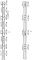
図1は、本発明に係るフラッシュメモリシステム1を概略的に示すブロック図である。
Hereinafter, embodiments of the present invention will be described in detail with reference to the drawings.
[Description of flash memory system 1]
FIG. 1 is a block diagram schematically showing a flash memory system 1 according to the present invention.
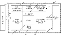
図1に示したようにフラッシュメモリシステム1は、フラッシュメモリ2と、それを制御するメモリコントローラ(以下、単にコントローラという)3とで構成されている。
フラッシュメモリシステム1は、通常、ホストシステム4に着脱可能に装着されて使用され、ホストシステム4に対して一種の外部記憶装置として用いられる。
尚、ホストシステム4としては、文字、音声、あるいは画像情報等の種々の情報を処理するパーソナルコンピュータやデジタルスチルカメラをはじめとする各種情報処理装置が挙げられる。
As shown in FIG. 1, the flash memory system 1 includes a
The flash memory system 1 is normally used by being detachably attached to the host system 4 and used as a kind of external storage device for the host system 4.
Examples of the host system 4 include various information processing apparatuses such as a personal computer and a digital still camera that process various information such as characters, sounds, and image information.
フラッシュメモリ2は、ページ単位で読出し又は書込みを行い、ブロック単位で消去を実行するデバイスである。例えば、1ブロックは32ページで構成され、1ページは512バイトのユーザ領域と16バイトの冗長領域で構成されている。
The
コントローラ3は、ホストインターフェース制御ブロック5と、マイクロプロセッサ6と、ホストインターフェースブロック7と、ワークエリア8と、バッファ9と、フラッシュメモリインターフェースブロック10と、ECC(エラー・コレクション・コード)ブロック11と、フラッシュメモリシーケンサブロック12とから構成されている。
The
これら機能ブロックによって構成されるコントローラ3は、一つの半導体チップ上に集積されている。以下に各ブロックの機能を説明する。
マイクロプロセッサ6は、コントローラ3を構成する各機能ブロック全体の動作を制御する機能ブロックである。
The
The
ホストインターフェース制御ブロック5は、ホストインターフェースブロック7の動作を制御する機能ブロックである。ここで、ホストインターフェース制御ブロック5は、ホストインターフェースブロック7の動作を設定する動作設定レジスタ(図示せず)を備えており、この動作設定レジスタに基づきホストインターフェースブロック7は動作する。 The host interface control block 5 is a functional block that controls the operation of the host interface block 7. Here, the host interface control block 5 includes an operation setting register (not shown) for setting the operation of the host interface block 7, and the host interface block 7 operates based on the operation setting register.
ホストインターフェースブロック7は、ホストシステム4とデータ、アドレス情報、ステータス情報及び外部コマンド情報の授受を行なう機能ブロックである。すなわち、フラッシュメモリシステム1がホストシステム4に装着されると、フラッシュメモリシステム1とホストシステム4は、外部バス13を介して相互に接続され、かかる状態において、ホストシステム4よりフラッシュメモリシステム1に供給されるデータ等は、ホストインターフェースブロック7を入口としてコントローラ3の内部に取り込まれる。フラッシュメモリシステム1からホストシステム4に供給されるデータ等は、ホストインターフェースブロック7を出口としてホストシステム4に供給される。
The host interface block 7 is a functional block that exchanges data, address information, status information, and external command information with the host system 4. That is, when the flash memory system 1 is attached to the host system 4, the flash memory system 1 and the host system 4 are connected to each other via the
さらに、ホストインターフェースブロック7は、ホストシステム4より供給されるホストアドレス及び外部コマンドを一時的に格納するタスクファイルレジスタ(図示せず)及びエラーが発生した場合にセットされるエラーレジスタ(図示せず)等を有している。 Further, the host interface block 7 includes a task file register (not shown) for temporarily storing a host address and an external command supplied from the host system 4 and an error register (not shown) set when an error occurs. ) Etc.
ワークエリア8は、フラッシュメモリ2の制御に必要なデータが一時的に格納される作業領域であり、複数のSRAM(Static Random Access Memory)セルによって構成される機能ブロックである。
The work area 8 is a work area in which data necessary for controlling the
バッファ9は、フラッシュメモリ2から読出したデータ及びフラッシュメモリ2に書込むデータを一時的に保持する機能ブロックである。すなわち、フラッシュメモリ2から読出したデータは、ホストシステム4の受取準備ができるまでバッファ9に保持される。フラッシュメモリ2に書込むデータは、フラッシュメモリ2の書込準備ができるまでバッファ9に保持される。
The
フラッシュメモリシーケンサブロック12は、内部コマンドに基づきフラッシュメモリ2の動作を制御する機能ブロックである。フラッシュメモリシーケンサブロック12は、複数のレジスタ(図示せず)を備え、この複数のレジスタに内部コマンドを実行する際に必要な情報が設定される。この複数のレジスタに内部コマンドを実行する際に必要な情報が設定されると、フラッシュメモリシーケンサブロック12は、その情報に基づいて処理を実行する。ここで、「内部コマンド」とは、コントローラ3からフラッシュメモリ2に与えられるコマンドであり、ホストシステム4からフラッシュメモリシステム1に与えられるコマンドの「外部コマンド」とは、区別される。
The flash
フラッシュメモリインターフェースブロック10は、内部バス14を介して、フラッシュメモリ2とデータ、アドレス情報、ステータス情報、内部コマンド情報及びデバイスID情報等の授受を行う機能ブロックである。
The flash
ECCブロック11は、フラッシュメモリ2に書込むデ―タに付加されるエラーコレクションコードを生成するとともに、読出しデータに付加されたエラーコレクションコードに基づいて、読出したデータに含まれる誤りを検出・訂正する機能ブロックである。
The
[フラッシュメモリ2の説明]
図1のフラッシュメモリ2は、NAND型メモリである。NAND型フラッシュメモリは、ストレージデバイスへの用途として(ハードディスクの代わりになるものとして)開発された不揮発性メモリである。このNAND型フラッシュメモリは、ランダムアクセスを行なうことができず、書込みと読出しはページ単位で、消去はブロック単位で行なわれる。データの上書きができないので、データを書込むときは、消去されている領域にデータの書込みが行なわれる。
[Description of flash memory 2]
The
フラッシュメモリ2は、このような特徴を有するため、通常、データの書替を行なう場合には、ブロック消去されている消去済ブロックに新たなデータ(書替後のデータ)を書込み、古いデータ(書替前のデータ)が書込まれていたブロックを消去するという処理を行なっている。このようなデータの書替を行なった場合、書替後のデータは書替前と異なるブロックに書込まれるため、ホストシステム4側から与えられるアドレスに基づく論理ブロックアドレスと、フラッシュメモリ2内でのブロックアドレスである物理ブロックアドレスとの対応関係は、データを書替える毎に動的に変化する。この論理ブロックアドレスと物理ブロックアドレスとの対応関係は、通常、その対応関係を示したアドレス変換テーブルによって管理されており、アドレス変換テーブルは、後述する対応論理ブロックアドレスに基づいて作成される。
Since the
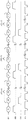
ここで、上記ブロックとページの関係を説明する。
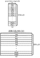
図2(a),(b)は、ブロックとページの関係を示す説明図てある。
ブロック及びページの構成は、フラッシュメモリ2の仕様によって異なるが、一般的なフラッシュメモリでは、図2(a)に示したように、1ブロックが32ページ(P0〜P31)で構成される。各ページが512バイトのユーザ領域と16バイトの冗長領域で構成されている。又、記憶容量の増加に伴い、図2(b)に示したように、1ブロックが64ページ(P0〜P63)で構成され、各ページが2048バイトのユーザ領域と64バイトの冗長領域で構成されているものも提供されている。
Here, the relationship between the block and the page will be described.
2A and 2B are explanatory diagrams showing the relationship between blocks and pages.
The configuration of blocks and pages varies depending on the specifications of the
ユーザ領域は、主に、ホストシステム4から供給されるデ―タが記憶される領域であり、冗長領域は、エラーコレクションコード、対応論理ブロックアドレス及びブロックステータス等の付加データが記憶される領域である。 The user area is mainly an area for storing data supplied from the host system 4, and the redundant area is an area for storing additional data such as an error correction code, a corresponding logical block address and a block status. is there.
エラ―コレクションコードは、ユーザ領域に記憶されているデータに含まれる誤りを検出、訂正するための付加データであり、外部のECCブロックによって生成される。対応論理ブロックアドレスは、そのブロックにデータが格納されている場合に、そのブロックがどの論理ブロックアドレスに対応するかを示している。 The error correction code is additional data for detecting and correcting an error included in data stored in the user area, and is generated by an external ECC block. The corresponding logical block address indicates to which logical block address the block corresponds when data is stored in the block.
尚、そのブロックにデータが格納されていない場合は、対応論理ブロックアドレスも格納されていないので、対応論理ブロックアドレスが格納されているか否かで、そのブロックが消去済ブロックであるか否かを判断することもできる。つまり、対応論理ブロックアドレスが格納されていない場合は、消去済ブロックであると判断される。 If no data is stored in the block, the corresponding logical block address is not stored. Therefore, whether or not the block is an erased block depends on whether or not the corresponding logical block address is stored. It can also be judged. That is, if the corresponding logical block address is not stored, it is determined that the block is an erased block.
ブロックステータスは、そのブロックが不良ブロック(正常にデータの書込み等を行なうことができないブロック)であるか否かを示すフラグであり、そのブロックが不良ブロックであると判断された場合には、不良ブロックであることを示すフラグが設定される。 The block status is a flag indicating whether or not the block is a bad block (a block in which data cannot be normally written). If it is determined that the block is a bad block, the block status is bad. A flag indicating a block is set.
次に、フラッシュメモリ2の回路構成について説明する。
フラッシュメモリ2は、一般的なNAND型フラッシュメモリと同様に、メモリ書込みデータ若しくは読出しデータを保持するためのレジスタと、データを記憶するメモリセルアレイによって構成されている。メモリセルアレイは、複数のメモリセルが直列に接続されたメモリセル群を複数備えており、ワード線によってメモリセル群の特定のメモリセルが選択される。このワード線によって選択されたメモリセルとレジスタの間で、データの複写(レジスタからメモリセルへの複写、若しくはメモリセルからレジスタへの複写)が行なわれる。
Next, the circuit configuration of the
The
メモリセルアレイを構成するメモリセルは、2つのゲートを備えたMOSトランジスタで構成されている。ここで、上側のゲートはコントロールゲートと、下側のゲートはフローティングゲートと呼ばれており、フローティングゲートに電荷(電子)を注入若しくはフローティングゲートから電荷(電子)を排出することによって、データの書込み若しくはデータの消去を行なっている。このフローティングゲートは周囲を絶縁体で囲まれているので、注入された電子は長期間にわたって保持される。 A memory cell constituting the memory cell array is composed of a MOS transistor having two gates. Here, the upper gate is called a control gate and the lower gate is called a floating gate. Data is written by injecting charges (electrons) into the floating gate or discharging charges (electrons) from the floating gate. Or data is erased. Since the floating gate is surrounded by an insulator, the injected electrons are held for a long period of time.
尚、フローティングゲートに電子を注入するときは、コントロールゲートが高電位側となる高電圧を印加して電子を注入し、フローティングゲートから電子を排出するときは、コントロールゲートが低電位側となる高電圧を印加して電子を排出する。ここで、フローティングゲートに電子が注入されている状態(書込状態)が、論理値の「0」のデータに対応し、フローティングゲートから電子が排出されている状態(消去状態)が、論理値の「1」のデータに対応する。
[動作の説明]
次に、ホストシステムから供給されるユーザデータが、フラッシュメモリ2に書込まれる過程を、図3を参照して説明する。
図3は、フラッシュメモリシステムの動作の説明図である。
When electrons are injected into the floating gate, a high voltage is applied so that the control gate is on the high potential side. When electrons are injected, and when electrons are discharged from the floating gate, the control gate is on the low potential side. A voltage is applied to discharge electrons. Here, the state in which electrons are injected into the floating gate (write state) corresponds to the data of logical value “0”, and the state in which electrons are discharged from the floating gate (erased state) is the logical value. Corresponds to the data of “1”.
[Description of operation]
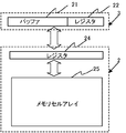
Next, a process in which user data supplied from the host system is written to the
FIG. 3 is an explanatory diagram of the operation of the flash memory system.
図3のバッファ21と付加データ用レジスタ22は、図1のコントローラ3内に構成されており、バッファ21にはホストシステム4から供給されるユーザデータが保持され、付加データ用レジスタ22にはエラーコレクションコード等の付加データが設定されている。
The
一方、レジスタ24とメモリセルアレイ25は、フラッシュメモリ2内に構成されており、レジスタ24はコントローラ3から供給されるデータ又はメモリセルアレイ25から出力されたデータを保持し、メモリセルアレイ25はコントローラ3から供給されるデータを記憶する。ここで、レジスタ24の容量は、フラッシュメモリ2のページの容量と同一になっている。
On the other hand, the
ホストシステム4から供給されるユーザデータをフラッシュメモリ2に書込むときは、ホストシステム4から供給されるユーザデータがバッファ21に保持され、バッファ21に保持されたユーザデータに対して作成されたエラーコレクションコードやその他の付加データが、付加データ用レジスタ22に設定される。バッファ21に保持されたユーザデータと付加データ用レジスタ22に設定された付加データは、フラッシュメモリ2に転送され、フラッシュメモリ2内のレジスタ24に保持される。レジスタ24に保持されたユーザデータと付加データは、コントローラ3から指定されたページに複写(記憶)される。
When writing user data supplied from the host system 4 to the
従来のフラッシュメモリでは、図4に示したように、ページ内の先頭側の領域にユーザ領域が割当てられ、ページ内の末尾側の領域に冗長領域が割当てられていた。
図4(a),(b)は、従来の書込み状況を示す模式図である。
図4(a)に示した例では、先頭側の512バイトがユーザ領域に割当てられ、末尾側の16バイトが冗長領域に割当てられている。図4(b)に示した例では、先頭側の2048バイトがユーザ領域に割当てられ、末尾側の64バイトが冗長領域に割当てられている。このように、ユーザ領域はページ内の先頭側に、冗長領域はページ内の末尾側に、それぞれ固めて割当てられていた。
In the conventional flash memory, as shown in FIG. 4, the user area is assigned to the top area in the page, and the redundant area is assigned to the end area in the page.
4 (a) and 4 (b) are schematic diagrams showing a conventional writing situation.
In the example shown in FIG. 4A, the first 512 bytes are allocated to the user area, and the last 16 bytes are allocated to the redundant area. In the example shown in FIG. 4B, the first 2048 bytes are allocated to the user area, and the last 64 bytes are allocated to the redundant area. As described above, the user area is assigned to the head side of the page and the redundant area is assigned to the end side of the page.
尚、フラッシュメモリ2への書込処理では、フラッシュメモリ2内のレジスタに保持されたデータが、フラッシュメモリ2内のページに複写されるので、フラッシュメモリ2内のレジスタにユーザデータと付加データとを転送するときには、ページ内のユーザ領域と冗長領域の割当てに従って、データの転送を行なわなければならない。つまり、ページ内の先頭側の領域にユーザ領域が割当てられ、ページ内の末尾側の領域に冗長領域が割当てられている場合は、レジスタ内の先頭側の領域にユーザデータ(ユーザ領域に書込まれるデータ)が保持され、末尾側の領域に付加データ(冗長領域に書込まれるデータ)が保持されるようにデータの転送を行なわなければならない。
In the writing process to the
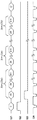
次に、コントローラ内の512バイトのバッファと16バイトの付加データ用レジスタを用いて、ユーザ領域が2048バイトのページ(図4(b))にデータを書込む場合の処理について、図面を参照して説明する。
図5は、従来の書込処理でフラッシュメモリ2内のレジスタに保持されたデータを示す図である。図6は、本発明に係る書込処理でフラッシュメモリ2内のレジスタに保持されたデータを示すである。
Next, refer to the drawing for processing when data is written to a page with a user area of 2048 bytes (FIG. 4B) using a 512-byte buffer and a 16-byte additional data register in the controller. I will explain.
FIG. 5 is a diagram showing data held in a register in the
尚、書込処理では、上述のようにフラッシュメモリ内のレジスタに保持されたデータが、書込先のページに複写されるので、レジスタに保持されるユーザデータと付加データの配列と、書込先のページに複写されるデータのユーザデータと付加データの配列は同一になる。よって、フラッシュメモリ内のレジスタで、ユーザデータが保持される領域が、ページ内のユーザ領域に対応し、付加データが保持される領域が、ページ内の冗長領域に対応する。このため、以下の説明では、フラッシュメモリ内のレジスタに保持されるユーザデータと付加データの配列を中心に説明する。 In the writing process, as described above, the data held in the register in the flash memory is copied to the page of the write destination, so that the arrangement of user data and additional data held in the register, the write The arrangement of user data and additional data of data copied to the previous page is the same. Therefore, in the register in the flash memory, an area in which user data is held corresponds to a user area in a page, and an area in which additional data is held corresponds to a redundant area in the page. For this reason, the following description will focus on the arrangement of user data and additional data held in a register in the flash memory.
図5に示した従来の書込処理では、フラッシュメモリに対して、次のような順序でユーザデータと付加データが転送される。ステップ0でユーザデータが転送され、ステップ1で付加データが転送され、ステップ2でユーザデータが転送され、ステップ3で付加データが転送され、ステップ4でユーザデータが転送され、ステップ5で付加データが転送され、ステップ6でユーザデータが転送され、ステップ7で付加データが転送される。
In the conventional writing process shown in FIG. 5, user data and additional data are transferred to the flash memory in the following order. User data is transferred at step 0, additional data is transferred at step 1, user data is transferred at
ここで、ステップ1で転送される付加データはステップ0で転送されるユーザデータに対応し、ステップ3で転送される付加データはステップ2で転送されるユーザデータに対応し、ステップ5で転送される付加データはステップ4で転送されるユーザデータに対応し、ステップ7で転送される付加データはステップ6で転送されるユーザデータに対応する。又、ステップ0、ステップ2、ステップ4及びステップ6で転送されるユーザデータは、レジスタの先頭側の領域からこの順番で保持され、ステップ1、ステップ3、ステップ5及びステップ7で転送される付加データは、ユーザデータの後にこの順番で保持される。
Here, the additional data transferred in step 1 corresponds to the user data transferred in step 0, and the additional data transferred in
図6(a)に示した本発明に係る書込処理では、フラッシュメモリに対して、次のような順番でユーザデータと付加データが転送され、転送された順番でフラッシュメモリ内のレジスタに保持される。ステップA0でユーザデータが転送され、ステップA1で付加データが転送され、ステップA2でユーザデータが転送され、ステップA3で付加データが転送され、ステップA4でユーザデータが転送され、ステップA5で付加データが転送され、ステップA6でユーザデータが転送され、ステップA7で付加データが転送される。ここで、ステップA1で転送される付加データはステップA0で転送されるユーザデータに対応し、ステップA3で転送される付加データはステップA2で転送されるユーザデータに対応し、ステップA5で転送される付加データはステップA4で転送されるユーザデータに対応し、ステップA7で転送される付加データはステップA6で転送されるユーザデータに対応する。 In the write processing according to the present invention shown in FIG. 6A, user data and additional data are transferred to the flash memory in the following order, and are held in the registers in the flash memory in the transferred order. Is done. User data is transferred at step A0, additional data is transferred at step A1, user data is transferred at step A2, additional data is transferred at step A3, user data is transferred at step A4, and additional data at step A5. Is transferred, user data is transferred in step A6, and additional data is transferred in step A7. Here, the additional data transferred in step A1 corresponds to the user data transferred in step A0, the additional data transferred in step A3 corresponds to the user data transferred in step A2, and transferred in step A5. The additional data to be transferred corresponds to the user data transferred in step A4, and the additional data transferred in step A7 corresponds to the user data transferred in step A6.
つまり、本発明に係る書込処理では、512バイトのユーザデータとこれに対応する16バイトの付加データがレジスタ内の連続した領域に保持される。又、ユーザデータと付加データとは、レジスタ内の領域に交互に配列される。これに対応して、レジスタに保持されていたデータが複写されるページ内の領域も、512バイトのユーザ領域と16バイトの冗長領域が交互に割当てられる。 That is, in the writing process according to the present invention, 512 bytes of user data and 16 bytes of additional data corresponding to the user data are held in a continuous area in the register. Further, the user data and the additional data are alternately arranged in the area in the register. Correspondingly, a 512-byte user area and a 16-byte redundant area are alternately assigned to areas in the page where the data held in the register is copied.
図6(a)に示した例では、512バイトのバッファと16バイトの付加データ用レジスタを用いて書込処理を行なったが、図6(b)に示した例では、1024バイトのバッファと32バイトの付加データ用レジスタを用いて書込処理を行なっている。1024バイトのバッファと32バイトの付加データ用レジスタを用いて書込処理を行なった場合も、ユーザデータとこれに対応する付加データがレジスタ内の連続した領域に保持される。又、ユーザデータと付加データは、レジスタ内の領域に交互に配列される。但し、1024バイトのバッファと32バイトの付加データ用レジスタを用いて書込処理を行なっているので、ページ内の領域には、1024バイトのユーザ領域と32バイトの冗長領域が交互に割当てられる。 In the example shown in FIG. 6A, the writing process is performed using a 512-byte buffer and a 16-byte additional data register. In the example shown in FIG. Write processing is performed using a 32-byte additional data register. Even when a write process is performed using a 1024-byte buffer and a 32-byte additional data register, user data and additional data corresponding to the user data are held in a continuous area in the register. User data and additional data are alternately arranged in areas in the register. However, since writing processing is performed using a 1024-byte buffer and a 32-byte additional data register, a 1024-byte user area and a 32-byte redundant area are alternately allocated to the area in the page.
次に、図5に示した従来の書込処理でフラッシュメモリに供給される信号と、図6(a)に示した本発明に係る書込処理でフラッシュメモリに供給される信号について図面を参照して説明する。
図7は、従来の書込処理でフラッシュメモリ2に供給される信号の波形図であり、図8は、図6(a)に示した本発明に係る書込処理でフラッシュメモリ2に供給される信号の波形図である。
図7に示した波形図で、S11は、コマンド、アドレス及びデータ(ユーザデータ、付加データ等)等を供給するデータバスに出力されるデータ信号である。S12は、データバスに出力されている信号がコマンドを示す信号であるときに高レベルとなるコマンドラッチイネーブル信号である。S13は、データバスに出力されている信号がアドレスを示す信号であるときに高レベルとなるアドレスラッチイネーブル信号である。S14は、データバスにコマンド、アドレス及びデータが出力されているときに低レベルから高レベルに変化するライトイネーブル信号である。尚、コマンドラッチイネーブル信号、アドレスラッチイネーブル信号及びライトイネーブル信号以外の制御信号については図示していない。又、以下の説明で、データバスに出力されるコマンドを示す信号をコマンド信号と言い、アドレスを示す信号をアドレス信号と言い、ユーザデータを示す信号をユーザデータ信号と言い、付加データを示す信号を付加データ信号と言う。
Next, refer to the drawings for the signals supplied to the flash memory in the conventional writing process shown in FIG. 5 and the signals supplied to the flash memory in the writing process according to the present invention shown in FIG. To explain.
FIG. 7 is a waveform diagram of signals supplied to the
In the waveform diagram shown in FIG. 7, S11 is a data signal output to a data bus for supplying commands, addresses, data (user data, additional data, etc.) and the like. S12 is a command latch enable signal that goes high when the signal output to the data bus is a signal indicating a command. S13 is an address latch enable signal that goes high when the signal output to the data bus is a signal indicating an address. S14 is a write enable signal that changes from a low level to a high level when a command, an address, and data are output to the data bus. Control signals other than the command latch enable signal, address latch enable signal, and write enable signal are not shown. In the following description, a signal indicating a command output to the data bus is referred to as a command signal, a signal indicating an address is referred to as an address signal, a signal indicating user data is referred to as a user data signal, and a signal indicating additional data. Is called an additional data signal.
図7に示した従来の書込処理における波形図では、まず、データバスに書込コマンドに対応するコマンド信号Cが出力され、続いて、ステップ0に対応するアドレス信号A0、ユーザデータ信号D0〜D511及びアドレス変更コマンドに対応するコマンドC”が順次出力され、その後、ステップ1に対応するアドレス信号A1及び付加データ信号D0’〜D15’が順次出力される。以下同様に、ステップ2、ステップ4及びステップ6に対応するアドレス信号、ユーザデータ信号及びアドレス変更コマンドに対応するコマンドC”が順次出力され、その後にステップ3、ステップ5及びステップ7に対応するアドレス信号及び付加データ信号が順次出力される。以上の処理で、フラッシュメモリ内のレジスタに保持されたデータは、データ複写に対応するコマンド信号C’によって、レジスタから書込み先ページに複写される。尚、データバスに出力された信号は、ライトイネーブル信号(S14)の立上りでフラッシュメモリに取込まれ、コマンドラッチイネーブル信号(S12)が高レベルのときに取込まれた信号はコマンド信号と判断され、アドレスラッチイネーブル信号(S13)が高レベルのときに取込まれた信号はアドレス信号と判断される。
In the waveform diagram in the conventional writing process shown in FIG. 7, first, a command signal C corresponding to a write command is output to the data bus, and subsequently, an address signal A0 corresponding to step 0, and user data signals D0 to D0. D511 and the command C ″ corresponding to the address change command are sequentially output, and thereafter, the address signal A1 and the additional data signals D0 ′ to D15 ′ corresponding to step 1 are sequentially output. In addition, an address signal corresponding to Step 6 and a command C ″ corresponding to a user data signal and an address change command are sequentially output, and then an address signal and an additional data signal corresponding to
図7に示した従来の書込処理における波形図では、各ステップの最初にアドレス変更コマンドに対応するコマンドC”とアドレス信号が出力されている。これは、各ステップの変り目でアドレスが不連続になるため、書込先のアドレスを指定しているからである。尚、指定されたアドレスは、ライトイネーブル信号の立上りでカウントアップされるので、アドレス信号で書込先のアドレスを指定しなかった場合、ユーザデータ信号若しくは付加データ信号に対応するデータは連続したアドレスに順次取込まれる。 In the waveform diagram in the conventional writing process shown in FIG. 7, the command C ″ corresponding to the address change command and the address signal are output at the beginning of each step. This is because the address is discontinuous at the transition of each step. This is because the address of the write destination is designated because the designated address is counted up at the rising edge of the write enable signal, and the address of the write destination is not designated by the address signal. In this case, data corresponding to the user data signal or the additional data signal is sequentially taken in consecutive addresses.
図8に示した波形図で、S21は、コマンド、アドレス及びデータ(ユーザデータ、付加データ等)等を供給するデータバスに出力されるデータ信号である。S22は、データバスに出力されている信号がコマンドを示す信号であるときに高レベルとなるコマンドラッチイネーブル信号である。、S23は、データバスに出力されている信号がアドレスを示す信号であるときに高レベルとなるアドレスラッチイネーブル信号である。S24は、データバスにコマンド、アドレス及びデータが出力されているときに低レベルから高レベルに変化するライトイネーブル信号である。 In the waveform diagram shown in FIG. 8, S21 is a data signal output to a data bus for supplying commands, addresses, data (user data, additional data, etc.) and the like. S22 is a command latch enable signal that goes high when the signal output to the data bus is a signal indicating a command. , S23 is an address latch enable signal that goes high when the signal output to the data bus is a signal indicating an address. S24 is a write enable signal that changes from a low level to a high level when a command, an address, and data are output to the data bus.
図8に示した本発明に係る書込処理における波形図では、まず、データバスに書込コマンドに対応するコマンド信号Cが出力され、続いて、ステップA0に対応するアドレス信号A0及びユーザデータ信号D0〜D511が順次出力され、更に、ステップA1に対応する付加データ信号D0’〜D15’が順次出力される。以下同様に、ステップA2、ステップA4及びステップA6に対応するユーザデータ信号と、ステップA3、ステップA5及びステップA7に対応する付加データ信号が、ステップA2、ステップA3、…、ステップA7の順で出力される。以上の処理で、フラッシュメモリ内のレジスタに保持されたデータは、データ複写に対応するコマンド信号C’によって、レジスタから書込み先ページに複写される。 In the waveform diagram in the writing process according to the present invention shown in FIG. 8, first, the command signal C corresponding to the write command is output to the data bus, and then the address signal A0 and the user data signal corresponding to step A0. D0 to D511 are sequentially output, and additional data signals D0 ′ to D15 ′ corresponding to step A1 are sequentially output. Similarly, user data signals corresponding to step A2, step A4 and step A6 and additional data signals corresponding to step A3, step A5 and step A7 are output in the order of step A2, step A3,..., Step A7. Is done. With the above processing, the data held in the register in the flash memory is copied from the register to the write destination page by the command signal C ′ corresponding to data copying.
尚、データバスに出力された信号は、ライトイネーブル信号(S24)の立上りでフラッシュメモリに取込まれ、コマンドラッチイネーブル信号(S22)が高レベルのときに取込まれた信号はコマンド信号と判断され、アドレスラッチイネーブル信号(S23)が高レベルのときに取込まれた信号はアドレス信号と判断される。 The signal output to the data bus is taken into the flash memory at the rising edge of the write enable signal (S24), and the signal taken when the command latch enable signal (S22) is at the high level is determined as the command signal. The signal taken in when the address latch enable signal (S23) is at the high level is determined as the address signal.
図8に示した本発明に係る書込処理における波形図では、ステップ0の最初にアドレス信号が出力され、それ以降のステップ1〜7では、アドレス変更コマンドに対応するコマンド信号やアドレス信号が出力されない。これは、ステップ0〜7で出力されるユーザデータ信号若しくは付加データ信号に対応するデータが、ずっと連続したアドレスに順次取込まれるからである。 In the waveform diagram in the writing process according to the present invention shown in FIG. 8, an address signal is output at the beginning of Step 0, and a command signal and an address signal corresponding to the address change command are output in Steps 1 to 7 thereafter. Not. This is because the data corresponding to the user data signal or the additional data signal output in steps 0 to 7 is sequentially taken into continuous addresses.
以上のように、本実施形態のフラッシュメモリシステム1では、ユーザデータと付加データを転送する場合に、転送データがユーザデータから付加データに変る場合、又は付加データからユーザデータに変る場合に書込先のアドレスを変更する必要がない。したがって、書込処理の処理効率を向上させることができる。 As described above, in the flash memory system 1 of the present embodiment, when user data and additional data are transferred, writing is performed when the transfer data changes from user data to additional data, or when the additional data changes from user data to user data. There is no need to change the destination address. Therefore, the processing efficiency of the writing process can be improved.
1 フラッシュメモリシステム
2 フラッシュメモリ
3 メモリコントローラ
4 ホストシステム
1
Claims (7)
前記ユーザデータに対応する付加データを保持する第2のデータ保持機能と、
前記第1のデータ保持機能に保持されているユーザデータと前記第2のデータ保持機能に保持されている付加データとをフラッシュメモリに転送するデータ転送機能とを備え、
前記フラッシュメモリ内のページに、前記ユーザデータと該ユーザデータに対応する前記付加データとを複数組書込み、且つ、該ユーザデータと該ユーザデータに対応する該付加データとを連続した位置に書込む構成にされていることを特徴とするメモリコントローラ。 A first data holding function for holding user data supplied from the host system side;
A second data holding function for holding additional data corresponding to the user data;
A data transfer function for transferring user data held in the first data holding function and additional data held in the second data holding function to a flash memory;
A plurality of sets of the user data and the additional data corresponding to the user data are written to a page in the flash memory, and the user data and the additional data corresponding to the user data are written in consecutive positions. A memory controller characterized by being configured.
前記第1のデータ保持機能の容量が512バイトであり、
前記第2のデータ保持機能の容量が16バイトである、
ことを特徴とする請求項1又は2記載のメモリコントローラ。 The page has a capacity of 2112 bytes;
The capacity of the first data holding function is 512 bytes;
The capacity of the second data holding function is 16 bytes;
3. The memory controller according to claim 1, wherein the memory controller is a memory controller.
前記フラッシュメモリ内のページに、前記ユーザデータと該ユーザデータに対応する前記付加データとを複数組書込み、且つ、該ユーザデータと該ユーザデータに対応する該付加データを連続して書込むことを特徴とするフラッシュメモリの制御方法。 Processing for transferring user data supplied from the host system side held in the first data holding function to the flash memory, and flashing additional data corresponding to the user data held in the second data holding function By repeating the process of transferring to the memory several times alternately,
Writing a plurality of sets of the user data and the additional data corresponding to the user data to the page in the flash memory, and continuously writing the user data and the additional data corresponding to the user data A flash memory control method.
7. The capacity of the page is 2112 bytes, the capacity of the first data holding function is 512 bytes, and the capacity of the second data holding function is 16 bytes. Flash memory control method.
Priority Applications (1)
| Application Number | Priority Date | Filing Date | Title |
|---|---|---|---|
| JP2004103307A JP2005292925A (en) | 2004-03-31 | 2004-03-31 | Memory controller, flash memory system, and control method for flash memory |
Applications Claiming Priority (1)
| Application Number | Priority Date | Filing Date | Title |
|---|---|---|---|
| JP2004103307A JP2005292925A (en) | 2004-03-31 | 2004-03-31 | Memory controller, flash memory system, and control method for flash memory |
Publications (1)
| Publication Number | Publication Date |
|---|---|
| JP2005292925A true JP2005292925A (en) | 2005-10-20 |
Family
ID=35325827
Family Applications (1)
| Application Number | Title | Priority Date | Filing Date |
|---|---|---|---|
| JP2004103307A Pending JP2005292925A (en) | 2004-03-31 | 2004-03-31 | Memory controller, flash memory system, and control method for flash memory |
Country Status (1)
| Country | Link |
|---|---|
| JP (1) | JP2005292925A (en) |
Cited By (6)
| Publication number | Priority date | Publication date | Assignee | Title |
|---|---|---|---|---|
| JP2008112335A (en) * | 2006-10-31 | 2008-05-15 | Tdk Corp | Memory controller and flash memory system equipped with memory controller and method for controlling flash memory |
| JP2013016148A (en) * | 2011-06-08 | 2013-01-24 | Panasonic Corp | Memory controller and nonvolatile storage |
| JP2013050938A (en) * | 2011-08-01 | 2013-03-14 | Toshiba Corp | Memory device |
| US8656252B2 (en) | 2011-06-08 | 2014-02-18 | Panasonic Corporation | Memory controller and non-volatile storage device |
| US8856427B2 (en) | 2011-06-08 | 2014-10-07 | Panasonic Corporation | Memory controller and non-volatile storage device |
| JPWO2017183153A1 (en) * | 2016-04-21 | 2018-07-19 | 富士通フロンテック株式会社 | WRITE CONTROL PROGRAM, WRITE CONTROL DEVICE, AND WRITE CONTROL METHOD |
-
2004
- 2004-03-31 JP JP2004103307A patent/JP2005292925A/en active Pending
Cited By (8)
| Publication number | Priority date | Publication date | Assignee | Title |
|---|---|---|---|---|
| JP2008112335A (en) * | 2006-10-31 | 2008-05-15 | Tdk Corp | Memory controller and flash memory system equipped with memory controller and method for controlling flash memory |
| JP4569554B2 (en) * | 2006-10-31 | 2010-10-27 | Tdk株式会社 | MEMORY CONTROLLER, FLASH MEMORY SYSTEM HAVING MEMORY CONTROLLER, AND FLASH MEMORY CONTROL METHOD |
| JP2013016148A (en) * | 2011-06-08 | 2013-01-24 | Panasonic Corp | Memory controller and nonvolatile storage |
| US8656252B2 (en) | 2011-06-08 | 2014-02-18 | Panasonic Corporation | Memory controller and non-volatile storage device |
| US8856427B2 (en) | 2011-06-08 | 2014-10-07 | Panasonic Corporation | Memory controller and non-volatile storage device |
| US8898420B2 (en) | 2011-06-08 | 2014-11-25 | Panasonic Corporation | Non-volatile storage device and a memory controller controlling parity tables of recording regions of the non-volatile storage device |
| JP2013050938A (en) * | 2011-08-01 | 2013-03-14 | Toshiba Corp | Memory device |
| JPWO2017183153A1 (en) * | 2016-04-21 | 2018-07-19 | 富士通フロンテック株式会社 | WRITE CONTROL PROGRAM, WRITE CONTROL DEVICE, AND WRITE CONTROL METHOD |
Similar Documents
| Publication | Publication Date | Title |
|---|---|---|
| JP4373943B2 (en) | Memory controller, flash memory system, and flash memory control method | |
| JP2004507007A (en) | Novel method and structure for performing a reliable data copy process on non-volatile memory | |
| US9383929B2 (en) | Data storing method and memory controller and memory storage device using the same | |
| JP2006018373A (en) | Memory controller, flash memory system and control method for flash memory | |
| JP4661497B2 (en) | Memory controller, flash memory system, and flash memory control method | |
| JP4661369B2 (en) | Memory controller | |
| JP4661191B2 (en) | Memory controller, flash memory system, and flash memory control method | |
| JP2005292925A (en) | Memory controller, flash memory system, and control method for flash memory | |
| JP4609406B2 (en) | MEMORY CONTROLLER, FLASH MEMORY SYSTEM PROVIDED WITH MEMORY CONTROLLER, AND FLASH MEMORY CONTROL METHOD | |
| JP4177292B2 (en) | MEMORY CONTROLLER, FLASH MEMORY SYSTEM, AND FLASH MEMORY CONTROL METHOD | |
| JP4655034B2 (en) | Memory controller, flash memory system, and flash memory control method | |
| JP4000124B2 (en) | MEMORY CONTROLLER, FLASH MEMORY SYSTEM PROVIDED WITH MEMORY CONTROLLER, AND FLASH MEMORY CONTROL METHOD | |
| JP4697146B2 (en) | MEMORY CONTROLLER, FLASH MEMORY SYSTEM HAVING MEMORY CONTROLLER, AND FLASH MEMORY CONTROL METHOD | |
| JP4661748B2 (en) | MEMORY CONTROLLER, FLASH MEMORY SYSTEM HAVING MEMORY CONTROLLER, AND FLASH MEMORY CONTROL METHOD | |
| JP4194518B2 (en) | Memory controller, flash memory system, and flash memory control method | |
| JP3934659B1 (en) | Memory controller and flash memory system | |
| JP4177301B2 (en) | Memory controller, flash memory system, and flash memory control method | |
| JP4304167B2 (en) | Memory controller, flash memory system, and flash memory control method | |
| JP4235595B2 (en) | MEMORY CONTROLLER, FLASH MEMORY SYSTEM PROVIDED WITH MEMORY CONTROLLER, AND FLASH MEMORY CONTROL METHOD | |
| JP4366283B2 (en) | Memory controller and flash memory system including the memory controller | |
| JP4332108B2 (en) | Memory controller, flash memory system, and flash memory control method | |
| JP4254930B2 (en) | Memory controller, flash memory system, and flash memory control method | |
| JP2005293177A (en) | Memory controller and flash memory system | |
| JP4561110B2 (en) | MEMORY CONTROLLER, FLASH MEMORY SYSTEM PROVIDED WITH MEMORY CONTROLLER, AND FLASH MEMORY CONTROL METHOD | |
| JP4282410B2 (en) | Flash memory control circuit, and memory controller and flash memory system provided with the control circuit |
Legal Events
| Date | Code | Title | Description |
|---|---|---|---|
| A977 | Report on retrieval |
Free format text: JAPANESE INTERMEDIATE CODE: A971007 Effective date: 20070221 |
|
| A131 | Notification of reasons for refusal |
Free format text: JAPANESE INTERMEDIATE CODE: A131 Effective date: 20070227 |
|
| A02 | Decision of refusal |
Effective date: 20070703 Free format text: JAPANESE INTERMEDIATE CODE: A02 |