JP2004362744A - Memory element - Google Patents
Memory element Download PDFInfo
- Publication number
- JP2004362744A JP2004362744A JP2004103091A JP2004103091A JP2004362744A JP 2004362744 A JP2004362744 A JP 2004362744A JP 2004103091 A JP2004103091 A JP 2004103091A JP 2004103091 A JP2004103091 A JP 2004103091A JP 2004362744 A JP2004362744 A JP 2004362744A
- Authority
- JP
- Japan
- Prior art keywords
- output
- input
- inverter
- signal
- data
- Prior art date
- Legal status (The legal status is an assumption and is not a legal conclusion. Google has not performed a legal analysis and makes no representation as to the accuracy of the status listed.)
- Pending
Links
Images


Classifications
-
- G—PHYSICS
- G11—INFORMATION STORAGE
- G11C—STATIC STORES
- G11C7/00—Arrangements for writing information into, or reading information out from, a digital store
- G11C7/10—Input/output [I/O] data interface arrangements, e.g. I/O data control circuits, I/O data buffers
-
- G—PHYSICS
- G11—INFORMATION STORAGE
- G11C—STATIC STORES
- G11C7/00—Arrangements for writing information into, or reading information out from, a digital store
- G11C7/10—Input/output [I/O] data interface arrangements, e.g. I/O data control circuits, I/O data buffers
- G11C7/1051—Data output circuits, e.g. read-out amplifiers, data output buffers, data output registers, data output level conversion circuits
- G11C7/1069—I/O lines read out arrangements
-
- G—PHYSICS
- G11—INFORMATION STORAGE
- G11C—STATIC STORES
- G11C7/00—Arrangements for writing information into, or reading information out from, a digital store
- G11C7/10—Input/output [I/O] data interface arrangements, e.g. I/O data control circuits, I/O data buffers
- G11C7/1006—Data managing, e.g. manipulating data before writing or reading out, data bus switches or control circuits therefor
- G11C7/1012—Data reordering during input/output, e.g. crossbars, layers of multiplexers, shifting or rotating
-
- G—PHYSICS
- G11—INFORMATION STORAGE
- G11C—STATIC STORES
- G11C7/00—Arrangements for writing information into, or reading information out from, a digital store
- G11C7/10—Input/output [I/O] data interface arrangements, e.g. I/O data control circuits, I/O data buffers
- G11C7/1051—Data output circuits, e.g. read-out amplifiers, data output buffers, data output registers, data output level conversion circuits
-
- G—PHYSICS
- G11—INFORMATION STORAGE
- G11C—STATIC STORES
- G11C7/00—Arrangements for writing information into, or reading information out from, a digital store
- G11C7/10—Input/output [I/O] data interface arrangements, e.g. I/O data control circuits, I/O data buffers
- G11C7/1078—Data input circuits, e.g. write amplifiers, data input buffers, data input registers, data input level conversion circuits
- G11C7/1096—Write circuits, e.g. I/O line write drivers
Abstract
Description
本発明は、半導体メモリ素子に関し、特に、読み出し/書き込み動作時に共有して使用されるグローバル入出力(Global Input Output: 以下、「GIO」と記す)ラインを、読み出し動作に用いられるMOBラインと書き込み動作に用いられるDINBラインとに各々分離し、また、入出力マルチプレクサの構造を変更することによって、リピータを使用する場合に発生するデータエラーを防止するメモリ素子に関する。 The present invention relates to a semiconductor memory device, in particular, a global input / output (Global Input Output: hereinafter, referred to as "GIO") line used in common during a read / write operation, and a MOB line used in a read operation. The present invention relates to a memory device which separates a DINB line used for an operation from each other and changes a structure of an input / output multiplexer to prevent a data error occurring when a repeater is used.
従来技術に係るメモリ素子において、グローバル入出力ラインは、読み出し/書き込み動作時に共通して用いられる。このような読み出し/書き込み動作時における概略的なデータの入出力経路を図1に示した。 In a memory device according to the related art, a global input / output line is commonly used during a read / write operation. FIG. 1 shows a schematic data input / output path during such a read / write operation.
図1を参照して、セルに格納されたデータを外部に読みだす読み出し動作に関して述べると、次のようである。まず、セルに格納されたデータはビットライン感知増幅器(BLSA)100を通して出力され、ビットライン感知増幅器100の出力はメイン増幅器(Main Amp)101を経てGIOラインに出力される。
Referring to FIG. 1, a read operation for reading data stored in a cell to the outside will be described as follows. First, data stored in a cell is output through a bit line sense amplifier (BLSA) 100, and an output of the bit
メモリにおいてGIOラインは非常に長いラインであり、時にはその長さが8000μmを超えることもある。したがって、このように負荷が大きいGIOラインを駆動するためにメイン増幅器101が用いられる。しかし、メイン増幅器101を使用してGIOラインに信号を印加しても、GIOラインに存在する大きい負荷のため信号速度が減少するので、これを補完する目的としてリピータ(repeater)をGIOラインに接続して使用する。図1にはリピータは図示されていない。リピータの構成については後述する。
GIO lines in memory are very long lines, sometimes having a length exceeding 8000 μm. Therefore, the
このようにメイン増幅器101を経てGIOラインに出力されたデータは入出力マルチプレクサ(I/O MUX)103に入力された後、入出力マルチプレクサ103から選択的に出力されてデータ出力バッファ(図示せず)へ出力される。ここで、入出力マルチプレクサ103は、X4、X8、X16モードなどデータ幅によるモード区別及び並列テストモードのために用いられる。
The data output to the GIO line via the
次いで、図1を参照して、セルにデータを格納する書き込み動作について述べる。セルに格納しようとする入力データDINはデータ入力ドライバー(図示せず)を通して入出力書き込み部(WT_IO)104に入力され、入出力書き込み部104は入力されたデータを増幅してGIOラインに出力する。GIOラインに出力された入力データは、書き込みドライバー(WT_DRV)102に入力された後、ビットライン感知増幅器100を経てセルに格納される。
Next, a write operation of storing data in a cell will be described with reference to FIG. Input data DIN to be stored in a cell is input to an input / output writing unit (WT_IO) 104 through a data input driver (not shown), and the input /
このように従来技術に係るメモリ素子では、読み出し動作及び書き込み動作時にGIOラインを共有して使用し、また、GIOラインの信号伝達速度を増大させるためにリピータを使用していた。このようなリピータを使用する場合、ノイズに敏感なリピータはGIOラインに出力されたデータを変化させるエラーを発生する場合がある。これに関しては、図2ないし図4を参照して説明する。 As described above, in the memory device according to the related art, the GIO line is shared and used during the read operation and the write operation, and the repeater is used to increase the signal transmission speed of the GIO line. When such a repeater is used, a repeater that is sensitive to noise may generate an error that changes data output to the GIO line. This will be described with reference to FIGS.
以下の説明において、Hは論理ハイ(logic high)を意味し、Lは論理ロー(logic low)を意味する。 In the following description, H means logic high and L means logic low.
図2は、図1に示した従来技術に係るメモリ素子における入出力書き込み部104の詳細構成を示す回路図である。これを参照して入出力書き込み部104の構成を説明すると、次の通りである。
FIG. 2 is a circuit diagram showing a detailed configuration of the input /
入出力書き込み部104は、電源電圧とノード(node)Aとの間に接続されており、ゲートにDINST信号が入力されるPMOSトランジスタ205と、電源電圧とノードAとの間に接続されており、ゲートがノード(node)Bに接続されたPMOSトランジスタ206と、電源電圧とノードBとの間に接続されており、ゲートがノードAに接続されたPMOSトランジスタ208と、電源電圧とノードBとの間に接続されており、ゲートにDINST信号が入力されるPMOSトランジスタ209と、ノードA及びノードBの間に接続されており、ゲートにDINST信号が入力されるPMOSトランジスタ207と、ノードAにドレインが接続され、ゲートがノードBに接続されたNMOSトランジスタ203と、NMOSトランジスタ203のソース及びノードCの間に接続されており、ゲートに正データ入力信号(DIN信号)が入力されるNMOSトランジスタ201と、ノードBにドレインが接続され、ゲートがノードAに接続されたNMOSトランジスタ204と、NMOSトランジスタ204のソース及びノードCの間に接続されており、ゲートに負データ入力信号(DINB信号)が入力されるNMOSトランジスタ202と、ノードCと接地との間に接続されており、ゲートにDINST信号が入力されるNMOSトランジスタ200と、ノードBに接続されてノードBの信号を反転して出力するインバータ210と、インバータ210の出力を反転して出力するインバータ211と、ノードAに接続されてノードAの信号を反転して出力するインバータ212と、電源電圧とノードDとの間に接続されており、ゲートにインバータ211の出力が入力されるPMOSトランジスタ213と、ノードD及び接地の間に接続されており、ゲートにインバータ212の出力が入力されるNMOSトランジスタ214と、ノードDの信号をGIOラインに出力するラッチ215とを備えて構成されている。
The input /
DINST信号は、データ入力ストローブ(data input strobe)信号であって、DINST信号がHに活性化された場合には、入出力書き込み部104が動作を開始してNMOSトランジスタ202のゲートに入力される負データ入力DINBがGIOラインに出力される。
The DINST signal is a data input strobe signal, and when the DINST signal is activated to H, the input /
これをさらに詳細に説明すると、次の通りである。まず、DINST信号がLに非活性化された場合には、NMOSトランジスタ200はターンオフされ、PMOSトランジスタ205、209はターンオンされるので、ノードA及びノードBは共にHとなる。
This will be described in more detail as follows. First, when the DINST signal is deactivated to L, the
したがって、インバータ210とインバータ212との入力は共にHとなり、その結果PMOSトランジスタ213とNMOSトランジスタ214は共にターンオフされるので、入出力書き込み部104は動作しない。したがって、GIOラインには新しい信号が出力されずラッチ215に格納された信号が維持されている。
Therefore, the inputs of the
次いで、DINST信号がHに遷移して活性化され、HのDIN信号及びLのDINB信号が印加された場合を説明すると、以下の通りである。 Next, the case where the DINST signal transits to H to be activated and the DIN signal of H and the DINB signal of L are applied will be described as follows.
まず、DINST信号がHに遷移する前にはLであったので、ノードAとノードBはH状態にある。したがって、ノードBにゲートが接続されたNMOSトランジスタ203とノードAにゲートが接続されたNMOSトランジスタ204とはターンオン状態である。
First, since the DINST signal was at L before transition to H, the nodes A and B are in H state. Therefore, the
DINST信号がHに遷移すれば、入出力書き込み部104が動作を開始するが、ターンオン状態にあるNMOSトランジスタ203とともに、ゲートにHのDIN信号が入力されるNMOSトランジスタ201がターンオンされることによって、ノードAの電圧は減少し始める。
When the DINST signal transitions to H, the input /
これに対し、NMOSトランジスタ202のゲートにはLのDINB信号が入力されるので、ノードBの電圧は減少せず、H状態を維持する。また、ノードAの電圧の減少によって、PMOSトランジスタ208はターンオンされ、NMOSトランジスタ204はターンオフされるので、ノードBはより一層電位が高いH状態となる。
On the other hand, since the L DINB signal is input to the gate of the
このようにノードBが高いH状態となるほど、NMOSトランジスタ203はより一層ターンオンされて、PMOSトランジスタ206はより一層ターンオフされるので、ノードAの電圧はより一層速く減少する。
Thus, the higher the node B is in the high state, the more the
その結果、ノードAはL状態となり、インバータ212の出力はHとなって、NMOSトランジスタ214をターンオンさせる。また、ノードBはH状態を維持し、インバータ211の出力はHのままであり、PMOSトランジスタ213はターンオフを維持する。したがって、DINBに入力されたLがGIOラインに出力されることになる。
As a result, the node A becomes L state, the output of the
上述した入力レベルと反対の場合、すなわち、DIN信号がLであり、DINB信号がHの場合には、DINB信号と同じHがGIOラインに出力される。 When the input level is opposite to the above, that is, when the DIN signal is L and the DINB signal is H, the same H as the DINB signal is output to the GIO line.
このように動作する入出力書き込み部104は、ダイナミックタイプ(Dynamic Type)に構成されているので、電流消費が多いという短所があり、また、レイアウト時には対称にレイアウトしなければならず設計が難しくなる問題があった。
The input /
図3は、図1に図示した従来技術に係るメモリ素子を構成するX8モード用入出力マルチプレクサ103の詳細構成を示す回路図である。これを参照して入出力マルチプレクサ103の構成を説明すると、次の通りである。
FIG. 3 is a circuit diagram showing a detailed configuration of the X8 mode input /
X8モード用入出力マルチプレクサ103は、アドレス信号であるY11信号が入力され、これを反転させて出力するインバータ300と、X8信号及びインバータ300の出力が入力されるNANDゲート301と、X8信号及びY11信号が入力されるNANDゲート302と、NANDゲート302の出力を反転して出力するインバータ304と、NANDゲート301の出力を反転して出力するインバータ305と、WT信号が入力され、これを反転して出力するインバータ303と、インバータ303の出力及びインバータ304の出力が入力されるNANDゲート306と、インバータ303の出力及びインバータ305の出力が入力されるNANDゲート307と、NANDゲート306の出力によって制御されてGIO<0>信号を入出力マルチプレクサ103の出力端子であるMX_OUTに出力する伝送ゲート308と、NANDゲート307の出力によって制御されてGIO<1>信号を入出力マルチプレクサ103の出力端子であるMX_OUTに出力する伝送ゲート309と、入出力マルチプレクサ103の出力端子MX_OUTに接続されたラッチ310とを備えて構成されている。
The input /
図3に示されている入出力マルチプレクサはX8モード用マルチプレクサであり、X8モードで読み出し動作時にはGIOラインに出力されたデータのうち、一部だけが入出力マルチプレクサ103の出力端子であるMX_OUTに出力される。
The input / output multiplexer shown in FIG. 3 is an X8 mode multiplexer, and only a part of the data output to the GIO line during the read operation in the X8 mode is output to MX_OUT which is the output terminal of the input /
すなわち、X8モードでは全体で16個のGIO<0:15>信号のうち、8個の信号のみが入出力マルチプレクサ103の出力となるべきであり、GIO<i: i+1>(ここでiは0〜15の範囲の偶数)の中の一方の信号、即ちGIO<i>又はGIO<i+1>がマルチプレクサの出力となる。ここで、GIO<0:1>の中の1つの信号を選択する制御信号がY11信号である。
That is, in the X8 mode, out of a total of 16 GIO <0:15> signals, only 8 signals should be output from the input /
図3に示している入出力マルチプレクサ103はX8モード用マルチプレクサであるため、X8モードでない場合には、入出力マルチプレクサ103の出力はラッチ310に格納された値をそのまま維持する。また、入出力マルチプレクサ103の読み出し動作のみによって新しい値を出力するので、書き込み動作時にもラッチ310に格納された値がそのまま維持される。
Since the input /
図3に示したWT信号は書き込み動作時にHに活性化される信号であり、読み出し動作時にはLに非活性化される。また、X8信号はX8モード時にHに活性化され、X8モードでない場合にはLに非活性化される。 The WT signal shown in FIG. 3 is a signal that is activated to H during a write operation, and is deactivated to L during a read operation. Further, the X8 signal is activated to H in the X8 mode, and is deactivated to L in the non-X8 mode.
上述したように、図3に図示した入出力マルチプレクサ103は読み出し動作時すなわち、WT信号がLに非活性化された時、Y11信号によってメイン増幅器の出力であるGIO<0:1>のうち、いずれか一方を出力する。すなわち、Y11信号がHの場合にはGIO<0>が伝送ゲート308を通過して入出力マルチプレクサ103の出力となり、Y11信号がLの場合にはGIO<1>が伝送ゲート309を通過して入出力マルチプレクサ103の出力となる。
As described above, the input /
WT信号がHに活性化された場合には、書き込み動作が行われる場合であるため、入出力マルチプレクサ103が動作しないことは上述した通りである。すなわち、WT信号がHに活性化されることによって、NANDゲート306、307は論理Hを出力し、その結果、伝送ゲート308、309はオフされるので、MX_OUTはラッチ310に格納されたデータに維持される。
Since the write operation is performed when the WT signal is activated to H, the input /
また、X8モードでない場合にはX8信号がLに非活性化されているので、NANDゲート301、302はHを出力し、NANDゲート306、307もHを出力するので、その結果、伝送ゲート309、309はオフされて、MX_OUTはラッチ310に格納された以前のデータを維持する。
When the mode is not the X8 mode, since the X8 signal is inactivated to L, the
図1ないし図3に示したように、読み出し/書き込み動作においてGIOラインを共に使用する従来のメモリ素子における読み出し/書き込み動作を説明する。 A read / write operation in a conventional memory device using both GIO lines in the read / write operation as shown in FIGS. 1 to 3 will be described.
まず、N-1番目のクロックでセルに格納されたHデータを読み出す場合には、セルに格納されたHデータは、ビットライン感知増幅器100、メイン増幅器101、GIOライン及び入出力マルチプレクサ103を経由して出力される。
First, when reading the H data stored in the cell at the (N-1) th clock, the H data stored in the cell passes through the bit
読み出し動作であるため、入出力マルチプレクサ103の伝送ゲート308、309はターンオンされて、GIOラインに出力されたHデータが入出力マルチプレクサ103の出力となり、入出力マルチプレクサ103の出力端子MUX_OUTに接続されたラッチ310にはHデータが格納される。
Since this is a read operation, the
次いで、N番目のクロックにおいて、Lデータをセルに書き込む場合、セルに書き込もうとするLデータは、入出力書き込み部104、GIOライン、書き込みドライバー102、ビットライン感知増幅器100を経由してセルに格納される。
Next, in the Nth clock, when writing L data to the cell, the L data to be written to the cell is stored in the cell via the input /
この書き込み動作では、図3に示したWT信号がHに活性化されて、伝送ゲート308、309はオフされるので、入出力マルチプレクサ103の出力端子MX_OUTに接続されたラッチ310に格納された値は変わらない。すなわち、ラッチ310はN-1番目のクロックでラッチしたHデータをそのままラッチしている。
In this write operation, the WT signal shown in FIG. 3 is activated to H and the
次いで、N+1番目のクロックにおいてLデータを読み出す場合には、セルに格納されたLデータはビットライン感知増幅器100、メイン増幅器101、GIOライン及び入出力マルチプレクサ103を経由して出力される。
Next, when reading L data at the (N + 1) th clock, the L data stored in the cell is output via the bit
読み出し動作であるため、入出力マルチプレクサ103の伝送ゲート308、309はターンオンされて、GIOラインに出力されたLデータが入出力マルチプレクサ103の出力となり、入出力マルチプレクサ103の出力端子MUX_OUTに接続されたラッチ310を反転させる。すなわち、ラッチ310はHデータをラッチしていたが、N+1番目のクロックではLデータをラッチする。
Since this is a read operation, the
この場合、GIOラインはメイン増幅器101を通して駆動されるので、GIOラインに出力されたLデータは、入出力マルチプレクサの出力端子MUX_OUTに接続されたラッチ310を十分に反転させ得る駆動力を持っている。
In this case, since the GIO line is driven through the
すなわち、読み出し動作時に伝送ゲート308、または伝送ゲート309がオンされてGIOラインとラッチ310との間に電荷共有(charge sharing)が生じても、メイン増幅器101により駆動されるGIOラインはラッチ310を反転させることができる。
That is, even if the
しかし、GIOラインの信号伝達速度を増加させるために、GIOラインにリピータを接続して使用する場合には問題が発生する。リピータは信号伝達速度の増加のために用いられる素子であって、論理しきい電圧(logic threshold voltage)を調節して信号の速い遷移(transition)を実現するための素子である。 However, a problem arises when a repeater is connected to the GIO line and used to increase the signal transmission speed of the GIO line. The repeater is an element used to increase a signal transmission speed, and is an element for adjusting a logic threshold voltage to realize a fast transition of a signal.
図4は、一般的なリピータの構成を示す回路図である。リピータは、GIOラインに接続されたラッチ400と、GIOラインに各々接続されてGIOラインの信号を反転して出力するインバータ401及びインバータ402と、電源電圧にソースが接続され、ゲートにGIOラインの信号が遅延された信号が入力されるPMOSトランジスタ405と、PMOSトランジスタ405のドレイン及びGIOラインの間に接続され、ゲートにインバータ401の出力が入力されるPMOSトランジスタ403と、接地にソースが接続され、ゲートにGIOラインの信号が遅延された信号が入力されるNMOSトランジスタ406と、NMOSトランジスタ406のドレーン及びGIOラインの間に接続され、ゲートにインバータ402の出力が入力されるNMOSトランジスタ404と、GIOラインに接続され、GIO信号を遅延させてPMOSトランジスタ405及びNMOSトランジスタ406のゲートに出力する可変遅延素子407とを備えて構成されている。
FIG. 4 is a circuit diagram showing a configuration of a general repeater. The repeater has a
GIO信号が入力されるインバータ401は、PMOSトランジスタとNMOSトランジスタとから構成されたCMOSインバータ(CMOS INVERTER)から構成されており、CMOSインバータを構成するPMOSトランジスタとNMOSトランジスタとの大きさ比率が1.8/30程度に設計される。このような大きさ比率を持つインバータ401はNMOSトランジスタがPMOSトランジスタに比べて非常に大きいため、HからLに速く遷移できる。
The
同様に、GIO信号が入力されるインバータ402はCMOSインバータで構成されており、CMOSインバータを構成するPMOSトランジスタとNMOSトランジスタとの大きさ比率が12/1.8程度に設計される。このような大きさ比率を有するインバータ402はPMOSトランジスタがNMOSトランジスタに比べて非常に大きいため、LからHに速く遷移できる。
Similarly, the
この点を考慮してリピータの動作を説明すると、以下の通りである。 The operation of the repeater will be described in consideration of this point as follows.
まず、GIO信号がL状態からHに遷移する場合におけるリピータの動作を説明する。 First, the operation of the repeater when the GIO signal changes from the L state to the H state will be described.
はじめにGIO信号はLであるため、インバータ401の出力はHになってPMOSトランジスタ403はターンオフされる。また、インバータ402の出力もHになるので、NMOSトランジスタ404はターンオンされる。また、可変遅延素子407は遅延されたL信号を出力するので、PMOSトランジスタ405はターンオンされ、NMOSトランジスタ406はターンオフされる。
First, since the GIO signal is L, the output of the
たとえ、PMOSトランジスタ405及びNMOSトランジスタ404がターンオンされていても、PMOSトランジスタ403及びNMOSトランジスタ406がターンオフされているので、GIOラインと電源電圧、またはGIOラインと接地との間の電流パスが形成されずに、GIOラインはLを維持する。
Even if the
次いで、GIOラインがLからHに遷移すると、PMOSトランジスタ403はターンオンされ、NMOSトランジスタ404はターンオフされる。この場合、可変遅延素子407の出力は依然としてL状態である。これは、GIOラインがHに遷移される前のL信号が遅延されて出力されるためである。
Next, when the GIO line transitions from L to H, the
したがって、可変遅延素子407の出力が依然としてLであるため、PMOSトランジスタ405はターンオンされ、NMOSトランジスタ406はターンオフされる状態にある。
Therefore, since the output of the
このように、PMOSトランジスタ405とPMOSトランジスタ403とが同時にターンオンされているため、GIOラインをHで駆動させることができる。
Thus, since the
このような動作を行うリピータはノイズに非常に敏感な素子であるため、Lデータを伝達しているGIOラインとHデータとをラッチしているラッチ310(図3参照)との間に電荷共有が生じる場合、メイン増幅器101の出力に関係なくGIOラインをHにする。
Since the repeater performing such an operation is a device very sensitive to noise, the charge sharing between the GIO line transmitting the L data and the
すなわち、読み出し動作で読み出そうとするデータはメイン増幅器101の出力であるが、入出力マルチプレクサ103のラッチ310に格納された値が読み出されるエラーが発生する。特に、GIOラインの幅と間隔とを十分に確保できないため、GIOラインにノイズカップリングが生じる場合には、このような問題がさらに深刻となる。
That is, although the data to be read in the read operation is the output of the
このようにリピータを使用する場合にエラーが発生する一例として、上記では、N-1番目のクロックでHデータを読み出し、N番目のクロックでLデータを書き込み、N+1番目のクロックでLデータを読み出す場合を一例として説明したが、このような場合以外にもN-1番目のクロックでHデータを読み出し、N番目のクロックでLデータを読み出す場合、またはN-1番目のクロックでLデータを読み出し、N番目のクロックでHデータを読み出す場合にもデータエラーが発生し得る。 As an example where an error occurs when using a repeater as described above, in the above, H data is read out at the N-1st clock, L data is written at the Nth clock, and L data is written at the N + 1th clock. However, in other cases, H data is read at the (N-1) th clock and L data is read at the Nth clock, or L data is read at the (N-1) th clock. , And when H data is read at the Nth clock, a data error may occur.
すなわち、読み出し動作で読み出そうとするデータの極性と、その時に入出力マルチプレクサ103のラッチ310に格納されているデータの極性とが異なる場合には、同様のデータエラーが発生する可能性がある。
That is, if the polarity of the data to be read in the read operation is different from the polarity of the data stored in the
また、このようなデータエラーは、読み出し/書き込み動作時にGIOラインを共有することによってさらに深刻となり得るが、これに関して説明すると、以下の通りである。 In addition, such a data error may be made more serious by sharing a GIO line during a read / write operation, which will be described below.
N-1番目のクロックでHデータを読み出し、N番目のクロックでHデータを書き込み、N+1番目のクロックでLデータを読み出すと仮定する。 Assume that H data is read at the (N-1) th clock, H data is written at the Nth clock, and L data is read at the (N + 1) th clock.
まず、N-1番目のクロックでHデータを読み出すので、入出力マルチプレクサ103のラッチ310はHデータをラッチしている。次いで、N番目のクロックではHデータを書き込むのでGIOラインもH状態となる。
First, since the H data is read at the (N-1) th clock, the
次いで、N+1番目のクロックでLデータを読み出す場合には前述のように電荷共有のためにリピータの使用によるエラーが発生するが、入出力マルチプレクサ103のラッチ310とGIOラインとが共にH状態にあるので、Lデータを読み出す動作で電荷共有がさらに激しくなって、リピータ使用時のデータエラーを悪化させることになる。
Next, when the L data is read at the (N + 1) th clock, an error occurs due to the use of the repeater due to charge sharing as described above, but both the
本発明は、上述した従来技術の問題点に鑑みてなされたものであって、読み出し/書き込み動作時に異なるGIOラインを使用し、入出力マルチプレクサの構造を変更してリピータ使用時のエラーの発生を防止したメモリ素子を提供することを目的とする。 The present invention has been made in view of the above-mentioned problems of the related art, and uses different GIO lines at the time of read / write operation, and changes the structure of the input / output multiplexer to reduce the occurrence of errors when using a repeater. It is an object of the present invention to provide a memory device in which the memory device is prevented.
上述した本発明の目的を達成するため、本発明に係るメモリ素子は、ビットライン感知増幅器の出力を増幅して第1データラインに出力するメイン増幅器と、前記第1データラインに接続された入出力マルチプレクサと、前記第1データラインに接続されたリピータと、入力される書き込みデータを第2データラインに出力する入出力書き込み部と、前記第2データラインに接続され、前記第2データラインに出力されたデータを前記ビットライン感知増幅器に出力する書き込みドライバーとを備えていることを特徴としている。 In order to achieve the object of the present invention, a memory device according to the present invention includes a main amplifier for amplifying an output of a bit line sense amplifier and outputting the amplified output to a first data line, and an input device connected to the first data line. An output multiplexer, a repeater connected to the first data line, an input / output writer for outputting input write data to a second data line, and an input / output writer connected to the second data line, and connected to the second data line. A write driver for outputting the output data to the bit line sense amplifier.
本発明は、読み出し/書き込み動作時に異なるGIOラインを使用するように構成を変更し、また入出力マルチプレクサの構造も変更しているので、リピータを使用する場合に発生するエラーの発生を防止することができる。また、ダイナミックタイプの入出力書き込み部をスタティックタイプの入出力書き込み部に変更しているので、電流消費量を減少させることができる。 The present invention changes the configuration so that different GIO lines are used at the time of read / write operation, and also changes the structure of the input / output multiplexer, thereby preventing the occurrence of errors that occur when using a repeater. Can be. Further, since the dynamic type input / output writing unit is changed to the static type input / output writing unit, the current consumption can be reduced.
本発明に係るメモリ素子によれば、リピータ使用によるデータエラーの発生を防止でき、スタティックタイプの入出力書き込み部を使用しているので、電流消費量を減少できるという長所がある。また、読み出し動作時に用いられるMOBラインと書き込み動作時に用いられるDINBラインとを交互にルーチングすることが可能であり、カップリングノイズイミュニティ(Coupling Noise Immunity)を増大させることができるため、安定した動作が可能となる。 According to the memory device of the present invention, it is possible to prevent the occurrence of a data error due to the use of a repeater and to use a static type input / output write unit, thereby reducing current consumption. In addition, it is possible to alternately route the MOB line used in the read operation and the DINB line used in the write operation, and it is possible to increase coupling noise immunity (Coupling Noise Immunity), so that stable operation is achieved. It becomes possible.
以下、本発明に係る実施の形態を添付する図面を参照しながら説明する。 Hereinafter, embodiments of the present invention will be described with reference to the accompanying drawings.
まず、図5は本発明の一実施の形態に係るメモリ素子において、読み出し/書き込み動作時にデータの入出力経路を示すブロック図である。これを参照すると、本発明の実施の形態に係るメモリ素子は、メモリに格納されたデータを増幅させて入出力するビットライン感知増幅器(BLSA)500と、ビットライン感知増幅器500の出力である読み出しデータを増幅してMOB(Main Amp Output Bar)ライン503に出力するメイン増幅器(Main Amp)501と、MOBライン503に出力されたデータを選別的に出力する入出力マルチプレクサ(I/O_MUX)506と、データ入力ドライバー(図示せず)から書き込みデータを受信してこれをDINBライン504に出力する入出力書き込み部(WO_IO)507と、DINBライン504から書き込みデータを受信してビットライン感知増幅器500に出力する書き込みドライバー(WT_DRV)502と、MOBライン503に接続されたリピータ505とを備えて構成されている。
First, FIG. 5 is a block diagram showing a data input / output path at the time of a read / write operation in a memory element according to an embodiment of the present invention. Referring to FIG. 2, a memory device according to an embodiment of the present invention includes a bit line sense amplifier (BLSA) 500 for amplifying and inputting and outputting data stored in a memory, and a read operation which is an output of the bit
図5を参照すると、本発明の実施の形態に係るメモリ素子では、読み出し動作時にはセルに格納されたデータがMOBライン503を使用して出力され、書き込み動作時にはDINBライン504を使用してデータがセルに格納されることが分かる。
Referring to FIG. 5, in the memory element according to the embodiment of the present invention, data stored in a cell is output using the MOB line 503 during a read operation, and data is output using the
図5を参照してセルに格納されたデータを外部に読みだす読み出し動作に関して説明すると、以下の通りである。 A read operation for reading data stored in a cell to the outside with reference to FIG. 5 will be described below.
まず、セルに格納されたデータはビットライン感知増幅器500を通して出力され、ビットライン感知増幅器500の出力はメイン増幅器501を経てMOBライン503に出力される。
First, the data stored in the cell is output through the bit
このようにメイン増幅器501を経てMOBライン503に出力されたデータは、入出力マルチプレクサ506に入力された後、入出力マルチプレクサ506から選択的に出力されてデータ出力バッファ(図示せず)に出力される。ここで、入出力マルチプレクサ506は、X4、X8、X16モードなどデータ幅(data width)によるモード区別及び並列テストモードのために用いられることは従来の技術と同様である。
The data output to the MOB line 503 via the
次いで、セルにデータを格納する書き込み動作に関して説明する。セルに格納しようとする入力データDINがデータ入力ドライバー(図示せず)を通して入出力書き込み部507に入力され、入出力書き込み部507が入力されたデータをDINBライン504に出力する。DINBライン504に出力された入力データは、書き込みドライバー502に入力された後、ビットライン感知増幅器500を経てセルに格納される。
Next, a write operation of storing data in a cell will be described. Input data DIN to be stored in the cell is input to the input /
図5に示された入出力書き込み部507は、従来のダイナミックタイプでなくスタティックタイプ(Static Type)に構成されており、電流消費量が減少するが、これに関しては図8を参照して後述する。
The input /
このように本発明の実施の形態では、従来は読み出し/書き込み動作時に共有して使用していたGIOラインを、読み出し動作時に用いられるMOBラインと、書き込み動作時に用いられるDINBラインとに分離し、また後述するように入出力マルチプレクサの構造を変更したので、従来問題であったリピータ使用時の問題を解決できる。 As described above, in the embodiment of the present invention, the GIO line conventionally used in common during the read / write operation is separated into the MOB line used in the read operation and the DINB line used in the write operation, Further, since the structure of the input / output multiplexer is changed as described later, the conventional problem of using a repeater can be solved.
図6は、図5に示した本発明の実施の形態に係るX8モード用入出力マルチプレクサ(I/O MUX)506の詳細構成を示す回路図である。本入出力マルチプレクサ506では、従来用いられた伝送ゲートの代りにクロックドインバータ(clocked inverter)を使用して、MOBライン503と入出力マルチプレクサ506の出力端子MX_OUTに接続されたラッチ640との電荷共有を根本的に遮断した。
FIG. 6 is a circuit diagram showing a detailed configuration of the X8 mode input / output multiplexer (I / O MUX) 506 according to the embodiment of the present invention shown in FIG. In the input /
図6に示した入出力マルチプレクサ506は伝送ゲートの代りにクロックドインバータを使用したという点を除けば、従来技術に係る入出力マルチプレクサと同様である。
The input /
すなわち、本発明の実施の形態に係る入出力マルチプレクサ506は、アドレス信号であるY11信号とX8モード信号及び書き込み動作時にHに活性化される信号であるWT信号とが入力されてクロックドインバータを制御するための制御信号を出力する制御部610と、MOB<0:1>信号が各々入力されるクロックドインバータ620、630と、クロックドインバータ620、630の出力端子MX_OUTに接続されたラッチ640とから構成されている。
That is, the input /
ここで制御部610は、アドレス信号であるY11信号を受信してこれを反転させて出力するインバータ600と、X8信号及びインバータ600の出力が入力されるNANDゲート601と、X8信号及びY11信号が入力されるNANDゲート602と、NANDゲート602の出力を反転して出力するインバータ604と、NANDゲート601の出力を反転して出力するインバータ605と、WT信号が入力されてこれを反転して出力するインバータ603と、インバータ603の出力及びインバータ604の出力が入力されるNANDゲート606と、インバータ603の出力及びインバータ605の出力が入力されるNANDゲート607とから構成されている。
Here, the
また、クロックドインバータ620は、NANDゲート606の出力によって制御されて入力されたMOB<0>信号を反転して出力し、クロックドインバータ630はNANDゲート607の出力によって制御されて受信したMOB<1>信号を反転して出力する。
In addition, the clocked
そして、クロックドインバータ620、630の出力端子にはラッチ640が接続されている。
The
図6に示された入出力マルチプレクサ506は、X8モード用マルチプレクサであり、X8モードでの読み出し動作時には、MOBラインに出力されたデータのうち、一部のみがマルチプレクサ506の出力端子であるMX_OUTに出力される。
The input /
すなわち、X8モードでは全体で16個のMOB<0:15>信号の中で8つの信号のみがマルチプレクサ506の出力となるべきであり、MOB<i:i+1>(ここでiは0〜15の範囲の偶数)の中の一方の信号、即ちMOB<i>又はMOB<i+1>がマルチプレクサの出力となる。ここで、MOB<0:1>の中で1つの信号を選択する制御信号がY11信号である。
That is, in the X8 mode, only eight of the 16 MOB <0:15> signals should be output from the
図6に示されたWT信号は、書き込み動作時にHに活性化される信号であり、読み出し動作時にはLに非活性化される。また、X8信号はX8モード時にHに活性化され、X8モードでない場合にはLに非活性化される。 The WT signal shown in FIG. 6 is a signal that is activated to H during a write operation, and is deactivated to L during a read operation. Further, the X8 signal is activated to H in the X8 mode, and is deactivated to L in the non-X8 mode.
上述したように、図6に示された入出力マルチプレクサ506は、読み出し動作時、すなわち、WT信号がLに非活性化された時、Y11信号によって、メイン増幅器501の出力であるMOB<0:1>の中のいずれかを出力する。すなわち、Y11信号がHである場合にはMOB<0>がクロックドインバータ620を介して出力され、Y11信号がLの場合にはMOB<1>がクロックドインバータ630を介して出力される。
As described above, the input /
WT信号がHに活性化された場合には、書き込み動作が行われる場合であるため、入出力マルチプレクサ506が動作しないことは上述した通りである。すなわち、WT信号がHに活性化されることによって、NANDゲート606、607は論理Hを出力し、結果的に、クロックドインバータ620、630の出力はフローティング状態になるので、MX_OUTはラッチ640に格納された以前のデータを維持する。
Since the write operation is performed when the WT signal is activated to H, the input /
また、X8モードでない場合にはX8信号がLに非活性化されているので、NANDゲート601、602はHを出力し、NANDゲート606、607もHを出力するようになるが、その結果、クロックドインバータ620及びクロックドインバータ630の出力はフローティング状態となるので、MX_OUTはラッチ640に格納された以前のデータを維持する。
When the mode is not the X8 mode, since the X8 signal is inactivated to L, the
図6を参照すると、読み出し動作時にクロックドインバータ620、630が動作してもMOBラインとラッチ640との電荷共有は生じない。すなわち、MOBラインはクロックドインバータ620、630のゲートに印加されるため、電荷共有が発生しない。
Referring to FIG. 6, even if the clocked
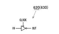
図7A及び図7Bはそれぞれ、本クロックドインバータ620、630のシンボル及び内部構成を示す回路図である。図7Aに示したシンボルはクロックドインバータの簡略的なシンボルを示しており、図6ではこのシンボルを使用している。
7A and 7B are circuit diagrams showing symbols and internal configurations of the clocked
図7Aに示したシンボルが表す回路構成をさらに詳細に示したのが図7Bに示した回路である。 The circuit shown in FIG. 7B shows the circuit configuration represented by the symbol shown in FIG. 7A in further detail.
図7Bを参照すると、クロックドインバータは、電源電圧と接地との間にPMOSトランジスタ704、705及びNMOSトランジスタ706、707が直列に接続されており、PMOSトランジスタ704はゲートにクロックCLOCKが入力され、NMOSトランジスタ707にはインバータ703で反転されたクロックがゲートに入力される。また、PMOSトランジスタ705及びNMOSトランジスタ706のゲートには入力信号INが印加される。
Referring to FIG.7B, the clocked inverter has
このようなクロックドインバータはクロック信号CLOCKがLの場合にのみインバータの役割を行い、クロック信号CLOCKがHの場合には出力がフローティング状態となってインバータとして動作しない。 Such a clocked inverter acts as an inverter only when the clock signal CLOCK is L, and when the clock signal CLOCK is H, the output is in a floating state and does not operate as an inverter.
すなわち、クロックCLOCKがLの場合には、PMOSトランジスタ704とNMOSトランジスタ707がターンオンされるので、通常のインバータとしての動作を行い、クロックCLOCKがHである場合にはPMOSトランジスタ704とNMOSトランジスタ707とがターンオフされるので、出力がフローティング状態となる。
That is, when the clock CLOCK is L, the
図7A及び7Bに示すような構造を有するクロックドインバータが図6に示される入出力マルチプレクサに用いられるため、MOB<0>ラインとMOB<1>ラインはクロックドインバータのゲート端、さらに詳細に述べると、図7Bに図示されるPMOSトランジスタ705のゲートとNMOSトランジスタのゲート706に入力されるため、MOBラインとラッチ640との間に電荷共有が生じない。
Since the clocked inverter having the structure shown in FIGS. 7A and 7B is used for the input / output multiplexer shown in FIG. 6, the MOB <0> and MOB <1> lines are the gate ends of the clocked inverter, In other words, since the signal is input to the gate of the
図8は、図5に示した、スタティックタイプに構成された入出力書き込み部507の詳細構成を示す回路図であって、ダブルデータレート同期式DRAM(Double Data Rate Synchronous Dynamic Random Access Memory: DDR SDRAM)に適用される回路図である。
FIG. 8 is a circuit diagram showing a detailed configuration of the input /
図8を参照すると、本入出力書き込み部507は、従来のダイナミックタイプと異なり、電源電圧VCCと接地電圧VSSとの間のダイレクトパス(direct path)をなくしたスタティックタイプに構成されている。
Referring to FIG. 8, unlike the conventional dynamic type, the input /
スタティックタイプに構成された本入出力書き込み部507は、入力されたデータが制御信号によって選択的に出力される伝送ゲート部820と、伝送ゲート部820の出力をDINBラインに伝達するための駆動部830及び伝送ゲート部820及び駆動部830を制御するための信号を発生する制御部840とから構成されている。
The input /
ここで、伝送ゲート部820は、DIN_R<0>信号を受信する伝送ゲート802とDIN_F<0>信号を受信する伝送ゲート803とからなり、伝送ゲート820部は、制御信号である偶数/奇数信号によってDIN_R<0>信号とDIN_F<0>信号のうち、いずれか一方を出力する。
Here, the
制御部840は、DINST信号を受信してこれを反転して出力するインバータ800と、インバータ800の出力を反転して出力するインバータ801と、偶数/奇数信号EV/ODを受信してこれを反転して出力するインバータ804とから構成されている。
The
駆動部830は、伝送ゲート部820の出力を受信してこれを反転して出力するクロックドインバータ805と、クロックドインバータ805の出力をラッチするインバータ807及びクロックドインバータ806と、クロックドインバータ805の出力を反転して出力するクロックドインバータ808と、クロックドインバータ808の出力をラッチするインバータ810及びクロックドインバータ809とから構成されている。
The driving
図8において、DINST信号は、データ入力ストローブ(input data strobe)信号であって、DINST信号に同期して、DIN_R<0>信号またはDIN_F<0>信号のうち、いずれか一方の信号が愚数/奇数信号EV/ODに応じてDINBラインに出力される。 In FIG. 8, the DINST signal is a data input strobe signal, and one of the DIN_R <0> signal and the DIN_F <0> signal is an odd number in synchronization with the DINST signal. Output to DINB line according to / odd signal EV / OD.
また、愚数/奇数信号EV/ODはDDR SDRAMで愚数、奇数を意味する信号であり、DIN_R<0>信号はクロックの立ち上がりエッジに同期する信号を意味し、DIN_F<0>信号はクロックの立下りエッジに同期する信号を意味する。 Further, the odd / odd signal EV / OD is a signal which means a odd / odd number in the DDR SDRAM, the DIN_R <0> signal is a signal synchronized with a rising edge of the clock, and the DIN_F <0> signal is a clock. Means a signal synchronized with the falling edge of.
愚数/奇数信号EV/ODがHの場合には、DIN_F<0>信号がクロックドインバータ805への入力となり、愚数/奇数信号EV/ODがLの場合にはDIN_R<0>信号がクロックドインバータ805への入力となる。
When the odd / odd signal EV / OD is H, the DIN_F <0> signal becomes an input to the clocked
この点を考慮して、愚数/奇数信号EV/ODがHであり、DINST信号がLからHに活性化される時、スタティックタイプに構成された入出力書き込み部507の動作を説明する。
In consideration of this point, the operation of the input /
まず、DINST信号及び反転されたDINST信号は、図8に示されたクロックドインバータ805、806、808、809のクロック入力として用いられている。したがって、DINST信号がLの場合にはクロックドインバータ805、809は動作状態となり、クロックドインバータ806、808はフローティング状態となる。
First, the DINST signal and the inverted DINST signal are used as clock inputs of the clocked
また、DINST信号がHの場合にはクロックドインバータ805、809はフローティング状態となり、クロックドインバータ806、808は動作状態となる。
When the DINST signal is H, the clocked
図8に示された入出力書き込み部507はDINST信号がLである場合、データを予め読み出してラッチし、DINST信号がHに活性化されると、予めラッチしていたデータをDINBラインに出力する。
When the DINST signal is L, the input /
すなわち、愚数/奇数EV/ODがHであり、DINST信号がLの場合には、クロックドインバータ805が動作状態となるので、反転されたDIN_F<0>信号がクロックドインバータ805の出力となる。
That is, when the odd / odd EV / OD is H and the DINST signal is L, the clocked
しかし、DINST信号がLである場合、クロックドインバータ808はフローティング状態となるので、クロックドインバータ805の出力である反転されたDIN_F<0>信号はクロックドインバータ808の出力に影響を与えることは無い。
However, when the DINST signal is L, the clocked
そして、DINST信号がLである場合、クロックドインバータ809は動作状態となるので、ターンオンされたクロックドインバータ809はインバータ810とともにDINB<0>ラインの値を現在の状態に維持するラッチの役割をする。
Then, when the DINST signal is L, the clocked
次いで、DINST信号がLからHに活性化されると、クロックドインバータ806及びクロックドインバータ808は動作状態となり、クロックドインバータ805及びクロックドインバータ809はフローティング状態となる。
Next, when the DINST signal is activated from L to H, the clocked
このように、クロックドインバータ808が動作状態となるので、クロックドインバータ805の出力である反転されたDIN_F<0>信号がクロックドインバータ808に入力され、クロックドインバータ808がDIN_F<0>信号を出力する。
As described above, since the clocked
このように、DINST信号がLからHに活性化されると、クロックドインバータ806が動作状態となるので、クロックドインバータ806はインバータ807とともにクロックドインバータ808を駆動する。その結果、DINB<0>ラインにはインバータ810を経て反転されたDIN_F<0>信号が出力される。
As described above, when the DINST signal is activated from L to H, the clocked
また、DINST信号がHからLに遷移する場合には、クロックドインバータ809が動作状態となるので、クロックドインバータ809はインバータ810とともにDINB<0>ラインに出力された信号を維持するラッチ回路として機能する。
Further, when the DINST signal transitions from H to L, the clocked
このように本発明の実施の形態に係るメモリ素子は、入出力書き込み部の構成をスタティックタイプの回路に変更したので、従来に比べて電流消費を減少させることができ、対称にレイアウトしなければならない問題も避けることができる長所がある。 As described above, in the memory element according to the embodiment of the present invention, the configuration of the input / output write unit is changed to a static type circuit, so that the current consumption can be reduced as compared with the related art, and unless the layout is symmetrical There is an advantage that the problem that can be avoided can be avoided.
以下、図5ないし図8を参照して、本発明の実施の形態に係るメモリ素子におけるデータの読み出し/書き込み動作について説明すると、以下の通りである。 Hereinafter, the data read / write operation in the memory device according to the embodiment of the present invention will be described with reference to FIG. 5 to FIG.
まず、N-1番目のクロックでHデータを読み出す場合に、セルに格納されたHデータは、ビットライン感知増幅器500を経てメイン増幅器501から出力され、読み出し動作で用いられるMOBライン503を通して入出力マルチプレクサ506に入力される。
First, when reading the H data at the (N-1) th clock, the H data stored in the cell is output from the
Hデータを読み出す動作であるため、図6に示した入出力マルチプレクサ506において、MOB<0>またはMOB<1>のいずれかがクロックドインバータ620またはクロックドインバータ630を通過して入出力マルチプレクサ506の出力となる。そして入出力マルチプレクサ506の出力端子MX_OUTに接続されたラッチ640はこのHデータをラッチする。
Since the operation is to read H data, in the input /
このような読み出し動作時にクロックドインバータ620、またはクロックドインバータ630のいずれかが動作状態となっても、MOBライン503はクロックドインバータを構成しているトランジスタのゲートに入力されているので、MOBライン503とラッチ640との間の電荷共有現象は発生しない。
Even if either the clocked
次いで、N番目のクロックでLデータを書き込む場合には、Lデータはデータ入力ドライバー(図示せず)を通して入出力書き込み部507に入力され、入出力書き込み部507は入力されたデータをDINBライン504に出力する。DINBライン504に出力されたデータは書き込みドライバー502に入力された後、ビットライン感知増幅器500を経てセルに格納される。
Next, when writing L data at the Nth clock, the L data is input to the input /
書き込み動作であるため、WT信号はHであり、図6に示したNANDゲート606、607の出力は全部Hになる。したがって、クロックドインバータ620、630の出力は全部フローティング状態となるので、ラッチ640の出力に影響を与えない。したがって、ラッチ640はN-1番目のクロックで読み出したHデータをラッチしたままである。
Since this is a write operation, the WT signal is H, and the outputs of the
次いで、N+1番目のクロックでLデータを読み出す場合、セルに格納されたLデータはビットライン感知増幅器500、メイン増幅器501、MOBライン503及び入出力マルチプレクサ506を経由して出力される。
Next, when reading L data at the (N + 1) th clock, the L data stored in the cell is output via the bit
読み出し動作であるため、入出力マルチプレクサ506に備えられたクロックドインバータ608、またはクロックドインバータ609は動作状態となってMOBライン503に出力されたLデータを出力する。
Since the read operation is performed, the clocked inverter 608 or the clocked inverter 609 provided in the input /
この場合、入出力マルチプレクサ506の出力端子MX_OUTに接続されたラッチ640は、N番目のクロックでHデータをラッチしていたが、N+1番目のクロックではLデータをラッチするようになる。
In this case, the
このように読み出し動作時にMOBライン及びラッチ640の間の電荷共有が発生しないことは前述したのと同様であり、本発明の実施の形態に係るメモリ素子ではリピータ505をMOBライン503に接続して用いてもデータエラーが発生しない。
As described above, no charge sharing occurs between the MOB line and the
また、本発明の実施の形態に係るメモリ素子では、従来のグローバル入出力ラインを読み出し動作時に使用するMOBラインと書き込み動作時に使用するDINBラインとに分離しているので、MOBラインとDINBラインとを交互に使用してルーチングでき、従来GIOラインがトグリング(toggling)されることで生じていたカップリングノイズ(coupling noise)を減少させることができる。 In the memory device according to the embodiment of the present invention, the conventional global input / output line is separated into a MOB line used during a read operation and a DINB line used during a write operation. Can be alternately used to reduce the coupling noise that has conventionally been caused by the toggling of the GIO line.
すなわち、MOBラインとDINBラインとを交互にルーチングすれば、例えばMOBラインを利用した読み出し動作時には、DINBラインはH、またはLに固定された値を有しているため、非常に優れた遮蔽(Shilding)効果を有することができ、これによって、カップリングノイズイミュニティが特に弱いリピータを使用してもカップリングノイズイミュニティを増大させることができる。 That is, if the MOB line and the DINB line are alternately routed, for example, at the time of the read operation using the MOB line, the DINB line has a value fixed to H or L, so that a very excellent shielding ( In this case, the coupling noise immunity can be increased even when a repeater having particularly weak coupling noise immunity is used.
本発明の実施の形態では、信号伝達速度を増加させるために、MOBラインにのみリピータを接続する場合を説明したが、DINBラインにもリピータを接続してもよい。 In the embodiment of the present invention, a case has been described where a repeater is connected only to the MOB line in order to increase the signal transmission speed. However, a repeater may be connected to the DINB line.
なお、本発明は、上記の実施の形態として開示した範囲に限定されるものではない。本発明に係る技術的思想から逸脱しない範囲内で種々の改良、変更が可能であり、それらも本発明の技術的範囲に属する。 Note that the present invention is not limited to the scope disclosed in the above embodiment. Various improvements and modifications can be made without departing from the technical concept of the present invention, and these also belong to the technical scope of the present invention.
500 ビットライン感知増幅器
501 メイン増幅器
502 書き込みドライバー
503 MOBライン
504 DINBライン
506 入出力マルチプレクサ
507 入出力書き込み部
500 bit line sense amplifier
501 Main Amplifier
502 Write Driver
503 MOB line
504 DINB line
506 I / O multiplexer
507 I / O writing unit
Claims (9)
前記第1データラインに接続された入出力マルチプレクサと、
前記第1データラインに接続された第1リピータと、
入力される書き込みデータを第2データラインに出力する入出力書き込み部と、
前記第2データラインに接続され、前記第2データラインに出力されたデータを前記ビットライン感知増幅器に出力する書き込みドライバーと
を備えていることを特徴とするメモリ素子。 A main amplifier for amplifying the output of the bit line sense amplifier and outputting the amplified data to the first data line;
An input / output multiplexer connected to the first data line;
A first repeater connected to the first data line;
An input / output writing unit that outputs input write data to a second data line,
A write driver connected to the second data line and outputting data output to the second data line to the bit line sense amplifier.
前記第1データラインが入力されるクロックドインバータと、該クロックドインバータの出力端子に接続されたラッチとを備えて構成され、
前記ラッチに格納されたデータ及び前記第1データラインの間の電荷共有を阻止することを特徴とする請求項1に記載のメモリ素子。 The input / output multiplexer comprises:
A clocked inverter to which the first data line is input, and a latch connected to an output terminal of the clocked inverter,
2. The memory device according to claim 1, wherein charge sharing between the data stored in the latch and the first data line is prevented.
アドレス信号、モード信号及び書き込み動作時に活性化されるイネーブル信号を受信し、前記クロックドインバータを制御するための制御信号を出力する制御部をさらに備えていることを特徴とする請求項2に記載のメモリ素子。 The input / output multiplexer comprises:
3. The control unit according to claim 2, further comprising: a control unit that receives an address signal, a mode signal, and an enable signal activated during a write operation, and outputs a control signal for controlling the clocked inverter. Memory element.
入力されるアドレス信号を反転させて出力する第1インバータと、
前記モード信号及び前記第1インバータの出力が入力される第1NANDゲートと、
前記モード信号及び前記アドレス信号が入力される第2NANDゲートと、
書き込み動作時に活性化される前記イネーブル信号を反転して出力する第2インバータと、
前記第2NANDゲートの出力を反転して出力する第3インバータと、
前記第1NANDゲートの出力を反転して出力する第4インバータと、
前記第2インバータの出力及び前記第3インバータの出力が入力される第3NANDゲートと、
前記第2インバータの出力及び前記第4インバータの出力が入力される第4NANDゲートと
を備えていることを特徴とする請求項3に記載のメモリ素子。 The control unit includes:
A first inverter that inverts and outputs an input address signal,
A first NAND gate to which the mode signal and the output of the first inverter are input;
A second NAND gate to which the mode signal and the address signal are input;
A second inverter that inverts and outputs the enable signal activated during a write operation;
A third inverter that inverts and outputs the output of the second NAND gate;
A fourth inverter that inverts and outputs the output of the first NAND gate;
A third NAND gate to which an output of the second inverter and an output of the third inverter are input;
4. The memory device according to claim 3, further comprising: a fourth NAND gate to which an output of the second inverter and an output of the fourth inverter are input.
入力されたデータを選択的に出力する伝送ゲート部と、
該伝送ゲート部の出力を第2データラインに伝達する駆動部と、
前記伝送ゲート部及び前記駆動部を制御する信号を発生する制御部とを備え、
クロックドインバータを備えてスタティックタイプに構成されていることを特徴とする請求項1に記載のメモリ素子。 The input / output writing unit,
A transmission gate unit for selectively outputting input data,
A driver for transmitting an output of the transmission gate unit to a second data line;
A control unit that generates a signal for controlling the transmission gate unit and the driving unit,
2. The memory device according to claim 1, wherein the memory device is configured as a static type including a clocked inverter.
入力されるデータ入力ストローブ信号を反転して出力する第10インバータと、
該第10インバータの出力を反転して出力する第11インバータと、
入力される偶数/奇数信号を反転して出力する第12インバータと
を備えていることを特徴とする請求項5に記載のメモリ素子。 The control unit includes:
A tenth inverter that inverts and outputs the input data input strobe signal,
An eleventh inverter that inverts and outputs the output of the tenth inverter,
6. The memory device according to claim 5, further comprising: a twelfth inverter that inverts and outputs an even / odd signal that is input.
前記伝送ゲート部の出力を反転して出力する第1クロックドインバータと、
該第1クロックドインバータの出力をラッチする第12インバータ及び第2クロックドインバータと、
前記第1クロックドインバータの出力を反転して出力する第3クロックドインバータと、
該第3クロックドインバータの出力をラッチする第13インバータ及び第4クロックドインバータとを備え、
前記第1〜第4クロックドインバータが、前記第10インバータ及び第11インバータの出力を制御信号として受信することを特徴とする請求項6に記載のメモリ素子。 The driving unit is
A first clocked inverter that inverts and outputs the output of the transmission gate unit,
A twelfth inverter and a second clocked inverter that latch the output of the first clocked inverter;
A third clocked inverter that inverts and outputs the output of the first clocked inverter,
A thirteenth inverter that latches the output of the third clocked inverter and a fourth clocked inverter,
7. The memory device according to claim 6, wherein the first to fourth clocked inverters receive outputs of the tenth and eleventh inverters as control signals.
Applications Claiming Priority (1)
| Application Number | Priority Date | Filing Date | Title |
|---|---|---|---|
| KR10-2003-0034876A KR100492907B1 (en) | 2003-05-30 | 2003-05-30 | Memory device with modified global input output scheme |
Publications (1)
| Publication Number | Publication Date |
|---|---|
| JP2004362744A true JP2004362744A (en) | 2004-12-24 |
Family
ID=33448312
Family Applications (1)
| Application Number | Title | Priority Date | Filing Date |
|---|---|---|---|
| JP2004103091A Pending JP2004362744A (en) | 2003-05-30 | 2004-03-31 | Memory element |
Country Status (4)
| Country | Link |
|---|---|
| US (1) | US6920068B2 (en) |
| JP (1) | JP2004362744A (en) |
| KR (1) | KR100492907B1 (en) |
| TW (1) | TWI312158B (en) |
Families Citing this family (9)
| Publication number | Priority date | Publication date | Assignee | Title |
|---|---|---|---|---|
| KR100515070B1 (en) * | 2003-12-01 | 2005-09-16 | 주식회사 하이닉스반도체 | Semiconductor memory device |
| KR100618697B1 (en) * | 2004-04-28 | 2006-09-08 | 주식회사 하이닉스반도체 | Scheme of the data transmission lins of a memory device |
| US7525341B1 (en) * | 2004-09-20 | 2009-04-28 | Marvell Israel (M.I.S.L.) Ltd. | Time-balanced multiplexer switching methods and apparatus |
| US7652516B2 (en) | 2006-10-20 | 2010-01-26 | Marvell Israel (M.I.S.L.) Ltd. | Apparatus and method for generating a clock signal |
| KR100842743B1 (en) * | 2006-10-27 | 2008-07-01 | 주식회사 하이닉스반도체 | Semiconductor device with high density |
| KR100931023B1 (en) | 2007-11-02 | 2009-12-10 | 주식회사 하이닉스반도체 | Semiconductor memory device |
| US8058900B1 (en) | 2008-04-14 | 2011-11-15 | Marvell Israel (M.I.S.L) Ltd. | Method and apparatus for clocking |
| KR101984213B1 (en) | 2018-01-04 | 2019-05-30 | 경상대학교산학협력단 | Polymer composite and preparation method thereof |
| KR102542527B1 (en) * | 2018-03-23 | 2023-06-09 | 에스케이하이닉스 주식회사 | Data transfer device and semiconductor device including the same |
Citations (14)
| Publication number | Priority date | Publication date | Assignee | Title |
|---|---|---|---|---|
| JPH025283A (en) * | 1988-06-21 | 1990-01-10 | Mitsubishi Electric Corp | Semiconductor memory |
| JPH08335394A (en) * | 1995-03-28 | 1996-12-17 | Lg Semicon Co Ltd | Data transmission equipment of memory |
| JPH09106679A (en) * | 1995-09-11 | 1997-04-22 | Samsung Electron Co Ltd | Semiconductor memory device |
| JPH1027473A (en) * | 1996-07-11 | 1998-01-27 | Nec Corp | Semiconductor memory |
| JPH11273335A (en) * | 1997-12-10 | 1999-10-08 | Texas Instr Inc <Ti> | High-speed, broad-band random access memory |
| JP2000182370A (en) * | 1998-12-16 | 2000-06-30 | Toshiba Corp | Semiconductor memory |
| JP2000195255A (en) * | 1998-12-28 | 2000-07-14 | Samsung Electronics Co Ltd | Memory device |
| JP2000306383A (en) * | 1999-04-08 | 2000-11-02 | Samsung Electronics Co Ltd | Memory provided with input/output sense amplifier with variable-current gain characteristic |
| JP2001067900A (en) * | 1999-07-23 | 2001-03-16 | Samsung Electronics Co Ltd | Semiconductor memory externally controllable in data input/output mode |
| JP2001084766A (en) * | 2000-08-15 | 2001-03-30 | Hitachi Ltd | Semiconductor device |
| JP2001160289A (en) * | 1999-10-27 | 2001-06-12 | Samsung Electronics Co Ltd | Semiconductor memory |
| JP2001250385A (en) * | 2000-03-03 | 2001-09-14 | Mitsubishi Electric Corp | Semiconductor storage device |
| US20030101323A1 (en) * | 2001-11-26 | 2003-05-29 | Chul-Soo Kim | Synchronous semiconductor memory device having multi-bank scheme |
| JP2004335091A (en) * | 2003-05-07 | 2004-11-25 | Samsung Electronics Co Ltd | Semiconductor device and method for outputting and inputting data simultaneously through single pad |
Family Cites Families (16)
| Publication number | Priority date | Publication date | Assignee | Title |
|---|---|---|---|---|
| US5384745A (en) * | 1992-04-27 | 1995-01-24 | Mitsubishi Denki Kabushiki Kaisha | Synchronous semiconductor memory device |
| US5594704A (en) * | 1992-04-27 | 1997-01-14 | Mitsubishi Denki Kabushiki Kaisha | Synchronous semiconductor memory device |
| JP3577112B2 (en) | 1994-09-08 | 2004-10-13 | 株式会社ルネサステクノロジ | Synchronous semiconductor memory device |
| JPH08278916A (en) * | 1994-11-30 | 1996-10-22 | Hitachi Ltd | Multichannel memory system, transfer information synchronizing method, and signal transfer circuit |
| JPH08221981A (en) | 1994-12-15 | 1996-08-30 | Mitsubishi Electric Corp | Synchronous type semiconductor memory |
| JPH0973776A (en) * | 1995-09-07 | 1997-03-18 | Mitsubishi Electric Corp | Synchronous semiconductor memory |
| JPH09288888A (en) * | 1996-04-22 | 1997-11-04 | Mitsubishi Electric Corp | Semiconductor memory |
| JPH11317091A (en) | 1998-04-30 | 1999-11-16 | Nec Corp | Semiconductor storage device |
| JP2000076858A (en) | 1998-08-31 | 2000-03-14 | Hitachi Ltd | Semiconductor device |
| JP4462663B2 (en) | 1998-09-10 | 2010-05-12 | 株式会社ルネサステクノロジ | Semiconductor memory device |
| KR100363079B1 (en) * | 1999-02-01 | 2002-11-30 | 삼성전자 주식회사 | Multi-bank memory device having shared IO sense amplifier by adjacent memory banks |
| KR100341576B1 (en) | 1999-06-28 | 2002-06-22 | 박종섭 | Method and device for controlling of pipedata input of semiconductor memory device |
| JP2001126470A (en) | 1999-10-26 | 2001-05-11 | Mitsubishi Electric Corp | Semiconductor memory |
| JP2001155485A (en) | 1999-11-29 | 2001-06-08 | Mitsubishi Electric Corp | Semiconductor memory |
| KR100385956B1 (en) | 2001-02-14 | 2003-06-02 | 삼성전자주식회사 | Semiconductor memory device having effective column redundancy scheme |
| KR100543915B1 (en) * | 2003-05-16 | 2006-01-23 | 주식회사 하이닉스반도체 | Data input circuit in memory device |
-
2003
- 2003-05-30 KR KR10-2003-0034876A patent/KR100492907B1/en not_active IP Right Cessation
- 2003-12-30 TW TW092137420A patent/TWI312158B/en not_active IP Right Cessation
- 2003-12-31 US US10/749,892 patent/US6920068B2/en not_active Expired - Lifetime
-
2004
- 2004-03-31 JP JP2004103091A patent/JP2004362744A/en active Pending
Patent Citations (15)
| Publication number | Priority date | Publication date | Assignee | Title |
|---|---|---|---|---|
| JPH025283A (en) * | 1988-06-21 | 1990-01-10 | Mitsubishi Electric Corp | Semiconductor memory |
| JPH08335394A (en) * | 1995-03-28 | 1996-12-17 | Lg Semicon Co Ltd | Data transmission equipment of memory |
| JPH09106679A (en) * | 1995-09-11 | 1997-04-22 | Samsung Electron Co Ltd | Semiconductor memory device |
| JPH1027473A (en) * | 1996-07-11 | 1998-01-27 | Nec Corp | Semiconductor memory |
| JPH11273335A (en) * | 1997-12-10 | 1999-10-08 | Texas Instr Inc <Ti> | High-speed, broad-band random access memory |
| JP2000182370A (en) * | 1998-12-16 | 2000-06-30 | Toshiba Corp | Semiconductor memory |
| JP2000195255A (en) * | 1998-12-28 | 2000-07-14 | Samsung Electronics Co Ltd | Memory device |
| JP2000306383A (en) * | 1999-04-08 | 2000-11-02 | Samsung Electronics Co Ltd | Memory provided with input/output sense amplifier with variable-current gain characteristic |
| JP2001067900A (en) * | 1999-07-23 | 2001-03-16 | Samsung Electronics Co Ltd | Semiconductor memory externally controllable in data input/output mode |
| JP2001160289A (en) * | 1999-10-27 | 2001-06-12 | Samsung Electronics Co Ltd | Semiconductor memory |
| JP2001250385A (en) * | 2000-03-03 | 2001-09-14 | Mitsubishi Electric Corp | Semiconductor storage device |
| JP2001084766A (en) * | 2000-08-15 | 2001-03-30 | Hitachi Ltd | Semiconductor device |
| US20030101323A1 (en) * | 2001-11-26 | 2003-05-29 | Chul-Soo Kim | Synchronous semiconductor memory device having multi-bank scheme |
| JP2003187574A (en) * | 2001-11-26 | 2003-07-04 | Samsung Electronics Co Ltd | Synchronous semiconductor memory device |
| JP2004335091A (en) * | 2003-05-07 | 2004-11-25 | Samsung Electronics Co Ltd | Semiconductor device and method for outputting and inputting data simultaneously through single pad |
Also Published As
| Publication number | Publication date |
|---|---|
| TW200426852A (en) | 2004-12-01 |
| KR100492907B1 (en) | 2005-06-02 |
| US6920068B2 (en) | 2005-07-19 |
| TWI312158B (en) | 2009-07-11 |
| KR20040103003A (en) | 2004-12-08 |
| US20040240274A1 (en) | 2004-12-02 |
Similar Documents
| Publication | Publication Date | Title |
|---|---|---|
| KR100543915B1 (en) | Data input circuit in memory device | |
| US6950370B2 (en) | Synchronous memory device for preventing erroneous operation due to DQS ripple | |
| KR100240539B1 (en) | Synchronous semiconductor memory device in which current consumed by input buffer circuit is reduced | |
| JP2000132967A (en) | Device for buffering data strobe signal with high speed memory element | |
| US7352650B2 (en) | External clock synchronization semiconductor memory device and method for controlling same | |
| JP3953691B2 (en) | Integrated circuit and synchronous semiconductor memory device | |
| JP2008171546A (en) | Semiconductor memory device and its driving method | |
| US7593275B2 (en) | Semiconductor memory device | |
| US7173864B2 (en) | Data latch circuit and semiconductor device using the same | |
| US20060176078A1 (en) | Voltage level shifting circuit and method | |
| JP3685709B2 (en) | Synchronous memory device and continuous reading method thereof | |
| JP2015012351A (en) | Semiconductor device | |
| JP2004362744A (en) | Memory element | |
| WO2015079608A1 (en) | Semiconductor storage device | |
| JP5763659B2 (en) | Semiconductor memory device | |
| US7512019B2 (en) | High speed digital signal input buffer and method using pulsed positive feedback | |
| US6456543B1 (en) | Data input/output circuit for semiconductor memory device | |
| KR20200027044A (en) | Input buffer circuit | |
| JP2004032284A (en) | Semiconductor integrated circuit | |
| KR100990139B1 (en) | Memory device with improved repeater | |
| US11276468B2 (en) | High-speed efficient level shifter | |
| KR20080003049A (en) | Column control circuit for data input/output section control | |
| JP3192709B2 (en) | Semiconductor storage device | |
| KR19990070830A (en) | Address transition detection circuit | |
| JP2004247566A (en) | Semiconductor storage device |
Legal Events
| Date | Code | Title | Description |
|---|---|---|---|
| A621 | Written request for application examination |
Free format text: JAPANESE INTERMEDIATE CODE: A621 Effective date: 20060126 |
|
| A977 | Report on retrieval |
Free format text: JAPANESE INTERMEDIATE CODE: A971007 Effective date: 20081006 |
|
| A131 | Notification of reasons for refusal |
Free format text: JAPANESE INTERMEDIATE CODE: A131 Effective date: 20081119 |
|
| A521 | Written amendment |
Free format text: JAPANESE INTERMEDIATE CODE: A523 Effective date: 20090219 |
|
| A131 | Notification of reasons for refusal |
Free format text: JAPANESE INTERMEDIATE CODE: A131 Effective date: 20100120 |
|
| A521 | Written amendment |
Free format text: JAPANESE INTERMEDIATE CODE: A523 Effective date: 20100420 |
|
| A02 | Decision of refusal |
Free format text: JAPANESE INTERMEDIATE CODE: A02 Effective date: 20101214 |