JP5763659B2 - Semiconductor memory device - Google Patents
Semiconductor memory device Download PDFInfo
- Publication number
- JP5763659B2 JP5763659B2 JP2012536153A JP2012536153A JP5763659B2 JP 5763659 B2 JP5763659 B2 JP 5763659B2 JP 2012536153 A JP2012536153 A JP 2012536153A JP 2012536153 A JP2012536153 A JP 2012536153A JP 5763659 B2 JP5763659 B2 JP 5763659B2
- Authority
- JP
- Japan
- Prior art keywords
- memory device
- semiconductor memory
- write
- bit line
- data
- Prior art date
- Legal status (The legal status is an assumption and is not a legal conclusion. Google has not performed a legal analysis and makes no representation as to the accuracy of the status listed.)
- Expired - Fee Related
Links
Images


Classifications
-
- G—PHYSICS
- G11—INFORMATION STORAGE
- G11C—STATIC STORES
- G11C8/00—Arrangements for selecting an address in a digital store
- G11C8/08—Word line control circuits, e.g. drivers, boosters, pull-up circuits, pull-down circuits, precharging circuits, for word lines
-
- G—PHYSICS
- G11—INFORMATION STORAGE
- G11C—STATIC STORES
- G11C11/00—Digital stores characterised by the use of particular electric or magnetic storage elements; Storage elements therefor
- G11C11/21—Digital stores characterised by the use of particular electric or magnetic storage elements; Storage elements therefor using electric elements
- G11C11/34—Digital stores characterised by the use of particular electric or magnetic storage elements; Storage elements therefor using electric elements using semiconductor devices
- G11C11/40—Digital stores characterised by the use of particular electric or magnetic storage elements; Storage elements therefor using electric elements using semiconductor devices using transistors
- G11C11/41—Digital stores characterised by the use of particular electric or magnetic storage elements; Storage elements therefor using electric elements using semiconductor devices using transistors forming static cells with positive feedback, i.e. cells not needing refreshing or charge regeneration, e.g. bistable multivibrator or Schmitt trigger
- G11C11/413—Auxiliary circuits, e.g. for addressing, decoding, driving, writing, sensing, timing or power reduction
- G11C11/417—Auxiliary circuits, e.g. for addressing, decoding, driving, writing, sensing, timing or power reduction for memory cells of the field-effect type
- G11C11/419—Read-write [R-W] circuits
-
- G—PHYSICS
- G11—INFORMATION STORAGE
- G11C—STATIC STORES
- G11C11/00—Digital stores characterised by the use of particular electric or magnetic storage elements; Storage elements therefor
- G11C11/02—Digital stores characterised by the use of particular electric or magnetic storage elements; Storage elements therefor using magnetic elements
- G11C11/16—Digital stores characterised by the use of particular electric or magnetic storage elements; Storage elements therefor using magnetic elements using elements in which the storage effect is based on magnetic spin effect
- G11C11/165—Auxiliary circuits
- G11C11/1653—Address circuits or decoders
-
- G—PHYSICS
- G11—INFORMATION STORAGE
- G11C—STATIC STORES
- G11C11/00—Digital stores characterised by the use of particular electric or magnetic storage elements; Storage elements therefor
- G11C11/02—Digital stores characterised by the use of particular electric or magnetic storage elements; Storage elements therefor using magnetic elements
- G11C11/16—Digital stores characterised by the use of particular electric or magnetic storage elements; Storage elements therefor using magnetic elements using elements in which the storage effect is based on magnetic spin effect
- G11C11/165—Auxiliary circuits
- G11C11/1675—Writing or programming circuits or methods
-
- G—PHYSICS
- G11—INFORMATION STORAGE
- G11C—STATIC STORES
- G11C11/00—Digital stores characterised by the use of particular electric or magnetic storage elements; Storage elements therefor
- G11C11/02—Digital stores characterised by the use of particular electric or magnetic storage elements; Storage elements therefor using magnetic elements
- G11C11/16—Digital stores characterised by the use of particular electric or magnetic storage elements; Storage elements therefor using magnetic elements using elements in which the storage effect is based on magnetic spin effect
- G11C11/165—Auxiliary circuits
- G11C11/1693—Timing circuits or methods
-
- G—PHYSICS
- G11—INFORMATION STORAGE
- G11C—STATIC STORES
- G11C7/00—Arrangements for writing information into, or reading information out from, a digital store
- G11C7/12—Bit line control circuits, e.g. drivers, boosters, pull-up circuits, pull-down circuits, precharging circuits, equalising circuits, for bit lines
-
- G—PHYSICS
- G11—INFORMATION STORAGE
- G11C—STATIC STORES
- G11C11/00—Digital stores characterised by the use of particular electric or magnetic storage elements; Storage elements therefor
- G11C11/02—Digital stores characterised by the use of particular electric or magnetic storage elements; Storage elements therefor using magnetic elements
- G11C11/16—Digital stores characterised by the use of particular electric or magnetic storage elements; Storage elements therefor using magnetic elements using elements in which the storage effect is based on magnetic spin effect
-
- G—PHYSICS
- G11—INFORMATION STORAGE
- G11C—STATIC STORES
- G11C11/00—Digital stores characterised by the use of particular electric or magnetic storage elements; Storage elements therefor
- G11C11/21—Digital stores characterised by the use of particular electric or magnetic storage elements; Storage elements therefor using electric elements
- G11C11/34—Digital stores characterised by the use of particular electric or magnetic storage elements; Storage elements therefor using electric elements using semiconductor devices
- G11C11/40—Digital stores characterised by the use of particular electric or magnetic storage elements; Storage elements therefor using electric elements using semiconductor devices using transistors
- G11C11/401—Digital stores characterised by the use of particular electric or magnetic storage elements; Storage elements therefor using electric elements using semiconductor devices using transistors forming cells needing refreshing or charge regeneration, i.e. dynamic cells
- G11C11/4063—Auxiliary circuits, e.g. for addressing, decoding, driving, writing, sensing or timing
- G11C11/407—Auxiliary circuits, e.g. for addressing, decoding, driving, writing, sensing or timing for memory cells of the field-effect type
- G11C11/409—Read-write [R-W] circuits
- G11C11/4091—Sense or sense/refresh amplifiers, or associated sense circuitry, e.g. for coupled bit-line precharging, equalising or isolating
Landscapes
- Engineering & Computer Science (AREA)
- Computer Hardware Design (AREA)
- Microelectronics & Electronic Packaging (AREA)
- Static Random-Access Memory (AREA)
- Dram (AREA)
Description
本発明は、半導体記憶装置、特にデータ書き込み時の非選択メモリセルのデータ破壊を防止しつつ高速動作を実現する半導体記憶装置に関するものである。 The present invention relates to a semiconductor memory device, and more particularly to a semiconductor memory device that realizes high-speed operation while preventing data destruction of unselected memory cells during data writing.
従来のSRAM(スタティック・ランダム・アクセス・メモリ)において、メモリセルを構成するトランジスタの微細化によってトランジスタ特性のばらつきが大きくなり、メモリ動作中に保持しているメモリセルデータが破壊されてしまう課題があった。 In conventional SRAM (Static Random Access Memory), there is a problem that the variation in transistor characteristics increases due to the miniaturization of the transistors constituting the memory cell, and the memory cell data held during the memory operation is destroyed. there were.
読み出し動作時のデータ破壊を防ぐ方法としてビット線を書き込み用と読み出し用とに分ける技術があった。また、書き込み動作時の非選択メモリセルのデータ破壊を防ぐ方法として、非選択メモリセルから読み出したデータを書き戻す技術があった(特許文献1及び2参照)。
As a method for preventing data destruction during a read operation, there has been a technique for dividing a bit line into one for writing and one for reading. In addition, as a method for preventing data destruction of unselected memory cells during a write operation, there is a technique for writing back data read from unselected memory cells (see
上記従来技術の半導体記憶装置における書き込み動作時のデータ破壊を解決する技術では、以下の課題があった。 The technique for solving the data destruction at the time of the write operation in the conventional semiconductor memory device has the following problems.
まず、書き込み動作時に非選択メモリセルへ一度読み出したデータを書き戻す動作を行うために、単純な書き込み動作及び読み出し動作に比べて動作時間が長いという課題があり、SRAMの動作を速くできないといった課題があった。 First, there is a problem that the operation time is longer than a simple write operation and a read operation in order to perform an operation of writing back data once read to a non-selected memory cell during a write operation, and the SRAM operation cannot be accelerated. was there.
次に、データを書き戻す動作を実現するために、従来の書き込み動作に使用していたライトバッファと同等の能力を持つ書き込み回路が必要であり、また正確な書き戻しタイミング制御が必要なために部品点数が増え、結果としてSRAMの回路面積が大きくなる課題があった。 Next, in order to realize the operation of writing back data, a writing circuit having the same capability as the write buffer used in the conventional writing operation is required, and accurate write back timing control is required. There is a problem that the number of parts increases, and as a result, the circuit area of the SRAM increases.
本発明は、上記課題を解決するものであって、書き込み用ビット線対のそれぞれのプリチャージ電位を、非選択メモリセルのデータに応じた電位レベルに設定する機能を備えることで、動作を高速化しつつメモリセルのデータ破壊を防止する半導体記憶装置を実現することを目的とする。 The present invention solves the above-described problem, and has a function of setting each precharge potential of a pair of write bit lines to a potential level according to data of a non-selected memory cell, thereby speeding up the operation. It is an object of the present invention to realize a semiconductor memory device that prevents data destruction of memory cells while reducing the size.
上記課題を解決するために、本発明に係る半導体記憶装置は、第1及び第2の回路要素によりデータを記憶するように構成されたデータ保持回路と、当該データ保持回路と読み出し用ビット線及び書き込み用ビット線対とを繋ぐように配置されたトランジスタを含む回路とで構成されたメモリセルと、読み出し用ビット線に繋がったデータ増幅器と、書き込み用ビット線対に各々繋がったプルダウントランジスタとを備え、データ増幅器の出力が一方のプルダウントランジスタのゲート電極に接続されて、他方のプルダウントランジスタのゲート電極に書き込み用ビット線対の一方が接続されていることを特徴とする。 In order to solve the above problems, a semiconductor memory device according to the present invention includes a data holding circuit configured to store data by first and second circuit elements, the data holding circuit, a read bit line, A memory cell including a transistor including a transistor arranged to connect the write bit line pair, a data amplifier connected to the read bit line, and a pull-down transistor connected to each of the write bit line pairs. And the output of the data amplifier is connected to the gate electrode of one pull-down transistor, and one of the write bit line pairs is connected to the gate electrode of the other pull-down transistor.
本発明により、書き込み用ビット線対のそれぞれのプリチャージ電位を、非選択メモリセルのデータに応じた電位レベルに設定する機能を備えることで、動作を高速化し、かつ小面積化を実現しつつ、メモリセルのデータ破壊を防止する半導体記憶装置を実現することができる。 According to the present invention, the function of setting each precharge potential of the write bit line pair to a potential level corresponding to the data of the non-selected memory cell is provided, and the operation is speeded up and the area is reduced. Therefore, it is possible to realize a semiconductor memory device that prevents data destruction of memory cells.
以下、本発明の実施形態を図面に基づいて詳細に説明する。なお、以下の各実施形態及び変形例において、他の実施形態及び変形例と同様の機能を有する構成要素については同一の符号を付して説明を省略する。 Hereinafter, embodiments of the present invention will be described in detail with reference to the drawings. In the following embodiments and modifications, components having the same functions as those of the other embodiments and modifications are denoted by the same reference numerals and description thereof is omitted.
《実施形態1》
本発明の実施形態1の半導体記憶装置に関して、具体的な例として図1、図2、図3、図4を用いながら説明する。
The semiconductor memory device according to the first embodiment of the present invention will be described with reference to FIGS. 1, 2, 3, and 4 as specific examples.
図1に示す半導体記憶装置は、マトリックス状に配置された複数のメモリセル1と、各メモリセル1に繋がる読み出し用ビット線RBLU0/RBLL0/RBLU1/RBLL1のデータを増幅するデータ増幅器2と、読み出しデータを使ってメモリセル1に繋がる書き込み用ビット線対WBL0/NWBL0;WBL1/NWBL1のプリチャージ電位を再設定する機能を持つプリチャージ電位再設定回路3と、これらデータ増幅器2及びプリチャージ電位再設定回路3を含みメモリセル1とメモリセル1との間に配置されたローカルアンプ回路4と、書き込み用ビット線対WBL0/NWBL0;WBL1/NWBL1の電源電位(VDDレベル又はHレベル)を一方のグランド電位(VSSレベル又はLレベル)を使って保持するキーパー回路5と、書き込み用ビット線対WBL0/NWBL0;WBL1/NWBL1に入力データDIを転送するためのライトバッファ6と、データ増幅器2からの出力データ線GRBL0/GRBL1をドライブして出力データDOを出力するための出力バッファ7と、これらキーパー回路5、ライトバッファ6及び出力バッファ7を含むI/F回路8と、メモリセル1の書き込み用ワード線WWL0/WWL1及び読み出し用ワード線RWL0/RWL1並びにローカルアンプ回路4で制御信号として使われる読み出し制御信号SE0/SE1及びプリチャージ電位再設定制御信号CA0/CA1を生成するロウデコーダ9と、クロック信号CLKに加えてアドレス信号ADD、制御信号CTR等を入力してI/F回路8、ロウデコーダ9等を制御するための制御回路10とを備えている。
A semiconductor memory device shown in FIG. 1 includes a plurality of
図2、図3及び図4は、図1中のメモリセル1、ローカルアンプ回路4及びキーパー回路5の各々の詳細構成例を示す回路図である。ただし、図2、図3及び図4では、図1中の読み出し用ビット線RBLU0/RBLL0/RBLU1/RBLL1、書き込み用ビット線対WBL0/NWBL0;WBL1/NWBL1、出力データ線GRBL0/GRBL1、書き込み用ワード線WWL0/WWL1、読み出し用ワード線RWL0/RWL1、読み出し制御信号SE0/SE1、プリチャージ電位再設定制御信号CA0/CA1における末尾の「0」又は「1」を省略している。
2, 3 and 4 are circuit diagrams showing detailed configuration examples of the
メモリセル1は、図2で示す2つのインバータ構成のトランジスタ21〜24でラッチ回路を構成し、2つのNチャネルトランジスタ25,26で書き込み用ビット線対WBL/NWBLからラッチ回路へのデータ入力を書き込み用ワード線WWLで制御する、6つのトランジスタ21〜26で構成されるデータ保持回路11と、2つのNチャネルトランジスタ27,28が直列に接続され、一方のNチャネルトランジスタ27のゲート電極がデータ保持回路11の内部ノードに接続され、他方のNチャネルトランジスタ28のゲート電極が読み出し用ワード線RWLで読み出し用ビット線RBLへデータ出力を制御するデータ読み出し回路12とを備えている。
In the
また、ローカルアンプ回路4は、図3で示すように、2本の読み出し用ビット線RBLU及びRBLL上の信号を2入力として受け取るAND回路31で構成されたシングルエンドアンプと、2つのNチャネルトランジスタ32,33が直列に接続され、一方のNチャネルトランジスタ33のゲート電極が読み出し制御信号SEで制御され、他方のNチャネルトランジスタ32がAND回路31の出力信号で出力データ線GRBLへのデータ転送を制御するデータ転送制御回路13とを含むデータ増幅器2と、2つのNチャネルトランジスタ34,35が直列に接続され、一方のNチャネルトランジスタ34のゲート電極がAND回路31の出力信号で制御され、他方のNチャネルトランジスタ35のゲート電極はプリチャージ電位再設定制御信号CAで制御され第1の書き込み用ビット線WBLに接続された第1のプリチャージ電位再設定回路14と、2つのNチャネルトランジスタ36,37が直列に接続され、一方のNチャネルトランジスタ36のゲート電極が第1の書き込み用ビット線WBLで制御され、他方のNチャネルトランジスタ37のゲート電極はプリチャージ電位再設定制御信号CAで制御され第2の書き込み用ビット線NWBLに接続された第2のプリチャージ電位再設定回路15とを備えている。
In addition, as shown in FIG. 3, the
また、キーパー回路5は、図4で示す2つのPチャネルトランジスタ41,42で構成され、一方のPチャネルトランジスタ41のゲート電極は第1の書き込み用ビット線WBLに繋がり、ドレイン電極は第2の書き込み用ビット線NWBLに繋がり、他方のPチャネルトランジスタ42のゲート電極は第2の書き込み用ビット線NWBLに繋がり、ドレイン電極は第1の書き込み用ビット線WBLに繋がり、それぞれのソース電極は電源電位(VDDレベル又はHレベル)に繋がる構成を備えている。
The
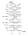
以上の構成を備えた半導体記憶装置の書き込み動作及び読み出し動作を、図5のタイミングチャートを使いながら説明する。なお、時刻TAから時刻TBまでのクロック信号CLKの1サイクルの間に書き込み動作が完了し、時刻TBから時刻TCまでのクロック信号CLKの1サイクルの間に読み出し動作が完了するものとする。 A write operation and a read operation of the semiconductor memory device having the above configuration will be described with reference to the timing chart of FIG. Note that the write operation is completed during one cycle of the clock signal CLK from time TA to time TB, and the read operation is completed during one cycle of the clock signal CLK from time TB to time TC.
まず、書き込み動作、特に、非選択メモリセル1のデータ破壊を防止することが目的のため、書き込み動作時の非選択メモリセル1、詳細には、選択された書き込み用ワード線WWLに繋がる、非選択メモリセル1、すなわち書き込み用ビット線対WBL/NWBLにデータが書き込まれないメモリセル1の書き込み動作時の制御動作に関して説明する。
First, for the purpose of preventing the data destruction of the non-selected
まず、時刻TA以前ではスタンバイ状態のため、書き込み用ビット線対WBL0/NWBL0及びWBL1/NWBL1はプリチャージ電位である電源電位(VDD電位又はHレベル)にプリチャージされている。 First, because of the standby state before time TA, the write bit line pairs WBL0 / NWBL0 and WBL1 / NWBL1 are precharged to the power supply potential (VDD potential or H level) which is a precharge potential.
次に、時刻TAで書き込み動作を示すWRITEコマンドが入力されると、メモリセル1内のデータ読み出し回路12に繋がる読み出し用ワード線RWL0が活性化される。このとき、書き込み用ビット線対WBL0/NWBL0に繋がるメモリセル1は選択されていないため、データ破壊を注意しなければならないメモリセルとなる。読み出し用ワード線RWL0の活性化によって、読み出し用ビット線RBLL0及びRBLL1にはデータが転送される。ただし、この場合、読み出し用ビット線RBLL1のデータは本発明の動作には関係がないので割愛している。非選択のメモリセル1に保持されたデータがHレベルの場合、読み出し用ビット線RBLL0にLレベルのデータが転送されローカルアンプ回路4内のAND回路31で増幅され、第1のプリチャージ電位再設定回路14にLレベル信号として転送される。次に、プリチャージ電位再設定制御信号CA0/CA1のうちCA0のみが活性化されるが第1のプリチャージ電位再設定回路14は前記Lレベル信号によって活性化されないため、第1の書き込み用ビット線WBL0はプリチャージ電位(VDDレベル又はHレベル)を保持する。この第1の書き込み用ビット線WBL0のHレベルによって第2のプリチャージ電位再設定回路15が活性化され、第2の書き込み用ビット線NWBL0をLレベルへ引き抜く。この動作により、書き込み用ビット線対WBL0/NWBL0に、非選択のメモリセル1に保持されたHレベルのデータと同じ電位関係、すなわち書き込み用ビット線対WBL0/NWBL0のうち第1の書き込み用ビット線WBL0にHレベル、第2の書き込み用ビット線NWBL0にLレベルのプリチャージ電位が再設定される。このとき、図5に示すように、第2の書き込み用ビット線NWBL0はグランド電位までプルダウンされないことが分かる。つまり、再設定されたプリチャージ電位のHレベル及びLレベルは論理値レベルで記述されるVDD電位及びグランド電位のみを言及しているわけでなく、相補の書き込み用ビット線対WBL0/NWBL0の電位レベルが一方より高い場合をHレベル、又は一方より低いレベルをLレベルという設定でよいことは言うまでもない。この機能の有効性は、メモリセル1のSNM(スタティック・ノイズ・マージン)の向上、すなわちデータ破壊防止には、ビット線対のそれぞれの電位を保持しているデータに依存した関係に電位差をつけるだけで劇的に改善することから裏付けられている。
Next, when a WRITE command indicating a write operation is input at time TA, the read word line RWL0 connected to the data read
次に、書き込み用ワード線WWL0が活性化されるが、そのタイミングは読み出し用ワード線RWL0と同じタイミングにできる。これは、非選択のメモリセル1に書き戻す動作を主眼にしているのではなく、非選択のメモリセル1の保持データと同じ電位関係に書き込み用ビット線対WBL0/NWBL0のプリチャージ電位を再設定するためである。つまり、書き込み用ビット線対WBL0/NWBL0のHレベル及びLレベルが十分電源電位及びグランド電位にならなくてもよく、よって読み出し用ワード線RWL0が活性化されてから十分の時間経過後に書き込み用ワード線WWL0を活性化させる従来の発明ほどタイミングマージンを取る必要がないためである。一方で、非選択メモリセル1のSNM不足によるデータ破壊の防止には書き込み用ビット線対WBL0/NWBL0にプリチャージ電位を再設定できてからの方がよいのは言うまでもなく、読み出し用ワード線RWL0の活性化より少し遅いタイミングで、書き込み用ワード線WWL0を活性化してもよいことは言うまでもない。また、これと同時に、選択されたメモリセル1に繋がる書き込み用ビット線対WBL1/NWBL1は通常の書き込み動作と同様、入力データDIからライトバッファ6を通じてデータが転送され、所望のメモリセル1への書き込み動作が完了する。
Next, the write word line WWL0 is activated, and the timing can be the same as that of the read word line RWL0. This does not focus on the operation of writing back to the
次に、時刻TBで読み出し動作を示すREADコマンドが入力されると、メモリセル1内のデータ読み出し回路12に繋がる読み出し用ワード線RWL0のみが活性化される。読み出し用ワード線RWL0の活性化によって、読み出し用ビット線RBLL0及びRBLL1には読み出しデータが転送される。次にローカルアンプ回路4内のデータ増幅器2がロウデコーダ9からの読み出し制御信号SE0が活性化していることを受けて、読み出し用ビット線RBLL0のデータを出力データ線GRBL0に転送し出力バッファ7によってデータ出力DOにデータDO1が出力される。同時に、読み出し用ビット線RBLL1は非選択状態のため出力データ線GRBL1に読み出されることはない。また、本動作は読み出し動作のため、プリチャージ電位再設定制御信号CA0/CA1が活性化されることもない。
Next, when a READ command indicating a read operation is input at time TB, only the read word line RWL0 connected to the data read
以上のように、書き込み動作中に非選択メモリセル1で保持しているデータを読み出して、そのデータに対応した電位関係に書き込み用ビット線対WBL/NWBLのプリチャージ電位を再設定することで、メモリセル1のSNMを飛躍的に向上させ、データ破壊を防ぐことができる。また、読み出したデータを書き戻すライトバック動作と比較しても、プリチャージ電位を再設定するだけなので読み出し用ワード線RWLの活性化と書き込み用ワード線WWLの活性化とのタイミング間隔を十分取る必要がないため書き込み動作を遅延させることなく実現できる。またメモリセル1とメモリセル1との境界領域に配置したローカルアンプ回路4内に本回路ブロックを配置し読み出し動作時に使うデータ増幅器2を使うことで、従来の一度周辺回路まで読み出してライトバックする動作と比較しても、高速にかつ小面積でプリチャージ電位再設定動作を実現できる。
As described above, the data held in the
なお、本発明では書き込み動作時に仕様上十分な書き込み時間がある場合には、プリチャージ電位再設定動作が書き込み用ビット線対WBL/NWBLへのデータ再書き込み動作、すなわち書き込み用ビット線対WBL/NWBLの電位レベルが一方はVDD電位、他方がグランド電位になるライトバック動作に等しくなることは言うまでもない。また、第2のプリチャージ電位再設定回路15のNチャネルトランジスタ36のゲート電極の制御に一方の書き込み用ビット線WBLを使用する技術によって、読み出された論理値データをデコードする、すなわち論理ゲートを付加する必要がないため、特に素子数の増加が面積オーバーヘッドの原因になるローカルアンプ回路4内等に配置することは、面積削減効果として有効である。
In the present invention, if there is a sufficient writing time in the specification during the writing operation, the precharge potential resetting operation is a data rewriting operation to the writing bit line pair WBL / NWBL, that is, the writing bit line pair WBL / Needless to say, the potential level of NWBL is equal to a write-back operation in which one is a VDD potential and the other is a ground potential. Further, the read logical value data is decoded by a technique using one write bit line WBL for controlling the gate electrode of the N-
また、ここでは本発明を分かりやすくするためにメモリセル1はデータ保持回路11とデータ読み出し回路12との合計8個のトランジスタで構成されているが、違う構成のメモリセル、例えばデータ保持回路11しかない従来の6トランジスタで構成されたメモリセルに使用してもプリチャージ電位再設定機能として有効であることは言うまでもない。あわせてデータ増幅器2で使われているシングルエンドアンプに代えて差動アンプを使ってもよいことは言うまでもない。
Here, in order to make the present invention easier to understand, the
また、第1のプリチャージ電位再設定回路14内のNチャネルトランジスタ34のサイズ、例えばチャネル長が、第2のプリチャージ電位再設定回路15内のNチャネルトランジスタ36のサイズ、例えばチャネル長より大きいことを特徴とする。すなわち、第1のプリチャージ電位再設定回路14のトランジスタ能力が、第2のプリチャージ電位再設定回路15のトランジスタ能力より大きいことを特徴とする。
Further, the size of the
このように、一方のプルダウントランジスタ34のトランジスタサイズが、他方のプルダウントランジスタ36のトランジスタサイズより大きい、つまり直接読み出しデータの信号によって活性化される第1のプリチャージ電位再設定回路14のトランジスタ能力を大きくすることで、データ増幅器2のデータがHデータ(VDD電位又は電源電位)の場合に、書き込み用ビット線対WBL/NWBLのプリチャージ電位がHレベル(VDD電位)のためプリチャージ電位再設定制御信号CAが活性化されると、第2の書き込み用ビット線NWBLをLレベルに引き抜く以前に第1の書き込み用ビット線WBLをLレベルに引き抜くことができる。これによって、第2のプリチャージ電位再設定回路15内のゲート電極が第1の書き込み用ビット線WBLに繋がるNチャネルトランジスタ36を非活性状態にすることができ、誤ったプリチャージ電位を再設定することはない。
In this way, the transistor size of the first pull-
なお、第1のプリチャージ電位再設定回路14のトランジスタ能力を第2のプリチャージ電位再設定回路15より大きくすることとしたが、第2のプリチャージ電位再設定回路15のトランジスタサイズを十分小さくする、例えばチャネル長を小さく、もしくはチャネル幅を太くすることでも、所定時間内にプリチャージ電位を再設定できる能力があれば十分であることは言うまでもない。
Although the transistor capability of the first precharge
また、図3に示したように、第1及び第2のプリチャージ電位再設定回路14,15内のNチャネルプルダウントランジスタ34,36と書き込み用ビット線対WBL/NWBLとの間に直列に接続されたNチャネルトランジスタ35,37とを備え、Nチャネルトランジスタ35,37のゲート電極は書き込み用制御回路の出力信号、すなわちプリチャージ電位再設定制御信号CAに接続されていることを特徴とする。これによって、第2の書き込み用ビット線NWBLをプリチャージするたびに、当該第2の書き込み用ビット線NWBLが勝手にプルダウン動作する誤動作を防ぐことができる。
As shown in FIG. 3, the N-channel pull-down
なお、第1及び第2のプリチャージ電位再設定回路14,15にはプリチャージ電位再設定制御信号CAで制御するNチャネルトランジスタ35,37を備えているが、それぞれのNチャネルトランジスタ35,37のゲート電極をプリチャージ電位再設定制御信号CAの論理を加味した制御信号に変えることで、直列に2段ならんだNチャネルトランジスタを1段にすることができるのは言うまでもない。又は、書き込み用ビット線対WBL/NWBLをHレベル(VDD電位又は電源電位)のプリチャージではなく、Lレベル(グランド電位又はVSS電位)のプリチャージとして、非選択メモリセル1に繋がる書き込み用ビット線対WBL/NWBLのみプリチャージ電位再設定制御信号CAの活性化後にHレベルへプリチャージする書き込み用ビット線対WBL/NWBLのプリチャージデコード方式でも直列に2段ならんだNチャネルトランジスタを1段にすることができるのは言うまでもない。なお、書き込み用ビット線対WBL/NWBLのプリチャージ電位がHレベルの場合に言及しているため、第1及び第2のプリチャージ電位再設定回路14,15はNチャネルトランジスタ34〜37で構成されているが、書き込み用ビット線対WBL/NWBLのプリチャージ電位がLレベル(グランド電位又はVSS電位)の場合にはPチャネルトランジスタで構成すればよいことは言うまでもない。
The first and second precharge
また、書き込み用制御回路の出力信号すなわちプリチャージ電位再設定制御信号CAはメモリセル1で配置された読み出し用ワード線RWL及び書き込み用ワード線WWLと同じ方向に配置されていることを特徴とする。これによって、特にローカルアンプ回路4を持つ場合は、ビット線方向に制御信号を配置するより効率的に配置できるため面積オーバーヘッドの削減として有効である。
Further, the output signal of the write control circuit, that is, the precharge potential reset control signal CA is arranged in the same direction as the read word line RWL and the write word line WWL arranged in the
また、第1及び第2のプリチャージ電位再設定回路14,15内の直列に接続されたNチャネルトランジスタ35,37とNチャネルプルダウントランジスタ34,36とのトランジスタサイズが同じであることを特徴とする。これによって、プルダウン能力を一定にできるためトランジスタばらつき等の影響を受けにくいメリットがある。
The N-
また、第1及び第2のプリチャージ電位再設定回路14,15のNチャネルプルダウントランジスタ34,36のトランジスタサイズ、すなわちトランジスタ能力は、書き込み用ビット線対WBL/NWBLに繋がったライトバッファ6のバッファサイズより小さいことを特徴とする。書き込み用ビット線対WBL/NWBLのプリチャージを再設定する能力があればよい第1及び第2のプリチャージ電位再設定回路14,15のトランジスタ能力を十分小さくすることで、ローカルアンプ回路4内の面積オーバーヘッドを小さくすることができる。
The transistor size of the N-channel pull-down
また、書き込み用ビット線対WBL/NWBLに2つのPチャネルトランジスタ41,42からなる図4のキーパー回路5を備えることを特徴とする。これによって、プルダウン機能しかない第1及び第2のプリチャージ電位再設定回路14,15で誤動作、すなわちHデータ(VDD電位又は電源電位)がLデータへ変化した場合に、一方のプルアップPチャネルトランジスタ41又は42でHデータへプルアップできる。また、ライトバッファ6がNチャネルトランジスタのみで構成されている、すなわちプルダウン機能しかない場合は、ライト動作を補助する機能としても併用できるため、動作の安定性と面積オーバーヘッドの削減を実現できる。
Further, the write bit line pair WBL / NWBL includes the
また、プルダウントランジスタ34,36及びNチャネルトランジスタ35,37を含む制御回路、すなわち第1及び第2のプリチャージ電位再設定回路14,15が、データ増幅器2と同じ領域に配置され、かつ当該領域はメモリアレイ内に1つ以上存在する、メモリセル1とメモリセル1との間の境界領域であることを特徴とする。すなわち、ローカルアンプ回路4内のように、メモリセルアレイとメモリセルアレイとの境界に配置することで、本発明の対象となる非選択メモリセル1からの物理距離が周辺回路に配置されたライトバック回路と比較して短くなり、より高速にプリチャージ電位再設定動作を書き込み用ビット線対WBL/NWBLに実現できる。なお、ローカルアンプ回路4がI/F回路8にしか配置していない場合にも本発明はライトバック動作に比べて有効であることは言うまでもない。
A control circuit including pull-down
また、ロウデコーダ9からの書き込み用制御回路の出力信号は、書き込み動作をマスクされた書き込み用ビット線対WBL/NWBLを示すアドレス信号を活性化することを特徴とする。すなわち、図5で示す書き込み用ビット線対WBL1/NWBL1に繋がった選択メモリセル1へのライト動作にマスク機能が付加された場合、すなわち選択的に書き込みをマスクする場合に、対象アドレス、つまりプリチャージ電位再設定制御信号CA1が活性化されて書き込み用ビット線対WBL1/NWBL1のプリチャージを再設定する機能を有する。これによって、書き込み時にマスクされたことによって非選択となったメモリセル1のSNMの向上を実現することができる。
The output signal of the write control circuit from the
《実施形態1の第1変形例》
本発明の実施形態1の第1変形例は、基本的な形態及び効果が実施形態1と同じである。以下、実施形態1の第1変形例に関して図6の回路図を用いながら説明する。図6で示す半導体記憶装置は、図3で示す回路図に対して、Nチャネルトランジスタ35,37を削除し、Nチャンネルプルダウントランジスタ34,36の各々のソース電位をVSS電位(又は接地電位)から信号線NCAに変更した回路である。つまり、第1及び第2のプリチャージ電位再設定回路14,15がそれぞれ1段のNチャネルトランジスタ34,36で構成される。なお、図6でも、図3と同様に信号線及び信号における末尾の「0」又は「1」を省略している。<< First Modification of
The first modification of the first embodiment of the present invention has the same basic form and effect as the first embodiment. Hereinafter, a first modification of the first embodiment will be described with reference to the circuit diagram of FIG. The semiconductor memory device shown in FIG. 6 is different from the circuit diagram shown in FIG. 3 in that the N-
以上の構成を備えた半導体記憶装置の書き込み動作時の選択動作に関して、図7のタイミングチャートは、図5のタイミングチャート中のプリチャージ電位再設定制御信号CAの論理値が反転して信号NCAになったものである。 Regarding the selection operation at the time of the write operation of the semiconductor memory device having the above configuration, the timing chart of FIG. 7 inverts the logic value of the precharge potential reset control signal CA in the timing chart of FIG. It has become.
以上のように、Nチャネルトランジスタ35,37を削除し、Nチャンネルプルダウントランジスタ34,36のソース電位をVSS電位(又は接地電位)から信号線NCAに変更することで、上記実施形態1の効果に加えて、ローカルアンプ回路4内のトランジスタ数を削減できることで面積削減に有効である。
As described above, by removing the N-
また、信号線NCAの制御回路をロウデコーダ9内に配置することで、もともとローカルアンプ回路4に対応したデッドスペースとなるロウデコーダ9内の領域を有効利用できるため、面積の大きなオーバーヘッドなしに容易に回路動作を実現できて有効である。
In addition, by arranging the control circuit for the signal line NCA in the
なお、信号NCAの制御回路はロウデコーダ9内に配置するとしているが、I/F回路8内に配置してもよいことは言うまでもない。
Although the control circuit for the signal NCA is arranged in the
《実施形態1の第2変形例》
本発明の実施形態1の第2変形例は、基本的な形態及び効果が実施形態1と同じである。以下、実施形態1の第2変形例に関して図8のブロック図を用いながら説明する。図8で示す半導体記憶装置は、図1で示す半導体記憶装置のライトバッファ6がライトバック機能付ライトバッファ6aに置き換えられ、出力バッファ7からデータ出力信号DOに相当するライトバックデータWBがライトバッファ6aに入力される構成となっている。なお、図8でも、図2〜4及び図6と同様に信号線及び信号における末尾の「0」又は「1」を省略している。<< Second Modification of
The second modification of the first embodiment of the present invention has the same basic form and effect as the first embodiment. Hereinafter, a second modification of the first embodiment will be described with reference to the block diagram of FIG. In the semiconductor memory device shown in FIG. 8, the
以上の構成を備えた半導体記憶装置の書き込み動作時の、主として非選択メモリセル1の制御動作に関して、図9を用いて説明する。まず、時刻TAでWRITEコマンドが入力されると、読み出し用ワード線RWL0が活性化され、非選択メモリセル1の保持データが読み出され、そのデータに対応した電位関係に書き込み用ビット線対WBL0/NWBL0のプリチャージ電位が再設定される。この動作は、図3にて説明したものと同様である。
The control operation of the
次に、書き込み用ワード線WWL0が活性化されると、データ増幅器2は読み出し制御信号SE0が活性化されているため出力データ線GRBL0に非選択メモリセル1のデータを転送する。この信号を出力バッファ7で増幅したライトバックデータWBを使ってライトバッファ6aによりデータを書き込む、すなわちライトバック動作が実施される。また、これと同時に、選択されたメモリセル1に繋がる書き込み用ビット線対WBL1/NWBL1は通常の書き込み動作と同様、入力データDIからライトバッファ6aを通じてデータが転送され、所望のメモリセル1への書き込み動作が完了する。
Next, when the write word line WWL0 is activated, the
以上のように、書き込み動作中に非選択メモリセル1で保持しているデータを読み出して、そのデータに対応した電位関係に書き込み用ビット線対WBL/NWBLのプリチャージ電位を再設定し、その後ライトバッファ6aを使ってデータをライトバックすることで、メモリセル1のSNMを飛躍的に向上させ、データ破壊を防ぐことができる。また、読み出したデータを書き戻すライトバック動作しか持たない半導体記憶装置と比較しても、選択ワード線が活性化された直後にプリチャージ電位を再設定することで、ワード線活性化直後のSNM不良を改善できるとともに、その後ライトバックすることで確実にデータリストアを実現できるため、SNMの向上には有効である。
As described above, the data held in the
なお、プリチャージ電位再設定回路3内のNチャネルプルダウントランジスタ34,36のサイズは、ライトバッファ6a内のNチャネルトランジスタのサイズより小さい、すなわちトランジスタ能力が小さいことを特徴とする。このように、ライトバッファ6a内のNチャネルトランジスタのサイズよりプリチャージ電位再設定回路3内のNチャネルプルダウントランジスタ34,36のサイズを小さくすることで、選択メモリセル1に場所として近い、すなわち配線負荷が軽く見えるプリチャージ電位再設定回路3内のNチャネルプルダウントランジスタ34,36によるドライブ能力を抑え、以てデータリストアの誤動作を防ぐとともに、ローカルアンプ回路4を小さくできるため省面積化に有効である。
The size of the N-channel pull-down
また、プリチャージ電位再設定回路3内のNチャネルプルダウントランジスタ34,36の一方が活性化した後にライトバッファ6a内のNチャネルトランジスタを活性化する、すなわちドライブ能力の小さなドライバで一定の電位レベルまで書き戻した後、ドライブ能力の大きなドライバで一気に書き戻すことで、データリストア動作の誤動作やピーク電流を抑制することができる。
Further, after one of the N-channel pull-down
《実施形態2》
本発明の実施形態2の半導体記憶装置を、図10のブロック図を用いながら説明する。図10に示す半導体記憶装置は、図1で示すブロック図に対して、書き込み用ビット線対WBL0/NWBL0及びWBL1/NWBL1に、NチャネルトランスファーゲートN0,N1,N2,N3,N4,N5,N6,N7,N8,N9,N10,N11,N12,N13,N14及びN15が付加され、書き込み制御用選択信号SEL0,SEL1,SEL2,SEL3,SEL4,SEL5,SEL6及びSEL7でスイッチ動作を制御する機能を備える。<<
A semiconductor memory device according to
以上の構成を備えた半導体記憶装置の書き込み動作時の選択動作に関して、図11のタイミングチャートを使いながら説明する。なお、時刻TAから時刻TBまでのクロック信号CLKの1サイクルの間に書き込み動作が完了するものとする。 A selection operation during a write operation of the semiconductor memory device having the above configuration will be described with reference to the timing chart of FIG. Note that the write operation is completed in one cycle of the clock signal CLK from time TA to time TB.
時刻TAでWRITEコマンドの入力により書き込み動作が開始され、選択されたアドレスに対応する書き込み用ワード線WWL1及び読み出し用ワード線RWL1が活性化される。また、書き込まれるメモリセル1はセル#5であるためにセル#1が非選択メモリセルとなり、本発明の実施形態1のプリチャージ電位再設定動作が行われる。このとき、NチャネルトランスファーゲートN0〜N7に繋がる選択信号SEL0〜SEL3は、非選択となった書き込み用ビット線対WBL0/NWBL0と同じアドレスでかつ選択されたメモリセル1を含むメモリセルアレイの境界領域にある出力信号のみ活性化する、すなわち書き込み制御用選択信号SEL1のみが活性化のままで、他の書き込み制御用選択信号SEL0,SEL2,SEL3は非活性状態になる。また選択されたセル#5に繋がる書き込み用ビット線対WBL1/NWBL1は入力データをセル#5に転送する必要があるために、書き込み用ビット線対WBL1/NWBL1に繋がる全てのNチャネルトランスファーゲートN8〜N15を制御する書き込み制御用選択信号SEL4,SEL5,SEL6及びSEL7は活性化状態を維持し、書き込み動作が行われる。
At time TA, a write operation is started by inputting a WRITE command, and the write word line WWL1 and the read word line RWL1 corresponding to the selected address are activated. Further, since the
以上のように、書き込み制御用選択信号SEL0〜SEL3のうちSEL1のみが活性化されることによってセル#1に繋がる書き込み用ビット線対WBL0/NWBL0の配線負荷が通常の場合と比べて小さくできるため、メモリセル1のデータ保持性能を阻害する外部からの負荷ノイズを軽減することができ、メモリセル1のSNM向上には有効である。また、書き込み用ビット線対WBL0/NWBL0の配線負荷が小さいことは、プリチャージ電位再設定動作に使われる第1及び第2のプリチャージ電位再設定回路14,15のトランジスタ能力を抑制しても高速にプリチャージ電位再設定動作を実現できるため、高速かつ小面積な半導体記憶装置を実現することができる。
As described above, since only SEL1 of the write control selection signals SEL0 to SEL3 is activated, the wiring load of the write bit line pair WBL0 / NWBL0 connected to the
なお、書き込み用ビット線対WBL0/NWBL0に繋がるNチャネルトランスファーゲートN2及びN3のみの活性化を維持する制御の一例を示したが、例えば、NチャネルトランスファーゲートN4及びN5も活性化を維持する、すなわち前例より配線負荷が若干増えるが配線制御の複雑性を削減することで回路面積を削減する手段でもよいことは言うまでもない。 Although an example of the control for maintaining the activation of only the N-channel transfer gates N2 and N3 connected to the write bit line pair WBL0 / NWBL0 has been shown, for example, the N-channel transfer gates N4 and N5 also maintain the activation. That is, although the wiring load is slightly increased as compared with the previous example, it is needless to say that means for reducing the circuit area by reducing the complexity of wiring control may be used.
また、書き込み用ビット線対WBL1/NWBL1に配置されたNチャネルトランスファーゲートN8〜N15は活性化状態を維持する制御をしているが、書き込み用ビット線対WBL0/NWB0に繋がるNチャネルトランスファーゲートN0〜N7と同じ制御にして、書き込み動作をローカルアンプ回路4に配置されたライトバッファもしくは第1及び第2のプリチャージ電位再設定回路14,15を使って書き込む機能を備えることで、書き込み動作時の配線負荷を軽減でき、かつI/F回路8からの書き込み動作時に負荷となるNチャネルトランスファーゲートN0〜N15の影響を削減できるために高速書き込み動作を実現できることは言うまでもない。特に、第1及び第2のプリチャージ電位再設定回路14,15をライトバッファとして併用する制御を持つことは、I/F回路8内のライトバッファ6を削減できるので面積削減に有効である。
The N channel transfer gates N8 to N15 arranged in the write bit line pair WBL1 / NWBL1 are controlled to maintain the activated state, but the N channel transfer gate N0 connected to the write bit line pair WBL0 / NWB0. To the same control as N7, and the write operation is provided by using the write buffer arranged in the
なお、本実施形態と上記実施形態1又はその変形例とを組み合わせることで、より一層の効果を期待できることは言うまでもない。 Needless to say, a further effect can be expected by combining the present embodiment with the first embodiment or its modification.
本発明に係る半導体記憶装置は、特に微細化されたメモリセルを安定的に動作させかつ高速動作を実現する技術を有し、多数かつ多種類の仕様のメモリを搭載するシステムLSI等に有用である。 The semiconductor memory device according to the present invention is particularly useful for a system LSI or the like that has a technology for stably operating a miniaturized memory cell and realizing a high-speed operation, and mounting a large number of various types of memories. is there.
1 メモリセル
2 データ増幅器
3 プリチャージ電位再設定回路
4 ローカルアンプ回路
5 キーパー回路
6 ライトバッファ
6a ライトバック機能付ライトバッファ
7 出力バッファ
8 I/F回路
9 ロウデコーダ
10 制御回路
11 データ保持回路
12 データ読み出し回路
13 データ転送制御回路
14,15 第1及び第2のプリチャージ電位再設定回路1
Claims (17)
前記読み出し用ビット線に繋がったデータ増幅器と、
前記書き込み用ビット線対に各々繋がったプルダウントランジスタとを備え、
前記データ増幅器の出力が一方の前記プルダウントランジスタのゲート電極に接続されて、他方の前記プルダウントランジスタのゲート電極に前記書き込み用ビット線対の一方が接続されていることを特徴とする半導体記憶装置。 A circuit including a data holding circuit configured to store data by the first and second circuit elements, and a transistor arranged to connect the data holding circuit to the read bit line and the write bit line pair A memory cell composed of
A data amplifier connected to the read bit line;
A pull-down transistor connected to each of the write bit line pairs,
An output of the data amplifier is connected to a gate electrode of one of the pull-down transistors, and one of the write bit line pairs is connected to a gate electrode of the other pull-down transistor.
前記データ増幅器の出力が接続されるプルダウントランジスタのトランジスタサイズは、前記書き込み用ビット線対の一方に接続されているプルダウントランジスタのトランジスタサイズより大きいことを特徴とする半導体記憶装置。 The semiconductor memory device according to claim 1.
2. A semiconductor memory device according to claim 1, wherein a transistor size of a pull-down transistor connected to the output of the data amplifier is larger than a transistor size of a pull-down transistor connected to one of the pair of write bit lines.
前記それぞれのプルダウントランジスタと前記書き込み用ビット線対との間に直列に接続されたNチャネルトランジスタを更に備え、
前記Nチャネルトランジスタのゲート電極は書き込み用制御回路の出力信号に接続されていることを特徴とする半導体記憶装置。 The semiconductor memory device according to claim 2.
An N-channel transistor connected in series between each of the pull-down transistors and the write bit line pair;
A semiconductor memory device, wherein a gate electrode of the N-channel transistor is connected to an output signal of a write control circuit.
前記それぞれのプルダウントランジスタのソース線が電源線以外の信号線に接続されていることを特徴とする半導体記憶装置。 The semiconductor memory device according to claim 2.
A semiconductor memory device, wherein the source line of each pull-down transistor is connected to a signal line other than a power supply line.
前記信号線は、ロウデコーダ内に配置された制御回路からの信号線であることを特徴とする半導体記憶装置。 The semiconductor memory device according to claim 4.
The semiconductor memory device, wherein the signal line is a signal line from a control circuit disposed in a row decoder.
前記書き込み用制御回路の出力信号は、前記メモリセルで配置された読み出し用及び書き込み用ワード線と同じ方向に配置されていることを特徴とする半導体記憶装置。 The semiconductor memory device according to claim 3.
An output signal of the write control circuit is arranged in the same direction as the read and write word lines arranged in the memory cell.
前記書き込み用制御回路の出力信号は、書き込み時に非選択となった書き込み用ビット線対と同じアドレスを選択する信号のみ活性化することを特徴とする半導体記憶装置。 The semiconductor memory device according to claim 3.
An output signal of the write control circuit activates only a signal for selecting the same address as a write bit line pair that is not selected at the time of writing.
前記直列に接続されたNチャネルトランジスタとプルダウントランジスタとのトランジスタサイズが同じであることを特徴とする半導体記憶装置。 The semiconductor memory device according to claim 3.
A semiconductor memory device, wherein the N-channel transistor and the pull-down transistor connected in series have the same transistor size.
前記プルダウントランジスタのトランジスタサイズは、前記書き込み用ビット線対に繋がったライトバッファのバッファサイズより小さいことを特徴とする半導体記憶装置。 The semiconductor memory device according to claim 2.
A semiconductor memory device, wherein a transistor size of the pull-down transistor is smaller than a buffer size of a write buffer connected to the write bit line pair.
前記書き込み用ビット線対に2つのPチャネルトランジスタが、ゲート電極は前記書き込み用ビット線対の一方に、ソースは電源電圧に、ドレインは前記書き込み用ビット線対の他方にそれぞれ繋がっていることを特徴とする半導体記憶装置。 The semiconductor memory device according to claim 2.
Two P-channel transistors are connected to the write bit line pair, a gate electrode is connected to one of the write bit line pair, a source is connected to a power supply voltage, and a drain is connected to the other of the write bit line pair. A semiconductor memory device.
入力データを前記書き込み用ビット線対に転送するライトバッファ機能と、前記データ増幅器の出力を前記書き込み用ビット線対に転送するライトバック機能とを有するライトバッファを更に備えたことを特徴とする半導体記憶装置。 The semiconductor memory device according to claim 1.
A semiconductor further comprising a write buffer function having a write buffer function for transferring input data to the write bit line pair and a write back function for transferring an output of the data amplifier to the write bit line pair. Storage device.
前記プルダウントランジスタのサイズは、前記ライトバッファを構成するNチャンネルトランジスタのサイズより小さいことを特徴とする半導体記憶装置。 The semiconductor memory device according to claim 11.
2. The semiconductor memory device according to claim 1, wherein a size of the pull-down transistor is smaller than a size of an N channel transistor constituting the write buffer.
前記ライトバック機能は、前記プルダウントランジスタの一方が活性化された後に活性化されることを特徴とする半導体記憶装置。 The semiconductor memory device according to claim 11.
The write-back function is activated after one of the pull-down transistors is activated.
前記プルダウントランジスタ及び前記Nチャネルトランジスタを含む制御回路が、前記データ増幅器と同じ領域に配置され、かつ前記領域はメモリアレイ内に1つ以上存在するメモリアレイとメモリアレイとの間の境界領域であることを特徴とする半導体記憶装置。 The semiconductor memory device according to claim 3.
A control circuit including the pull-down transistor and the N-channel transistor is disposed in the same region as the data amplifier, and the region is a boundary region between the memory array and one or more memory arrays existing in the memory array. A semiconductor memory device.
前記境界領域上で前記メモリアレイとメモリアレイを接続するように配置されたNチャネルトランスファーゲートを更に備え、
前記Nチャネルトランスファゲートのゲート電極が前記書き込み用制御回路からの選択信号に接続されていることを特徴とする半導体記憶装置。 The semiconductor memory device according to claim 14.
An N-channel transfer gate disposed on the boundary region to connect the memory array and the memory array;
A semiconductor memory device, wherein a gate electrode of the N-channel transfer gate is connected to a selection signal from the write control circuit.
前記Nチャネルトランスファーゲートに繋がる出力信号は、非選択となった書き込み用ビット線対と同じアドレスでかつ選択されたメモリセルを含む前記メモリセルアレイの境界領域にある出力信号のみ活性化することを特徴とする半導体記憶装置。 The semiconductor memory device according to claim 15.
The output signal connected to the N-channel transfer gate is activated only for the output signal in the boundary area of the memory cell array having the same address as the non-selected write bit line pair and including the selected memory cell. A semiconductor memory device.
前記書き込み用制御回路の出力信号は、書き込み動作をマスクされた書き込み用ビット線対を示すアドレス信号を活性化することを特徴とする半導体記憶装置。 The semiconductor memory device according to claim 3.
An output signal of the write control circuit activates an address signal indicating a write bit line pair masked for a write operation.
Priority Applications (1)
| Application Number | Priority Date | Filing Date | Title |
|---|---|---|---|
| JP2012536153A JP5763659B2 (en) | 2010-10-01 | 2011-07-26 | Semiconductor memory device |
Applications Claiming Priority (6)
| Application Number | Priority Date | Filing Date | Title |
|---|---|---|---|
| JP2010223964 | 2010-10-01 | ||
| JP2010223964 | 2010-10-01 | ||
| JP2011003176 | 2011-01-11 | ||
| JP2011003176 | 2011-01-11 | ||
| JP2012536153A JP5763659B2 (en) | 2010-10-01 | 2011-07-26 | Semiconductor memory device |
| PCT/JP2011/004216 WO2012042723A1 (en) | 2010-10-01 | 2011-07-26 | Semiconductor memory device |
Publications (2)
| Publication Number | Publication Date |
|---|---|
| JPWO2012042723A1 JPWO2012042723A1 (en) | 2014-02-03 |
| JP5763659B2 true JP5763659B2 (en) | 2015-08-12 |
Family
ID=45892221
Family Applications (1)
| Application Number | Title | Priority Date | Filing Date |
|---|---|---|---|
| JP2012536153A Expired - Fee Related JP5763659B2 (en) | 2010-10-01 | 2011-07-26 | Semiconductor memory device |
Country Status (4)
| Country | Link |
|---|---|
| US (1) | US8755217B2 (en) |
| JP (1) | JP5763659B2 (en) |
| CN (1) | CN102934169B (en) |
| WO (1) | WO2012042723A1 (en) |
Families Citing this family (4)
| Publication number | Priority date | Publication date | Assignee | Title |
|---|---|---|---|---|
| US9053817B2 (en) | 2013-03-15 | 2015-06-09 | Taiwan Semiconductor Manufacturing Company, Ltd. | Amplifier |
| US10607692B2 (en) * | 2017-06-29 | 2020-03-31 | SK Hynix Inc. | Serializer and memory device including the same |
| US11670349B2 (en) * | 2021-03-31 | 2023-06-06 | Changxin Memory Technologies, Inc. | Memory circuit, memory precharge control method and device |
| CN117476067A (en) * | 2023-11-01 | 2024-01-30 | 合芯科技(苏州)有限公司 | Pull-down circuit, memory and data writing method |
Citations (6)
| Publication number | Priority date | Publication date | Assignee | Title |
|---|---|---|---|---|
| JP2004071106A (en) * | 2002-08-08 | 2004-03-04 | Renesas Technology Corp | Semiconductor memory device |
| JP2005275382A (en) * | 2004-02-25 | 2005-10-06 | Hitachi Displays Ltd | Display device |
| JP2007004888A (en) * | 2005-06-23 | 2007-01-11 | Toshiba Corp | Semiconductor memory device and its control method |
| WO2008032549A1 (en) * | 2006-09-13 | 2008-03-20 | Nec Corporation | Semiconductor storage device |
| JP2008198242A (en) * | 2007-02-08 | 2008-08-28 | Toshiba Corp | Semiconductor memory device |
| JP2009163787A (en) * | 2007-12-28 | 2009-07-23 | Toshiba Corp | Semiconductor memory device |
Family Cites Families (3)
| Publication number | Priority date | Publication date | Assignee | Title |
|---|---|---|---|---|
| US7969400B2 (en) | 2004-02-25 | 2011-06-28 | Hitachi Displays, Ltd. | Liquid crystal display device with decreased power consumption |
| US20090161410A1 (en) * | 2007-12-21 | 2009-06-25 | Texas Instruments Inc. | Seven transistor sram cell |
| US8654575B2 (en) * | 2010-07-16 | 2014-02-18 | Texas Instruments Incorporated | Disturb-free static random access memory cell |
-
2011
- 2011-07-26 JP JP2012536153A patent/JP5763659B2/en not_active Expired - Fee Related
- 2011-07-26 CN CN201180021805.9A patent/CN102934169B/en not_active Expired - Fee Related
- 2011-07-26 WO PCT/JP2011/004216 patent/WO2012042723A1/en active Application Filing
-
2012
- 2012-10-19 US US13/656,320 patent/US8755217B2/en not_active Expired - Fee Related
Patent Citations (6)
| Publication number | Priority date | Publication date | Assignee | Title |
|---|---|---|---|---|
| JP2004071106A (en) * | 2002-08-08 | 2004-03-04 | Renesas Technology Corp | Semiconductor memory device |
| JP2005275382A (en) * | 2004-02-25 | 2005-10-06 | Hitachi Displays Ltd | Display device |
| JP2007004888A (en) * | 2005-06-23 | 2007-01-11 | Toshiba Corp | Semiconductor memory device and its control method |
| WO2008032549A1 (en) * | 2006-09-13 | 2008-03-20 | Nec Corporation | Semiconductor storage device |
| JP2008198242A (en) * | 2007-02-08 | 2008-08-28 | Toshiba Corp | Semiconductor memory device |
| JP2009163787A (en) * | 2007-12-28 | 2009-07-23 | Toshiba Corp | Semiconductor memory device |
Also Published As
| Publication number | Publication date |
|---|---|
| JPWO2012042723A1 (en) | 2014-02-03 |
| US8755217B2 (en) | 2014-06-17 |
| CN102934169B (en) | 2015-09-30 |
| US20130044551A1 (en) | 2013-02-21 |
| WO2012042723A1 (en) | 2012-04-05 |
| CN102934169A (en) | 2013-02-13 |
Similar Documents
| Publication | Publication Date | Title |
|---|---|---|
| US9214222B2 (en) | Semiconductor device having timing control for read-write memory access operations | |
| US7259986B2 (en) | Circuits and methods for providing low voltage, high performance register files | |
| JP4285511B2 (en) | Semiconductor memory device | |
| EP3054452A1 (en) | Methods and apparatus for reducing power consumption in memory circuitry by controlling precharge duration | |
| US8000130B2 (en) | Semiconductor memory device with sense circuit connected to sense node coupled to bit line | |
| JP4005535B2 (en) | Semiconductor memory device | |
| JP2009505315A (en) | SRAM cell having independent read / write circuit | |
| JP5798120B2 (en) | Semiconductor memory device | |
| US7345936B2 (en) | Data storage circuit | |
| JPH10208484A (en) | Semiconductor memory and data read circuit therefor | |
| US7535753B2 (en) | Semiconductor memory device | |
| US6339541B1 (en) | Architecture for high speed memory circuit having a relatively large number of internal data lines | |
| WO2015001722A1 (en) | Semiconductor storage device | |
| WO2006073060A1 (en) | Semiconductor storage device | |
| JP5763659B2 (en) | Semiconductor memory device | |
| JP2009070474A (en) | Semiconductor integrated circuit | |
| JP4954954B2 (en) | Semiconductor memory device | |
| US20110305073A1 (en) | Semiconductor memory device | |
| US20100315890A1 (en) | Memory array with corresponding row and column control signals | |
| US7345927B2 (en) | Semiconductor integrated circuit device | |
| TWI484499B (en) | Ripple bit-lines/search-lines for improving leakage/variation tolerance and density/performance of static random access memory | |
| JPS6258075B2 (en) |
Legal Events
| Date | Code | Title | Description |
|---|---|---|---|
| A621 | Written request for application examination |
Free format text: JAPANESE INTERMEDIATE CODE: A621 Effective date: 20140509 |
|
| A131 | Notification of reasons for refusal |
Free format text: JAPANESE INTERMEDIATE CODE: A131 Effective date: 20150317 |
|
| A711 | Notification of change in applicant |
Free format text: JAPANESE INTERMEDIATE CODE: A712 Effective date: 20150414 |
|
| A521 | Request for written amendment filed |
Free format text: JAPANESE INTERMEDIATE CODE: A523 Effective date: 20150420 |
|
| TRDD | Decision of grant or rejection written | ||
| A01 | Written decision to grant a patent or to grant a registration (utility model) |
Free format text: JAPANESE INTERMEDIATE CODE: A01 Effective date: 20150602 |
|
| A61 | First payment of annual fees (during grant procedure) |
Free format text: JAPANESE INTERMEDIATE CODE: A61 Effective date: 20150611 |
|
| R150 | Certificate of patent or registration of utility model |
Ref document number: 5763659 Country of ref document: JP Free format text: JAPANESE INTERMEDIATE CODE: R150 |
|
| LAPS | Cancellation because of no payment of annual fees |