JP2004126658A - Processor system - Google Patents
Processor system Download PDFInfo
- Publication number
- JP2004126658A JP2004126658A JP2002285740A JP2002285740A JP2004126658A JP 2004126658 A JP2004126658 A JP 2004126658A JP 2002285740 A JP2002285740 A JP 2002285740A JP 2002285740 A JP2002285740 A JP 2002285740A JP 2004126658 A JP2004126658 A JP 2004126658A
- Authority
- JP
- Japan
- Prior art keywords
- program
- address
- storage unit
- processor system
- rom
- Prior art date
- Legal status (The legal status is an assumption and is not a legal conclusion. Google has not performed a legal analysis and makes no representation as to the accuracy of the status listed.)
- Abandoned
Links
Images


Classifications
-
- G—PHYSICS
- G06—COMPUTING; CALCULATING OR COUNTING
- G06F—ELECTRIC DIGITAL DATA PROCESSING
- G06F11/00—Error detection; Error correction; Monitoring
- G06F11/36—Preventing errors by testing or debugging software
- G06F11/362—Software debugging
- G06F11/3648—Software debugging using additional hardware
Landscapes
- Engineering & Computer Science (AREA)
- Computer Hardware Design (AREA)
- Theoretical Computer Science (AREA)
- Quality & Reliability (AREA)
- Physics & Mathematics (AREA)
- General Engineering & Computer Science (AREA)
- General Physics & Mathematics (AREA)
- Debugging And Monitoring (AREA)
- Stored Programmes (AREA)
- Hardware Redundancy (AREA)
Abstract
Description
【0001】
【発明の属する技術分野】
本発明は、第1のプログラム記憶部に記憶された第1のプログラムの少なくとも一部を更新したり、デバックすることが可能なプロセッサシステムに関する。
【0002】
【従来の技術】
ワンチップマイクロコンピュータ(以下、ワンチップマイコン)は、内部にマスクROMを備えていることが多い。この種のマスクROMには、製造時に予めマイクロコードが組み込まれているが、マスクROMはデータの書き換えができないため、マイクロコードに誤りがあると、そのマイコン自体を交換しなければならず、保守性が悪く、故障時のコストがかかってしまう。
【0003】
このような問題を解消するため、プログラムROM内のマイクロコードに誤りがあったときに、その誤りのある箇所だけを更新できるようにしたプロセッサシステムが実用化されている。
【0004】
図3はこの種の従来のプロセッサシステムの概略構成を示すブロック図である。図3のプロセッサシステムは、プログラムROM1と、インストラクションデコーダ2と、プログラムRAM3と、ROMアドレスレジスタ4と、プログラムカウンタ5と、強制分岐先PCレジスタ6と、アドレス比較部7と、セレクタ8と、書き込み回路12とを備えている。
【0005】
プログラムRAM3には、誤りを直した正しいマイクロコードが格納される。ROMアドレスレジスタ4は、プログラムROM1に格納されているマイクロコード中の誤りのある箇所(アドレス)を記憶する。強制分岐先PCレジスタ6は、プログラムRAM3中の実行すべきアドレスを記憶する。ROMアドレスレジスタ4と強制分岐先PCレジスタ6には、書き込み回路12が各アドレスを記憶する。
【0006】
アドレス比較部7は、プログラムカウンタ5がROMアドレスレジスタ4に記憶されたアドレスに一致したか否かを判断する。セレクタ8は、プログラムカウンタ5がROMアドレスレジスタ4に記憶されたアドレスに一致すると、プログラムカウンタ5を強制分岐先PCレジスタ6に記憶されているアドレスに置き換える。
【0007】
例えば、プログラムROM1に格納されているマイクロコードの特定箇所に誤りがあったとすると、プログラムカウンタ5がその特定箇所を指し示すときに、プログラムカウンタ5を強制分岐先PCレジスタ6のアドレスに置換する。これにより、プログラムRAM3に格納されている正しいマイクロコードが実行されるようになる。
【0008】
【発明が解決しようとする課題】
しかしながら、マイクロコード中に複数の誤りがある場合は、誤りのある箇所ごとに、ROMアドレスレジスタ4と強制分岐先PCレジスタ6を設けなければならず、回路規模が大きくなる。
【0009】
また、図3のプロセッサシステムは、誤ったマイクロコードを正しいマイクロコードに置き換えるだけであり、プログラムROM1中のマイクロコードをデバックする機能は備えていない。このため、マイクロコードのデバックを行うには、デバック専用回路を追加しなければならず、その分回路規模が大きくなってしまう。
【0010】
本発明は、このような点に鑑みてなされたものであり、その目的は、回路規模を大きくすることなく、プログラム中の複数箇所の誤りを修正できるようにしたプロセッサシステムを提供することにある。
【0011】
【課題を解決するための手段】
上述した課題を解決するために、本発明は、第1のプログラムを格納する第1のプログラム記憶部と、第2のプログラムを格納する第2のプログラム記憶部と、前記第1及び第2のプログラムの実行アドレスを出力するプログラムカウンタと、前記第1のプログラム中の第1のアドレスを記憶する第1のアドレス記憶部と、前記第2のプログラム中の第2のアドレスを記憶する第2のアドレス記憶部と、前記プログラムカウンタが前記第1のアドレスに一致したか否かを判断する比較部と、前記比較部により一致したと判断されると、前記プログラムカウンタを前記第2のアドレスに変更するアドレス変更部と、前記第1のアドレス記憶部に記憶される前記第1のアドレスと前記第2のアドレス記憶部に記憶される前記第2のアドレスとを更新するためのデータバスと、を備える。
【0012】
本発明では、第1及び第2のアドレス記憶部に、第1及び第2のアドレスを繰返し記憶できるようにしたため、第1のプログラムに複数の誤りがあっても、回路規模を大きくすることなく、更新プログラムを実行でき、プログラムの保守性が向上する。
【0013】
【発明の実施の形態】
以下、本発明に係るプロセッサシステムについて、図面を参照しながら具体的に説明する。
【0014】
図1は本発明に係るプロセッサシステムの一実施形態のブロック図である。図1のプロセッサシステムは、マイクロコード本体を格納するプログラムROM1と、マイクロコードに含まれる各命令をデコードするインストラクションデコーダ2と、マイクロコード中の誤り箇所を修正するための更新されたマイクロコードを格納するプログラムRAM3と、プログラムROM1に格納されたマイクロコード中の誤り箇所を示すアドレスを記憶するROMアドレスレジスタ4と、マイクロコードの実行アドレスを出力するプログラムカウンタ5と、マイクロコード中に誤りがあるときの分岐先アドレスを記憶する強制分岐先PCレジスタ6と、ROMアドレスレジスタ4に記憶されているアドレスとプログラムカウンタ5とが一致するか否かを検出するアドレス比較部7と、両アドレスが一致したときにプログラムカウンタ5を分岐先アドレスに変更するセレクタ8と、外部との間でデータの送受を行うマイコンIF部9(外部IF部)とを備えている。
【0015】
図1のプロセッサシステムは、インストラクションデコーダ2、ROMアドレスレジスタ4、強制分岐先PCレジスタ6及びマイコンIF部9が共通のデータバス10に接続されている点で、図3のプロセッサシステムと異なっている。
【0016】
以下、マイクロコードの更新処理の処理手順について説明する。なお、以下の説明では、プログラムROM1中のマイクロコードに複数の誤りがあるものとする。
【0017】
(1)まず、マイクロコード中の時間的に最初の誤り箇所を示すROMアドレスを、外部からマイコンIF部9とデータバス10を経由してROMアドレスレジスタ4に記憶する。同様に、更新されたマイクロコードを記憶するプログラムRAM3のアドレスを、外部からマイコンIF部9とデータバス10を経由して強制分岐先PCレジスタ6に記憶する。
【0018】
(2)その後、プログラムカウンタ5は、カウントアップ動作を開始し、プログラムカウンタ5をアドレスとしてプログラムROM1から命令を読み出して、インストラクションデコーダ2でデコードし、命令を実行する。
【0019】
(3)それに並行して、アドレス比較部7は、プログラムカウンタ5がROMアドレスレジスタ4に記憶されているROMアドレスと一致するか否かを検出し、一致しなければ、上記(2)及び(3)の処理を繰り返す。
【0020】
(4)上記の(3)で一致が検出されると、セレクタ8は、プログラムカウンタ5を強制分岐先PCレジスタ6に記憶されている強制分岐先アドレスに変更する。
【0021】
(5)強制分岐先アドレスは、プログラムRAM3中の更新されたマイクロコードを指し示しているため、以後は、プログラムROM1中の誤ったマイクロコードの代わりに、プログラムRAM3中の更新されたマイクロコードが実行される。
【0022】
(6)また、ROMアドレスレジスタ4には、プログラムROM1中のマイクロコードの次の誤り箇所を示すアドレスが記憶される。同様に、強制分岐先PCレジスタ6には、プログラムRAM3中の更新されたマイクロコードのアドレスが記憶される。
【0023】
(7)以後、上記の(2)〜(6)の処理が繰り返される。
【0024】
上記の(1)や(6)でROMアドレスレジスタ4や強制分岐先PCレジスタ6にアドレスを記憶する方法として、上述したように外部から供給されたアドレスをマイコンIFとデータバス10を経由して各レジスタに記憶する方法と、プログラムRAM3中のプログラムに従って各レジスタに記憶する方法がある。
【0025】
後者の場合、例えば、プログラムRAM3中のプログラム中に、ROMアドレスレジスタ4や強制分岐先PCレジスタ6のアドレスを記憶する命令を記述しておく。
【0026】
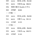
図2はこの種の命令列の一例を示す図である。図2の例では、まず、プログラムカウンタ5が000のときに、ROMアドレスレジスタ4に100番地のアドレスを記憶する。プログラムカウンタ5が001になると、強制分岐先PCレジスタ6に10番地のアドレスを記憶する。プログラムカウンタ5が002になると、強制分岐を許可する。プログラムカウンタ5が003になると、80番地に分岐して、更新されたプログラムを実行する。
【0027】
その後、プログラムカウンタ5が010になると、次の誤り箇所をROMレジスタに記憶し、011で強制分岐先PCレジスタ6を記憶する。以降、プログラムカウンタ5が030になった場合も、同様の処理が行われる。
【0028】
このように、本実施形態では、ROMアドレスレジスタ4と強制分岐先PCレジスタ6に、データバス10を経由して複数種類のアドレスを繰返し記憶できるようにしたため、プログラムROM1中のマイクロコードに複数の誤りがあっても、回路規模を増大することなく、各誤りに対応する更新マイクロコードを実行できる。このため、プログラムの保守性がよくなる。
【0029】
図1のプロセッサシステムは、プログラムROM1のデバックにも利用できる。この場合、図1の点線で示すように、マイコンIFに接続されたホストコンピュータからの指示によりデバックを行う。デバックには、プログラムROM1内の指定されたアドレス位置だけブレークさせてデバックする手法と、プログラムROM1内のプログラムを1ステップずつ実行する手法の2種類がある。
【0030】
前者の場合、以下の手順でデバックを行う。
【0031】
(1)まず、ホストコンピュータからマイコンIFを介してプログラムRAM3に、デバックプログラムを格納する。
【0032】
(2)次に、ホストコンピュータからマイコンIFを介してROMアドレスレジスタ4に、プログラムROM1内のデバックを行う先頭アドレスを記憶する。同様に、強制分岐先PCレジスタ6に、デバック時の分岐先アドレス(この場合、プログラムRAM3内のデバックプログラムの先頭アドレス)を記憶する。
【0033】
(3)次に、プログラムROM1を開始する。
【0034】
(4)プログラムカウンタ5がROMアドレスレジスタ4の値に一致すると、強制分岐先PCレジスタ6の値に基づいて、プログラムRAM3内のデバックプログラムが実行される。
【0035】
(5)このデバックプログラムでは、例えば、任意のメモリ及びレジスタの値をマイコンIFを介してホストコンピュータに伝送するという処理を実行する。
【0036】
(6)これにより、プログラムROM1内の任意のアドレス範囲についてデバックを行うことができる。また、デバックプログラムの中で、ROMアドレスレジスタ4と強制分岐先PCレジスタ6に新たな値を記憶することもでき、プログラムROM1内の複数箇所について連続的にデバックを行うことも可能である。
【0037】
(7)デバックプログラムの中で間接アドレッシングまたはスタックを利用したリターンを行って、元のプログラムROM1の処理に戻る。
【0038】
(8)以降、(3)〜(7)の処理を繰り返す。
【0039】
プログラムROM1内のプログラムを1ステップずつ実行する場合は、(1)〜(6)の手順は同じである。
【0040】
(7)次に、デバックプログラムの中でROMアドレスレジスタ4を+1する。
【0041】
(8)次に、(3)〜(7)の処理を繰り返す。
【0042】
このように、本実施形態によれば、デバック用の専用のハードウェアを設けなくても、プログラムROM1内のプログラムのデバックも行うことができる。このため、プログラムの開発が容易になる。
【0043】
【発明の効果】
以上詳細に説明したように、本発明によれば、第1及び第2のアドレス記憶部に記憶されている第1及び第2のアドレスを、データバスを介して更新できるため、第1のプログラムに複数箇所の誤りがあっても、回路規模を大きくすることなく、各誤りに対応した複数の更新プログラムを実行できる。したがって、プログラムの保守性がよくなる。
【図面の簡単な説明】
【図1】本発明に係るプロセッサシステムの一実施形態のブロック図。
【図2】プログラムRAMに格納されるプログラムの一例を示す図。
【図3】従来のプロセッサシステムの概略構成を示すブロック図。
【符号の説明】
1 プログラムROM
2 インストラクションデコーダ
3 プログラムRAM
4 ROMアドレスレジスタ
5 プログラムカウンタ
6 強制分岐先PCレジスタ
7 アドレス比較部
8 セレクタ
9 マイコンIF部
10 データバス
11 ホストコンピュータ[0001]
TECHNICAL FIELD OF THE INVENTION
The present invention relates to a processor system capable of updating or debugging at least a part of a first program stored in a first program storage unit.
[0002]
[Prior art]
One-chip microcomputers (hereinafter, one-chip microcomputers) often include a mask ROM inside. This type of mask ROM incorporates microcode in advance at the time of manufacture, but since mask ROM cannot rewrite data, if there is an error in the microcode, the microcomputer itself must be replaced and maintenance is required. Poor performance and cost in case of failure.
[0003]
In order to solve such a problem, a processor system has been put into practical use in which, when an error is found in a microcode in a program ROM, only the erroneous portion can be updated.
[0004]
FIG. 3 is a block diagram showing a schematic configuration of a conventional processor system of this kind. The processor system of FIG. 3 includes a
[0005]
The
[0006]
The
[0007]
For example, if there is an error in a specific location of the microcode stored in the
[0008]
[Problems to be solved by the invention]
However, when there are a plurality of errors in the microcode, the
[0009]
Further, the processor system of FIG. 3 merely replaces an erroneous microcode with a correct microcode, and does not have a function of debugging the microcode in the
[0010]
The present invention has been made in view of such a point, and an object of the present invention is to provide a processor system capable of correcting errors at a plurality of points in a program without increasing the circuit scale. .
[0011]
[Means for Solving the Problems]
In order to solve the above-described problems, the present invention provides a first program storage unit that stores a first program, a second program storage unit that stores a second program, and the first and second programs. A program counter for outputting an execution address of the program, a first address storage unit for storing a first address in the first program, and a second address for storing a second address in the second program An address storage unit, a comparing unit that determines whether the program counter matches the first address, and when the comparing unit determines that the program counter matches the first address, the program counter is changed to the second address. The first address stored in the first address storage unit and the second address stored in the second address storage unit. And a data bus for.
[0012]
According to the present invention, the first and second addresses can be repeatedly stored in the first and second address storage units. Therefore, even if there are a plurality of errors in the first program, the first and second addresses can be stored without increasing the circuit scale. The update program can be executed, and the maintainability of the program is improved.
[0013]
BEST MODE FOR CARRYING OUT THE INVENTION
Hereinafter, a processor system according to the present invention will be specifically described with reference to the drawings.
[0014]
FIG. 1 is a block diagram of one embodiment of a processor system according to the present invention. The processor system of FIG. 1 stores a
[0015]
The processor system of FIG. 1 differs from the processor system of FIG. 3 in that an
[0016]
Hereinafter, the processing procedure of the microcode update processing will be described. In the following description, it is assumed that the microcode in the
[0017]
(1) First, a ROM address indicating a temporally first error location in the microcode is externally stored in the
[0018]
(2) Thereafter, the
[0019]
(3) At the same time, the
[0020]
(4) When a match is detected in (3) above, the
[0021]
(5) Since the forced branch destination address indicates the updated microcode in the
[0022]
(6) The
[0023]
(7) Thereafter, the above processes (2) to (6) are repeated.
[0024]
As a method of storing an address in the
[0025]
In the latter case, for example, an instruction to store the addresses of the
[0026]
FIG. 2 is a diagram showing an example of this type of instruction sequence. In the example of FIG. 2, first, when the
[0027]
Thereafter, when the
[0028]
As described above, in the present embodiment, since a plurality of types of addresses can be repeatedly stored in the
[0029]
The processor system shown in FIG. 1 can also be used for debugging the
[0030]
In the former case, debugging is performed in the following procedure.
[0031]
(1) First, a debug program is stored in the
[0032]
(2) Next, the head address of the
[0033]
(3) Next, the
[0034]
(4) When the
[0035]
(5) In the debug program, for example, a process of transmitting an arbitrary memory and register values to the host computer via the microcomputer IF is executed.
[0036]
(6) Thus, debugging can be performed for an arbitrary address range in the
[0037]
(7) Return is performed using indirect addressing or a stack in the debug program, and the process returns to the original program ROM1.
[0038]
(8) Thereafter, the processing of (3) to (7) is repeated.
[0039]
When the program in the
[0040]
(7) Next, the
[0041]
(8) Next, the processes of (3) to (7) are repeated.
[0042]
As described above, according to the present embodiment, it is possible to debug a program in the
[0043]
【The invention's effect】
As described above in detail, according to the present invention, the first and second addresses stored in the first and second address storage units can be updated via the data bus. Even if there are a plurality of errors, a plurality of update programs corresponding to each error can be executed without increasing the circuit scale. Therefore, the maintainability of the program is improved.
[Brief description of the drawings]
FIG. 1 is a block diagram of an embodiment of a processor system according to the present invention.
FIG. 2 is a diagram showing an example of a program stored in a program RAM.
FIG. 3 is a block diagram showing a schematic configuration of a conventional processor system.
[Explanation of symbols]
1 Program ROM
2
4
Claims (7)
第2のプログラムを格納する第2のプログラム記憶部と、
前記第1及び第2のプログラムの実行アドレスを出力するプログラムカウンタと、
前記第1のプログラム中の第1のアドレスを記憶する第1のアドレス記憶部と、
前記第2のプログラム中の第2のアドレスを記憶する第2のアドレス記憶部と、
前記プログラムカウンタが前記第1のアドレスに一致したか否かを判断する比較部と、
前記比較部により一致したと判断されると、前記プログラムカウンタを前記第2のアドレスに変更するアドレス変更部と、
前記第1のアドレス記憶部に記憶される前記第1のアドレスと前記第2のアドレス記憶部に記憶される前記第2のアドレスとを更新するためのデータバスと、を備えることを特徴とするプロセッサシステム。A first program storage unit for storing a first program;
A second program storage unit for storing a second program;
A program counter for outputting execution addresses of the first and second programs;
A first address storage unit that stores a first address in the first program;
A second address storage unit for storing a second address in the second program;
A comparing unit that determines whether the program counter matches the first address;
An address changing unit that changes the program counter to the second address when the comparison unit determines that they match;
A data bus for updating the first address stored in the first address storage unit and the second address stored in the second address storage unit. Processor system.
前記第1のアドレス記憶部に記憶される前記第1のアドレスと前記第2のアドレス記憶部に記憶される前記第2のアドレスとは、前記命令デコーダの出力に基づいて更新されることを特徴とする請求項1に記載のプロセッサシステム。An instruction decoder for supplying a result obtained by decoding instructions read from the first and second program storage units to the data bus,
The first address stored in the first address storage unit and the second address stored in the second address storage unit are updated based on an output of the instruction decoder. The processor system according to claim 1, wherein
前記第1のアドレス記憶部は、前記第1のプログラムに従って、それぞれ異なるタイミングで複数種類の前記第1のアドレスを順次記憶し、
前記第2のアドレス記憶部は、前記第1のプログラムに従って、それぞれ異なるタイミングで複数種類の前記第2のアドレスを順次記憶することを特徴とする請求項2に記載のプロセッサシステム。The first program stores a plurality of instructions for storing a plurality of types of the first addresses in the first address storage unit, and stores a plurality of types of the second addresses in the second address, respectively. A plurality of instructions for storing in the unit;
The first address storage unit sequentially stores a plurality of types of the first addresses at different timings according to the first program,
The processor system according to claim 2, wherein the second address storage unit sequentially stores a plurality of types of the second addresses at different timings according to the first program.
前記第2のプログラム記憶部は、書き換え可能なメモリであり、
前記第2のプログラムは、前記第1のプログラムの少なくとも一部を更新するためのプログラムであることを特徴とする請求項1及至4のいずれかに記載のプロセッサシステム。The first program storage unit is a ROM,
The second program storage unit is a rewritable memory,
The processor system according to claim 1, wherein the second program is a program for updating at least a part of the first program.
前記第1のアドレスは、前記第1のプログラム中のデバックを行う箇所の先頭アドレスであり、
前記第2のアドレスは、前記デバックプログラムの先頭アドレスであることを特徴とする請求項1,2,3及び5のいずれかに記載のプロセッサシステム。The second program is a debugging program for debugging an arbitrary part in the first program,
The first address is a head address of a location in the first program where debugging is performed,
6. The processor system according to claim 1, wherein the second address is a head address of the debug program.
Priority Applications (4)
| Application Number | Priority Date | Filing Date | Title |
|---|---|---|---|
| JP2002285740A JP2004126658A (en) | 2002-09-30 | 2002-09-30 | Processor system |
| EP03021630A EP1403768A3 (en) | 2002-09-30 | 2003-09-25 | Processor system, processor and arithmetic processing method |
| US10/670,233 US7203867B2 (en) | 2002-09-30 | 2003-09-26 | Processor system, processor and arithmetic processing method |
| CNB03127238XA CN1270249C (en) | 2002-09-30 | 2003-09-30 | Processor system, processor and operation processing method |
Applications Claiming Priority (1)
| Application Number | Priority Date | Filing Date | Title |
|---|---|---|---|
| JP2002285740A JP2004126658A (en) | 2002-09-30 | 2002-09-30 | Processor system |
Publications (2)
| Publication Number | Publication Date |
|---|---|
| JP2004126658A true JP2004126658A (en) | 2004-04-22 |
| JP2004126658A5 JP2004126658A5 (en) | 2005-01-06 |
Family
ID=31973404
Family Applications (1)
| Application Number | Title | Priority Date | Filing Date |
|---|---|---|---|
| JP2002285740A Abandoned JP2004126658A (en) | 2002-09-30 | 2002-09-30 | Processor system |
Country Status (4)
| Country | Link |
|---|---|
| US (1) | US7203867B2 (en) |
| EP (1) | EP1403768A3 (en) |
| JP (1) | JP2004126658A (en) |
| CN (1) | CN1270249C (en) |
Cited By (1)
| Publication number | Priority date | Publication date | Assignee | Title |
|---|---|---|---|---|
| JP2008015792A (en) * | 2006-07-06 | 2008-01-24 | Fujitsu Ltd | Rom patch processing method and rom patch device |
Families Citing this family (4)
| Publication number | Priority date | Publication date | Assignee | Title |
|---|---|---|---|---|
| US8418023B2 (en) | 2007-05-01 | 2013-04-09 | The Texas A&M University System | Low density parity check decoder for irregular LDPC codes |
| CN101923495B (en) * | 2009-06-10 | 2012-11-14 | Tcl集团股份有限公司 | Embedded fault tolerant system and fault tolerant method thereof |
| NO332162B1 (en) * | 2009-12-21 | 2012-07-09 | Cisco Systems Int Sarl | Device and method for filtering media packages |
| WO2018235403A1 (en) * | 2017-06-23 | 2018-12-27 | 日立オートモティブシステムズ株式会社 | Electronic control device |
Family Cites Families (11)
| Publication number | Priority date | Publication date | Assignee | Title |
|---|---|---|---|---|
| US5357627A (en) * | 1989-03-28 | 1994-10-18 | Olympus Optical Co., Ltd. | Microcomputer having a program correction function |
| TW231343B (en) * | 1992-03-17 | 1994-10-01 | Hitachi Seisakusyo Kk | |
| JPH05298462A (en) | 1992-04-23 | 1993-11-12 | Sony Corp | Electronic device |
| JPH0744419A (en) * | 1993-08-03 | 1995-02-14 | Nec Ic Microcomput Syst Ltd | Microcomputer development back up device |
| JPH0895946A (en) | 1994-09-22 | 1996-04-12 | Nec Corp | Microcomputer |
| JPH08166877A (en) * | 1994-12-13 | 1996-06-25 | Olympus Optical Co Ltd | One-chip microcomputer that can execute correction program and microcomputer that can correct rom |
| US6023758A (en) * | 1995-05-25 | 2000-02-08 | Matsushita Electric Industrial Co., Ltd. | Method and processor for changing program by replacing instruction stored in ROM with predetermined value to be interpreted as an instruction |
| JPH09319727A (en) * | 1996-05-31 | 1997-12-12 | Hitachi Ltd | Data processor and data processing system |
| TW400469B (en) * | 1997-07-08 | 2000-08-01 | Winbond Electronics Corp | Device capable of fixing programs in embedded microprocessor |
| CN1088868C (en) | 1997-08-08 | 2002-08-07 | 华邦电子股份有限公司 | Patch device for program in embedded microprocessor system |
| US6973522B1 (en) * | 1999-08-10 | 2005-12-06 | Pentax Corporation | Microcomputer with program-revision ability |
-
2002
- 2002-09-30 JP JP2002285740A patent/JP2004126658A/en not_active Abandoned
-
2003
- 2003-09-25 EP EP03021630A patent/EP1403768A3/en not_active Withdrawn
- 2003-09-26 US US10/670,233 patent/US7203867B2/en active Active
- 2003-09-30 CN CNB03127238XA patent/CN1270249C/en not_active Expired - Fee Related
Cited By (1)
| Publication number | Priority date | Publication date | Assignee | Title |
|---|---|---|---|---|
| JP2008015792A (en) * | 2006-07-06 | 2008-01-24 | Fujitsu Ltd | Rom patch processing method and rom patch device |
Also Published As
| Publication number | Publication date |
|---|---|
| EP1403768A3 (en) | 2007-05-02 |
| US20040153829A1 (en) | 2004-08-05 |
| CN1497460A (en) | 2004-05-19 |
| CN1270249C (en) | 2006-08-16 |
| US7203867B2 (en) | 2007-04-10 |
| EP1403768A2 (en) | 2004-03-31 |
Similar Documents
| Publication | Publication Date | Title |
|---|---|---|
| JPS58151648A (en) | Data processor having program patching means | |
| JPH06318261A (en) | Electronic device | |
| CN112947977A (en) | Software online upgrading method and system | |
| JP2875842B2 (en) | Programmable controller | |
| US6925522B2 (en) | Device and method capable of changing codes of micro-controller | |
| JP2004046453A (en) | Single chip microcomputer and boot sector switching method | |
| JP2004126658A (en) | Processor system | |
| CN110442074B (en) | Processing device for programmable logic controller program | |
| JP2004038541A (en) | Memory check system, memory check method, signal processor, memory check method of signal processor, and memory check program | |
| JP2001256044A (en) | Data processor | |
| JP2004240717A (en) | Software updating device | |
| KR20010015000A (en) | Computer system having a rom correction unit | |
| JP2003177934A (en) | Digital signal processor | |
| JP2010157026A (en) | Program area change method | |
| JP3105822B2 (en) | Micro program controller | |
| KR20020029921A (en) | Method and apparatus for modifying microinstructions in a static memory device | |
| JP2003122575A (en) | Information processing unit | |
| JPH06187140A (en) | Processor | |
| JPS63156231A (en) | Changing method for instruction in read-only memory | |
| JPH1040094A (en) | Program controller for firmware | |
| US7003543B2 (en) | Sticky z bit | |
| JP2003178596A (en) | Semiconductor integrated circuit | |
| JPS5816349A (en) | Memory extension substituting system | |
| JP2005063311A (en) | Patch method and patch application program for processor system | |
| JP2000259403A (en) | Device and method for batch processing |
Legal Events
| Date | Code | Title | Description |
|---|---|---|---|
| A521 | Written amendment |
Free format text: JAPANESE INTERMEDIATE CODE: A523 Effective date: 20040213 |
|
| A621 | Written request for application examination |
Free format text: JAPANESE INTERMEDIATE CODE: A621 Effective date: 20040213 |
|
| A131 | Notification of reasons for refusal |
Free format text: JAPANESE INTERMEDIATE CODE: A131 Effective date: 20060414 |
|
| A762 | Written abandonment of application |
Free format text: JAPANESE INTERMEDIATE CODE: A762 Effective date: 20060613 |