EP1403768A2 - Processor system, processor and arithmetic processing method - Google Patents
Processor system, processor and arithmetic processing method Download PDFInfo
- Publication number
- EP1403768A2 EP1403768A2 EP20030021630 EP03021630A EP1403768A2 EP 1403768 A2 EP1403768 A2 EP 1403768A2 EP 20030021630 EP20030021630 EP 20030021630 EP 03021630 A EP03021630 A EP 03021630A EP 1403768 A2 EP1403768 A2 EP 1403768A2
- Authority
- EP
- European Patent Office
- Prior art keywords
- program
- address
- storage
- stored
- addresses
- Prior art date
- Legal status (The legal status is an assumption and is not a legal conclusion. Google has not performed a legal analysis and makes no representation as to the accuracy of the status listed.)
- Withdrawn
Links
Images


Classifications
-
- G—PHYSICS
- G06—COMPUTING; CALCULATING OR COUNTING
- G06F—ELECTRIC DIGITAL DATA PROCESSING
- G06F11/00—Error detection; Error correction; Monitoring
- G06F11/36—Preventing errors by testing or debugging software
- G06F11/362—Software debugging
- G06F11/3648—Software debugging using additional hardware
Definitions
- the present invention relates to a processor system, a processor and a method of arithmetic processing method capable of updating and debugging at least portion of a first program stored in a first program storage.
- a one chip micro computer ordinarily contains a mask ROM.
- Micro codes are embedded in such kind of mask ROM at manufactured time in advance. Since the mask ROM cannot rewrite data, if the micro codes include errors, the micro computer by itself has to be exchanged. Therefore, maintainability is not good, and it takes too much cost to revise the micro codes.
- Such kind of conventional processor system has a program RAM in which the correct micro codes are stored, a ROM address register in which erroneous addresses of the micro codes in the program ROM are stored, a forced branch destination PC register in which addresses to be executed in the program RAM are stored, and an address comparator for determining whether or not a program counter coincides with erroneous addresses stored in the ROM address register.
- the processor system changes a value of the program counter into a value of the forced branch destination PC register. Therefore, correct micro codes stored in the program RAM are executed.
- a processor system comprising:
- arithmetic processing method comprising:
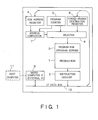
- Fig. 1 is a block diagram of a processor system according to one embodiment of the present invention.
- the processor system of Fig. 1 has a program ROM 1 for storing micro codes, an instruction decoder 2 for decoding instructions included in the micro codes, a program RAM 3 for storing the updated micro codes in which errors in the micro codes has been revised, an ROM address register 4 for storing addresses indicative of errors in the micro codes stored in the program RAM 1, a forced branch destination PC register 6 for storing a branch destination address when the micro codes include errors, an address comparator 7 for detecting whether the address stored in the address register 4 coincide with the program counter 5, a selector 8 for changing the program counter 5 into the branch destination address when both addresses coincide with each other, a micro computer IF unit 9 (an external IF unit) for transferring data for outside.
- a program ROM 1 for storing micro codes
- an instruction decoder 2 for decoding instructions included in the micro codes
- a program RAM 3 for storing the updated micro codes in which errors in the micro codes has been revised
- the instruction decoder 2 the ROM address register 4, the forced branch destination register 6 and the micro computer IF unit 6 are connected to a common data bus 10.
- Fig. 1 All the constituents of Fig. 1 may be contained in the one chip IC. Or a chip for the processor may be provided separate from a chip for a peripheral memory. In the case of providing separate chips, the processor has, for example, the instruction decoder 2 of Fig. 1, the ROM address register 4, the program counter 5, the forced branch destination register 6, the address comparator 7, the selector 8 and the micro computer IF 9.
- Fig. 2 is a flowchart showing processing operations of the processor system of Fig. 1. Hereinafter, the processing operations of this embodiment will be described with reference to Figs. 1 and 2. It is assumed that the micro codes in the program ROM 1 include a plurality of errors.
- the ROM address indicative of an error location at first time is stored in the ROM address register 4 from outside via the micro computer IF unit and a data bus 10.
- the address of the program RAM 3 in which the updated micro codes are stored is stored in the forced branch destination PC register from outside via the micro computer IF unit 9 and the data bus 10 (step S1).
- step S2 Instructions are read out from the program ROM 1 by setting the program counter 5 as an address, the instruction is decoded by the instruction decoder 2, and the instruction is executed (step S3).
- the address comparator 7 detects whether or not the program counter 5 coincides with the ROM address stored in the ROM address register 4 (step S4). If not coincided, the processings of steps S2 and S3 are repeated.
- the selector 8 changes the program counter 5 into the forced branch destination address stored in the forced branch destination PC register 6 (step S5).
- the forced branch destination address indicates the updated micro codes in the program RAM 3. Therefore, instead of the erroneous micro codes in the program ROM 1, the updated micro codes in the program RAM 3 are executed.
- the ROM address register 4 stores the address indicative of a next erroneous location of the micro codes in the program ROM 1. Similarly, the addresses of the updated micro codes in the program RAM 3 are stored in the forced branch destination PC register (S6). Subsequently, the processings of steps S2-S6 are repeated.
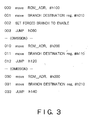
- Fig. 3 is a diagram showing one example of such kind of instruction strings.
- the program counter 5 when the program counter 5 is "000", the address "100" is stored in the ROM address register 4.
- the program counter 5 becomes "001” the address "10” is stored in the forced branch destination PC register 6.
- the program counter 5 becomes "002” the forced branch is allowed.
- the program counter 6 branches to the address "80" to execute the updated program.
- a plurality of addresses can be repeatedly stored via the data bus 10 in the ROM address register 4 and the forced branch destination PC register 6. Because of this, even if the micro codes in the program ROM 1 include a plurality of errors, it is possible to execute the updated micro codes corresponding to the errors, without increasing the circuit size, thereby improving maintainability of the program.
- the processor system of Fig. 1 can be used even to the debug of the program ROM 1.
- the debug is carried out by the instruction of the host computer connected to the micro computer IF.
- the debug program is stored from the host computer 1, via the micro computer IF, into the program RAM 3 (step S11). Subsequently, a head address for performing the debug of the program ROM 1 is stored from the host computer 11, via the micro computer IF, into the ROM address register 4. Similarly, the branch destination address at debug time (in this case, the head address of the debug program in the program RAM 3) is stored in the forced branch destination PC register 6 (step S12).
- step S13 execution of the program in the program ROM 1 is begun.
- step S14 execution of the program in the program ROM 1 is begun.
- the processing for transferring the value of an arbitrary memory and register via the micro computer IF, to the host computer 11 is carried out. Therefore, it is possible to perform the debug with regard to an arbitrary address range in the program ROM 1 (step S15).
- the debug program it is possible to store a new value in the ROM address register 4 and the forced branch destination PC register 6, and to continuously perform the debug with regard to a plurality of locations in the program ROM 1.
- step S16 it is determined whether or not the debug processings are finished. If determined to be finished, the processings of Fig. 4 are ended. If determined not to be finished, indirect addressing or return using stack is performed in the debug program, in order to return to the processings of the original program ROM 1 (step S17). Hereinafter, the processings of steps S13-S16 are repeated.
- steps S11-S14 are the same.
- the ROM address register 4 is incremented in the debug program.
- the processings after steps S13 are repeated.
Landscapes
- Engineering & Computer Science (AREA)
- Computer Hardware Design (AREA)
- Theoretical Computer Science (AREA)
- Quality & Reliability (AREA)
- Physics & Mathematics (AREA)
- General Engineering & Computer Science (AREA)
- General Physics & Mathematics (AREA)
- Debugging And Monitoring (AREA)
- Hardware Redundancy (AREA)
- Stored Programmes (AREA)
Abstract
Description
- The present invention relates to a processor system, a processor and a method of arithmetic processing method capable of updating and debugging at least portion of a first program stored in a first program storage.
- A one chip micro computer ordinarily contains a mask ROM. Micro codes are embedded in such kind of mask ROM at manufactured time in advance. Since the mask ROM cannot rewrite data, if the micro codes include errors, the micro computer by itself has to be exchanged. Therefore, maintainability is not good, and it takes too much cost to revise the micro codes.
- In order to overcome such a problem, a processor system in which when the micro codes in the program ROM include the errors, only the erroneous portions can be updated has been realized.
- Such kind of conventional processor system has a program RAM in which the correct micro codes are stored, a ROM address register in which erroneous addresses of the micro codes in the program ROM are stored, a forced branch destination PC register in which addresses to be executed in the program RAM are stored, and an address comparator for determining whether or not a program counter coincides with erroneous addresses stored in the ROM address register. The processor system changes a value of the program counter into a value of the forced branch destination PC register. Therefore, correct micro codes stored in the program RAM are executed.
- When the micro codes include a plurality of errors, however, the ROM address register and the forced branch destination PC register has to be provided by each erroneous location. Therefore, circuit size becomes large.
- Although such kind of conventional processor system replaces the erroneous micro codes with correct micro codes, the system does not have a function for debugging the micro codes in the program ROM. Because of this, in order to perform the debug, a debug dedicated circuit has to be added to the processor system, thereby increasing the circuit size.
- A processor system according to one embodiment of the present invention, comprising:
- a first program storage which stores a first program;
- a second program storage which stores a second program;
- a program counter which outputs execution addresses of said first and second programs;
- a first address storage which stores a first address in said first program;
- a second address storage which stores a second address in said second program;
- a comparator which compares whether or not said program counter coincides with said first address;
- an address changing unit which changes said program counter to said second address, when it is determined to have coincided by said comparator; and
- a data bus which updates said first address stored in said first address storage and said second address stored in said second address storage.
- Furthermore, a arithmetic processing method, comprising:
- outputting from a program counter execution addresses of a first program stored in a first program storage and a second program stored in a second program storage;
- determining whether or not said program counter coincides with a first address in said first program stored in said first address storage; and
- changing said program counter into a second address in said second program stored in said second address storage, when it is determined to have coincided.
-
- Fig. 1 is a block diagram of a processor system according to one embodiment of the present invention.
- Fig. 2 is a flowchart showing processing operations of a processor system of Fig. 1.
- Fig. 3 is a diagram showing one example of such kinds of instruction strings.
- Fig. 4 is a flowchart showing processing procedure in the case of debugging.
- Hereinafter, a processor system, a processor and an arithmetic processing method according to one embodiment of the present invention will be more specifically described with reference to drawings.
- Fig. 1 is a block diagram of a processor system according to one embodiment of the present invention. The processor system of Fig. 1 has a
program ROM 1 for storing micro codes, aninstruction decoder 2 for decoding instructions included in the micro codes, aprogram RAM 3 for storing the updated micro codes in which errors in the micro codes has been revised, anROM address register 4 for storing addresses indicative of errors in the micro codes stored in theprogram RAM 1, a forced branchdestination PC register 6 for storing a branch destination address when the micro codes include errors, anaddress comparator 7 for detecting whether the address stored in theaddress register 4 coincide with theprogram counter 5, aselector 8 for changing theprogram counter 5 into the branch destination address when both addresses coincide with each other, a micro computer IF unit 9 (an external IF unit) for transferring data for outside. - In the processor system of Fig. 1, the
instruction decoder 2, theROM address register 4, the forcedbranch destination register 6 and the microcomputer IF unit 6 are connected to acommon data bus 10. - All the constituents of Fig. 1 may be contained in the one chip IC. Or a chip for the processor may be provided separate from a chip for a peripheral memory. In the case of providing separate chips, the processor has, for example, the
instruction decoder 2 of Fig. 1, theROM address register 4, theprogram counter 5, the forcedbranch destination register 6, theaddress comparator 7, theselector 8 and the micro computer IF 9. - Fig. 2 is a flowchart showing processing operations of the processor system of Fig. 1. Hereinafter, the processing operations of this embodiment will be described with reference to Figs. 1 and 2. It is assumed that the micro codes in the
program ROM 1 include a plurality of errors. - First of all, the ROM address indicative of an error location at first time is stored in the
ROM address register 4 from outside via the micro computer IF unit and adata bus 10. Similarly, the address of theprogram RAM 3 in which the updated micro codes are stored is stored in the forced branch destination PC register from outside via the microcomputer IF unit 9 and the data bus 10 (step S1). - Afterward, the
program counter 5 begins count-up operation (step S2). Instructions are read out from theprogram ROM 1 by setting theprogram counter 5 as an address, the instruction is decoded by theinstruction decoder 2, and the instruction is executed (step S3). - In parallel with the processing, the
address comparator 7 detects whether or not theprogram counter 5 coincides with the ROM address stored in the ROM address register 4 (step S4). If not coincided, the processings of steps S2 and S3 are repeated. - If coincided, the
selector 8 changes theprogram counter 5 into the forced branch destination address stored in the forced branch destination PC register 6 (step S5). - The forced branch destination address indicates the updated micro codes in the
program RAM 3. Therefore, instead of the erroneous micro codes in theprogram ROM 1, the updated micro codes in theprogram RAM 3 are executed. - The ROM address register 4 stores the address indicative of a next erroneous location of the micro codes in the
program ROM 1. Similarly, the addresses of the updated micro codes in theprogram RAM 3 are stored in the forced branch destination PC register (S6). Subsequently, the processings of steps S2-S6 are repeated. - As a method of storing the addresses in the
ROM address register 4 or the forced branch destination PC register in the above steps S1 and S6, there are a method of storing the address supplied from outside as mentioned above in the registers via the micro computer IF and thedatabase 10, and a method of storing the addresses in the registers based on the program in theprogram RAM 3. - In the case of the latter, for example, the instructions for storing the addresses of the
ROM address register 4 and the forced branchdestination PC register 6 are described in the program of theprogram RAM 3. - Fig. 3 is a diagram showing one example of such kind of instruction strings. In the example of Fig. 3, first of all, when the
program counter 5 is "000", the address "100" is stored in theROM address register 4. When theprogram counter 5 becomes "001", the address "10" is stored in the forced branchdestination PC register 6. When theprogram counter 5 becomes "002", the forced branch is allowed. When theprogram counter 5 becomes "003", the program counter 6 branches to the address "80" to execute the updated program. - Afterward, when the
program counter 5 becomes "010", a next erroneous location is stored in the ROM register, and when theprogram counter 5 becomes "011", the forced branchdestination PC register 6 is stored. Subsequently, even when theprogram counter 5 has become "030", the same processings are performed. - As described above, according to the present embodiment, a plurality of addresses can be repeatedly stored via the
data bus 10 in theROM address register 4 and the forced branchdestination PC register 6. Because of this, even if the micro codes in theprogram ROM 1 include a plurality of errors, it is possible to execute the updated micro codes corresponding to the errors, without increasing the circuit size, thereby improving maintainability of the program. - The processor system of Fig. 1 can be used even to the debug of the
program ROM 1. In this case, as shown in a dotted line of Fig. 1, the debug is carried out by the instruction of the host computer connected to the micro computer IF. There are a method of performing the debug while breaking the program as many as the address locations designated in theROM 1, and a method of executing the program in theprogram ROM 1 by each step. - In the case of the former, the debug program is stored from the
host computer 1, via the micro computer IF, into the program RAM 3 (step S11). Subsequently, a head address for performing the debug of theprogram ROM 1 is stored from thehost computer 11, via the micro computer IF, into theROM address register 4. Similarly, the branch destination address at debug time (in this case, the head address of the debug program in the program RAM 3) is stored in the forced branch destination PC register 6 (step S12). - Subsequently, execution of the program in the
program ROM 1 is begun (step S13). When theprogram counter 5 coincides with the value of theROM address register 4, the debug program in theprogram RAM 3 is executed based on the value of the forced branch destination PC register 6 (step S14). - In the debug program, for example, the processing for transferring the value of an arbitrary memory and register via the micro computer IF, to the
host computer 11 is carried out. Therefore, it is possible to perform the debug with regard to an arbitrary address range in the program ROM 1 (step S15). In the debug program, it is possible to store a new value in theROM address register 4 and the forced branchdestination PC register 6, and to continuously perform the debug with regard to a plurality of locations in theprogram ROM 1. - Next, it is determined whether or not the debug processings are finished (step S16). If determined to be finished, the processings of Fig. 4 are ended. If determined not to be finished, indirect addressing or return using stack is performed in the debug program, in order to return to the processings of the original program ROM 1 (step S17). Hereinafter, the processings of steps S13-S16 are repeated.
- When the program in the
program ROM 1 is executed by each step, the processing procedures of steps S11-S14 are the same. After the execution of the debug program is begun in step S14, theROM address register 4 is incremented in the debug program. Next, the processings after steps S13 are repeated. - As described above, according to this embodiment, even if a dedicated hardware for debug is not provided, it is possible to perform debug of the program in the
ROM 1. Because of this, it is possible to make easy development of the program.
Claims (20)
- A processor system, comprising:a first program storage which stores a first program;a second program storage which stores a second program;a program counter which outputs execution addresses of said first and second programs;a first address storage which stores a first address in said first program;a second address storage which stores a second address in said second program;a comparator which compares whether or not said program counter coincides with said first address;an address changing unit which changes said program counter to said second address, when it is determined to have coincided by said comparator; anda data bus which updates said first address stored in said first address storage and said second address stored in said second address storage.
- The processor system according to claim 1, further comprising an instruction decoder which provides a result of decoding instructions read out from said first and second program storages to said data bus,
wherein said first address stored in said first address storage and said second address stored in said second address storage are updated based on output of said instruction decoder. - The processor system according to claim 2, wherein said first program includes:a plurality of instructions which store a plurality of first addresses in said first address storage; anda plurality of instructions which store a plurality of second addresses in said second address storage,wherein said first address storage stores a plurality of first addresses in sequence, in accordance with said first program at timing different from each other; and
said second address storage stores a plurality of second addresses in sequence, in accordance with said first program at timing different from each other. - The processor system according to claim 1, further comprising an interface unit which performs control for storing said first and second addresses supplied from outside, via said data bus, in said first and second program storages.
- The processor system according to claim 1, wherein said first program storage is an ROM;
said second program storage is a rewritable memory; and
said second program is a program which updates at least portion of said first program. - The processor system according to claim 1, wherein said second program is a debug program which performs a debug at an arbitrary location in said first program;
said first address is a head address at a location which performs the debug in said first program; and
said second address is a head address of said debug program. - The processor system according to claim 6, further comprising an interface unit which performs control for storing said second program, said first address and said second address supplied from outside via said data bus, in said second program storage, said first address storage and said second address storage, respectively, and performs control for supplying a result of executing said debug program to outside.
- A processor, comprising:a program counter which outputs execution addresses of a first program stored in a first program storage and a second program stored in a second program storage;a comparator which determines whether or not said program counter coincides with a first address in said first program stored in said first address storage;an address changing unit which changes said program counter to a second address in said second program stored in said second address storage, when it is determined to have coincided by said comparator; anda data bus which updates said first address stored in said first address storage and said second address stored in said second address storage.
- The processor according to claim 8, further comprising an instruction decoder which supplies a result of decoding instructions read out from said first and second program to said data bus,
wherein said first address stored in said first address storage and said second address stored in said second address storage are updated based on the output of said instruction decoder. - The processor according to claim 9, wherein said first program includes:a plurality of instructions which store a plurality of first addresses in said first address storage; anda plurality of instructions which store a plurality of second addresses in said second address storage,the processor according to claim 9, further comprising:a first address storing controller which performs control for storing in sequence a plurality of first addresses in said first address storage at timing different from each other, in accordance with said first program; anda second address storing controller which performs control for storing in sequence a plurality of second addresses in said second address storage at timing different from each other, in accordance with said first program.
- The processor according to claim 8, further comprising an interface unit which performs control for storing said first and second addresses supplied from outside, via said data bus, in said first and second program storages.
- The processor according to claim 8, wherein said first program storage is an ROM;
said second program storage is a rewritable memory; and
said second program is a program which updates at least portion of said first program. - The processor according to claim 8, wherein said second program is a debug program which performs debug at an arbitrary location in said first program;
said first address is a head address at locations which performs debug in said first program; and
said second address is a head address of said debug program. - The processor according to claim 13, further comprising an interface unit which perform control for storing said second program, said first address and said second address supplied from outside via said data bus, in said second program storage, said first program storage and said second address storage, respectively, and performs control for supplying execution result of said debug program to outside.
- A arithmetic processing method, comprising:outputting from a program counter execution addresses of a first program stored in a first program storage and a second program stored in a second program storage;determining whether or not said program counter coincides with a first address in said first program stored in said first address storage; andchanging said program counter into a second address in said second program stored in said second address storage, when it is determined to have coincided.
- The arithmetic processing method according to claim 15, further comprising
supplying a result of decoding instructions read out from said first and second program storages to said data bus,
wherein said first address stored in said first address storage and said second address stored in said second address storage are updated based on the output of said instruction decoder. - The arithmetic processing method according to claim 16, wherein said first program includes:a plurality of instructions which store a plurality of first addresses in said first address storage; anda plurality of instructions which store a plurality of second addresses in said second address storage,and further comprising:performing control for storing in sequence a plurality of first addresses in said first address storage at timing different from each other, in accordance with said first program; andperforming control for storing in sequence a plurality of second addresses in said second address storage at timing different from each other, in accordance with said first program.
- The arithmetic processing method according to claim 15, further comprising
performing control for storing said first and second addresses supplied from outside, via said data bus, in said first and second program storages. - The arithmetic processing method according to claim 15, wherein said first program storage is an ROM;
said second program storage is a rewritable memory; and
said second program is a program which updates at least portion of said first program. - The arithmetic processing method according to claim 15, wherein said second program is a debug program which performs debug at an arbitrary location in said first program;
said first address is a head address at a location which performs debug in said first program; and
said second address is a head address of said debug program.
Applications Claiming Priority (2)
| Application Number | Priority Date | Filing Date | Title |
|---|---|---|---|
| JP2002285740 | 2002-09-30 | ||
| JP2002285740A JP2004126658A (en) | 2002-09-30 | 2002-09-30 | Processor system |
Publications (2)
| Publication Number | Publication Date |
|---|---|
| EP1403768A2 true EP1403768A2 (en) | 2004-03-31 |
| EP1403768A3 EP1403768A3 (en) | 2007-05-02 |
Family
ID=31973404
Family Applications (1)
| Application Number | Title | Priority Date | Filing Date |
|---|---|---|---|
| EP03021630A Withdrawn EP1403768A3 (en) | 2002-09-30 | 2003-09-25 | Processor system, processor and arithmetic processing method |
Country Status (4)
| Country | Link |
|---|---|
| US (1) | US7203867B2 (en) |
| EP (1) | EP1403768A3 (en) |
| JP (1) | JP2004126658A (en) |
| CN (1) | CN1270249C (en) |
Families Citing this family (5)
| Publication number | Priority date | Publication date | Assignee | Title |
|---|---|---|---|---|
| JP2008015792A (en) * | 2006-07-06 | 2008-01-24 | Fujitsu Ltd | Rom patch processing method and rom patch device |
| US8359522B2 (en) | 2007-05-01 | 2013-01-22 | Texas A&M University System | Low density parity check decoder for regular LDPC codes |
| CN101923495B (en) * | 2009-06-10 | 2012-11-14 | Tcl集团股份有限公司 | Embedded fault tolerant system and fault tolerant method thereof |
| NO332162B1 (en) * | 2009-12-21 | 2012-07-09 | Cisco Systems Int Sarl | Device and method for filtering media packages |
| US10833688B2 (en) * | 2017-06-23 | 2020-11-10 | Hitachi Automotive Systems, Ltd. | Electronic control device |
Citations (2)
| Publication number | Priority date | Publication date | Assignee | Title |
|---|---|---|---|---|
| EP0638864A1 (en) * | 1993-08-03 | 1995-02-15 | Nec Corporation | Development support system for microcomputer with internal cache |
| DE10039183A1 (en) * | 1999-08-10 | 2001-03-01 | Asahi Optical Co Ltd | Microcomputer with program revision capability performs interrupt routine based on revision program when program counter addresses match |
Family Cites Families (9)
| Publication number | Priority date | Publication date | Assignee | Title |
|---|---|---|---|---|
| US5357627A (en) * | 1989-03-28 | 1994-10-18 | Olympus Optical Co., Ltd. | Microcomputer having a program correction function |
| TW231343B (en) * | 1992-03-17 | 1994-10-01 | Hitachi Seisakusyo Kk | |
| JPH05298462A (en) | 1992-04-23 | 1993-11-12 | Sony Corp | Electronic device |
| JPH0895946A (en) | 1994-09-22 | 1996-04-12 | Nec Corp | Microcomputer |
| JPH08166877A (en) * | 1994-12-13 | 1996-06-25 | Olympus Optical Co Ltd | One-chip microcomputer that can execute correction program and microcomputer that can correct rom |
| US6023758A (en) * | 1995-05-25 | 2000-02-08 | Matsushita Electric Industrial Co., Ltd. | Method and processor for changing program by replacing instruction stored in ROM with predetermined value to be interpreted as an instruction |
| JPH09319727A (en) * | 1996-05-31 | 1997-12-12 | Hitachi Ltd | Data processor and data processing system |
| TW400469B (en) * | 1997-07-08 | 2000-08-01 | Winbond Electronics Corp | Device capable of fixing programs in embedded microprocessor |
| CN1088868C (en) | 1997-08-08 | 2002-08-07 | 华邦电子股份有限公司 | Patch device for program in embedded microprocessor system |
-
2002
- 2002-09-30 JP JP2002285740A patent/JP2004126658A/en not_active Abandoned
-
2003
- 2003-09-25 EP EP03021630A patent/EP1403768A3/en not_active Withdrawn
- 2003-09-26 US US10/670,233 patent/US7203867B2/en active Active
- 2003-09-30 CN CNB03127238XA patent/CN1270249C/en not_active Expired - Fee Related
Patent Citations (2)
| Publication number | Priority date | Publication date | Assignee | Title |
|---|---|---|---|---|
| EP0638864A1 (en) * | 1993-08-03 | 1995-02-15 | Nec Corporation | Development support system for microcomputer with internal cache |
| DE10039183A1 (en) * | 1999-08-10 | 2001-03-01 | Asahi Optical Co Ltd | Microcomputer with program revision capability performs interrupt routine based on revision program when program counter addresses match |
Also Published As
| Publication number | Publication date |
|---|---|
| EP1403768A3 (en) | 2007-05-02 |
| CN1497460A (en) | 2004-05-19 |
| US7203867B2 (en) | 2007-04-10 |
| CN1270249C (en) | 2006-08-16 |
| JP2004126658A (en) | 2004-04-22 |
| US20040153829A1 (en) | 2004-08-05 |
Similar Documents
| Publication | Publication Date | Title |
|---|---|---|
| US7454663B2 (en) | Method and circuitry for debugging/updating ROM | |
| US6745278B2 (en) | Computer capable of rewriting an area of a non-volatile memory with a boot program during self mode operation of the computer | |
| US5095426A (en) | Data processing system for effectively handling exceptions during execution of two different types of instructions | |
| US5600807A (en) | Programmable controller capable of updating a user program during operation by switching between user program memories | |
| US5479342A (en) | Microcomputer | |
| US20060026415A1 (en) | Method of updating a portion BIOS | |
| US6925522B2 (en) | Device and method capable of changing codes of micro-controller | |
| EP1403768A2 (en) | Processor system, processor and arithmetic processing method | |
| JPS5816350A (en) | Memory extension substituting system | |
| EP0577393B1 (en) | Method for executing a program | |
| KR100355630B1 (en) | Computer system having a rom correction unit | |
| US20070169086A1 (en) | System and method for updating in-system program | |
| US20010052114A1 (en) | Data processing apparatus | |
| JP3358214B2 (en) | Electronic equipment | |
| US20100125720A1 (en) | Instruction mode identification apparatus and method | |
| JPH0546378A (en) | Correction processing method for program | |
| US7281166B1 (en) | User-customizable input error handling | |
| JP2003509769A (en) | Method and apparatus for modifying microinstructions in static storage | |
| KR20080044652A (en) | Method for debugging by using stack of cpu | |
| JP2733692B2 (en) | ROM device | |
| JP3575052B2 (en) | Electronic equipment | |
| JPH1165622A (en) | Programmable controller | |
| JPH01113835A (en) | Memory fault avoiding system in information processor | |
| JPH03160524A (en) | Information processor | |
| JPH05241853A (en) | Programmable controller |
Legal Events
| Date | Code | Title | Description |
|---|---|---|---|
| PUAI | Public reference made under article 153(3) epc to a published international application that has entered the european phase |
Free format text: ORIGINAL CODE: 0009012 |
|
| 17P | Request for examination filed |
Effective date: 20030925 |
|
| AK | Designated contracting states |
Kind code of ref document: A2 Designated state(s): AT BE BG CH CY CZ DE DK EE ES FI FR GB GR HU IE IT LI LU MC NL PT RO SE SI SK TR |
|
| AX | Request for extension of the european patent |
Extension state: AL LT LV MK |
|
| PUAL | Search report despatched |
Free format text: ORIGINAL CODE: 0009013 |
|
| AK | Designated contracting states |
Kind code of ref document: A3 Designated state(s): AT BE BG CH CY CZ DE DK EE ES FI FR GB GR HU IE IT LI LU MC NL PT RO SE SI SK TR |
|
| AX | Request for extension of the european patent |
Extension state: AL LT LV MK |
|
| 17Q | First examination report despatched |
Effective date: 20071122 |
|
| AKX | Designation fees paid |
Designated state(s): DE FR GB |
|
| STAA | Information on the status of an ep patent application or granted ep patent |
Free format text: STATUS: THE APPLICATION IS DEEMED TO BE WITHDRAWN |
|
| 18D | Application deemed to be withdrawn |
Effective date: 20080603 |