EP3009793B1 - Method of fabricating piezoelectric mems device - Google Patents
Method of fabricating piezoelectric mems device Download PDFInfo
- Publication number
- EP3009793B1 EP3009793B1 EP15189732.9A EP15189732A EP3009793B1 EP 3009793 B1 EP3009793 B1 EP 3009793B1 EP 15189732 A EP15189732 A EP 15189732A EP 3009793 B1 EP3009793 B1 EP 3009793B1
- Authority
- EP
- European Patent Office
- Prior art keywords
- material layer
- electrode material
- top electrode
- layer
- bottom electrode
- Prior art date
- Legal status (The legal status is an assumption and is not a legal conclusion. Google has not performed a legal analysis and makes no representation as to the accuracy of the status listed.)
- Active
Links
- 238000004519 manufacturing process Methods 0.000 title claims description 18
- 239000007772 electrode material Substances 0.000 claims description 62
- 239000000463 material Substances 0.000 claims description 49
- 229910021420 polycrystalline silicon Inorganic materials 0.000 claims description 27
- 229920005591 polysilicon Polymers 0.000 claims description 27
- 238000005530 etching Methods 0.000 claims description 25
- 238000000034 method Methods 0.000 claims description 22
- 238000002955 isolation Methods 0.000 claims description 16
- PMHQVHHXPFUNSP-UHFFFAOYSA-M copper(1+);methylsulfanylmethane;bromide Chemical group Br[Cu].CSC PMHQVHHXPFUNSP-UHFFFAOYSA-M 0.000 claims description 14
- 229910052750 molybdenum Inorganic materials 0.000 claims description 10
- ZOKXTWBITQBERF-UHFFFAOYSA-N Molybdenum Chemical group [Mo] ZOKXTWBITQBERF-UHFFFAOYSA-N 0.000 claims description 8
- 239000011733 molybdenum Substances 0.000 claims description 8
- 238000000059 patterning Methods 0.000 claims description 7
- 239000007769 metal material Substances 0.000 claims description 4
- 239000002210 silicon-based material Substances 0.000 claims 2
- 241001279686 Allium moly Species 0.000 description 17
- 230000000873 masking effect Effects 0.000 description 12
- 229910052710 silicon Inorganic materials 0.000 description 10
- 239000010703 silicon Substances 0.000 description 10
- 239000000758 substrate Substances 0.000 description 9
- XUIMIQQOPSSXEZ-UHFFFAOYSA-N Silicon Chemical compound [Si] XUIMIQQOPSSXEZ-UHFFFAOYSA-N 0.000 description 8
- 150000004767 nitrides Chemical class 0.000 description 8
- 238000000151 deposition Methods 0.000 description 7
- 229920002120 photoresistant polymer Polymers 0.000 description 7
- 239000004020 conductor Substances 0.000 description 4
- 230000008021 deposition Effects 0.000 description 4
- 229910052751 metal Inorganic materials 0.000 description 4
- 239000002184 metal Substances 0.000 description 4
- 229910052782 aluminium Inorganic materials 0.000 description 3
- XAGFODPZIPBFFR-UHFFFAOYSA-N aluminium Chemical compound [Al] XAGFODPZIPBFFR-UHFFFAOYSA-N 0.000 description 3
- 238000010586 diagram Methods 0.000 description 3
- 239000004065 semiconductor Substances 0.000 description 3
- 229910052779 Neodymium Inorganic materials 0.000 description 2
- NBIIXXVUZAFLBC-UHFFFAOYSA-N Phosphoric acid Chemical compound OP(O)(O)=O NBIIXXVUZAFLBC-UHFFFAOYSA-N 0.000 description 2
- 229910045601 alloy Inorganic materials 0.000 description 2
- 239000000956 alloy Substances 0.000 description 2
- 238000012986 modification Methods 0.000 description 2
- 230000004048 modification Effects 0.000 description 2
- 229910052759 nickel Inorganic materials 0.000 description 2
- 229910052715 tantalum Inorganic materials 0.000 description 2
- 229910052719 titanium Inorganic materials 0.000 description 2
- 229910052721 tungsten Inorganic materials 0.000 description 2
- 229910052720 vanadium Inorganic materials 0.000 description 2
- 229910052727 yttrium Inorganic materials 0.000 description 2
- PIGFYZPCRLYGLF-UHFFFAOYSA-N Aluminum nitride Chemical compound [Al]#N PIGFYZPCRLYGLF-UHFFFAOYSA-N 0.000 description 1
- 229910000147 aluminium phosphate Inorganic materials 0.000 description 1
- 230000015572 biosynthetic process Effects 0.000 description 1
- 238000009792 diffusion process Methods 0.000 description 1
- 230000004927 fusion Effects 0.000 description 1
- 239000012535 impurity Substances 0.000 description 1
- 150000003376 silicon Chemical class 0.000 description 1
- 239000000126 substance Substances 0.000 description 1
Images


Classifications
-
- H—ELECTRICITY
- H10—SEMICONDUCTOR DEVICES; ELECTRIC SOLID-STATE DEVICES NOT OTHERWISE PROVIDED FOR
- H10N—ELECTRIC SOLID-STATE DEVICES NOT OTHERWISE PROVIDED FOR
- H10N30/00—Piezoelectric or electrostrictive devices
- H10N30/80—Constructional details
- H10N30/87—Electrodes or interconnections, e.g. leads or terminals
-
- G—PHYSICS
- G01—MEASURING; TESTING
- G01C—MEASURING DISTANCES, LEVELS OR BEARINGS; SURVEYING; NAVIGATION; GYROSCOPIC INSTRUMENTS; PHOTOGRAMMETRY OR VIDEOGRAMMETRY
- G01C19/00—Gyroscopes; Turn-sensitive devices using vibrating masses; Turn-sensitive devices without moving masses; Measuring angular rate using gyroscopic effects
- G01C19/56—Turn-sensitive devices using vibrating masses, e.g. vibratory angular rate sensors based on Coriolis forces
- G01C19/5719—Turn-sensitive devices using vibrating masses, e.g. vibratory angular rate sensors based on Coriolis forces using planar vibrating masses driven in a translation vibration along an axis
- G01C19/5769—Manufacturing; Mounting; Housings
-
- H—ELECTRICITY
- H10—SEMICONDUCTOR DEVICES; ELECTRIC SOLID-STATE DEVICES NOT OTHERWISE PROVIDED FOR
- H10N—ELECTRIC SOLID-STATE DEVICES NOT OTHERWISE PROVIDED FOR
- H10N30/00—Piezoelectric or electrostrictive devices
- H10N30/01—Manufacture or treatment
- H10N30/06—Forming electrodes or interconnections, e.g. leads or terminals
-
- H—ELECTRICITY
- H10—SEMICONDUCTOR DEVICES; ELECTRIC SOLID-STATE DEVICES NOT OTHERWISE PROVIDED FOR
- H10N—ELECTRIC SOLID-STATE DEVICES NOT OTHERWISE PROVIDED FOR
- H10N30/00—Piezoelectric or electrostrictive devices
- H10N30/01—Manufacture or treatment
- H10N30/08—Shaping or machining of piezoelectric or electrostrictive bodies
- H10N30/082—Shaping or machining of piezoelectric or electrostrictive bodies by etching, e.g. lithography
-
- H—ELECTRICITY
- H10—SEMICONDUCTOR DEVICES; ELECTRIC SOLID-STATE DEVICES NOT OTHERWISE PROVIDED FOR
- H10N—ELECTRIC SOLID-STATE DEVICES NOT OTHERWISE PROVIDED FOR
- H10N30/00—Piezoelectric or electrostrictive devices
- H10N30/30—Piezoelectric or electrostrictive devices with mechanical input and electrical output, e.g. functioning as generators or sensors
-
- H—ELECTRICITY
- H10—SEMICONDUCTOR DEVICES; ELECTRIC SOLID-STATE DEVICES NOT OTHERWISE PROVIDED FOR
- H10N—ELECTRIC SOLID-STATE DEVICES NOT OTHERWISE PROVIDED FOR
- H10N30/00—Piezoelectric or electrostrictive devices
- H10N30/80—Constructional details
- H10N30/87—Electrodes or interconnections, e.g. leads or terminals
- H10N30/875—Further connection or lead arrangements, e.g. flexible wiring boards, terminal pins
-
- H—ELECTRICITY
- H10—SEMICONDUCTOR DEVICES; ELECTRIC SOLID-STATE DEVICES NOT OTHERWISE PROVIDED FOR
- H10N—ELECTRIC SOLID-STATE DEVICES NOT OTHERWISE PROVIDED FOR
- H10N30/00—Piezoelectric or electrostrictive devices
- H10N30/80—Constructional details
- H10N30/87—Electrodes or interconnections, e.g. leads or terminals
- H10N30/877—Conductive materials
- H10N30/878—Conductive materials the principal material being non-metallic, e.g. oxide or carbon based
-
- H10N30/704—
Definitions
- the present invention relates to fabrication of piezoelectric MEMS devices.
- a mass is driven to resonate, e.g., in a translational, rotational, flexural, or bulk acoustic mode, by a set of drive electrodes, and motion is detected through a set of sense electrodes.
- Gyroscope errors and performance is determined, in part, by the matching and optimum alignment of the drive and sense electrodes with respect to the mode shape of operation. Photo mask misalignment is one source of these errors if more than one photo mask is used to define the critical layers of the MEMS gyroscope structures.
- an electronic device including a lower electrode; a first piezoelectric film provided on the lower electrode; and an upper electrode provided on the first piezoelectric film. At least one of the lower electrode and the upper electrode is made of an alloy composed primarily of aluminum and doped with at least one element selected from the group consisting of Ni, Co, V, Ta, Mo, W, Ti, Y, and Nd.
- an electronic device includes: a support substrate; a lower electrode provided on the support substrate; a first piezoelectric film provided on the lower electrode; and an upper electrode provided on the first piezoelectric film.
- the lower electrode is made of an alloy composed primarily of aluminum and doped with at least one element selected from the group consisting of Ni, Co, V, Ta, Mo, W, Ti, Y, and Nd.
- United States patent application no. 11/300,585 having publication no. 2007/0069342 discloses a first electrode formed on a semiconductor substrate.
- a second electrode is formed separately at a predetermined interval from the first electrode, and has at least one opening.
- An actuator layer is connected to the second electrode, and drives the second electrode.
- Japanese patent application no. 2008-323650 having publication no. 2010-147285 discloses a MEMS including a flexible portion which includes an insulating layer having a plurality of contact holes formed and a semiconductor layer coming into contact with the insulating layer, and having flexibility; a plurality of conductors formed of a plurality of impurity diffusion regions formed in the semiconductor layer and separated from one another; a piezoelectric layer including a lower electrode layer laminated on a surface of the insulating layer and coming into contact with the conductors through the contact holes, a piezoelectric layer laminated on a surface of the lower electrode layer, and an upper electrode layer laminated on a surface of the piezoelectric layer, the piezoelectric element being positioned on the flexible portion; and a connection means formed of a conductor layer for connecting the upper electrode layer to the conductors through the contact holes formed at the flexible portion.
- a first aspect of the invention provides a device in accordance with claim 1.
- a second aspect of the invention provides a method of fabricating a piezoelectric device in accordance with claim 9.
- a piezoelectric device comprising a top electrode; a piezoelectric element under the top electrode and self-aligned with the top electrode; and a bottom electrode under the piezoelectric element and self-aligned with the top electrode and the piezoelectric element.
- the piezoelectric element may be an aluminum nitride piezoelectric element.
- the top electrode may be a molybdenum electrode.
- the bottom electrode may be an N++ electrode such as a doped polysilicon electrode.
- the piezoelectric device may be a bulk acoustic wave piezoelectric gyroscope.
- the bottom electrode may be formed from a bottom electrode material layer
- the piezoelectric gyroscope may further comprise an isolation trench within the bottom electrode material layer, the isolation trench forming an electrically-isolated anchor in the bottom electrode material layer to which the top electrode is coupled.
- the device may further comprise a first electrical contact to the bottom electrode and a second electrical contact to the electrically-isolated anchor for making an electrical connection to the top electrode, wherein the first and second electrical contacts run underneath the bottom electrode material layer and include conductive vias to the bottom electrode material layer.
- the first and second electrical contacts may be polysilicon electrical contacts.
- the device may further comprise a first metallic bond pad electrically coupled to the first electrical contact and a second metallic bond pad electrically coupled to the second electrical contact, wherein the top electrode is formed from a top electrode material layer, and wherein the first and second metallic bond pads are at a metallic material layer above the top electrode material layer.
- a method of fabricating a piezoelectric device comprising forming a piezoelectric material layer on a bottom electrode material layer; forming a top electrode on the piezoelectric material layer; and etching the piezoelectric material layer and the bottom electrode material layer to produce a piezoelectric element and a bottom electrode self-aligned with the top electrode.
- forming the piezoelectric material layer may involve forming an aluminum nitride material layer.
- Forming the top electrode may involve forming a molybdenum material layer; patterning the molybdenum material layer; and etching the molybdenum material layer to form a molybdenum electrode.
- the bottom electrode material layer may be an N++ material layer such as a doped polysilicon material layer.
- Etching the piezoelectric material layer and the bottom electrode material layer may involve forming an oxide hard mask; patterning the oxide hard mask to expose portions of the piezoelectric material layer to be etched; etching the exposed portions of the piezoelectric material layer to expose portions of the bottom electrode material layer to be etched; and etching the exposed portions of the bottom electrode material layer.
- the method may further involve forming an isolation trench within the bottom electrode material layer, the isolation trench forming an electrically- isolated isolated anchor in the bottom electrode material layer to which the top electrode is coupled.
- the method may further involve forming a first electrical contact to the bottom electrode and forming a second electrical contact to the electrically-isolated anchor for making an electrical connection to the top electrode, wherein the first and second electrical contacts run underneath the bottom electrode material layer and include conductive vias to the bottom electrode material layer.
- Forming the first and second electrical contacts may involve forming polysilicon electrical contacts.
- the method may further involve forming a first metallic bond pad electrically coupled to the first electrical contact and forming a second metallic bond pad electrically coupled to the second electrical contact, wherein the top electrode is formed from a top electrode material layer, and wherein the first and second metallic bond pads are at a metallic material layer above the top electrode material layer.
- Examples of the present invention use a single photo mask to define the three critical layers for the piezoelectric MEMS device, specifically the top electrode layer, the piezoelectric material layer, and the bottom electrode layer.
- Using a single photo mask removes the misalignment source caused by using multiple photo masks.
- all electrical interconnects use underpass interconnect. This simplifies the process for defining the device electrodes and the process sequence for achieving self-alignment between the piezoelectric element and the top and bottom electrodes. This self-alignment is achieved by using an oxide hard mask to etch the critical region of the top electrode, the piezoelectric material, and the bottom electrode with one mask and different etch chemistries depending on the layer being etched.
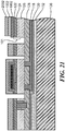
- FIG. 1 is a schematic diagram showing cross-sectional and top views of an exemplary piezoelectric gyroscope 100 in accordance with an example of the present invention. For convenience, these two views are not drawn to the same scale.
- the main components of this exemplary piezoelectric gyroscope are a disk 105 of piezoelectric material, a disk 104 underlying the disk 105 and representing a bottom electrode, and a top electrode 102 overlying a portion of the disk 105.
- the disk 104 is an N++ silicon (e.g., doped silicon) material
- the disk 105 is aluminum nitride (AlN)
- the top electrode 102 is molybdenum (Moly), although other appropriate materials may be used in various alternative embodiments.
- the disk 104 is anchored to an underlying substrate within a hub region 114.
- the top electrode 102 and the bottom electrode 104 must be electrically isolated from one another, which is accomplished in this example by an isolation trench 112 formed through the disk 104.
- the isolation trench 112 is a nitride/oxide (Nit/Ox) lined poly silicon-filled trench, although other appropriate materials may be used in various alternative embodiments.
- the isolated portion 108 of the disk 104 created by the isolation trench 112 provides an anchor and electrical contact to the top electrode 102.
- Electrical contacts (runners) 109 and 110 to the top and bottom electrodes, respectively, are formed from the poly silicon layer 118.
- a bond pad 106 providing for electrical connection to the top electrode via the contact/runner 109 is shown.
- a bond pad 116 for making an electrical connection to the silicon substrate 120 is shown in the cross-sectional view.
- a bond pad providing for electrical connection to the bottom electrode via the contact/runner 110 is not shown, although this bond pad would be formed substantially as the bond pad 106 is formed, i.e., a bond pad formed on top of a Moly 122, AlN 124, N++ 126, oxide 128 stack.
- the bond pads are typically metal.
- the piezoelectric disk 105 can be made to resonate by placing alternating electrical signals on the top and bottom electrodes 102 and 104, and external movements of the gyroscope can be sensed via various sense electrodes that, for convenience, are not shown. Such sense electrodes may be configured to sense in-plane and/or out-of-plane movements of the disk 105 caused by external movements of the gyroscope.
- An etch release hole 150 is discussed more fully below.
- FIG. 1 An exemplary fabrication process for fabricating the exemplary piezoelectric gyroscope 100 is now described with reference to FIGs. 2-21 .
- this exemplary fabrication process starts building the exemplary piezoelectric gyroscope 100 upside-down from what is shown in FIG. 1 , i.e., fabricating the layers starting with N++ 126 through oxide 132, bonding a silicon wafer 136 onto the oxide layer 132 (e.g., direct silicon bonding or fusion bonding), and then flipping the device over to fabricate the AlN 124 structures, the Moly 122 structures, and bond pads (e.g., 106, 116), e.g., using the silicon wafer 136 as a handling wafer for such "back-side” processing.
- bond pad 116 and its associated poly silicon 134 via to the silicon substrate 136 are not shown, although it will be apparent to persons of ordinary skill in the art how such structures can be formed within the described fabrication process.
- a layer of oxide 127 is deposited onto a substrate of N++ 126.
- the N++ 126 is approximately 750 microns and the oxide 127 is deposited to a thickness of approximately 1 micron.
- an alignment trench 302 is formed by etching through the oxide 127 layer into the N++ 126 layer.
- the alignment trench 302 is approximately 25 microns deep for a 20 micron device layer. In essence, all masking operations in later fabrication steps are aligned using the alignment trench 302 such that the alignment trench 302 represents a fixed reference for masking/etching operations.
- additional oxide 402 is deposited to line the alignment trench 302.
- the lined trench 302 is then filled with polysilicon 404, specifically by depositing polysilicon sufficiently to fill the lined trench 302, which also deposits polysilicon on the surface of the oxide 127, and then blanket etching the polysilicon to remove the polysilicon on the surface of the oxide 127 layer to leave the lined trench filled with polysilicon 404.
- the lined, filled trench 302 is used as an alignment key in later fabrication steps.
- the oxide 127 is removed, and a new oxide layer 128 is deposited and polished through a chemical mechanical polish (CMP) operation.
- CMP chemical mechanical polish
- the additional oxide 128 is formed to a thickness of approximately 2 microns plus or minus 0.2 microns.
- trenches for the various polysilicon layer 118 "vias" are etched through the oxide 128 layer, specifically by masking and etching through the oxide 128 layer.
- trenches 702 are formed for the portion of the electrical contact 109 underneath the bond pad 106
- trench 704 is formed for the portion of the electrical contact 109 underneath the isolated portion 108
- trench 706 is formed for the portion of the electrical contact 110 for making electrical connection to the bottom electrode 104.
- polysilicon layer 118 is deposited and patterned, specifically by masking and etching, in order to fill the trenches 702, 704, 706 and form the electrical contacts 109 and 110. Deposition of the polysilicon 118 fills the trenches and places a layer of polysilicon onto the oxide 128. This layer of polysilicon is then patterned, specifically by masking and etching.
- a layer of low-stress nitride is deposited over the exposed oxide 128 and polysilicon 118 as an etch stop layer for later fabrication steps.
- an oxide 132 layer is formed on the LSN 130 layer, specifically by deposition and CMP of the oxide 132.
- a silicon wafer substrate 136 is direct wafer bonded to the oxide 132 layer. This silicon wafer substrate 136 is used as a handling wafer for "back-side" processing in which the device is flipped over and fabrication steps are performed on the N++ 126 side of the device.
- FIG. 11 shows the device flipped over for back-side processing.
- the N++ layer is ground and polished to the desired device layer thickness (in this example, approximately 20 microns), which also exposes the lined 402, filled 404 alignment trench 302 for use as an alignment key in later fabrication steps.
- a temporary thermal oxide layer 1302 is formed on the N++ 126 layer, and then isolation trench 112 is formed by patterning by masking and etching through the oxide 1302 and N++ 126 layers to the oxide 128 layer.
- the isolation trench 112 is lined and filled in later fabrication processes. As discussed above, the isolated portion of the disk 104 (which is formed of N++ 126 material) created by the isolation trench 112 provides an anchor and electrical contact 108 to the top electrode 102.
- the isolation trench 112 is lined, specifically by depositing a layer of nitride 1401 over the oxide 1302. This nitride layer lines the trench 112. Then, polysilicon 1402 is deposited to fill the lined isolation trench 112 and form a polysilicon 1402 layer on the nitride 1401 layer.
- a series of processes are performed to remove the polysilicon 1402 layer, the surface nitride 1401 layer, and the temporary thermal oxide 1302 layer.
- a blanket polysilicon etch process is used to remove the polysilicon 1402 layer, with the nitride 1401 layer acting as an etch stop layer.
- a hot phosphoric acid etch is performed to remove the surface nitride 1401 layer, and then a timed wet oxide etch is performed to remove the temporary thermal oxide 1302 layer.
- a layer of piezoelectric AlN 124 is deposited and patterned by masking and etching to define contact holes 1502 and 1504. Then, a layer of Moly 122 is deposited.
- metal bond pads including bond pad 106 (shown), bond pad 116 (not shown), and a bond pad for the electrical contact 110 (not shown) are formed on the Moly 122 layer. This involves depositing metal (in this example, aluminum) and then patterning the metal by masking and etching to form the bond pads and optionally a bond ring (not shown) surrounding the resonator if the device is to be capped.
- an oxide hard mask 1802 is deposited, the oxide hard mask 1802 is patterned by masking and etching to expose portions of the Moly 122 to be etched including the portion represented at location 101 in FIGs. 1 and 21 (i.e., any Moly 122 not being etched is covered with oxide 1802), and the Moly 122 is etched using the oxide hard mask 1802 to form the Moly 122 top electrode 102 and other Moly 122 structures.
- various etch release holes 150 may be formed through the Moly 122 top electrode 102 to facilitate release of the piezoelectric disk in later fabrication steps.
- FIG. 18 (which shows a magnified view of a portion of the structures shown in FIG. 17 ), a second oxide hard mask 1902 is deposited.
- a photoresist material layer 2002 is deposited and patterned to expose portions of the second oxide hard mask 1902 that will be etched. This step may expose a portion of the second oxide hard mask 1902 covering any etch release holes 150 formed through the Moly 122 top electrode 102 as discussed above with reference to FIG. 17 (for convenience, this is not shown in FIG. 19 ).
- the thinner second oxide hard mask 1902 is dry etched via an oxide timed etch process to expose portions of the AlN 124 layer that will be etched, including the portion represented at location 101 in FIGs. 1 and 21 and also including any etch release holes 150 formed through the Moly 122 top electrode 102 as discussed above with reference to FIGs. 17 and 19 (for convenience, this is not shown in FIG. 20 ).
- the combination of the first oxide hard mask 1802 and the thinner second oxide hard mask 1902 that is fully etched to expose the AlN 124 layer without fully etching the first oxide hard mask 1802 provides the self-alignment between the edge of the top moly electrode 122 and the piezoelectric layer 124 and the bottom electrode 126.
- AlN and silicon etch operations are performed to etch through the AlN 124 and N++ 126 layers where those layers were exposed through the oxide hard masks.
- these etch operations result in self-alignment of the Moly 122 top electrode 102, the AlN 124 disk 105, and the N++ 126 bottom electrode 104, as represented at location 101 in FIGs. 1 and 21 .
- These etch operations also remove portions of the AlN 124 and N++ 126 layers at any etch release holes 150 formed through the second oxide hard mask 1902 and Moly 122 top electrode 102 (for convenience, this is not shown in FIG. 21 ).
- etch operations also expose portions of the oxide 128 layer (including portions of the oxide 128 layer exposed through any etch release holes 150 formed through the Moly 122, AlN 124, and N++ 126 layers as discussed above), particularly to allow for "release" of the piezoelectric disk. It should be noted that, by running the electrical connections 109 and 110 underneath the resonator, electrical connections can be made to both the top electrode 102 and the bottom electrode 104 without having to cross the open trench that surrounds the resonator and without having to cross a bond ring if present.
- the residual photoresist 2002, oxide 1902, and oxide 1802 are removed using appropriate etching operations.
- the oxide 128 layer is then dry etched (e.g., using vapor HF etchant) through exposed openings (including any etch release holes 150) to remove portions of the oxide 128 layer underlying the bottom electrode 104 and elsewhere. Removing portions of the oxide 128 layer underlying the bottom electrode 104 effectively "releases" the piezoelectric disk. Any etch release holes 150 also facilitate removal of the oxide 128 layer by providing additional locations for the dry etchant to reach the oxide 128 layer.
- the LSN 130 layer acts as an etch-stop layer to prevent etching beyond areas where the oxide 128 layer touches the LSN 130 layer.
- the various masking steps discussed above typically involve use of a photo mask, i.e., deposition of a photoresist material, exposing portions of the photoresist material using a mask to define areas to be etched, removing photoresist material from the areas to be etched, etching one or more underlying material layers through the removed areas of photoresist material, and then removing the residual photoresist material.
- a photo mask i.e., deposition of a photoresist material
- exposing portions of the photoresist material using a mask to define areas to be etched to define areas to be etched
- removing photoresist material from the areas to be etched etching one or more underlying material layers through the removed areas of photoresist material, and then removing the residual photoresist material.
- Using the alignment trench 302 as a reference for masking helps to align the various masking and etching steps to avoid or reduce the above-mentioned issues with photo mask misalignment.
- patterning may include various deposition and etching steps, etc.
- piezoelectric MEMS gyroscope and a piezoelectric element that is a disk
- the present invention is not limited to piezoelectric gyroscopes or piezoelectric disk structures. Rather, examples of the present invention can apply more generally to other types of piezoelectric MEMS devices and/or to piezoelectric MEMS gyroscopes having piezoelectric elements of other shapes.
- the present invention is not limited to fabrication of piezoelectric elements such as resonators or proof masses for a gyroscope or inertial sensor. Rather, examples of the present invention can apply more generally to other types of piezoelectric elements in MEMS device, such as, for example, piezoelectric transducers described in U.S. Patent Application Publication No. 2010/0058861 .
Description
- The present invention relates to fabrication of piezoelectric MEMS devices.
- In a vibratory MEMS gyroscope, a mass is driven to resonate, e.g., in a translational, rotational, flexural, or bulk acoustic mode, by a set of drive electrodes, and motion is detected through a set of sense electrodes. Gyroscope errors and performance is determined, in part, by the matching and optimum alignment of the drive and sense electrodes with respect to the mode shape of operation. Photo mask misalignment is one source of these errors if more than one photo mask is used to define the critical layers of the MEMS gyroscope structures.
- United States patent application no.
11/761,767 2007/0284971 discloses an electronic device including a lower electrode; a first piezoelectric film provided on the lower electrode; and an upper electrode provided on the first piezoelectric film. At least one of the lower electrode and the upper electrode is made of an alloy composed primarily of aluminum and doped with at least one element selected from the group consisting of Ni, Co, V, Ta, Mo, W, Ti, Y, and Nd. Alternatively, an electronic device includes: a support substrate; a lower electrode provided on the support substrate; a first piezoelectric film provided on the lower electrode; and an upper electrode provided on the first piezoelectric film. The lower electrode is made of an alloy composed primarily of aluminum and doped with at least one element selected from the group consisting of Ni, Co, V, Ta, Mo, W, Ti, Y, and Nd. - United States patent application no.
11/300,585 2007/0069342 discloses a first electrode formed on a semiconductor substrate. A second electrode is formed separately at a predetermined interval from the first electrode, and has at least one opening. An actuator layer is connected to the second electrode, and drives the second electrode. - Japanese patent application no.
2008-323650 2010-147285 - A first aspect of the invention provides a device in accordance with claim 1.
- A second aspect of the invention provides a method of fabricating a piezoelectric device in accordance with claim 9.
- In a first example there is provided a piezoelectric device comprising a top electrode; a piezoelectric element under the top electrode and self-aligned with the top electrode; and a bottom electrode under the piezoelectric element and self-aligned with the top electrode and the piezoelectric element.
- In various alternative examples, the piezoelectric element may be an aluminum nitride piezoelectric element. The top electrode may be a molybdenum electrode. The bottom electrode may be an N++ electrode such as a doped polysilicon electrode. The piezoelectric device may be a bulk acoustic wave piezoelectric gyroscope.
- In certain other examples, the bottom electrode may be formed from a bottom electrode material layer, and the piezoelectric gyroscope may further comprise an isolation trench within the bottom electrode material layer, the isolation trench forming an electrically-isolated anchor in the bottom electrode material layer to which the top electrode is coupled.
- The device may further comprise a first electrical contact to the bottom electrode and a second electrical contact to the electrically-isolated anchor for making an electrical connection to the top electrode, wherein the first and second electrical contacts run underneath the bottom electrode material layer and include conductive vias to the bottom electrode material layer. The first and second electrical contacts may be polysilicon electrical contacts. The device may further comprise a first metallic bond pad electrically coupled to the first electrical contact and a second metallic bond pad electrically coupled to the second electrical contact, wherein the top electrode is formed from a top electrode material layer, and wherein the first and second metallic bond pads are at a metallic material layer above the top electrode material layer.
- In a second example of the invention there is provided a method of fabricating a piezoelectric device comprising forming a piezoelectric material layer on a bottom electrode material layer; forming a top electrode on the piezoelectric material layer; and etching the piezoelectric material layer and the bottom electrode material layer to produce a piezoelectric element and a bottom electrode self-aligned with the top electrode.
- In various alternative examples, forming the piezoelectric material layer may involve forming an aluminum nitride material layer. Forming the top electrode may involve forming a molybdenum material layer; patterning the molybdenum material layer; and etching the molybdenum material layer to form a molybdenum electrode. The bottom electrode material layer may be an N++ material layer such as a doped polysilicon material layer. Etching the piezoelectric material layer and the bottom electrode material layer may involve forming an oxide hard mask; patterning the oxide hard mask to expose portions of the piezoelectric material layer to be etched; etching the exposed portions of the piezoelectric material layer to expose portions of the bottom electrode material layer to be etched; and etching the exposed portions of the bottom electrode material layer.
- In certain other examples, the method may further involve forming an isolation trench within the bottom electrode material layer, the isolation trench forming an electrically- isolated isolated anchor in the bottom electrode material layer to which the top electrode is coupled. The method may further involve forming a first electrical contact to the bottom electrode and forming a second electrical contact to the electrically-isolated anchor for making an electrical connection to the top electrode, wherein the first and second electrical contacts run underneath the bottom electrode material layer and include conductive vias to the bottom electrode material layer. Forming the first and second electrical contacts may involve forming polysilicon electrical contacts. The method may further involve forming a first metallic bond pad electrically coupled to the first electrical contact and forming a second metallic bond pad electrically coupled to the second electrical contact, wherein the top electrode is formed from a top electrode material layer, and wherein the first and second metallic bond pads are at a metallic material layer above the top electrode material layer.
- The foregoing features of examples will be more readily understood by reference to the following detailed description, taken with reference to the accompanying drawings, in which:
-
FIG. 1 is a schematic diagram showing cross-sectional and top views of an exemplarypiezoelectric gyroscope 100 in accordance with an example of the present invention; and -
FIGs. 2-21 are schematic diagrams used to represent various fabrication process steps in fabricating the exemplary piezoelectric gyroscope in accordance with an example of the present invention. - It should be noted that the foregoing figures and the elements depicted therein are not necessarily drawn to consistent scale or to any scale. Unless the context otherwise suggests, like elements are indicated by like numerals.
- Examples of the present invention use a single photo mask to define the three critical layers for the piezoelectric MEMS device, specifically the top electrode layer, the piezoelectric material layer, and the bottom electrode layer. Using a single photo mask removes the misalignment source caused by using multiple photo masks.
- Furthermore, in certain examples, all electrical interconnects use underpass interconnect. This simplifies the process for defining the device electrodes and the process sequence for achieving self-alignment between the piezoelectric element and the top and bottom electrodes. This self-alignment is achieved by using an oxide hard mask to etch the critical region of the top electrode, the piezoelectric material, and the bottom electrode with one mask and different etch chemistries depending on the layer being etched.
-
FIG. 1 is a schematic diagram showing cross-sectional and top views of an exemplarypiezoelectric gyroscope 100 in accordance with an example of the present invention. For convenience, these two views are not drawn to the same scale. The main components of this exemplary piezoelectric gyroscope are adisk 105 of piezoelectric material, adisk 104 underlying thedisk 105 and representing a bottom electrode, and atop electrode 102 overlying a portion of thedisk 105. In this example, thedisk 104 is an N++ silicon (e.g., doped silicon) material, thedisk 105 is aluminum nitride (AlN), and thetop electrode 102 is molybdenum (Moly), although other appropriate materials may be used in various alternative embodiments. Thedisk 104 is anchored to an underlying substrate within ahub region 114. In order to provide electrical connections to both thetop electrode 102 and thebottom electrode 104 via various runners formed at apolysilicon layer 118 underlying thedisk 104, thetop electrode 102 and thebottom electrode 104 must be electrically isolated from one another, which is accomplished in this example by anisolation trench 112 formed through thedisk 104. In this example, theisolation trench 112 is a nitride/oxide (Nit/Ox) lined poly silicon-filled trench, although other appropriate materials may be used in various alternative embodiments. Theisolated portion 108 of thedisk 104 created by theisolation trench 112 provides an anchor and electrical contact to thetop electrode 102. Electrical contacts (runners) 109 and 110 to the top and bottom electrodes, respectively, are formed from thepoly silicon layer 118. Abond pad 106 providing for electrical connection to the top electrode via the contact/runner 109 is shown. Abond pad 116 for making an electrical connection to thesilicon substrate 120 is shown in the cross-sectional view. For convenience, a bond pad providing for electrical connection to the bottom electrode via the contact/runner 110 is not shown, although this bond pad would be formed substantially as thebond pad 106 is formed, i.e., a bond pad formed on top of aMoly 122, AlN 124,N++ 126,oxide 128 stack. The bond pads are typically metal. Using principles known in the art, thepiezoelectric disk 105 can be made to resonate by placing alternating electrical signals on the top andbottom electrodes disk 105 caused by external movements of the gyroscope. Anetch release hole 150 is discussed more fully below. - An exemplary fabrication process for fabricating the exemplary
piezoelectric gyroscope 100 is now described with reference toFIGs. 2-21 . In essence, this exemplary fabrication process starts building the exemplarypiezoelectric gyroscope 100 upside-down from what is shown inFIG. 1 , i.e., fabricating the layers starting withN++ 126 throughoxide 132, bonding asilicon wafer 136 onto the oxide layer 132 (e.g., direct silicon bonding or fusion bonding), and then flipping the device over to fabricate theAlN 124 structures, theMoly 122 structures, and bond pads (e.g., 106, 116), e.g., using thesilicon wafer 136 as a handling wafer for such "back-side" processing. Purely for convenience, fabrication steps involved with formation of thebond pad 116 and its associatedpoly silicon 134 via to thesilicon substrate 136 are not shown, although it will be apparent to persons of ordinary skill in the art how such structures can be formed within the described fabrication process. - In
FIG. 2 , a layer ofoxide 127 is deposited onto a substrate ofN++ 126. In this example, theN++ 126 is approximately 750 microns and theoxide 127 is deposited to a thickness of approximately 1 micron. - In
FIG. 3 , analignment trench 302 is formed by etching through theoxide 127 layer into theN++ 126 layer. In this example, thealignment trench 302 is approximately 25 microns deep for a 20 micron device layer. In essence, all masking operations in later fabrication steps are aligned using thealignment trench 302 such that thealignment trench 302 represents a fixed reference for masking/etching operations. - In
FIG. 4 ,additional oxide 402 is deposited to line thealignment trench 302. The linedtrench 302 is then filled withpolysilicon 404, specifically by depositing polysilicon sufficiently to fill the linedtrench 302, which also deposits polysilicon on the surface of theoxide 127, and then blanket etching the polysilicon to remove the polysilicon on the surface of theoxide 127 layer to leave the lined trench filled withpolysilicon 404. The lined, filledtrench 302 is used as an alignment key in later fabrication steps. - In
FIG. 5 , theoxide 127 is removed, and anew oxide layer 128 is deposited and polished through a chemical mechanical polish (CMP) operation. In this example, theadditional oxide 128 is formed to a thickness of approximately 2 microns plus or minus 0.2 microns. - In
FIG. 6 , trenches for thevarious polysilicon layer 118 "vias" are etched through theoxide 128 layer, specifically by masking and etching through theoxide 128 layer. Here,trenches 702 are formed for the portion of theelectrical contact 109 underneath thebond pad 106,trench 704 is formed for the portion of theelectrical contact 109 underneath theisolated portion 108, andtrench 706 is formed for the portion of theelectrical contact 110 for making electrical connection to thebottom electrode 104. - In
FIG. 7 ,polysilicon layer 118 is deposited and patterned, specifically by masking and etching, in order to fill thetrenches electrical contacts polysilicon 118 fills the trenches and places a layer of polysilicon onto theoxide 128. This layer of polysilicon is then patterned, specifically by masking and etching. - In
FIG. 8 , a layer of low-stress nitride (LSN) is deposited over the exposedoxide 128 andpolysilicon 118 as an etch stop layer for later fabrication steps. - In
FIG. 9 , anoxide 132 layer is formed on theLSN 130 layer, specifically by deposition and CMP of theoxide 132. - In
FIG. 10 , asilicon wafer substrate 136 is direct wafer bonded to theoxide 132 layer. Thissilicon wafer substrate 136 is used as a handling wafer for "back-side" processing in which the device is flipped over and fabrication steps are performed on theN++ 126 side of the device. -
FIG. 11 shows the device flipped over for back-side processing. InFIG. 11 , the N++ layer is ground and polished to the desired device layer thickness (in this example, approximately 20 microns), which also exposes the lined 402, filled 404alignment trench 302 for use as an alignment key in later fabrication steps. - In
FIG. 12 , a temporarythermal oxide layer 1302 is formed on theN++ 126 layer, and thenisolation trench 112 is formed by patterning by masking and etching through theoxide 1302 and N++ 126 layers to theoxide 128 layer. Theisolation trench 112 is lined and filled in later fabrication processes. As discussed above, the isolated portion of the disk 104 (which is formed ofN++ 126 material) created by theisolation trench 112 provides an anchor andelectrical contact 108 to thetop electrode 102. - In
FIG. 13 , theisolation trench 112 is lined, specifically by depositing a layer ofnitride 1401 over theoxide 1302. This nitride layer lines thetrench 112. Then,polysilicon 1402 is deposited to fill the linedisolation trench 112 and form apolysilicon 1402 layer on thenitride 1401 layer. - In
FIG. 14 , a series of processes are performed to remove thepolysilicon 1402 layer, thesurface nitride 1401 layer, and the temporarythermal oxide 1302 layer. Specifically, a blanket polysilicon etch process is used to remove thepolysilicon 1402 layer, with thenitride 1401 layer acting as an etch stop layer. Then, a hot phosphoric acid etch is performed to remove thesurface nitride 1401 layer, and then a timed wet oxide etch is performed to remove the temporarythermal oxide 1302 layer. - In
FIG. 15 , a layer ofpiezoelectric AlN 124 is deposited and patterned by masking and etching to definecontact holes Moly 122 is deposited. - In
FIG. 16 , metal bond pads including bond pad 106 (shown), bond pad 116 (not shown), and a bond pad for the electrical contact 110 (not shown) are formed on theMoly 122 layer. This involves depositing metal (in this example, aluminum) and then patterning the metal by masking and etching to form the bond pads and optionally a bond ring (not shown) surrounding the resonator if the device is to be capped. - In
FIG. 17 , an oxidehard mask 1802 is deposited, the oxidehard mask 1802 is patterned by masking and etching to expose portions of theMoly 122 to be etched including the portion represented atlocation 101 inFIGs. 1 and21 (i.e., anyMoly 122 not being etched is covered with oxide 1802), and theMoly 122 is etched using the oxidehard mask 1802 to form theMoly 122top electrode 102 andother Moly 122 structures. It should be noted that various etch release holes 150 (not shown inFIG. 17 ) may be formed through theMoly 122top electrode 102 to facilitate release of the piezoelectric disk in later fabrication steps. - In
FIG. 18 (which shows a magnified view of a portion of the structures shown inFIG. 17 ), a second oxidehard mask 1902 is deposited. - In
FIG. 19 , aphotoresist material layer 2002 is deposited and patterned to expose portions of the second oxidehard mask 1902 that will be etched. This step may expose a portion of the second oxidehard mask 1902 covering any etch release holes 150 formed through theMoly 122top electrode 102 as discussed above with reference toFIG. 17 (for convenience, this is not shown inFIG. 19 ). - In
FIG. 20 , the thinner second oxidehard mask 1902 is dry etched via an oxide timed etch process to expose portions of theAlN 124 layer that will be etched, including the portion represented atlocation 101 inFIGs. 1 and21 and also including any etch release holes 150 formed through theMoly 122top electrode 102 as discussed above with reference toFIGs. 17 and19 (for convenience, this is not shown inFIG. 20 ). As shown and described with reference toFIG. 21 , the combination of the first oxidehard mask 1802 and the thinner second oxidehard mask 1902 that is fully etched to expose theAlN 124 layer without fully etching the first oxidehard mask 1802 provides the self-alignment between the edge of thetop moly electrode 122 and thepiezoelectric layer 124 and thebottom electrode 126. - In
FIG. 21 , AlN and silicon etch operations are performed to etch through theAlN 124 andN++ 126 layers where those layers were exposed through the oxide hard masks. Among other things, these etch operations result in self-alignment of theMoly 122top electrode 102, theAlN 124disk 105, and theN++ 126bottom electrode 104, as represented atlocation 101 inFIGs. 1 and21 . These etch operations also remove portions of theAlN 124 andN++ 126 layers at any etch release holes 150 formed through the second oxidehard mask 1902 andMoly 122 top electrode 102 (for convenience, this is not shown inFIG. 21 ). These etch operations also expose portions of theoxide 128 layer (including portions of theoxide 128 layer exposed through any etch release holes 150 formed through theMoly 122,AlN 124, andN++ 126 layers as discussed above), particularly to allow for "release" of the piezoelectric disk. It should be noted that, by running theelectrical connections top electrode 102 and thebottom electrode 104 without having to cross the open trench that surrounds the resonator and without having to cross a bond ring if present. - In subsequent steps leading to the
final device configuration 100 shown inFIG. 1 , theresidual photoresist 2002,oxide 1902, andoxide 1802 are removed using appropriate etching operations. Theoxide 128 layer is then dry etched (e.g., using vapor HF etchant) through exposed openings (including any etch release holes 150) to remove portions of theoxide 128 layer underlying thebottom electrode 104 and elsewhere. Removing portions of theoxide 128 layer underlying thebottom electrode 104 effectively "releases" the piezoelectric disk. Any etch release holes 150 also facilitate removal of theoxide 128 layer by providing additional locations for the dry etchant to reach theoxide 128 layer. TheLSN 130 layer acts as an etch-stop layer to prevent etching beyond areas where theoxide 128 layer touches theLSN 130 layer. - The various masking steps discussed above typically involve use of a photo mask, i.e., deposition of a photoresist material, exposing portions of the photoresist material using a mask to define areas to be etched, removing photoresist material from the areas to be etched, etching one or more underlying material layers through the removed areas of photoresist material, and then removing the residual photoresist material. Using the
alignment trench 302 as a reference for masking helps to align the various masking and etching steps to avoid or reduce the above-mentioned issues with photo mask misalignment. - It should be noted that the exemplary processes discussed above may involve (and often do involve) additional and/or alternate steps that are omitted for convenience. For example, patterning may include various deposition and etching steps, etc.
- While examples, of the invention are described with reference to a piezoelectric MEMS gyroscope and a piezoelectric element that is a disk, it should be noted that the present invention is not limited to piezoelectric gyroscopes or piezoelectric disk structures. Rather, examples of the present invention can apply more generally to other types of piezoelectric MEMS devices and/or to piezoelectric MEMS gyroscopes having piezoelectric elements of other shapes. Furthermore, the present invention is not limited to fabrication of piezoelectric elements such as resonators or proof masses for a gyroscope or inertial sensor. Rather, examples of the present invention can apply more generally to other types of piezoelectric elements in MEMS device, such as, for example, piezoelectric transducers described in
U.S. Patent Application Publication No. 2010/0058861 . - The examples of the invention described above are intended to be merely exemplary; numerous variations and modifications will be apparent to those skilled in the art. All such All such variations and modifications of the examples are intended to be within the scope of the present invention as defined in any appended claims.
Claims (15)
- A piezoelectric device (100) comprising:a top electrode material layer (122);a piezoelectric material layer (124) under the top electrode material layer;a bottom electrode material layer (126) under the piezoelectric material layer; andcharacterized by:a first oxide hard mask layer (1802) overlying the top electrode material layer, the first oxide hard mask layer including an etch pattern that exposes a portion of the piezoelectric material layer through an etched portion of the top electrode material layer; anda second oxide hard mask layer (1902) overlying the first oxide hard mask layer, wherein the second oxide hard mask layer is thinner than the first oxide hard mask layer, and wherein the second oxide hard mask layer includes an etch pattern that exposes the portion of the piezoelectric material layer through the etch pattern of the first oxide hard mask layer and the etched portion of the top electrode material layer.
- A device according to claim 1, wherein at least one of the following apply:a) the piezoelectric material layer is an aluminum nitride material layer;b) the top electrode material layer is a molybdenum material layer;c) the bottom electrode material layer is an N++ material layer;d) the bottom electrode material layer is a doped silicon material layer.
- A device according to claim 1 or 2, wherein the device further comprises an isolation trench (112) within the bottom electrode material layer, the isolation trench forming an electrically-isolated anchor (108) in the bottom electrode material layer to which the top electrode material layer is coupled.
- A device according to claim 3, further comprising:a first electrical contact (110) to the bottom electrode material layer; anda second electrical contact (109) to the electrically-isolated anchor for making an electrical connection to the top electrode material layer, wherein the first and second electrical contacts run underneath the bottom electrode material layer and include conductive vias to the bottom electrode material layer.
- A device according to claim 4, wherein the first and second electrical contacts are polysilicon electrical contacts.
- A device according to claim 4 or 5, further comprising:a first metallic bond pad electrically coupled to the first electrical contact; anda second metallic bond pad (106) electrically coupled to the second electrical contact, wherein the first and second metallic bond pads are at a metallic material layer above the top electrode material layer.
- A device according to any preceding claim, wherein the device is a bulk acoustic wave piezoelectric gyroscope.
- A device according to any preceding claim, wherein the etch patterns of the first and second oxide hard mask layers are arranged so that the top electrode material layer, the piezoelectric material layer and the bottom electrode material layer are etched to produce a piezoelectric element and a bottom electrode self-aligned with a top electrode such that an edge of the top electrode is vertically aligned with an edge of the piezoelectric element and an edge of the bottom electrode.
- A method of fabricating a piezoelectric device, the method comprising:forming a piezoelectric material layer on a bottom electrode material layer;forming a top electrode material layer on the piezoelectric material layer; andcharacterized in that:
etching the top electrode material layer, the piezoelectric material layer and the bottom electrode material layer to produce a piezoelectric element, a bottom electrode and a top electrode,etching the top electrode material layer, the piezoelectric material layer and the bottom electrode material layer comprises:forming a first oxide hard mask layer overlaying the top electrode material layer;patterning the first oxide hard mask layer to expose portions of the piezoelectric material layer to be etched through an etched portion of the top electrode material layer;forming a second oxide hard mask layer overlaying the first oxide hard mask layer, wherein the second oxide hard mask layer is thinner than the first oxide hard mask layer;patterning the second oxide hard mask layer to expose the portion of the piezoelectric material layer to be etched though the etch pattern of the first oxide hard mask layer and the etched portion of the top electrode material layer;etching the exposed portions of the piezoelectric material layer to expose portions of the bottom electrode material layer to be etched; andetching the exposed portions of the bottom electrode material layer. - A method according to claim 9, wherein at least one of the following apply:a) forming the piezoelectric material layer comprises forming an aluminum nitride material layer;b) forming the top electrode material layer comprises forming a molybdenum material layer;c) wherein the bottom electrode material layer is an N++ material layer;d) wherein the bottom electrode material layer is a doped silicon material layer;e) the method comprises using a single photo mask to define the edge of the top electrode material layer, the piezoelectric material layer and the bottom electrode material layer.
- A method according to any of claims 9 to 10, further comprising:forming an isolation trench within the bottom electrode material layer, the isolation trench forming an electrically-isolated anchor in the bottom electrode material layer to which the top electrode is coupled.
- A method according to claim 11, further comprising:forming a first electrical contact to the bottom electrode; andforming a second electrical contact to the electrically-isolated anchor for making an electrical connection to the top electrode, wherein the first and second electrical contacts run underneath the bottom electrode material layer and include conductive vias to the bottom electrode material layer.
- A method according to claim 12, wherein forming the first and second electrical contacts comprises forming polysilicon electrical contacts.
- A method according to claim 12 or 13, further comprising:forming a first metallic bond pad electrically coupled to the first electrical contact; andforming a second metallic bond pad electrically coupled to the second electrical contact, wherein the top electrode is formed from a top electrode material layer, and wherein the first and second metallic bond pads are at a metallic material layer above the top electrode material layer.
- A method according to any one of claims 9 to 14, wherein the top electrode material layer, the piezoelectric material layer and the bottom electrode material layer are etched such that an edge of the top electrode is vertically aligned with an edge of the piezoelectric element and an edge of the bottom electrode.
Applications Claiming Priority (1)
| Application Number | Priority Date | Filing Date | Title |
|---|---|---|---|
| US14/515,929 US9917243B2 (en) | 2014-10-16 | 2014-10-16 | Method of fabricating piezoelectric MEMS devices |
Publications (2)
| Publication Number | Publication Date |
|---|---|
| EP3009793A1 EP3009793A1 (en) | 2016-04-20 |
| EP3009793B1 true EP3009793B1 (en) | 2017-09-27 |
Family
ID=54324883
Family Applications (1)
| Application Number | Title | Priority Date | Filing Date |
|---|---|---|---|
| EP15189732.9A Active EP3009793B1 (en) | 2014-10-16 | 2015-10-14 | Method of fabricating piezoelectric mems device |
Country Status (2)
| Country | Link |
|---|---|
| US (1) | US9917243B2 (en) |
| EP (1) | EP3009793B1 (en) |
Families Citing this family (2)
| Publication number | Priority date | Publication date | Assignee | Title |
|---|---|---|---|---|
| US9862592B2 (en) | 2015-03-13 | 2018-01-09 | Taiwan Semiconductor Manufacturing Co., Ltd. | MEMS transducer and method for manufacturing the same |
| US11527700B2 (en) | 2019-12-20 | 2022-12-13 | Vanguard International Semiconductor Singapore Pte. Ltd. | Microphone device with single crystal piezoelectric film and method of forming the same |
Family Cites Families (28)
| Publication number | Priority date | Publication date | Assignee | Title |
|---|---|---|---|---|
| GB8404668D0 (en) | 1984-02-22 | 1984-03-28 | Burdess J S | Gyroscopic devices |
| US5767405A (en) | 1992-04-07 | 1998-06-16 | The Charles Stark Draper Laboratory, Inc. | Comb-drive micromechanical tuning fork gyroscope with piezoelectric readout |
| US5616864A (en) | 1995-02-22 | 1997-04-01 | Delco Electronics Corp. | Method and apparatus for compensation of micromachined sensors |
| JPH09116250A (en) | 1995-10-24 | 1997-05-02 | Tokin Corp | Piezoelectric transformer retaining member |
| JPH10115526A (en) | 1996-10-15 | 1998-05-06 | Ngk Insulators Ltd | Vibration gyro sensor and manufacture of vibration gyro sensor |
| US6209393B1 (en) | 1996-10-29 | 2001-04-03 | Mitsui Chemicals Inc. | Vibration gyroscope |
| JPH10232132A (en) | 1997-02-20 | 1998-09-02 | Murata Mfg Co Ltd | Vibration gyro |
| US6151964A (en) | 1998-05-25 | 2000-11-28 | Citizen Watch Co., Ltd. | Angular velocity sensing device |
| US6438242B1 (en) | 1999-09-07 | 2002-08-20 | The United States Of America As Represented By The Secretary Of The Navy | Acoustic transducer panel |
| US6492222B1 (en) * | 1999-12-22 | 2002-12-10 | Texas Instruments Incorporated | Method of dry etching PZT capacitor stack to form high-density ferroelectric memory devices |
| JP3642026B2 (en) | 2001-01-12 | 2005-04-27 | 株式会社村田製作所 | Acceleration sensor and manufacturing method thereof |
| US6548943B2 (en) * | 2001-04-12 | 2003-04-15 | Nokia Mobile Phones Ltd. | Method of producing thin-film bulk acoustic wave devices |
| EP2325604B1 (en) | 2002-02-06 | 2013-04-24 | Analog Devices, Inc. | Micromachined gyroscope |
| US7089792B2 (en) | 2002-02-06 | 2006-08-15 | Analod Devices, Inc. | Micromachined apparatus utilizing box suspensions |
| US7382078B2 (en) * | 2002-07-30 | 2008-06-03 | Avago Technologies General Ip (Singapore) Pte. Ltd. | Electrostatic discharge protection of thin-film resonators |
| JP3953017B2 (en) | 2003-10-06 | 2007-08-01 | 株式会社村田製作所 | Piezoelectric vibrator for vibration gyro |
| US7043985B2 (en) | 2004-01-13 | 2006-05-16 | Georgia Tech Research Corporation | High-resolution in-plane tuning fork gyroscope and methods of fabrication |
| CN1985149B (en) | 2004-07-12 | 2010-11-03 | 住友精密工业株式会社 | Angular speed sensor |
| US7492241B2 (en) * | 2005-06-02 | 2009-02-17 | The Regents Of The University Of California | Contour-mode piezoelectric micromechanical resonators |
| JP4713990B2 (en) | 2005-09-13 | 2011-06-29 | 株式会社東芝 | Semiconductor device and manufacturing method thereof |
| US7345407B2 (en) | 2005-11-18 | 2008-03-18 | Adaptivenergy, Llc. | Human powered piezoelectric power generating device |
| US7420318B1 (en) | 2006-03-20 | 2008-09-02 | The United States Of America As Represented By The Secretary Of The Army | Lateral piezoelectric microelectromechanical system (MEMS) actuation and sensing device |
| JP2007335977A (en) | 2006-06-12 | 2007-12-27 | Toshiba Corp | Electron device |
| US8056413B2 (en) | 2007-09-11 | 2011-11-15 | Evigia Systems, Inc. | Sensor and sensing method utilizing symmetrical differential readout |
| US8278802B1 (en) * | 2008-04-24 | 2012-10-02 | Rf Micro Devices, Inc. | Planarized sacrificial layer for MEMS fabrication |
| US20100058861A1 (en) | 2008-09-11 | 2010-03-11 | Analog Devices, Inc. | Piezoelectric Transducers and Inertial Sensors using Piezoelectric Transducers |
| JP2010098518A (en) * | 2008-10-16 | 2010-04-30 | Rohm Co Ltd | Method of manufacturing mems sensor, and mems sensor |
| JP2010147285A (en) | 2008-12-19 | 2010-07-01 | Yamaha Corp | Mems, vibration gyroscope, and method of manufacturing mems |
-
2014
- 2014-10-16 US US14/515,929 patent/US9917243B2/en active Active
-
2015
- 2015-10-14 EP EP15189732.9A patent/EP3009793B1/en active Active
Non-Patent Citations (1)
| Title |
|---|
| None * |
Also Published As
| Publication number | Publication date |
|---|---|
| US9917243B2 (en) | 2018-03-13 |
| EP3009793A1 (en) | 2016-04-20 |
| US20160111625A1 (en) | 2016-04-21 |
Similar Documents
| Publication | Publication Date | Title |
|---|---|---|
| JP7297328B2 (en) | Packaging method and packaging structure for bulk acoustic wave resonator | |
| US10107830B2 (en) | Method of forming capacitive MEMS sensor devices | |
| CN102134054B (en) | Method for fabricating MEMS device | |
| CN110636422B (en) | Semiconductor device and method of forming the same | |
| CN103648967B (en) | The electrode that Out-of-plane spacer limits | |
| US8796845B2 (en) | Electronic device covered by multiple layers and method for manufacturing electronic device | |
| CN111151431B (en) | Piezoelectric micromechanical ultrasonic transducer and method for producing same | |
| US9908771B2 (en) | Inertial and pressure sensors on single chip | |
| TWI621242B (en) | Aluminum nitride (ain) devices with infrared absorption structural layer | |
| JP7218020B2 (en) | Packaging method and packaging structure for bulk acoustic wave resonator | |
| TW201034933A (en) | Microelectromechanical device with isolated microstructures and method of producing same | |
| JP4544140B2 (en) | MEMS element | |
| JP7134530B2 (en) | Packaging method and packaging structure for bulk acoustic wave resonator | |
| EP3009793B1 (en) | Method of fabricating piezoelectric mems device | |
| JP2000133616A (en) | Integrated device and manufacture thereof | |
| TWI652728B (en) | Epi-poly etch stop for out of plane spacer defined electrode | |
| US20110175177A1 (en) | Microelectromechanical system (mems) device and methods for fabricating the same | |
| US7531424B1 (en) | Vacuum wafer-level packaging for SOI-MEMS devices | |
| CN109216268A (en) | The method for manufacturing semiconductor device | |
| JP4852220B2 (en) | Microstructure and method of manufacturing the same | |
| JP6813058B2 (en) | Oscillator manufacturing method | |
| JP2006224219A (en) | Manufacturing method for mems element | |
| US20230219808A1 (en) | Method for producing a bonding pad for a micromechanical sensor element | |
| JP2007111832A (en) | Method for manufacturing mems element, and mems element | |
| US8502328B2 (en) | Micro electronic mechanical system structure |
Legal Events
| Date | Code | Title | Description |
|---|---|---|---|
| PUAI | Public reference made under article 153(3) epc to a published international application that has entered the european phase |
Free format text: ORIGINAL CODE: 0009012 |
|
| AK | Designated contracting states |
Kind code of ref document: A1 Designated state(s): AL AT BE BG CH CY CZ DE DK EE ES FI FR GB GR HR HU IE IS IT LI LT LU LV MC MK MT NL NO PL PT RO RS SE SI SK SM TR |
|
| AX | Request for extension of the european patent |
Extension state: BA ME |
|
| 17P | Request for examination filed |
Effective date: 20160817 |
|
| RBV | Designated contracting states (corrected) |
Designated state(s): AL AT BE BG CH CY CZ DE DK EE ES FI FR GB GR HR HU IE IS IT LI LT LU LV MC MK MT NL NO PL PT RO RS SE SI SK SM TR |
|
| 17Q | First examination report despatched |
Effective date: 20161005 |
|
| GRAP | Despatch of communication of intention to grant a patent |
Free format text: ORIGINAL CODE: EPIDOSNIGR1 |
|
| INTG | Intention to grant announced |
Effective date: 20170420 |
|
| GRAS | Grant fee paid |
Free format text: ORIGINAL CODE: EPIDOSNIGR3 |
|
| GRAA | (expected) grant |
Free format text: ORIGINAL CODE: 0009210 |
|
| AK | Designated contracting states |
Kind code of ref document: B1 Designated state(s): AL AT BE BG CH CY CZ DE DK EE ES FI FR GB GR HR HU IE IS IT LI LT LU LV MC MK MT NL NO PL PT RO RS SE SI SK SM TR |
|
| REG | Reference to a national code |
Ref country code: GB Ref legal event code: FG4D |
|
| REG | Reference to a national code |
Ref country code: CH Ref legal event code: EP |
|
| REG | Reference to a national code |
Ref country code: AT Ref legal event code: REF Ref document number: 932363 Country of ref document: AT Kind code of ref document: T Effective date: 20171015 |
|
| REG | Reference to a national code |
Ref country code: IE Ref legal event code: FG4D |
|
| REG | Reference to a national code |
Ref country code: DE Ref legal event code: R096 Ref document number: 602015004979 Country of ref document: DE |
|
| PG25 | Lapsed in a contracting state [announced via postgrant information from national office to epo] |
Ref country code: SE Free format text: LAPSE BECAUSE OF FAILURE TO SUBMIT A TRANSLATION OF THE DESCRIPTION OR TO PAY THE FEE WITHIN THE PRESCRIBED TIME-LIMIT Effective date: 20170927 Ref country code: HR Free format text: LAPSE BECAUSE OF FAILURE TO SUBMIT A TRANSLATION OF THE DESCRIPTION OR TO PAY THE FEE WITHIN THE PRESCRIBED TIME-LIMIT Effective date: 20170927 Ref country code: NO Free format text: LAPSE BECAUSE OF FAILURE TO SUBMIT A TRANSLATION OF THE DESCRIPTION OR TO PAY THE FEE WITHIN THE PRESCRIBED TIME-LIMIT Effective date: 20171227 Ref country code: LT Free format text: LAPSE BECAUSE OF FAILURE TO SUBMIT A TRANSLATION OF THE DESCRIPTION OR TO PAY THE FEE WITHIN THE PRESCRIBED TIME-LIMIT Effective date: 20170927 Ref country code: FI Free format text: LAPSE BECAUSE OF FAILURE TO SUBMIT A TRANSLATION OF THE DESCRIPTION OR TO PAY THE FEE WITHIN THE PRESCRIBED TIME-LIMIT Effective date: 20170927 |
|
| REG | Reference to a national code |
Ref country code: NL Ref legal event code: MP Effective date: 20170927 |
|
| REG | Reference to a national code |
Ref country code: LT Ref legal event code: MG4D |
|
| REG | Reference to a national code |
Ref country code: AT Ref legal event code: MK05 Ref document number: 932363 Country of ref document: AT Kind code of ref document: T Effective date: 20170927 |
|
| PG25 | Lapsed in a contracting state [announced via postgrant information from national office to epo] |
Ref country code: RS Free format text: LAPSE BECAUSE OF FAILURE TO SUBMIT A TRANSLATION OF THE DESCRIPTION OR TO PAY THE FEE WITHIN THE PRESCRIBED TIME-LIMIT Effective date: 20170927 Ref country code: BG Free format text: LAPSE BECAUSE OF FAILURE TO SUBMIT A TRANSLATION OF THE DESCRIPTION OR TO PAY THE FEE WITHIN THE PRESCRIBED TIME-LIMIT Effective date: 20171227 Ref country code: GR Free format text: LAPSE BECAUSE OF FAILURE TO SUBMIT A TRANSLATION OF THE DESCRIPTION OR TO PAY THE FEE WITHIN THE PRESCRIBED TIME-LIMIT Effective date: 20171228 Ref country code: LV Free format text: LAPSE BECAUSE OF FAILURE TO SUBMIT A TRANSLATION OF THE DESCRIPTION OR TO PAY THE FEE WITHIN THE PRESCRIBED TIME-LIMIT Effective date: 20170927 |
|
| PG25 | Lapsed in a contracting state [announced via postgrant information from national office to epo] |
Ref country code: NL Free format text: LAPSE BECAUSE OF FAILURE TO SUBMIT A TRANSLATION OF THE DESCRIPTION OR TO PAY THE FEE WITHIN THE PRESCRIBED TIME-LIMIT Effective date: 20170927 |
|
| PG25 | Lapsed in a contracting state [announced via postgrant information from national office to epo] |
Ref country code: CZ Free format text: LAPSE BECAUSE OF FAILURE TO SUBMIT A TRANSLATION OF THE DESCRIPTION OR TO PAY THE FEE WITHIN THE PRESCRIBED TIME-LIMIT Effective date: 20170927 Ref country code: ES Free format text: LAPSE BECAUSE OF FAILURE TO SUBMIT A TRANSLATION OF THE DESCRIPTION OR TO PAY THE FEE WITHIN THE PRESCRIBED TIME-LIMIT Effective date: 20170927 Ref country code: RO Free format text: LAPSE BECAUSE OF FAILURE TO SUBMIT A TRANSLATION OF THE DESCRIPTION OR TO PAY THE FEE WITHIN THE PRESCRIBED TIME-LIMIT Effective date: 20170927 |
|
| PG25 | Lapsed in a contracting state [announced via postgrant information from national office to epo] |
Ref country code: SM Free format text: LAPSE BECAUSE OF FAILURE TO SUBMIT A TRANSLATION OF THE DESCRIPTION OR TO PAY THE FEE WITHIN THE PRESCRIBED TIME-LIMIT Effective date: 20170927 Ref country code: EE Free format text: LAPSE BECAUSE OF FAILURE TO SUBMIT A TRANSLATION OF THE DESCRIPTION OR TO PAY THE FEE WITHIN THE PRESCRIBED TIME-LIMIT Effective date: 20170927 Ref country code: AT Free format text: LAPSE BECAUSE OF FAILURE TO SUBMIT A TRANSLATION OF THE DESCRIPTION OR TO PAY THE FEE WITHIN THE PRESCRIBED TIME-LIMIT Effective date: 20170927 Ref country code: IT Free format text: LAPSE BECAUSE OF FAILURE TO SUBMIT A TRANSLATION OF THE DESCRIPTION OR TO PAY THE FEE WITHIN THE PRESCRIBED TIME-LIMIT Effective date: 20170927 Ref country code: IS Free format text: LAPSE BECAUSE OF FAILURE TO SUBMIT A TRANSLATION OF THE DESCRIPTION OR TO PAY THE FEE WITHIN THE PRESCRIBED TIME-LIMIT Effective date: 20180127 Ref country code: SK Free format text: LAPSE BECAUSE OF FAILURE TO SUBMIT A TRANSLATION OF THE DESCRIPTION OR TO PAY THE FEE WITHIN THE PRESCRIBED TIME-LIMIT Effective date: 20170927 |
|
| REG | Reference to a national code |
Ref country code: DE Ref legal event code: R097 Ref document number: 602015004979 Country of ref document: DE |
|
| PG25 | Lapsed in a contracting state [announced via postgrant information from national office to epo] |
Ref country code: MC Free format text: LAPSE BECAUSE OF FAILURE TO SUBMIT A TRANSLATION OF THE DESCRIPTION OR TO PAY THE FEE WITHIN THE PRESCRIBED TIME-LIMIT Effective date: 20170927 |
|
| REG | Reference to a national code |
Ref country code: IE Ref legal event code: MM4A |
|
| REG | Reference to a national code |
Ref country code: FR Ref legal event code: ST Effective date: 20180629 |
|
| PG25 | Lapsed in a contracting state [announced via postgrant information from national office to epo] |
Ref country code: LU Free format text: LAPSE BECAUSE OF NON-PAYMENT OF DUE FEES Effective date: 20171014 Ref country code: DK Free format text: LAPSE BECAUSE OF FAILURE TO SUBMIT A TRANSLATION OF THE DESCRIPTION OR TO PAY THE FEE WITHIN THE PRESCRIBED TIME-LIMIT Effective date: 20170927 |
|
| PLBE | No opposition filed within time limit |
Free format text: ORIGINAL CODE: 0009261 |
|
| STAA | Information on the status of an ep patent application or granted ep patent |
Free format text: STATUS: NO OPPOSITION FILED WITHIN TIME LIMIT |
|
| REG | Reference to a national code |
Ref country code: BE Ref legal event code: MM Effective date: 20171031 |
|
| PG25 | Lapsed in a contracting state [announced via postgrant information from national office to epo] |
Ref country code: BE Free format text: LAPSE BECAUSE OF NON-PAYMENT OF DUE FEES Effective date: 20171031 Ref country code: PL Free format text: LAPSE BECAUSE OF FAILURE TO SUBMIT A TRANSLATION OF THE DESCRIPTION OR TO PAY THE FEE WITHIN THE PRESCRIBED TIME-LIMIT Effective date: 20170927 Ref country code: FR Free format text: LAPSE BECAUSE OF NON-PAYMENT OF DUE FEES Effective date: 20171127 |
|
| 26N | No opposition filed |
Effective date: 20180628 |
|
| PG25 | Lapsed in a contracting state [announced via postgrant information from national office to epo] |
Ref country code: MT Free format text: LAPSE BECAUSE OF NON-PAYMENT OF DUE FEES Effective date: 20171014 |
|
| PG25 | Lapsed in a contracting state [announced via postgrant information from national office to epo] |
Ref country code: IE Free format text: LAPSE BECAUSE OF NON-PAYMENT OF DUE FEES Effective date: 20171014 |
|
| PG25 | Lapsed in a contracting state [announced via postgrant information from national office to epo] |
Ref country code: SI Free format text: LAPSE BECAUSE OF FAILURE TO SUBMIT A TRANSLATION OF THE DESCRIPTION OR TO PAY THE FEE WITHIN THE PRESCRIBED TIME-LIMIT Effective date: 20170927 |
|
| REG | Reference to a national code |
Ref country code: CH Ref legal event code: PL |
|
| PG25 | Lapsed in a contracting state [announced via postgrant information from national office to epo] |
Ref country code: HU Free format text: LAPSE BECAUSE OF FAILURE TO SUBMIT A TRANSLATION OF THE DESCRIPTION OR TO PAY THE FEE WITHIN THE PRESCRIBED TIME-LIMIT; INVALID AB INITIO Effective date: 20151014 |
|
| PG25 | Lapsed in a contracting state [announced via postgrant information from national office to epo] |
Ref country code: CH Free format text: LAPSE BECAUSE OF NON-PAYMENT OF DUE FEES Effective date: 20181031 Ref country code: LI Free format text: LAPSE BECAUSE OF NON-PAYMENT OF DUE FEES Effective date: 20181031 |
|
| PG25 | Lapsed in a contracting state [announced via postgrant information from national office to epo] |
Ref country code: CY Free format text: LAPSE BECAUSE OF FAILURE TO SUBMIT A TRANSLATION OF THE DESCRIPTION OR TO PAY THE FEE WITHIN THE PRESCRIBED TIME-LIMIT Effective date: 20170927 |
|
| PG25 | Lapsed in a contracting state [announced via postgrant information from national office to epo] |
Ref country code: MK Free format text: LAPSE BECAUSE OF FAILURE TO SUBMIT A TRANSLATION OF THE DESCRIPTION OR TO PAY THE FEE WITHIN THE PRESCRIBED TIME-LIMIT Effective date: 20170927 |
|
| PG25 | Lapsed in a contracting state [announced via postgrant information from national office to epo] |
Ref country code: TR Free format text: LAPSE BECAUSE OF FAILURE TO SUBMIT A TRANSLATION OF THE DESCRIPTION OR TO PAY THE FEE WITHIN THE PRESCRIBED TIME-LIMIT Effective date: 20170927 |
|
| PG25 | Lapsed in a contracting state [announced via postgrant information from national office to epo] |
Ref country code: PT Free format text: LAPSE BECAUSE OF FAILURE TO SUBMIT A TRANSLATION OF THE DESCRIPTION OR TO PAY THE FEE WITHIN THE PRESCRIBED TIME-LIMIT Effective date: 20170927 |
|
| PG25 | Lapsed in a contracting state [announced via postgrant information from national office to epo] |
Ref country code: AL Free format text: LAPSE BECAUSE OF FAILURE TO SUBMIT A TRANSLATION OF THE DESCRIPTION OR TO PAY THE FEE WITHIN THE PRESCRIBED TIME-LIMIT Effective date: 20170927 |
|
| PGFP | Annual fee paid to national office [announced via postgrant information from national office to epo] |
Ref country code: GB Payment date: 20230920 Year of fee payment: 9 |
|
| REG | Reference to a national code |
Ref country code: DE Ref legal event code: R082 Ref document number: 602015004979 Country of ref document: DE Representative=s name: TER MEER STEINMEISTER & PARTNER PATENTANWAELTE, DE |
|
| PGFP | Annual fee paid to national office [announced via postgrant information from national office to epo] |
Ref country code: DE Payment date: 20230920 Year of fee payment: 9 |