EP2274908B1 - Video multiviewer system using direct memory access (dma) registers and multi ported block ram and related method - Google Patents
Video multiviewer system using direct memory access (dma) registers and multi ported block ram and related method Download PDFInfo
- Publication number
- EP2274908B1 EP2274908B1 EP09730475A EP09730475A EP2274908B1 EP 2274908 B1 EP2274908 B1 EP 2274908B1 EP 09730475 A EP09730475 A EP 09730475A EP 09730475 A EP09730475 A EP 09730475A EP 2274908 B1 EP2274908 B1 EP 2274908B1
- Authority
- EP
- European Patent Office
- Prior art keywords
- dma
- video
- gpu
- video data
- data
- Prior art date
- Legal status (The legal status is an assumption and is not a legal conclusion. Google has not performed a legal analysis and makes no representation as to the accuracy of the status listed.)
- Active
Links
Images


Classifications
-
- H—ELECTRICITY
- H04—ELECTRIC COMMUNICATION TECHNIQUE
- H04N—PICTORIAL COMMUNICATION, e.g. TELEVISION
- H04N21/00—Selective content distribution, e.g. interactive television or video on demand [VOD]
- H04N21/40—Client devices specifically adapted for the reception of or interaction with content, e.g. set-top-box [STB]; Operations thereof
- H04N21/47—End-user applications
-
- G—PHYSICS
- G09—EDUCATION; CRYPTOGRAPHY; DISPLAY; ADVERTISING; SEALS
- G09G—ARRANGEMENTS OR CIRCUITS FOR CONTROL OF INDICATING DEVICES USING STATIC MEANS TO PRESENT VARIABLE INFORMATION
- G09G5/00—Control arrangements or circuits for visual indicators common to cathode-ray tube indicators and other visual indicators
- G09G5/001—Arbitration of resources in a display system, e.g. control of access to frame buffer by video controller and/or main processor
-
- G—PHYSICS
- G09—EDUCATION; CRYPTOGRAPHY; DISPLAY; ADVERTISING; SEALS
- G09G—ARRANGEMENTS OR CIRCUITS FOR CONTROL OF INDICATING DEVICES USING STATIC MEANS TO PRESENT VARIABLE INFORMATION
- G09G5/00—Control arrangements or circuits for visual indicators common to cathode-ray tube indicators and other visual indicators
- G09G5/003—Details of a display terminal, the details relating to the control arrangement of the display terminal and to the interfaces thereto
- G09G5/006—Details of the interface to the display terminal
-
- G—PHYSICS
- G09—EDUCATION; CRYPTOGRAPHY; DISPLAY; ADVERTISING; SEALS
- G09G—ARRANGEMENTS OR CIRCUITS FOR CONTROL OF INDICATING DEVICES USING STATIC MEANS TO PRESENT VARIABLE INFORMATION
- G09G5/00—Control arrangements or circuits for visual indicators common to cathode-ray tube indicators and other visual indicators
- G09G5/14—Display of multiple viewports
-
- G—PHYSICS
- G09—EDUCATION; CRYPTOGRAPHY; DISPLAY; ADVERTISING; SEALS
- G09G—ARRANGEMENTS OR CIRCUITS FOR CONTROL OF INDICATING DEVICES USING STATIC MEANS TO PRESENT VARIABLE INFORMATION
- G09G5/00—Control arrangements or circuits for visual indicators common to cathode-ray tube indicators and other visual indicators
- G09G5/36—Control arrangements or circuits for visual indicators common to cathode-ray tube indicators and other visual indicators characterised by the display of a graphic pattern, e.g. using an all-points-addressable [APA] memory
- G09G5/363—Graphics controllers
-
- G—PHYSICS
- G09—EDUCATION; CRYPTOGRAPHY; DISPLAY; ADVERTISING; SEALS
- G09G—ARRANGEMENTS OR CIRCUITS FOR CONTROL OF INDICATING DEVICES USING STATIC MEANS TO PRESENT VARIABLE INFORMATION
- G09G5/00—Control arrangements or circuits for visual indicators common to cathode-ray tube indicators and other visual indicators
- G09G5/36—Control arrangements or circuits for visual indicators common to cathode-ray tube indicators and other visual indicators characterised by the display of a graphic pattern, e.g. using an all-points-addressable [APA] memory
- G09G5/39—Control of the bit-mapped memory
- G09G5/395—Arrangements specially adapted for transferring the contents of the bit-mapped memory to the screen
- G09G5/397—Arrangements specially adapted for transferring the contents of two or more bit-mapped memories to the screen simultaneously, e.g. for mixing or overlay
-
- H—ELECTRICITY
- H04—ELECTRIC COMMUNICATION TECHNIQUE
- H04N—PICTORIAL COMMUNICATION, e.g. TELEVISION
- H04N21/00—Selective content distribution, e.g. interactive television or video on demand [VOD]
- H04N21/40—Client devices specifically adapted for the reception of or interaction with content, e.g. set-top-box [STB]; Operations thereof
- H04N21/41—Structure of client; Structure of client peripherals
- H04N21/426—Internal components of the client ; Characteristics thereof
- H04N21/42653—Internal components of the client ; Characteristics thereof for processing graphics
-
- H—ELECTRICITY
- H04—ELECTRIC COMMUNICATION TECHNIQUE
- H04N—PICTORIAL COMMUNICATION, e.g. TELEVISION
- H04N21/00—Selective content distribution, e.g. interactive television or video on demand [VOD]
- H04N21/40—Client devices specifically adapted for the reception of or interaction with content, e.g. set-top-box [STB]; Operations thereof
- H04N21/43—Processing of content or additional data, e.g. demultiplexing additional data from a digital video stream; Elementary client operations, e.g. monitoring of home network or synchronising decoder's clock; Client middleware
- H04N21/431—Generation of visual interfaces for content selection or interaction; Content or additional data rendering
- H04N21/4312—Generation of visual interfaces for content selection or interaction; Content or additional data rendering involving specific graphical features, e.g. screen layout, special fonts or colors, blinking icons, highlights or animations
- H04N21/4316—Generation of visual interfaces for content selection or interaction; Content or additional data rendering involving specific graphical features, e.g. screen layout, special fonts or colors, blinking icons, highlights or animations for displaying supplemental content in a region of the screen, e.g. an advertisement in a separate window
-
- H—ELECTRICITY
- H04—ELECTRIC COMMUNICATION TECHNIQUE
- H04N—PICTORIAL COMMUNICATION, e.g. TELEVISION
- H04N21/00—Selective content distribution, e.g. interactive television or video on demand [VOD]
- H04N21/40—Client devices specifically adapted for the reception of or interaction with content, e.g. set-top-box [STB]; Operations thereof
- H04N21/43—Processing of content or additional data, e.g. demultiplexing additional data from a digital video stream; Elementary client operations, e.g. monitoring of home network or synchronising decoder's clock; Client middleware
- H04N21/44—Processing of video elementary streams, e.g. splicing a video clip retrieved from local storage with an incoming video stream, rendering scenes according to MPEG-4 scene graphs
- H04N21/4402—Processing of video elementary streams, e.g. splicing a video clip retrieved from local storage with an incoming video stream, rendering scenes according to MPEG-4 scene graphs involving reformatting operations of video signals for household redistribution, storage or real-time display
- H04N21/440263—Processing of video elementary streams, e.g. splicing a video clip retrieved from local storage with an incoming video stream, rendering scenes according to MPEG-4 scene graphs involving reformatting operations of video signals for household redistribution, storage or real-time display by altering the spatial resolution, e.g. for displaying on a connected PDA
-
- H—ELECTRICITY
- H04—ELECTRIC COMMUNICATION TECHNIQUE
- H04N—PICTORIAL COMMUNICATION, e.g. TELEVISION
- H04N5/00—Details of television systems
- H04N5/44—Receiver circuitry for the reception of television signals according to analogue transmission standards
- H04N5/445—Receiver circuitry for the reception of television signals according to analogue transmission standards for displaying additional information
- H04N5/44504—Circuit details of the additional information generator, e.g. details of the character or graphics signal generator, overlay mixing circuits
-
- G—PHYSICS
- G09—EDUCATION; CRYPTOGRAPHY; DISPLAY; ADVERTISING; SEALS
- G09G—ARRANGEMENTS OR CIRCUITS FOR CONTROL OF INDICATING DEVICES USING STATIC MEANS TO PRESENT VARIABLE INFORMATION
- G09G2340/00—Aspects of display data processing
- G09G2340/04—Changes in size, position or resolution of an image
- G09G2340/0407—Resolution change, inclusive of the use of different resolutions for different screen areas
-
- G—PHYSICS
- G09—EDUCATION; CRYPTOGRAPHY; DISPLAY; ADVERTISING; SEALS
- G09G—ARRANGEMENTS OR CIRCUITS FOR CONTROL OF INDICATING DEVICES USING STATIC MEANS TO PRESENT VARIABLE INFORMATION
- G09G2352/00—Parallel handling of streams of display data
-
- G—PHYSICS
- G09—EDUCATION; CRYPTOGRAPHY; DISPLAY; ADVERTISING; SEALS
- G09G—ARRANGEMENTS OR CIRCUITS FOR CONTROL OF INDICATING DEVICES USING STATIC MEANS TO PRESENT VARIABLE INFORMATION
- G09G2360/00—Aspects of the architecture of display systems
- G09G2360/12—Frame memory handling
- G09G2360/126—The frame memory having additional data ports, not inclusive of standard details of the output serial port of a VRAM
-
- G—PHYSICS
- G09—EDUCATION; CRYPTOGRAPHY; DISPLAY; ADVERTISING; SEALS
- G09G—ARRANGEMENTS OR CIRCUITS FOR CONTROL OF INDICATING DEVICES USING STATIC MEANS TO PRESENT VARIABLE INFORMATION
- G09G2370/00—Aspects of data communication
- G09G2370/10—Use of a protocol of communication by packets in interfaces along the display data pipeline
Definitions
- the present invention relates to the field of video processing systems, and more particularly, to video multiviewers and related methods.
- broadcasters continue the transition from analog television to digital video television, the television production process is increasingly conducted in an all-digital domain, that is, from the initial camera shot to the display in the consumer's living room.
- This move to digital technology permits broadcasters to simultaneously broadcast multiple video streams using a single connection. Indeed, for popular live events, broadcasters typically deploy mobile broadcast units to route and manipulate, i.e., producing the numerous video streams that come from respective cameras throughout the event before being transmitted.
- An approach to manipulating and monitoring the video streams is a multiviewer, which typically includes a monitor and associated processor receiving the high resolution, digital video streams.
- the processor scales the video stream to fit all the video streams onto a single display.
- Some multiviewers use a plurality of monitors, thereby permitting the viewing of even more video streams.
- a potential drawback to the typical multiviewer is the difficulty in rearranging the video streams on the monitor in real time. For example, a user viewing the multiviewer monitor displaying four video streams split equally over quarters of the monitor may desire to expand a first video stream and correspondingly reduce the other video streams. This operation may cause the processor to adjust scaling operations in real time based upon requests from the user. More specifically, to provide advanced features to the user, the typical multiviewer may have to include significant hardware to provide adequate processing power, thereby possibly increasing the form factor and housing size to undesirable levels.
- An exemplary multiviewer system is the 7767VIP4 signal monitoring module from the Evertz corporation of Burlington, Ontario, Canada.
- the module simultaneously accepts, auto-detects, analyzes and displays four synchronous or asynchronous HD/SD/Analog video signals.
- An additional fifth computer graphic input may be used for display of a dynamic background image.
- a similar multiviewer system is disclosed in U.S. Patent No. 7,023,488 to Szybiak et al.
- US 2006/290708 discloses a graphics integrated circuit chip to be used in a set-top box for controlling a television display.
- the graphics chip processes analogue video input, digital video input, and graphics input.
- the chip includes a single polyphase filter that preferably provides anti-flutter filtering and scaling of graphics.
- the scaling of graphics is used to convert the normally square pixel aspect ratio of graphics to the normally rectangular pixel aspect ratio of video,
- the DMA machine is for accessing graphic window descriptors already present in memory.
- US2004/233230 discloses a DMA bus located between a North/South bridge and a GPU, and not between its I/O unit and its GPU memory. Video data is ultimately transferred to the GPU memory via a conventional bus between the GPU and the GPU memory.
- a video multiviewer system includes a Graphics Processing Unit (GPU) that includes a GPU memory.
- a video input module is operative with the GPU for receiving video data and transferring the video data to the GPU memory via a Direct Memory Access (DMA).
- DMA Direct Memory Access
- a programmable circuit such as a Field Programmable Gate Array (FPGA) includes a multi-ported and in one aspect a dual ported block Random Access Memory (RAM) configured for a plurality of DMA channels for receiving video data and allowing uninterrupted operation of consecutive DMA transfers of video data to the GPU memory.
- a display displays the multiple video windows based upon video data received within the GPU memory.
- the system includes a DMA controller.
- the dual ported Block RAM includes first and second ports. The first port is operative for accessing video data based on independent read/write access and the second port is operative for accessing video data based on simultaneous read/write access by the DMA controller.
- the system also includes a read/write controller and plurality of registers.
- the DMA controller operates on DMA channel "n" and is operative for pre-reading registers for DMA channel "n+1.”
- the DMA controller can change state variables in a register set when data is transferred within DMA channel "n.”
- the DMA controller is also operative for modifying data within registers and passing the data back to the Read/write controller to be stored back within the Block RAM.
- This Block RAM is scaleable as to the number of DMA channels required for passing data to the GPU memory.
- a video data controller is operative with the video input module for assigning addresses to be used for video data within the GPU memory.
- FIG. 1 is a block diagram of a DMA configured system 20 for Direct Memory Access (DMA) configuration/state registers using a multi-channel DMA.
- the block diagram shows a Host Write circuit 22 connected to a Write Decode circuit 24 and a number of Host/DMA Write Select circuits 26 that are arbitrated into a number of DMA channels formed in configuration/status registers in flip flops 30 and illustrated as DMA channel 1, DMA channel 2 and continuing to DMA channel "n.”
- a second Write Decode circuit 32 is illustrated and receives Write Enable signals and Write Back Address signals from the DMA controller.
- These DMA channels 30 are formed as configuration/status registers in flip flops of a Field Programmable Gate Array circuit.
- the configuration/status registers in flip flops 30 output to various logic circuits 34 and output read data to a Host Read circuit 36 and the DMA controller 38 as illustrated.
- the DMA controller 38 feeds back Write Back data, Write Back address and Write Enable signals to the Write Decode circuit 32 and arbitrated write select circuit 26 along a respective Write Back data line 40, Write Back address line 42, and Write Enable line 44 as illustrated.
- FIG. 2 A high-level diagram of a DMA configured Block RAM system 50 as part of a video input module of a video multiviewer system having DMA registers in Block RAM is shown in FIG. 2 .
- the dual-ported nature of FPGA Block RAM allows independent read/write access by a Host such as a video controller or read/write controller for configuration through one port, and simultaneous read/write access by the DMA engine (controller or processor) via a second port. This eliminates a requirement for access arbitration logic. Any read/write decode and control logic is also already built into the Block RAM, thus eliminating a requirement for implementing it in FPGA logic as in DMA circuits such as shown in FIG. 1 .
- FIG. 2 shows the high-level block diagram in which the Host Read and Write circuit 52 is operable with a Read/Write Memory Interface 54 and each communicates with the other through appropriate Address (ADDR) lines, Data lines and Write Enable (WE) lines.
- the Read/Write Memory Interface 54 communicates with the Field Programmable Gate Array (FPGA) dual-ported Block RAM 60 through a first port.
- the Block RAM 60 has a plurality of different DMA channels as illustrated, up to "n" and "n+1" DMA channels, which could be configured for as many as several thousand DMA channels.
- the dual-ported Block RAM 60 is operable with another Read/Write Memory Interface 62 through the other port and thus to the DMA read/write circuit 64 and DMA controller (engine or processor), which collectively can be referred to as the DMA engine.
- the DMA Read/Write circuit 64 communicates using appropriate Address, Data and Write Enable signal lines with the Read/Write Memory Interface 62.
- FIG. 3 shows the DMA registers in Block RAM 60 with Memory 70 and the register read/write logic circuit illustrated generally at 72.
- the Memory 70 interfaces with the Read/Write controller 74 that is operable with the Pre-Read registers 76 and Working registers as a register 78, formed as a plurality of working registers 78a, 78b ...78n that are operable with Reads and Updates to the DMA controller 66.
- This Working Register Set 78 is operable with Write Back Registers 80 that are operable with the read/write controller 74 forming a loop circuit as illustrated.
- the Working Register Set 78 sends signals concerning only the modified registers with Reads and Updates for the video data to the DMA engine (or controller) 66.
- the DMA register access logic is generally shown in this block diagram of FIG. 3 .
- a pipelined approach is utilized, such that the Working Register Set 78 required for the next DMA channel "n" data transfer is Pre-Read ahead of time (note the Pre-Read Registers 76), and passed onto the DMA controller 60 when required.
- the read/write Controller 74 pre-reads registers for DMA channel "n+1.”
- the DMA controller 66 changes state variables in the Working Register Set 78 as it performs the data transfer of channel "n.” The data transfer is accomplished and the DMA controller (engine) 66 moves onto the next DMA channel (i.e., "n+1") and the modified data in registers are passed back to the Read/Write Controller 74 to be stored back into the Block RAM 60.
- the system has its Write-Back logic "holding” registers 80 for DMA channel "n,” the DMA controller 66 operating on DMA channel "n+1" registers, and the Pre-Read logic fetching registers for the next DAM channel "n+2.”
- FIG. 4 shows timing of this pipeline, and demonstrates how a single read/write Block RAM port is sufficient to allow uninterrupted operation of consecutive DMA transfers.
- the logic required to implement this pipeline is significantly smaller than any arbitration/decode logic circuit required in a larger multi-channel DMA utilizing flip flops for configuration/state storage.
- This FPGA Block RAM solution as described allows for scalability that is only limited by the size of available Block RAM memory in the FPGA. It can easily be scaled up to thousands of DMA channels without noticeable impact on speed and requires typically only additional storage space in Block RAM. A sample implementation can support 2,000 DMA channels, while utilizing a relatively small portion of the FPGA.
- the flexible DMA configuration using FPGA Block RAM as described is operable with the Graphic Processing Units (GPU) used in video multiviewer systems in which DMA signals are sent to texture memory or other Graphics Processing Units. These frames of video data are typically split into many blocks and sent as separate blocks over separate DMA channels into different memory locations for a video multiviewer system that has extensive scaling in one non-limiting embodiment.
- Different Field Programmable Gate Arrays could be used for this system, including FPGA's manufactured by Xylinx and Altera that use dual port Block RAMs.
- the system dual ports a Read/Write Memory Interface 54 and interacts with the DMA controller 66 through a Read/Write Memory Interface 62 as shown in FIG. 2 .
- Block RAM approach as described in accordance with a non-limiting example of the present invention is advantageous.
- the additional logic that is required to select and control which register the system writes into is now part of the Block RAM, as well as the logic for reading, thus allowing greater amounts of Block RAM with many DMA channels.
- the Read/Write Decode function is built into the Block RAM. Because a hard DMA circuit is used, only a fraction of the registers need be accessed at a time, for example, in one non-limiting example, about a fifth of the registers.
- the system can have access to one of the registers out of an entire set of registers at one time. The system can go through fewer clock cycles to read the registers out for the next DMA transfer and the system can take the registers from the previous DMA transfer and write them back into the memory to store them.
- a DMA burst could be a block of 512 bytes for one DMA channel.
- the Read/Write Controller 74 reads a corresponding configuration in the registers and processes data for the Pre-Read Registers 76 and passes data onto the DMA controller 66, which operates on the registers such as on regular flip flops in function.
- the system increments the last written address and how much data has been sent across. When it returns, the system knows it has written the 512 bytes and is done sending those 512 bytes. It passes the resulting and updated information to any registers as status registers and back to the Write Back Registers 80.
- the Read/Write Controller 74 can pre-fetch the configuration information from the next DMA and the DMA controller 66 does not have to wait for the configuration for the second DMA burst to be read out since it is read out already and now ready to be used.
- the configuration in the status registers for the first DMA burst is in the Write Back registers 80 and written back into the memory by the Read/Write Controller 74.
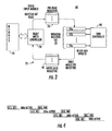
- a video multiviewer system 130 overcomes the drawbacks of transferring video streams to the graphics memory of a display that typically requires the use of an intermediate system memory buffer to manage the transfer between a hardware device and the display. It overcomes the disadvantages of consuming host CPU resources, memory resources, and bus bandwidth, thus overcoming a significant limit on the number of video streams than can be simultaneously displayed.
- DirectShow allows the transfer of video streams to video memory, but it requires CPU resources to manage the transfers.
- Typical prior art techniques use an input/output (I/O) controller to copy video stream data to system memory from the hardware device. The CPU copies the video stream data to the display device. This requires two separate DMA transfer operations. For relatively high bandwidth video streams, this may pose a significant limiting factor in a video system's capabilities, since DMA bandwidth has a fixed limit.
- the system 130 illustratively includes a video I/O controller 131, a system memory 132, and a Graphics Processing Unit (GPU) 133 including a GPU memory 134 in which video data is input using a video input module that includes the flexible DMA configuration and FPGA Block RAM as described before.
- the GPU memory 134 may include one or more texture buffers, which may be associated with respective video input streams or feeds, as will be appreciated by those skilled in the art.
- the system 130 also illustratively includes a central processing unit (CPU) 135. In the illustrated example, access between the video I/O controller 131, GPU 133, CPU 135, and system memory 132 is provided via a system bus 136, as will also be appreciated by those skilled in the art.
- the GPU is operable with a display 138.
- the video input module 140 receives data along the bus 136 and can be individual input modules that are used to DMA data into the GPU.
- PCI Express can be used as one non-limiting implementation.
- the video I/O controller 131 assigns addresses to be used for video data in the GPU memory 133 (i.e., texture buffers).
- texture buffers i.e., graphics processing units
- the texture buffers would temporarily be locked while textures are loaded from the video I/O controller to the texture buffers via the system memory 132. Drawing or rendering operations would not be permitted during such locked periods.
- the constant locking and unlocking of the texture buffers requires additional overhead, and therefore delays memory transfers.
- this can also result in a video I/O controller changing destination addresses in the GPU memory 134, which may result in a still further overhead penalty if the video I/O controller 131 has to be reset or reprogrammed to desired texture buffer addresses.
- the CPU 135 advantageously operates the video I/O controller 131 to transfer video data to the GPU memory 134 via direct memory access (DMA) without using the system memory 132. Accordingly, the system may advantageously increase the amount of video data transferred to the GPU 133 within a given amount of time, and thereby allow more video inputs to be displayed on the display than would otherwise be possible if the same video had to be routed through the system memory.
- DMA direct memory access
- the CPU may cooperate with the I/O controller 131 to lock the assigned addresses.
- the GPU memory 133 may include at least one texture buffer 134 in which the CPU locks the assigned addresses.
- the video I/O controller may receive a plurality of video input streams, and the at least one texture buffer may include a respective texture buffer for each video input stream.
- the CPU may operate the video I/O controller 131 and the GPU 133 to transfer video data in real time.
- the video multiviewer system may further include at least one data communications bus coupled to the video I/O controller 131, the system memory 132, the GPU 133 and the CPU 135.
- the video data may include video frame data.
- the CPU may use at least one Microsoft DirectX application programming interface (API) for operating the video I/O controller 131 and the GPU 133, for example.
- API Microsoft DirectX application programming interface
- the physical memory can address to allow the hardware I/O controller 131 to DMA transfer video stream data from the hardware device directly to the texture buffer. This technique does not require an intermediate host memory buffer for the video stream data thus saving this memory for other uses.
- This technique can rely on the fact that the GPU device driver does not change the physical memory address of the texture buffer and it remains available for the duration of the transfer.
- the system exploits an undocumented and unsupported behavior of the GPU device driver and the Microsoft DirectX run time. This allows a Centrio TM multiviewer as described above to make more efficient use of the hardware platform, thus providing more functionality with less hardware than competitive products. Since video frames are passed via DMA transfer once instead of twice, it effectively doubles the number of video streams the system could transfer otherwise.
- FIGS. 2-4 Further examples of a video multiviewer system that is adapted for enhanced scaling and can be modified for use with the flexible DMA configuration using the FPGA Block RAM described relative to FIGS. 2-4 is set forth below.
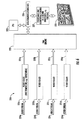
- a video multiviewer system 220 illustratively includes a plurality of video scalers 221a-221d operating in parallel for generating initially scaled video streams 225a-225d by performing video scaling in at least one dimension on a plurality of video input streams 224a-224d.
- Each video input stream 224a-242d may comprise a Society of Motion Picture and Television Engineers (SMPTE) 424M 3G-Serial Digital Interface (SDI) standard, for example.
- SMPTE Society of Motion Picture and Television Engineers
- SDI 3G-Serial Digital Interface
- the video multiviewer system 220 may alternatively receive less or more video input streams.
- the multiviewer system 220 illustratively includes a processing unit 227 coupled downstream from the video scalers 221a-221d for generating additionally scaled video streams (video output streams) by performing additional video scaling on the initially scaled video streams 225a-225d, and a display 230 cooperating with the processing unit for displaying multiple video windows based upon the additionally scaled video streams.
- the display 230 may comprise a plurality of screens, for example, 94 displays.
- the video multiviewer system 220 may scale the video input streams 224a-224d more efficiently by distributing the computationally intensive process of scaling the video input streams.
- each of the video scalers 221a-221d illustratively performs video scaling in only one dimension, for example, in a horizontal dimension of video frames.
- the processing unit 227 illustratively performs video scaling in a vertical dimension of video frames to complete the scaling of the video input streams 224a-224d.
- the computationally intensive vertical scaling which may use large amounts of storage and logic resources, may be performed by the processing unit 227.
- other distributions of the scaling processes may be implemented. In general, less intensive scaling processes should be allocated to the video scalers 221a-221d while the more complex scaling processes should be allocated to the processing unit 227.
- each of the video scalers 221a-221d may comprise a hardware implemented video scaler.
- the processing power of the video scalers 221a-221d may be limited and static.
- the video multiviewer system 220 allocates the horizontal scaling processes, which use fewer resources than the vertical scaling processes, to the video scalers 221a-221d.
- each of the video scalers 221a-221d may perform video scaling as a selectable power of 2, for example, 1, 2, 4, 8, and so forth, further reducing computational intensity demands on the video scalers.
- the size of the packaging and housing used for the video scalers is reduced.
- a single field-programmable gate array (FPGA) may be used to implement the video scalers 221a-221d to prescale 8 3G-SDI video input streams.
- the video scalers 221a-221d and the processing unit 227 illustratively cooperate to process data other than video stream data using distributed processing, for example, metadata extraction and audio ballistics metering. More specifically, the video scalers 221 a-221d may also perform bit data extraction, thereby advantageously reducing bandwidth passed on to the processing unit 227.
- the processing unit 227 may perform data decoding and interpretation based upon the bit data extraction.
- the video scalers 221a-221d may calculate raw ballistics values while the processing unit 227 cooperates to interpret the data and render appropriate audio amplitudes and phase meters.
- the processing unit 227 is preferably formed as a Graphics Processing Unit (GPU) including a GPU processor and GPU memory coupled thereto as noted relative to FIG. 5 . Moreso with the dedicated GPU memory, the processing unit 227 may efficiently handle the computationally and memory intensive vertical scaling tasks.
- GPU Graphics Processing Unit
- the video multiviewer system 220 illustratively includes a Direct Memory Access (DMA) engine 222 coupled between the video scalers 221a-221d and the processing unit (GPU) 227.
- DMA Direct Memory Access
- a second FPGA in addition to the FPGA that may implement the video scalers 221a-221d, may be used to implement the DMA engine 222.
- the video multiviewer system 220 illustratively includes a data communications bus 226 coupled between the DMA engine 222 and the processing unit (GPU) 227, and the CPU 223 coupled to the data communications bus.
- the DMA engine 222 "DMAs" the initially scaled video streams 225a-225d into the processing unit 227 for final scaling.
- the data communications bus 226 has an associated bandwidth and corresponding data throughput that may limit processing for scaling in the processing unit 227.
- the bandwidth bottleneck of the data communication bus 226 is less likely to be exceeded.
- the distributed scaling of the video multiviewer system 220 may allow for sufficiently offloading the processing unit 227 so that it handles the remaining scaling work, and the distributed scaling sufficiently reduces the DMA engine 222 bandwidth to "DMA" up to 64 video streams over modem local bus architectures, such as, PCI Express (1st generation) and Hyper Transport.
- the video multiviewer system 220 may be installed into a Platinum multiviewer, as available from the Harris Corporation of Melbourne, Florida (Harris Corp.), the assignee of the present application, or a router. Additionally, the video multiviewer system 220 may control routing of the video input streams 224a-224d. More specifically, the video multiviewer system 220 may access any of the router inputs, for example, that is all 512 inputs in a 28RU Platinum router, as available from the Harris Corp.
- the video multiviewer system 220 may additionally include multiple sets, all of which may be installed in the 28RU Platinum router, for example.
- the video multiviewer system 220 may selectively choose which set a video input stream routes to. Thereby, the video multiviewer system 220 may actively balance internal resource utilization between sets, and thus makes it possible to get better performance out of the same hardware.
- the video multiviewer system 220 can route it to two of its inputs, and apply different pre-scaling ratios to yield the best quality picture for both PIPS.
- PIPs picture-in-pictures
- the number of video input streams 224a-224d received by the video multiviewer system 220 is scalable.
- the number of inputs may be scalable based on the scalability of the 28RU Platinum Router.
- the number of outputs can be scaled up by inserting additional "sets" into the Platinum router frame, and each set may work independently of each other while having no limiting effect on other sets in the frame.
- a user may readily build a video multiviewer system 220 that spans a single video frame across two or more displays 230 driven by two or more sets, each set routing the same video stream to its input and displaying the corresponding portion of the video frame. This may allow for spanning a single video frame across a wall of displays.
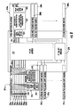
- the video multiviewer system 270 illustratively includes a plurality of Platinum Input Modules (PIMs) 271a-271n, as will be available from the Harris Corp. Each PIM 271a-271n illustratively receives eight video input streams.
- the video multiviewer system 270 may include up to 64 PIMs, receiving a total of 512 video input streams. The output of the PIMs 271a-271n is fed into a Platinum cross-point switcher 272, as will be available from the Harris Corp.
- the Platinum cross-point switcher 272 is fed into a plurality of Centrio modules 273a-273b, as will be available from the Harris Corp. Although illustrated with 2 Centrio modules 273a-273b, the video multiviewer system 270 may further include a total of 16 Centrio modules.
- Each Centrio module 273a-272b illustratively includes a plurality of video input modules 274a-274d feeding into a local data bus 275 cooperating with a CPU 279, and a GPU 276.
- the local data bus 275 may comprise, for example, a PCI Express (1st generation) data bus or a Hyper Transport data bus.
- the GPU 276 illustratively includes a data bus 277, a Random Access Memory module 281 cooperating with the data bus, and a scaler/rendering engine 280 cooperating with the data bus.
- the GPU 276 outputs to the input-output module 282 including a Digital Visual Interface (DVI) to SDI converter 283.
- DVI Digital Visual Interface
- the video multiviewer system 290 shown in FIG. 8 illustratively includes a plurality of Platinum Prescaling Input Modules (PPIMs) 291a-291n, as will be available from the Harris Corp. Each PPIM 291a-291n illustratively receives eight video input streams.
- PPIMs Platinum Prescaling Input Modules
- Each PPIM 291a-291n illustratively includes respective equalizers 296a-296h for each video input stream, and a prescaler module 294 including a deembedder 298 cooperating with a prescaler multiplexer 293.
- the deembedder 298 also includes an optional Dolby decoder 295.
- the outputs of the PPIMs 291a-291n are illustratively received by the Platinum cross-point matrix 297 and a Platinum TDM cross-point module 298, both as will be available from the Harris Corp.
- the outputs of the Platinum cross-point matrix 297 and the Platinum TDM cross-point module 298 are received by a plurality of multiviewer modules 300a-300n.
- Each multiviewer module 300a-300n illustratively includes a converter 301, a scaler module 302 receiving the output of the converter, and a DVI card (GPU) 303 receiving the output of the scaler module.
- the communication link between the PPIMs 291a-291n and the multiviewer modules 300a-300n may have a payload bandwidth divided into 8 equal parts, each allocated to one of the 8 video input streams (channels) on a given PPIM. After reserving space for a given channel's pre-processed ancillary space and audio ballistics information, the remaining bandwidth may be allocated for the video stream.
- the video pre-scaling ratio may be hardcoded on a per-video standard basis, and stored in a table for hardware automatic lookup. The pre-scaling ratio may be selected to result in the highest bandwidth that fits in the allocated payload bandwidth.
- the pre-processing parameters may be hardcoded at design or system integration phase and may not be dynamically changed.
- the packet size in the communications link may match the packet size used by multiviewer modules' 300a-300n local bus and DMA engine, thus minimizing logic required to handle the pre-processed data.
- the communications links in the video multiviewer system 290 follow the same profile. Any communication link may be used by the multiviewer modules 300a-300n without these modules interfering with each others operation.
- a single communication link may carry all 8 channels from a given input module, i.e., a multiviewer module 300a-300n may have full simultaneous access to up to 32 PPIMs 291a-291n , permitting greater access.
- This video multiviewer system 310 illustratively includes a plurality of first 28RU Platinum router frames 311a-311d, as will be available from the Harris Corp, each including a plurality of inputs 312, a cross-point switcher 313 coupled thereto, and a plurality of outputs 314 upstream of the cross-point switcher.
- the outputs 314 are received by a plurality of second 28RU Platinum router frames 316a-136d, each also including a plurality of inputs 317, a cross-point switcher 318 coupled thereto, and a plurality of outputs 319 upstream of the cross-point switcher.
- the video multiviewer system 310 illustratively receives 2048 SD/GD/3G-SDI video input streams and outputs 128 DVI outputs, or alternatively 256 HD-SDI outputs. As will be appreciated by those skilled in the art, the video multiviewer system 310 may be scaled to have more or less inputs and outputs.
Abstract
Description
- The present invention relates to the field of video processing systems, and more particularly, to video multiviewers and related methods.
- As broadcasters continue the transition from analog television to digital video television, the television production process is increasingly conducted in an all-digital domain, that is, from the initial camera shot to the display in the consumer's living room. This move to digital technology permits broadcasters to simultaneously broadcast multiple video streams using a single connection. Indeed, for popular live events, broadcasters typically deploy mobile broadcast units to route and manipulate, i.e., producing the numerous video streams that come from respective cameras throughout the event before being transmitted.
- An approach to manipulating and monitoring the video streams is a multiviewer, which typically includes a monitor and associated processor receiving the high resolution, digital video streams. The processor scales the video stream to fit all the video streams onto a single display. Some multiviewers use a plurality of monitors, thereby permitting the viewing of even more video streams. A potential drawback to the typical multiviewer is the difficulty in rearranging the video streams on the monitor in real time. For example, a user viewing the multiviewer monitor displaying four video streams split equally over quarters of the monitor may desire to expand a first video stream and correspondingly reduce the other video streams. This operation may cause the processor to adjust scaling operations in real time based upon requests from the user. More specifically, to provide advanced features to the user, the typical multiviewer may have to include significant hardware to provide adequate processing power, thereby possibly increasing the form factor and housing size to undesirable levels.
- An exemplary multiviewer system is the 7767VIP4 signal monitoring module from the Evertz corporation of Burlington, Ontario, Canada. The module simultaneously accepts, auto-detects, analyzes and displays four synchronous or asynchronous HD/SD/Analog video signals. An additional fifth computer graphic input may be used for display of a dynamic background image. A similar multiviewer system is disclosed in
U.S. Patent No. 7,023,488 to Szybiak et al. - Despite the advantages of such multiviewer systems, further enhancements may be desirable in some applications. For example, system memory constraints often impose restrictions on the number of video inputs that may be simultaneously displayed. Additionally, the ability of such systems to display added graphic content (e.g., backgrounds, indicators, etc.) along with the video inputs on the display may be encumbered by the requirement for separate inputs for such content, or for performing offline modifications to video inputs or display templates, for example.
-
US 2006/290708 discloses a graphics integrated circuit chip to be used in a set-top box for controlling a television display. The graphics chip processes analogue video input, digital video input, and graphics input. The chip includes a single polyphase filter that preferably provides anti-flutter filtering and scaling of graphics. The scaling of graphics is used to convert the normally square pixel aspect ratio of graphics to the normally rectangular pixel aspect ratio of video, The DMA machine is for accessing graphic window descriptors already present in memory. -
US2004/233230 discloses a DMA bus located between a North/South bridge and a GPU, and not between its I/O unit and its GPU memory. Video data is ultimately transferred to the GPU memory via a conventional bus between the GPU and the GPU memory. - The invention is as set out in
claims 1 and 6. - A video multiviewer system includes a Graphics Processing Unit (GPU) that includes a GPU memory. A video input module is operative with the GPU for receiving video data and transferring the video data to the GPU memory via a Direct Memory Access (DMA). A programmable circuit such as a Field Programmable Gate Array (FPGA) includes a multi-ported and in one aspect a dual ported block Random Access Memory (RAM) configured for a plurality of DMA channels for receiving video data and allowing uninterrupted operation of consecutive DMA transfers of video data to the GPU memory. A display displays the multiple video windows based upon video data received within the GPU memory.
- The system includes a DMA controller. The dual ported Block RAM includes first and second ports. The first port is operative for accessing video data based on independent read/write access and the second port is operative for accessing video data based on simultaneous read/write access by the DMA controller. The system also includes a read/write controller and plurality of registers. The DMA controller operates on DMA channel "n" and is operative for pre-reading registers for DMA channel "n+1." The DMA controller can change state variables in a register set when data is transferred within DMA channel "n." The DMA controller is also operative for modifying data within registers and passing the data back to the Read/write controller to be stored back within the Block RAM.
- This Block RAM is scaleable as to the number of DMA channels required for passing data to the GPU memory. A video data controller is operative with the video input module for assigning addresses to be used for video data within the GPU memory.
- Other objects, features and advantages of the present invention will become apparent from the detailed description of the invention which follows, when considered in light of the accompanying drawings in which:
-
FIG. 1 is a block diagram of a Field Programmable Gate Array (FPGA)/Application Specific Integrated Circuit (ASIC) implementation of configuration/state registers for a multi-channel Direct Memory Access. -
FIG. 2 is a block diagram showing Direct Memory Access (DMA) registers in Block Random Access Memory (RAM) of a Field Programmable Gate Array (FPGA) in accordance with a non-limiting example of the present invention. -
FIG. 3 is a block diagram showing the DMA registers in Block RAM for a register read/write logic function in accordance with a non-limiting example of the present invention. -
FIG. 4 is a timing pipeline for a single read/write Block RAM port to allow uninterrupted operation of consecutive DMA transfers in accordance with a non-limiting example of the present invention. -
FIG. 5 is a schematic block diagram of a video multiviewer system that provides a direct video data transfer to a GPU memory that could be modified to use the Block RAM DMA configuration in accordance with a non-limiting example of the present invention. -
FIG. 6 is a schematic block diagram of a video multiviewer system that can be modified to use the Block RAM DMA configuration in accordance with a non-limiting example of the present invention. -
FIG. 7 is a more detailed schematic block diagram of a video multiviewer system that can be modified to use the Block RAM DMA configuration in accordance with a non-limiting example of the present invention. -
FIG. 8 is a more detailed schematic block diagram of yet another video multiviewer system that can be modified to use the Block RAM DMA configuration in accordance with a non-limiting example of the present invention. -
FIG. 9 is yet another more detailed schematic block diagram of a video multiviewer system that can be modified to use the Block RAM DMA configuration in accordance with a non-limiting example of the present invention. - Different embodiments will now be described more fully hereinafter with reference to the accompanying drawings, in which preferred embodiments are shown. Many different forms can be set forth and described embodiments should not be construed as limited to the embodiments set forth herein. Rather, these embodiments are provided so that this disclosure will be thorough and complete, and will fully convey the scope to those skilled in the art. Like numbers refer to like elements throughout.
-
FIG. 1 is a block diagram of a DMA configured system 20 for Direct Memory Access (DMA) configuration/state registers using a multi-channel DMA. The block diagram shows aHost Write circuit 22 connected to a Write Decode circuit 24 and a number of Host/DMA Write Selectcircuits 26 that are arbitrated into a number of DMA channels formed in configuration/status registers inflip flops 30 and illustrated asDMA channel 1,DMA channel 2 and continuing to DMA channel "n." A secondWrite Decode circuit 32 is illustrated and receives Write Enable signals and Write Back Address signals from the DMA controller. TheseDMA channels 30 are formed as configuration/status registers in flip flops of a Field Programmable Gate Array circuit. The configuration/status registers inflip flops 30 output tovarious logic circuits 34 and output read data to aHost Read circuit 36 and theDMA controller 38 as illustrated. TheDMA controller 38 feeds back Write Back data, Write Back address and Write Enable signals to theWrite Decode circuit 32 and arbitrated writeselect circuit 26 along a respective WriteBack data line 40, WriteBack address line 42, and WriteEnable line 44 as illustrated. - In this implementation shown in
FIG. 1 , all configuration and state/status registers are stored in the FPGA flip flops, which is inefficient for storing large amounts of data. Additionally, any Write arbitration and decode logic and Read logic circuit are implemented in FPGA logic blocks. This results in an implementation that requires many flip flops and many resources, including FPGA logic resources. In addition, this circuit is not adequately scaleable and slows down with increased size. In this type of configuration, attempts to support many DMA channels result in a DMA configuration/state maintenance using many FPGA resources, which limits the speeds supported by the DMA. - In accordance with a non-limiting example of the present invention, most of this excess logic using FPGA flip flops is replaced using a multi-ported and in one aspect a dual ported Block RAM. As is known, RAM implementations typically permit access to a limited number of bits at a time, making Block RAM typically not applicable to general register files. In case of an application where only a subset of registers needs to be used at a time, such as with multi-channel DMA applications, it becomes possible to build a highly scalable solution using an FPGA Block RAM. It should be understood that different programmable circuits besides FPGA's can be used, including different types of ASIC's and other processors using Block RAM.
- A high-level diagram of a DMA configured
Block RAM system 50 as part of a video input module of a video multiviewer system having DMA registers in Block RAM is shown inFIG. 2 . The dual-ported nature of FPGA Block RAM allows independent read/write access by a Host such as a video controller or read/write controller for configuration through one port, and simultaneous read/write access by the DMA engine (controller or processor) via a second port. This eliminates a requirement for access arbitration logic. Any read/write decode and control logic is also already built into the Block RAM, thus eliminating a requirement for implementing it in FPGA logic as in DMA circuits such as shown inFIG. 1 . - An uninterrupted DMA video or other data for a video multiviewer is achieved through a large number of DMA channels while using Block RAM, which effectively has only a single read/write port.
FIG. 2 shows the high-level block diagram in which the Host Read and Writecircuit 52 is operable with a Read/Write Memory Interface 54 and each communicates with the other through appropriate Address (ADDR) lines, Data lines and Write Enable (WE) lines. The Read/Write Memory Interface 54 communicates with the Field Programmable Gate Array (FPGA) dual-portedBlock RAM 60 through a first port. TheBlock RAM 60 has a plurality of different DMA channels as illustrated, up to "n" and "n+1" DMA channels, which could be configured for as many as several thousand DMA channels. The dual-portedBlock RAM 60 is operable with another Read/Write Memory Interface 62 through the other port and thus to the DMA read/write circuit 64 and DMA controller (engine or processor), which collectively can be referred to as the DMA engine. The DMA Read/Write circuit 64 communicates using appropriate Address, Data and Write Enable signal lines with the Read/Write Memory Interface 62. -
FIG. 3 shows the DMA registers inBlock RAM 60 withMemory 70 and the register read/write logic circuit illustrated generally at 72. TheMemory 70 interfaces with the Read/Write controller 74 that is operable with the Pre-Read registers 76 and Working registers as aregister 78, formed as a plurality of workingregisters 78a, 78b ...78n that are operable with Reads and Updates to theDMA controller 66. ThisWorking Register Set 78 is operable with Write Back Registers 80 that are operable with the read/write controller 74 forming a loop circuit as illustrated. TheWorking Register Set 78 sends signals concerning only the modified registers with Reads and Updates for the video data to the DMA engine (or controller) 66. - The DMA register access logic is generally shown in this block diagram of
FIG. 3 . For efficient Read-Write Back data access a pipelined approach is utilized, such that theWorking Register Set 78 required for the next DMA channel "n" data transfer is Pre-Read ahead of time (note the Pre-Read Registers 76), and passed onto theDMA controller 60 when required. While the DMA controller operates on DMA channel "n," the read/write Controller 74 pre-reads registers for DMA channel "n+1." TheDMA controller 66 changes state variables in theWorking Register Set 78 as it performs the data transfer of channel "n." The data transfer is accomplished and the DMA controller (engine) 66 moves onto the next DMA channel (i.e., "n+1") and the modified data in registers are passed back to the Read/Write Controller 74 to be stored back into theBlock RAM 60. At this point, the system has its Write-Back logic "holding" registers 80 for DMA channel "n," theDMA controller 66 operating on DMA channel "n+1" registers, and the Pre-Read logic fetching registers for the next DAM channel "n+2." -
FIG. 4 shows timing of this pipeline, and demonstrates how a single read/write Block RAM port is sufficient to allow uninterrupted operation of consecutive DMA transfers. The logic required to implement this pipeline is significantly smaller than any arbitration/decode logic circuit required in a larger multi-channel DMA utilizing flip flops for configuration/state storage. - This FPGA Block RAM solution as described allows for scalability that is only limited by the size of available Block RAM memory in the FPGA. It can easily be scaled up to thousands of DMA channels without noticeable impact on speed and requires typically only additional storage space in Block RAM. A sample implementation can support 2,000 DMA channels, while utilizing a relatively small portion of the FPGA.
- The flexible DMA configuration using FPGA Block RAM as described is operable with the Graphic Processing Units (GPU) used in video multiviewer systems in which DMA signals are sent to texture memory or other Graphics Processing Units. These frames of video data are typically split into many blocks and sent as separate blocks over separate DMA channels into different memory locations for a video multiviewer system that has extensive scaling in one non-limiting embodiment. Different Field Programmable Gate Arrays could be used for this system, including FPGA's manufactured by Xylinx and Altera that use dual port Block RAMs. Thus, the system dual ports a Read/
Write Memory Interface 54 and interacts with theDMA controller 66 through a Read/Write Memory Interface 62 as shown inFIG. 2 . - Although a number of DMA channels could be implemented using registers and flip flops such as described relative to
FIG. 1 , the Block RAM approach as described in accordance with a non-limiting example of the present invention is advantageous. The additional logic that is required to select and control which register the system writes into is now part of the Block RAM, as well as the logic for reading, thus allowing greater amounts of Block RAM with many DMA channels. The Read/Write Decode function is built into the Block RAM. Because a hard DMA circuit is used, only a fraction of the registers need be accessed at a time, for example, in one non-limiting example, about a fifth of the registers. The system can have access to one of the registers out of an entire set of registers at one time. The system can go through fewer clock cycles to read the registers out for the next DMA transfer and the system can take the registers from the previous DMA transfer and write them back into the memory to store them. - From a design point of view, when using a minimum number of DMA channels, it is easier to implement a circuit for such minimum number of DMA channels in regular flip flops for speed and efficiency. When greater than 20 and 50 DMA channels are required, however, and expansion is necessary, the use of regular flip flops is not advantageous. When a large amount of video data for a multiviewer must be brought into the system, the greater number of DMA channels are required as described in accordance with a non-limiting example of the present invention. This system also allows greater ability to scale.
- For example, a DMA burst could be a block of 512 bytes for one DMA channel. The Read/
Write Controller 74 reads a corresponding configuration in the registers and processes data for thePre-Read Registers 76 and passes data onto theDMA controller 66, which operates on the registers such as on regular flip flops in function. Thus, the system increments the last written address and how much data has been sent across. When it returns, the system knows it has written the 512 bytes and is done sending those 512 bytes. It passes the resulting and updated information to any registers as status registers and back to the Write Back Registers 80. For example, if there is a list of a number of different DMA data bursts coming through during the first DMA, the Read/Write Controller 74 can pre-fetch the configuration information from the next DMA and theDMA controller 66 does not have to wait for the configuration for the second DMA burst to be read out since it is read out already and now ready to be used. Once theDMA controller 66 has processed the second DMA burst, the configuration in the status registers for the first DMA burst is in the Write Back registers 80 and written back into the memory by the Read/Write Controller 74. Thus, the system can achieve an uninterrupted DMA data flow through a large number of DMA channels while using effectively only a single read/write port as described. - It should be understood that it is possible to use the system as described further with different video multiviewer systems as described below.
- As shown in
FIG. 5 , avideo multiviewer system 130 overcomes the drawbacks of transferring video streams to the graphics memory of a display that typically requires the use of an intermediate system memory buffer to manage the transfer between a hardware device and the display. It overcomes the disadvantages of consuming host CPU resources, memory resources, and bus bandwidth, thus overcoming a significant limit on the number of video streams than can be simultaneously displayed. - One technology that is currently used for video rendering is Microsoft DirectShow, part of the DirectX family of API applications. DirectShow allows the transfer of video streams to video memory, but it requires CPU resources to manage the transfers. Typical prior art techniques use an input/output (I/O) controller to copy video stream data to system memory from the hardware device. The CPU copies the video stream data to the display device. This requires two separate DMA transfer operations. For relatively high bandwidth video streams, this may pose a significant limiting factor in a video system's capabilities, since DMA bandwidth has a fixed limit.
- As mentioned above, the
system 130 illustratively includes a video I/O controller 131, asystem memory 132, and a Graphics Processing Unit (GPU) 133 including aGPU memory 134 in which video data is input using a video input module that includes the flexible DMA configuration and FPGA Block RAM as described before. By way of example, theGPU memory 134 may include one or more texture buffers, which may be associated with respective video input streams or feeds, as will be appreciated by those skilled in the art. Thesystem 130 also illustratively includes a central processing unit (CPU) 135. In the illustrated example, access between the video I/O controller 131,GPU 133,CPU 135, andsystem memory 132 is provided via asystem bus 136, as will also be appreciated by those skilled in the art. The GPU is operable with adisplay 138. Thevideo input module 140 receives data along thebus 136 and can be individual input modules that are used to DMA data into the GPU. PCI Express can be used as one non-limiting implementation. - The video I/
O controller 131 assigns addresses to be used for video data in the GPU memory 133 (i.e., texture buffers). By way of comparison, using the DirectShow application discussed above, in a typical prior art arrangement the texture buffers would temporarily be locked while textures are loaded from the video I/O controller to the texture buffers via thesystem memory 132. Drawing or rendering operations would not be permitted during such locked periods. Yet, the constant locking and unlocking of the texture buffers requires additional overhead, and therefore delays memory transfers. Moreover, this can also result in a video I/O controller changing destination addresses in theGPU memory 134, which may result in a still further overhead penalty if the video I/O controller 131 has to be reset or reprogrammed to desired texture buffer addresses. - The
CPU 135 advantageously operates the video I/O controller 131 to transfer video data to theGPU memory 134 via direct memory access (DMA) without using thesystem memory 132. Accordingly, the system may advantageously increase the amount of video data transferred to theGPU 133 within a given amount of time, and thereby allow more video inputs to be displayed on the display than would otherwise be possible if the same video had to be routed through the system memory. - The CPU may cooperate with the I/
O controller 131 to lock the assigned addresses. By way of example, theGPU memory 133 may include at least onetexture buffer 134 in which the CPU locks the assigned addresses. Furthermore, the video I/O controller may receive a plurality of video input streams, and the at least one texture buffer may include a respective texture buffer for each video input stream. Moreover, the CPU may operate the video I/O controller 131 and theGPU 133 to transfer video data in real time. Also, the video multiviewer system may further include at least one data communications bus coupled to the video I/O controller 131, thesystem memory 132, theGPU 133 and theCPU 135. - By way of example, the video data may include video frame data. Furthermore, the CPU may use at least one Microsoft DirectX application programming interface (API) for operating the video I/
O controller 131 and theGPU 133, for example. By locking the texture buffer of the Direct3D texture, the physical memory can address to allow the hardware I/O controller 131 to DMA transfer video stream data from the hardware device directly to the texture buffer. This technique does not require an intermediate host memory buffer for the video stream data thus saving this memory for other uses. - This technique can rely on the fact that the GPU device driver does not change the physical memory address of the texture buffer and it remains available for the duration of the transfer. The system exploits an undocumented and unsupported behavior of the GPU device driver and the Microsoft DirectX run time. This allows a Centrio™ multiviewer as described above to make more efficient use of the hardware platform, thus providing more functionality with less hardware than competitive products. Since video frames are passed via DMA transfer once instead of twice, it effectively doubles the number of video streams the system could transfer otherwise.
- Further examples of a video multiviewer system that is adapted for enhanced scaling and can be modified for use with the flexible DMA configuration using the FPGA Block RAM described relative to
FIGS. 2-4 is set forth below. - Referring initially to
FIG. 6 , avideo multiviewer system 220 illustratively includes a plurality ofvideo scalers 221a-221d operating in parallel for generating initially scaledvideo streams 225a-225d by performing video scaling in at least one dimension on a plurality of video input streams 224a-224d. Each video input stream 224a-242d may comprise a Society of Motion Picture and Television Engineers (SMPTE) 424M 3G-Serial Digital Interface (SDI) standard, for example. Moreover, although illustrated as receiving 4 video input streams 224a-225d, thevideo multiviewer system 220 may alternatively receive less or more video input streams. - The
multiviewer system 220 illustratively includes aprocessing unit 227 coupled downstream from thevideo scalers 221a-221d for generating additionally scaled video streams (video output streams) by performing additional video scaling on the initially scaledvideo streams 225a-225d, and adisplay 230 cooperating with the processing unit for displaying multiple video windows based upon the additionally scaled video streams. Although illustrated as a single screen display, thedisplay 230 may comprise a plurality of screens, for example, 94 displays. Advantageously, thevideo multiviewer system 220 may scale the video input streams 224a-224d more efficiently by distributing the computationally intensive process of scaling the video input streams. - More particularly, each of the
video scalers 221a-221d illustratively performs video scaling in only one dimension, for example, in a horizontal dimension of video frames. Theprocessing unit 227 illustratively performs video scaling in a vertical dimension of video frames to complete the scaling of the video input streams 224a-224d. Advantageously, the computationally intensive vertical scaling, which may use large amounts of storage and logic resources, may be performed by theprocessing unit 227. As will be appreciated by those skilled in the art, other distributions of the scaling processes may be implemented. In general, less intensive scaling processes should be allocated to thevideo scalers 221a-221d while the more complex scaling processes should be allocated to theprocessing unit 227. - Additionally, each of the
video scalers 221a-221d may comprise a hardware implemented video scaler. In other words, the processing power of thevideo scalers 221a-221d may be limited and static. Advantageously, thevideo multiviewer system 220 allocates the horizontal scaling processes, which use fewer resources than the vertical scaling processes, to thevideo scalers 221a-221d. Moreover, each of thevideo scalers 221a-221d may perform video scaling as a selectable power of 2, for example, 1, 2, 4, 8, and so forth, further reducing computational intensity demands on the video scalers. Advantageously, since the computational demand on the hardware implementedvideo scalers 221a-221d is limited, the size of the packaging and housing used for the video scalers is reduced. For example, a single field-programmable gate array (FPGA) may be used to implement thevideo scalers 221a-221d toprescale 8 3G-SDI video input streams. - The
video scalers 221a-221d and theprocessing unit 227 illustratively cooperate to process data other than video stream data using distributed processing, for example, metadata extraction and audio ballistics metering. More specifically, the video scalers 221 a-221d may also perform bit data extraction, thereby advantageously reducing bandwidth passed on to theprocessing unit 227. Theprocessing unit 227 may perform data decoding and interpretation based upon the bit data extraction. Furthermore, to reduce the computational payload of a Central Processing Unit (CPU) 223 for audio processing, thevideo scalers 221a-221d may calculate raw ballistics values while theprocessing unit 227 cooperates to interpret the data and render appropriate audio amplitudes and phase meters. - The
processing unit 227 is preferably formed as a Graphics Processing Unit (GPU) including a GPU processor and GPU memory coupled thereto as noted relative toFIG. 5 . Moreso with the dedicated GPU memory, theprocessing unit 227 may efficiently handle the computationally and memory intensive vertical scaling tasks. - The
video multiviewer system 220 illustratively includes a Direct Memory Access (DMA)engine 222 coupled between thevideo scalers 221a-221d and the processing unit (GPU) 227. Also, a second FPGA, in addition to the FPGA that may implement thevideo scalers 221a-221d, may be used to implement theDMA engine 222. - The
video multiviewer system 220 illustratively includes adata communications bus 226 coupled between theDMA engine 222 and the processing unit (GPU) 227, and theCPU 223 coupled to the data communications bus. Advantageously, after the video input streams 224a-224d are prescaled, theDMA engine 222 "DMAs" the initially scaledvideo streams 225a-225d into theprocessing unit 227 for final scaling. - As will be appreciated by those skilled in the art, the
data communications bus 226 has an associated bandwidth and corresponding data throughput that may limit processing for scaling in theprocessing unit 227. Advantageously, in thevideo multiviewer system 220, since the scaling is distributed between thevideo scalers 221a-221d and theprocessing unit 227, the bandwidth bottleneck of thedata communication bus 226 is less likely to be exceeded. Indeed, the distributed scaling of thevideo multiviewer system 220 may allow for sufficiently offloading theprocessing unit 227 so that it handles the remaining scaling work, and the distributed scaling sufficiently reduces theDMA engine 222 bandwidth to "DMA" up to 64 video streams over modem local bus architectures, such as, PCI Express (1st generation) and Hyper Transport. - Advantageously, since the
video multiviewer system 220 consumes limited physical space, the system may be installed into a Platinum multiviewer, as available from the Harris Corporation of Melbourne, Florida (Harris Corp.), the assignee of the present application, or a router. Additionally, thevideo multiviewer system 220 may control routing of the video input streams 224a-224d. More specifically, thevideo multiviewer system 220 may access any of the router inputs, for example, that is all 512 inputs in a 28RU Platinum router, as available from the Harris Corp. - Although illustrated with a single plurality of
video scalers 221a-221d and acorresponding processing unit 227,data communications bus 226,CPU 223, and DMA engine 222 (all together hereinafter referenced as a "set"), in other embodiments, thevideo multiviewer system 220 may additionally include multiple sets, all of which may be installed in the 28RU Platinum router, for example. - The
video multiviewer system 220 may selectively choose which set a video input stream routes to. Thereby, thevideo multiviewer system 220 may actively balance internal resource utilization between sets, and thus makes it possible to get better performance out of the same hardware. - Moreover, if a user of the
video multiviewer system 220 chooses to display the same video input streams 224a-224d in two picture-in-pictures (PIPs) of different size, the video multiviewer system can route it to two of its inputs, and apply different pre-scaling ratios to yield the best quality picture for both PIPS. - Advantageously, the number of video input streams 224a-224d received by the
video multiviewer system 220 is scalable. In particular, the number of inputs may be scalable based on the scalability of the 28RU Platinum Router. Additionally, the number of outputs can be scaled up by inserting additional "sets" into the Platinum router frame, and each set may work independently of each other while having no limiting effect on other sets in the frame. - Since all sets in a frame have access to the same inputs, a user may readily build a
video multiviewer system 220 that spans a single video frame across two ormore displays 230 driven by two or more sets, each set routing the same video stream to its input and displaying the corresponding portion of the video frame. This may allow for spanning a single video frame across a wall of displays. - Referring to
FIG. 7 , as will be appreciated by those skilled in the art, an exemplary implementation of avideo multiviewer system 270, similar to themultiviewer 220 as shown inFIG. 1 , is now described. Thevideo multiviewer system 270 illustratively includes a plurality of Platinum Input Modules (PIMs) 271a-271n, as will be available from the Harris Corp. Each PIM 271a-271n illustratively receives eight video input streams. Thevideo multiviewer system 270 may include up to 64 PIMs, receiving a total of 512 video input streams. The output of thePIMs 271a-271n is fed into a Platinumcross-point switcher 272, as will be available from the Harris Corp. The Platinumcross-point switcher 272 is fed into a plurality of Centrio modules 273a-273b, as will be available from the Harris Corp. Although illustrated with 2 Centrio modules 273a-273b, thevideo multiviewer system 270 may further include a total of 16 Centrio modules. - Each Centrio module 273a-272b illustratively includes a plurality of video input modules 274a-274d feeding into a
local data bus 275 cooperating with aCPU 279, and aGPU 276. Thelocal data bus 275 may comprise, for example, a PCI Express (1st generation) data bus or a Hyper Transport data bus. TheGPU 276 illustratively includes adata bus 277, a RandomAccess Memory module 281 cooperating with the data bus, and a scaler/rendering engine 280 cooperating with the data bus. TheGPU 276 outputs to the input-output module 282 including a Digital Visual Interface (DVI) toSDI converter 283. - The video multiviewer system 290 shown in
FIG. 8 illustratively includes a plurality of Platinum Prescaling Input Modules (PPIMs) 291a-291n, as will be available from the Harris Corp. EachPPIM 291a-291n illustratively receives eight video input streams. - Each
PPIM 291a-291n illustratively includesrespective equalizers 296a-296h for each video input stream, and aprescaler module 294 including adeembedder 298 cooperating with aprescaler multiplexer 293. Thedeembedder 298 also includes anoptional Dolby decoder 295. The outputs of thePPIMs 291a-291n are illustratively received by the Platinumcross-point matrix 297 and a Platinum TDMcross-point module 298, both as will be available from the Harris Corp. The outputs of the Platinumcross-point matrix 297 and the Platinum TDMcross-point module 298 are received by a plurality ofmultiviewer modules 300a-300n. Eachmultiviewer module 300a-300n illustratively includes aconverter 301, ascaler module 302 receiving the output of the converter, and a DVI card (GPU) 303 receiving the output of the scaler module. - The communication link between the
PPIMs 291a-291n and themultiviewer modules 300a-300n may have a payload bandwidth divided into 8 equal parts, each allocated to one of the 8 video input streams (channels) on a given PPIM. After reserving space for a given channel's pre-processed ancillary space and audio ballistics information, the remaining bandwidth may be allocated for the video stream. The video pre-scaling ratio may be hardcoded on a per-video standard basis, and stored in a table for hardware automatic lookup. The pre-scaling ratio may be selected to result in the highest bandwidth that fits in the allocated payload bandwidth. - The pre-processing parameters may be hardcoded at design or system integration phase and may not be dynamically changed. The packet size in the communications link may match the packet size used by multiviewer modules' 300a-300n local bus and DMA engine, thus minimizing logic required to handle the pre-processed data.
- Advantageously, the communications links in the video multiviewer system 290 follow the same profile. Any communication link may be used by the
multiviewer modules 300a-300n without these modules interfering with each others operation. A single communication link may carry all 8 channels from a given input module, i.e., amultiviewer module 300a-300n may have full simultaneous access to up to 32PPIMs 291a-291n, permitting greater access. - Referring now to
FIG. 9 , as will be appreciated by those skilled in the art, another exemplary implementation of the video multiviewer system 220 (FIG. 1 ), is now described. This video multiviewer system 310 illustratively includes a plurality of first 28RUPlatinum router frames 311a-311d, as will be available from the Harris Corp, each including a plurality ofinputs 312, across-point switcher 313 coupled thereto, and a plurality ofoutputs 314 upstream of the cross-point switcher. - The
outputs 314 are received by a plurality of second 28RU Platinum router frames 316a-136d, each also including a plurality ofinputs 317, across-point switcher 318 coupled thereto, and a plurality of outputs 319 upstream of the cross-point switcher. The video multiviewer system 310 illustratively receives 2048 SD/GD/3G-SDI video input streams and outputs 128 DVI outputs, or alternatively 256 HD-SDI outputs. As will be appreciated by those skilled in the art, the video multiviewer system 310 may be scaled to have more or less inputs and outputs.
Claims (10)
- A video multiviewer system (220) comprising:a graphics processing unit (GPU) (133, 227) comprising a GPU memory (134);a video input module (140) operable with the GPU for receiving incoming video data and transferring the incoming video data to the GPU memory via Direct Memory Access (DMA) (222), and further comprising a programmable circuit having multi-ported Block Random Access Memory (RAM) (60) configured for a plurality of DMA channels for receiving the incoming video data and allowing uninterrupted operation of consecutive DMA transfers of the incoming video data to the GPU memory (134); anda display (138, 230) for displaying multiple video windows based upon the incoming video data received within said GPU memory (134).
- The video multiviewer system according to Claim 1, and further comprising a DMA controller (66), wherein said multi-ported Block RAM (60) comprises first and second ports, wherein said first port is operative for accessing the incoming video data (52) based on independent read/write access (54) and the second port is operative for accessing the incoming video data based on simultaneous read/write (62) access by said DMA controller (66).
- The video multiviewer system according to Claim 2, and further comprising a Read/Write controller (74) and a plurality of registers (76, 78, 80), wherein as said DMA controller (66) operates on DMA channel "n," the Read/Write controller (74) is operative for pre-reading registers for DMA channel "n + 1."
- The video multiviewer system according to Claim 3, wherein said DMA controller (66) changes state variables in registers when data is transferred within DMA Y channel "n."
- The video multiviewer system according to Claim 3, wherein said DMA controller (66) is operative for modifying data within registers and passing data back to the Read/Write controller (74) to be stored back within the Block RAM (60).
- A method for displaying multiple video windows on a video multiviewer display (138, 230) comprising:a video input module (140) operable with a GPU (133) for receiving incoming video data within a video input module connected to a Graphics Processing Unit (GPU) having a GPU memory (134);transferring the incoming video data to the GPU memory (134) via Direct Memory Access (DMA) (66) through a programmable circuit having a multi-ported Block Random Access Memory (RAM) (60) configured for a plurality of DMA channels for receiving the incoming video data and allowing uninterrupted operation of consecutive DMA transfers of the incoming video data to the GPU memory (134); anddisplaying (138, 230) multiple video windows on a multiviewer display based upon the incoming video data received in the GPU mernory (134).
- The method according to Claim 6, which further comprises independently accessing (54) the incoming video data (52) in association with a Read/Write controller (74) while simultaneously accessing the incoming video data with a DMA controller (66).
- The method according to Claim 7, which further comprises operating on DMA channel "n" with the DMA controller while the Read/Write controller (74) pre- reads registers (76, 78, 80) for DMA channel "n + 1."
- The method according to Claim 7, which further comprises changing state variables in registers (76, 78, 80) while transferring data within DMA channel "n."
- The method according to Claim 7, which further comprises modifying data within registers and passing data back to the Read/Write controller (74) to be stored back within Block RAM (60).
Applications Claiming Priority (2)
| Application Number | Priority Date | Filing Date | Title |
|---|---|---|---|
| US12/099,380 US9438844B2 (en) | 2008-04-08 | 2008-04-08 | Video multiviewer system using direct memory access (DMA) registers and block RAM |
| PCT/US2009/039856 WO2009126679A1 (en) | 2008-04-08 | 2009-04-08 | Video multiviewer system using direct memory access (dma) registers and multi ported block ram and related method |
Publications (2)
| Publication Number | Publication Date |
|---|---|
| EP2274908A1 EP2274908A1 (en) | 2011-01-19 |
| EP2274908B1 true EP2274908B1 (en) | 2011-11-02 |
Family
ID=40775163
Family Applications (1)
| Application Number | Title | Priority Date | Filing Date |
|---|---|---|---|
| EP09730475A Active EP2274908B1 (en) | 2008-04-08 | 2009-04-08 | Video multiviewer system using direct memory access (dma) registers and multi ported block ram and related method |
Country Status (5)
| Country | Link |
|---|---|
| US (1) | US9438844B2 (en) |
| EP (1) | EP2274908B1 (en) |
| AT (1) | ATE532329T1 (en) |
| CA (1) | CA2661678C (en) |
| WO (1) | WO2009126679A1 (en) |
Families Citing this family (11)
| Publication number | Priority date | Publication date | Assignee | Title |
|---|---|---|---|---|
| US9716854B2 (en) * | 2008-04-09 | 2017-07-25 | Imagine Communications Corp. | Video multiviewer system with distributed scaling and related methods |
| CN101859334B (en) * | 2010-05-17 | 2012-06-13 | 山东大学 | Design method of interconnection cache structure of video decoding module and video display processing module |
| US9076259B2 (en) | 2011-09-14 | 2015-07-07 | Imagine Communications Corp | Geospatial multiviewer |
| US9304730B2 (en) * | 2012-08-23 | 2016-04-05 | Microsoft Technology Licensing, Llc | Direct communication between GPU and FPGA components |
| CN102905056B (en) * | 2012-10-18 | 2015-09-02 | 利亚德光电股份有限公司 | Method of video image processing and device |
| US20140267395A1 (en) * | 2013-03-13 | 2014-09-18 | Ross Video Limited | Low-latency interactive multiviewer interfaces and methods for video broadcast equipment |
| CN105430303B (en) * | 2015-11-10 | 2019-05-17 | 恒宇信通航空装备(北京)股份有限公司 | Graphics accelerator based on FPGA in a kind of military airborne cockpit display system |
| WO2018039482A1 (en) * | 2016-08-24 | 2018-03-01 | Raduchel William J | Network-enabled graphics processing module |
| CN106776373B (en) * | 2017-01-12 | 2020-10-16 | 合肥速显微电子科技有限公司 | Flash-memory-based cache system and method for mobile equipment |
| US10332235B1 (en) | 2018-05-01 | 2019-06-25 | At&T Intellectual Property I, L.P. | Direct memory access for graphics processing unit packet processing |
| US10795840B2 (en) | 2018-11-12 | 2020-10-06 | At&T Intellectual Property I, L.P. | Persistent kernel for graphics processing unit direct memory access network packet processing |
Family Cites Families (14)
| Publication number | Priority date | Publication date | Assignee | Title |
|---|---|---|---|---|
| US5099331A (en) * | 1987-09-04 | 1992-03-24 | Texas Instruments Incorporated | Apparatus for overlaying a displayed image with a second image |
| US5386532A (en) * | 1991-12-30 | 1995-01-31 | Sun Microsystems, Inc. | Method and apparatus for transferring data between a memory and a plurality of peripheral units through a plurality of data channels |
| US5420984A (en) * | 1992-06-30 | 1995-05-30 | Genroco, Inc. | Apparatus and method for rapid switching between control of first and second DMA circuitry to effect rapid switching beween DMA communications |
| US5848264A (en) * | 1996-10-25 | 1998-12-08 | S3 Incorporated | Debug and video queue for multi-processor chip |
| US5978866A (en) * | 1997-03-10 | 1999-11-02 | Integrated Technology Express, Inc. | Distributed pre-fetch buffer for multiple DMA channel device |
| US5933855A (en) * | 1997-03-21 | 1999-08-03 | Rubinstein; Richard | Shared, reconfigurable memory architectures for digital signal processing |
| US6895452B1 (en) * | 1997-06-04 | 2005-05-17 | Marger Johnson & Mccollom, P.C. | Tightly coupled and scalable memory and execution unit architecture |
| US6570579B1 (en) * | 1998-11-09 | 2003-05-27 | Broadcom Corporation | Graphics display system |
| JP2002112992A (en) * | 2000-06-30 | 2002-04-16 | Canon Inc | Apparatus and method for processing signal, and imaging device |
| CA2379782C (en) * | 2001-04-20 | 2010-11-02 | Evertz Microsystems Ltd. | Circuit and method for live switching of digital video programs containing embedded audio data |
| US6963348B2 (en) * | 2002-05-31 | 2005-11-08 | Nvidia Corporation | Method and apparatus for display image adjustment |
| US7456851B2 (en) * | 2003-05-20 | 2008-11-25 | Honeywell International Inc. | Method and apparatus for spatial compensation for pixel pattern on LCD displays |
| US20070268317A1 (en) * | 2006-05-18 | 2007-11-22 | Dan Banay | User interface system and method for selectively displaying a portion of a display screen |
| US7536669B1 (en) * | 2006-08-30 | 2009-05-19 | Xilinx, Inc. | Generic DMA IP core interface for FPGA platform design |
-
2008
- 2008-04-08 US US12/099,380 patent/US9438844B2/en active Active
-
2009
- 2009-04-07 CA CA2661678A patent/CA2661678C/en active Active
- 2009-04-08 EP EP09730475A patent/EP2274908B1/en active Active
- 2009-04-08 WO PCT/US2009/039856 patent/WO2009126679A1/en active Application Filing
- 2009-04-08 AT AT09730475T patent/ATE532329T1/en active
Also Published As
| Publication number | Publication date |
|---|---|
| US9438844B2 (en) | 2016-09-06 |
| US20090254683A1 (en) | 2009-10-08 |
| ATE532329T1 (en) | 2011-11-15 |
| CA2661678C (en) | 2014-09-09 |
| CA2661678A1 (en) | 2009-10-08 |
| EP2274908A1 (en) | 2011-01-19 |
| WO2009126679A1 (en) | 2009-10-15 |
Similar Documents
| Publication | Publication Date | Title |
|---|---|---|
| EP2274908B1 (en) | Video multiviewer system using direct memory access (dma) registers and multi ported block ram and related method | |
| US6353460B1 (en) | Television receiver, video signal processing device, image processing device and image processing method | |
| CA2661771C (en) | Video multiviewer system with serial digital interface and related methods | |
| US8738891B1 (en) | Methods and systems for command acceleration in a video processor via translation of scalar instructions into vector instructions | |
| KR102520330B1 (en) | Display controller | |
| US5909225A (en) | Frame buffer cache for graphics applications | |
| US8811499B2 (en) | Video multiviewer system permitting scrolling of multiple video windows and related methods | |
| CA2661760C (en) | Video multiviewer system with switcher and distributed scaling and related methods | |
| US7307667B1 (en) | Method and apparatus for an integrated high definition television controller | |
| CA2661768C (en) | Video multiviewer system with distributed scaling and related methods | |
| US7479965B1 (en) | Optimized alpha blend for anti-aliased render | |
| EP1987488A2 (en) | Combined engine for video and graphics processing | |
| US10216412B2 (en) | Data processing systems | |
| CA2661756C (en) | Video multiviewer system providing direct video data transfer to graphics processing unit (gpu) memory and related methods | |
| CN101257588B (en) | Image processing system and method for processing television divided pictures | |
| JP2005086822A (en) | Apparatus to process video data and graphic data | |
| KR20210150704A (en) | Line interleaving controller and image signal processor including the same |
Legal Events
| Date | Code | Title | Description |
|---|---|---|---|
| PUAI | Public reference made under article 153(3) epc to a published international application that has entered the european phase |
Free format text: ORIGINAL CODE: 0009012 |
|
| 17P | Request for examination filed |
Effective date: 20101026 |
|
| AK | Designated contracting states |
Kind code of ref document: A1 Designated state(s): AT BE BG CH CY CZ DE DK EE ES FI FR GB GR HR HU IE IS IT LI LT LU LV MC MK MT NL NO PL PT RO SE SI SK TR |
|
| AX | Request for extension of the european patent |
Extension state: AL BA RS |
|
| GRAP | Despatch of communication of intention to grant a patent |
Free format text: ORIGINAL CODE: EPIDOSNIGR1 |
|
| DAX | Request for extension of the european patent (deleted) | ||
| GRAS | Grant fee paid |
Free format text: ORIGINAL CODE: EPIDOSNIGR3 |
|
| GRAA | (expected) grant |
Free format text: ORIGINAL CODE: 0009210 |
|
| AK | Designated contracting states |
Kind code of ref document: B1 Designated state(s): AT BE BG CH CY CZ DE DK EE ES FI FR GB GR HR HU IE IS IT LI LT LU LV MC MK MT NL NO PL PT RO SE SI SK TR |
|
| REG | Reference to a national code |
Ref country code: GB Ref legal event code: FG4D |
|
| REG | Reference to a national code |
Ref country code: CH Ref legal event code: EP |
|
| REG | Reference to a national code |
Ref country code: IE Ref legal event code: FG4D |
|
| REG | Reference to a national code |
Ref country code: DE Ref legal event code: R096 Ref document number: 602009003467 Country of ref document: DE Effective date: 20120202 |
|
| REG | Reference to a national code |
Ref country code: NL Ref legal event code: VDEP Effective date: 20111102 |
|
| LTIE | Lt: invalidation of european patent or patent extension |
Effective date: 20111102 |
|
| PG25 | Lapsed in a contracting state [announced via postgrant information from national office to epo] |
Ref country code: LT Free format text: LAPSE BECAUSE OF FAILURE TO SUBMIT A TRANSLATION OF THE DESCRIPTION OR TO PAY THE FEE WITHIN THE PRESCRIBED TIME-LIMIT Effective date: 20111102 Ref country code: IS Free format text: LAPSE BECAUSE OF FAILURE TO SUBMIT A TRANSLATION OF THE DESCRIPTION OR TO PAY THE FEE WITHIN THE PRESCRIBED TIME-LIMIT Effective date: 20120302 Ref country code: NO Free format text: LAPSE BECAUSE OF FAILURE TO SUBMIT A TRANSLATION OF THE DESCRIPTION OR TO PAY THE FEE WITHIN THE PRESCRIBED TIME-LIMIT Effective date: 20120202 |
|
| PG25 | Lapsed in a contracting state [announced via postgrant information from national office to epo] |
Ref country code: NL Free format text: LAPSE BECAUSE OF FAILURE TO SUBMIT A TRANSLATION OF THE DESCRIPTION OR TO PAY THE FEE WITHIN THE PRESCRIBED TIME-LIMIT Effective date: 20111102 Ref country code: HR Free format text: LAPSE BECAUSE OF FAILURE TO SUBMIT A TRANSLATION OF THE DESCRIPTION OR TO PAY THE FEE WITHIN THE PRESCRIBED TIME-LIMIT Effective date: 20111102 Ref country code: SE Free format text: LAPSE BECAUSE OF FAILURE TO SUBMIT A TRANSLATION OF THE DESCRIPTION OR TO PAY THE FEE WITHIN THE PRESCRIBED TIME-LIMIT Effective date: 20111102 Ref country code: LV Free format text: LAPSE BECAUSE OF FAILURE TO SUBMIT A TRANSLATION OF THE DESCRIPTION OR TO PAY THE FEE WITHIN THE PRESCRIBED TIME-LIMIT Effective date: 20111102 Ref country code: GR Free format text: LAPSE BECAUSE OF FAILURE TO SUBMIT A TRANSLATION OF THE DESCRIPTION OR TO PAY THE FEE WITHIN THE PRESCRIBED TIME-LIMIT Effective date: 20120203 Ref country code: SI Free format text: LAPSE BECAUSE OF FAILURE TO SUBMIT A TRANSLATION OF THE DESCRIPTION OR TO PAY THE FEE WITHIN THE PRESCRIBED TIME-LIMIT Effective date: 20111102 Ref country code: PL Free format text: LAPSE BECAUSE OF FAILURE TO SUBMIT A TRANSLATION OF THE DESCRIPTION OR TO PAY THE FEE WITHIN THE PRESCRIBED TIME-LIMIT Effective date: 20111102 Ref country code: PT Free format text: LAPSE BECAUSE OF FAILURE TO SUBMIT A TRANSLATION OF THE DESCRIPTION OR TO PAY THE FEE WITHIN THE PRESCRIBED TIME-LIMIT Effective date: 20120302 |
|
| PG25 | Lapsed in a contracting state [announced via postgrant information from national office to epo] |
Ref country code: CY Free format text: LAPSE BECAUSE OF FAILURE TO SUBMIT A TRANSLATION OF THE DESCRIPTION OR TO PAY THE FEE WITHIN THE PRESCRIBED TIME-LIMIT Effective date: 20111102 |
|
| PG25 | Lapsed in a contracting state [announced via postgrant information from national office to epo] |
Ref country code: EE Free format text: LAPSE BECAUSE OF FAILURE TO SUBMIT A TRANSLATION OF THE DESCRIPTION OR TO PAY THE FEE WITHIN THE PRESCRIBED TIME-LIMIT Effective date: 20111102 Ref country code: CZ Free format text: LAPSE BECAUSE OF FAILURE TO SUBMIT A TRANSLATION OF THE DESCRIPTION OR TO PAY THE FEE WITHIN THE PRESCRIBED TIME-LIMIT Effective date: 20111102 Ref country code: BG Free format text: LAPSE BECAUSE OF FAILURE TO SUBMIT A TRANSLATION OF THE DESCRIPTION OR TO PAY THE FEE WITHIN THE PRESCRIBED TIME-LIMIT Effective date: 20120202 Ref country code: SK Free format text: LAPSE BECAUSE OF FAILURE TO SUBMIT A TRANSLATION OF THE DESCRIPTION OR TO PAY THE FEE WITHIN THE PRESCRIBED TIME-LIMIT Effective date: 20111102 Ref country code: DK Free format text: LAPSE BECAUSE OF FAILURE TO SUBMIT A TRANSLATION OF THE DESCRIPTION OR TO PAY THE FEE WITHIN THE PRESCRIBED TIME-LIMIT Effective date: 20111102 |
|
| PG25 | Lapsed in a contracting state [announced via postgrant information from national office to epo] |
Ref country code: RO Free format text: LAPSE BECAUSE OF FAILURE TO SUBMIT A TRANSLATION OF THE DESCRIPTION OR TO PAY THE FEE WITHIN THE PRESCRIBED TIME-LIMIT Effective date: 20111102 Ref country code: IT Free format text: LAPSE BECAUSE OF FAILURE TO SUBMIT A TRANSLATION OF THE DESCRIPTION OR TO PAY THE FEE WITHIN THE PRESCRIBED TIME-LIMIT Effective date: 20111102 |
|
| PLBE | No opposition filed within time limit |
Free format text: ORIGINAL CODE: 0009261 |
|
| STAA | Information on the status of an ep patent application or granted ep patent |
Free format text: STATUS: NO OPPOSITION FILED WITHIN TIME LIMIT |
|
| REG | Reference to a national code |
Ref country code: AT Ref legal event code: MK05 Ref document number: 532329 Country of ref document: AT Kind code of ref document: T Effective date: 20111102 |
|
| 26N | No opposition filed |
Effective date: 20120803 |
|
| REG | Reference to a national code |
Ref country code: DE Ref legal event code: R097 Ref document number: 602009003467 Country of ref document: DE Effective date: 20120803 |
|
| PG25 | Lapsed in a contracting state [announced via postgrant information from national office to epo] |
Ref country code: MC Free format text: LAPSE BECAUSE OF NON-PAYMENT OF DUE FEES Effective date: 20120430 |
|
| PG25 | Lapsed in a contracting state [announced via postgrant information from national office to epo] |
Ref country code: AT Free format text: LAPSE BECAUSE OF FAILURE TO SUBMIT A TRANSLATION OF THE DESCRIPTION OR TO PAY THE FEE WITHIN THE PRESCRIBED TIME-LIMIT Effective date: 20111102 |
|
| REG | Reference to a national code |
Ref country code: DE Ref legal event code: R119 Ref document number: 602009003467 Country of ref document: DE Effective date: 20121101 |
|
| PG25 | Lapsed in a contracting state [announced via postgrant information from national office to epo] |
Ref country code: MK Free format text: LAPSE BECAUSE OF FAILURE TO SUBMIT A TRANSLATION OF THE DESCRIPTION OR TO PAY THE FEE WITHIN THE PRESCRIBED TIME-LIMIT Effective date: 20111102 |
|
| PG25 | Lapsed in a contracting state [announced via postgrant information from national office to epo] |
Ref country code: ES Free format text: LAPSE BECAUSE OF FAILURE TO SUBMIT A TRANSLATION OF THE DESCRIPTION OR TO PAY THE FEE WITHIN THE PRESCRIBED TIME-LIMIT Effective date: 20120213 |
|
| PG25 | Lapsed in a contracting state [announced via postgrant information from national office to epo] |
Ref country code: FI Free format text: LAPSE BECAUSE OF FAILURE TO SUBMIT A TRANSLATION OF THE DESCRIPTION OR TO PAY THE FEE WITHIN THE PRESCRIBED TIME-LIMIT Effective date: 20111102 |
|
| PG25 | Lapsed in a contracting state [announced via postgrant information from national office to epo] |
Ref country code: MT Free format text: LAPSE BECAUSE OF FAILURE TO SUBMIT A TRANSLATION OF THE DESCRIPTION OR TO PAY THE FEE WITHIN THE PRESCRIBED TIME-LIMIT Effective date: 20111102 |
|
| REG | Reference to a national code |
Ref country code: FR Ref legal event code: TP Owner name: HBC SOLUTIONS, INC., US Effective date: 20130807 |
|
| REG | Reference to a national code |
Ref country code: GB Ref legal event code: 732E Free format text: REGISTERED BETWEEN 20130815 AND 20130821 |
|
| REG | Reference to a national code |
Ref country code: CH Ref legal event code: PL |
|
| PG25 | Lapsed in a contracting state [announced via postgrant information from national office to epo] |
Ref country code: LI Free format text: LAPSE BECAUSE OF NON-PAYMENT OF DUE FEES Effective date: 20130430 Ref country code: CH Free format text: LAPSE BECAUSE OF NON-PAYMENT OF DUE FEES Effective date: 20130430 |
|
| BECA | Be: change of holder's address |
Owner name: HBC SOLUTIONS, INC. Effective date: 20140401 Owner name: 9800 SOUTH MERIDIAN BOULEVARD SUITE 300,ENGLEWOOD Effective date: 20140401 |
|
| PG25 | Lapsed in a contracting state [announced via postgrant information from national office to epo] |
Ref country code: TR Free format text: LAPSE BECAUSE OF FAILURE TO SUBMIT A TRANSLATION OF THE DESCRIPTION OR TO PAY THE FEE WITHIN THE PRESCRIBED TIME-LIMIT Effective date: 20111102 |
|
| PG25 | Lapsed in a contracting state [announced via postgrant information from national office to epo] |
Ref country code: LU Free format text: LAPSE BECAUSE OF NON-PAYMENT OF DUE FEES Effective date: 20120408 |
|
| REG | Reference to a national code |
Ref country code: FR Ref legal event code: CA Effective date: 20140514 |
|
| PG25 | Lapsed in a contracting state [announced via postgrant information from national office to epo] |
Ref country code: HU Free format text: LAPSE BECAUSE OF FAILURE TO SUBMIT A TRANSLATION OF THE DESCRIPTION OR TO PAY THE FEE WITHIN THE PRESCRIBED TIME-LIMIT Effective date: 20090408 |
|
| PG25 | Lapsed in a contracting state [announced via postgrant information from national office to epo] |
Ref country code: DE Free format text: LAPSE BECAUSE OF FAILURE TO SUBMIT A TRANSLATION OF THE DESCRIPTION OR TO PAY THE FEE WITHIN THE PRESCRIBED TIME-LIMIT Effective date: 20121101 |
|
| REG | Reference to a national code |
Ref country code: FR Ref legal event code: PLFP Year of fee payment: 8 |
|
| REG | Reference to a national code |
Ref country code: FR Ref legal event code: PLFP Year of fee payment: 9 |
|
| REG | Reference to a national code |
Ref country code: BE Ref legal event code: HC Owner name: IMAGINE COMMUNICATIONS CORP.; US Free format text: DETAILS ASSIGNMENT: CHANGE OF OWNER(S), CHANGEMENT NOM PROPRIETAIRE, NOM/ADRESSE; FORMER OWNER NAME: HBC SOLUTIONS, INC. Effective date: 20170831 |
|
| REG | Reference to a national code |
Ref country code: FR Ref legal event code: CA Effective date: 20171227 Ref country code: FR Ref legal event code: CD Owner name: IMAGINE COMMUNICATIONS CORP., US Effective date: 20171227 |
|
| REG | Reference to a national code |
Ref country code: FR Ref legal event code: PLFP Year of fee payment: 10 |
|
| PGFP | Annual fee paid to national office [announced via postgrant information from national office to epo] |
Ref country code: IE Payment date: 20230427 Year of fee payment: 15 Ref country code: FR Payment date: 20230425 Year of fee payment: 15 |
|
| PGFP | Annual fee paid to national office [announced via postgrant information from national office to epo] |
Ref country code: BE Payment date: 20230427 Year of fee payment: 15 |
|
| PGFP | Annual fee paid to national office [announced via postgrant information from national office to epo] |
Ref country code: GB Payment date: 20230427 Year of fee payment: 15 |