EP0985902A1 - Interferometrische Vorrichtung zum Sichtbarmachung von Optischen Reflexion- und/oder Transmissionscharakteristiken im inneren eines Objektes - Google Patents
Interferometrische Vorrichtung zum Sichtbarmachung von Optischen Reflexion- und/oder Transmissionscharakteristiken im inneren eines Objektes Download PDFInfo
- Publication number
- EP0985902A1 EP0985902A1 EP99402227A EP99402227A EP0985902A1 EP 0985902 A1 EP0985902 A1 EP 0985902A1 EP 99402227 A EP99402227 A EP 99402227A EP 99402227 A EP99402227 A EP 99402227A EP 0985902 A1 EP0985902 A1 EP 0985902A1
- Authority
- EP
- European Patent Office
- Prior art keywords
- interferometric device
- photosensor
- source
- lenses
- xmzn
- Prior art date
- Legal status (The legal status is an assumption and is not a legal conclusion. Google has not performed a legal analysis and makes no representation as to the accuracy of the status listed.)
- Granted
Links
Images


Classifications
-
- G—PHYSICS
- G01—MEASURING; TESTING
- G01B—MEASURING LENGTH, THICKNESS OR SIMILAR LINEAR DIMENSIONS; MEASURING ANGLES; MEASURING AREAS; MEASURING IRREGULARITIES OF SURFACES OR CONTOURS
- G01B9/00—Measuring instruments characterised by the use of optical techniques
- G01B9/02—Interferometers
- G01B9/02015—Interferometers characterised by the beam path configuration
- G01B9/02027—Two or more interferometric channels or interferometers
- G01B9/02028—Two or more reference or object arms in one interferometer
-
- G—PHYSICS
- G01—MEASURING; TESTING
- G01B—MEASURING LENGTH, THICKNESS OR SIMILAR LINEAR DIMENSIONS; MEASURING ANGLES; MEASURING AREAS; MEASURING IRREGULARITIES OF SURFACES OR CONTOURS
- G01B11/00—Measuring arrangements characterised by the use of optical techniques
- G01B11/02—Measuring arrangements characterised by the use of optical techniques for measuring length, width or thickness
- G01B11/026—Measuring arrangements characterised by the use of optical techniques for measuring length, width or thickness by measuring distance between sensor and object
-
- G—PHYSICS
- G01—MEASURING; TESTING
- G01B—MEASURING LENGTH, THICKNESS OR SIMILAR LINEAR DIMENSIONS; MEASURING ANGLES; MEASURING AREAS; MEASURING IRREGULARITIES OF SURFACES OR CONTOURS
- G01B11/00—Measuring arrangements characterised by the use of optical techniques
- G01B11/22—Measuring arrangements characterised by the use of optical techniques for measuring depth
-
- G—PHYSICS
- G01—MEASURING; TESTING
- G01B—MEASURING LENGTH, THICKNESS OR SIMILAR LINEAR DIMENSIONS; MEASURING ANGLES; MEASURING AREAS; MEASURING IRREGULARITIES OF SURFACES OR CONTOURS
- G01B11/00—Measuring arrangements characterised by the use of optical techniques
- G01B11/24—Measuring arrangements characterised by the use of optical techniques for measuring contours or curvatures
- G01B11/2441—Measuring arrangements characterised by the use of optical techniques for measuring contours or curvatures using interferometry
-
- G—PHYSICS
- G01—MEASURING; TESTING
- G01B—MEASURING LENGTH, THICKNESS OR SIMILAR LINEAR DIMENSIONS; MEASURING ANGLES; MEASURING AREAS; MEASURING IRREGULARITIES OF SURFACES OR CONTOURS
- G01B9/00—Measuring instruments characterised by the use of optical techniques
- G01B9/02—Interferometers
- G01B9/02001—Interferometers characterised by controlling or generating intrinsic radiation properties
- G01B9/0201—Interferometers characterised by controlling or generating intrinsic radiation properties using temporal phase variation
-
- G—PHYSICS
- G01—MEASURING; TESTING
- G01B—MEASURING LENGTH, THICKNESS OR SIMILAR LINEAR DIMENSIONS; MEASURING ANGLES; MEASURING AREAS; MEASURING IRREGULARITIES OF SURFACES OR CONTOURS
- G01B9/00—Measuring instruments characterised by the use of optical techniques
- G01B9/02—Interferometers
- G01B9/0209—Low-coherence interferometers
-
- G—PHYSICS
- G01—MEASURING; TESTING
- G01B—MEASURING LENGTH, THICKNESS OR SIMILAR LINEAR DIMENSIONS; MEASURING ANGLES; MEASURING AREAS; MEASURING IRREGULARITIES OF SURFACES OR CONTOURS
- G01B2290/00—Aspects of interferometers not specifically covered by any group under G01B9/02
- G01B2290/45—Multiple detectors for detecting interferometer signals
Definitions
- the present invention relates to the acquisition of images by optical tomography by which it is possible to obtain images formed by the intensities of light rays coming from an object to be studied, these intensities being a function of the depth therein. These optical intensities can be obtained either by reflection of rays on or in the object, either by transmission of light through this object.
- the invention relates to the field of so-called "low coherence" interferometry and uses the principle of the Michelson interferometer.
- Figure 1 of the accompanying drawings shows such interferometer. It has a large S light source spectral band therefore having a short length of consistency.
- the beam from this source is conducted on a beam splitter SF which splits the beam from the source in a beam illuminating an object O to be studied and a beam striking a mirror M called reference.
- the striking beam the object O and the beam falling on the mirror M are respectively reflected and led through the SF separator to recombine and illuminate a PC photosensor.
- these reflected beams constructively and destructively interfere with each other by forming an interference fringe insofar as the difference in optical distances traveled is less to the coherence length of the source.
- This interferometric device thus allows to obtain an indication for example on the nature of the surface of the object.
- this interferometer does not make it possible to obtain a tomographic information of the object, i.e. a reflective information from several internal points to the object located deep.
- Such a scanning measurement process involving several measures spaced over time presents some disadvantages because besides the fact that the measurement is necessarily relatively long, it is found seriously disturbed if the object is subject to movements. This may be the case, for example in the medical field, which turned out to be an application particularly promising, and in particular, when measurements are carried out on certain constituents of the eye, like the cornea or retina.
- a mechanical element in motion what can result from vibrations and possibly a drop in performance during the time.
- Another disadvantage of this process is that the measurement relates only to points aligned one to others on an axis extending in depth and defining the direction of the reflected light beam by the object (deep reflection profile).
- the object of the invention is to provide a device kind of measurement briefly described above which allows instantly get the full result of the measure that it relates to an alignment of points in depth, on a deep slice of the object, even on a three-dimensional part of it.
- photosensors provide instantly set all intensity information interference fringes from different depths of the object, in other words, we can by a electronic analysis of the output signals of photosensors reconstitute a graph of the type of that of the figure 2 and without animating in any way the means of reference.
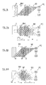
- Figures 3, 3A and 3B represent an exemplary embodiment of a system interferometric according to the invention making it possible to detect the characteristics of deep reflection of an object O.
- the system is said to be one-dimensional because it is able to collect measurement data only along a single Z axis supposed to cross the object. That is to say in the example, the measurement data are recorded in five points z0 to z4, point z0 being located for example on the front face, and point z4 on the back face of the object. Intermediate points z1, z2 and z3 can be representative of other places in the object where the reflective characteristics can translate its structure properties for example. The measurement record can thus inform the observer on typical characteristics of the object.
- the number of measurement points is only indicative, the system that can simultaneously capture many more points at a time, for example points z0 to zn.
- the number five was therefore chosen only to simplify the drawings.
- the interferometric device also includes a broadband and therefore low light source S consistency length.
- this SC source includes a superluminescent diode emitting on a 850 nm wavelength with a bandwidth of 20 nm.
- the source may also include an optical fiber single mode at 850 nm (not shown), to ensure that the beam is emitted in a single spatial mode.
- the device also includes a separator of beam SF, reference means M and means PC photosensors. These components are arranged in the same way so that in Figure 1, depending on the layout Michelson interferometric.
- the arms BM and BD are aligned on the Z axis and the arms BR and BS are aligned on a Y axis perpendicular to the Z axis and located in the same plane as this one (which is assumed to be the plane of the drawing in Figure 3).
- Y axes and Z intersect at the central point OC of the system.
- An axe X is defined perpendicular to this plane.
- the reference means M include a mirror having a plurality of mirrors elementary M0 to M4, here five in number, and arranged on a single optical unit presenting steps whose active faces are arranged perpendicular to the Y axis and parallel to the X axis.
- the means of reference M include as many steps as points of measure that we want to obtain along the Z axis in the object O. The steps thus define in the reference arm BR as many elementary reference beams FR0 to FR4 with different path lengths.
- the photosensor means PCs include a row of photosensor elements PC0 to PC4, here also five, the number depending the number of measurement points that we want to define in depth in object O. Note that the elements photosensors PC0 to PC4 are arranged side by side in their row parallel to the Y axis.
- the system interferometric includes a set of lenses L1 to L4 (see in particular Figures 3A and 3B).
- a first L1 of these lenses is collimator and provided in the source arm BS. It is placed in front of the source S and intended to form an image of it on the face of object O using lens L3 and on all the steps M0 to M4 of the reference means M using the L2 lens.
- the distance of lens L1 from the source S is preferably less than its distance focal in order to defocus the light spot on the object O and on the reference means M, in order to clarify the object O and the set of reference means M.
- the lenses L2, L3 and L4 form, with the SF separator, optical recombination means. They are determined in such a way that both each element photosensor PC0 to PC4 receives light from a position (xi, yi) of the object O via the object beam FO and that furthermore each photosensor element PC0 to PC4 does not receives light only from one level M0 to M4 from means of reference M.
- the couple of lenses L2, L4 located respectively in the arm of reference BR and in the detection arm BD projects a image of the reference means M on the elements photosensors PC0 to PC4 at the rate of one step per element photosensor.
- the pair of lenses L3, L4 located respectively in the BM measuring arm and the arm detection system projects an image of the object O onto all the photosensors PC0 to PC4.
- the focal lengths of L3 and L4 lenses will preferably be chosen so that f3 ⁇ f4, which will provide a resolution favorable in the direction of the X axis and the Y axis.
- elementary reference beams FR0 to FR4 and the beam FO thus projected interfere with each other others, so as to form an interference image which is received by the photosensors (PC0 to PC4).
- lenses L1 to L4 can be lenses spherical, preferably achromatic.
- the lenses could be replaced by light guides appropriate.
- the interferometric system according to the invention allows, with a single row of photosensors, to obtain by a single measurement instantaneous data per point in depth of the object (point z0 to z4) respectively at the rate of a given by photosensor element.
- the signals collected on the photosensor elements P0 to P4 can be used in processing them in the MA operating system, according to the results that we ultimately want to achieve, certain ways of treating them being described by the after.
- Figure 4 shows a sketch of a second exemplary embodiment of the invention in which the interferometric system is of the two-dimensional type.
- direction X In others terms, it becomes possible to collect data on a "slice" of the object indicated by oblique lines on FIG. 4 in order to release optical data according to a profile.
- FIGS. 5A to 8B make it possible to analyze according to a representation aligned the arms of the device interferometric respectively seen in elevation and in plan, according to figure 4.
- the figures show the lengths focal lengths of lenses L1 to L4 and their general shapes as well as the general path of the beams. For which relates to FIGS. 7A to 8B, only a few beams so as not to overload the figures.
- These figures also show that a diaphragm D can be placed in the detection arm BD next to the separator SF. The opening of this diaphragm is chosen in such a way that the spot of light that arrives on the surface of a photosensor stays inside a single cone of diffraction. This condition guarantees detection optimal interference fringes.
- Such a diaphragm can also be used in the figure interferometer 3, as shown.
- Figures 5A to 8B also show benchmarks identifying object points and photosensors correspondents with the identification of steps Z0 to Z4 reference means M.
- the number of measurement points in depth can be much greater than five (from z0 to zn), as well as the number of points in height according to the direction X (from x0 to xm).
- Figure 9 is a schematic representation of a example of arrangement of rotated PC photosensor means to the SF separator, according to one embodiment particularly interesting of the invention. Indeed, according to a particularly advantageous characteristic of the invention it is possible to extend the device two-dimensional interferometric to a device three-dimensional by means of two extremely additions simple.
- a plurality is provided here of matrices identified by the references y0 to yp and of place these matrices side by side along the Y axis of the device.
- a plurality of reference means placed side by side along the Z axis of the device.
- each of the matrices of photosensor elements will receive the image of a plan of reflection of the object, the planes being arranged in parallel one behind the other along the Z axis.
- PC means optical data in a volume of the object O and this, instantly without any mechanical manipulation spread out in time is not necessary.
- the measurement time does will be determined only by how quickly the electronic means of MA analysis.
- memory means for recording the data supplied by the PC photosensors before we start electronic analysis So it doesn't matter if the object is subject to movement, the acquisition time of the means photosensors and the memory being almost snapshots. This also applies equally to one-dimensional and two-dimensional embodiments.
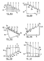
- Figure 10A shows a first possible variant reference means M in which these are formed by a plurality of mirrors 1a to 1n superimposed and offset, the step ⁇ z between two adjacent measurable points in depth being determined by the thickness hl of the mirrors elementary 1a to 1n.
- Figure 10B shows a second variant in which the reference means M comprise a network of diffraction with notches 2 (called “blazed grating”) in the Anglo-Saxon literature) whose angle ⁇ 1 defines the angle (“blazed angle”) and whose dimension h2 of the notches 2a to 2n defines the step ⁇ z which is the optical distance between two adjacent points measurable in depth in the object O.
- the reference means M comprise a network of diffraction with notches 2 (called “blazed grating") in the Anglo-Saxon literature) whose angle ⁇ 1 defines the angle (“blazed angle”) and whose dimension h2 of the notches 2a to 2n defines the step ⁇ z which is the optical distance between two adjacent points measurable in depth in the object O.
- blazed grating a network of diffraction with notches 2
- the reference means comprise a matrix 3 of retroreflectors 3a to 3n, (called “corner cubes” in Anglo-Saxon literature) in the shape of pyramids with a rectangular base.
- the angle ⁇ 2 defines the inclination of the plane of the bases of retroreflectors from the perpendicular direction to elementary beams.
- the dimension h3 indicates the pitch ⁇ z.
- FIG. 10D shows another form in which the reference means can be produced.
- a block 4 in a transparent medium is cut in "staircase" on its rear face, reflective deposits facing the opposite face of the block 4 being made on the steps 4a to 4n thus obtained.
- These steps form light coming from the source S as many elementary reference beams.
- the advantage of this variant is that it allows, by choosing a material with a refractive index n close to that of the object O, to reduce the loss in resolution due to the scattering of light in the reference arms and measurement of the interferometer.
- FIG. 10E takes the form of that of FIG. 10B. It includes a block 5 whose rungs are coated with reflective deposits 5a to 5n.
- the reflection coefficients Ra to Rn of these deposits are chosen according to the local nature of the points in depth of the object to be examined.
- An application example such reference means is encountered for example, for in-depth examination of the eye including the retina and cornea have very high reflection coefficients dissimilar, differences that these benchmarks allow to compensate by choosing coefficients of reflection determined for deposits.
- FIG. 10F represents a variant of means of benchmarks that operate by transparency.
- a block 6 in a transparent medium is cut in steps to form steps 6a to 6n.
- This block is placed in alignment of the source S and behind its opposite face is arranged a flat reflecting surface 7.
- the pitch of depth ⁇ z is equal to that of the variant in the figure 10D.
- Block 6 can also be used in a realization of the interferometric device according to the invention in which the reference means M and beams of light pass through the object.
- a variant of such a device is shown in the figure 11 which does not require further comments except that the results obtained are similar to those described in reference to Figures 3, 4 and 9, respectively.
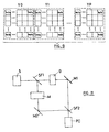
- Mach-Zehnder type interferometers well known to specialists. It includes two beam splitters SF1 and SF2 and two deflection mirrors M1 and M2.
- the step ⁇ z corresponding to an interference fringe is related to the wavelength of the source and is equal to ⁇ / 2.
- FIG. 12 illustrates an analysis direct signals obtained which can be executed by the MA analysis means.
- a maximum may not coincide with a photodetector element of the matrix.
- phase shifter or a phase modulator either in the BM measurement arm, ie in the reference arm BR.
- This phase shifter or phase modulator can be a cell with liquid crystal for example controlled by a voltage electric. It is schematically dotted in DPH on the figure 4, but it can also be provided in the interferometer in Figure 3.
- a picture is acquired on the matrix of PC photosensor elements. Then, a phase shift is produced by applying the voltage electric to the phase-shifter or DPH phase modulator. A new image is acquired on the photosensor matrix PC. Then, the analysis means MA carry out a selective subtraction of signals obtained from two successive images.
- the means of analysis provide a nonzero signal only at locations Z where there are interference. This method allows you to view the interference fringes but not necessarily getting the maximum intensity of a fringe.
- the difference between the optical length during the first measurement and that resulting from the phase shift must be chosen different from a multiple of 2 ⁇ .
- This method allows to use only 2 to 3 detectors by group of interference fringes, it being understood that the length (spatial spread) of a group of fringes is determined by the coherence length Lc of the source S. However, it requires two successive measurements, it is true very close together over time.
- the amplitude of an interference fringe can also be detected by time sampling.
- the phase shifter or phase modulator DPH is also provided, either in the reference arm BR or in the measurement arm BM.
- the value of the phase is taken with respect to the mean wavelength of the source S.
- I o [ ⁇ i I i - I avg 2 ] 1 2 .
- the three analysis methods which have just been have the advantage of allowing the use of standard photosensor arrays, such as a camera CCD, APS active matrices etc.
- the DPH phase shifter or phase modulator can be used to modulate the phase of the light either in the measuring arm, either in the reference arm of a periodically, for example sinusoidal.
- the analysis means are advantageously carried out according to the method described in the article by Swanson et al. appeared in "Optics Letters" Jan. 15, 1992, Vol 17, no 2.
- the source S can be unique as described so far. However, it is also possible to use a line sources, even a matrix. As a result, more of light energy becomes available per element photosensor, which provides a better ratio signal / noise.
- each beam illuminates a position along the X axis of the sample and illuminates all elementary mirrors z0 to zn means of reference.
- Each beam of the BM measuring arm is recombined with its series of reference arm beams BR.
- each line of n beams of sources illuminates a position according to the X axis of the object O and illuminates all the positions z0 to zn (along the Z axis) of the reference means, at the rate of a elementary source by position.
- Each beam of the arm of BM measurement is recombined with its reference beam associated.
- Suitable light sources are diodes side-emitting electroluminescent, laser diodes, stacks of laser diode arrays or diodes or arrays of laser diodes with vertical cavities.
- Diodes electroluminescent or other sources emitting non-coherent light (tungsten filament) can also be used with circular diaphragms or rectangular.
Landscapes
- Physics & Mathematics (AREA)
- General Physics & Mathematics (AREA)
- Instruments For Measurement Of Length By Optical Means (AREA)
- Length Measuring Devices By Optical Means (AREA)
- Investigating Or Analysing Materials By Optical Means (AREA)
Applications Claiming Priority (2)
| Application Number | Priority Date | Filing Date | Title |
|---|---|---|---|
| FR9811311 | 1998-09-10 | ||
| FR9811311A FR2783323B1 (fr) | 1998-09-10 | 1998-09-10 | Dispositif interferometrique pour relever les caracteristiques de reflexion et/ou de transmission optiques en profondeur d'un objet |
Publications (2)
| Publication Number | Publication Date |
|---|---|
| EP0985902A1 true EP0985902A1 (de) | 2000-03-15 |
| EP0985902B1 EP0985902B1 (de) | 2004-11-24 |
Family
ID=9530303
Family Applications (1)
| Application Number | Title | Priority Date | Filing Date |
|---|---|---|---|
| EP99402227A Expired - Lifetime EP0985902B1 (de) | 1998-09-10 | 1999-09-10 | Interferometrische Vorrichtung zum Sichtbarmachung von Optischen Reflexion- und/oder Transmissionscharakteristiken im inneren eines Objektes |
Country Status (4)
| Country | Link |
|---|---|
| US (1) | US6268921B1 (de) |
| EP (1) | EP0985902B1 (de) |
| DE (1) | DE69922109T2 (de) |
| FR (1) | FR2783323B1 (de) |
Families Citing this family (45)
| Publication number | Priority date | Publication date | Assignee | Title |
|---|---|---|---|---|
| DE19929406A1 (de) * | 1999-06-26 | 2000-12-28 | Zeiss Carl Fa | Zeilen-OCT als optischer Sensor für die Meß- und Medizintechnik |
| US6411638B1 (en) * | 1999-08-31 | 2002-06-25 | Honeywell Inc. | Coupled cavity anti-guided vertical-cavity surface-emitting laser |
| US20070221265A1 (en) * | 2006-03-22 | 2007-09-27 | Sion Power Corporation | Rechargeable lithium/water, lithium/air batteries |
| WO2002071042A2 (en) * | 2001-01-29 | 2002-09-12 | Izatt Joseph A | Frequency-encoded parallel oct and associated systems and methods |
| DE10142001A1 (de) * | 2001-08-28 | 2003-03-20 | Zeiss Carl Jena Gmbh | Optische Multiplex Kurzkohärenz-Interferometrie am Auge |
| US8968279B2 (en) * | 2003-03-06 | 2015-03-03 | Amo Manufacturing Usa, Llc | Systems and methods for qualifying and calibrating a beam delivery system |
| US7092101B2 (en) * | 2003-04-16 | 2006-08-15 | Duke University | Methods and systems for static multimode multiplex spectroscopy |
| GB2406638B (en) * | 2003-10-01 | 2006-03-29 | Amc Amsterdam | Interferometric measurement apparatus and method therefor |
| JP4409331B2 (ja) * | 2004-03-30 | 2010-02-03 | 株式会社トプコン | 光画像計測装置 |
| TWI245926B (en) * | 2004-05-10 | 2005-12-21 | Chroma Ate Inc | Device and method of an interference scanner |
| US7242480B2 (en) * | 2004-05-14 | 2007-07-10 | Medeikon Corporation | Low coherence interferometry for detecting and characterizing plaques |
| US20050254059A1 (en) * | 2004-05-14 | 2005-11-17 | Alphonse Gerard A | Low coherence interferometric system for optical metrology |
| US7327463B2 (en) | 2004-05-14 | 2008-02-05 | Medrikon Corporation | Low coherence interferometry utilizing magnitude |
| US7190464B2 (en) * | 2004-05-14 | 2007-03-13 | Medeikon Corporation | Low coherence interferometry for detecting and characterizing plaques |
| US7184148B2 (en) | 2004-05-14 | 2007-02-27 | Medeikon Corporation | Low coherence interferometry utilizing phase |
| US7474408B2 (en) * | 2004-05-14 | 2009-01-06 | Medeikon Corporation | Low coherence interferometry utilizing phase |
| DE102004037479A1 (de) | 2004-08-03 | 2006-03-16 | Carl Zeiss Meditec Ag | Fourier-Domain OCT Ray-Tracing am Auge |
| DE102004045802B4 (de) * | 2004-09-22 | 2009-02-05 | Robert Bosch Gmbh | Interferometrisches System mit Referenzfläche mit einer verspiegelten Zone |
| EP1805480B1 (de) * | 2004-10-29 | 2009-01-14 | DeguDent GmbH | Verfahren und vorrichtung zur erfassung von konturdaten und/oder optischen eigenschaften eines dreidimensionalen semitransparenten objekts |
| WO2006128442A1 (de) * | 2005-05-31 | 2006-12-07 | W.O.M. World Of Medicine Ag | Verfahren und vorrichtung zur optischen charakterisierung von gewebe |
| US7811280B2 (en) | 2006-01-26 | 2010-10-12 | Amo Manufacturing Usa, Llc. | System and method for laser ablation calibration |
| GB2435322A (en) * | 2006-02-15 | 2007-08-22 | Oti Ophthalmic Technologies | Measuring curvature or axial position using OCT |
| US7488930B2 (en) * | 2006-06-02 | 2009-02-10 | Medeikon Corporation | Multi-channel low coherence interferometer |
| EP1939581A1 (de) | 2006-12-27 | 2008-07-02 | Heliotis AG | Vorrichtung zur kontaktlosen interferometrischen Bestimmung von Oberflächenhöhenprofilen und Tiefenstreuungsprofilen |
| EP2128588B1 (de) * | 2007-02-28 | 2013-04-10 | Nippon Telegraph and Telephone Corporation | Verfahren und vorrichtung für optische refraktometrie |
| DE102007023293B3 (de) * | 2007-05-16 | 2008-09-25 | Universität Zu Lübeck | Verfahren zur Optischen Kohärenztomographie |
| KR101029606B1 (ko) * | 2007-10-19 | 2011-05-09 | 주식회사 엠티씨메디칼 | 광간섭 결맞음 단층촬영장치 |
| US10426348B2 (en) | 2008-03-05 | 2019-10-01 | Purdue Research Foundation | Using differential time-frequency tissue-response spectroscopy to evaluate living body response to a drug |
| JP5740701B2 (ja) * | 2009-03-30 | 2015-06-24 | 国立大学法人埼玉大学 | 干渉計 |
| DE102009022598A1 (de) | 2009-05-20 | 2010-11-25 | Carl Zeiss Meditec Ag | Verfahren zur Bestimmung absoluter Messwerte eines Auges |
| DE102009053006B4 (de) * | 2009-11-16 | 2014-04-24 | Bundesrepublik Deutschland, vertr.d.d. Bundesministerium für Wirtschaft und Technologie, d.vertr.d.d. Präsidenten der Physikalisch-Technischen Bundesanstalt | Längenmessgerät |
| TWI480513B (zh) | 2009-12-04 | 2015-04-11 | Raydium Semiconductor Corp | 光學同調斷層檢測裝置及其運作方法 |
| EP2565621A4 (de) * | 2010-03-17 | 2018-03-14 | National University Corporation Saitama University | Vorrichtung zur messung des spektrums eines elektrischen feldes und objektmessvorrichtung |
| US9977859B2 (en) * | 2010-06-17 | 2018-05-22 | Purdue Reserach Foundation | Digital holographic method of measuring cellular activity and of using results to screen compounds |
| US10401793B2 (en) | 2010-06-17 | 2019-09-03 | Purdue Research Foundation | Digital holographic method of measuring cellular activity and measuring apparatus with improved stability |
| US20120086948A1 (en) * | 2010-10-08 | 2012-04-12 | Electronics And Telecommunications Research Institute | Optical coherence tomography apparatus for enhanced axial contrast and reference mirror having multiple planes for the same |
| DE102010051281A1 (de) | 2010-11-12 | 2012-05-16 | Carl Zeiss Meditec Ag | Verfahren zur modellbasierten Bestimmung der Biometrie von Augen |
| JP5743697B2 (ja) * | 2011-05-06 | 2015-07-01 | キヤノン株式会社 | 計測装置 |
| WO2013116516A1 (en) | 2012-02-03 | 2013-08-08 | Wayne State University | Fourier-transform interferometer with staircase reflective element |
| WO2014018140A2 (en) | 2012-04-23 | 2014-01-30 | Wayne State University | Static interferometer with step-style reflective element |
| JP2015017966A (ja) * | 2013-06-13 | 2015-01-29 | キヤノン株式会社 | 撮像装置および撮像方法 |
| CN104006885B (zh) * | 2014-03-10 | 2016-08-17 | 中国科学院长春光学精密机械与物理研究所 | 时空联合调制傅里叶变换成像光谱仪及制作方法 |
| EP3117191A4 (de) * | 2014-03-13 | 2018-03-28 | National University of Singapore | Optische interferenzvorrichtung |
| JP2017067742A (ja) * | 2015-10-02 | 2017-04-06 | レーザーテック株式会社 | 干渉計及び変位量測定装置 |
| US20210263295A1 (en) * | 2020-02-25 | 2021-08-26 | The Board Of Regents Of The University Of Texas System | Imaging system and method to convert lateral scanning into axial remote focusing |
Citations (5)
| Publication number | Priority date | Publication date | Assignee | Title |
|---|---|---|---|---|
| US4309109A (en) * | 1972-05-25 | 1982-01-05 | The United States Of America As Represented By The Secretary Of The Navy | Pulsed interferometric remote gauge |
| US5151585A (en) * | 1991-08-12 | 1992-09-29 | Hughes Danbury Optical Systems, Inc. | Coherent radiation detector |
| US5239364A (en) * | 1990-10-26 | 1993-08-24 | Olympus Optical Co., Ltd. | Light phase difference measuring method using an interferometer |
| WO1994018523A1 (en) * | 1993-02-01 | 1994-08-18 | Zygo Corporation | Method and apparatus for the rapid acquisition of data in coherence scanning interferometry |
| WO1995024621A1 (en) * | 1994-03-09 | 1995-09-14 | The Secretary Of State For Defence | Coherence imaging system |
Family Cites Families (4)
| Publication number | Priority date | Publication date | Assignee | Title |
|---|---|---|---|---|
| FR2658460B1 (fr) | 1990-02-22 | 1994-12-02 | Valeo Systemes Dessuyage | Dispositif d'essuie-glace, notamment pour pare-brise de vehicule. |
| DE4234202C2 (de) | 1992-10-10 | 1995-06-14 | Teves Gmbh Alfred | Vorrichtung zum Reinigen von Windschutzscheiben |
| JPH10267830A (ja) * | 1997-03-26 | 1998-10-09 | Kowa Co | 光学測定装置 |
| US5892583A (en) * | 1997-08-21 | 1999-04-06 | Li; Ming-Chiang | High speed inspection of a sample using superbroad radiation coherent interferometer |
-
1998
- 1998-09-10 FR FR9811311A patent/FR2783323B1/fr not_active Expired - Fee Related
-
1999
- 1999-09-10 DE DE69922109T patent/DE69922109T2/de not_active Expired - Lifetime
- 1999-09-10 EP EP99402227A patent/EP0985902B1/de not_active Expired - Lifetime
- 1999-09-10 US US09/394,543 patent/US6268921B1/en not_active Expired - Lifetime
Patent Citations (5)
| Publication number | Priority date | Publication date | Assignee | Title |
|---|---|---|---|---|
| US4309109A (en) * | 1972-05-25 | 1982-01-05 | The United States Of America As Represented By The Secretary Of The Navy | Pulsed interferometric remote gauge |
| US5239364A (en) * | 1990-10-26 | 1993-08-24 | Olympus Optical Co., Ltd. | Light phase difference measuring method using an interferometer |
| US5151585A (en) * | 1991-08-12 | 1992-09-29 | Hughes Danbury Optical Systems, Inc. | Coherent radiation detector |
| WO1994018523A1 (en) * | 1993-02-01 | 1994-08-18 | Zygo Corporation | Method and apparatus for the rapid acquisition of data in coherence scanning interferometry |
| WO1995024621A1 (en) * | 1994-03-09 | 1995-09-14 | The Secretary Of State For Defence | Coherence imaging system |
Non-Patent Citations (1)
| Title |
|---|
| E.A. SWANSON: "IN VIVO RETINAL IMAGING BY OPTICAL COHERENCE TOMOGRAPHY", OPTICS LETTERS, vol. 18, no. 21, 1 November 1993 (1993-11-01), pages 1864 - 1866, XP002102402 * |
Also Published As
| Publication number | Publication date |
|---|---|
| EP0985902B1 (de) | 2004-11-24 |
| FR2783323B1 (fr) | 2000-10-13 |
| DE69922109D1 (de) | 2004-12-30 |
| DE69922109T2 (de) | 2005-12-01 |
| FR2783323A1 (fr) | 2000-03-17 |
| US6268921B1 (en) | 2001-07-31 |
Similar Documents
| Publication | Publication Date | Title |
|---|---|---|
| EP0985902B1 (de) | Interferometrische Vorrichtung zum Sichtbarmachung von Optischen Reflexion- und/oder Transmissionscharakteristiken im inneren eines Objektes | |
| EP3084345B1 (de) | Optische tomographievorrichtung und verfahren | |
| EP3394560A1 (de) | Vorrichtung und verfahren zur messung der höhe in gegenwart von dünnschichten | |
| EP1364181B1 (de) | Verfahren und einrichtung zur schnellen interferenziellen mikroskopischen abbildung eines objekts | |
| EP3980715A1 (de) | Verfahren und vorrichtung zum messen von schnittstellen eines optischen elements | |
| FR2726641A1 (fr) | Procede et dispositif pour profiler des surfaces en utilisant une optique de diffraction | |
| EP0278882A1 (de) | Verfahren und Vorrichtung zum Erstellen eines Abdrucks für medizinische Zwecke | |
| FR2960291A1 (fr) | Methode et dispositif de microscopie interferentielle plein champ a haute resolution | |
| EP4042098A1 (de) | Vorrichtung und verfahren zur bildgebung und interferometrie | |
| EP2376882B1 (de) | Vorrichtung und verfahren zur bestimmung von polarisationsinformationen und polarimetrische bildgebungsvorrichtung | |
| WO2020178234A1 (fr) | Procede et dispositif de mesure d'interfaces d'un element optique | |
| WO2018189250A1 (fr) | Systeme et procede de metrologie optique plein champ en super resolution a l'echelle nanometrique en champ lointain | |
| WO2022058236A1 (fr) | Dispositif et procédé de mesure d'interfaces d'un élément optique | |
| EP3491330B1 (de) | Interferenzielle vollfeldbildgebungssysteme und verfahren | |
| FR2707018A1 (de) | ||
| EP3602201A1 (de) | Vorrichtungen und verfahren zur optischen bildgebung mittels digitaler holographie ausserhalb der achse | |
| FR3075463A1 (fr) | Capteur d'image, permettant d'obtenir une information relative a la phase d'une onde lumineuse. | |
| FR3064760A1 (fr) | Interferometre holographique numerique a deux faisceaux de reference pour analyser un milieu transparent | |
| EP3601946B1 (de) | Verfahren und vorrichtung zur kurzkohärenten reflektometrie unter verwendung von zeit-frequenz-erfassung | |
| WO2011042674A1 (fr) | Procede et systeme d'analyse structurelle d'un objet par mesure de front d'onde | |
| FR2765964A1 (fr) | Dispositif optique de mesure de distance avec une grande precision | |
| FR2584811A1 (fr) | Dispositif de mesure de deformations d'un corps, notamment d'une maquette en soufflerie aerodynamique | |
| FR3128013A1 (fr) | Procédé et dispositif de mesure d’interfaces d’un élément optique | |
| WO2023156519A1 (fr) | Systèmes et procédés d'analyse de la qualité de surface d'une lame à faces parallèles | |
| WO2003002989A1 (fr) | Microscope pour la tomographie optique coherente |
Legal Events
| Date | Code | Title | Description |
|---|---|---|---|
| PUAI | Public reference made under article 153(3) epc to a published international application that has entered the european phase |
Free format text: ORIGINAL CODE: 0009012 |
|
| AK | Designated contracting states |
Kind code of ref document: A1 Designated state(s): CH DE FR GB LI |
|
| AX | Request for extension of the european patent |
Free format text: AL;LT;LV;MK;RO;SI |
|
| RIN1 | Information on inventor provided before grant (corrected) |
Inventor name: SALATHE, RENE-PAUL Inventor name: BOURQUIN, STEPHANE Inventor name: SEITZ, PETER |
|
| 17P | Request for examination filed |
Effective date: 20000912 |
|
| AKX | Designation fees paid |
Free format text: CH DE FR GB LI |
|
| 17Q | First examination report despatched |
Effective date: 20030715 |
|
| GRAP | Despatch of communication of intention to grant a patent |
Free format text: ORIGINAL CODE: EPIDOSNIGR1 |
|
| GRAS | Grant fee paid |
Free format text: ORIGINAL CODE: EPIDOSNIGR3 |
|
| RAP1 | Party data changed (applicant data changed or rights of an application transferred) |
Owner name: CSEM CENTRE SUISSE D'ELECTRONIQUE ET DE MICROTECHN |
|
| GRAA | (expected) grant |
Free format text: ORIGINAL CODE: 0009210 |
|
| AK | Designated contracting states |
Kind code of ref document: B1 Designated state(s): CH DE FR GB LI |
|
| REG | Reference to a national code |
Ref country code: GB Ref legal event code: FG4D Free format text: NOT ENGLISH |
|
| REG | Reference to a national code |
Ref country code: CH Ref legal event code: EP |
|
| REF | Corresponds to: |
Ref document number: 69922109 Country of ref document: DE Date of ref document: 20041230 Kind code of ref document: P |
|
| GBT | Gb: translation of ep patent filed (gb section 77(6)(a)/1977) |
Effective date: 20050120 |
|
| PLBE | No opposition filed within time limit |
Free format text: ORIGINAL CODE: 0009261 |
|
| STAA | Information on the status of an ep patent application or granted ep patent |
Free format text: STATUS: NO OPPOSITION FILED WITHIN TIME LIMIT |
|
| 26N | No opposition filed |
Effective date: 20050825 |
|
| REG | Reference to a national code |
Ref country code: CH Ref legal event code: NV Representative=s name: GLN S.A. |
|
| PGFP | Annual fee paid to national office [announced via postgrant information from national office to epo] |
Ref country code: GB Payment date: 20110926 Year of fee payment: 13 Ref country code: FR Payment date: 20111005 Year of fee payment: 13 |
|
| REG | Reference to a national code |
Ref country code: CH Ref legal event code: PCAR Free format text: NEW ADDRESS: AVENUE EDOUARD-DUBOIS 20, 2000 NEUCHATEL (CH) |
|
| GBPC | Gb: european patent ceased through non-payment of renewal fee |
Effective date: 20120910 |
|
| REG | Reference to a national code |
Ref country code: FR Ref legal event code: ST Effective date: 20130531 |
|
| PG25 | Lapsed in a contracting state [announced via postgrant information from national office to epo] |
Ref country code: GB Free format text: LAPSE BECAUSE OF NON-PAYMENT OF DUE FEES Effective date: 20120910 |
|
| PG25 | Lapsed in a contracting state [announced via postgrant information from national office to epo] |
Ref country code: FR Free format text: LAPSE BECAUSE OF NON-PAYMENT OF DUE FEES Effective date: 20121001 |
|
| PGFP | Annual fee paid to national office [announced via postgrant information from national office to epo] |
Ref country code: DE Payment date: 20140929 Year of fee payment: 16 |
|
| PGFP | Annual fee paid to national office [announced via postgrant information from national office to epo] |
Ref country code: CH Payment date: 20150928 Year of fee payment: 17 |
|
| REG | Reference to a national code |
Ref country code: DE Ref legal event code: R119 Ref document number: 69922109 Country of ref document: DE |
|
| PG25 | Lapsed in a contracting state [announced via postgrant information from national office to epo] |
Ref country code: DE Free format text: LAPSE BECAUSE OF NON-PAYMENT OF DUE FEES Effective date: 20160401 |
|
| REG | Reference to a national code |
Ref country code: CH Ref legal event code: PFA Owner name: CSEM CENTRE SUISSE D'ELECTRONIQUE ET DE MICROT, CH Free format text: FORMER OWNER: CSEM CENTRE SUISSE D'ELECTRONIQUE ET DE MICROTECHNIQUE SA -RECHERCHE ET DEVELOPPEMENT, CH |
|
| REG | Reference to a national code |
Ref country code: CH Ref legal event code: PL |
|
| PG25 | Lapsed in a contracting state [announced via postgrant information from national office to epo] |
Ref country code: CH Free format text: LAPSE BECAUSE OF NON-PAYMENT OF DUE FEES Effective date: 20160930 Ref country code: LI Free format text: LAPSE BECAUSE OF NON-PAYMENT OF DUE FEES Effective date: 20160930 |