EP0802637A1 - Communication device - Google Patents
Communication device Download PDFInfo
- Publication number
- EP0802637A1 EP0802637A1 EP96935547A EP96935547A EP0802637A1 EP 0802637 A1 EP0802637 A1 EP 0802637A1 EP 96935547 A EP96935547 A EP 96935547A EP 96935547 A EP96935547 A EP 96935547A EP 0802637 A1 EP0802637 A1 EP 0802637A1
- Authority
- EP
- European Patent Office
- Prior art keywords
- communication apparatus
- circuit board
- sensitivity
- disposed
- board
- Prior art date
- Legal status (The legal status is an assumption and is not a legal conclusion. Google has not performed a legal analysis and makes no representation as to the accuracy of the status listed.)
- Granted
Links
Images


Classifications
-
- H—ELECTRICITY
- H04—ELECTRIC COMMUNICATION TECHNIQUE
- H04B—TRANSMISSION
- H04B1/00—Details of transmission systems, not covered by a single one of groups H04B3/00 - H04B13/00; Details of transmission systems not characterised by the medium used for transmission
- H04B1/38—Transceivers, i.e. devices in which transmitter and receiver form a structural unit and in which at least one part is used for functions of transmitting and receiving
- H04B1/3827—Portable transceivers
- H04B1/385—Transceivers carried on the body, e.g. in helmets
-
- H—ELECTRICITY
- H01—ELECTRIC ELEMENTS
- H01Q—ANTENNAS, i.e. RADIO AERIALS
- H01Q1/00—Details of, or arrangements associated with, antennas
- H01Q1/27—Adaptation for use in or on movable bodies
- H01Q1/273—Adaptation for carrying or wearing by persons or animals
-
- H—ELECTRICITY
- H01—ELECTRIC ELEMENTS
- H01Q—ANTENNAS, i.e. RADIO AERIALS
- H01Q7/00—Loop antennas with a substantially uniform current distribution around the loop and having a directional radiation pattern in a plane perpendicular to the plane of the loop
-
- H—ELECTRICITY
- H04—ELECTRIC COMMUNICATION TECHNIQUE
- H04B—TRANSMISSION
- H04B1/00—Details of transmission systems, not covered by a single one of groups H04B3/00 - H04B13/00; Details of transmission systems not characterised by the medium used for transmission
- H04B1/06—Receivers
- H04B1/10—Means associated with receiver for limiting or suppressing noise or interference
- H04B1/1009—Placing the antenna at a place where the noise level is low and using a noise-free transmission line between the antenna and the receivers
-
- H—ELECTRICITY
- H01—ELECTRIC ELEMENTS
- H01L—SEMICONDUCTOR DEVICES NOT COVERED BY CLASS H10
- H01L2223/00—Details relating to semiconductor or other solid state devices covered by the group H01L23/00
- H01L2223/58—Structural electrical arrangements for semiconductor devices not otherwise provided for
- H01L2223/64—Impedance arrangements
- H01L2223/66—High-frequency adaptations
- H01L2223/6661—High-frequency adaptations for passive devices
- H01L2223/6677—High-frequency adaptations for passive devices for antenna, e.g. antenna included within housing of semiconductor device
-
- H—ELECTRICITY
- H01—ELECTRIC ELEMENTS
- H01L—SEMICONDUCTOR DEVICES NOT COVERED BY CLASS H10
- H01L2224/00—Indexing scheme for arrangements for connecting or disconnecting semiconductor or solid-state bodies and methods related thereto as covered by H01L24/00
- H01L2224/01—Means for bonding being attached to, or being formed on, the surface to be connected, e.g. chip-to-package, die-attach, "first-level" interconnects; Manufacturing methods related thereto
- H01L2224/10—Bump connectors; Manufacturing methods related thereto
- H01L2224/15—Structure, shape, material or disposition of the bump connectors after the connecting process
- H01L2224/16—Structure, shape, material or disposition of the bump connectors after the connecting process of an individual bump connector
- H01L2224/161—Disposition
- H01L2224/16151—Disposition the bump connector connecting between a semiconductor or solid-state body and an item not being a semiconductor or solid-state body, e.g. chip-to-substrate, chip-to-passive
- H01L2224/16221—Disposition the bump connector connecting between a semiconductor or solid-state body and an item not being a semiconductor or solid-state body, e.g. chip-to-substrate, chip-to-passive the body and the item being stacked
- H01L2224/16225—Disposition the bump connector connecting between a semiconductor or solid-state body and an item not being a semiconductor or solid-state body, e.g. chip-to-substrate, chip-to-passive the body and the item being stacked the item being non-metallic, e.g. insulating substrate with or without metallisation
-
- H—ELECTRICITY
- H01—ELECTRIC ELEMENTS
- H01L—SEMICONDUCTOR DEVICES NOT COVERED BY CLASS H10
- H01L2224/00—Indexing scheme for arrangements for connecting or disconnecting semiconductor or solid-state bodies and methods related thereto as covered by H01L24/00
- H01L2224/01—Means for bonding being attached to, or being formed on, the surface to be connected, e.g. chip-to-package, die-attach, "first-level" interconnects; Manufacturing methods related thereto
- H01L2224/42—Wire connectors; Manufacturing methods related thereto
- H01L2224/47—Structure, shape, material or disposition of the wire connectors after the connecting process
- H01L2224/48—Structure, shape, material or disposition of the wire connectors after the connecting process of an individual wire connector
- H01L2224/4805—Shape
- H01L2224/4809—Loop shape
- H01L2224/48091—Arched
-
- H—ELECTRICITY
- H01—ELECTRIC ELEMENTS
- H01L—SEMICONDUCTOR DEVICES NOT COVERED BY CLASS H10
- H01L2224/00—Indexing scheme for arrangements for connecting or disconnecting semiconductor or solid-state bodies and methods related thereto as covered by H01L24/00
- H01L2224/01—Means for bonding being attached to, or being formed on, the surface to be connected, e.g. chip-to-package, die-attach, "first-level" interconnects; Manufacturing methods related thereto
- H01L2224/42—Wire connectors; Manufacturing methods related thereto
- H01L2224/47—Structure, shape, material or disposition of the wire connectors after the connecting process
- H01L2224/48—Structure, shape, material or disposition of the wire connectors after the connecting process of an individual wire connector
- H01L2224/481—Disposition
- H01L2224/48151—Connecting between a semiconductor or solid-state body and an item not being a semiconductor or solid-state body, e.g. chip-to-substrate, chip-to-passive
- H01L2224/48221—Connecting between a semiconductor or solid-state body and an item not being a semiconductor or solid-state body, e.g. chip-to-substrate, chip-to-passive the body and the item being stacked
- H01L2224/48225—Connecting between a semiconductor or solid-state body and an item not being a semiconductor or solid-state body, e.g. chip-to-substrate, chip-to-passive the body and the item being stacked the item being non-metallic, e.g. insulating substrate with or without metallisation
- H01L2224/48227—Connecting between a semiconductor or solid-state body and an item not being a semiconductor or solid-state body, e.g. chip-to-substrate, chip-to-passive the body and the item being stacked the item being non-metallic, e.g. insulating substrate with or without metallisation connecting the wire to a bond pad of the item
-
- H—ELECTRICITY
- H01—ELECTRIC ELEMENTS
- H01L—SEMICONDUCTOR DEVICES NOT COVERED BY CLASS H10
- H01L2924/00—Indexing scheme for arrangements or methods for connecting or disconnecting semiconductor or solid-state bodies as covered by H01L24/00
- H01L2924/0001—Technical content checked by a classifier
- H01L2924/00014—Technical content checked by a classifier the subject-matter covered by the group, the symbol of which is combined with the symbol of this group, being disclosed without further technical details
Definitions
- the present invention relates to communication apparatuses such as receivers and transmitters.
- the present invention more specifically relates to a technology for effectively reducing an effect of high-frequency noise generated by an integrated circuit (hereinafter called IC) in a communication apparatus, on an antenna body.
- IC integrated circuit
- a watch with an FM radio and a watch-shaped individual-selective-calling receiver have been known.
- an electrically conductive plate member or film is put in a watchband for mounting an apparatus body at a wrist. Therefore, when the watchband is mounted at the wrist, a loop antenna is formed by the plate member or film.
- the apparatus body includes a circuit board 73 on which a high-frequency analog IC 93B for transmission or receiving and a signal-processing digital IC 94B which is driven by a driving signal having a frequency as high as several MHz are mounted.
- These ICs are wire-bonded on the rear surface section 732 of the circuit board 73 at the rear surface side (side where the entire or most part of a loop antenna 4 is disposed) of the circuit board 73.
- a display digital IC 95B (indicated by C-IC in the figure) which is driven by a several-tens-of-kHz driving signal is mounted on the front surface section 721 of a circuit board 72 by wire bonding.
- the object of the present invention is achieved through the provision of a communication apparatus including a board on which an integrated circuit generating high-frequency noise is mounted; and an antenna body the entire or most of which is disposed on one board-surface side of the board, wherein the integrated circuit is mounted on the board such that the active surface thereof directs at the direction opposite the direction where the entire or most of the antenna body is disposed against the board.
- a communication apparatus since the active surface of an integrated circuit generating high-frequency noise directs at the direction opposite the direction where the entire or most of the antenna body is disposed, even if the integrated circuit emits high-frequency noise from its active surface, the high-frequency noise unlikely reaches the antenna body. Therefore, the sensitivity of the communication apparatus can be increased.
- the communication apparatus is, for example, provided with an apparatus body in which a side on which a display screen is formed is set to a front surface side and a watchband extending from the apparatus body toward the rear surface side for mounting the apparatus body to the wrist, and the antenna body is formed in the watchband, and the board is disposed at the rear surface side of the display screen in the apparatus body.
- an integrated circuit generating the high-frequency noise includes, for example, a high-frequency analog integrated circuit having at least one of functions between a transmission function and a receiving function, a signal-processing digital integrated circuit driven by a high-frequency driving signal, or a CPU.
- the integrated circuit is, for example, face-down-bonded to a board surface where the entire or most of the antenna body is disposed in the board.
- the integrated circuit may be wire-bonded to the board surface opposite the surface where the entire or most of the antenna body is disposed in the board so that the active surface of the integrated circuit directs at the direction opposite the direction where the entire or most of the antenna body is disposed against the board.
- face-down bonding means all methods for electrically connecting electrodes by adhering a surface electrode or a Wiring lead mounted in advance on a semiconductor chip for an integrated circuit to a wiring electrode formed on a board with both front surfaces thereof facing each other, and includes flip-chip bonding.
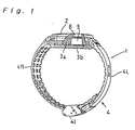
- Fig. 1 is a view indicating the entire structure of a wrist-mount-type communication apparatus according to an embodiment of the present invention.
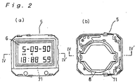
- Fig. 2(a) is a plan of a circuit assembly mounted on the wrist-mount-type communication apparatus shown in Fig. 1.
- Fig. 2(b) is a bottom view thereof.
- Fig. 3(a) is a view typically indicating a cross section taken on line IV-IV' of the circuit assembly according to embodiment 1 shown in Fig. 2.
- Fig. 3(b) is a view typically indicating a cross section taken on a position corresponding to line IV-IV' shown in Fig. 2 of a circuit assembly according to a comparison case.
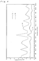
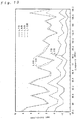
- Fig. 4 is a graph indicating a comparison between the sensitivity characteristics of a wrist-mount-type communication apparatus using the structure according to embodiment 1 shown in Fig. 3(a) and the sensitivity characteristics of a wrist-mount-type communication apparatus using the structure according to the comparison case shown in Fig. 3(b).
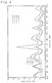
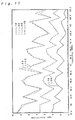
- Fig. 5 is a graph indicating the sensitivity characteristics of a wrist-mount-type communication apparatus using the structure according to embodiment 1 shown in Fig. 3(a), with assembly conditions being changed.
- Fig. 6 is a graph indicating the sensitivity characteristics of a wrist-mount-type communication apparatus using the structure according to the comparison case shown in Fig. 3(b), with assembly conditions being changed.
- Fig. 7 is a graph indicating the sensitivity characteristics of a wrist-mount-type communication apparatus using the structure according to embodiment 1 shown in Fig. 3(a), with assembly conditions being changed and with a sample other than that used in evaluation shown in Fig. 5.
- Fig. 8 is a graph indicating the sensitivity characteristics of a wrist-mount-type communication apparatus using the structure according to the comparison case shown in Fig. 3(b), with assembly conditions being changed and with a sample other than that used in evaluation shown in Fig. 6.
- Fig. 9(a) is a view typically indicating a cross section taken on line IV-IV' of a circuit assembly according to embodiment 2 shown in Fig. 2.
- Fig. 9(b) is a view typically indicating a cross section taken on a position corresponding to line IV-IV' of a circuit assembly according to a conventional case.
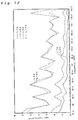
- Fig. 10 is a graph indicating the sensitivity characteristics of a wrist-mount-type communication apparatus using the structure according to embodiment 2 shown in Fig. 9(a), with assembly conditions being changed.
- Fig. 11 is a graph indicating the sensitivity characteristics of a wrist-mount-type communication apparatus using the structure according to the conventional case shown in Fig. 9(b), with assembly conditions being changed.
- Fig. 12 is a graph indicating the sensitivity characteristics of a wrist-mount-type communication apparatus using the structure according to embodiment 2 shown in Fig. 9(a), with assembly conditions being changed and with a sample other than that used in evaluation shown in Fig. 10.
- Fig. 13 is a graph indicating the sensitivity characteristics of a wrist-mount-type communication apparatus using the structure according to the conventional case shown in Fig. 9(b), with assembly conditions being changed and with a sample other than that used in evaluation shown in Fig. 11.
- Fig. 14(a) is a perspective view typically showing arrangement of an antenna body and a circuit board in a communication apparatus according to embodiment 3.
- Fig. 14(b) is a side view of the structure.
- Fig. 15(a) is a perspective view typically showing arrangement of an antenna body and a circuit board in a communication apparatus according to embodiment 4.
- Fig. 15(b) is a side view of the structure.
- Fig. 1 is a view indicating a configuration of a wrist-mount-type communication apparatus to which the present invention is applied.
- the wrist-mount type communication apparatus 1 is formed by an apparatus body 2 which has a liquid crystal display panel 6 (display screen) disposed on the front surface side thereof and a pair of watchbands 4R and 4L.
- a liquid crystal display panel 6 display screen
- Each of the watchbands 4R and 4L is mounted to both ends of the apparatus body at each watchband main end.
- These wrist bands can be connected to each other at each sub end by a buckle 41.
- the watchbands 4R and 4L are provided with electrically conductive plates thereinside and mounted at the wrist of the user. When the sub ends of the watchbands 4R and 4L are connected, they form a loop antenna 4 (antenna body).
- the apparatus body 2 is formed by a front-surface-side casing 3a and a rear cover 3b secured to the rear side of the casing 3a at the rear side of the apparatus body 2.
- a circuit assembly 5 is built in the apparatus body 2, which is formed by the casing 3a and the rear cover 3b.
- Fig. 2(a) and (b) show the front and rear surfaces of the circuit assembly 5, respectively.
- Fig. 3(a) is a typical cross-sectional view of the circuit assembly 5 taken on line IV-IV' shown in Fig. 2.
- main components of the circuit assembly 5 are laminated in the thickness direction of the apparatus body 2 in its inside.
- the liquid crystal display panel 6, a circuit board 71, and a battery 8 for driving the circuit are disposed in the thickness direction.
- the loop antenna 4 is electrically and mechanically connected to terminal sections of the circuit board 71. These terminal sections are connected to a digital IC 90A.
- the loop antenna 4 is held by the watchbands 4R and 4L, and extends to the rear surface side of the circuit board 71.
- the loop antenna 4 is not necessarily directly secured to the circuit board 71.
- the loop antenna 4 needs to be electrically connected to terminal sections of the circuit board 71. It may be pressure-connected, or wire-connected with leads.
- the circuit board 71 Various electronic components are mounted on the circuit board 71.
- the digital IC 90A (indicated by C-IC in the figure) for controlling display operations in the liquid crystal display unit 6 is adhered and electrically connected by face-down bonding method such as flip chip bonding.
- a high-frequency analog IC 91A having transmission and receiving functions and a signal-processing digital IC 92A are mounted on the rear surface section 712 of the circuit board 71.
- These ICs are also face-down-bonded to the circuit board 71. Therefore, the active surfaces 910A and 920A of the high-frequency analog IC 91A and the signal-processing digital IC 92A face the circuit board 71 (side where the liquid crystal display panel 6 is disposed) and do not face the direction where most of the loop antenna 4 is disposed.
- the digital IC 90A for liquid crystal display is driven by a driving signal having a frequency as relatively low as several tens of kHz, and does not generate high-frequency noise.
- the high-frequency analog IC 91A transmits and receives high-frequency signals in the range of several tens of MHz to several hundreds of MHz, it generates high-frequency noise as shown by arrow A.
- the signal-processing digital IC 92A includes a digital circuit for sampling a received signal before analog/digital conversion and a phase locked loop circuit, and is driven by a driving signal having a frequency as high as several MHz, it generates high-frequency noise as indicated by arrow A.
- the wrist-mount-type communication apparatus 1 to which the present invention is applied has high sensitivity.
- a digital IC 90B (indicated by C-IC in the figure) for controlling display operations in the liquid crystal display panel 6 is face-down bonded to the rear surface section 712 of the circuit board 71 and a high-frequency analog IC 91B and a signal-processing digital IC 92B both serving as high-frequency noise generation sources are face-down bonded to the front surface section 711 of the circuit board 71 are relatively compared in terms of sensitivity in receiving.
- the vertical axis in Fig. 4 indicates relative sensitivity with the reference sensitivity level being set to 0dB.
- high-frequency noise emitted from the active surfaces 910A and 920A of the high-frequency analog IC 91A and the signal-processing digital IC 92A is not emitted toward the loop antenna 4 as shown by arrow A in Fig. 3(a)
- high-frequency noise emitted from the active surfaces 910B and 920B of the high-frequency analog IC 91B and the signal-processing digital IC 92B is emitted toward the loop antenna 4 as shown by arrow B in Fig. 3(b).
- sensitivity is higher in any frequencies ranging from 87.4 MHz to 108.2 MHz than in the structure according to the comparison case.
- sensitivity in the structure according to the present embodiment is -2.5 dB in relative sensitivity against the reference sensitivity
- sensitivity in the structure in the comparison case is -1.0 dB in relative sensitivity against the reference sensitivity.
- sensitivity increases by 1.5 dB.
- sensitivity in the communication apparatus which has the circuit board 71 on which each IC is mounted as is is indicated by a broken line L3A
- sensitivity in the communication apparatus in which both sides of the circuit board 71 are entirely shielded and the circuit-driving battery 8 is disposed such that it faces the rear surface side of the circuit board 71 is indicated by a broken line L5A
- sensitivity in the communication apparatus in which a shield plate to which a driving voltage is applied is disposed at the rear surface side of the circuit board 71, and a circuit-driving battery 8 and a rear cover are disposed such that they face the rear surface side of the circuit board
- sensitivity in the communication apparatus which has the circuit board 71 on which each IC is mounted as is is indicated by a broken line L3B
- sensitivity in the communication apparatus in which both sides of the circuit board 71 are entirely shielded and the circuit-driving battery 8 is disposed such that it faces the rear surface side of the circuit board 71 is indicated by a broken line L5B
- Figs. 5 and 6 indicate relative sensitivity with the reference sensitivity level being set to 0dB.
- Table 1 also indicates sensitivity measured with another sample in the wrist-mount-type communication apparatuses having the same structures and the same specifications, in parentheses. Values shown in Table 1 are the averages of measured values indicated in each line in Figs. 5 and 6. Table 1 Item Structure in present embodiment [dB] Structure in comparison case [dB] Difference in sensitivity of present embodiment to comparison case Structure Circuit board only 0.83 (-0.17) 3.64 (1.87) 2.81 (2.49) Shielding high-frequency analog IC side + battery -0.57 (-1.82) 1.97 (1.54) 2.54 (3.36) Shielding both sides of circuit board + battery -0.42 (-1.91) 1.26 (1.17) 1.68 (3.08) Shielding rear surface side with driving voltage + battery + rear cover -0.62 (-2.52) 0.86 (-0.67) 1.48 (1.85)
- sensitivity in the communication apparatus which has the circuit board 71 on which each IC is mounted as is is indicated by a broken line L3A
- sensitivity in the communication apparatus in which both sides of the circuit board 71 are entirely shielded and the circuit-driving battery 8 is disposed such that it faces the rear surface side of the circuit board 71 is indicated by a broken line L5A
- sensitivity in the communication apparatus in which a shield plate to which a driving voltage is applied is disposed at the rear surface side of the circuit board 71, and the circuit-driving battery 8 and a rear cover are disposed such that they face the rear surface side of the circuit
- sensitivity in the communication apparatus which has the circuit board 71 on which each IC is mounted as is is indicated by a broken line L3B
- sensitivity in the communication apparatus in which both sides of the circuit board 71 are entirely shielded and the circuit-driving battery 8 is disposed such that it faces the rear surface side of the circuit board 71 is indicated by a broken line L5B
- sensitivity in the communication apparatus in which a shield plate to which a driving voltage is applied is disposed at the rear surface side of the circuit board 71, and the circuit-driving battery 8 and a rear cover are disposed such that they face the rear surface side of the circuit
- Figs. 7 and 8 indicate relative sensitivity with the reference sensitivity level being set to 0dB.
- a wrist-mount-type communication apparatus is substantially the same in structure as the wrist-mount-type communication apparatus according to the embodiment 1 except that an IC is wire-bonded to a circuit board, it will be described by referring to Fig. 1 and Fig. 2.
- the wrist-mount-type communication apparatus 1 is formed by an apparatus body 2 which has a liquid crystal display panel 6 (display screen) disposed on the front surface side thereof and a pair of watchbands 4R and 4L.
- a liquid crystal display panel 6 display screen
- Each of the watchbands 4R and 4L is mounted to both ends of the apparatus body at each watchband main end.
- These wrist bands can be connected to each other at each sub end by a buckle 41.
- the watchbands 4R and 4L are provided with electrically conductive plates thereinside and mounted at the wrist of the user. When the sub ends of the watchbands 4R and 4L are connected, they form a loop antenna 4 (antenna body). A circuit assembly 5 is built in the apparatus body 2.
- Fig. 2(a) and (b) show the front and rear surfaces of the circuit assembly 5, respectively.
- Fig. 9(a) is a typical cross-sectional view of the circuit assembly 5 taken on line IV-IV' shown in Fig. 2.
- main components of the circuit assembly 5 are laminated in the thickness direction of the apparatus body 2 in its inside.
- the liquid crystal display panel 6, a first circuit board 72, a second circuit board 73 mounted to the rear surface side of the first circuit board, and a battery 8 for driving the circuits are disposed in the thickness direction.
- a digital IC 95A (indicated by C-IC in the figure) for controlling display operations in the liquid crystal display unit 6 is wire-bonded to the rear surface section 732 thereof.
- Various electronic components are mounted on the first circuit board 72.
- a high-frequency analog IC 93A having transmission and receiving functions and a signal-processing digital IC 94A are mounted on the front surface side (side where the liquid crystal display panel 6 is disposed) thereof, to the front surface section 721, a high-frequency analog IC 93A having transmission and receiving functions and a signal-processing digital IC 94A are mounted.
- These ICs (collectively indicated by A ⁇ B-IC in the figure) are also wire-bonded to the first circuit board 72. Therefore, the active surfaces 930A and 940A of the high-frequency analog IC 93A and the signal-processing digital IC 94A face the liquid crystal display panel 6 and do not face the direction where the loop antenna 4 is disposed.
- the digital IC 95A for liquid crystal display is driven by a driving signal having a frequency as relatively low as several tens of kHz, and does not generate high-frequency noise.
- the high-frequency analog IC 93A transmits and receives high-frequency signals in the range of several tens of MHz to several hundreds of MHz, it generates high-frequency noise as shown by arrow C.
- the signal-processing digital IC 94A includes a digital circuit for sampling a received signal before analog/digital conversion and a phase locked loop circuit, and is driven by a driving signal having a frequency as high as several MHz, it generates high-frequency noise as indicated by arrow C.
- the high-frequency analog IC 93A and the signal-processing digital IC 94A both generating high-frequency noise are disposed at the front surface side of the first circuit board 72 with the active surfaces 930A and 940A thereof directing toward the liquid crystal display panel 6 and not directing at the loop antenna 4. Therefore, the effect of the high-frequency noise generated by them is unlikely to reach the loop antenna 4. Therefore, the wrist-mount-type communication apparatus 1 to which the present invention is applied has high sensitivity.
- a digital IC 95B for controlling display operations in the liquid crystal display panel 6 is wire-bonded to the front surface section 721 of the first circuit board 72 and a high-frequency analog IC 93B and a signal-processing digital IC 94B both serving as high-frequency noise generation sources are wire-bonded to the rear surface section 732 of the second circuit board 73 are relatively compared in terms of sensitivity in receiving.
- sensitivity is -3.0 dB in relative sensitivity against the reference sensitivity in the wrist-mount-type communication apparatus 1 according to the present embodiment in which the high-frequency analog IC 93A and the signal-processing digital IC 94A both serving as high-frequency noise generation sources are wire-bonded to the front surface section 721 of the first circuit board 72 to direct the active surfaces 930A and 940A thereof toward the liquid crystal display panel 6.
- sensitivity is -2.0 dB in relative sensitivity against the reference sensitivity in the conventional wrist-mount-type communication apparatus in which the high-frequency analog IC 93B and the signal-processing digital IC 94B both serving as high-frequency noise generation sources are wire-bonded to the rear surface section 732 of the second circuit board 73 to direct the active surfaces 930B and 940B thereof toward the loop antenna 4.
- high-frequency noise emitted from the active surfaces 930A and 940A of the high-frequency analog IC 93A and the signal-processing digital IC 94A is not emitted toward the loop antenna 4 as shown by arrow C in Fig.
- sensitivity in the communication apparatus as a final product is indicated by a broken line L7A
- sensitivity in the communication apparatus in which a rear cover to be disposed on the rear surface side of the second circuit board 73 is removed is indicated by a broken line L8A
- sensitivity in the communication apparatus in which the rear cover and a battery 8 for driving the circuits both to be disposed at the rear surface side of the second circuit board 73 are removed is indicated by a broken line L9A
- sensitivity in the communication apparatus formed only by the first and second circuit boards 72 and 73 is indicated by a broken line L10A.
- sensitivity in the communication apparatus as a final product is indicated by a broken line L7B
- sensitivity in the communication apparatus in which the rear cover to be disposed on the rear surface side of the second circuit board 73 is removed is indicated by a broken line L8B
- sensitivity in the communication apparatus in which the rear cover and the battery 8 for driving the circuits both to be disposed at the rear surface side of the second circuit board 73 are removed is indicated by a broken line L9B
- sensitivity in the communication apparatus formed only by the first and second circuit boards 72 and 73 is indicated by a broken line L10B.
- Figs. 10 and 11 indicate relative sensitivity with the reference sensitivity level being set to 0dB.
- Table 2 also indicates sensitivity measured with another sample in the wrist-mount-type communication apparatuses having the same structures and the same specifications, in parentheses. Values shown in Table 2 are the averages of measured values indicated in each line in Figs. 10 and 11.
- Table 2 Item Structure in present embodiment [dB] Structure in comparison case [dB] Difference in sensitivity of present embodiment to comparison case Structure Final product -3.18 (-3.04) -1.95 (-2.41) 1.23 (0.63) With rear cover being removed -1.06 (2.00) 0.64 (-0.85) 1.70 (1.15) Wither rear cover and battery being removed 3.62 (1.70) 4.49 (2.72) 0.87 (1.02) Formed only by circuit boards 3.56 (2.14) 4.78 (2.66) 1.22 (0.52)
- sensitivity in the communication apparatus as a final product is indicated by a broken line L7A
- sensitivity in the communication apparatus in which the rear cover to be disposed on the rear surface side of the second circuit board 73 is removed is indicated by a broken line L8A
- sensitivity in the communication apparatus in which the rear cover and the battery 8 for driving the circuits both to be disposed at the rear surface side of the second circuit board 73 are removed is indicated by a broken line L9A
- sensitivity in the communication apparatus formed only by the first and second circuit boards 72 and 73 is indicated by a broken line L10A.
- sensitivity in the communication apparatus as a final product is indicated by a broken line L7B
- sensitivity in the communication apparatus in which the rear cover to be disposed on the rear surface side of the second circuit board 73 is removed is indicated by a broken line L8B
- sensitivity in the communication apparatus in which the rear cover and the battery 8 for driving the circuits both to be disposed at the rear surface side of the second circuit board 73 are removed is indicated by a broken line L9B
- sensitivity in the communication apparatus formed only by the first and second circuit boards 72 and 73 is indicated by a broken line L10B.
- Figs. 12 and 13 indicate relative sensitivity with the reference sensitivity level being set to 0dB.
- a wrist-mount-type communication apparatus including an apparatus body which has as the front surface side a side on which a display screen is formed and an antenna body formed in a watchband for mounting the apparatus body to the wrist, ICs generating high-frequency noise are mounted on a circuit board such that the active surfaces thereof direct at the display screen side (side opposite the side where the entire or most of the antenna body is disposed against the circuit board).
- ICs generating high-frequency noise are mounted on a circuit board such that the active surfaces thereof direct at the display screen side (side opposite the side where the entire or most of the antenna body is disposed against the circuit board).
- the present invention can also be applied to a communication apparatus in which ICs and an antenna body are formed on the same circuit board.
- Fig. 14(a) is a typical perspective view indicating arrangement of an antenna body and a circuit board in a communication apparatus according to embodiment 3.
- Fig. 14(b) is a side view of the structure.
- the communication apparatus includes a circuit board 74 on which various electronic components are mounted and an antenna body 41 formed on one surface 741 of the circuit board 74.
- ICs generating high-frequency noise such as a high-frequency analog IC 96 and a signal-processing digital IC 97, are all mounted on the same surface 741 as the antenna body 41 is mounted, against the circuit board 74.
- the active surfaces 960 and 970 thereof face the direction opposite the direction where the antenna body 41 is disposed against the circuit board 74. Therefore, in the communication apparatus according to the present embodiment, if high-frequency noise is emitted from the active surfaces 960 and 970 of the high-frequency analog IC 96 and the signal-processing digital IC 97 as indicated by arrow E, the effect of the high-frequency noise is unlikely to reach the antenna body 41 and sensitivity is high.
- Fig. 15(a) is a typical perspective view indicating arrangement of an antenna body and a circuit board in a communication apparatus according to embodiment 4.
- Fig. 15(b) is a side view of the structure.
- the communication apparatus includes a circuit board 75 on which various electronic components are mounted and an antenna body 42 formed on one surface 751 of the circuit board 75.
- ICs generating high-frequency noise such as a high-frequency analog IC 98 and a signal-processing digital IC 99, are all mounted on the surface 752 opposite the surface on which the antenna body 42 is mounted against the circuit board 75.
- the active surfaces 980 and 990 thereof face the direction opposite the direction where the antenna body 41 is disposed against the circuit board 75. Therefore, also in the communication apparatus according to the present embodiment, if high-frequency noise is emitted from the active surfaces 980 and 990 of the high-frequency analog IC 98 and the signal-processing digital IC 99 as indicated by arrow F, the effect of the high-frequency noise is unlikely to reach the antenna body 941 and sensitivity is high.
- a loop antenna is used as an antenna body.
- a slit may be formed in the longitudinal direction of the antenna body to form a slot antenna.
- an antenna body is formed on a circuit board on which an IC is mounted but also in a case in which an antenna body is formed on a base member different from a circuit board, when an IC generating high-frequency noise is mounted on the circuit board such that the active surface thereof directs at the direction opposite the direction where the entire or most of the antenna body is disposed against the circuit board, if high-frequency noise is emitted from the active surface of the integrated circuit, the effect of the high-frequency noise unlikely reach the antenna body and an advantage of high sensitivity is obtained.
- the active surface of an integrated circuit generating high-frequency noise directs at the direction opposite the direction where the entire or most of the antenna body is disposed against the circuit board.
- the active surface of the integrated circuit generating high-frequency noise does not direct toward the antenna. Therefore, if high-frequency noise is emitted from the active surface of the integrated circuit, the high-frequency noise is unlikely reach the antenna body, and the communication apparatus having a high sensitivity is implemented.
- the present invention can be applied to any types of communication apparatuses, such as a watch having an FM radio, a watch-type individual-selective-calling receiver, a pocket pager, a portable phone, a PHS.
Abstract
Description
- The present invention relates to communication apparatuses such as receivers and transmitters. The present invention more specifically relates to a technology for effectively reducing an effect of high-frequency noise generated by an integrated circuit (hereinafter called IC) in a communication apparatus, on an antenna body.
- As a portable transmitter or receiver, a watch with an FM radio and a watch-shaped individual-selective-calling receiver have been known. In such a watch-type apparatus, an electrically conductive plate member or film is put in a watchband for mounting an apparatus body at a wrist. Therefore, when the watchband is mounted at the wrist, a loop antenna is formed by the plate member or film.
- In such a communication apparatus, as typically shown in Fig. 9(b), the apparatus body includes a
circuit board 73 on which a high-frequency analog IC 93B for transmission or receiving and a signal-processing digital IC 94B which is driven by a driving signal having a frequency as high as several MHz are mounted. These ICs (collectively indicated by A·B-IC in the figure) are wire-bonded on therear surface section 732 of thecircuit board 73 at the rear surface side (side where the entire or most part of aloop antenna 4 is disposed) of thecircuit board 73. At the front surface side (side where a liquidcrystal display panel 6 is disposed) of thecircuit board 73, a display digital IC 95B (indicated by C-IC in the figure) which is driven by a several-tens-of-kHz driving signal is mounted on thefront surface section 721 of acircuit board 72 by wire bonding. - Through various examinations into the effect of high-frequency noise in a wrist-mount-type communication apparatus, the inventor of this application found that sensitivity is low when the high-frequency analog IC 93B or the signal-processing digital IC 94B is wire-bonded to the
rear surface section 732 of thecircuit board 73. In other words, irrespective of high-frequency noise generated from the active surface (meaning a surface on which leads are exposed, a wiring surface, and a device surface) 930B or 940B of the high-frequency analog IC 93B or the signal-processing digital IC 94B, when the high-frequency analog IC 93B or the signal-processing digital IC 94B is disposed conventionally such that theactive surface loop antenna 4, it is because theloop antenna 4 is susceptible to the effect of the high-frequency noise. - In consideration of the foregoing problem, it is an object of the present invention to provide a highly sensitive communication apparatus which reduces the effect of high-frequency noise generated from the active surface of an IC by appropriately disposing the IC that serves as a noise source.
- To solve the foregoing problem, the object of the present invention is achieved through the provision of a communication apparatus including a board on which an integrated circuit generating high-frequency noise is mounted; and an antenna body the entire or most of which is disposed on one board-surface side of the board, wherein the integrated circuit is mounted on the board such that the active surface thereof directs at the direction opposite the direction where the entire or most of the antenna body is disposed against the board.
- In a communication apparatus according to the present invention, since the active surface of an integrated circuit generating high-frequency noise directs at the direction opposite the direction where the entire or most of the antenna body is disposed, even if the integrated circuit emits high-frequency noise from its active surface, the high-frequency noise unlikely reaches the antenna body. Therefore, the sensitivity of the communication apparatus can be increased.
- To make such a communication apparatus to be of a wrist-mount-type, the communication apparatus is, for example, provided with an apparatus body in which a side on which a display screen is formed is set to a front surface side and a watchband extending from the apparatus body toward the rear surface side for mounting the apparatus body to the wrist, and the antenna body is formed in the watchband, and the board is disposed at the rear surface side of the display screen in the apparatus body.
- In the present invention, an integrated circuit generating the high-frequency noise includes, for example, a high-frequency analog integrated circuit having at least one of functions between a transmission function and a receiving function, a signal-processing digital integrated circuit driven by a high-frequency driving signal, or a CPU.
- In the present invention, to mount the integrated circuit such that the active surface directs at the direction opposite the direction where the entire or most of the antenna body is disposed against the board, the integrated circuit is, for example, face-down-bonded to a board surface where the entire or most of the antenna body is disposed in the board.
- The integrated circuit may be wire-bonded to the board surface opposite the surface where the entire or most of the antenna body is disposed in the board so that the active surface of the integrated circuit directs at the direction opposite the direction where the entire or most of the antenna body is disposed against the board.
- In the present invention, face-down bonding means all methods for electrically connecting electrodes by adhering a surface electrode or a Wiring lead mounted in advance on a semiconductor chip for an integrated circuit to a wiring electrode formed on a board with both front surfaces thereof facing each other, and includes flip-chip bonding.
- Fig. 1 is a view indicating the entire structure of a wrist-mount-type communication apparatus according to an embodiment of the present invention.
- Fig. 2(a) is a plan of a circuit assembly mounted on the wrist-mount-type communication apparatus shown in Fig. 1. Fig. 2(b) is a bottom view thereof.
- Fig. 3(a) is a view typically indicating a cross section taken on line IV-IV' of the circuit assembly according to
embodiment 1 shown in Fig. 2. Fig. 3(b) is a view typically indicating a cross section taken on a position corresponding to line IV-IV' shown in Fig. 2 of a circuit assembly according to a comparison case. - Fig. 4 is a graph indicating a comparison between the sensitivity characteristics of a wrist-mount-type communication apparatus using the structure according to
embodiment 1 shown in Fig. 3(a) and the sensitivity characteristics of a wrist-mount-type communication apparatus using the structure according to the comparison case shown in Fig. 3(b). - Fig. 5 is a graph indicating the sensitivity characteristics of a wrist-mount-type communication apparatus using the structure according to
embodiment 1 shown in Fig. 3(a), with assembly conditions being changed. - Fig. 6 is a graph indicating the sensitivity characteristics of a wrist-mount-type communication apparatus using the structure according to the comparison case shown in Fig. 3(b), with assembly conditions being changed.
- Fig. 7 is a graph indicating the sensitivity characteristics of a wrist-mount-type communication apparatus using the structure according to
embodiment 1 shown in Fig. 3(a), with assembly conditions being changed and with a sample other than that used in evaluation shown in Fig. 5. - Fig. 8 is a graph indicating the sensitivity characteristics of a wrist-mount-type communication apparatus using the structure according to the comparison case shown in Fig. 3(b), with assembly conditions being changed and with a sample other than that used in evaluation shown in Fig. 6.
- Fig. 9(a) is a view typically indicating a cross section taken on line IV-IV' of a circuit assembly according to
embodiment 2 shown in Fig. 2. Fig. 9(b) is a view typically indicating a cross section taken on a position corresponding to line IV-IV' of a circuit assembly according to a conventional case. - Fig. 10 is a graph indicating the sensitivity characteristics of a wrist-mount-type communication apparatus using the structure according to
embodiment 2 shown in Fig. 9(a), with assembly conditions being changed. - Fig. 11 is a graph indicating the sensitivity characteristics of a wrist-mount-type communication apparatus using the structure according to the conventional case shown in Fig. 9(b), with assembly conditions being changed.
- Fig. 12 is a graph indicating the sensitivity characteristics of a wrist-mount-type communication apparatus using the structure according to
embodiment 2 shown in Fig. 9(a), with assembly conditions being changed and with a sample other than that used in evaluation shown in Fig. 10. - Fig. 13 is a graph indicating the sensitivity characteristics of a wrist-mount-type communication apparatus using the structure according to the conventional case shown in Fig. 9(b), with assembly conditions being changed and with a sample other than that used in evaluation shown in Fig. 11.
- Fig. 14(a) is a perspective view typically showing arrangement of an antenna body and a circuit board in a communication apparatus according to
embodiment 3. Fig. 14(b) is a side view of the structure. - Fig. 15(a) is a perspective view typically showing arrangement of an antenna body and a circuit board in a communication apparatus according to
embodiment 4. Fig. 15(b) is a side view of the structure. -
- 1: wrist-mount-type communication apparatus
- 2: Apparatus body
- 4: Loop antenna (antenna body)
- 4R, 4L: Watchbands
- 5: Circuit assembly
- 6: Liquid crystal display panel (display screen)
- 41, 42: Antenna bodies
- 71, 72, 73, 74, 75: Circuit boards
- 90A, 95A: Digital ICs for processing display data
- 91A, 93A, 96, 98: High-frequency analog ICs generating high-frequency noise
- 92A, 94A, 97, 99: Signal-processing digital ICs generating high-frequency noise
- 910A, 920A, 930A, 940A, 960, 970, 980, 990: Active surfaces of ICs
- According to the drawings, an embodiment of the present invention will be described.
- Fig. 1 is a view indicating a configuration of a wrist-mount-type communication apparatus to which the present invention is applied.
- In Fig. 1, the wrist-mount
type communication apparatus 1 is formed by anapparatus body 2 which has a liquid crystal display panel 6 (display screen) disposed on the front surface side thereof and a pair ofwatchbands watchbands buckle 41. - The
watchbands - The
apparatus body 2 is formed by a front-surface-side casing 3a and arear cover 3b secured to the rear side of the casing 3a at the rear side of theapparatus body 2. Acircuit assembly 5 is built in theapparatus body 2, which is formed by the casing 3a and therear cover 3b. - Fig. 2(a) and (b) show the front and rear surfaces of the
circuit assembly 5, respectively. Fig. 3(a) is a typical cross-sectional view of thecircuit assembly 5 taken on line IV-IV' shown in Fig. 2. - In these figures, main components of the
circuit assembly 5 are laminated in the thickness direction of theapparatus body 2 in its inside. In other words, in thecircuit assembly 5, the liquidcrystal display panel 6, acircuit board 71, and abattery 8 for driving the circuit are disposed in the thickness direction. - The
loop antenna 4 is electrically and mechanically connected to terminal sections of thecircuit board 71. These terminal sections are connected to adigital IC 90A. Theloop antenna 4 is held by thewatchbands circuit board 71. Theloop antenna 4 is not necessarily directly secured to thecircuit board 71. Theloop antenna 4 needs to be electrically connected to terminal sections of thecircuit board 71. It may be pressure-connected, or wire-connected with leads. - Various electronic components are mounted on the
circuit board 71. Of the front surface side (side where the liquidcrystal display panel 6 is disposed) thereof and the rear surface side (side where the entire or most of theloop antenna 4 is disposed), to thefront surface section 711 opposing the liquidcrystal display panel 6, thedigital IC 90A (indicated by C-IC in the figure) for controlling display operations in the liquidcrystal display unit 6 is adhered and electrically connected by face-down bonding method such as flip chip bonding. - At the rear surface side where most part of the
loop antenna 4, which is formed by connecting the sub ends of the watchbands 4R and 4L mounted at the wrist, is disposed, on therear surface section 712 of thecircuit board 71, a high-frequency analog IC 91A having transmission and receiving functions and a signal-processingdigital IC 92A are mounted. These ICs (collectively indicated by A·B-IC in the figure) are also face-down-bonded to thecircuit board 71. Therefore, theactive surfaces frequency analog IC 91A and the signal-processingdigital IC 92A face the circuit board 71 (side where the liquidcrystal display panel 6 is disposed) and do not face the direction where most of theloop antenna 4 is disposed. - The
digital IC 90A for liquid crystal display is driven by a driving signal having a frequency as relatively low as several tens of kHz, and does not generate high-frequency noise. On the other hand, since the high-frequency analog IC 91A transmits and receives high-frequency signals in the range of several tens of MHz to several hundreds of MHz, it generates high-frequency noise as shown by arrow A. Since the signal-processingdigital IC 92A includes a digital circuit for sampling a received signal before analog/digital conversion and a phase locked loop circuit, and is driven by a driving signal having a frequency as high as several MHz, it generates high-frequency noise as indicated by arrow A. - In this embodiment, however, since the high-
frequency analog IC 91A and the signal-processingdigital IC 92A both generating high-frequency noise are disposed at the rear surface side of thecircuit board 71 with theactive surfaces crystal display panel 6 is disposed) of thecircuit board 71 and not directing the direction where most of theloop antenna 4 is disposed, the effect of the high-frequency noise generated by them is unlikely to reach theloop antenna 4. Therefore, the wrist-mount-type communication apparatus 1 to which the present invention is applied has high sensitivity. - To examine the noise reduction effect, the structure in the present embodiment shown in Fig. 3(a) and a structure in a comparison case shown in Fig. 3(b) in which a
digital IC 90B (indicated by C-IC in the figure) for controlling display operations in the liquidcrystal display panel 6 is face-down bonded to therear surface section 712 of thecircuit board 71 and a high-frequency analog IC 91B and a signal-processing digital IC 92B both serving as high-frequency noise generation sources are face-down bonded to thefront surface section 711 of thecircuit board 71 are relatively compared in terms of sensitivity in receiving. - In Fig. 4, receiving sensitivity measured in a frequency range of 87.4 MHz to 108.2 MHz in the wrist-mount-
type communication apparatus 1 according to the present embodiment in which the high-frequency analog IC 91A and the signal-processingdigital IC 92A both serving as high-frequency noise generation sources are face-down bonded to therear surface section 712 of thecircuit board 71 to direct theactive surfaces crystal display panel 6 is indicated by a broken line L1A. In Fig. 4, receiving sensitivity measured in a frequency range of 87.4 MHz to 108.2 MHz in the wrist-mount-type communication apparatus 1 according to the comparison case in which the high-frequency analog IC 91B and the signal-processing digital IC 92B both serving as high-frequency noise generation sources are face-down bonded to thefront surface section 711 of thecircuit board 71 to direct theactive surfaces 910B and 920B thereof toward theloop antenna 4 is indicated by a broken line L1B. - The vertical axis in Fig. 4 indicates relative sensitivity with the reference sensitivity level being set to 0dB.
- As clearly understood from this figure, in the structure according to the present embodiment, high-frequency noise emitted from the
active surfaces frequency analog IC 91A and the signal-processingdigital IC 92A is not emitted toward theloop antenna 4 as shown by arrow A in Fig. 3(a), whereas in the structure according to the comparison case, high-frequency noise emitted from theactive surfaces 910B and 920B of the high-frequency analog IC 91B and the signal-processing digital IC 92B is emitted toward theloop antenna 4 as shown by arrow B in Fig. 3(b). Therefore, in the structure according to the present embodiment, sensitivity is higher in any frequencies ranging from 87.4 MHz to 108.2 MHz than in the structure according to the comparison case. In other words, sensitivity in the structure according to the present embodiment is -2.5 dB in relative sensitivity against the reference sensitivity, whereas sensitivity in the structure in the comparison case is -1.0 dB in relative sensitivity against the reference sensitivity. According to the structure of the present embodiment, sensitivity increases by 1.5 dB. - In Fig. 5, in a wrist-mount-type communication apparatus using the structure according to the present embodiment, sensitivity in the communication apparatus which has the
circuit board 71 on which each IC is mounted as is is indicated by a broken line L3A, sensitivity in the communication apparatus in which the side of thecircuit board 71 at which the high-frequency analog IC 91A is mounted is entirely shielded and a circuit-drivingbattery 8 is disposed such that it faces the rear surface side of thecircuit board 71 is indicated by a broken line L4A, sensitivity in the communication apparatus in which both sides of thecircuit board 71 are entirely shielded and the circuit-drivingbattery 8 is disposed such that it faces the rear surface side of thecircuit board 71 is indicated by a broken line L5A, and sensitivity in the communication apparatus in which a shield plate to which a driving voltage is applied is disposed at the rear surface side of thecircuit board 71, and a circuit-drivingbattery 8 and a rear cover are disposed such that they face the rear surface side of thecircuit board 71 is indicated by a broken line L6A. - In Fig. 6, in a wrist-mount-type communication apparatus using the structure according to the comparison case, sensitivity in the communication apparatus which has the
circuit board 71 on which each IC is mounted as is is indicated by a broken line L3B, sensitivity in the communication apparatus in which the side of thecircuit board 71 at which the high-frequency analog IC 91B is mounted is entirely shielded and the circuit-drivingbattery 8 is disposed such that it faces the rear surface side of thecircuit board 71 is indicated by a broken line L4B, sensitivity in the communication apparatus in which both sides of thecircuit board 71 are entirely shielded and the circuit-drivingbattery 8 is disposed such that it faces the rear surface side of thecircuit board 71 is indicated by a broken line L5B, and sensitivity in the communication apparatus in which a shield plate to which a driving voltage is applied is disposed at the rear surface side of thecircuit board 71, and the circuit-drivingbattery 8 and a rear cover are disposed such that they face the rear surface side of thecircuit board 71 is indicated by a broken line L6B. - The vertical axes in Figs. 5 and 6 indicate relative sensitivity with the reference sensitivity level being set to 0dB.
- In Figs. 5 and 6, in either structure, the more shielding measures are applied, the higher the sensitivity becomes. As shown in Table 1 in which sensitivity obtained from the sensitivity characteristics shown in Figs. 5 and 6 is compared, in any conditions, sensitivity is higher in the structure according to the present invention.
- Table 1 also indicates sensitivity measured with another sample in the wrist-mount-type communication apparatuses having the same structures and the same specifications, in parentheses. Values shown in Table 1 are the averages of measured values indicated in each line in Figs. 5 and 6.
Table 1 Item Structure in present embodiment [dB] Structure in comparison case [dB] Difference in sensitivity of present embodiment to comparison case Structure Circuit board only 0.83 (-0.17) 3.64 (1.87) 2.81 (2.49) Shielding high-frequency analog IC side + battery -0.57 (-1.82) 1.97 (1.54) 2.54 (3.36) Shielding both sides of circuit board + battery -0.42 (-1.91) 1.26 (1.17) 1.68 (3.08) Shielding rear surface side with driving voltage + battery + rear cover -0.62 (-2.52) 0.86 (-0.67) 1.48 (1.85) - In Fig. 7, with this another sample in a wrist-mount-type communication apparatus using the structure according to the present embodiment, sensitivity in the communication apparatus which has the
circuit board 71 on which each IC is mounted as is is indicated by a broken line L3A, sensitivity in the communication apparatus in which the side of thecircuit board 71 at which the high-frequency analog IC 91A is mounted is entirely shielded and the circuit-drivingbattery 8 is disposed such that it faces the rear surface side of thecircuit board 71 is indicated by a broken line L4A, sensitivity in the communication apparatus in which both sides of thecircuit board 71 are entirely shielded and the circuit-drivingbattery 8 is disposed such that it faces the rear surface side of thecircuit board 71 is indicated by a broken line L5A, and sensitivity in the communication apparatus in which a shield plate to which a driving voltage is applied is disposed at the rear surface side of thecircuit board 71, and the circuit-drivingbattery 8 and a rear cover are disposed such that they face the rear surface side of thecircuit board 71 is indicated by a broken line L6A. - In Fig. 8, with this another sample in a wrist-mount-type communication apparatus using the structure according to the comparison case, sensitivity in the communication apparatus which has the
circuit board 71 on which each IC is mounted as is is indicated by a broken line L3B, sensitivity in the communication apparatus in which the side of thecircuit board 71 at which the high-frequency analog IC 91B is mounted is entirely shielded and the circuit-drivingbattery 8 is disposed such that it faces the rear surface side of thecircuit board 71 is indicated by a broken line L4B, sensitivity in the communication apparatus in which both sides of thecircuit board 71 are entirely shielded and the circuit-drivingbattery 8 is disposed such that it faces the rear surface side of thecircuit board 71 is indicated by a broken line L5B, and sensitivity in the communication apparatus in which a shield plate to which a driving voltage is applied is disposed at the rear surface side of thecircuit board 71, and the circuit-drivingbattery 8 and a rear cover are disposed such that they face the rear surface side of thecircuit board 71 is indicated by a broken line L6B. - The vertical axes in Figs. 7 and 8 indicate relative sensitivity with the reference sensitivity level being set to 0dB.
- As a result, as understood from Table 1, Fig. 7, and Fig. 8, it has been confirmed that the advantage of sensitivity increase by use of the structure to which the present invention is applied is repeatedly shown even if measurement is performed with another sample.
- Since a wrist-mount-type communication apparatus according to the present embodiment is substantially the same in structure as the wrist-mount-type communication apparatus according to the
embodiment 1 except that an IC is wire-bonded to a circuit board, it will be described by referring to Fig. 1 and Fig. 2. - In Fig. 1, the wrist-mount-
type communication apparatus 1 is formed by anapparatus body 2 which has a liquid crystal display panel 6 (display screen) disposed on the front surface side thereof and a pair ofwatchbands buckle 41. - The
watchbands circuit assembly 5 is built in theapparatus body 2. - Fig. 2(a) and (b) show the front and rear surfaces of the
circuit assembly 5, respectively. Fig. 9(a) is a typical cross-sectional view of thecircuit assembly 5 taken on line IV-IV' shown in Fig. 2. - In these figures, main components of the
circuit assembly 5 are laminated in the thickness direction of theapparatus body 2 in its inside. In other words, in thecircuit assembly 5, the liquidcrystal display panel 6, afirst circuit board 72, asecond circuit board 73 mounted to the rear surface side of the first circuit board, and abattery 8 for driving the circuits are disposed in the thickness direction. On the rear surface side (side where the entire or most of theloop antenna 4 is disposed) of thesecond circuit board 73, adigital IC 95A (indicated by C-IC in the figure) for controlling display operations in the liquidcrystal display unit 6 is wire-bonded to therear surface section 732 thereof. - Various electronic components are mounted on the
first circuit board 72. On the front surface side (side where the liquidcrystal display panel 6 is disposed) thereof, to thefront surface section 721, a high-frequency analog IC 93A having transmission and receiving functions and a signal-processing digital IC 94A are mounted. These ICs (collectively indicated by A·B-IC in the figure) are also wire-bonded to thefirst circuit board 72. Therefore, theactive surfaces crystal display panel 6 and do not face the direction where theloop antenna 4 is disposed. - The
digital IC 95A for liquid crystal display is driven by a driving signal having a frequency as relatively low as several tens of kHz, and does not generate high-frequency noise. On the other hand, since the high-frequency analog IC 93A transmits and receives high-frequency signals in the range of several tens of MHz to several hundreds of MHz, it generates high-frequency noise as shown by arrow C. Since the signal-processing digital IC 94A includes a digital circuit for sampling a received signal before analog/digital conversion and a phase locked loop circuit, and is driven by a driving signal having a frequency as high as several MHz, it generates high-frequency noise as indicated by arrow C. - In this embodiment, however, the high-frequency analog IC 93A and the signal-processing digital IC 94A both generating high-frequency noise are disposed at the front surface side of the
first circuit board 72 with theactive surfaces crystal display panel 6 and not directing at theloop antenna 4. Therefore, the effect of the high-frequency noise generated by them is unlikely to reach theloop antenna 4. Therefore, the wrist-mount-type communication apparatus 1 to which the present invention is applied has high sensitivity. - To examine the noise reduction effect, the structure in the present embodiment shown in Fig. 9(a) and a conventional structure shown in Fig. 9(b) in which a digital IC 95B for controlling display operations in the liquid
crystal display panel 6 is wire-bonded to thefront surface section 721 of thefirst circuit board 72 and a high-frequency analog IC 93B and a signal-processing digital IC 94B both serving as high-frequency noise generation sources are wire-bonded to therear surface section 732 of thesecond circuit board 73 are relatively compared in terms of sensitivity in receiving. - As a result, sensitivity is -3.0 dB in relative sensitivity against the reference sensitivity in the wrist-mount-
type communication apparatus 1 according to the present embodiment in which the high-frequency analog IC 93A and the signal-processing digital IC 94A both serving as high-frequency noise generation sources are wire-bonded to thefront surface section 721 of thefirst circuit board 72 to direct theactive surfaces crystal display panel 6. In contrast, sensitivity is -2.0 dB in relative sensitivity against the reference sensitivity in the conventional wrist-mount-type communication apparatus in which the high-frequency analog IC 93B and the signal-processing digital IC 94B both serving as high-frequency noise generation sources are wire-bonded to therear surface section 732 of thesecond circuit board 73 to direct theactive surfaces loop antenna 4. In other words, in the structure according to the present embodiment, high-frequency noise emitted from theactive surfaces loop antenna 4 as shown by arrow C in Fig. 9(a), whereas in the conventional structure, high-frequency noise emitted from theactive surfaces loop antenna 4 as shown by arrow D in Fig. 9(b). Therefore, in the structure according to the present embodiment, sensitivity is higher by 1.0 dB than in the comparison case. - In Fig. 10, in the wrist-mount-
type communication apparatus 1 using the structure according to the present embodiment, sensitivity in the communication apparatus as a final product is indicated by a broken line L7A, sensitivity in the communication apparatus in which a rear cover to be disposed on the rear surface side of thesecond circuit board 73 is removed is indicated by a broken line L8A, sensitivity in the communication apparatus in which the rear cover and abattery 8 for driving the circuits both to be disposed at the rear surface side of thesecond circuit board 73 are removed is indicated by a broken line L9A, and sensitivity in the communication apparatus formed only by the first andsecond circuit boards - In Fig. 11, in the conventional wrist-mount-type communication apparatus, sensitivity in the communication apparatus as a final product is indicated by a broken line L7B, sensitivity in the communication apparatus in which the rear cover to be disposed on the rear surface side of the
second circuit board 73 is removed is indicated by a broken line L8B, sensitivity in the communication apparatus in which the rear cover and thebattery 8 for driving the circuits both to be disposed at the rear surface side of thesecond circuit board 73 are removed is indicated by a broken line L9B, and sensitivity in the communication apparatus formed only by the first andsecond circuit boards - The vertical axes in Figs. 10 and 11 indicate relative sensitivity with the reference sensitivity level being set to 0dB.
- In Figs. 10 and 11, in either structure, the more the apparatus used approaches the final product, the higher the sensitivity becomes. As shown in Table 2 in which sensitivity obtained from the sensitivity characteristics shown in Figs. 10 and 11 is compared, in any conditions, sensitivity is higher in the structure according to the present invention.
- Table 2 also indicates sensitivity measured with another sample in the wrist-mount-type communication apparatuses having the same structures and the same specifications, in parentheses. Values shown in Table 2 are the averages of measured values indicated in each line in Figs. 10 and 11.
Table 2 Item Structure in present embodiment [dB] Structure in comparison case [dB] Difference in sensitivity of present embodiment to comparison case Structure Final product -3.18 (-3.04) -1.95 (-2.41) 1.23 (0.63) With rear cover being removed -1.06 (2.00) 0.64 (-0.85) 1.70 (1.15) Wither rear cover and battery being removed 3.62 (1.70) 4.49 (2.72) 0.87 (1.02) Formed only by circuit boards 3.56 (2.14) 4.78 (2.66) 1.22 (0.52) - In Fig. 12, with this another sample in a wrist-mount-
type communication apparatus 1 using the structure according to the present embodiment, sensitivity in the communication apparatus as a final product is indicated by a broken line L7A, sensitivity in the communication apparatus in which the rear cover to be disposed on the rear surface side of thesecond circuit board 73 is removed is indicated by a broken line L8A, sensitivity in the communication apparatus in which the rear cover and thebattery 8 for driving the circuits both to be disposed at the rear surface side of thesecond circuit board 73 are removed is indicated by a broken line L9A, and sensitivity in the communication apparatus formed only by the first andsecond circuit boards - In Fig. 13, with this another sample in a conventional wrist-mount-type communication apparatus, sensitivity in the communication apparatus as a final product is indicated by a broken line L7B, sensitivity in the communication apparatus in which the rear cover to be disposed on the rear surface side of the
second circuit board 73 is removed is indicated by a broken line L8B, sensitivity in the communication apparatus in which the rear cover and thebattery 8 for driving the circuits both to be disposed at the rear surface side of thesecond circuit board 73 are removed is indicated by a broken line L9B, and sensitivity in the communication apparatus formed only by the first andsecond circuit boards - The vertical axes in Figs. 12 and 13 indicate relative sensitivity with the reference sensitivity level being set to 0dB.
- As a result, as understood from Table 2, Fig. 12, and Fig. 13, it has been confirmed that the advantage of sensitivity increase by use of the structure according to the present embodiment is repeatedly shown even if measurement is performed with another sample.
- In the
embodiments - Fig. 14(a) is a typical perspective view indicating arrangement of an antenna body and a circuit board in a communication apparatus according to
embodiment 3. Fig. 14(b) is a side view of the structure. - As shown in Fig. 14(a), the communication apparatus according to the present embodiment includes a
circuit board 74 on which various electronic components are mounted and anantenna body 41 formed on onesurface 741 of thecircuit board 74. Among the electronic components, ICs generating high-frequency noise, such as a high-frequency analog IC 96 and a signal-processingdigital IC 97, are all mounted on thesame surface 741 as theantenna body 41 is mounted, against thecircuit board 74. - Since the high-
frequency analog IC 96 and the signal-processingdigital IC 97 are face-down-bonded to thecircuit board 74 as shown in Fig. 14(b), the active surfaces 960 and 970 thereof face the direction opposite the direction where theantenna body 41 is disposed against thecircuit board 74. Therefore, in the communication apparatus according to the present embodiment, if high-frequency noise is emitted from the active surfaces 960 and 970 of the high-frequency analog IC 96 and the signal-processingdigital IC 97 as indicated by arrow E, the effect of the high-frequency noise is unlikely to reach theantenna body 41 and sensitivity is high. - Fig. 15(a) is a typical perspective view indicating arrangement of an antenna body and a circuit board in a communication apparatus according to
embodiment 4. Fig. 15(b) is a side view of the structure. - As shown in Fig. 15(a), the communication apparatus according to the present embodiment includes a circuit board 75 on which various electronic components are mounted and an
antenna body 42 formed on one surface 751 of the circuit board 75. Among the electronic components, ICs generating high-frequency noise, such as a high-frequency analog IC 98 and a signal-processingdigital IC 99, are all mounted on thesurface 752 opposite the surface on which theantenna body 42 is mounted against the circuit board 75. - Since the high-
frequency analog IC 98 and the signal-processingdigital IC 99 are wire-bonded to the circuit board 75 as shown in Fig. 15(b), the active surfaces 980 and 990 thereof face the direction opposite the direction where theantenna body 41 is disposed against the circuit board 75. Therefore, also in the communication apparatus according to the present embodiment, if high-frequency noise is emitted from the active surfaces 980 and 990 of the high-frequency analog IC 98 and the signal-processingdigital IC 99 as indicated by arrow F, the effect of the high-frequency noise is unlikely to reach the antenna body 941 and sensitivity is high. - In each embodiment, a loop antenna is used as an antenna body. A slit may be formed in the longitudinal direction of the antenna body to form a slot antenna.
- Not only in a case in which an antenna body is formed on a circuit board on which an IC is mounted but also in a case in which an antenna body is formed on a base member different from a circuit board, when an IC generating high-frequency noise is mounted on the circuit board such that the active surface thereof directs at the direction opposite the direction where the entire or most of the antenna body is disposed against the circuit board, if high-frequency noise is emitted from the active surface of the integrated circuit, the effect of the high-frequency noise unlikely reach the antenna body and an advantage of high sensitivity is obtained.
- In a communication apparatus according to the present invention, the active surface of an integrated circuit generating high-frequency noise directs at the direction opposite the direction where the entire or most of the antenna body is disposed against the circuit board. In other words, the active surface of the integrated circuit generating high-frequency noise does not direct toward the antenna. Therefore, if high-frequency noise is emitted from the active surface of the integrated circuit, the high-frequency noise is unlikely reach the antenna body, and the communication apparatus having a high sensitivity is implemented.
- In addition, the present invention can be applied to any types of communication apparatuses, such as a watch having an FM radio, a watch-type individual-selective-calling receiver, a pocket pager, a portable phone, a PHS.
- Fig. 3(a)
SIDE WHERE LIQUID CRYSTAL DISPLAY PANEL 6 (DISPLAY SCREEN) IS DISPOSED
SIDE WHERE ENTIRE OR MOST OFLOOP ANTENNA 4 IS DISPOSED - Fig. 3(b)
SIDE WHERE LIQUID CRYSTAL DISPLAY PANEL 6 (DISPLAY SCREEN) IS DISPOSED
SIDE WHERE ENTIRE OR MOST OFLOOP ANTENNA 4 IS DISPOSED - Fig. 9(a)
SIDE WHERE LIQUID CRYSTAL DISPLAY PANEL 6 (DISPLAY SCREEN) IS DISPOSED
SIDE WHERE ENTIRE OR MOST OFLOOP ANTENNA 4 IS DISPOSED
ANTENNA - Fig. 9(b)
SIDE WHERE LIQUID CRYSTAL DISPLAY PANEL 6 (DISPLAY SCREEN) IS DISPOSED
SIDE WHERE ENTIRE OR MOST OFLOOP ANTENNA 4 IS DISPOSED
ANTENNA
Claims (5)
- A communication apparatus comprising: a board on which an integrated circuit generating high-frequency noise is mounted; and an antenna body the entire or most of which is disposed on one board-surface side of said board, wherein said integrated circuit is mounted on said board such that the active surface thereof directs at the direction opposite the direction where the entire or most of said antenna body is disposed against said board.
- A communication apparatus according to Claim 1, comprising: an apparatus body in which a side on which a display screen is formed is set to a front surface side; and a watchband extending from said apparatus body toward the rear surface side for mounting said apparatus body to the wrist, wherein said antenna body is formed in said watchband, and said board is disposed at the rear surface side of said display screen in said apparatus body.
- A communication apparatus according to one of Claims 1 and 2, wherein said integrated circuit includes at least one of integrated circuits between a high-frequency analog integrated circuit having at least one of functions between a transmission function and a receiving function, and a signal-processing digital integrated circuit driven by a high-frequency driving signal.
- A communication apparatus according to one of Claims 1 to 3, wherein said integrated circuit is face-down-bonded to a board surface where the entire or most of said antenna body is disposed in said board so that said active surface directs at the direction opposite the direction where the entire or most of said antenna body is disposed against said board.
- A communication apparatus according to one of Claims 1 to 3, wherein said integrated circuit is wire-bonded to the board surface opposite the surface where the entire or most of said antenna body is disposed in said board so that said active surface directs at the direction opposite the direction where the entire or most of said antenna body is disposed against said board.
Applications Claiming Priority (4)
| Application Number | Priority Date | Filing Date | Title |
|---|---|---|---|
| JP28769695 | 1995-11-06 | ||
| JP287696/95 | 1995-11-06 | ||
| JP28769695 | 1995-11-06 | ||
| PCT/JP1996/003235 WO1997017766A1 (en) | 1995-11-06 | 1996-11-05 | Communication device |
Publications (3)
| Publication Number | Publication Date |
|---|---|
| EP0802637A1 true EP0802637A1 (en) | 1997-10-22 |
| EP0802637A4 EP0802637A4 (en) | 2000-09-20 |
| EP0802637B1 EP0802637B1 (en) | 2004-03-24 |
Family
ID=17720556
Family Applications (1)
| Application Number | Title | Priority Date | Filing Date |
|---|---|---|---|
| EP96935547A Expired - Lifetime EP0802637B1 (en) | 1995-11-06 | 1996-11-05 | Communication device |
Country Status (5)
| Country | Link |
|---|---|
| US (1) | US6134428A (en) |
| EP (1) | EP0802637B1 (en) |
| JP (1) | JP3640675B2 (en) |
| DE (1) | DE69631951T2 (en) |
| WO (1) | WO1997017766A1 (en) |
Cited By (1)
| Publication number | Priority date | Publication date | Assignee | Title |
|---|---|---|---|---|
| DE19956708B4 (en) * | 1998-11-27 | 2006-11-23 | Samsung Electronics Co., Ltd., Suwon | Portable wristwatch of the wristwatch type |
Families Citing this family (7)
| Publication number | Priority date | Publication date | Assignee | Title |
|---|---|---|---|---|
| JPH10163268A (en) * | 1996-12-03 | 1998-06-19 | Seiko Epson Corp | Semiconductor device mounting structure and communication equipment using the same |
| US20010038391A1 (en) * | 1997-01-28 | 2001-11-08 | Hideo Fukuchi | Information display apparatus |
| NO20026189D0 (en) * | 2002-12-23 | 2002-12-23 | Inst Energiteknik | Condensation system for expansion of untreated brönnström from an offshore gas or gas condensate field |
| US7162217B2 (en) * | 2004-07-02 | 2007-01-09 | Eta Sa Manufacture Horlogère Suisse | Interconnection circuit between two loop antennas embedded in a wristband of a wrist-carried wireless instrument |
| US20080003963A1 (en) * | 2006-06-30 | 2008-01-03 | Microsoft Corporation | Self-powered radio integrated circuit with embedded antenna |
| US20090303138A1 (en) * | 2006-07-28 | 2009-12-10 | University Of Florida Research Foundation, Inc | Wireless device having a dual-function battery antenna |
| CN106253932B (en) * | 2016-08-03 | 2018-10-26 | 苏州倍声声学技术有限公司 | A kind of wearable device of intelligent and high-efficiency shatter-resistant anti-eavesdrop |
Citations (2)
| Publication number | Priority date | Publication date | Assignee | Title |
|---|---|---|---|---|
| US5265265A (en) * | 1990-02-09 | 1993-11-23 | Seiko Epson Corporation | Wristwatch radio communication device having an improved noise shielding structure |
| US5430693A (en) * | 1993-10-14 | 1995-07-04 | Junghans Uhren Gmbh | Radio-controlled timepiece |
Family Cites Families (28)
| Publication number | Priority date | Publication date | Assignee | Title |
|---|---|---|---|---|
| JPS57183100A (en) * | 1981-05-02 | 1982-11-11 | Sony Corp | Wrist-winding type electronic device |
| JPS6164758A (en) * | 1984-09-06 | 1986-04-03 | Idemitsu Kosan Co Ltd | Production of thermosensitive, electrically conductive material |
| JPS6164758U (en) * | 1984-10-01 | 1986-05-02 | ||
| US5159713A (en) * | 1985-11-27 | 1992-10-27 | Seiko Corp. | Watch pager and wrist antenna |
| JP3151838B2 (en) * | 1990-02-09 | 2001-04-03 | セイコーエプソン株式会社 | Portable communication device |
| US5179733A (en) * | 1990-04-23 | 1993-01-12 | Seiko Epson Corporation | Wristwatch band with radio antenna |
| US5134724A (en) * | 1990-05-08 | 1992-07-28 | Seiko Corp. | Wrist band for wrist-mounted radio with an uninsulated buckle |
| JPH0645400A (en) * | 1991-03-09 | 1994-02-18 | Canon Inc | Manufacture of electric connection member |
| JP2869587B2 (en) * | 1991-03-11 | 1999-03-10 | 日本メクトロン株式会社 | Intermediate board for mounting circuit components and method of manufacturing the same |
| JP3004071B2 (en) * | 1991-04-16 | 2000-01-31 | 日本特殊陶業株式会社 | Package for integrated circuit |
| JPH04317358A (en) * | 1991-04-16 | 1992-11-09 | Sony Corp | Manufacture of semiconductor device |
| JPH04317357A (en) * | 1991-04-17 | 1992-11-09 | Fujitsu Ltd | Manufacture of semiconductor device |
| JPH04340733A (en) * | 1991-05-17 | 1992-11-27 | Nec Corp | Probe card |
| JPH04340732A (en) * | 1991-05-17 | 1992-11-27 | Toshiba Corp | Packaging circuit device |
| JPH04340734A (en) * | 1991-05-17 | 1992-11-27 | Nec Yamagata Ltd | Probing equipment for semiconductor device |
| US5589840A (en) * | 1991-11-05 | 1996-12-31 | Seiko Epson Corporation | Wrist-type wireless instrument and antenna apparatus |
| JPH05259218A (en) * | 1992-03-10 | 1993-10-08 | Toshiba Corp | Bonder |
| JP2990553B2 (en) * | 1992-03-12 | 1999-12-13 | 株式会社新川 | Tape bonding equipment |
| JPH05315470A (en) * | 1992-05-07 | 1993-11-26 | Nec Corp | Multichip module |
| JPH05315471A (en) * | 1992-05-11 | 1993-11-26 | Ibiden Co Ltd | Electronic part installation substrate |
| JPH05315472A (en) * | 1992-05-14 | 1993-11-26 | Hitachi Chem Co Ltd | Semiconductor sealing epoxy resin composition and semiconductor device sealed therewith |
| JPH0645402A (en) * | 1992-07-22 | 1994-02-18 | Sony Corp | Wiring board and method of connection thereof |
| JPH0645401A (en) * | 1992-07-23 | 1994-02-18 | Nec Corp | Package for semiconductor device |
| KR100370698B1 (en) * | 1992-09-08 | 2003-03-31 | 세이코 엡슨 가부시키가이샤 | LCD Display |
| JPH0787201B2 (en) * | 1993-01-25 | 1995-09-20 | 日本電気株式会社 | Semiconductor device |
| JPH06232200A (en) * | 1993-02-05 | 1994-08-19 | Nippon Steel Corp | Semiconductor device |
| JPH06232199A (en) * | 1993-02-05 | 1994-08-19 | Oki Electric Ind Co Ltd | Packaging structure for flip chip ic |
| EP0616384B1 (en) * | 1993-03-17 | 2000-05-31 | Seiko Epson Corporation | Antenna device and apparatus including such an antenna device |
-
1996
- 1996-11-05 DE DE69631951T patent/DE69631951T2/en not_active Expired - Lifetime
- 1996-11-05 WO PCT/JP1996/003235 patent/WO1997017766A1/en active IP Right Grant
- 1996-11-05 JP JP51806297A patent/JP3640675B2/en not_active Expired - Fee Related
- 1996-11-05 US US08/860,632 patent/US6134428A/en not_active Expired - Lifetime
- 1996-11-05 EP EP96935547A patent/EP0802637B1/en not_active Expired - Lifetime
Patent Citations (2)
| Publication number | Priority date | Publication date | Assignee | Title |
|---|---|---|---|---|
| US5265265A (en) * | 1990-02-09 | 1993-11-23 | Seiko Epson Corporation | Wristwatch radio communication device having an improved noise shielding structure |
| US5430693A (en) * | 1993-10-14 | 1995-07-04 | Junghans Uhren Gmbh | Radio-controlled timepiece |
Non-Patent Citations (1)
| Title |
|---|
| See also references of WO9717766A1 * |
Cited By (1)
| Publication number | Priority date | Publication date | Assignee | Title |
|---|---|---|---|---|
| DE19956708B4 (en) * | 1998-11-27 | 2006-11-23 | Samsung Electronics Co., Ltd., Suwon | Portable wristwatch of the wristwatch type |
Also Published As
| Publication number | Publication date |
|---|---|
| EP0802637B1 (en) | 2004-03-24 |
| DE69631951T2 (en) | 2005-04-21 |
| DE69631951D1 (en) | 2004-04-29 |
| WO1997017766A1 (en) | 1997-05-15 |
| JP3640675B2 (en) | 2005-04-20 |
| US6134428A (en) | 2000-10-17 |
| EP0802637A4 (en) | 2000-09-20 |
Similar Documents
| Publication | Publication Date | Title |
|---|---|---|
| US5808878A (en) | Circuit substrate shielding device | |
| US6366678B1 (en) | Microphone assembly for hearing aid with JFET flip-chip buffer | |
| WO2021002296A1 (en) | High frequency module and communication device | |
| US20030151122A1 (en) | Semiconductor device and method of isolating circuit regions | |
| US6134428A (en) | Wrist mounted communicator | |
| US6166429A (en) | Lead-frame package with shield means between signal terminal electrodes | |
| US6396154B1 (en) | Semiconductor device | |
| US5616954A (en) | Flat package for semiconductor IC | |
| JP4339226B2 (en) | Communication device | |
| US6396144B1 (en) | Mounting structure of semiconductor device, and communication apparatus using the same | |
| JP2003188458A (en) | Optical module | |
| JPH05235688A (en) | Surface acoustic wave device and mobile radio terminal using same | |
| KR20210117949A (en) | Radio-frequency module and communications device | |
| JP2003101320A (en) | Semiconductor integrated circuit | |
| EP0996155A2 (en) | Radio frequency integrated circuit apparatus | |
| JP3576465B2 (en) | High frequency semiconductor device and portable communication device using the same | |
| JP3127645B2 (en) | Package structure | |
| JP2001274420A (en) | Photoelectric converter | |
| WO2022014337A1 (en) | High frequency module and communication device | |
| JP2002134684A (en) | Mounting structure of semiconductor device and communication device using the same | |
| JPH0864846A (en) | Semiconductor device | |
| JPH08255993A (en) | Shielding device of circuit board | |
| JPH03201612A (en) | Surface acoustic wave filtering device | |
| JPH04170099A (en) | Shield structure of electronic parts | |
| JPH06224630A (en) | Plane antenna |
Legal Events
| Date | Code | Title | Description |
|---|---|---|---|
| PUAI | Public reference made under article 153(3) epc to a published international application that has entered the european phase |
Free format text: ORIGINAL CODE: 0009012 |
|
| AK | Designated contracting states |
Kind code of ref document: A1 Designated state(s): DE FR GB NL |
|
| 17P | Request for examination filed |
Effective date: 19971106 |
|
| A4 | Supplementary search report drawn up and despatched |
Effective date: 20000804 |
|
| AK | Designated contracting states |
Kind code of ref document: A4 Designated state(s): DE FR GB NL |
|
| RIC1 | Information provided on ipc code assigned before grant |
Free format text: 7H 04B 1/06 A, 7H 04B 1/10 B, 7H 01Q 1/27 B |
|
| 17Q | First examination report despatched |
Effective date: 20020410 |
|
| GRAP | Despatch of communication of intention to grant a patent |
Free format text: ORIGINAL CODE: EPIDOSNIGR1 |
|
| GRAS | Grant fee paid |
Free format text: ORIGINAL CODE: EPIDOSNIGR3 |
|
| GRAA | (expected) grant |
Free format text: ORIGINAL CODE: 0009210 |
|
| AK | Designated contracting states |
Kind code of ref document: B1 Designated state(s): DE FR GB NL |
|
| REG | Reference to a national code |
Ref country code: GB Ref legal event code: FG4D |
|
| REF | Corresponds to: |
Ref document number: 69631951 Country of ref document: DE Date of ref document: 20040429 Kind code of ref document: P |
|
| ET | Fr: translation filed | ||
| PLBE | No opposition filed within time limit |
Free format text: ORIGINAL CODE: 0009261 |
|
| STAA | Information on the status of an ep patent application or granted ep patent |
Free format text: STATUS: NO OPPOSITION FILED WITHIN TIME LIMIT |
|
| 26N | No opposition filed |
Effective date: 20041228 |
|
| PGFP | Annual fee paid to national office [announced via postgrant information from national office to epo] |
Ref country code: GB Payment date: 20141105 Year of fee payment: 19 Ref country code: FR Payment date: 20141110 Year of fee payment: 19 Ref country code: DE Payment date: 20141029 Year of fee payment: 19 |
|
| PGFP | Annual fee paid to national office [announced via postgrant information from national office to epo] |
Ref country code: NL Payment date: 20141010 Year of fee payment: 19 |
|
| REG | Reference to a national code |
Ref country code: DE Ref legal event code: R119 Ref document number: 69631951 Country of ref document: DE |
|
| GBPC | Gb: european patent ceased through non-payment of renewal fee |
Effective date: 20151105 |
|
| REG | Reference to a national code |
Ref country code: NL Ref legal event code: MM Effective date: 20151201 |
|
| REG | Reference to a national code |
Ref country code: FR Ref legal event code: ST Effective date: 20160729 |
|
| PG25 | Lapsed in a contracting state [announced via postgrant information from national office to epo] |
Ref country code: NL Free format text: LAPSE BECAUSE OF NON-PAYMENT OF DUE FEES Effective date: 20151201 |
|
| PG25 | Lapsed in a contracting state [announced via postgrant information from national office to epo] |
Ref country code: GB Free format text: LAPSE BECAUSE OF NON-PAYMENT OF DUE FEES Effective date: 20151105 Ref country code: DE Free format text: LAPSE BECAUSE OF NON-PAYMENT OF DUE FEES Effective date: 20160601 |
|
| PG25 | Lapsed in a contracting state [announced via postgrant information from national office to epo] |
Ref country code: FR Free format text: LAPSE BECAUSE OF NON-PAYMENT OF DUE FEES Effective date: 20151130 |