EP0703529A1 - Microprocessor executing instruction having operand field including portion used as part of operation code - Google Patents
Microprocessor executing instruction having operand field including portion used as part of operation code Download PDFInfo
- Publication number
- EP0703529A1 EP0703529A1 EP95114573A EP95114573A EP0703529A1 EP 0703529 A1 EP0703529 A1 EP 0703529A1 EP 95114573 A EP95114573 A EP 95114573A EP 95114573 A EP95114573 A EP 95114573A EP 0703529 A1 EP0703529 A1 EP 0703529A1
- Authority
- EP
- European Patent Office
- Prior art keywords
- instruction
- field
- instructions
- microprocessor
- operand field
- Prior art date
- Legal status (The legal status is an assumption and is not a legal conclusion. Google has not performed a legal analysis and makes no representation as to the accuracy of the status listed.)
- Granted
Links
- 230000004044 response Effects 0.000 claims abstract description 10
- 238000010586 diagram Methods 0.000 description 5
- 230000002093 peripheral effect Effects 0.000 description 1
Images


Classifications
-
- G—PHYSICS
- G06—COMPUTING; CALCULATING OR COUNTING
- G06F—ELECTRIC DIGITAL DATA PROCESSING
- G06F9/00—Arrangements for program control, e.g. control units
- G06F9/06—Arrangements for program control, e.g. control units using stored programs, i.e. using an internal store of processing equipment to receive or retain programs
- G06F9/30—Arrangements for executing machine instructions, e.g. instruction decode
- G06F9/30003—Arrangements for executing specific machine instructions
- G06F9/3004—Arrangements for executing specific machine instructions to perform operations on memory
- G06F9/30043—LOAD or STORE instructions; Clear instruction
-
- G—PHYSICS
- G06—COMPUTING; CALCULATING OR COUNTING
- G06F—ELECTRIC DIGITAL DATA PROCESSING
- G06F9/00—Arrangements for program control, e.g. control units
- G06F9/06—Arrangements for program control, e.g. control units using stored programs, i.e. using an internal store of processing equipment to receive or retain programs
- G06F9/22—Microcontrol or microprogram arrangements
-
- G—PHYSICS
- G06—COMPUTING; CALCULATING OR COUNTING
- G06F—ELECTRIC DIGITAL DATA PROCESSING
- G06F9/00—Arrangements for program control, e.g. control units
- G06F9/06—Arrangements for program control, e.g. control units using stored programs, i.e. using an internal store of processing equipment to receive or retain programs
- G06F9/30—Arrangements for executing machine instructions, e.g. instruction decode
- G06F9/30145—Instruction analysis, e.g. decoding, instruction word fields
- G06F9/3016—Decoding the operand specifier, e.g. specifier format
-
- G—PHYSICS
- G06—COMPUTING; CALCULATING OR COUNTING
- G06F—ELECTRIC DIGITAL DATA PROCESSING
- G06F9/00—Arrangements for program control, e.g. control units
- G06F9/06—Arrangements for program control, e.g. control units using stored programs, i.e. using an internal store of processing equipment to receive or retain programs
- G06F9/30—Arrangements for executing machine instructions, e.g. instruction decode
- G06F9/30181—Instruction operation extension or modification
- G06F9/30192—Instruction operation extension or modification according to data descriptor, e.g. dynamic data typing
Definitions
- the present invention relates to a microprocessor and, more particularly, to an improvement in a microprocessor executing an instruction for accessing a memory.
- each of instructions consists of an operation field and an operand code.
- the operation field have an operation code necessary to perform a required operation, whereas the operand field has information necessary to access a register, a memory, a peripheral unit and so forth.
- a number of instructions i.e. a number of operation codes are required to prepare. For this purpose, it is considered to increase the number of bits allotted to the operation field.
- the operand field needs a register field portion having information indicative of a base register storing a base address and an offset date field portion having data indicative of an offset value from the base address.
- LOAD instruction As an instruction for accessing a memory, there are a LOAD instruction and a STORE instruction.
- the LOAD instruction is such that a data stored in a memory is transferred to a register incorporated in a microprocessor
- the STORE instruction is such that a data stored in a register is transferred to a memory.
- the data transfer between the memory and register is required to be performed in byte units in addition to word units, half-word units and so on.
- it is required to prepare a plurality of LOAD instructions and STORE instructions in accordance with the number of bytes to be transferred, as disclosed in "MIPS R4000 Microprocessor User's Manual", 1991, pp. A-1 to A-9 and so on.
- a one-byte LOAD (STORE) instruction 410 a two-byte LOAD (STORE) instruction 420, a four-byte LOAD (STORE) instruction 430, and an eight-byte LOAD (STORE) instruction 410.
- Each of these instructions 410, 420, 430 and 440 consists of an operation field 11 composed of 6 bits (Bit Nos. 31-26) and an operand field 10 composed of 26 bits.
- the operand field 10 consists of a first field portion 12 composed of 5 bits (Bit Nos. 25-21) indicative of a first register, a second field portion 13 composed of 5 bits (Bit Nos.
- the second field portion 12 (rt) designates a source or destination register, and a memory address is obtained by adding the content of a register designated by the first field portion 12 (base) and the offset value of the third field portion 14.
- the instructions 410, 420, 430 and 440 have individual operation codes (Op-code) as shown below, according to the number of bytes to be transferred: Instruction Operation Code One-Byte LOAD 100000 Two-Byte LOAD 100001 Four-Byte LOAD 100011 Eight-Byte LOAD 110111 One-Byte STORE 101000 Two-Byte STORE 101001 Four-Byte STORE 101011 Eight-Byte STORE 111111111111
- the memory address is representative of a byte address
- the four-byte LOAD or STORE instruction when the four-byte LOAD or STORE instruction is, for example, executed, the most least significant two bits of the memory address must be set to "0" in order to transfer four-byte data simultaneously.
- the least significant two bits of the offset field portion 14 are required to written with "0". If at least one of these two bits is written with "1", there occurs trap exception to check a miss-alignment of the memory address.
- a microprocessor comprises an execution unit executing a plurality of instructions, each of the instructions having an operation field and an operand field. Of the instructions, there are at least first and second instructions which have the same content of the operation field as each other.
- the executing unit discriminates a data processing operation required by the first instruction in response only to the content of the operation field thereof and discriminates a data processing operation required by the second instruction in response to the content of the operation field and a part of the content of the operand field thereof.
- the part of the content of the operand field of the second instruction is maked to be "0" irrespective of the actual data thereof. Accordingly, there takes place no address miss-alignment in case of a LOAD or STORE instruction.
- a microprocessor 500 includes an instruction register 501 into which an instruction to be executed is temporarily stored from a memory (not shown).
- This microprocessor 500 is constructed to support or execute various instructions similarly to the prior art microprocessor; however, the instructions as LOAD and STORE instructions executed by the microprocessor 500 are different in code format from those by the prior art.
- the operation codes among a two-byte LOAD (STORE) instruction 120, a four-byte LOAD (STORE) instruction 130 and an eight-byte LOAD (STORE) instruction 140 are the same as one another as denoted by "Op-Code II".
- This operation code Op-Code II is in turn different from the operation code Op-code I of a one-by LOAD (STORE) instruction 110.
- the detailed codes are as follows: LOAD Instruction STORE Instruction Op-code I 100000 101000 Op-code II 100001 101001
- the operation field 11 (Bit Nos. 31-26) is supplied to a decoder 502, and the field portion 12 (Bit Nos. 25-21) the second field portion 13 (Bit Nos. 20-16) and a part of the offset field portion 14 (Bit Nos. 15-3) except the least significant three bits B2, B1 and B0 are supplied to an address calculation unit 506.
- the least significant three bits B2, B1 and B0 are supplied to a mask circuit 504 and a selector 505 and further to the decoder 502.
- the decoder 502 responds to the operation code produces a control signal 5021 which takes a high level when the instruction stored in the register 501 is one of the two-byte, four-byte and eight-byte LOAD and STORE instructions and a low level when the instruction other than the above instructions is decoded.
- the decoder further refers to the least significant three bits B2 - B0 of the instruction to discriminate which one of those instructions is currently being decoded. In other cases, the decoder 502 only refers to the operand field.
- the decoder 502 produces decoded operation code information 5022 which is in turn supplied to an execution unit (EXU) 503 to command a required data processing operation.
- EXU execution unit
- the selector 505 responds to the low level of the control signal 5021 and allows the bits B2 - B0 of the offset field portion 14 to pass therethrough to the unit 506.
- the selector 505 selects the output of the mask circuit 504 and transfers it to the unit 506.
- the mask circuit 504 is composed of an inverter 5041 and a NOR gate 5042 which are connected as shown. Accordingly, the mask circuit 504 responds to the data of the bits B2, B1 and B0 and produces mask data consisting of M2, M1 and M0 as shown below.
- the address calculation unit 504 always receives the offset value data whose least significant bit is "0".
- the unit 506 always receives the offset value whose least significant two bits are all "0" with respect to the four-byte LOAD or STORE instruction, and receives the offset value data whose least significant three bits are all "0" with respect to the eight-byte LOAD or STORE instruction. Consequently, the microprocessor 500 does not require such a unit that detects and initiates trap exception for an address miss-alignment.
- microprocessor 500 there are not required individual operation codes for the two-byte, four-byte and eight-byte LOAD or STORE instructions. Instructions more than those of the prior art are thus supported or executed by the microprocessor 501.
- Each of the instructions 201-206 is 16-length and includes a register field 130 (Bit Nos. 15-11) indicative of a source or destination register, an operation field 110 (Bit Nos. 10-7) indicative of an operation code, and an offset field 140 (Bit Nos. 6-0) indicative of offset data from a base address for a memory address.
- the content of the source or destination register is employed as the base address.
- the operation code of the four-byte LOAD instruction 205 is the same as that of the four-byte STORE instruction 206, and for this reason, the least significant bit (LSB) B0 of the instruction 205 is determined to be set with "0", whereas the LSB B0 of the instruction 206 is determined to be set with "1".
- LSB least significant bit
Landscapes
- Engineering & Computer Science (AREA)
- Software Systems (AREA)
- Theoretical Computer Science (AREA)
- Physics & Mathematics (AREA)
- General Engineering & Computer Science (AREA)
- General Physics & Mathematics (AREA)
- Executing Machine-Instructions (AREA)
Abstract
Description
- The present invention relates to a microprocessor and, more particularly, to an improvement in a microprocessor executing an instruction for accessing a memory.
- In general, each of instructions consists of an operation field and an operand code. The operation field have an operation code necessary to perform a required operation, whereas the operand field has information necessary to access a register, a memory, a peripheral unit and so forth.
- In accordance with a demand for high performance of a microprocessor, a number of instructions, i.e. a number of operation codes are required to prepare. For this purpose, it is considered to increase the number of bits allotted to the operation field. However, in an instruction for accessing a memory, it is required to increase the number of bits allotted to the operand field, since the operand field needs a register field portion having information indicative of a base register storing a base address and an offset date field portion having data indicative of an offset value from the base address.
- As an instruction for accessing a memory, there are a LOAD instruction and a STORE instruction. The LOAD instruction is such that a data stored in a memory is transferred to a register incorporated in a microprocessor, and the STORE instruction is such that a data stored in a register is transferred to a memory. Moreover, the data transfer between the memory and register is required to be performed in byte units in addition to word units, half-word units and so on. Thus, it is required to prepare a plurality of LOAD instructions and STORE instructions in accordance with the number of bytes to be transferred, as disclosed in "MIPS R4000 Microprocessor User's Manual", 1991, pp. A-1 to A-9 and so on.
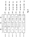
- Specifically, of instructions as disclosed in the above Manual, there are, as shown in Fig. 1, a one-byte LOAD (STORE)
instruction 410, a two-byte LOAD (STORE)instruction 420, a four-byte LOAD (STORE)instruction 430, and an eight-byte LOAD (STORE)instruction 410. Each of theseinstructions operation field 11 composed of 6 bits (Bit Nos. 31-26) and anoperand field 10 composed of 26 bits. Theoperand field 10 consists of afirst field portion 12 composed of 5 bits (Bit Nos. 25-21) indicative of a first register, asecond field portion 13 composed of 5 bits (Bit Nos. 20-16) indicative of a second register, and athird field portion 14 composed of 16 bits (Bit Nos. 15-0) indicative of an immediate data or an offset data. The second field portion 12 (rt) designates a source or destination register, and a memory address is obtained by adding the content of a register designated by the first field portion 12 (base) and the offset value of thethird field portion 14. - The
instructions Instruction Operation Code One-Byte LOAD 100000 Two-Byte LOAD 100001 Four-Byte LOAD 100011 Eight-Byte LOAD 110111 One-Byte STORE 101000 Two-Byte STORE 101001 Four-Byte STORE 101011 Eight-Byte STORE 111111 - In a data transfer performed by the LOAD or STORE instruction, since the memory address is representative of a byte address, when the four-byte LOAD or STORE instruction is, for example, executed, the most least significant two bits of the memory address must be set to "0" in order to transfer four-byte data simultaneously. To this end, the least significant two bits of the
offset field portion 14 are required to written with "0". If at least one of these two bits is written with "1", there occurs trap exception to check a miss-alignment of the memory address. - It is an object of the present invention to provide an improved microprocessor.
- It is another object of the present invention to provide a microprocessor in which the number of instructions to be executed can be increased without expanding the number of bits allotted to an operation field.
- It is still another object of the present invention to provide a microprocessor in which trap exception caused by an address miss-alignment is prevented.
- A microprocessor according to the present invention comprises an execution unit executing a plurality of instructions, each of the instructions having an operation field and an operand field. Of the instructions, there are at least first and second instructions which have the same content of the operation field as each other. The executing unit discriminates a data processing operation required by the first instruction in response only to the content of the operation field thereof and discriminates a data processing operation required by the second instruction in response to the content of the operation field and a part of the content of the operand field thereof.
- It is preferable that the part of the content of the operand field of the second instruction is maked to be "0" irrespective of the actual data thereof. Accordingly, there takes place no address miss-alignment in case of a LOAD or STORE instruction.
- The above and other objects, features and advantages of the present invention will be apparent from the following description taken in conjunction with the accompanying drawings, in which:
- Fig. 1 is an instruction format diagram representative of LOAD or STORE instructions according to the prior art;
- Fig. 2 is a block diagram illustrative of a microprocessor according to an embodiment of the present invention;
- Fig. 3 is an instruction format diagram representative of LOAD or STORE instructions executed by the microprocessor shown in Fig. 2;
- Fig. 4 is a circuit diagram illustrative of a mask circuit shown in Fig. 2; and
- Fig. 5 is an instruction format diagram representative of LOAD and STORE instructions according to another embodiment of the present invention.
- Referring now to Fig. 2, a
microprocessor 500 according to an embodiment of the present invention includes aninstruction register 501 into which an instruction to be executed is temporarily stored from a memory (not shown). Thismicroprocessor 500 is constructed to support or execute various instructions similarly to the prior art microprocessor; however, the instructions as LOAD and STORE instructions executed by themicroprocessor 500 are different in code format from those by the prior art. - Specifically, as is apparent from the comparison between Fig. 1 and Fig. 3, the operation codes among a two-byte LOAD (STORE)
instruction 120, a four-byte LOAD (STORE)instruction 130 and an eight-byte LOAD (STORE)instruction 140 are the same as one another as denoted by "Op-Code II". This operation code Op-Code II is in turn different from the operation code Op-code I of a one-by LOAD (STORE)instruction 110. The detailed codes are as follows:LOAD Instruction STORE Instruction Op-code I 100000 101000 Op-code II 100001 101001 - Since the operation codes are in common to the two-byte, four-byte and eight-byte LOAD (STORE)
instructions offset field portion 14 of anoperand field 10 is made different from one another. Specifically, in the two-byte LOAD (STORE)instruction 120, the least significant bit (LSB) B0 thereof is determined to take "0", as shown in Fig. 3. Similarly, the least significant two bits B1 and B0 of the four-byte LOAD (STORE) instruction are determined to take "0" and "1", respectively, and the least significant three bits B2, B1 and B0 of the eight-byte LOAD (STORE) instruction are determined to take "0", "1" and "1", respectively. - Turning to Fig. 2, of the instruction stored in the
instruction register 501, the operation field 11 (Bit Nos. 31-26) is supplied to adecoder 502, and the field portion 12 (Bit Nos. 25-21) the second field portion 13 (Bit Nos. 20-16) and a part of the offset field portion 14 (Bit Nos. 15-3) except the least significant three bits B2, B1 and B0 are supplied to anaddress calculation unit 506. The least significant three bits B2, B1 and B0 are supplied to amask circuit 504 and aselector 505 and further to thedecoder 502. - The
decoder 502 responds to the operation code produces acontrol signal 5021 which takes a high level when the instruction stored in theregister 501 is one of the two-byte, four-byte and eight-byte LOAD and STORE instructions and a low level when the instruction other than the above instructions is decoded. When one of the two-byte, four-byte and eight-byte LOAD and STORE instructions is decoded, the decoder further refers to the least significant three bits B2 - B0 of the instruction to discriminate which one of those instructions is currently being decoded. In other cases, thedecoder 502 only refers to the operand field. Thus, thedecoder 502 produces decodedoperation code information 5022 which is in turn supplied to an execution unit (EXU) 503 to command a required data processing operation. - The
selector 505 responds to the low level of thecontrol signal 5021 and allows the bits B2 - B0 of theoffset field portion 14 to pass therethrough to theunit 506. When thecontrol signal 5021 takes the high level, on the other hand, theselector 505 selects the output of themask circuit 504 and transfers it to theunit 506. - Referring to Fig. 4, the
mask circuit 504 is composed of aninverter 5041 and aNOR gate 5042 which are connected as shown. Accordingly, themask circuit 504 responds to the data of the bits B2, B1 and B0 and produces mask data consisting of M2, M1 and M0 as shown below.B2 B1 B0 M2 M1 M0 0 0 0 0 0 0 0 0 1 0 0 0 0 1 0 0 1 0 0 1 1 0 0 0 1 0 0 1 0 0 1 0 1 1 0 0 1 1 0 1 1 0 1 1 1 undefined - Thus, when the two-byte LOAD or STORE instruction is decoded, the
address calculation unit 504 always receives the offset value data whose least significant bit is "0". Similarly, theunit 506 always receives the offset value whose least significant two bits are all "0" with respect to the four-byte LOAD or STORE instruction, and receives the offset value data whose least significant three bits are all "0" with respect to the eight-byte LOAD or STORE instruction. Consequently, themicroprocessor 500 does not require such a unit that detects and initiates trap exception for an address miss-alignment. - Moreover, in the
microprocessor 500, there are not required individual operation codes for the two-byte, four-byte and eight-byte LOAD or STORE instructions. Instructions more than those of the prior art are thus supported or executed by themicroprocessor 501. - Referring to Fig. 5, there are shown formats of six instructions 201-206 according to another embodiment of the present invention. Each of the instructions 201-206 is 16-length and includes a register field 130 (Bit Nos. 15-11) indicative of a source or destination register, an operation field 110 (Bit Nos. 10-7) indicative of an operation code, and an offset field 140 (Bit Nos. 6-0) indicative of offset data from a base address for a memory address. The content of the source or destination register is employed as the base address.
- As is apparent from Fig. 5, the operation code of the four-
byte LOAD instruction 205 is the same as that of the four-byte STORE instruction 206, and for this reason, the least significant bit (LSB) B0 of theinstruction 205 is determined to be set with "0", whereas the LSB B0 of theinstruction 206 is determined to be set with "1". - In the instruction formats shown in Fig. 3 or Fig. 5, the positions of the respective fields may be changed. Further, the operation codes of the instructions may be modified.
- It is apparent that the present invention is not limited to the above embodiments but may be modified and changed without departing from the scope of spirit of the invention.
Claims (5)
- A microprocessor comprising execution means for receiving and executing each of a string of instructions, said string of instructions containing first and second instructions, each of said string of instructions including an operation field and an operand field, said execution means discriminating a data processing operation required by said first instruction in response only to said operation field of said first instruction and discriminating a data processing operation required by said second instruction in response to said operation field of said second instruction and a part of said operand field of said second instruction.
- The microprocessor as claimed in claim 1, wherein each of said first and second instructions commands said execution means to perform transfer data between a register and a memory, said execution means performing said data transfer by a first number of bytes in response to said first instruction and by a second number of bytes in response to said second instruction, said first number being different from said second number.
- The microprocessor as claimed in claim 2, wherein said operand field of each of said first and second instructions includes an offset field portion indicative of offset data used for designating an address of said memory, said part of said operand field being contained in said offset field portion.
- A microprocessor comprising storage means for temporarily storing an instruction to be executed, said instruction including an operation field and an operand field, a decoder coupled to said storage means to receive said operation field and a part of said operand field of said instruction, said decoder operating in a first mode to produce decoded information in response to said operation field and in a second mode to produce decoded information in response to said operation field and said part of said operand field, and an execution unit coupled to receive the decoded information from said decoder and executing said instruction in response thereto.
- The microprocessor as claimed in claim 4, further comprising a control circuit to receiving said part of said operand field and operating in said first mode to output said part of said operand field and in said second mode to output predetermined data, and an address calculation unit responding to a remaining part of said operand field and output data of said control circuit and producing an access address.
Applications Claiming Priority (2)
| Application Number | Priority Date | Filing Date | Title |
|---|---|---|---|
| JP6250148A JP2682469B2 (en) | 1994-09-20 | 1994-09-20 | Instruction code encoding method |
| JP250148/94 | 1994-09-20 |
Publications (2)
| Publication Number | Publication Date |
|---|---|
| EP0703529A1 true EP0703529A1 (en) | 1996-03-27 |
| EP0703529B1 EP0703529B1 (en) | 1998-06-17 |
Family
ID=17203536
Family Applications (1)
| Application Number | Title | Priority Date | Filing Date |
|---|---|---|---|
| EP95114573A Expired - Lifetime EP0703529B1 (en) | 1994-09-20 | 1995-09-15 | Microprocessor executing instruction having operand field including portion used as part of operation code |
Country Status (5)
| Country | Link |
|---|---|
| US (1) | US5922067A (en) |
| EP (1) | EP0703529B1 (en) |
| JP (1) | JP2682469B2 (en) |
| KR (1) | KR100229056B1 (en) |
| DE (1) | DE69503010T2 (en) |
Cited By (3)
| Publication number | Priority date | Publication date | Assignee | Title |
|---|---|---|---|---|
| WO1998057256A1 (en) * | 1997-06-10 | 1998-12-17 | Arm Limited | Coprocessor data access control |
| DE102004013176B4 (en) * | 2004-03-17 | 2007-09-06 | Atmel Germany Gmbh | Method and device for executing a program |
| US9619225B2 (en) | 2010-11-23 | 2017-04-11 | Arm Limited | Apparatus and method including an instruction for performing a logical operation on a repeating data value generated based on data size and control parameter portions specified by the instruction |
Families Citing this family (8)
| Publication number | Priority date | Publication date | Assignee | Title |
|---|---|---|---|---|
| DE19629130A1 (en) * | 1996-07-19 | 1998-05-14 | Philips Patentverwaltung | Signal processor |
| KR100308211B1 (en) | 1999-03-27 | 2001-10-29 | 윤종용 | Micro computer system with compressed instruction |
| GB2411976B (en) * | 2003-12-09 | 2006-07-19 | Advanced Risc Mach Ltd | A data processing apparatus and method for moving data between registers and memory |
| US7664933B2 (en) * | 2005-01-17 | 2010-02-16 | Denso Corporation | Microcomputer and encoding system for instruction code and CPU |
| KR100817920B1 (en) * | 2005-12-23 | 2008-03-31 | 엠텍비젼 주식회사 | Embedded system, vertex processing device and decoder |
| JP5263497B2 (en) * | 2008-07-09 | 2013-08-14 | セイコーエプソン株式会社 | Signal processor and semiconductor device |
| JP5263498B2 (en) * | 2008-07-09 | 2013-08-14 | セイコーエプソン株式会社 | Signal processor and semiconductor device |
| US9910674B2 (en) | 2011-04-21 | 2018-03-06 | Renesas Electronics Corporation | Data processor with extended instruction code space including a prohibition combination pattern as a separate instruction |
Citations (4)
| Publication number | Priority date | Publication date | Assignee | Title |
|---|---|---|---|---|
| JPS59148948A (en) * | 1983-02-15 | 1984-08-25 | Nec Corp | Microcomputer |
| EP0306920A2 (en) * | 1987-09-07 | 1989-03-15 | Nec Corporation | Data processor having expanded operating functions |
| EP0535820A2 (en) * | 1991-09-27 | 1993-04-07 | Sun Microsystems, Inc. | Method and apparatus for a register providing atomic access to set and clear individual bits of shared registers without software interlock |
| EP0540175A2 (en) * | 1991-10-29 | 1993-05-05 | Advanced Micro Devices, Inc. | Digital signal processing apparatus |
Family Cites Families (7)
| Publication number | Priority date | Publication date | Assignee | Title |
|---|---|---|---|---|
| CH614100A5 (en) * | 1975-11-10 | 1979-11-15 | Paul Bruggert | |
| FR2407520B1 (en) * | 1977-10-25 | 1989-05-12 | Digital Equipment Corp | CENTRAL PROCESSING UNIT FOR EXECUTING INSTRUCTIONS WITH A SPECIAL OPERAND SPECIFIER |
| US4219874A (en) * | 1978-03-17 | 1980-08-26 | Gusev Valery | Data processing device for variable length multibyte data fields |
| US4236206A (en) * | 1978-10-25 | 1980-11-25 | Digital Equipment Corporation | Central processor unit for executing instructions of variable length |
| US4586131A (en) * | 1982-02-22 | 1986-04-29 | Texas Instruments Incorporated | Microcomputer having data move circuits for within-memory shift of data words |
| US4942552A (en) * | 1986-11-20 | 1990-07-17 | Allen-Bradley Company, Inc. | Method and apparatus for saving and performing industrial control commands |
| JP3547740B2 (en) * | 1992-03-25 | 2004-07-28 | ザイログ,インコーポレイテッド | High-speed instruction decoding pipeline processor |
-
1994
- 1994-09-20 JP JP6250148A patent/JP2682469B2/en not_active Expired - Fee Related
-
1995
- 1995-09-15 DE DE69503010T patent/DE69503010T2/en not_active Expired - Lifetime
- 1995-09-15 EP EP95114573A patent/EP0703529B1/en not_active Expired - Lifetime
- 1995-09-18 US US08/529,606 patent/US5922067A/en not_active Expired - Lifetime
- 1995-09-20 KR KR1019950031739A patent/KR100229056B1/en not_active IP Right Cessation
Patent Citations (4)
| Publication number | Priority date | Publication date | Assignee | Title |
|---|---|---|---|---|
| JPS59148948A (en) * | 1983-02-15 | 1984-08-25 | Nec Corp | Microcomputer |
| EP0306920A2 (en) * | 1987-09-07 | 1989-03-15 | Nec Corporation | Data processor having expanded operating functions |
| EP0535820A2 (en) * | 1991-09-27 | 1993-04-07 | Sun Microsystems, Inc. | Method and apparatus for a register providing atomic access to set and clear individual bits of shared registers without software interlock |
| EP0540175A2 (en) * | 1991-10-29 | 1993-05-05 | Advanced Micro Devices, Inc. | Digital signal processing apparatus |
Non-Patent Citations (3)
| Title |
|---|
| G. L. BAKER, J. B. KIRBY: "Instruction Execution Conditioned on Operand Addresses", IBM TECHNICAL DISCLOSURE BULLETIN, vol. 24, no. 8, NEW YORK US, pages 4018 - 4022 * |
| MIPS R4000 MICROPROCESSOR USER'S MANUAL, 1991, pages A-1 - A-9 |
| PATENT ABSTRACTS OF JAPAN vol. 008, no. 286 (P - 324) 27 December 1984 (1984-12-27) * |
Cited By (7)
| Publication number | Priority date | Publication date | Assignee | Title |
|---|---|---|---|---|
| WO1998057256A1 (en) * | 1997-06-10 | 1998-12-17 | Arm Limited | Coprocessor data access control |
| US6002881A (en) * | 1997-06-10 | 1999-12-14 | Arm Limited | Coprocessor data access control |
| DE102004013176B4 (en) * | 2004-03-17 | 2007-09-06 | Atmel Germany Gmbh | Method and device for executing a program |
| US9063890B2 (en) | 2004-03-17 | 2015-06-23 | Atmel Corporation | Executing program to protected memory in transponder using wireless base station |
| US9619225B2 (en) | 2010-11-23 | 2017-04-11 | Arm Limited | Apparatus and method including an instruction for performing a logical operation on a repeating data value generated based on data size and control parameter portions specified by the instruction |
| US20170153891A1 (en) * | 2010-11-23 | 2017-06-01 | Arm Limited | Data processing apparatus and method |
| US10521232B2 (en) | 2010-11-23 | 2019-12-31 | Arm Limited | Data processing apparatus and method for processing a SIMD instruction specifying a control value having a first portion identifying a selected data size and a second portion identifying at least one control parameter having a number of bits that varies in dependence on a number of bits comprised by the first portion |
Also Published As
| Publication number | Publication date |
|---|---|
| KR100229056B1 (en) | 1999-11-01 |
| US5922067A (en) | 1999-07-13 |
| DE69503010T2 (en) | 1999-02-18 |
| JP2682469B2 (en) | 1997-11-26 |
| EP0703529B1 (en) | 1998-06-17 |
| DE69503010D1 (en) | 1998-07-23 |
| JPH0895780A (en) | 1996-04-12 |
| KR960011683A (en) | 1996-04-20 |
Similar Documents
| Publication | Publication Date | Title |
|---|---|---|
| US5954435A (en) | Memory apparatus and data processor using the same | |
| US6651160B1 (en) | Register set extension for compressed instruction set | |
| EP0220684B1 (en) | Data processing system | |
| EP0169565A2 (en) | Microprocessor compatible with any software represented by different types of instruction formats | |
| JP3203401B2 (en) | Data processing device | |
| JPH06332792A (en) | Data processor, data reading control circuit thereof and data writing control circuit | |
| EP0248436A2 (en) | Method of and apparatus for processing data | |
| EP0703529A1 (en) | Microprocessor executing instruction having operand field including portion used as part of operation code | |
| US7865699B2 (en) | Method and apparatus to extend the number of instruction bits in processors with fixed length instructions, in a manner compatible with existing code | |
| EP0306920B1 (en) | Data processor having expanded operating functions | |
| US4649476A (en) | Microcomputer having an internal address mapper | |
| EP0030463B1 (en) | Buffer memory control system | |
| US5077659A (en) | Data processor employing the same microprograms for data having different bit lengths | |
| US6721867B2 (en) | Memory processing in a microprocessor | |
| US5390358A (en) | Arithmetic unit that requires only one byte instructions | |
| JP2002523836A (en) | Method and apparatus for providing a universal stack | |
| JP2000112754A (en) | Data processor | |
| JPH08185360A (en) | Device for inhibiting read of built-in rom | |
| JPH1040165A (en) | Data read method and read buffer | |
| JPS59106047A (en) | Microcomputer | |
| JPH0226252B2 (en) | ||
| JPH077353B2 (en) | Address selection method | |
| JPS61157945A (en) | Micro instruction read circuit | |
| JPH05334074A (en) | Microprocessor | |
| JPH04315225A (en) | Microcomputer |
Legal Events
| Date | Code | Title | Description |
|---|---|---|---|
| PUAI | Public reference made under article 153(3) epc to a published international application that has entered the european phase |
Free format text: ORIGINAL CODE: 0009012 |
|
| AK | Designated contracting states |
Kind code of ref document: A1 Designated state(s): DE FR GB |
|
| 17P | Request for examination filed |
Effective date: 19960927 |
|
| 17Q | First examination report despatched |
Effective date: 19961122 |
|
| GRAG | Despatch of communication of intention to grant |
Free format text: ORIGINAL CODE: EPIDOS AGRA |
|
| GRAG | Despatch of communication of intention to grant |
Free format text: ORIGINAL CODE: EPIDOS AGRA |
|
| GRAH | Despatch of communication of intention to grant a patent |
Free format text: ORIGINAL CODE: EPIDOS IGRA |
|
| GRAH | Despatch of communication of intention to grant a patent |
Free format text: ORIGINAL CODE: EPIDOS IGRA |
|
| GRAH | Despatch of communication of intention to grant a patent |
Free format text: ORIGINAL CODE: EPIDOS IGRA |
|
| GRAA | (expected) grant |
Free format text: ORIGINAL CODE: 0009210 |
|
| AK | Designated contracting states |
Kind code of ref document: B1 Designated state(s): DE FR GB |
|
| REF | Corresponds to: |
Ref document number: 69503010 Country of ref document: DE Date of ref document: 19980723 |
|
| ET | Fr: translation filed | ||
| PLBE | No opposition filed within time limit |
Free format text: ORIGINAL CODE: 0009261 |
|
| STAA | Information on the status of an ep patent application or granted ep patent |
Free format text: STATUS: NO OPPOSITION FILED WITHIN TIME LIMIT |
|
| 26N | No opposition filed | ||
| REG | Reference to a national code |
Ref country code: GB Ref legal event code: IF02 |
|
| REG | Reference to a national code |
Ref country code: GB Ref legal event code: 732E |
|
| REG | Reference to a national code |
Ref country code: FR Ref legal event code: TP |
|
| REG | Reference to a national code |
Ref country code: FR Ref legal event code: CD |
|
| PGFP | Annual fee paid to national office [announced via postgrant information from national office to epo] |
Ref country code: DE Payment date: 20110907 Year of fee payment: 17 Ref country code: FR Payment date: 20110922 Year of fee payment: 17 Ref country code: GB Payment date: 20110914 Year of fee payment: 17 |
|
| REG | Reference to a national code |
Ref country code: DE Ref legal event code: R082 Ref document number: 69503010 Country of ref document: DE Representative=s name: SPLANEMANN BARONETZKY KNITTER PATENTANWAELTE R, DE |
|
| REG | Reference to a national code |
Ref country code: DE Ref legal event code: R082 Ref document number: 69503010 Country of ref document: DE Representative=s name: SPLANEMANN BARONETZKY KNITTER PATENTANWAELTE R, DE Effective date: 20120828 Ref country code: DE Ref legal event code: R081 Ref document number: 69503010 Country of ref document: DE Owner name: RENESAS ELECTRONICS CORPORATION, JP Free format text: FORMER OWNER: NEC ELECTRONICS CORP., KAWASAKI, JP Effective date: 20120828 |
|
| GBPC | Gb: european patent ceased through non-payment of renewal fee |
Effective date: 20120915 |
|
| REG | Reference to a national code |
Ref country code: FR Ref legal event code: ST Effective date: 20130531 |
|
| PG25 | Lapsed in a contracting state [announced via postgrant information from national office to epo] |
Ref country code: DE Free format text: LAPSE BECAUSE OF NON-PAYMENT OF DUE FEES Effective date: 20130403 Ref country code: GB Free format text: LAPSE BECAUSE OF NON-PAYMENT OF DUE FEES Effective date: 20120915 |
|
| PG25 | Lapsed in a contracting state [announced via postgrant information from national office to epo] |
Ref country code: FR Free format text: LAPSE BECAUSE OF NON-PAYMENT OF DUE FEES Effective date: 20121001 |
|
| REG | Reference to a national code |
Ref country code: DE Ref legal event code: R119 Ref document number: 69503010 Country of ref document: DE Effective date: 20130403 |