EP0342674B1 - Pipeline circuit for timing adjustment - Google Patents
Pipeline circuit for timing adjustment Download PDFInfo
- Publication number
- EP0342674B1 EP0342674B1 EP89108962A EP89108962A EP0342674B1 EP 0342674 B1 EP0342674 B1 EP 0342674B1 EP 89108962 A EP89108962 A EP 89108962A EP 89108962 A EP89108962 A EP 89108962A EP 0342674 B1 EP0342674 B1 EP 0342674B1
- Authority
- EP
- European Patent Office
- Prior art keywords
- data
- input
- signal
- timing
- selection signal
- Prior art date
- Legal status (The legal status is an assumption and is not a legal conclusion. Google has not performed a legal analysis and makes no representation as to the accuracy of the status listed.)
- Expired - Lifetime
Links
Images


Classifications
-
- G—PHYSICS
- G06—COMPUTING; CALCULATING OR COUNTING
- G06F—ELECTRIC DIGITAL DATA PROCESSING
- G06F15/00—Digital computers in general; Data processing equipment in general
- G06F15/76—Architectures of general purpose stored program computers
- G06F15/80—Architectures of general purpose stored program computers comprising an array of processing units with common control, e.g. single instruction multiple data processors
- G06F15/8053—Vector processors
Definitions
- the present invention relates to a pipeline circuit for adjusting the data timing in a data processing system.
- a timing-adjusting pipeline circuit is used for adjusting the timing of data transfers between processing units, particularly for adjusting the timing of data transfers to an interleave type processing unit from another processing unit.
- An interleave type processing unit in this context typically is a memory unit consisting of a plurality of banks which are used in a time-share manner.
- Another example of interleave type processing unit is an arithmetic system comprising a plurality of low-speed arithmetic units which are used in a time-share manner to let the whole system achieve high-speed arithmetic operation.
- a conceivable method of timing adjustment is to adjust the actuating timing of a data processing instruction so that the processed data reach the input crossbar at the interleave timing referred to above.
- This method necessitates no particular timing adjuster.
- it entails complex control of the instruction actuating timing, thereby affects the processing start times of other processing units than the memory and may deteriorate the overall performance of the data processing system.
- a timing-adjusting circuit should be provided immediately before the input crossbar.
- the output timing of the first datum a 1 is adjusted with a selection signal S and those of the succeeding data a 2 , a 3 ,... as inputs to the interleave type processing unit are so controlled as to be identical with the interleave timing by maintaining the selection signal S at the time of the outputting of the datum a 1 .
- this circuit cannot be used when, for instance, the input timings of different data are irregular as is the case with the output data of a processing unit whose processing time differs with the value of each datum or when the series of data include invalid ones that cannot be processed with an interleave type processing unit, such as data for masked vector processing.
- WO-86/03608 discloses a queue administration system which performs validity checks on stored requests for execution.
- An object of the present invention is, therefore, to provide a pipeline circuit for timing adjustment designed to be able to send out at proper timings such data as are effective for ensuing processings even if the input timings of different data are irregular or the input data include invalid ones. This object is solved with the features of the claims.
- the selection signal generating circuit for generating selection signals to determine the durations of data holding by the data holding circuit is controlled with input indicating signals T 1 , T 2 . ..., T j , T m indicating the validity or invalidity of the input data A 1 , A 2 . ..., A j , ..., A m . If the input indicating signals T 1 , T 2 . ..., T j , ..., T m consecutively indicate validity, the selection signal will retain its value for the first input datum, but if an input indicating signal T j indicating invalidity is inputted midway, the selection signal will change to its next value.
- This operation makes it possible, even if the imput timings of different data are irregular or the input data include both valid and invalid ones, to send out at proper timings only effective data for ensuing processings by making ready input indicating signals T 1 , T 2 . ..., T j ,..., T m matching them.
- the data holding circuit even if the input timings of different data are irregular or the input data include both valid and invalid ones, sends out at proper timings only effective data for ensuing processings by controlling the data holding durations and the validity or invalidity of the input data A j in accordance with the selection signals generated by said selection signal generating circuit and said input indicating signals.
- the selection signal generating circuit for generating selection signals to determine the durations of data holding by the data holding circuit is controlled with input indicating signals T 1 , T 2 . ..., T j , ..., T m indicating the validity or invalidity of the input data A 1 , A 2 . ..., A j , ..., A m . If the input indicating signals T 1 , T 2 . ..., T j , ..., T m consecutively indicate validity, the selection signal will retain its value for the first input datum, but if an input indicating signal T j indicating invalidity is inputted midway, the selection signal will change to its next value.
- the output indicating signal V j Indicating whether the input to the n-th data holding means R n of the data holding circuit is to be validated or invalidated is generated by the indicating signal holding circuit on the basis of the input indicating signal T j and the selection signal S j .
- the data holding circuit even if the input timings of different data are irregular or the input data include both valid and invalid ones, sends out at proper timings only effective data for ensuing processings by controlling the data holding durations and the validity or invalidity of the input data A j in accordance with the selection signals generated by the selection signal generating circuit and the output indicating signals generated by the indicating signal holding circuit.
- FIG. 9 is a time chart illustrating the operation of an input crossbar 903 in FIG. 8.
- each of the banks BANK1 to BANK4 of the memory 904 requires two timing cycles of time for the data to be written into.
- An output register ROR1 has a decoder D1 or decoding a selection signal SL1 and a selecting circuit SE1 for selecting and outputting an input corresponding to the output of the decoder D1, and selects and stores the output data from the input register RIA when the reference timing cycle is 1; selects and stores the output data from the input register RIB when the reference timing cycle is 3, and holds the previous data when the reference timing cycle is 2 or 4.
- Output registers ROR2, ROR3 and ROR4 respectively have decoders D2, D3 and D4 for decording selection signals SL2, SL3 and SL4 and selecting circuits SE2, SE3 and SE4 for selecting and outputting their inputs corresponding to the outputs of the decoders D2, D3 and D4, and operate in the same manner as the output register ROR1 in response to the selection signals SL2, SL3 and SL4, respectively.
- the output register ROR1 selects the output datum a 1 from the input register RIA at timing t1 in response to the value "1" of the selection signal SL1, stores it at timing t2 and holds it until timing t3.
- the datum b 1 is stored at timing t4 and is held until timing t5.
- the 4xk+1-th (k is a natural number) data a 1 , b 1 , a 5 , b 5 , a 9 , b 9 , ... of the two serial data A and B are successively stored into the output register ROR1, and become input data for the bank BANK1 of the memory 904.
- the 4 x k+2-th data a 2 , b 2 , a 6 , b 6 , a 10 , b 10 , ... of the two serial data A and B are successively stored into the bank BANK2 through the output register ROR2;
- the 4 x k+3-th data a 3 , b 3 , a 7 , b 7 , a 11 , b 11 , ... of the two serial data A and B are successively stored into the bank BANK3
- the 4 x k+4-th data a 4 , b 4 , a 8 , b 8 , a 12 , b 12 , ... of the two serial data A and B are successively stored into the bank BANK4.
- the 4 x k + 3-th data a 3 , a 7 , a 11 , ... of the serial data A and the 4 x k + 1-th data b 1 , b 5 , b 9 , ... of the serial data B are entered into the input registers RIA and RIB, respectively, when the reference timing cycle is "3"
- the 4 x k + 4-th data a 4 , a 8 , a 12 , ... or the serial data A and the 4 x k + 2-th data b 2 , b 6 , b 10 , ... of the serial data B are entered into the input registers RIA and RIB, respectively, when the reference timing cycle is "4".
- One of the types of data to which the invention applies is a series x of data x 1 , x 2 , ..., x m , wherein the intervals between the elemental data x 1 , x 2 , ... are irregular.
- An example of this type is output data from a processing unit whose processing time differs with the value of each datum or the like.
- Data R (r 1 , r 2 , ..., r m ) outputted from an arithmetic unit or a processor in which arithmetic operations, differing with a datum-corresponding control signal
- V (v 1 , v 2 , ...
- Outputs of such an arithmetic unit require signals indicating the timings of valid data for ensuring data correspondence.
- Validity being represented by "1" and invalidity, by "0"
- all other elemental data g 2 , g 3 , g 4 , g 5 , g 7 , g 8 , ... are invalid data whose values are irrelevant here.
- Another example of irregular intervals between elemental data of a data series is found in data read out of a memory whose access time varies with the address. Further, if data from a processing system whose data transfer rate varies with the mode of use or the state of hardware (for instance, where three processing units are normallv used and two of them continue processing in the event of one running into trouble, the number of processing units at work at a given point of time) are to be placed under the same control irrespective of the mode of use or the state of hardware, there will be required, as described above, the combination of a data series including both valid and invalid data and, corresponding to these data, a signal indicating the validity or invalidity of each elemental datum, and the data and the indicating signal can be represented like the aforementioned data G and indicating signal F, respectively.
- the validity or invalidity of individual data is indicated by another set of data.
- the concept of mask bit is used to distinguish between valid and invalid elemental data among vector data.
- a mask bit indicates valid data among operand vector data, so that valid data alone can be put to arithmetic operation or the operation is executed for all data and the validity or invalidity of the data resulting from the operation is indicated with a mask bit.
- T (1, 0, ..., 1) indicating the validity or invalidity of the data.
- a selection signal S from a selection signal generating circuit 101 is inputted to a data holding circuit 102, and is decoded by a decoder DCD to generate selections signals S 1 , S 2 , S 3 and S 4 for four stages of data holding means R1, R2, R3 and R4, respectively, into one or another of which is stored the input data A. If the selection signal S 3 out of the selection signals S 1 , S 2 , S 3 and S 4 is valid (logical "1"), the data A will be stored into the data holding means R3. The data A stored in the data holding means R3 are stored into the data holding means R4 one timing cycle later, and supplied as the output data of the data holding circuit 102, i.e. the output data Y of the pipeline circuit 1000.
- the data holding means R2 can be realized, for instance as illustrated, with a register RG2 having a two-input one-output selecting circuit SE12 to whose first and second stage inputs are respectively supplied the output of the first data holding means R1 and the input data A and a gate G12 which provides the inverted signal of the selection signal S 2 to the first stage of the selecting circuit SE12 and at the same time the uninverted selection signal S 2 to the second stage of the selecting circuit SE12.
- This data holding means R2 selects and stores the data A when the selection signal S 2 is valid or the output data of the data holding means R1 when the selection signal S 2 is invalid (logical "0").
- the data holding means R3 and R4 can be respectively realized with registers RG3 and RG4 having two-input one-output selecting circuits SE13 and SE14 to whose first and second stage inputs are supplied the outputs of the preceding-stage data holding means R2 and R3 and the input data A, respectively, and gates G13 and G14 which provide the inverted signals of the selection signals S 3 and S 4 to the first stages of the selecting circuits SE13 and SE14 and at the same time the uninverted selection signals S 3 and S 4 to the second stages of the selecting circuits SE13 and SE14.
- the data holding means R1 can be realized with a register RG1 having a selecting circuit SE11 which outputs the data A when the selection signal S 1 is valid and stores the data A through this selecting circuit SE11.
- the selection signal generating circuit 101 referred to above, as illustrated, can be realized with a cycle counter CNT having a two-input one-output selecting circuit SE21 to whose first and second stage inputs are respectively supplied the output of a +1 circuit AD and the current value of the selection signal S and a gate G21 which provides the inverted signal of the input indicating signal T to the first stage of the selecting circuit SE21 and at the same time the uninverted selection signal T to the second stage of same.
- This cycle counter CNT varies the value of the selection signal in synchronism with the timing cycle by selecting the value "S+1", which is the output of the +1 circuit AD, when the input indicating signal T is "0" or the value "S" when T is "1".
- This selection signal S can indicate one of four values, 1, 2, 3 and 4.
- registers RG1 to RG4 in the data holding means R1, R2, R3 and R4 are represented by first, second, third and fourth registers, respectively, and a register which receives the inputting of and stores the output data Y of the pipeline circuit 1000 and outputs them as data Z is represented by a Z register 103.
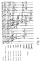
- input indicating signals T corresponding to the input data series A (a 1 , a 2 , a 3 , ...) are supposed to be (0, 1, 0, 0, 1, 1, 0, 0, 0, 1, 0, 0, 0, 0 and 0, ).
- a 2 , a 5 , a 6 , a 10 , and a 13 , ... are valid data and, conversely, a 1 , a 3 , a 4 , a 7 , a 8 , a 9 , a 11 , a 12 , a 14 , a 15 , a 16 , a 17 , and a 18 , ... are invalid data.
- the timing at which the first elemental datum a 1 of the input data series A is entered is supposed to be t1, and the selection signal S at that time, to indicate "2".
- the selection signal S Before the datum a 1 is entered, i.e. before timing t1, the selection signal S periodically varies to indicate one or another of four recurring values, 1, 2, 3, 4, 1, 2, 3, 4 and 1, ... until it indicates "2" at timing t1.
- the datum a 1 stored into the second register RG2 is not stored into the third register RG3 at timing t3 and instead is invalidated.
- the pipeline circuit 1000 is used as pipeline circuits 901 and 902 in FIG. 8, said Z register 103 will correspond to the input registers RIA and RIB.
- FIG. 3 an example of the operation of the pipeline circuit 902 when a reference timing cycle "1" of the input crossbar 903 is assigned to the input register RIA, another reference timing cycle "3" of same, to the input register RIB, and timing t5 shown in FIG. 2 (the timing at which the data a 2 is stored into the Z register 103, i.e. the input register RIA) coincides with the crossbar reference timing "1" (namely the operation shown in FIG. 2 is that of the pipeline circuit 901).
- each reference timing cycle shown here has hardware items, such as a cycle counter, but it is a virtual timing cycle for designing or verifying a circuit for controlling data transfers, so that nothing more is required than for the timings of different parts within the data processing apparatus to be consistent with one another.
- a selection signal S B varies one timing cycle ahead of the crossbar reference timing.
- the valid datum will be stored into the Z register 103 (i.e. the input register RIB) when the crossbar reference timing is "1". Since the crossbar reference timing of "3" is assigned to the input register RIB whose inputs are the data series B as stated above, the operating timing has to be shifted.
- the pipeline circuit 902 can store the first effective datum into the input register RIB when the crossbar reference timing is "3".
- the pipeline circuit 902 will be standing by at timing t4 in a state one timing cycle behind the crossbar reference timing.
- the pipeline circuit 902 will operate in the same manner as the pipeline circuit described with reference to FIG. 2, and data b 1 , b 3 , b 4 , b 5 , b 7 , ... are stored into the fourth register, which also is an output register of the pipeline circuit 902, at timings t6, t10, t11, t12, t13, ..., respectively, and into the Z register, i.e. the input register RIB, at the respectively next timings t7, t11, t12, t13, t14, ... .
- the data entered into the input registers RIA and RIB by the operations illustrated in FIGS. 2 and 3 are further entered into the banks BANK1, BANK2, BANK3 and BANK4 of the memory 904 by the operation shown in the time chart of FIG. 4.
- a reference timing cycle of "1" is assigned to the input register RIA, and one of "3" to the input register RIB.
- the output register ROR1 selects and enters an output datum of the input register RIA when the reference timing cycle is "1"; stores it when the cycle is "2"; selects and enters an output datum of the input register RIB while holding the preceding datum when the cycle is "3”; stores it when the cycle is "4"; selects and enters another output datum of the input register RIA while holding the preceding datum when the cycle is again “1”; stores it when the cycle is again "2", Hence, and repeats these same operations in the four timing cycles.
- the output register ROR2 operates in the same manner as the output register ROR1 except that the former is one timing cycle behind the latter. Thus, it repeats in four timing cycles the operations of selecting and entering an output datum of the input register RIA, storing it at the next timing when the reference timing cycle is "2", selecting and entering an output datum of the input register RIB, and storing it at the next timing when the reference timing cycle is "4".
- the output register ROR3 operates in the same manner as the output register ROR2 except that the former is another timing cycle behind the latter, and this correspondingly applies to the output register ROR4.
- the pipeline circuit according to the present invention is effective for adjusting the timing to supply data, even if the input data include invalid data, to an interleave type processing apparatus in a sequence for valid data alone.
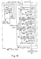
- FIG. 5 is a block diagram of a second preferred embodiment of the present invention, where the advantage of the pipeline circuit according to the invention is increased by having not only the input data series A but also the input indicating signals T, as referred to in the first embodiment shown in FIG. 1, inputted to a data holding circuit 502.
- the data holding circuit 502 receives a selection signal S from a selection signal generating circuit 501, decodes it with a decoder DCD into selection signals S 1 , S 2 , S 3 and S 4 for four stages of data holding means R1, R2, R3 and R4, respectively, and stores data P, each of which consists of a pair of one of the data A and an input indicating signal T corresponding to that datum, into one of the four-stage data holding means R1, R2, R3 and R4. If, for instance, the selection signal S 3 out of the selection signals S 1 , S 2 , S 3 and S 4 is valid, the data P will be stored into the data holding means R3.
- the data P stored in the data holding means R3 are stored into the data holding means R4 one timing cycle later to become the output data of the data holding circuit 502, i.e. of the pipeline circuit 5000.
- a register combining said E register and Z register will correspond to the input registers RIA and RIB of the input crossbar 903, but partial registers corresponding to the E register will be referred to as EIA and EIB and those corresponding to the Z register, as RIA and RIB here as illustrated in FIG. 7 for the convenience of description.
- the registers RIA and EIA operate in the same manner, and so do the registers RIB and EIB.
- partial registers EOR1 to EOR4 as shown in FIG.
- registers ROR1 and EOR1 operate in the same manner and so do the pair of registers ROR2 and EOR2, that of registers ROR3 and EOR3 and that of registers ROR4 and EOR4.
- An example of operation in the input crossbar 903 when the pipeline circuit 5000 is used as the pipeline circuits 901 and 902 in FIG. 7 will be described below with reference to the block diagram of FIG. 7 and the time chart of FIG. 6.
- the datum a 2 and the indicating signal "1" for it stored into the output registers ROR1 and EOR1 at timing t6 are entered into the bank BANK1 of the memory and, as the indicating signal is "1", the datum a 2 is stored into the bank BANK1 of the memory at timing t7.
- the datum a 4 and the indicating signal "0" for it stored into the output registers ROR2 and EOR2 at timing t7 are entered into the bank BANK2 of the memory, but, as the indicating signal is "0", the datum a 4 is not stored therein.
- the data a 2 , b 3 , ... are stored into the bank BANK1, the data a 5 , b 4 , ..., into the bank BANK2, the data a 6 , b 5 , ..., into the bank BANK3, and the data a 10 , b 7 , ..., into the bank BANK4 of the memory.
- pipeline circuit 5000 of FIG. 5 represents an addition, to the functions of the pipeline circuit 1000 of FIG. 1, of another function to convey the indication of validity or invalidity of the output data to another circuit downstream.
- a data holding circuit 302 receives the inputting of a selection signal S from a selection signal generating circuit 101, generates selection signals S 1 , S 2 , S 3 and S 4 for four stages of data holding means R1', R2', R3' and R4', respectively, by decoding the selection signal S, and stores the input data A into one of the four-stage data holding means R1', R2', R3' and R4'. If, for instance, the selection signal S 3 out of the selection signals S 1 , S 2 , S 3 and S 4 is valid (logical "1" for example), the data A will be stored into the data holding means R3'.
- the data A will be invalidated and not stored into the data holding means R3′.
- the data A, stored into the data holding means R3′ when the input indicating signal T is valid, are stored into the data holding means R4′ one timing cycle later, and supplied as the output data of the data holding circuit 302, i.e. as the output data Y of the pipeline circuit 3000.
- the data holding means R2′ can be realized with a register RG2 having a two-input one-output selecting circuit SE12 to whose first and second-stage inputs are supplied the output of the first data holding means R1′ and the input data A, respectively, a gate G12 which provides the inverted signal of the selection signal S 2 to the first stage of the selecting circuit SE12 and at the same time outputs the uninverted selection signal S 2 and a gate G16 which supplies the logical product of the input indicating signal T and the selection signal S 2 to the second stage of the selecting circuit SE12. It selects and stores the data A when both the input indicating signal T and the selection signal S 2 are valid or the output data of the data holding means R1′ when the selecting signal S 2 is invalid.
- the data holding means R3′ and R4′ can be respectively realized with registers RG3 and RG4 having two-input one-output selecting circuits SE13 and SE14 to whose first and second stage inputs are supplied the outputs of the preceding-stage data holding means R2′ and R3′ and the input data A, respectively, and gates G15 and G17 which provide the inverted signals of the selection signals S 3 and S 4 to the first stages of the selecting circuits SE13 and SE14 and at the same time the uninverted selection signals S 3 and S 4 to the second stages of the selecting circuits SE13 and SE14.
- the data holding means R1′ can be realized with a register RG1 having a selecting circuit SE11 which outputs the data A when the output of a gate G11 supplying the logical product of the selection signal S 1 and the input indicating signal T is valid, and stores the data A through this selecting circuit SE11.
- the selection signal generating circuit 101 referred to above can be realized, as illustrated, with a cycle counter CNT having a two-input one-output selecting circuit SE21 to whose first and second stage inputs are respectively supplied the output of a +1 circuit AD and the current value of the selection signal S and a gate G21 which provides the inverted signal of the input indicating signal T to the first stage of the selecting circuit SE21 and at the same time the uninverted selection signal T to the second stage of same.
- This cycle counter CNT varies the value of the selection signal in synchronism with the timing cycle by selecting the value "S+1", which is the output of the +1 circuit AD, when the input indicating signal T is "0" or the value "S" when the input indicating signal T is "1".
- This selection signal S can indicate one of four values, 1, 2, 3 and 4.
- registers RG1 to RG4 in the data holding means R1′, R2′, R3′ and R4′ are representec by first, second, third and fourth registers, respectively, and a register which receives the inputting of and stores the output data Y of the pipeline circuit 3000 and outputs them as data Z is represented by a Z register 103.
- input indicating signals T corresponding to the input serial data A (a 1 , a 2 , a 3 , ...) are supposed to be (0, 1, 0, 0, 1, 1, 0, 0, 0, 1, 0, 0, 0 and 0, ).
- a 2 , a 5 , a 6 , a 10 , and a 13 , ... are valid data and, conversely, a 1 , a 3 , a 4 , a 7 , a 8 , a 9 , a 11 , a 12 , a 14 , a 15 , a 16 , and a 17 , ... are invalid data.
- the timing at which the first elemental datum a 1 of the input data series A is entered is supposed to be t1, and the selection signal S at that time, to indicate "2".
- the selection signal S Before the datum a 1 is entered, i.e. before timing t1, the selection signal S periodically varies to indicate one or another of four recurring values, 1, 2, 3, 4, 1, 2, 3, 4 and 1, ... until it indicates "2" at timing t1.
- the datum a 1 inputted at timing t1 is not entered into the second register RG2 and is invalidated instead, though the selection signal S is "2" at that time, because the input indicating signal is invalid (logical "0").
- the datum a 3 entered at timing t3 is not entered into the third register RG3 at timing t3 and instead is invalidated, though the selection signal S at that time indicates "3", because the input indicating signal T indicates "0".
- the datum a 4 entered at timing t4 is not entered into the fourth register RG4 and is invalidated instead because the selection signal S and input indicating signal T at that time are "4" and "0", respectively.
- Similar operations are repeated at and after timing t5, and into the fourth register RG4, which also is the output register of the pipeline circuit 3000, are stored the data a 2 , a 5 , a 6 , a 10 , a 13 , ... at timings t4, t9, t10, t11, t16 ..., respectively, each to become an element datum of the output data series Y of the pipeline circuit 3000, and stored into the Z register 103 at the respectively next timings t5, t10, t11, t12, t17 ...
- a selection signal S B varies one timing cycle ahead of the crossbar reference timing.
- the valid datum will be stored into the Z register 103 (i.e. the input register RIB) when the crossbar reference timing is "1". Since the crossbar reference timing of "3" is assigned to the input register RIB whose inputs are the data series B as stated above, the operating timing has to be shifted.
- the pipeline circuit 902 can store the first valid datum into the input register RIB when the crossbar reference timing is "3".
- the pipeline circuit 902 will be standing by at timing t4 in a state one timing cycle behind the crossbar reference timing.
- the pipeline circuit 902 will operate in the same manner as the pipeline circuit described with reference to FIG. 2, and data b 3 , b 4 , b 5 , b 7 , b 8 , ... are stored into the fourth register, which also is an output register of the pipeline circuit 902, at timings t10, t11, t12, t13, t14 ..., respectively, and into the Z register, i.e. the input register RIB, at the respectively next timings t11, t12, t13, t14, t15, ...
- the data entered into the input registers RIA and RIB by the operations illustrated in FIGS. 11 and 12 are further entered into the banks BANK1, BANK2, BANK3 and BAND4 of the memory 904 by the operation shown in the time chart of FIG. 4.
- a reference timing cycle of "1" is assigned to the input register RIA, and one of "3" to the input register RIB.
- the output register ROR1 selects and enters an output datum of the input register RIA when the reference timing cycle is "1"; stores it when the cycle is "2"; selects and enters an output datum of the input register RIB while holding the preceding datum when the cycle is "3”; stores it when the cycle is "4"; selects and enters another output datum of the input register RIA while holding the preceding datum when the cycle is again “1”; stores it when the cycle is again "2", Hence, and repeats these same operations in the four timing cycles.
- the output register ROR2 operates in the same manner as the output register ROR1 except that the former is one timing cycle behind the latter. Thus, it repeats in four timing cycles the operations of selecting and entering an output datum of the input register RIA, storing it at the next timing when the reference timing cycle is "2", selecting and entering an output datum of the input register RIB, and storing it at the next timing when the reference timing cycle is "4".
- the output register ROR3 operates in the same manner as the output register ROR2 except that the former is another timing cycle behind the latter, and this correspondingly applies to the output register ROR4.
- the datum a 2 stored into the input register RIA at timing t5 is stored into the output register ROR1 at timing t6 when the reference timing cycle is "1”
- the datum a 5 stored into the input register RIA at timing t10 is stored into the output register ROR2 at timing t11 when the reference timing cycle is "2”
- the data a 2 and b 3 stored into the input registers RIA and RIB at timing t11 are stored into the output registers ROR3 and ROR1, respectively, at timing t12 when the reference timing cycle is "3".
- Similar operations are repeated thereafter, and the data a 2 , b 3 , b 8 , a 13 ...
- the pipeline circuit according to the present invention is effective for adjusting the timing to supply data, even if the input data include invalid data, to an interleave type processing apparatus in a sequence for valid data alone.
- FIG. 14 is a block diagram of a fourth preferred embodiment of the present invention, where the advantage of the pipeline circuit according to the invention is increased by having not only the input serial data A but also the input indicating signals T, as referred to in the third embodiment shown in FIG. 10, inputted to a data holding circuit.
- the same reference numerals as in FIG. 10 denote respectively the same constituent elements.
- the data holding circuit 602 receives the inputting of a selection signal S from a selection signal generating circuit 101, decoders it with a decoder DCD into selection signals S 1 , S 2 , S 3 and S 4 for four stages of data holding means R1 ⁇ , R2 ⁇ , R3 ⁇ and R4 ⁇ , respectively, and stores data P, each of which consists of a pair of one of the data A and an input indicating signal T corresponding to that datum, into one of the four-stage data holding means R1 ⁇ , R2 ⁇ , R3 ⁇ and R4 ⁇ .
- the data P will be stored into the data holding means R3 ⁇ , though the data P will be invalidated and not stored into the data holding means R3 ⁇ if the input indicating signal indicates invalidity (logical "0" for instance).
- the data P stored in the data holding means R3 ⁇ when the input indicating signal T indicates validity (logical "1" for instance) are stored into the data holding means R4 ⁇ one timing cycle later to become the output data of the data holding circuit 602, i.e. of the pipeline circuit 6000.
- a Z register 603 and an E register 604 for respectively storing output data Y, which correspond to the input data A of the output data of the data holding circuit 602, and data H corresponding to the input indicating signals T of same, and outputting them as data Z and E.
- the data H can be used as control signals for the data Y (for instance as write enable signals or the like) in another circuit downstream.
- FIG. 15 is a block diagram of a fifth preferred embodiment of the present invention, where the advantage of the pipeline circuit according to the invention is increased by inputting not only the input serial data A and the input indicating signals T, as referred to in the third embodiment shown in FIG. 10, but also a selection signal initial value S0 and an initial value setting indicating signal ST.
- Equivalent constituent elements to those in FIG. 10 are denoted by respectively the same reference numerals.
- a selection signal generating circuit 303 having the selection signal initial value S0, the initial value setting indicating signal ST and the input indicating signal T as inputs, outputs the selection signal initial value S0 as the selection signal S of the next timing when the initial value setting indicating signal ST indicates validity; generates and outputs the selection signal indicating the value next to what was indicated by the preceding selection signal S out of the four periodic values 1, 2, 3, 4, 1, 2, ... when both the initial value setting indicating signal ST and the input indicating signal T indicate invalidity; and holds the value indicated by the preceding selection signal S when the initial value setting indicating signal ST and the input indicating signal T respectively indicate invalidity and validity.
- the selection signal generating circuit 303 referred to above, as illustrated, can be realized with a cycle counter CNT2 having a three-input one-output selecting circuit SE31 to whose first, second and third stage input are respectively supplied the selection signal initial value S0, the output of a +1 circuit AD and the current value of the selection signal S; a gate G31 which provides the initial value setting indicating signal ST to the first stage of the selecting circuit SE31 and at the same time generates its inverted signal; a gate G32 which outputs the input indicating signal T and its inverted signal; a gate G33 which provides the logical product of the inverted signal of the initial value setting indicating signal ST and that of the input indicating signal T to the second stage of the selecting circuit SE31; and a gate G34 which provides the logical product of the inverted signal of the initial value setting indicating signal ST and the input indicating signal T to the third stage of the selecting circuit SE31.
- This cycle counter CNT2 varies the value of the selection signal in synchronism with the timing cycle by selecting the value of the selection signal initial value S0 when the initial value setting indicating signal ST indicates “1", the value "S+1" when both the initial value setting indicating signal ST and the input indicating signal T indicate “0", or the value "S” when the initial value setting indicating signal ST indicates “0" and the input indicating signal T indicates "1".
- This selection signal S can indicate one of four values, 1, 2, 3 and 4.
- the pipeline circuit 7000 described above if used, for instance, as the pipeline circuit 902 described with reference to FIGS. 12 and 8, can adjust the timing of the selecting signal S, so that the first valid datum can be stored into the input register RIB when the crossbar reference timing is "3", by inputting a value one timing cycle behind the crossbar reference timing as the selection signal initial value S0 together with the initial value setting indicating signal ST.
- the data holding circuit 202 receives the inputting of a selection signal S from a selection signal generating circuit 101, decodes it with a decoder DCD1 into selection signals S 1 , S 2 , S 3 and S 4 for four stages of data holding means R1, R2, R3 and R4 ⁇ , respectively, and stores input data A into one of the four-stage data holding means R1, R2, R3 and R4 ⁇ . If, for instance, the selection signal S 3 out of the selection signals S 1 , S 2 , S 3 and S 4 is valid (logical "1" for instance), the data A will be stored into the data holding means R3.
- the selection signal S 4 is invalidated when the output indicating signal from an indicating signal holding circuit 203 is invalid (logical "0" for example), the data A will not be stored into the data holding means R4 ⁇ and invalidated instead.
- the data A stored in the data holding means R3 are stored into the data holding means R4 one timing cycle later to be supplied as the output data of the data holding circuit 202, i.e. the output data Y of the pipeline circuit 2000. If, however, the output indicating signal V one timing cycle later than the timing at which the data A were stored into the data holding means R3 indicates invalidity, the output data of the data holding means R3 will not be stored into the data holding means R4 and be invalidated instead.
- the data holding means R2 can be realized with a register RG2 having a two-input one-output selecting circuit SE12 to whose first and second stage inputs are respectively supplied the output of the data holding means R1 and the input data A, and a gate G12 which provides the inverted signal of the selection signal S 2 to the first stage of the selecting circuit SE12 and at the same time the uninverted selection signal S 2 to the second stage of the selecting circuit SE12. It selects and stores the data A when the selecting signal S 2 is valid or the output data of the data holding means R1 when the selection signal S 2 is invalid (logical "0").
- the data holding means R3 like the data holding means R2, can be realized with registers RG3 having two-input one-output selecting circuits SE13 to whose first and second stage inputs are supplied the outputs of the preceding-stage data holding means R2 and the input data A, respectively, and a gate G13 which provides the inverted signal of the selection signal S 3 to the first stage of the selecting circuit SE13 and at the same time the uninverted selection signal S 3 to the second stage of the selecting circuit SE13.
- the data holding means R1 can be realized with a register RG1 having a selecting circuit SE11 which outputs the data A when the selection signal S 1 is valid and stores the data A through this selecting circuit SE11.
- the data holding means R4 can be realized with a register RG4 having a two-input one-output selecting circuit SE14 to whose first and second stage inputs are respectively supplied the output of the preceding-stage data holding means R3 and the input data A; a gate G14 which supplies the selection signal S 4 and its inverted output; a gate G19 which obtains the logical product of the output indicating signal V and the inverted output of said selection signal and supplies the output to the first stage of the selecting circuit SE14, and a gate G18 which obtains the logical product of the selection signal S 4 and the output indicating signal V and supplies the output to the second stage of the selecting circuit SE14.
- the output of the gate G18 is validated, and the second stage of the selecting circuit SE14 is selected, so that the data A are stored into the register RG4; when the selecting signal S 4 is invalid (logical "0") and the output indicating signal V is valid, the output of the gate G19 is validated and the first stage of the selecting circuit SE14 is selected, so that the output data of the data holding means R3 are stored into the register RG4; or when the output indicating signal V is invalid, nothing is stored and the input data are invalidated (all the bits are "0" for instance).
- the selection signal generating circuit 101 referred to above, as illustrated, can be realized with a cycle counter CNT1 having a two-input one-output selecting circuit SE21 to whose first and second stage inputs are respectively supplied the output of a +1 circuit AD and the current value of the selection signal S, and a gate G21 which provides the inverted signal of the input indicating signal T to the first stage of the selecting circuit SE21 and at the same time the uninverted input indicating signal to the second stage of the selecting circuit SE21.
- This cycle counter CNT1 varies the value of the selection signal in synchronism with the timing cycle by selecting the value "S+1", which is the output of the +1 circuit AD, when the input indicating signal T indicates "0", or the value "S" when the input indicating signal indicates "1".
- This selection signal S can indicate one of four values, 1, 2, 3 and 4.
- the indicating signal holding circuit 203 receives the inputting of the selection signal S, from which it generates with a decoder DCD2 selection signals S 1 , S 2 and S 3 for three stages of indicating signal holding means F1, F2 and F3, respectively, and a selection signal S 4 for a selecting circuit SE34 for supplying the output indicating signal V, and decides whether to store the input indicating signal T into one of the three-stage indicating signal holding means F1, F2 and F3 or to supply it as the output indicating signal V. If the selection signal S 3 , for instance, out of the selection signals S 1 , S 2 , S 3 and S 4 is valid, the input indicating signal T is stored into the indicating signal holding means F3.
- the input indicating signal T stored into the indicating signal holding means F3 is supplied one timing cycle later from the selecting circuit SE34 as the output indicating signal V. If the selection signal S 4 out of the selection signals S 1 , S 2 , S 3 and S 4 is valid, the input indicating signal T will be directly supplied as the output indicating signal V from the selecting circuit SE34.
- the indicating signal holding means F2 can be realized with a register RG12 having a two-input one-output selecting circuit SE32 to whose first and second stage inputs are respectively supplied the output of the preceding-stage indicating signal holding means F1 and the input indicating signal T, and a gate G31 which provides the inverted signal of the selection signal S 2 to the first stage of the selecting circuit SE32 and at the same time the uninverted selection signal S 2 to the second stage of the selecting circuit SE32. It selects and stores the input indicating signal T when the selection signal S 2 is valid (logical "1") or the output data of the indicating signal holding means F1 when the selection signal S 2 is invalid (logical "0").
- the indicating signal holding means F3 can be realized with a register RG13 having a two-input one-output selecting circuit SE33 to whose first and second-stage inputs are supplied the output of the preceding-stage indicating signal holding means F2 and the input indicating signal T, respectively, and a gate G32 which provides the inverted signal of the selection signal S 3 to the first stage of the selecting circuit SE33 and at the same time the uninverted selection signal S 3 to the second stage of same.
- the indicating signal holding means F1 can be realized with a register RG11 having a selecting circuit SE31 which outputs the input indicating signal T when the selection signal S 1 is valid and stores the input indicating signal T through this selecting circuit SE31.
- a gate G33 supplies the inverted signal of the selection signal S 4 to the first stage of a selecting circuit SE34 and at the same time the uninverted selection signal S 4 to the second stage of same.
- the selecting circuit SE34 supplies the output of the indicating signal holding means F3 as the output indicating signal V when the first stage is selected by the gate G33 or the input indicating signal T as the output indicating signal V when the second stage is selected.
- registers RG1 to RG4 in the data holding means R1, R2, R3 and R4 are represented by first, second, third and fourth registers, respectively, and a register which receives the inputting of and stores the output data Y of the pipeline circuit 2000 and outputs them as data Z is represented by a Z register 10B.
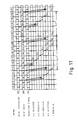
- input indicating signals T corresponding to the input data series A (a 1 , a 2 , a 3 , ...) are supposed to be (0, 1, 0, 0, 1, 1, 0, 0, 0, 1, 0, 0, 0 and 0, ).
- a 2 , a 5 , a 6 , a 10 , and a 13 , ... are valid data and, conversely, a 1 , a 3 , a 4 , a 7 , a 8 , a 9 , a 11 , a 12 , a 14 , a 15 , a 16 and a 17 , ... are invalid data.
- the timing at which the first elemental datum a 1 of the input data series A is entered is supposed to be t1, and the selection signal S at that time, to indicate "2".
- the selection signal S Before the datum a 1 is entered, i.e. before timing t1, the selection signal S periodically varies to indicate one or another of four recurring values, 1, 2, 3, 4, 1, 2, 3, 4 and 1, ... until it indicates "2" at timing t1.
- the datum a 1 inputted at timing t1 is entered into the second register RG2 and stored at the next timing t2.
- the datum a 1 stored into the second register RG2 at timing t 2 is not stored into the third register RG3 and instead invalidated at timing t3.
- the datum a 4 entered at timing t4 is not entered into the fourth register RG4 and is invalidated instead because the selection signal S and input indicating signal T at that time are "4" and "0", respectively.
- Similar operations are repeated at and after timing t5, and into the fourth register RG4, which also is the output register of the pipeline circuit 2000, are stored the data a 2 , a 5 , a 6 , a 10 , a 13 , ... at timings t4, t9, t10, t11, t16 ..., respectively, each to become an element datum of the output data series Y of the pipeline circuit 2000, and stored into the Z register 103 at the respectively next timings t5, t10, t11, t12, t17 ...
- a selection signal S B varies one timing cycle ahead of the crossbar reference timing.
- the valid datum will be stored into the Z register 103 (i.e. the input register RIB) when the crossbar reference timing is "1". Since the crossbar reference timing of "3" is assigned to the input register RIB whose inputs are the data series B as stated above, the operating timing has to be shifted.
- the pipeline circuit 902 can store the first valid datum into the input register RIB when the crossbar reference timing is "3".
- the pipeline circuit 902 will be standing by at timing t4 in a state one timing cycle behind the crossbar reference timing.
- the pipeline circuit 902 will operate in the same manner as the pipeline circuit described with reference to FIG. 17, and data b 3 , b 4 , b 5 , b 7 and b 8 , ... will be stored into the fourth register, which also is an output register of the pipeline circuit 902, at timings t10, t11, t12, t13 and t14 ..., respectively, and into the Z register, i.e. the input register RIB, at the respectively next timings t11, t12, t13, t14 and t15, ...
- the data entered into the input registers RIA and RIB by the operations illustrated in FIGS. 17 and 18 are further entered into the banks BANK1, BANK2, BANK3 and BANK4 of the memory 904 by the operation shown in the time chart of FIG. 19.
- a reference timing cycle of "1" is assigned to the input register RIA, and one of "3" to the input register RIB.
- the output register ROR1 selects and enters an output datum of the input register RIA when the reference timing cycle is "1"; stores it when the cycle is "2"; selects and enters an output datum of the input register RIB while holding the preceding datum when the cycle is "3”; stores it when the cycle is "4"; selects and enters another output datum of the input register RIA while holding the preceding datum when the cycle is again “1”; stores it when the cycle is again "2", Hence, and repeats these same operations in the four timing cycles.
- the output register ROR2 operates in the same manner as the output register ROR1 except that the former is one timing cycle behind the latter. Thus, it repeats in four timing cycles the operations of selecting and entering an output datum of the input register RIA, storing it at the next timing when the reference timing cycle is "2", selecting and entering an output datum of the input register RIB, and storing it at the next timing when the reference timing cycle is "4".
- the output register ROR3 operates in the same manner as the output register ROR2 except that the former is another timing cycle behind the latter, and this correspondingly applies to the output register ROR4.
- the datum a 2 stored into the input register RIA at timing t5 is stored into the output register ROR1 at timing t6 when the reference timing cycle is "1”
- the datum a 5 stored into the input register RIA at timing t10 is stored into the output register ROR2 at timing t11 when the reference timing cycle is "2”
- the data a 6 and b 3 stored into the input registers RIA and RIB at timing tll are stored into the output registers ROR3 and ROR1, respectively, at timing t12 when the reference timing cycle is "3".
- Similar operations are repeated thereafter, and the data a 2 , b 3 , b 8 , a 13 , ...
- the pipeline circuit according to the present invention is effective for adjusting the timing to supply data, even if the input data include invalid data, to an interleave type processing apparatus in a sequence for valid data alone.
- FIG. 20 is a block diagram of a seventh preferred embodiment of the present invention, where the advantage of the pipeline circuit according to the invention is increased by supplying the output indicating signal H besides the output data Y, as referred to in -he sixth embodiment shown in FIG. 16.
- the same reference numerals as in FIG. 16 denote respectively the same constituent elements.
- an indicating signal holding circuit 205 receives the inputting of the selection signal S from a selection signal generating circuit 101, generates from it, with a decoder DCD2, selection signals S 1 , S 2 , S 3 , and S 4 for four stages of indicating signal holding means F1, F2, F3 and F4, respectively, and stores the input indicating signal T into one of the four-stage indicating signal holding means F1, F2, F3 and F4. If the selection signal S 3 , for instance, out of the selection signals S 1 , S 2 , S 3 and S 4 is valid, the input indicating signal T is stored into the indicating signal holding means F3. The input indicating signal T stored into the indicating signal holding means F3 is supplied one timing cycle later as the output indicating signal V, at the same time entered into the indicating signal holding means F4, and stored and outputted another timing cycle later.
- the input indicating signal T will be directly supplied as the output indicating signal V from a selecting circuit SE34, entered into the indicating signal holding means F4, and stored and outputted one timing cycle later.
- the output of the indicating signal holding means F4 is supplied as the output data H of the pipeline circuit 4000 stored into an E register 207 and, together with the output Z of a Z register 103, handed over to a succeeding circuit. Since the data Y outputted from the data holding circuit 202 at a timing at which the output data H are valid (logical "1" for example) are always valid, the data H, i.e. the output E of the E register 207, can be used as a control signal (for instance a write enable signal or the like) for the output Z of the Z register 103 in a circuit down-stream.
- a control signal for instance a write enable signal or the like
- FIG. 21 is a block diagram of an eighth preferred embodiment of the present invention, where the advantage of the pipeline circuit according to the invention is increased by inputting not only the input data series A and the input indicating signals T, as referred to in the sixth embodiment shown in FIG. 16, but also a selection signal initial value S0 and an initial value setting indicating signal ST. Equivalent constituent elements to those in FIG. 16 are denoted by respectively the same reference numerals.
- a selection signal generating circuit 208 having the selection signal initial value S0, the initial value setting indicating signal ST and the input indicating signal T as inputs, outputs the selection signal initial value S0 as the selection signal S of the next timing when the initial value setting indicating signal ST indicates validity; generates and outputs the selection signal indicating the value next to what was indicated by the preceding selection signal S out of the four periodic values 1, 2, 3, 4, 1 and 2, ... when both the initial value setting indicating signal ST and the input indicating signal T indicate invalidity; and holds the value indicated by the preceding selection signal S when the initial value setting indicating signal ST and the input indicating signal T respectively indicate invalidity and validity.
- the selection signal generating circuit 208 referred to above, as illustrated, can be realized with a cycle counter CNT2 having a three-input one-output selecting circuit SE41 to whose first, second and third stage inputs are respectively supplied the selection signal initial value S0, the output of a +1 circuit AD and the current value of the selection signal S; a gate G41 which provides the initial value setting indicating signal ST to the first stage of the selecting circuit SE41 and at the same time generates its inverted signal; a gate G42 which outputs the input indicating signal T and its inverted signal; a gate G43 which provides the logical product of the inverted signal of the initial value setting indicating signal ST and that of the input indicating signal T to the second stage of the selecting circuit SE41; and a gate G44 which provides the logical product of the inverted signal of the initial value setting indicating signal ST and the input indicating signal T to the third stage of the selecting circuit SE41.
- This cycle counter CNT2 varies the value of the selection signal in synchronism with the timing cycle by selecting the value of the selection signal initial value S0 when the initial value setting indicating signal ST indicates “1", the value "S+1" when both the initial value setting indicating signal ST and the input indicating signal T indicate “0", or the value "S” when the initial value setting indicating signal ST indicates “0" and the input indicating signal T indicates "1".
- This selection signal S can indicate one of four values, 1, 2, 3 and 4.
- the pipeline circuit 6000 described above can adjust the timing of the selecting signal S, so that the first valid datum can be stored into the input register RIB when the crossbar reference timing is "3", by inputting a value one timing cycle behind the crossbar reference timing as the selection signal initial value S0 together with the initial value setting indicating signal ST.
- the pipeline circuit according to the present invention offers the benefits that, even if data input timings are irregular or the data include both valid and invalid ones, valid data alone can be sent out at appropriate timings by controlling the generation of selection signals for determining the duration of data holding within the pipeline circuit by using a signal indicating the validity or invalidity of input data, and that the circuit for said control can be realized with simple and small hardware.
Description
- The present invention relates to a pipeline circuit for adjusting the data timing in a data processing system.
- Usually, a timing-adjusting pipeline circuit is used for adjusting the timing of data transfers between processing units, particularly for adjusting the timing of data transfers to an interleave type processing unit from another processing unit.
- An interleave type processing unit in this context typically is a memory unit consisting of a plurality of banks which are used in a time-share manner. Another example of interleave type processing unit is an arithmetic system comprising a plurality of low-speed arithmetic units which are used in a time-share manner to let the whole system achieve high-speed arithmetic operation.
- In an actual data processing system, in order that data to be written into a memory match their interleave timing as input data to an interleave type processing unit, some kind of timing adjustment is required.
- A conceivable method of timing adjustment is to adjust the actuating timing of a data processing instruction so that the processed data reach the input crossbar at the interleave timing referred to above. This method necessitates no particular timing adjuster. However, it entails complex control of the instruction actuating timing, thereby affects the processing start times of other processing units than the memory and may deteriorate the overall performance of the data processing system.
- Therefore, a timing-adjusting circuit should be provided immediately before the input crossbar.
- If a series of data A = (a1, a2, ..., am) is inputted, the output timing of the first datum a1 is adjusted with a selection signal S and those of the succeeding data a2, a3,... as inputs to the interleave type processing unit are so controlled as to be identical with the interleave timing by maintaining the selection signal S at the time of the outputting of the datum a1. However, this circuit cannot be used when, for instance, the input timings of different data are irregular as is the case with the output data of a processing unit whose processing time differs with the value of each datum or when the series of data include invalid ones that cannot be processed with an interleave type processing unit, such as data for masked vector processing.
- WO-86/03608 discloses a queue administration system which performs validity checks on stored requests for execution.
- An object of the present invention is, therefore, to provide a pipeline circuit for timing adjustment designed to be able to send out at proper timings such data as are effective for ensuing processings even if the input timings of different data are irregular or the input data include invalid ones. This object is solved with the features of the claims.
- According to a first embodiment the selection signal generating circuit for generating selection signals to determine the durations of data holding by the data holding circuit is controlled with input indicating signals T1, T2. ..., Tj, Tm indicating the validity or invalidity of the input data A1, A2. ..., Aj, ..., Am. If the input indicating signals T1, T2. ..., Tj, ..., Tm consecutively indicate validity, the selection signal will retain its value for the first input datum, but if an input indicating signal Tj indicating invalidity is inputted midway, the selection signal will change to its next value. This operation makes it possible, even if the imput timings of different data are irregular or the input data include both valid and invalid ones, to send out at proper timings only effective data for ensuing processings by making ready input indicating signals T1, T2. ..., Tj,..., Tm matching them.
- The data holding circuit, even if the input timings of different data are irregular or the input data include both valid and invalid ones, sends out at proper timings only effective data for ensuing processings by controlling the data holding durations and the validity or invalidity of the input data Aj in accordance with the selection signals generated by said selection signal generating circuit and said input indicating signals.
- According to a second embodiment the selection signal generating circuit for generating selection signals to determine the durations of data holding by the data holding circuit is controlled with input indicating signals T1, T2. ..., Tj, ..., Tm indicating the validity or invalidity of the input data A1, A2. ..., Aj, ..., Am. If the input indicating signals T1, T2. ..., Tj, ..., Tm consecutively indicate validity, the selection signal will retain its value for the first input datum, but if an input indicating signal Tj indicating invalidity is inputted midway, the selection signal will change to its next value. Further, the output indicating signal Vj Indicating whether the input to the n-th data holding means Rn of the data holding circuit is to be validated or invalidated is generated by the indicating signal holding circuit on the basis of the input indicating signal Tj and the selection signal Sj. The data holding circuit, even if the input timings of different data are irregular or the input data include both valid and invalid ones, sends out at proper timings only effective data for ensuing processings by controlling the data holding durations and the validity or invalidity of the input data Aj in accordance with the selection signals generated by the selection signal generating circuit and the output indicating signals generated by the indicating signal holding circuit.
- Features and advantages of the present invention will become more apparent from the following detailed description when taken in conjunction with the accompanying drawings, in which:
- FIG. 1 is a block diagram of a first preferred embodiment of the invention;
- FIG. 2 is a time chart illustrating the operation within the pipeline circuit which is the first preferred embodiment of the invention;
- FIG. 3 is a time chart illustrating one example of a method to stagger the operating timings of the pipeline circuit illustrated in FIG. 1;
- FIG. 4 is a timing chart illustrating an example of the operation of an input crossbar using an output from the pipeline circuit which is the first preferred embodiment of the invention;
- FIG. 5 is a block diagram of a second preferred embodiment of the invention;
- FIG. 6 is a timing chart illustrating an example of the operation of an input crossbar using an output from the pipeline circuit which is the second embodiment of the invention;
- FIG. 7 is a block diagram of an example of the configuration of memory-peripheral circuits to which the pipeline circuit, which is the second embodiment, is applied;
- FIG. 8 is a block diagram of an example of the configuration of a data processing apparatus having a memory comprising four banks;
- FIG. 9 is a time chart illustrating an example of the operation of the
input crossbar 903 of FIG. 8; - FIG. 10 is a block diagram of a third preferred embodiment of the invention;
- FIG. 11 is a time chart illustrating the operation within the pipeline circuit which is the third preferred embodiment of the invention;
- FIG. 12 is a time chart illustrating one example of method to stagger the operating timings of the pipeline circuit illustrated in FIG. 10;
- FIG. 13 is a timing chart illustrating an example of the operation of an input crossbar using an output from the pipeline circuit which is the third preferred embodiment of the invention;
- FIG. 14 is a block diagram of a fourth preferred embodiment of the invention;
- FIG. 15 is a block diagram of a fifth preferred embodiment of the invention;
- FIG. 16 is a block diagram of a sixth preferred embodiment of the invention;
- FIG. 17 is a time chart illustrating the operation within the pipeline circuit which is the sixth preferred embodiment of the invention;
- FIG. 18 is a time chart illustrating one example of a method to stagger the operating timings of the pipeline circuit illustrated in FIG. 16;
- FIG. 19 is a timing chart illustrating an example of the operation of an input crossbar using an output from the pipeline circuit which is the sixth preferred embodiment of the invention;
- FIG. 20 is a block diagram of a seventh preferred embodiment of the invention; and
- FIG. 21 is a block diagram of a eighth preferred embodiment of the invention.
- In the figures, the same reference numerals denote respectively the same constituent elements.
- FIG. 8 is a typical block diagram of memory-peripheral circuits of a data processing apparatus capable of writing a series of data A = (a1, a2, ..., am) and another series of data B = (b1, b2, ..., bm) into a
memory 904 comprising four banks, BANK1, BANK2, BANK3 and BANK4. FIG. 9 is a time chart illustrating the operation of aninput crossbar 903 in FIG. 8. - Referring to FIGS. 8 and 9, each of the banks BANK1 to BANK4 of the
memory 904 requires two timing cycles of time for the data to be written into. An input register RIA, whose input is the series of data A = (a1, a2, ..., am), is assigned areference timing cycle 1 of the crossbar control an another input register RIB, whose input is the series of data B = (b1, b2, ..., bm) , is assigned areference timing cycle 3 of same. - An output register ROR1 has a decoder D1 or decoding a selection signal SL1 and a selecting circuit SE1 for selecting and outputting an input corresponding to the output of the decoder D1, and selects and stores the output data from the input register RIA when the reference timing cycle is 1; selects and stores the output data from the input register RIB when the reference timing cycle is 3, and holds the previous data when the reference timing cycle is 2 or 4.
- Output registers ROR2, ROR3 and ROR4 respectively have decoders D2, D3 and D4 for decording selection signals SL2, SL3 and SL4 and selecting circuits SE2, SE3 and SE4 for selecting and outputting their inputs corresponding to the outputs of the decoders D2, D3 and D4, and operate in the same manner as the output register ROR1 in response to the selection signals SL2, SL3 and SL4, respectively.
- Referring now to FIG. 9, the output register ROR1 selects the output datum a1 from the input register RIA at timing t1 in response to the value "1" of the selection signal SL1, stores it at timing t2 and holds it until timing t3. As it selects the output datum b1 from the input register RIB in response to the value "3" of the selection signal SL1, the datum b1 is stored at timing t4 and is held until timing t5. In this manner, the 4xk+1-th (k is a natural number) data a1, b1, a5, b5, a9, b9, ... of the two serial data A and B are successively stored into the output register ROR1, and become input data for the bank BANK1 of the
memory 904. - Similarly, the 4 x k+2-th data a2, b2, a6, b6, a10, b10, ... of the two serial data A and B are successively stored into the bank BANK2 through the output register ROR2; the 4 x k+3-th data a3, b3, a7, b7, a11, b11, ... of the two serial data A and B are successively stored into the bank BANK3, and the 4 x k+4-th data a4, b4, a8, b8, a12, b12, ... of the two serial data A and B are successively stored into the bank BANK4.
- The operations described with reference to FIG. 9 presupposes that 4 x k + 1-th data a1, a5, a9, ... of the serial data A is entered into the input register RIA and the 4 x k + 3-th data b3, b7, b11, ... of the serial data B are entered into the input register RIB when the reference timing cycle of the
input crossbar 903 is "1", the 4 x k + 2-th data a2, a6, a10, ... of the serial data A and the 4 x k + 4-th data b4, b8, b12, ... of the serial data B are entered into the input registers RIA and RIB, respectively, when the reference timing cycle is "2", the 4 x k + 3-th data a3, a7, a11, ... of the serial data A and the 4 x k + 1-th data b1, b5, b9, ... of the serial data B are entered into the input registers RIA and RIB, respectively, when the reference timing cycle is "3", and the 4 x k + 4-th data a4, a8, a12, ... or the serial data A and the 4 x k + 2-th data b2, b6, b10, ... of the serial data B are entered into the input registers RIA and RIB, respectively, when the reference timing cycle is "4". - Now will be explained a form of data to which the present invention applies and the way in which the form of data is described below.
- One of the types of data to which the invention applies is a series x of data x1, x2, ..., xm, wherein the intervals between the elemental data x1, x2, ... are irregular.
- An example of this type is output data from a processing unit whose processing time differs with the value of each datum or the like. Data R = (r1, r2, ..., rm) outputted from an arithmetic unit or a processor in which arithmetic operations, differing with a datum-corresponding control signal V = (v1, v2, ... vm), take place between a series Y of operand data y1, y2,..., ym and another series W of operand data w1, w2, ..., wm, and the processing time differs with the type of operation, the value of datum and the like, are an example of the irregular intervals between elemental data as mentioned above. Where data are successively outputted at irregular intervals, for instance the second datum r2 appears five timing cycles after the first datum r1 and the third r3 does three timing cycles after that, if the arithmetic unit is a type which holds a datum until the next datum is outputted, a description of equal intervals on the time axis (i.e. at every timing cycle) will be D = (r1, r1, r1, r1, r1, r1, r2, r2, r2, r3, ..., rm), and a case in which invalid data appear between valid data will be represented in such a way as E = (r1, -, -, -, -, r2, -; -, r3, ..., rm). Outputs of such an arithmetic unit require signals indicating the timings of valid data for ensuring data correspondence. Validity being represented by "1" and invalidity, by "0", a signal F indicating a valid datum and the above data D or E will be F = (1, 0, 0, 0, 0, 1, 0, 0, 1, ..., 1), and correspond to data G = (g1, g2, ..., gt) representing D and E. In the foregoing examples, g1 = r1, g6 = r2, g9 = r3 ..., gt = rm, and all other elemental data g2, g3, g4, g5, g7, g8, ... are invalid data whose values are irrelevant here.
- Another example of irregular intervals between elemental data of a data series is found in data read out of a memory whose access time varies with the address. Further, if data from a processing system whose data transfer rate varies with the mode of use or the state of hardware (for instance, where three processing units are normallv used and two of them continue processing in the event of one running into trouble, the number of processing units at work at a given point of time) are to be placed under the same control irrespective of the mode of use or the state of hardware, there will be required, as described above, the combination of a data series including both valid and invalid data and, corresponding to these data, a signal indicating the validity or invalidity of each elemental datum, and the data and the indicating signal can be represented like the aforementioned data G and indicating signal F, respectively.
- In still another type of data to which the present invention applies, the validity or invalidity of individual data is indicated by another set of data. In a vector data processing apparatus, for instance, the concept of mask bit is used to distinguish between valid and invalid elemental data among vector data. A mask bit indicates valid data among operand vector data, so that valid data alone can be put to arithmetic operation or the operation is executed for all data and the validity or invalidity of the data resulting from the operation is indicated with a mask bit. These manners of operation are known as masked operations. Like the data of the first type described above, the vector data can be represented by H = (h1, h2, ..., ht) and the mask data, by J = (j1, j2, ..., jt).
- Now, in the following description, said first and second types will be represented by an input data series A (a1, a2, ..., am) and indicating signals T = (1, 0, ..., 1) indicating the validity or invalidity of the data. This means that, where elemental data a1, a2 ..., am are consecutively inputted in every timing cycle, a1 is a valid datum, a2, an invalid datum, and ..., am are valid data.
- Referring now to FIG. 1, a
pipeline circuit 1000 in the first preferred embodiment of the present invention receives an input indicating signal T and a data series A = (a1, a2, ..., am) as inputs, and outputs a data series Y = (y1, y2 ..., ym). - A selection signal S from a selection
signal generating circuit 101 is inputted to adata holding circuit 102, and is decoded by a decoder DCD to generate selections signals S1, S2, S3 and S4 for four stages of data holding means R1, R2, R3 and R4, respectively, into one or another of which is stored the input data A. If the selection signal S3 out of the selection signals S1, S2, S3 and S4 is valid (logical "1"), the data A will be stored into the data holding means R3. The data A stored in the data holding means R3 are stored into the data holding means R4 one timing cycle later, and supplied as the output data of thedata holding circuit 102, i.e. the output data Y of thepipeline circuit 1000. - The data holding means R2 can be realized, for instance as illustrated, with a register RG2 having a two-input one-output selecting circuit SE12 to whose first and second stage inputs are respectively supplied the output of the first data holding means R1 and the input data A and a gate G12 which provides the inverted signal of the selection signal S2 to the first stage of the selecting circuit SE12 and at the same time the uninverted selection signal S2 to the second stage of the selecting circuit SE12. This data holding means R2 selects and stores the data A when the selection signal S2 is valid or the output data of the data holding means R1 when the selection signal S2 is invalid (logical "0").
- The data holding means R3 and R4, like the data holding means R2, can be respectively realized with registers RG3 and RG4 having two-input one-output selecting circuits SE13 and SE14 to whose first and second stage inputs are supplied the outputs of the preceding-stage data holding means R2 and R3 and the input data A, respectively, and gates G13 and G14 which provide the inverted signals of the selection signals S3 and S4 to the first stages of the selecting circuits SE13 and SE14 and at the same time the uninverted selection signals S3 and S4 to the second stages of the selecting circuits SE13 and SE14. The data holding means R1 can be realized with a register RG1 having a selecting circuit SE11 which outputs the data A when the selection signal S1 is valid and stores the data A through this selecting circuit SE11.
- The selection
signal generating circuit 101, when the input indicating signal T entered corresponding to the data A indicates invalidity (logical "0"), generates and outputs a selection signal S indicating the value next to that indicated by the preceding selection signal S out of fourperiodic values - Conversely, if the input indicating signal T indicates validity (logical "1"), the selection
signal generating circuit 101 will hold the value indicated by the preceding selection signal S. If, for instance, an input indicating signal T = 1 is inputted when the selection signal S indicates "1", the selection signal S will indicate "1" at the next timing, too. - The selection
signal generating circuit 101 referred to above, as illustrated, can be realized with a cycle counter CNT having a two-input one-output selecting circuit SE21 to whose first and second stage inputs are respectively supplied the output of a +1 circuit AD and the current value of the selection signal S and a gate G21 which provides the inverted signal of the input indicating signal T to the first stage of the selecting circuit SE21 and at the same time the uninverted selection signal T to the second stage of same. This cycle counter CNT varies the value of the selection signal in synchronism with the timing cycle by selecting the value "S+1", which is the output of the +1 circuit AD, when the input indicating signal T is "0" or the value "S" when T is "1". This selection signal S can indicate one of four values, 1, 2, 3 and 4. - The operation of the
pipeline circuit 1000 will be described below with reference to the time chart of FIG. 2, in which said registers RG1 to RG4 in the data holding means R1, R2, R3 and R4 are represented by first, second, third and fourth registers, respectively, and a register which receives the inputting of and stores the output data Y of thepipeline circuit 1000 and outputs them as data Z is represented by aZ register 103. - In FIG. 2, input indicating signals T corresponding to the input data series A = (a1, a2, a3, ...) are supposed to be (0, 1, 0, 0, 1, 1, 0, 0, 0, 1, 0, 0, 1, 0, 0, 0, 0 and 0, ...). Thus a2, a5, a6, a10, and a13, ... are valid data and, conversely, a1, a3, a4, a7, a8, a9, a11, a12, a14, a15, a16, a17, and a18, ... are invalid data.
- Further, the timing at which the first elemental datum a1 of the input data series A is entered is supposed to be t1, and the selection signal S at that time, to indicate "2". Before the datum a1 is entered, i.e. before timing t1, the selection signal S periodically varies to indicate one or another of four recurring values, 1, 2, 3, 4, 1, 2, 3, 4 and 1, ... until it indicates "2" at timing t1.
- Referring to FIG. 2, the datum a1 inputted at timing t1 is entered into the second register RG2 in response to the selection signal S (= 2) at that time, and stored at the next timing t2. The selection signal S at timing t2 indicates "3", the value next to that of the selection signal S (= 2) of timing t1 in response to the input indicating signal T (= 0) at the preceding timing t1.
- Then, the datum a2 inputted at timing t2 is entered into the third register RG3 in response to the selection signal S (= 3) at that time, and stored at the next timing t3. The datum a1 stored into the second register RG2 is not stored into the third register RG3 at timing t3 and instead is invalidated. The selection signal S at timing t3, in response to the input indicating signal T (= 1) at the preceding timing t2, is stored at timings t4, t5, t9, t10, t11, t12, t16 and t17, ... to become an element datum of the output data series Y of the
pipeline circuit 1000, and stored into theZ register 103 at the respectively next timings t5, t6, t10, t11, t12, t13, t17 and t18, ... . - The intervals of the output timings of the valid data a2, a5, a6, a10, a13, ... among the elemental data of the input serial data A = (a1, a2, a3, ...) are 4xk+1 timing cycles (k is an integer), such as 5 (= 4 x 1 + 1) timing cycles between the data a2 and a5, 1 (= 4 x 0 + 1) timing cycle between the data a5 and a6, 1 timing cycle between the data a6 and a10, 5 timing cycles between the data a10 and a13, ... .
- If the
pipeline circuit 1000 is used aspipeline circuits pipeline circuit 902 when a reference timing cycle "1" of theinput crossbar 903 is assigned to the input register RIA, another reference timing cycle "3" of same, to the input register RIB, and timing t5 shown in FIG. 2 (the timing at which the data a2 is stored into theZ register 103, i.e. the input register RIA) coincides with the crossbar reference timing "1" (namely the operation shown in FIG. 2 is that of the pipeline circuit 901). - It is not meant that each reference timing cycle shown here has hardware items, such as a cycle counter, but it is a virtual timing cycle for designing or verifying a circuit for controlling data transfers, so that nothing more is required than for the timings of different parts within the data processing apparatus to be consistent with one another.
- Referring now to FIG. 3, at timings before timing t0, a selection signal SB varies one timing cycle ahead of the crossbar reference timing. Thus, if the first valid datum is inputted (accompanied by the input indicating signal T (= 1)) in this state, the valid datum will be stored into the Z register 103 (i.e. the input register RIB) when the crossbar reference timing is "1". Since the crossbar reference timing of "3" is assigned to the input register RIB whose inputs are the data series B as stated above, the operating timing has to be shifted.
- If, for instance, a dummy input indicating signal T = 1 is inputted twice at timings preceding the inputting of the first valid datum, the
pipeline circuit 902 can store the first effective datum into the input register RIB when the crossbar reference timing is "3". Thus, referring to FIG. 3, by inputting the dummy input indicating signal T = 1 at timings t2 and t3, thepipeline circuit 902 will be standing by at timing t4 in a state one timing cycle behind the crossbar reference timing. - If, in that state, the input data series B (= b1, b2, b3, ...) and the input indicating signals T (= 0, 0, 1, 1, 1, 0, 1, 1, 0, 0, 0, 1, ...) corresponding to the data are entered from timing t5 on, the
pipeline circuit 902 will operate in the same manner as the pipeline circuit described with reference to FIG. 2, and data b1, b3, b4, b5, b7, ... are stored into the fourth register, which also is an output register of thepipeline circuit 902, at timings t6, t10, t11, t12, t13, ..., respectively, and into the Z register, i.e. the input register RIB, at the respectively next timings t7, t11, t12, t13, t14, ... . - The data entered into the input registers RIA and RIB by the operations illustrated in FIGS. 2 and 3 are further entered into the banks BANK1, BANK2, BANK3 and BANK4 of the
memory 904 by the operation shown in the time chart of FIG. 4. - As stated above, a reference timing cycle of "1" is assigned to the input register RIA, and one of "3" to the input register RIB. The output register ROR1 selects and enters an output datum of the input register RIA when the reference timing cycle is "1"; stores it when the cycle is "2"; selects and enters an output datum of the input register RIB while holding the preceding datum when the cycle is "3"; stores it when the cycle is "4"; selects and enters another output datum of the input register RIA while holding the preceding datum when the cycle is again "1"; stores it when the cycle is again "2", ......, and repeats these same operations in the four timing cycles. As also described above, the output register ROR2 operates in the same manner as the output register ROR1 except that the former is one timing cycle behind the latter. Thus, it repeats in four timing cycles the operations of selecting and entering an output datum of the input register RIA, storing it at the next timing when the reference timing cycle is "2", selecting and entering an output datum of the input register RIB, and storing it at the next timing when the reference timing cycle is "4". The output register ROR3 operates in the same manner as the output register ROR2 except that the former is another timing cycle behind the latter, and this correspondingly applies to the output register ROR4.
- As a result of these operations, as shown in FIG. 4, when the reference timing cycle is "1", the datum a2 stored into the input register RIA at timing t5 is stored into the output register ROR1 at timing t6, and the datum a4 stored into the input register RIA at timing t6 is stored into the output register ROR2 at timing t7; and when the reference timing cycle is "3", the datum b1 stored into the input register RIB at timing t7 is stored into the output register ROR1 at timing t8. Similar operations are repeated thereafter, and the data a2, b1, b3, a11, b8, a13, ... are entered into the bank BANK1 of the memory via the output register ROR1, the data a4, a5, b4, b10, a16, ... are entered into the bank BANK2 of the memory via the output register ROR2, the data a6, b5, ... are entered into the bank BANK3 of the memory via the output register ROR3, and the data a10, b7, ... are entered into the bank BANK4 of the memory via the output register ROR4.
- To consider here a serial data D (= d1, d2, d3, d4, d5, ... = a2, a5, a6, a10, a13, ...) comprising only valid ones out of the serial data A (= a1, a2, a3, ...) and a serial data F (=f1, f2, f3, f4, f5, ... = b3, b4, b5, b7, b8, ...) only valid ones out of the serial data B (= b1, b2, b3, ...), it is seen that the 4xk+1-th (k is an integer) data d1 (= a2), f1 (=b3), d5 (= a13), f5 (= b8), ... of the serial data D and F are entered into the bank BANK1 of the memory; the 4xk+2-th (k is an integer) data d2 (= a5), f2 (=b4), ... of the data series D and F, into the bank BANK2 of the memory; the 4xk+3-th data d3 (= a6), f3 (= b5), ... of the data series D and F, into the bank BANK3 of the memory; and the 4xk+4-th data d4 (= a10), f4 (= b7), ... of the data series D and F, into the bank BANK4 of the memory.
- Thus it is seen that the pipeline circuit according to the present invention is effective for adjusting the timing to supply data, even if the input data include invalid data, to an interleave type processing apparatus in a sequence for valid data alone.
- FIG. 5 is a block diagram of a second preferred embodiment of the present invention, where the advantage of the pipeline circuit according to the invention is increased by having not only the input data series A but also the input indicating signals T, as referred to in the first embodiment shown in FIG. 1, inputted to a
data holding circuit 502. - Referring to FIG. 5, a
pipeline circuit 5000 has input indicating signals T and a data series A (= a1, a2, ..., am), and supplies output indicating signals H and a data series Y. - The
data holding circuit 502 receives a selection signal S from a selectionsignal generating circuit 501, decodes it with a decoder DCD into selection signals S1, S2, S3 and S4 for four stages of data holding means R1, R2, R3 and R4, respectively, and stores data P, each of which consists of a pair of one of the data A and an input indicating signal T corresponding to that datum, into one of the four-stage data holding means R1, R2, R3 and R4. If, for instance, the selection signal S3 out of the selection signals S1, S2, S3 and S4 is valid, the data P will be stored into the data holding means R3. The data P stored in the data holding means R3 are stored into the data holding means R4 one timing cycle later to become the output data of thedata holding circuit 502, i.e. of thepipeline circuit 5000. There are aZ register 503 and anE register 504 for respectively storing output data Y, which correspond to the input data A of the output data of thedata holding circuit 502, and data H corresponding to the input indicating signals T of same, and outputting them as data Z and E. - Description of other parts of the
pipeline circuit 5000 is dispensed with because they are equivalent to those of thepipeline circuit 1000 of FIG. 1. - If the
pipeline circuit 5000 is used as thepipeline circuits input crossbar 903, but partial registers corresponding to the E register will be referred to as EIA and EIB and those corresponding to the Z register, as RIA and RIB here as illustrated in FIG. 7 for the convenience of description. The registers RIA and EIA operate in the same manner, and so do the registers RIB and EIB. Similarly, partial registers EOR1 to EOR4, as shown in FIG. 7, are also added as output registers, and it is supposed that the registers ROR1 and EOR1 operate in the same manner and so do the pair of registers ROR2 and EOR2, that of registers ROR3 and EOR3 and that of registers ROR4 and EOR4. An example of operation in theinput crossbar 903 when thepipeline circuit 5000 is used as thepipeline circuits - Input indicating signals corresponding to the input serial data A = (a1, a2, a3, ...) to the
pipeline circuit 901 being represented by TA (= 0, 1, 0, 0, 1, 1, 0, 0, 0, 1, 0, 0, 1, 0, 0, 0, 0, ...) and those corresponding to the input serial data B = (b1, b2,b3, ...) to thepipeline circuit 902 being represented by TB (= 0, 0, 1, 1, 1, 0, 1, 1, 0, 0, 0, 1, ...), these data are entered into the input registers RIA, EIA, RIB and EIB of thecrossbar 903 as shown in FIG. 6 in the same manner as in the first embodiment described with reference to FIGS. 1 to 4. - Referring to FIG. 6, when the reference timing cycle is "1", the datum a2 and the indicating signal "1" for the data a2 respectively stored at timing t5 into the input registers RIA and EIA are stored at timing t6 into the output registers ROR1 and EOR1; the datum a4 and the indicating signal "0" for the data a4 respectively stored at timing t6 into the input registers RIA and EIA are stored at timing t7 into the output registers ROR2 and EOR2, and when the reference timing cycle is "3", the datum b1 and the indicating signal "0" for the data b1 respectively stored at timing t7 into the input registers RIA and EIB are stored at timing t8 into the output registers ROR1 and EOR1. Similar operations are repeated thereafter, so that the data a2, b1,b3, a11, ... are stored into the output register ROR1; indicating
signals signals signals signals - The datum a2 and the indicating signal "1" for it stored into the output registers ROR1 and EOR1 at timing t6 are entered into the bank BANK1 of the memory and, as the indicating signal is "1", the datum a2 is stored into the bank BANK1 of the memory at timing t7.
- The datum a4 and the indicating signal "0" for it stored into the output registers ROR2 and EOR2 at timing t7 are entered into the bank BANK2 of the memory, but, as the indicating signal is "0", the datum a4 is not stored therein.
- Thereafter, by similar operations, the data a2, b3, ... are stored into the bank BANK1, the data a5, b4, ..., into the bank BANK2, the data a6, b5, ..., into the bank BANK3, and the data a10, b7, ..., into the bank BANK4 of the memory.
- By the operations described so far, the valid data a2, a5, a6, a10, a13, ... out of the input serial data A (= a1, a2, a3, ...) and the valid data b3, b4, b5, b7, b8, ... out of the input serial data B (= b1, b2, b3, ...) entered into the pipeline circuit are stored in the memory in the sequence of valid data alone.
- Thus the
pipeline circuit 5000 of FIG. 5 represents an addition, to the functions of thepipeline circuit 1000 of FIG. 1, of another function to convey the indication of validity or invalidity of the output data to another circuit downstream. - Referring now to FIG. 10, a
pipeline circuit 3000 in a third preferred embodiment of the present invention has input indication signals T and a serial data A (= a1, a2, ..., am) as its inputs and outputs a serial data Y (y1, y2, ..., yt). - A
data holding circuit 302 receives the inputting of a selection signal S from a selectionsignal generating circuit 101, generates selection signals S1, S2, S3 and S4 for four stages of data holding means R1', R2', R3' and R4', respectively, by decoding the selection signal S, and stores the input data A into one of the four-stage data holding means R1', R2', R3' and R4'. If, for instance, the selection signal S3 out of the selection signals S1, S2, S3 and S4 is valid (logical "1" for example), the data A will be stored into the data holding means R3'. If, however, the input indicating signal is invalid (logical "0" for example), the data A will be invalidated and not stored into the data holding means R3′. The data A, stored into the data holding means R3′ when the input indicating signal T is valid, are stored into the data holding means R4′ one timing cycle later, and supplied as the output data of thedata holding circuit 302, i.e. as the output data Y of thepipeline circuit 3000. - The data holding means R2′, for instance as illustrated, can be realized with a register RG2 having a two-input one-output selecting circuit SE12 to whose first and second-stage inputs are supplied the output of the first data holding means R1′ and the input data A, respectively, a gate G12 which provides the inverted signal of the selection signal S2 to the first stage of the selecting circuit SE12 and at the same time outputs the uninverted selection signal S2 and a gate G16 which supplies the logical product of the input indicating signal T and the selection signal S2 to the second stage of the selecting circuit SE12. It selects and stores the data A when both the input indicating signal T and the selection signal S2 are valid or the output data of the data holding means R1′ when the selecting signal S2 is invalid.
- The data holding means R3′ and R4′, like the data holding means R2′, can be respectively realized with registers RG3 and RG4 having two-input one-output selecting circuits SE13 and SE14 to whose first and second stage inputs are supplied the outputs of the preceding-stage data holding means R2′ and R3′ and the input data A, respectively, and gates G15 and G17 which provide the inverted signals of the selection signals S3 and S4 to the first stages of the selecting circuits SE13 and SE14 and at the same time the uninverted selection signals S3 and S4 to the second stages of the selecting circuits SE13 and SE14. The data holding means R1′ can be realized with a register RG1 having a selecting circuit SE11 which outputs the data A when the output of a gate G11 supplying the logical product of the selection signal S1 and the input indicating signal T is valid, and stores the data A through this selecting circuit SE11.
- The selection
signal generating circuit 101, when the input indicating signal T entered corresponding to the data A indicates invalidity (logical "0"), generates and outputs a selection signal S indicating the value next to that indicated by the preceding selection signal S out of fourperiodic values - Conversely, if the input indicating signal T indicates validity (logical "1"), the selection
signal generating circuit 101 will hold the value indicated by the preceding selection signal S. If, for instance, an input indicating signal T = 0 is inputted when the selection signal S indicates "1", the selection signal S will indicate "1" at the next timing, too. - The selection
signal generating circuit 101 referred to above can be realized, as illustrated, with a cycle counter CNT having a two-input one-output selecting circuit SE21 to whose first and second stage inputs are respectively supplied the output of a +1 circuit AD and the current value of the selection signal S and a gate G21 which provides the inverted signal of the input indicating signal T to the first stage of the selecting circuit SE21 and at the same time the uninverted selection signal T to the second stage of same. This cycle counter CNT varies the value of the selection signal in synchronism with the timing cycle by selecting the value "S+1", which is the output of the +1 circuit AD, when the input indicating signal T is "0" or the value "S" when the input indicating signal T is "1". This selection signal S can indicate one of four values, 1, 2, 3 and 4. - The operation of the
pipeline circuit 3000 will be described below with reference to the time chart of FIG. 11, in which said registers RG1 to RG4 in the data holding means R1′, R2′, R3′ and R4′ are representec by first, second, third and fourth registers, respectively, and a register which receives the inputting of and stores the output data Y of thepipeline circuit 3000 and outputs them as data Z is represented by aZ register 103. - In FIG. 11, input indicating signals T corresponding to the input serial data A = (a1, a2, a3, ...) are supposed to be (0, 1, 0, 0, 1, 1, 0, 0, 0, 1, 0, 0, 1, 0, 0, 0 and 0, ...). Thus a2, a5, a6, a10, and a13, ... are valid data and, conversely, a1, a3, a4, a7, a8, a9, a11, a12, a14, a15, a16, and a17, ... are invalid data.
- Further, the timing at which the first elemental datum a1 of the input data series A is entered is supposed to be t1, and the selection signal S at that time, to indicate "2". Before the datum a1 is entered, i.e. before timing t1, the selection signal S periodically varies to indicate one or another of four recurring values, 1, 2, 3, 4, 1, 2, 3, 4 and 1, ... until it indicates "2" at timing t1.
- Referring to FIG. 11, the datum a1 inputted at timing t1 is not entered into the second register RG2 and is invalidated instead, though the selection signal S is "2" at that time, because the input indicating signal is invalid (logical "0"). The selection signal S at timing t2 indicates "3", the value next to that of the selection signal S (= 2) of timing t1 in response to the input indicating signal T (= 0) at the preceding timing t1.
- Then, the datum a2 inputted at timing t2 is entered into the third register RG3 in response to the selection signal S (= 3) at that time because the input indicating signal T is valid (logical "1"), and stored at the next timing t3. The selection signal S at timing t3 holds the selection signal S (= 3) of timing t2 in response to the input indicating signal T (= 1) at the preceding timing t2.
- In response to the selection signal S (= 3) of timing t3, the output datum a2 of the third register RG3 is entered into the fourth register RG4, and stored at the next timing t4.
- Further, the datum a3 entered at timing t3 is not entered into the third register RG3 at timing t3 and instead is invalidated, though the selection signal S at that time indicates "3", because the input indicating signal T indicates "0". The selection signal S at timing t4, in response to the input indicating signal T (= 0) of timing t3 and the selection signal of "3", indicates the next value "4".
- The datum a4 entered at timing t4 is not entered into the fourth register RG4 and is invalidated instead because the selection signal S and input indicating signal T at that time are "4" and "0", respectively. The selection signal S at timing t5, in response to the input indicating signal T (= 0) and the selection signal of "4" at timing t4, indicates the next value "1".
- Similar operations are repeated at and after timing t5, and into the fourth register RG4, which also is the output register of the
pipeline circuit 3000, are stored the data a2, a5, a6, a10, a13, ... at timings t4, t9, t10, t11, t16 ..., respectively, each to become an element datum of the output data series Y of thepipeline circuit 3000, and stored into theZ register 103 at the respectively next timings t5, t10, t11, t12, t17 ... - Here, the intervals of the output timings of the valid data a2, a5, a6, a10, a13, ... among the elemental data of the input data series A = (a1, a2, a3, ...) are 4xk+1 timing cycles (k is an integer), such as 5 (= 4 x 1 + 1) timing cycles between the data a2 and a5, 1 (= 4 x 0 + 1) timing cycle between the data a5 and a6, 1 timing cycle between the data a6 and a10, 5 timing cycles between the data a10 and a13, ...
- If the
pipeline circuit 3000 is used as thepipeline circuits pipeline circuit 902 when a reference timing cycle "1" of theinput crossbar 903 is assigned to the input register RIA, another reference timing cycle "3" of same, to the input register RIB, and timing t5 shown in FIG. 11 (the timing at which the data a2 is stored into theZ register 103, i.e. the input register RIA) coincides with the crossbar reference timing "1" (namely the operation shown in FIG. 11 is that of the pipeline circuit 901). - Referring now to FIG. 12, at timings before timing t0, a selection signal SB varies one timing cycle ahead of the crossbar reference timing. Thus, if the first valid datum is inputted (accompanied by the input indicating signal T (= 1)) in this state, the valid datum will be stored into the Z register 103 (i.e. the input register RIB) when the crossbar reference timing is "1". Since the crossbar reference timing of "3" is assigned to the input register RIB whose inputs are the data series B as stated above, the operating timing has to be shifted.
- If, for instance, a dummy input indicating signal T = 1 is inputted twice at timings preceding the inputting of the first valid datum, the
pipeline circuit 902 can store the first valid datum into the input register RIB when the crossbar reference timing is "3". Thus, referring to FIG. 12, by inputting the dummy input indicating signal T = 1 at timings t2 and t3, thepipeline circuit 902 will be standing by at timing t4 in a state one timing cycle behind the crossbar reference timing. - If, in that state, the input data series B (= b1, b2, b3, ...) and the input indicating signals T (= 0, 0, 1, 1, 1, 0, 1, 1, 0, 0, 0, 1, ...) corresponding to the data are entered from timing t5 on, the
pipeline circuit 902 will operate in the same manner as the pipeline circuit described with reference to FIG. 2, and data b3, b4, b5, b7, b8, ... are stored into the fourth register, which also is an output register of thepipeline circuit 902, at timings t10, t11, t12, t13, t14 ..., respectively, and into the Z register, i.e. the input register RIB, at the respectively next timings t11, t12, t13, t14, t15, ... - The data entered into the input registers RIA and RIB by the operations illustrated in FIGS. 11 and 12 are further entered into the banks BANK1, BANK2, BANK3 and BAND4 of the
memory 904 by the operation shown in the time chart of FIG. 4. - As stated above, a reference timing cycle of "1" is assigned to the input register RIA, and one of "3" to the input register RIB. The output register ROR1 selects and enters an output datum of the input register RIA when the reference timing cycle is "1"; stores it when the cycle is "2"; selects and enters an output datum of the input register RIB while holding the preceding datum when the cycle is "3"; stores it when the cycle is "4"; selects and enters another output datum of the input register RIA while holding the preceding datum when the cycle is again "1"; stores it when the cycle is again "2", ......, and repeats these same operations in the four timing cycles. As also described above, the output register ROR2 operates in the same manner as the output register ROR1 except that the former is one timing cycle behind the latter. Thus, it repeats in four timing cycles the operations of selecting and entering an output datum of the input register RIA, storing it at the next timing when the reference timing cycle is "2", selecting and entering an output datum of the input register RIB, and storing it at the next timing when the reference timing cycle is "4". The output register ROR3 operates in the same manner as the output register ROR2 except that the former is another timing cycle behind the latter, and this correspondingly applies to the output register ROR4.
- As a result of these operations, as shown in FIG. 13, the datum a2 stored into the input register RIA at timing t5 is stored into the output register ROR1 at timing t6 when the reference timing cycle is "1", the datum a5 stored into the input register RIA at timing t10 is stored into the output register ROR2 at timing t11 when the reference timing cycle is "2"; and the data a2 and b3 stored into the input registers RIA and RIB at timing t11 are stored into the output registers ROR3 and ROR1, respectively, at timing t12 when the reference timing cycle is "3". Similar operations are repeated thereafter, and the data a2, b3, b8, a13 ... are entered in the bank BANK1 of the memory via the output register ROR1, the data a5, b4, ... are entered into the bank BANK2 of the memory via the output register ROR2, the data a6, b5, ... are entered into the bank BANK3 of the memory via the output register ROR3, and the data a10, b7, ... are entered into the bank BANK4 of the memory via the output register ROR4.
- To consider here a serial data D (= d1, d2, d3, d4, d5, ... = a2, a5, a6, a10, a13, ...) comprising only valid ones out of the data series A (= a1, a2, a3, ...) and a data series F (= f1, f2, f3, f4, f5, ... = b3, b4, b5, b7, b8, ...) comprising only valid ones out of the data series B (= b1, b2, b3, ...), it is seen that the 4xk+1-th (k is an integer) data d1 (= a2), f1 (= b3), d5 (= a13), f5 (= b8), ... of the data series D and F are entered into the bank BANK1 of the memory; the 4xk+2-th (k is an integer) data d2 (= a5), f2 (=b4), ... of the data series D and F, into the bank BANK2 of the memory; the 4xk+3-th data d3 (= a6), f3 (= b5), ... of the data series D and F, into the bank BANK3 of the memory; and the 4xk+4-th data d4 (= a10), f4 (= b7), ... of the data series D and F, into the bank BANK4 of the memory.
- Thus it is seen that the pipeline circuit according to the present invention is effective for adjusting the timing to supply data, even if the input data include invalid data, to an interleave type processing apparatus in a sequence for valid data alone.
- FIG. 14 is a block diagram of a fourth preferred embodiment of the present invention, where the advantage of the pipeline circuit according to the invention is increased by having not only the input serial data A but also the input indicating signals T, as referred to in the third embodiment shown in FIG. 10, inputted to a data holding circuit. In FIG. 14, the same reference numerals as in FIG. 10 denote respectively the same constituent elements.
- Referring to FIG. 14, a
pipeline circuit 6000 has input indicating signals T and a serial data A (= a1, a2, ..., am), and supplies output indicating signals H and a data series Y. - The
data holding circuit 602 receives the inputting of a selection signal S from a selectionsignal generating circuit 101, decoders it with a decoder DCD into selection signals S1, S2, S3 and S4 for four stages of data holding means R1˝, R2˝, R3˝ and R4˝, respectively, and stores data P, each of which consists of a pair of one of the data A and an input indicating signal T corresponding to that datum, into one of the four-stage data holding means R1˝, R2˝, R3˝ and R4˝. If, for instance, the selection signal S3 out of the selection signals S1, S2, S3 and S4 is valid, the data P will be stored into the data holding means R3˝, though the data P will be invalidated and not stored into the data holding means R3˝ if the input indicating signal indicates invalidity (logical "0" for instance). The data P stored in the data holding means R3˝ when the input indicating signal T indicates validity (logical "1" for instance) are stored into the data holding means R4˝ one timing cycle later to become the output data of thedata holding circuit 602, i.e. of thepipeline circuit 6000. There are a Z register 603 and anE register 604 for respectively storing output data Y, which correspond to the input data A of the output data of thedata holding circuit 602, and data H corresponding to the input indicating signals T of same, and outputting them as data Z and E. - As the data Y outputted from the
data holding circuit 602 at the timings at which the output data H, namely the output data E of theE register 604 indicate validity, i.e. the output data Z of the Z register 603, are always valid, the data H can be used as control signals for the data Y (for instance as write enable signals or the like) in another circuit downstream. - Other parts of the
pipeline circuit 6000 are equivalent to those of thepipeline circuit 3000 of FIG. 10. - FIG. 15 is a block diagram of a fifth preferred embodiment of the present invention, where the advantage of the pipeline circuit according to the invention is increased by inputting not only the input serial data A and the input indicating signals T, as referred to in the third embodiment shown in FIG. 10, but also a selection signal initial value S0 and an initial value setting indicating signal ST. Equivalent constituent elements to those in FIG. 10 are denoted by respectively the same reference numerals.
- Referring to FIG. 15, a selection
signal generating circuit 303, having the selection signal initial value S0, the initial value setting indicating signal ST and the input indicating signal T as inputs, outputs the selection signal initial value S0 as the selection signal S of the next timing when the initial value setting indicating signal ST indicates validity; generates and outputs the selection signal indicating the value next to what was indicated by the preceding selection signal S out of the fourperiodic values - The selection
signal generating circuit 303 referred to above, as illustrated, can be realized with a cycle counter CNT2 having a three-input one-output selecting circuit SE31 to whose first, second and third stage input are respectively supplied the selection signal initial value S0, the output of a +1 circuit AD and the current value of the selection signal S; a gate G31 which provides the initial value setting indicating signal ST to the first stage of the selecting circuit SE31 and at the same time generates its inverted signal; a gate G32 which outputs the input indicating signal T and its inverted signal; a gate G33 which provides the logical product of the inverted signal of the initial value setting indicating signal ST and that of the input indicating signal T to the second stage of the selecting circuit SE31; and a gate G34 which provides the logical product of the inverted signal of the initial value setting indicating signal ST and the input indicating signal T to the third stage of the selecting circuit SE31. This cycle counter CNT2 varies the value of the selection signal in synchronism with the timing cycle by selecting the value of the selection signal initial value S0 when the initial value setting indicating signal ST indicates "1", the value "S+1" when both the initial value setting indicating signal ST and the input indicating signal T indicate "0", or the value "S" when the initial value setting indicating signal ST indicates "0" and the input indicating signal T indicates "1". This selection signal S can indicate one of four values, 1, 2, 3 and 4. - Other parts of the
pipeline circuit 7000 are equivalent to those of thepipeline circuit 3000 of FIG. 10. - The
pipeline circuit 7000 described above, if used, for instance, as thepipeline circuit 902 described with reference to FIGS. 12 and 8, can adjust the timing of the selecting signal S, so that the first valid datum can be stored into the input register RIB when the crossbar reference timing is "3", by inputting a value one timing cycle behind the crossbar reference timing as the selection signal initial value S0 together with the initial value setting indicating signal ST. - Now referring to FIG. 16, a
pipeline circuit 2000 has input indicating signals T and a serial data A (= a1, a2, ..., am), and outputs a serial data Y. - The
data holding circuit 202 receives the inputting of a selection signal S from a selectionsignal generating circuit 101, decodes it with a decoder DCD1 into selection signals S1, S2, S3 and S4 for four stages of data holding means R1, R2, R3 and R4˝, respectively, and stores input data A into one of the four-stage data holding means R1, R2, R3 and R4˝. If, for instance, the selection signal S3 out of the selection signals S1, S2, S3 and S4 is valid (logical "1" for instance), the data A will be stored into the data holding means R3. If, however, the selection signal S4 is invalidated when the output indicating signal from an indicatingsignal holding circuit 203 is invalid (logical "0" for example), the data A will not be stored into the data holding means R4˝ and invalidated instead. The data A stored in the data holding means R3 are stored into the data holding means R4 one timing cycle later to be supplied as the output data of thedata holding circuit 202, i.e. the output data Y of thepipeline circuit 2000. If, however, the output indicating signal V one timing cycle later than the timing at which the data A were stored into the data holding means R3 indicates invalidity, the output data of the data holding means R3 will not be stored into the data holding means R4 and be invalidated instead. - The data holding means R2, as illustrated, can be realized with a register RG2 having a two-input one-output selecting circuit SE12 to whose first and second stage inputs are respectively supplied the output of the data holding means R1 and the input data A, and a gate G12 which provides the inverted signal of the selection signal S2 to the first stage of the selecting circuit SE12 and at the same time the uninverted selection signal S2 to the second stage of the selecting circuit SE12. It selects and stores the data A when the selecting signal S2 is valid or the output data of the data holding means R1 when the selection signal S2 is invalid (logical "0").
- The data holding means R3 like the data holding means R2, can be realized with registers RG3 having two-input one-output selecting circuits SE13 to whose first and second stage inputs are supplied the outputs of the preceding-stage data holding means R2 and the input data A, respectively, and a gate G13 which provides the inverted signal of the selection signal S3 to the first stage of the selecting circuit SE13 and at the same time the uninverted selection signal S3 to the second stage of the selecting circuit SE13. The data holding means R1 can be realized with a register RG1 having a selecting circuit SE11 which outputs the data A when the selection signal S1 is valid and stores the data A through this selecting circuit SE11.
- The data holding means R4 can be realized with a register RG4 having a two-input one-output selecting circuit SE14 to whose first and second stage inputs are respectively supplied the output of the preceding-stage data holding means R3 and the input data A; a gate G14 which supplies the selection signal S4 and its inverted output; a gate G19 which obtains the logical product of the output indicating signal V and the inverted output of said selection signal and supplies the output to the first stage of the selecting circuit SE14, and a gate G18 which obtains the logical product of the selection signal S4 and the output indicating signal V and supplies the output to the second stage of the selecting circuit SE14. When the selection signal S4 is valid (logical "1") and the output indicating signal V is also valid (logical "1"), the output of the gate G18 is validated, and the second stage of the selecting circuit SE14 is selected, so that the data A are stored into the register RG4; when the selecting signal S4 is invalid (logical "0") and the output indicating signal V is valid, the output of the gate G19 is validated and the first stage of the selecting circuit SE14 is selected, so that the output data of the data holding means R3 are stored into the register RG4; or when the output indicating signal V is invalid, nothing is stored and the input data are invalidated (all the bits are "0" for instance).
- The selection
signal generating circuit 101, when the input indicating signal T entered corresponding to the data A indicates invalidity (logical "0"), generates and outputs a selection signal S indicating the value next to that indicated by the preceding selection signal S out of fourperiodic values - Conversely, if the input indicating signal T indicates validity (logical "1"), the selection
signal generating circuit 101 will hold the value indicated by the preceding selection signal S. If, for instance, an input indicating signal T = 1 is inputted when the selection signal S indicates "1", the selection signal S will indicate "1" at the next timing, too. - The selection
signal generating circuit 101 referred to above, as illustrated, can be realized with a cycle counter CNT1 having a two-input one-output selecting circuit SE21 to whose first and second stage inputs are respectively supplied the output of a +1 circuit AD and the current value of the selection signal S, and a gate G21 which provides the inverted signal of the input indicating signal T to the first stage of the selecting circuit SE21 and at the same time the uninverted input indicating signal to the second stage of the selecting circuit SE21. This cycle counter CNT1 varies the value of the selection signal in synchronism with the timing cycle by selecting the value "S+1", which is the output of the +1 circuit AD, when the input indicating signal T indicates "0", or the value "S" when the input indicating signal indicates "1". This selection signal S can indicate one of four values, 1, 2, 3 and 4. - The indicating
signal holding circuit 203 receives the inputting of the selection signal S, from which it generates with a decoder DCD2 selection signals S1, S2 and S3 for three stages of indicating signal holding means F1, F2 and F3, respectively, and a selection signal S4 for a selecting circuit SE34 for supplying the output indicating signal V, and decides whether to store the input indicating signal T into one of the three-stage indicating signal holding means F1, F2 and F3 or to supply it as the output indicating signal V. If the selection signal S3, for instance, out of the selection signals S1, S2, S3 and S4 is valid, the input indicating signal T is stored into the indicating signal holding means F3. The input indicating signal T stored into the indicating signal holding means F3 is supplied one timing cycle later from the selecting circuit SE34 as the output indicating signal V. If the selection signal S4 out of the selection signals S1, S2, S3 and S4 is valid, the input indicating signal T will be directly supplied as the output indicating signal V from the selecting circuit SE34. - The indicating signal holding means F2, for instance as illustrated, can be realized with a register RG12 having a two-input one-output selecting circuit SE32 to whose first and second stage inputs are respectively supplied the output of the preceding-stage indicating signal holding means F1 and the input indicating signal T, and a gate G31 which provides the inverted signal of the selection signal S2 to the first stage of the selecting circuit SE32 and at the same time the uninverted selection signal S2 to the second stage of the selecting circuit SE32. It selects and stores the input indicating signal T when the selection signal S2 is valid (logical "1") or the output data of the indicating signal holding means F1 when the selection signal S2 is invalid (logical "0").
- The indicating signal holding means F3, like the indicating signal holding means F2, can be realized with a register RG13 having a two-input one-output selecting circuit SE33 to whose first and second-stage inputs are supplied the output of the preceding-stage indicating signal holding means F2 and the input indicating signal T, respectively, and a gate G32 which provides the inverted signal of the selection signal S3 to the first stage of the selecting circuit SE33 and at the same time the uninverted selection signal S3 to the second stage of same. The indicating signal holding means F1 can be realized with a register RG11 having a selecting circuit SE31 which outputs the input indicating signal T when the selection signal S1 is valid and stores the input indicating signal T through this selecting circuit SE31. Further, a gate G33 supplies the inverted signal of the selection signal S4 to the first stage of a selecting circuit SE34 and at the same time the uninverted selection signal S4 to the second stage of same. The selecting circuit SE34 supplies the output of the indicating signal holding means F3 as the output indicating signal V when the first stage is selected by the gate G33 or the input indicating signal T as the output indicating signal V when the second stage is selected.
- The operation of the
pipeline circuit 2000 will be described below with reference to the time chart of FIG. 17, in which said registers RG1 to RG4 in the data holding means R1, R2, R3 and R4 are represented by first, second, third and fourth registers, respectively, and a register which receives the inputting of and stores the output data Y of thepipeline circuit 2000 and outputs them as data Z is represented by a Z register 10B. - In FIG. 17, input indicating signals T corresponding to the input data series A = (a1, a2, a3, ...) are supposed to be (0, 1, 0, 0, 1, 1, 0, 0, 0, 1, 0, 0, 1, 0, 0, 0 and 0, ...). Thus a2, a5, a6, a10, and a13, ... are valid data and, conversely, a1, a3, a4, a7, a8, a9, a11, a12, a14, a15, a16 and a17, ... are invalid data.
- Further, the timing at which the first elemental datum a1 of the input data series A is entered is supposed to be t1, and the selection signal S at that time, to indicate "2". Before the datum a1 is entered, i.e. before timing t1, the selection signal S periodically varies to indicate one or another of four recurring values, 1, 2, 3, 4, 1, 2, 3, 4 and 1, ... until it indicates "2" at timing t1.
- Referring to FIG. 17, the datum a1 inputted at timing t1 is entered into the second register RG2 and stored at the next timing t2. The selection signal S at timing t2 indicates "3", the value next to that of the selection signal S (= 2) of timing t1 in response to the input indicating signal T (= 0) at the preceding timing t1.
- Then, the datum a2 inputted at timing t2 is entered into the third register RG3 in response to the selection signal S (= 3) at that time and stored at the next timing t3. The datum a1 stored into the second register RG2 at timing t2 is not stored into the third register RG3 and instead invalidated at timing t3. The selection signal S at timing t3 holds the selection signal S (= 3) of timing t2 in response to the input indicating signal T (= 1) at the preceding timing t2.
- Meanwhile, the input indicating signal T (= 1) of timing t2 is inputted to the register RG13 in response to the selection signal S (= 3) at that time and stored at the next timing t3. As the selecting circuit SE34 selects the output of the register RG13 in response to the selection signal S (= 3 ≠ 4) at timing t3, the output indicating signal V is validated (logical "1").
- In response to the selection signal S (= 3) of timing t3, the output datum a2 of the third register RG3 is entered into the fourth register RG4, and stored at the next timing t4.
- Further, the datum a3 entered at timing t3 is entered into the third register RG3 in response to the selection signal S (= 3) at that time and stored at the next timing t4. The selection signal S at timing t4, in response to the input indicating signal T (= 0) of timing t3 and the selection signal of "3", indicates the next value "4".
- The datum a4 entered at timing t4 is not entered into the fourth register RG4 and is invalidated instead because the selection signal S and input indicating signal T at that time are "4" and "0", respectively. The selection signal S at timing t5, in response to the input indicating signal T (= 0) and the selection signal (= 4) of timing t4, indicates the next value "1".
- Similar operations are repeated at and after timing t5, and into the fourth register RG4, which also is the output register of the
pipeline circuit 2000, are stored the data a2, a5, a6, a10, a13, ... at timings t4, t9, t10, t11, t16 ..., respectively, each to become an element datum of the output data series Y of thepipeline circuit 2000, and stored into theZ register 103 at the respectively next timings t5, t10, t11, t12, t17 ... - Here, the intervals of the output timings of the valid data a2, a5, a6, a10, a13, ... among the elemental data of the input data series A = (a1, a2, a3, ...) are 4xk+1 timing cycles (k is an integer), such as 5 (= 4 x 1 + 1) timing cycles between the data a2 and a5, 1 (= 4 x 0 + 1) timing cycle between the data a5 and a6, 1 timing cycle between the data a6 and a10, 5 timing cycles between the data a10 and a13, ...
- If the
pipeline circuit 2000 is used as thepipeline circuits pipeline circuit 902 when a reference timing cycle "1" of theinput crossbar 903 is assigned to the input register RIA, another reference timing cycle "3" of same, to the input register RIB, and timing t5 shown in FIG. 17 (the timing at which the data a2 is stored into theZ register 103, i.e. the input register RIA) coincides with the crossbar reference timing "1" (namely the operation shown in FIG. 17 is that of the pipeline circuit 901). - Referring now to FIG. 18, at timings before timing t0, a selection signal SB varies one timing cycle ahead of the crossbar reference timing. Thus, if the first valid datum is inputted (accompanied by the input indicating signal T (= 1)) in this state, the valid datum will be stored into the Z register 103 (i.e. the input register RIB) when the crossbar reference timing is "1". Since the crossbar reference timing of "3" is assigned to the input register RIB whose inputs are the data series B as stated above, the operating timing has to be shifted.
- If, for instance, a dummy input indicating signal T (= 1) is inputted twice at timings preceding the inputting of the first valid datum, the
pipeline circuit 902 can store the first valid datum into the input register RIB when the crossbar reference timing is "3". Thus, referring to FIG. 18, by inputting the dummy input indicating signal T (= 1) at timings t2 and t3, thepipeline circuit 902 will be standing by at timing t4 in a state one timing cycle behind the crossbar reference timing. - If, in that state, the input data series B (= b1, b2, b3, ...) and the input indicating signals T (= 0, 0, 1, 1, 1, 0, 1, 1, 0, 0, 0 and 1, ...) corresponding to the data are entered from timing t5 on, the
pipeline circuit 902 will operate in the same manner as the pipeline circuit described with reference to FIG. 17, and data b3, b4, b5, b7 and b8, ... will be stored into the fourth register, which also is an output register of thepipeline circuit 902, at timings t10, t11, t12, t13 and t14 ..., respectively, and into the Z register, i.e. the input register RIB, at the respectively next timings t11, t12, t13, t14 and t15, ... - The data entered into the input registers RIA and RIB by the operations illustrated in FIGS. 17 and 18 are further entered into the banks BANK1, BANK2, BANK3 and BANK4 of the
memory 904 by the operation shown in the time chart of FIG. 19. - As stated above, a reference timing cycle of "1" is assigned to the input register RIA, and one of "3" to the input register RIB. The output register ROR1 selects and enters an output datum of the input register RIA when the reference timing cycle is "1"; stores it when the cycle is "2"; selects and enters an output datum of the input register RIB while holding the preceding datum when the cycle is "3"; stores it when the cycle is "4"; selects and enters another output datum of the input register RIA while holding the preceding datum when the cycle is again "1"; stores it when the cycle is again "2", ......, and repeats these same operations in the four timing cycles. As also described above, the output register ROR2 operates in the same manner as the output register ROR1 except that the former is one timing cycle behind the latter. Thus, it repeats in four timing cycles the operations of selecting and entering an output datum of the input register RIA, storing it at the next timing when the reference timing cycle is "2", selecting and entering an output datum of the input register RIB, and storing it at the next timing when the reference timing cycle is "4". The output register ROR3 operates in the same manner as the output register ROR2 except that the former is another timing cycle behind the latter, and this correspondingly applies to the output register ROR4.
- As a result of these operations, as shown in FIG. 19, the datum a2 stored into the input register RIA at timing t5 is stored into the output register ROR1 at timing t6 when the reference timing cycle is "1", the datum a5 stored into the input register RIA at timing t10 is stored into the output register ROR2 at timing t11 when the reference timing cycle is "2"; and the data a6 and b3 stored into the input registers RIA and RIB at timing tll are stored into the output registers ROR3 and ROR1, respectively, at timing t12 when the reference timing cycle is "3". Similar operations are repeated thereafter, and the data a2, b3, b8, a13, ... are entered in the bank BANK1 of the memory via the output register ROR1, the data a5, b4, ... are entered into the bank BANK2 of the memory via the output register ROR2, the data a6, b5, ... are entered into the bank BANK3 of the memory via the output register ROR3, and the data a10, b7, ... are entered into the bank BANK4 of the memory via the output register ROR4.
- To consider here a data series D (= d1, d2, d3, d4, d5, ... = a2, a5, a6, a10, a13, ...) comprising only valid data out of the data series A (= a1, a2, a3, ...) and a data series F (= f1, f2, f3, f4, f5, ... = b3, b4, b5, b7, b8, ...) comprising only valid data out of the data series B (= b1, b2, b3, ...), it is seen that the 4xk+1-th (k is an integer) data d1 (= a2), f1 (= b3), d5 (= a13), f5 (= b8), ... of the data series D and F are entered into the bank BANK1 of the memory; the 4xk+2-th data d2 (= a5), f2 (= b4), ... of the data series D and F, into the bank BANK2 of the memory; the 4xk+3-th data d3 (= a6), f3 (= b5), ... of the data series D and F, into the bank BANK3 of the memory; and the 4xk+4-th data d4 (= a10), f4 (= b7), ... of the data series D and F, into the bank BANK4 of the memory.
- Thus it is seen that the pipeline circuit according to the present invention is effective for adjusting the timing to supply data, even if the input data include invalid data, to an interleave type processing apparatus in a sequence for valid data alone.
- FIG. 20 is a block diagram of a seventh preferred embodiment of the present invention, where the advantage of the pipeline circuit according to the invention is increased by supplying the output indicating signal H besides the output data Y, as referred to in -he sixth embodiment shown in FIG. 16. In FIG. 20, the same reference numerals as in FIG. 16 denote respectively the same constituent elements.
- Referring to FIG. 20, an indicating
signal holding circuit 205 receives the inputting of the selection signal S from a selectionsignal generating circuit 101, generates from it, with a decoder DCD2, selection signals S1, S2, S3, and S4 for four stages of indicating signal holding means F1, F2, F3 and F4, respectively, and stores the input indicating signal T into one of the four-stage indicating signal holding means F1, F2, F3 and F4. If the selection signal S3, for instance, out of the selection signals S1, S2, S3 and S4 is valid, the input indicating signal T is stored into the indicating signal holding means F3. The input indicating signal T stored into the indicating signal holding means F3 is supplied one timing cycle later as the output indicating signal V, at the same time entered into the indicating signal holding means F4, and stored and outputted another timing cycle later. - If the selection signal S4 out of the selection signals S1, S2, S3 and S4 is valid, the input indicating signal T will be directly supplied as the output indicating signal V from a selecting circuit SE34, entered into the indicating signal holding means F4, and stored and outputted one timing cycle later.
- The output of the indicating signal holding means F4 is supplied as the output data H of the
pipeline circuit 4000 stored into anE register 207 and, together with the output Z of aZ register 103, handed over to a succeeding circuit. Since the data Y outputted from thedata holding circuit 202 at a timing at which the output data H are valid (logical "1" for example) are always valid, the data H, i.e. the output E of theE register 207, can be used as a control signal (for instance a write enable signal or the like) for the output Z of theZ register 103 in a circuit down-stream. - Other parts of the
pipeline circuit 4000 are equivalent to those of thepipeline circuit 2000 of FIG. 16. - FIG. 21 is a block diagram of an eighth preferred embodiment of the present invention, where the advantage of the pipeline circuit according to the invention is increased by inputting not only the input data series A and the input indicating signals T, as referred to in the sixth embodiment shown in FIG. 16, but also a selection signal initial value S0 and an initial value setting indicating signal ST. Equivalent constituent elements to those in FIG. 16 are denoted by respectively the same reference numerals.
- Referring to FIG. 21, a selection signal generating circuit 208, having the selection signal initial value S0, the initial value setting indicating signal ST and the input indicating signal T as inputs, outputs the selection signal initial value S0 as the selection signal S of the next timing when the initial value setting indicating signal ST indicates validity; generates and outputs the selection signal indicating the value next to what was indicated by the preceding selection signal S out of the four
periodic values - The selection signal generating circuit 208 referred to above, as illustrated, can be realized with a cycle counter CNT2 having a three-input one-output selecting circuit SE41 to whose first, second and third stage inputs are respectively supplied the selection signal initial value S0, the output of a +1 circuit AD and the current value of the selection signal S; a gate G41 which provides the initial value setting indicating signal ST to the first stage of the selecting circuit SE41 and at the same time generates its inverted signal; a gate G42 which outputs the input indicating signal T and its inverted signal; a gate G43 which provides the logical product of the inverted signal of the initial value setting indicating signal ST and that of the input indicating signal T to the second stage of the selecting circuit SE41; and a gate G44 which provides the logical product of the inverted signal of the initial value setting indicating signal ST and the input indicating signal T to the third stage of the selecting circuit SE41. This cycle counter CNT2 varies the value of the selection signal in synchronism with the timing cycle by selecting the value of the selection signal initial value S0 when the initial value setting indicating signal ST indicates "1", the value "S+1" when both the initial value setting indicating signal ST and the input indicating signal T indicate "0", or the value "S" when the initial value setting indicating signal ST indicates "0" and the input indicating signal T indicates "1". This selection signal S can indicate one of four values, 1, 2, 3 and 4.
- Other parts of the
pipeline circuit 6000 are equivalent to those of thepipeline circuit 2000 of FIG. 16. - The
pipeline circuit 6000 described above, if used, for instance, as thepipeline circuit 902 described with reference to FIGS. 18 and 8, can adjust the timing of the selecting signal S, so that the first valid datum can be stored into the input register RIB when the crossbar reference timing is "3", by inputting a value one timing cycle behind the crossbar reference timing as the selection signal initial value S0 together with the initial value setting indicating signal ST. - As hitherto described, the pipeline circuit according to the present invention offers the benefits that, even if data input timings are irregular or the data include both valid and invalid ones, valid data alone can be sent out at appropriate timings by controlling the generation of selection signals for determining the duration of data holding within the pipeline circuit by using a signal indicating the validity or invalidity of input data, and that the circuit for said control can be realized with simple and small hardware.
Claims (4)
- A pipeline circuit comprising:a selection signal generating circuit (101, 501, 303) for outputting, when an input indicating signal Tj-1 entered corresponding to one datum Aj-1 out of a series of m input data A1, A2. ..., Am indicates invalidity, a selection signal Sj indicating the value next to that indicated by the preceding selection signal Sj-1 out of n periodic values 1, 2, ... , n, 1, 2, ... and, when the input indicating signal Tj-1 indicates validity, a selection signal Sj indicating the same value as that indicated by the selection signal Sj-1, anda data holding circuit (102, 502, 302, 602) responsive to the selection signal Sj generated by said selection signal generating circuit corresponding to said datum Aj for inputting, when the value indicated by the selecting signal Sj is i, the datum Aj to data holding means Ri, the i-th among n stages of data holding means R1, R2, ..., Rn and outputting via n-i stages of data holding means Ri+1, Ri+2, ..., Rn the datum Aj n-i + 1 timing cycles later than the inputting of the datum Aj ; wheresaid m data A1, A2. ..., Aj, ..., Am and said m input indicating signals T1, T2. ..., Tj, ..., Tm are entered and valid data among the m data are successively outputted at n x k + 1 (k is an integer) timing cycles.
- A pipeline circuit, as claimed in Claim 1 , wherein the same units of information as said m input indicating signals T1, T2, ..., Tm are entered into said data holding circuit as part of said m input data A1, A2, ..., Am.
- A pipeline circuit as claimed in claim 1 or 2, wherein the data holding circuit, is responsive to said datum Aj and said input indicating signal Tj, for inputting, when the value indicated by said selecting signal Sj is i, said input indicating signal Tj to said data holding means Ri, the i-th among n stages of data holding means R1, R2, ..., Rn, and outputting via n-i stages of data holding means Ri+1, Ri+2, ..., Rn the datum Aj n-i + 1 timing cycles later than the inputting of the datum Aj when said input indicating signal Tj indicates validity, and invalidating said datum Aj when said input indicating signal Tj indicates invalidity.
- A pipeline circuit comprising:a selection signal generating circuit (101, 208) for outputting, when an input indicating signal Tj-1 entered corresponding to one datum Aj-1 out of a series of m input data A1, A2. ..., Am indicates invalidity, a selection signal Sj indicating the value next to that indicated by the preceding selection signal Sj-1 out of n periodic values 1, 2, ..., n, 1, 2, ... and, when the input indicating signal Tj-1 indicates validity, a selection signal Sj indicating the same value as that indicated by the selection signal Sj-1, andan indicating signal holding circuit (203, 205) for outputting an output indicating signal Vj = Tj when the value indicated by the selection signal Sj corresponding to the inputting of said input indicating signal Tj and said selection signal Sj is n or, when the value indicated by the selection signal Sj is i (i < n), inputting said input indicating signal Tj to indicating signal holding means Fi, the i-th among the n-1 stages of indicating signal holding means F1, F2, ..., Fn-1, and outputting it via n-i-1 stages of indicating signal holding means Fi+1, Fi+2, ..., Fn-1 as the output indicating signal Vj n-i timing cycles later than the inputting of the input indicating signal Tj,a data holding circuit (202) for inputting, when the value indicated by said selecting signal Sj for the inputting of said datum Aj, said selection signal Sj corresponding to said datum Aj and said output indicating signal Vj is i (i < n), the datum Aj to data holding means Ri, the i-th among n stages of data holding means R1, R2 ..., Rn, conveying it as a datum P via n-i-1 stages of data holding means Ri+1, Ri+2, ..., Rn n-i timing cycles later than the inputting of the datum Aj or, when the value indicated by said selection signal Sj is n, conveying the datum Aj as the datum P to said n-th data holding means Rn and, when said output indicating signal Vj indicates invalidity, invalidating the input to said n-th data holding means Rn or, when said output indicating signal Vj indicates validity, conveying said datum P to said n-th data holding means Rn and outputting said datum P 1 timing cycle later; wheresaid m data A1, A2. ..., Aj, ..., Am and said m input indicating signals T1, T2. ..., Tj, ..., Tm respectively corresponding to said data are entered and valid data among the m data are successively outputted at n x k + 1 (k is an integer) timing cycles.
Applications Claiming Priority (6)
| Application Number | Priority Date | Filing Date | Title |
|---|---|---|---|
| JP123548/88 | 1988-05-20 | ||
| JP123550/88 | 1988-05-20 | ||
| JP12355088A JPH0673107B2 (en) | 1988-05-20 | 1988-05-20 | Pipeline circuit |
| JP12354888A JPH01292533A (en) | 1988-05-20 | 1988-05-20 | Pipeline circuit |
| JP12354988A JPH0673106B2 (en) | 1988-05-20 | 1988-05-20 | Pipeline circuit |
| JP123549/88 | 1988-05-20 |
Publications (3)
| Publication Number | Publication Date |
|---|---|
| EP0342674A2 EP0342674A2 (en) | 1989-11-23 |
| EP0342674A3 EP0342674A3 (en) | 1991-03-20 |
| EP0342674B1 true EP0342674B1 (en) | 1996-09-25 |
Family
ID=27314740
Family Applications (1)
| Application Number | Title | Priority Date | Filing Date |
|---|---|---|---|
| EP89108962A Expired - Lifetime EP0342674B1 (en) | 1988-05-20 | 1989-05-18 | Pipeline circuit for timing adjustment |
Country Status (3)
| Country | Link |
|---|---|
| US (1) | US5142685A (en) |
| EP (1) | EP0342674B1 (en) |
| DE (1) | DE68927241T2 (en) |
Families Citing this family (5)
| Publication number | Priority date | Publication date | Assignee | Title |
|---|---|---|---|---|
| US5572714A (en) * | 1992-10-23 | 1996-11-05 | Matsushita Electric Industrial Co., Ltd. | Integrated circuit for pipeline data processing |
| US5896552A (en) * | 1995-06-07 | 1999-04-20 | National Instruments Corporation | Bus analyzer for capturing bus signals at a predetermined rate and upon assertion of a data valid signal |
| EP1291764A1 (en) * | 1995-10-20 | 2003-03-12 | Kabushiki Kaisha Toshiba | Logic circuit and method for designing the same |
| US5886658A (en) * | 1997-05-15 | 1999-03-23 | Crystal Semiconductor Corporation | Serial port interface system and method for an analog-to-digital converter |
| US6484027B1 (en) * | 1998-06-15 | 2002-11-19 | Sbc Technology Resources, Inc. | Enhanced wireless handset, including direct handset-to-handset communication mode |
Family Cites Families (12)
| Publication number | Priority date | Publication date | Assignee | Title |
|---|---|---|---|---|
| JPS5255446A (en) * | 1975-10-31 | 1977-05-06 | Toshiba Corp | Information transfer control system |
| US4371927A (en) * | 1977-11-22 | 1983-02-01 | Honeywell Information Systems Inc. | Data processing system programmable pre-read capability |
| US4189767A (en) * | 1978-06-05 | 1980-02-19 | Bell Telephone Laboratories, Incorporated | Accessing arrangement for interleaved modular memories |
| FR2465269B1 (en) * | 1979-09-12 | 1985-12-27 | Cii Honeywell Bull | ASYNCHRONOUS REQUEST SELECTOR IN AN INFORMATION PROCESSING SYSTEM |
| US4574345A (en) * | 1981-04-01 | 1986-03-04 | Advanced Parallel Systems, Inc. | Multiprocessor computer system utilizing a tapped delay line instruction bus |
| US4553203A (en) * | 1982-09-28 | 1985-11-12 | Trw Inc. | Easily schedulable horizontal computer |
| JPH0652530B2 (en) * | 1982-10-25 | 1994-07-06 | 株式会社日立製作所 | Vector processor |
| US4802120A (en) * | 1984-10-30 | 1989-01-31 | Tandy Corporation | Multistage timing circuit for system bus control |
| US4682284A (en) * | 1984-12-06 | 1987-07-21 | American Telephone & Telegraph Co., At&T Bell Lab. | Queue administration method and apparatus |
| JPH0766329B2 (en) * | 1985-06-14 | 1995-07-19 | 株式会社日立製作所 | Information processing equipment |
| JPS6226580A (en) * | 1985-07-29 | 1987-02-04 | Hitachi Ltd | Trouble processing system |
| JPS62250748A (en) * | 1986-04-24 | 1987-10-31 | Matsushita Electric Ind Co Ltd | Code converting device |
-
1989
- 1989-05-12 US US07/351,084 patent/US5142685A/en not_active Expired - Fee Related
- 1989-05-18 DE DE68927241T patent/DE68927241T2/en not_active Expired - Fee Related
- 1989-05-18 EP EP89108962A patent/EP0342674B1/en not_active Expired - Lifetime
Also Published As
| Publication number | Publication date |
|---|---|
| DE68927241T2 (en) | 1997-03-06 |
| US5142685A (en) | 1992-08-25 |
| EP0342674A3 (en) | 1991-03-20 |
| DE68927241D1 (en) | 1996-10-31 |
| EP0342674A2 (en) | 1989-11-23 |
Similar Documents
| Publication | Publication Date | Title |
|---|---|---|
| US4800486A (en) | Multiple data patch CPU architecture | |
| JPS6252392B2 (en) | ||
| EP0342674B1 (en) | Pipeline circuit for timing adjustment | |
| EP0164418B1 (en) | Microprogram control system | |
| JP3082721B2 (en) | Timer device | |
| US4300208A (en) | Controlling which of two addresses is used by a microcode memory | |
| US5752061A (en) | Arrangement of data processing system having plural arithmetic logic circuits | |
| JP3696625B2 (en) | Data-driven information processing device | |
| JPH0673106B2 (en) | Pipeline circuit | |
| JPH09101889A (en) | Arithmetic unit for pipeline | |
| US5854919A (en) | Processor and its operation processing method for processing operation having bit width exceeding data width of bit storage unit | |
| JPH0673107B2 (en) | Pipeline circuit | |
| EP0862112A2 (en) | Data processing system having an instruction pipeline | |
| JPH02204861A (en) | Vector data processor | |
| SU826340A1 (en) | Device for sorting mn-digit numbers | |
| JPH08263365A (en) | Data storage and processing system | |
| JP2924004B2 (en) | Instruction code transfer method | |
| JPH07239844A (en) | Vector processor | |
| JPS58203532A (en) | Circuit for generating timing pulse | |
| JPH0634205B2 (en) | Vector processing unit | |
| JPH0830575A (en) | Microprocessor | |
| JPH01246647A (en) | Memory cycle selecting system | |
| JPH0812600B2 (en) | Parallel data processing control method | |
| JPH04343132A (en) | Central processing unit | |
| JPH03116232A (en) | Instruction decoding device |
Legal Events
| Date | Code | Title | Description |
|---|---|---|---|
| PUAI | Public reference made under article 153(3) epc to a published international application that has entered the european phase |
Free format text: ORIGINAL CODE: 0009012 |
|
| 17P | Request for examination filed |
Effective date: 19890614 |
|
| AK | Designated contracting states |
Kind code of ref document: A2 Designated state(s): DE FR GB IT NL SE |
|
| RAP1 | Party data changed (applicant data changed or rights of an application transferred) |
Owner name: NEC CORPORATION |
|
| PUAL | Search report despatched |
Free format text: ORIGINAL CODE: 0009013 |
|
| AK | Designated contracting states |
Kind code of ref document: A3 Designated state(s): DE FR GB IT NL SE |
|
| RTI1 | Title (correction) | ||
| 17Q | First examination report despatched |
Effective date: 19940119 |
|
| GRAH | Despatch of communication of intention to grant a patent |
Free format text: ORIGINAL CODE: EPIDOS IGRA |
|
| GRAA | (expected) grant |
Free format text: ORIGINAL CODE: 0009210 |
|
| GRAH | Despatch of communication of intention to grant a patent |
Free format text: ORIGINAL CODE: EPIDOS IGRA |
|
| AK | Designated contracting states |
Kind code of ref document: B1 Designated state(s): DE FR GB IT NL SE |
|
| REF | Corresponds to: |
Ref document number: 68927241 Country of ref document: DE Date of ref document: 19961031 |
|
| ET | Fr: translation filed | ||
| ITF | It: translation for a ep patent filed |
Owner name: MODIANO & ASSOCIATI S.R.L. |
|
| PLBE | No opposition filed within time limit |
Free format text: ORIGINAL CODE: 0009261 |
|
| STAA | Information on the status of an ep patent application or granted ep patent |
Free format text: STATUS: NO OPPOSITION FILED WITHIN TIME LIMIT |
|
| 26N | No opposition filed | ||
| PGFP | Annual fee paid to national office [announced via postgrant information from national office to epo] |
Ref country code: SE Payment date: 19990510 Year of fee payment: 11 |
|
| PGFP | Annual fee paid to national office [announced via postgrant information from national office to epo] |
Ref country code: FR Payment date: 19990511 Year of fee payment: 11 |
|
| PGFP | Annual fee paid to national office [announced via postgrant information from national office to epo] |
Ref country code: GB Payment date: 19990512 Year of fee payment: 11 |
|
| PGFP | Annual fee paid to national office [announced via postgrant information from national office to epo] |
Ref country code: DE Payment date: 19990525 Year of fee payment: 11 |
|
| PGFP | Annual fee paid to national office [announced via postgrant information from national office to epo] |
Ref country code: NL Payment date: 19990531 Year of fee payment: 11 |
|
| PG25 | Lapsed in a contracting state [announced via postgrant information from national office to epo] |
Ref country code: GB Free format text: LAPSE BECAUSE OF NON-PAYMENT OF DUE FEES Effective date: 20000518 |
|
| PG25 | Lapsed in a contracting state [announced via postgrant information from national office to epo] |
Ref country code: SE Free format text: LAPSE BECAUSE OF NON-PAYMENT OF DUE FEES Effective date: 20000519 |
|
| PG25 | Lapsed in a contracting state [announced via postgrant information from national office to epo] |
Ref country code: NL Free format text: LAPSE BECAUSE OF NON-PAYMENT OF DUE FEES Effective date: 20001201 |
|
| GBPC | Gb: european patent ceased through non-payment of renewal fee |
Effective date: 20000518 |
|
| EUG | Se: european patent has lapsed |
Ref document number: 89108962.5 |
|
| PG25 | Lapsed in a contracting state [announced via postgrant information from national office to epo] |
Ref country code: FR Free format text: LAPSE BECAUSE OF NON-PAYMENT OF DUE FEES Effective date: 20010131 |
|
| NLV4 | Nl: lapsed or anulled due to non-payment of the annual fee |
Effective date: 20001201 |
|
| PG25 | Lapsed in a contracting state [announced via postgrant information from national office to epo] |
Ref country code: DE Free format text: LAPSE BECAUSE OF NON-PAYMENT OF DUE FEES Effective date: 20010301 |
|
| REG | Reference to a national code |
Ref country code: FR Ref legal event code: ST |
|
| PG25 | Lapsed in a contracting state [announced via postgrant information from national office to epo] |
Ref country code: IT Free format text: LAPSE BECAUSE OF NON-PAYMENT OF DUE FEES Effective date: 20050518 |