EP0318334B1 - Apparatus and method for converting a frequency division multiplex to a time division multiplex - Google Patents
Apparatus and method for converting a frequency division multiplex to a time division multiplex Download PDFInfo
- Publication number
- EP0318334B1 EP0318334B1 EP88311257A EP88311257A EP0318334B1 EP 0318334 B1 EP0318334 B1 EP 0318334B1 EP 88311257 A EP88311257 A EP 88311257A EP 88311257 A EP88311257 A EP 88311257A EP 0318334 B1 EP0318334 B1 EP 0318334B1
- Authority
- EP
- European Patent Office
- Prior art keywords
- signals
- signal
- division multiplex
- frequency
- reference frequency
- Prior art date
- Legal status (The legal status is an assumption and is not a legal conclusion. Google has not performed a legal analysis and makes no representation as to the accuracy of the status listed.)
- Expired - Lifetime
Links
Images

Classifications
-
- H—ELECTRICITY
- H04—ELECTRIC COMMUNICATION TECHNIQUE
- H04J—MULTIPLEX COMMUNICATION
- H04J14/00—Optical multiplex systems
- H04J14/02—Wavelength-division multiplex systems
-
- H—ELECTRICITY
- H04—ELECTRIC COMMUNICATION TECHNIQUE
- H04J—MULTIPLEX COMMUNICATION
- H04J14/00—Optical multiplex systems
- H04J14/08—Time-division multiplex systems
Definitions
- the invention relates to apparatus and methods for converting a frequency division multiplex (fdm) signal into a time division multiplex (tdm) signal. It finds particular but not exclusive application in a communication system comprising a primary station and a plurality of secondary stations, each of the stations having signal transmitting means and signal receiving means, a first communication link extending from the primary station to signal splitting means for supplying signals from the primary station to each of the secondary stations, and a second communication link extending from signal combining means, which receives signals from each of the secondary stations, to the primary station.
- fdm frequency division multiplex
- tdm time division multiplex
- Such communication systems find application in a variety of fields including local telephone networks and the like.
- One method of operating such a communication system is to distribute signals from the primary station (or exchange) as a multiplex, for example a common time division multiplex signal, to all the secondary stations. Each station then selects the time slots appropriate to it.
- a multiplex for example a common time division multiplex signal
- Each station selects the time slots appropriate to it.
- the signals transmitted from the secondary stations must be accurately timed to avoid signal "collisions" in the common path back to the primary station.
- the timing will depend principally on the path length and, in the case of optical communication systems using optical fibres, this path length can vary slightly with temperature effects.
- a ranging system must be built into each terminal.
- the signals transmitted between the stations will comprise optical signals and in this case the stations may be coupled by optical waveguides such as optical fibres.
- optical waveguides such as optical fibres.
- other media including air, could define the communication links.
- the signals could comprise electrical or radio frequency signals.
- a common transmission path is used, for example a common optical waveguide in the case of optical signals.
- the signal combining and splitting means are provided by a common element.
- the signals could be transmitted with the same or different wavelengths in the opposite directions.
- the primary station receiving means may include a splitting means to split the incoming frequency division multiplex signal into a plurality of subsidiary signals, one for each secondary station, and a plurality of demodulating circuits for receiving respective ones of the subsidiary signals and for regenerating the information associated with the signal from the corresponding secondary station.
- this arrangement needs separate demodulating circuits for each channel or secondary station.
- British Patent Specification No. 1297922 discloses amplitude modulating an optical carrier signal by several radio frequency sub-carriers each modulated with lower frequency information bearing signals.
- the incoming optical signal is divided amonst n optical fibres each leading to its own respective receiver comprising a combined mixer and demodulator, a local oscillator, and an intermediate frequency (IF) amplifier.
- the outputs of all the channels, i.e. the IF amplifiers, are fed to a baseband detector for recovery of the information bearing signals.
- apparatus including a plurality of channels, each channel having a known common data rate, for converting a frequency division multiplex signal into a time division multiplex signal
- a reference frequency signal generator for repeatedly generating a series of reference frequency signals in steps at a repetition rate synchronised to said known common data rate of the frequency division multiplex signal, the number of reference frequency signals being equal to the number of carrier signals in the frequency division multiplex signal
- mixing means for mixing the frequency division multiplex signal and the reference frequency signals to generate intermediate frequency signals, the combination of respective pairs of carrier signals and reference frequency signals generating respective intermediate frequency signals at a common frequency
- a bandpass filter for passing only the intermediate frequency signals at said common frequency from the output of the mixing means, the filter output thus constituting a time division multiplex signal in the form of a repeating corresponding series of respective intermediate frequency signals
- demodulating means responsive to the output from the bandpass filter for producing from the respective intermediate frequency signals corresponding channel data signals.
- the reference frequency signal generator will comprise a voltage controlled oscillator.
- the series of reference frequency signals may be generated in steps such that the repetition rate of the full staircase of reference frequency signals is preferably substantially twice the data rate. Other repetition rates are also possible.
- the generation of the intermediate frequency signals at a common frequency may be carried out in the electrical domain or in the optical domain, for example using a coherent optical heterodyne detection scheme in which the local optical oscillator is stepped through a staircase of optical reference frequency signals to be mixed with a received optical fdm signal.
- a method of converting a frequency division multiplex signal including a plurality of channels, each channel having a known common data rate, into a time division multiplex signal comprising repeatedly generating a series of reference frequency signals in steps at a repetition rate synchronised to said known common data rate, the number of reference frequency signals being equal to the number of carrier signals in the frequency division multiplex signal; mixing the frequency division multiplex signal and the reference frequency signals to generate respective intermediate frequency signals at a common frequency and demodulating the intermediate frequency signals at the common frequency to product corresponding channel data signals, which thus constitute a time division multiplex signal.
- a communications system comprising a primary station; and a plurality of secondary stations, each of the stations having signal transmitting means and signal receiving means, a first communication link extending from the primary station to signal splitting means for supplying signals from the primary station to each of the secondary stations, and a second communication link extending from signal combining means, which receives signals from each of the secondary stations, to the primary station wherein the signal transmitting means of the primary station and the signal receiving means of the secondary stations are adapted to transmit and receive respectively multiplex signals, the signal transmitting means of the secondary stations are adapted to transmit signals at respective carrier frequencies, the signal combining means combining these signals into a common frequency division multiplex signal and the receiving means of the primary station is adapted to receive the common frequency division multiplex signal, the primary station including apparatus for converting the common frequency division multiplex signal into a time division multiplex according to the first aspect of the invention.
- the communication system which is shown schematically in Figure 1 comprises a primary station or exchange 1 having an optical transmitter 2 and a receiver 12.
- the transmitter 2 is connected to an electrical signal multiplexer 4 which receives data signals on a plurality of channels 5, these signals being destined for respective ones of n terminals or secondary stations 6.
- the data signals received by the signal multiplexer 4 are multiplexed onto a common electrical signal in a time division manner and the time division multiplex signal is fed to an optical transmitter 2.
- the transmitter 2 is modulated in accordance with the incoming electrical signal to generate a time division multiplex optical signal which is fed along an optical fibre 9 to an optical fibre 10.
- the optical fibre 10 extends to an optical splitter 11 which splits the incoming signal into a number of subsidiary signals, one for each secondary station 6.
- Each station 6 includes conventional demultiplexing circuitry to enable it to read the correct data contained within the time slots associated with that station.
- a secondary station 6 When a secondary station 6 wishes to transmit information back to the exchange 1, it generates an optical carrier signal with a frequency (f i ) unique to that station which is modulated with the data.
- the modulated signal is fed along the same optical fibre as the incoming signal to the optical splitter 11 which acts as a combiner to combine the signals from the stations 6 to form a frequency division multiplex signal which is fed back along the optical fibre 10 to an optical receiver 12 in the exchange 1.
- the receiver 12 converts the incoming optical signal into an electrical signal which is then fed to a fdm to tdm converter 19 according to the present invention which will be now be described with reference to Figure 2.
- FIG. 2 illustrates the fdm to tdm convertor 19 of a receiver shown in Figure 1.
- the frequency division multiplex signal is received by the receiver 12, and fed to a mixer circuit 20.
- the other input of the mixer circuit 20 is connected to a voltage controlled oscillator 21 which is driven in a staircase manner, as shown in the drawing, so as to supply a series of different frequencies at stepped intervals to the mixer circuit 20.
- the transmitting circuit 2, 4 of the primary station will respond to a clock signal generated within the primary station. To assist in demodulating the time division multiplex signal, this clock signal will be transmitted also to each of the secondary stations 6. Furthermore, the secondary stations 6 will use the same clock signal when modulating their respective carrier signals to generate return signals and this enables the VCO 21 to be synchronised to the incoming signal.
- the time period of each step in the staircase of the reference frequency signals may be selected as shown in Figure 2 selected so that the sweep frequency (i.e. repetition rate) of the full staircase of signals is twice or a higher integral of the data rate of the incoming signal and this defines the time period of each time division of the resultant time division multiplex signal. It may be necessary to adjust the phase of the individual return channels at the secondary stations 6.
- the reference frequency signals generated by the VCO 21 are chosen such that the result of mixing each of these signals with a respective one only of the incoming carrier signals f1-f n is a respective signal at a common intermediate frequency.
- the mixing of each reference frequency signal with the other carrier signals of the incoming signal will result in respective signals at intermediate frequencies different from the common intermediate frequency.
- a bandpass filter 22 is positioned downstream of the mixer 20 to eliminate all signals but that at the common intermediate frequency which is then fed to a demodulator 23 whose output is fed to a lowpass filter 24.
- the output from the lowpass filter 24 is an n-channel time division multiplex signal which can then be analysed in a conventional manner.
- the primary station 1 may alternatively transmit frequency multiplexed signals to the secondary stations 6, the stations 6 being provided with appropriate demultiplexers to enable them to select the signal at the appropriate frequency associated with the station.
- apparatus for converting a fdm signal to a tdm signal can be employed with communications systems other than in the exemplary system shown in Figure 1.
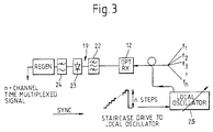
- the present invention is also applicable to fdm to tdm signal conversion in the optical domain, for example in an optical heterodyne coherent receiver, in which case the mixer comprises an optical detector which mixes a number of optical reference frequency signals from a variable local oscillator 25, a laser for example, with the received optical fdm signal from the secondary stations 6 - as shown in Figure 3.
- the mixer comprises an optical detector which mixes a number of optical reference frequency signals from a variable local oscillator 25, a laser for example, with the received optical fdm signal from the secondary stations 6 - as shown in Figure 3.
Abstract
Description
- The invention relates to apparatus and methods for converting a frequency division multiplex (fdm) signal into a time division multiplex (tdm) signal. It finds particular but not exclusive application in a communication system comprising a primary station and a plurality of secondary stations, each of the stations having signal transmitting means and signal receiving means, a first communication link extending from the primary station to signal splitting means for supplying signals from the primary station to each of the secondary stations, and a second communication link extending from signal combining means, which receives signals from each of the secondary stations, to the primary station.
- Such communication systems find application in a variety of fields including local telephone networks and the like. One method of operating such a communication system is to distribute signals from the primary station (or exchange) as a multiplex, for example a common time division multiplex signal, to all the secondary stations. Each station then selects the time slots appropriate to it. Although this is relatively straightforward, difficulties arise if the secondary stations are to transmit information back to the primary station by this method. In this case, the signals transmitted from the secondary stations must be accurately timed to avoid signal "collisions" in the common path back to the primary station. The timing will depend principally on the path length and, in the case of optical communication systems using optical fibres, this path length can vary slightly with temperature effects. Thus a ranging system must be built into each terminal.
- These difficulties can be obviated by combining the return signals from the secondary stations into a frequency division multiplex signal instead of attempting to combine these signals into a time division multiplex signal. This avoids the problems of timing due to variations in temperature and the like.
- Typically, the signals transmitted between the stations will comprise optical signals and in this case the stations may be coupled by optical waveguides such as optical fibres. However other media, including air, could define the communication links. Furthermore, the signals could comprise electrical or radio frequency signals.
- In some cases, separate paths may be provided between the primary station and the secondary stations to carry signals in respective directions. Conveniently, however, a common transmission path is used, for example a common optical waveguide in the case of optical signals. In the latter case the signal combining and splitting means are provided by a common element. In the case of a common transmission path, the signals could be transmitted with the same or different wavelengths in the opposite directions.
- The primary station receiving means may include a splitting means to split the incoming frequency division multiplex signal into a plurality of subsidiary signals, one for each secondary station, and a plurality of demodulating circuits for receiving respective ones of the subsidiary signals and for regenerating the information associated with the signal from the corresponding secondary station. However, this arrangement needs separate demodulating circuits for each channel or secondary station.
- British Patent Specification No. 1297922 discloses amplitude modulating an optical carrier signal by several radio frequency sub-carriers each modulated with lower frequency information bearing signals. At a receiving terminal the incoming optical signal is divided amonst n optical fibres each leading to its own respective receiver comprising a combined mixer and demodulator, a local oscillator, and an intermediate frequency (IF) amplifier. The outputs of all the channels, i.e. the IF amplifiers, are fed to a baseband detector for recovery of the information bearing signals.
- It is an object of the present invention to overcome the need for such separate demodulating circuits or separate receivers.
- Accordingly there is provided apparatus including a plurality of channels, each channel having a known common data rate, for converting a frequency division multiplex signal into a time division multiplex signal comprising a reference frequency signal generator for repeatedly generating a series of reference frequency signals in steps at a repetition rate synchronised to said known common data rate of the frequency division multiplex signal, the number of reference frequency signals being equal to the number of carrier signals in the frequency division multiplex signal; mixing means for mixing the frequency division multiplex signal and the reference frequency signals to generate intermediate frequency signals, the combination of respective pairs of carrier signals and reference frequency signals generating respective intermediate frequency signals at a common frequency; a bandpass filter for passing only the intermediate frequency signals at said common frequency from the output of the mixing means, the filter output thus constituting a time division multiplex signal in the form of a repeating corresponding series of respective intermediate frequency signals; and demodulating means responsive to the output from the bandpass filter for producing from the respective intermediate frequency signals corresponding channel data signals.
- Typically, the reference frequency signal generator will comprise a voltage controlled oscillator. The series of reference frequency signals may be generated in steps such that the repetition rate of the full staircase of reference frequency signals is preferably substantially twice the data rate. Other repetition rates are also possible.
- The generation of the intermediate frequency signals at a common frequency may be carried out in the electrical domain or in the optical domain, for example using a coherent optical heterodyne detection scheme in which the local optical oscillator is stepped through a staircase of optical reference frequency signals to be mixed with a received optical fdm signal.
- According to a second aspect of the invention there is provided a method of converting a frequency division multiplex signal including a plurality of channels, each channel having a known common data rate, into a time division multiplex signal, comprising repeatedly generating a series of reference frequency signals in steps at a repetition rate synchronised to said known common data rate, the number of reference frequency signals being equal to the number of carrier signals in the frequency division multiplex signal; mixing the frequency division multiplex signal and the reference frequency signals to generate respective intermediate frequency signals at a common frequency and demodulating the intermediate frequency signals at the common frequency to product corresponding channel data signals, which thus constitute a time division multiplex signal.
- According to a further aspect of the invention there is provided a communications system comprising a primary station; and a plurality of secondary stations, each of the stations having signal transmitting means and signal receiving means, a first communication link extending from the primary station to signal splitting means for supplying signals from the primary station to each of the secondary stations, and a second communication link extending from signal combining means, which receives signals from each of the secondary stations, to the primary station wherein the signal transmitting means of the primary station and the signal receiving means of the secondary stations are adapted to transmit and receive respectively multiplex signals, the signal transmitting means of the secondary stations are adapted to transmit signals at respective carrier frequencies, the signal combining means combining these signals into a common frequency division multiplex signal and the receiving means of the primary station is adapted to receive the common frequency division multiplex signal, the primary station including apparatus for converting the common frequency division multiplex signal into a time division multiplex according to the first aspect of the invention.
- Examples of such an apparatus, method and communication systems in accordance with the present invention will now be described with reference to the accompanying drawings, in which:-
- Figure 1 is a schematic block diagram of one example of a communication system;
- Figure 2 is a block diagram of a fdm to tdm converter according to the present invention; and
- Figure 3 is a schematic block diagram of an optical domain fdm to tdm converter according to the present invention.
- The communication system which is shown schematically in Figure 1 comprises a primary station or exchange 1 having an
optical transmitter 2 and areceiver 12. Thetransmitter 2 is connected to anelectrical signal multiplexer 4 which receives data signals on a plurality ofchannels 5, these signals being destined for respective ones of n terminals orsecondary stations 6. The data signals received by thesignal multiplexer 4 are multiplexed onto a common electrical signal in a time division manner and the time division multiplex signal is fed to anoptical transmitter 2. Thetransmitter 2 is modulated in accordance with the incoming electrical signal to generate a time division multiplex optical signal which is fed along an optical fibre 9 to anoptical fibre 10. Theoptical fibre 10 extends to anoptical splitter 11 which splits the incoming signal into a number of subsidiary signals, one for eachsecondary station 6. Eachstation 6 includes conventional demultiplexing circuitry to enable it to read the correct data contained within the time slots associated with that station. - When a
secondary station 6 wishes to transmit information back to the exchange 1, it generates an optical carrier signal with a frequency (fi) unique to that station which is modulated with the data. The modulated signal is fed along the same optical fibre as the incoming signal to theoptical splitter 11 which acts as a combiner to combine the signals from thestations 6 to form a frequency division multiplex signal which is fed back along theoptical fibre 10 to anoptical receiver 12 in the exchange 1. Thereceiver 12 converts the incoming optical signal into an electrical signal which is then fed to a fdm totdm converter 19 according to the present invention which will be now be described with reference to Figure 2. - Figure 2 illustrates the fdm to
tdm convertor 19 of a receiver shown in Figure 1. The frequency division multiplex signal is received by thereceiver 12, and fed to amixer circuit 20. The other input of themixer circuit 20 is connected to a voltage controlledoscillator 21 which is driven in a staircase manner, as shown in the drawing, so as to supply a series of different frequencies at stepped intervals to themixer circuit 20. - In practice, the transmitting
circuit secondary stations 6. Furthermore, thesecondary stations 6 will use the same clock signal when modulating their respective carrier signals to generate return signals and this enables theVCO 21 to be synchronised to the incoming signal. - The time period of each step in the staircase of the reference frequency signals may be selected as shown in Figure 2 selected so that the sweep frequency (i.e. repetition rate) of the full staircase of signals is twice or a higher integral of the data rate of the incoming signal and this defines the time period of each time division of the resultant time division multiplex signal. It may be necessary to adjust the phase of the individual return channels at the
secondary stations 6. - The reference frequency signals generated by the
VCO 21 are chosen such that the result of mixing each of these signals with a respective one only of the incoming carrier signals f₁-fn is a respective signal at a common intermediate frequency. The mixing of each reference frequency signal with the other carrier signals of the incoming signal will result in respective signals at intermediate frequencies different from the common intermediate frequency. - A
bandpass filter 22 is positioned downstream of themixer 20 to eliminate all signals but that at the common intermediate frequency which is then fed to ademodulator 23 whose output is fed to alowpass filter 24. The output from thelowpass filter 24 is an n-channel time division multiplex signal which can then be analysed in a conventional manner. - The primary station 1 may alternatively transmit frequency multiplexed signals to the
secondary stations 6, thestations 6 being provided with appropriate demultiplexers to enable them to select the signal at the appropriate frequency associated with the station. - It will be appreciated that apparatus for converting a fdm signal to a tdm signal according to the present invention can be employed with communications systems other than in the exemplary system shown in Figure 1.
- The present invention is also applicable to fdm to tdm signal conversion in the optical domain, for example in an optical heterodyne coherent receiver, in which case the mixer comprises an optical detector which mixes a number of optical reference frequency signals from a variable
local oscillator 25, a laser for example, with the received optical fdm signal from the secondary stations 6 - as shown in Figure 3.
Claims (10)
- Apparatus including a plurality of channels, each channel having a known common data rate, for converting a frequency division multiplex signal into a time division multiplex signal comprising a reference frequency signal generator (21; 25) for repeatedly generating a series of reference frequency signals in steps at a repetition rate synchronised to said known common data rate of the frequency division multiplex signal, the number of reference frequency signals being equal to the number of carrier signals in the frequency division multiplex signal; mixing means (20; 12) for mixing the frequency division multiplex signal and the reference frequency signals to generate intermediate frequency signals, the combination of respective pairs of carrier signals and reference frequency signals generating respective intermediate frequency signals at a common frequency; a bandpass filter (22) for passing only the intermediate frequency signals at said common frequency from the output of the mixing means, the filter output thus constituting a time division multiplex signal in the form of a repeating corresponding series of respective intermediate frequency signals; and demodulating means (23) responsive to the output from the bandpass filter for producing from the respective intermediate frequency signals corresponding channel data signals.
- Apparatus according to claim 1, wherein the repetition rate of the series of reference frequency signals generated by the reference frequency signal generator (21; 25) is substantially twice the data rate of the incoming frequency division multiplex signal.
- Apparatus according to either claim 1 or claim 2, in which the reference frequency signal generator (25) generates optical reference frequency signals.
- Apparatus system according to either claim 1 or claim 2, wherein the reference frequency signal generator (21) comprises a voltage controlled oscillator.
- A method of converting a frequency division multiplex signal including a plurality of channels, each channel having a known common data rate, into a time division multiplex signal, comprising repeatedly generating a series of reference frequency signals in steps at a repetition rate synchronised to said known common data, the number of reference frequency signals being equal to the number of carrier signals in the frequency division multiplex signal; mixing the frequency division multiplex signal and the reference frequency signals to generate intermediate frequency signals, the combination of respective pairs of carrier signals and reference frequency signals generating respective intermediate frequency signals at a common frequency; and demodulating the intermediate frequency signals at the common frequency to produce corresponding channel data signals, which thus constitute a time division multiplex signal.
- A method according to claim 5, wherein the repetition rate of the series of reference frequency signals is substantially twice the data rate.
- A method according to either claim 5 or claim 6, in which the reference frequency signal generator generates optical reference frequency signals and the mixing takes place in the optical domain.
- A communication system comprising a primary station (1); and a plurality of secondary stations (6), each of the stations having signal transmitting means (2) and signal receiving means (12, not shown), a first communication link (9, 10) extending from the primary station to signal splitting means (11) for supplying signals from the primary station (1) to each of the secondary stations (6), and a second communication link (10) extending from signal combining means (11), which receives signals from each of the secondary stations, to the primary station (6) wherein the signal transmitting means (2) of the primary station (1) and the signal receiving means (not shown) of the secondary stations (6) are adapted to transmit and receive respectively multiplex signals, the signal transmitting means of the secondary stations (6) are adapted to transmit signals at respective carrier frequencies, the signal combining means (11) combining these signals into a common frequency division multiplex signal and the receiving means (12) of the primary station (1) is adapted to receive the common frequency division multiplex signal, the primary station including apparatus (19) for converting the common frequency division multiplex signal into a time division multiplex signal as claimed in any one of claims 1 to 4.
- A system according to claim 8, in which the communication links (9, 10) comprise optical waveguides.
- A system according to either claim 8 or claim 9, wherein the signal splitting means and the signal combining means are provided by a common element (11), a common communication link (10) being provided between the common element and the primary station (1).
Applications Claiming Priority (2)
| Application Number | Priority Date | Filing Date | Title |
|---|---|---|---|
| GB878727847A GB8727847D0 (en) | 1987-11-27 | 1987-11-27 | Communication system |
| GB8727847 | 1987-11-27 |
Publications (2)
| Publication Number | Publication Date |
|---|---|
| EP0318334A1 EP0318334A1 (en) | 1989-05-31 |
| EP0318334B1 true EP0318334B1 (en) | 1994-11-30 |
Family
ID=10627658
Family Applications (1)
| Application Number | Title | Priority Date | Filing Date |
|---|---|---|---|
| EP88311257A Expired - Lifetime EP0318334B1 (en) | 1987-11-27 | 1988-11-28 | Apparatus and method for converting a frequency division multiplex to a time division multiplex |
Country Status (9)
| Country | Link |
|---|---|
| EP (1) | EP0318334B1 (en) |
| JP (1) | JP2694987B2 (en) |
| AT (1) | ATE114905T1 (en) |
| CA (1) | CA1334114C (en) |
| DE (1) | DE3852277T2 (en) |
| ES (1) | ES2064362T3 (en) |
| GB (1) | GB8727847D0 (en) |
| HK (1) | HK138096A (en) |
| WO (1) | WO1989005071A1 (en) |
Families Citing this family (1)
| Publication number | Priority date | Publication date | Assignee | Title |
|---|---|---|---|---|
| GB8921341D0 (en) * | 1989-09-21 | 1989-11-08 | Smiths Industries Plc | Optical multiplexing |
Family Cites Families (5)
| Publication number | Priority date | Publication date | Assignee | Title |
|---|---|---|---|---|
| GB1297922A (en) * | 1969-11-25 | 1972-11-29 | ||
| IT1159851B (en) * | 1978-06-20 | 1987-03-04 | Cselt Centro Studi Lab Telecom | IMPROVEMENTS IN WAVE LENGTH DIVISION TRANSMISSION SYSTEMS |
| US4302835A (en) * | 1980-01-24 | 1981-11-24 | Sperry Corporation | Multiple terminal passive multiplexing apparatus |
| DE3507064A1 (en) * | 1985-02-28 | 1986-08-28 | Standard Elektrik Lorenz Ag, 7000 Stuttgart | OPTICAL NEWS TRANSMISSION SYSTEM IN THE SUBSCRIBER AREA |
| JPH0669175B2 (en) * | 1986-04-30 | 1994-08-31 | シャープ株式会社 | Multi-frequency signal waveform processing method |
-
1987
- 1987-11-27 GB GB878727847A patent/GB8727847D0/en active Pending
-
1988
- 1988-11-25 CA CA000584226A patent/CA1334114C/en not_active Expired - Fee Related
- 1988-11-28 AT AT88311257T patent/ATE114905T1/en not_active IP Right Cessation
- 1988-11-28 WO PCT/GB1988/001039 patent/WO1989005071A1/en unknown
- 1988-11-28 DE DE3852277T patent/DE3852277T2/en not_active Expired - Fee Related
- 1988-11-28 ES ES88311257T patent/ES2064362T3/en not_active Expired - Lifetime
- 1988-11-28 EP EP88311257A patent/EP0318334B1/en not_active Expired - Lifetime
- 1988-11-28 JP JP63509473A patent/JP2694987B2/en not_active Expired - Lifetime
-
1996
- 1996-07-25 HK HK138096A patent/HK138096A/en not_active IP Right Cessation
Also Published As
| Publication number | Publication date |
|---|---|
| JPH03502751A (en) | 1991-06-20 |
| ATE114905T1 (en) | 1994-12-15 |
| DE3852277T2 (en) | 1995-04-06 |
| ES2064362T3 (en) | 1995-02-01 |
| JP2694987B2 (en) | 1997-12-24 |
| HK138096A (en) | 1996-08-02 |
| WO1989005071A1 (en) | 1989-06-01 |
| EP0318334A1 (en) | 1989-05-31 |
| DE3852277D1 (en) | 1995-01-12 |
| GB8727847D0 (en) | 1987-12-31 |
| CA1334114C (en) | 1995-01-24 |
Similar Documents
| Publication | Publication Date | Title |
|---|---|---|
| US5323255A (en) | Transceiver arrangement using TDM to transmit assigned subcarrier waveforms | |
| CA1199074A (en) | Communications network with optical channels | |
| US7151896B2 (en) | Burst optical communication apparatus | |
| US5546190A (en) | Carrier and clock recovery for lightwave systems | |
| US4754452A (en) | Optical local area network using a common optical carrier with separate user angle modulation | |
| JPS62206935A (en) | Optical communication equipment and optical signal transmission | |
| JP3000551B2 (en) | Photoelectric frequency divider circuit and method of operating the same | |
| CA1269159A (en) | Switching techniques for fdm communication systems | |
| WO1986005343A1 (en) | Line transmission systems | |
| US4402076A (en) | Two wire F.D. multiplex system | |
| US4414663A (en) | Time division multiplex system having transmitted pulses in time channels distributed over and co-transmitted with a frame clock signal component | |
| US5406553A (en) | Apparatus and method for converting a frequency division multiplex to a time division multiplex | |
| JP3512580B2 (en) | Optical transmitting apparatus and optical receiving apparatus for optical time division multiplex transmission, and optical time division multiplex optical transmission apparatus equipped with the same | |
| EP0318334B1 (en) | Apparatus and method for converting a frequency division multiplex to a time division multiplex | |
| US3450841A (en) | Carrier frequency stabilization for carrier frequency systems with suppressed carrier waves | |
| JPH05344095A (en) | Wavelength-clock synchronization system in optical communication network and wavelength multiplex optical communication network using the system | |
| JP3584072B2 (en) | Communication networks and stations | |
| JP2738542B2 (en) | Coherent optical communication system | |
| AU606241B2 (en) | Apparatus and method for converting a frequency division multiplex to a time division multiplex | |
| JPH1032563A (en) | Millimeter wave signal optical multiplex system and device | |
| JP3274873B2 (en) | Optical frequency relative positioning method and apparatus | |
| JP2003037868A (en) | Communication equipment | |
| RU2124812C1 (en) | Method for transmission of signals in digital fiber-optical systems using spectral-code multiplexing and device which implements said method | |
| JPH0563656A (en) | Wavelength synchronization type optical processing unit and optical path selector using the same unit | |
| JPH08213968A (en) | Optical wavelength multiplex communication system |
Legal Events
| Date | Code | Title | Description |
|---|---|---|---|
| PUAI | Public reference made under article 153(3) epc to a published international application that has entered the european phase |
Free format text: ORIGINAL CODE: 0009012 |
|
| AK | Designated contracting states |
Kind code of ref document: A1 Designated state(s): AT BE CH DE ES FR GB GR IT LI LU NL SE |
|
| 17P | Request for examination filed |
Effective date: 19891107 |
|
| 17Q | First examination report despatched |
Effective date: 19911024 |
|
| GRAA | (expected) grant |
Free format text: ORIGINAL CODE: 0009210 |
|
| AK | Designated contracting states |
Kind code of ref document: B1 Designated state(s): AT BE CH DE ES FR GB GR IT LI LU NL SE |
|
| PG25 | Lapsed in a contracting state [announced via postgrant information from national office to epo] |
Ref country code: AT Effective date: 19941130 Ref country code: LI Effective date: 19941130 Ref country code: GR Free format text: LAPSE BECAUSE OF FAILURE TO SUBMIT A TRANSLATION OF THE DESCRIPTION OR TO PAY THE FEE WITHIN THE PRESCRIBED TIME-LIMIT Effective date: 19941130 Ref country code: BE Effective date: 19941130 Ref country code: CH Effective date: 19941130 |
|
| REF | Corresponds to: |
Ref document number: 114905 Country of ref document: AT Date of ref document: 19941215 Kind code of ref document: T |
|
| REF | Corresponds to: |
Ref document number: 3852277 Country of ref document: DE Date of ref document: 19950112 |
|
| EAL | Se: european patent in force in sweden |
Ref document number: 88311257.5 |
|
| ITF | It: translation for a ep patent filed |
Owner name: JACOBACCI & PERANI S.P.A. |
|
| REG | Reference to a national code |
Ref country code: ES Ref legal event code: FG2A Ref document number: 2064362 Country of ref document: ES Kind code of ref document: T3 |
|
| REG | Reference to a national code |
Ref country code: CH Ref legal event code: PL |
|
| ET | Fr: translation filed | ||
| PLBE | No opposition filed within time limit |
Free format text: ORIGINAL CODE: 0009261 |
|
| STAA | Information on the status of an ep patent application or granted ep patent |
Free format text: STATUS: NO OPPOSITION FILED WITHIN TIME LIMIT |
|
| 26N | No opposition filed | ||
| PG25 | Lapsed in a contracting state [announced via postgrant information from national office to epo] |
Ref country code: LU Free format text: LAPSE BECAUSE OF NON-PAYMENT OF DUE FEES Effective date: 19951130 |
|
| PGFP | Annual fee paid to national office [announced via postgrant information from national office to epo] |
Ref country code: SE Payment date: 20001016 Year of fee payment: 13 |
|
| PGFP | Annual fee paid to national office [announced via postgrant information from national office to epo] |
Ref country code: NL Payment date: 20001020 Year of fee payment: 13 |
|
| PGFP | Annual fee paid to national office [announced via postgrant information from national office to epo] |
Ref country code: ES Payment date: 20001107 Year of fee payment: 13 |
|
| PGFP | Annual fee paid to national office [announced via postgrant information from national office to epo] |
Ref country code: FR Payment date: 20011012 Year of fee payment: 14 |
|
| PGFP | Annual fee paid to national office [announced via postgrant information from national office to epo] |
Ref country code: DE Payment date: 20011029 Year of fee payment: 14 |
|
| PG25 | Lapsed in a contracting state [announced via postgrant information from national office to epo] |
Ref country code: ES Free format text: LAPSE BECAUSE OF NON-PAYMENT OF DUE FEES Effective date: 20011129 Ref country code: SE Free format text: LAPSE BECAUSE OF NON-PAYMENT OF DUE FEES Effective date: 20011129 |
|
| REG | Reference to a national code |
Ref country code: GB Ref legal event code: IF02 |
|
| PG25 | Lapsed in a contracting state [announced via postgrant information from national office to epo] |
Ref country code: NL Free format text: LAPSE BECAUSE OF NON-PAYMENT OF DUE FEES Effective date: 20020601 |
|
| EUG | Se: european patent has lapsed |
Ref document number: 88311257.5 |
|
| NLV4 | Nl: lapsed or anulled due to non-payment of the annual fee |
Effective date: 20020601 |
|
| PG25 | Lapsed in a contracting state [announced via postgrant information from national office to epo] |
Ref country code: DE Free format text: LAPSE BECAUSE OF NON-PAYMENT OF DUE FEES Effective date: 20030603 |
|
| PG25 | Lapsed in a contracting state [announced via postgrant information from national office to epo] |
Ref country code: FR Free format text: LAPSE BECAUSE OF NON-PAYMENT OF DUE FEES Effective date: 20030731 |
|
| REG | Reference to a national code |
Ref country code: FR Ref legal event code: ST |
|
| REG | Reference to a national code |
Ref country code: ES Ref legal event code: FD2A Effective date: 20021213 |
|
| PG25 | Lapsed in a contracting state [announced via postgrant information from national office to epo] |
Ref country code: IT Free format text: LAPSE BECAUSE OF NON-PAYMENT OF DUE FEES Effective date: 20051128 |
|
| PGFP | Annual fee paid to national office [announced via postgrant information from national office to epo] |
Ref country code: GB Payment date: 20071018 Year of fee payment: 20 |
|
| REG | Reference to a national code |
Ref country code: GB Ref legal event code: PE20 Expiry date: 20081127 |
|
| PG25 | Lapsed in a contracting state [announced via postgrant information from national office to epo] |
Ref country code: GB Free format text: LAPSE BECAUSE OF EXPIRATION OF PROTECTION Effective date: 20081127 |