EP0307945A2 - Memory control apparatus for use in a data processing system - Google Patents
Memory control apparatus for use in a data processing system Download PDFInfo
- Publication number
- EP0307945A2 EP0307945A2 EP88115235A EP88115235A EP0307945A2 EP 0307945 A2 EP0307945 A2 EP 0307945A2 EP 88115235 A EP88115235 A EP 88115235A EP 88115235 A EP88115235 A EP 88115235A EP 0307945 A2 EP0307945 A2 EP 0307945A2
- Authority
- EP
- European Patent Office
- Prior art keywords
- memory
- bus
- access
- control apparatus
- data
- Prior art date
- Legal status (The legal status is an assumption and is not a legal conclusion. Google has not performed a legal analysis and makes no representation as to the accuracy of the status listed.)
- Granted
Links
Images

Classifications
-
- G—PHYSICS
- G11—INFORMATION STORAGE
- G11C—STATIC STORES
- G11C8/00—Arrangements for selecting an address in a digital store
- G11C8/12—Group selection circuits, e.g. for memory block selection, chip selection, array selection
-
- G—PHYSICS
- G11—INFORMATION STORAGE
- G11C—STATIC STORES
- G11C11/00—Digital stores characterised by the use of particular electric or magnetic storage elements; Storage elements therefor
- G11C11/21—Digital stores characterised by the use of particular electric or magnetic storage elements; Storage elements therefor using electric elements
- G11C11/34—Digital stores characterised by the use of particular electric or magnetic storage elements; Storage elements therefor using electric elements using semiconductor devices
- G11C11/40—Digital stores characterised by the use of particular electric or magnetic storage elements; Storage elements therefor using electric elements using semiconductor devices using transistors
- G11C11/401—Digital stores characterised by the use of particular electric or magnetic storage elements; Storage elements therefor using electric elements using semiconductor devices using transistors forming cells needing refreshing or charge regeneration, i.e. dynamic cells
- G11C11/406—Management or control of the refreshing or charge-regeneration cycles
-
- G—PHYSICS
- G11—INFORMATION STORAGE
- G11C—STATIC STORES
- G11C7/00—Arrangements for writing information into, or reading information out from, a digital store
- G11C7/10—Input/output [I/O] data interface arrangements, e.g. I/O data control circuits, I/O data buffers
- G11C7/1015—Read-write modes for single port memories, i.e. having either a random port or a serial port
- G11C7/1018—Serial bit line access mode, e.g. using bit line address shift registers, bit line address counters, bit line burst counters
- G11C7/1021—Page serial bit line access mode, i.e. using an enabled row address stroke pulse with its associated word line address and a sequence of enabled column address stroke pulses each with its associated bit line address
Definitions
- This invention relates generally to digital computers and, in particular, relates to a digital computer system having a system bus for interconnecting various agents and a page mode memory access for transferring blocks of data between agents.
- This invention provides a computer bus having page mode memory acces.
- Modern computer systems are often characterized by a plurality of functionally differenct types of circuit cards, or agents, which are interconnected by means of a system bus.
- a system bus In order to facilitate the design of such circuit cards and the implementation of software routines necessary to utilize these cards such computer buses are typically standardized.
- One such bus is a 32-bit high performance synchronous bus known as the P1296, which is also commonly known as Multibus II.
- Such a bus typically comprises a plurality of predefined signal lines which are utilized for the transfer of memory addresses and data between two or more circuit boards which are interconnected to the bus. Other signal lines are defined for regulating the transfer of data over the bus, for interrupt events, and for error conditions. Also, one or more clocks are provided by the bus for synchronizing the flow of data between agents.
- a bus will have interconnected thereto at least one circuit card having a data processor contained thereon, such as a microprocessor device.
- Other circuit cards may comprise input/output (I/O) circuitry for interfacing to external devices such as mass storage devices, CRTs and printers.
- Other cards interconnected to the bus may be high capacity memory cards which comprise a plurality of read/write memories such as dynamic random access memories (DRAM) which are operable for the storage and retrieval of data.
- DRAM dynamic random access memories
- a circuit card such as a card adapted for control of a mass storage device may also have a relatively large amount of DRAM for local buffering of data going to and coming from the mass storage device and may also have a local microprocessor device for controlling the mass storage device.
- bus may be considered to be a shared resource which is common to all of the circuit cards which are interconnected to the bus, it is desirable that such data transfers occur in a rapid manner to avoid a reduction in the bandwidth of the bus.
- a first in/first out (FIFO) buffer upon both a requesting agent and a relying agent.
- the requesting agent may notify the relying agent that it desires a block of data to be read from a local memory on the replying agent and thereafter transmitted to the requesting agent over the bus.
- the replying agent accesses the desired memory locations and loads the data contained therein into the replying angent's FIFO, the data thereafter being transmitted from the FIFO across the bus to a FIFO on the requesting agent from where the requesting agent may extract and store the data in a local memory.
- the use of such FIFO buffers may result in the system incurring additional costs and complexity.
- the storage capacity of available FIFO buffers may be insufficient to transfer a desired block size of data, resulting in the requirement that the FIFO be fully loaded two or more times with data.
- memory interleaving In other systems it has been known to utilize memory interleaving in order to increase the data transfer speed of the bus. Memory interleaving however may also result in an increased system cost. Also, memory interleaving may increase the speed of only certain types of data transfers.
- the problem of achieving or maintaining a high bus bandwidth is also related to a requirement that the memory devices, if they are DRAM devices, be periodically refreshed. This refresh requirement may result in the need to interrupt a block data transfer in order to accomplish the refresh. Also, if a local processor is included on the agent, the local processor may also require access to the memory, thereby also interfering with the transfer of data between agents.
- a memory control apparatus for use in a data processing system having at least a requesting agent and a replying agent electrically coupled together by a system bus, the requesting agent requesting access to a memory on the replying agent for storing and retrieving data therein over the system bus.
- the claimed memory control apparatus comprises means for detecting a request for initiating an access cycle to a memory on the replying agent; means, responsive to the request detecting means, for asserting a plurality of memory address control signals for successively accessing the memory on the replying agent, the control signals comprising at least a row address strobe associated with a row address and a column address strobe associated with a column address; and means for detecting a completion of the access cycle to the memory, the completion detecting means being responsive to a logic state of an end of cycle control signal generated by the requesting agent.
- the asserting means asserts the memory address control signals by asserting the row address strobe signal a plurality of times in conjunction with a row address being indicative of a page of data within the memory, and thereafter asserts and deasserts the column address strobe signal in conjunction with a plurality of column addresses for performing a page mode type of memory access.
- a method for controlling a memory for use in a data processing system having at least a requesting agent and a replying agent electrically coupled together by a system bus, the requesting agent requesting access to a memory on the replying agent for storing and retrieving data therein over the system bus, the method comprising the steps of detecting a request for initiating an access cycle to a memory on the replying agent; asserting a plurality of memory address control signals for accessing the memory on the replying agent, the control signals comprising at least a row address strobe associated with a row address and a column address strobe associated with a column address; detecting a completion of the accesss cycle to the memory, the completion detecting means being responsive to a logic state of an end of cycle control signal generated by the requesting agent; and wherein the step of asserting is accomplished by asserting the row address strobe signal in conjunction with a row address being indicative of a page of data within the memory, and thereafter asserting and deasser
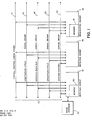
- a requesting agent 12 and replying agents 14 and 16 are bidirectionally coupled to the bus 10.
- the requesting agent 12 may have a local memory 18 which may be comprised of dynamic random access memories (DRAM).
- the replying agent 16 is also shown to have a local memory 20 which may be similarly comprised of DRAM.
- a mass storage device 22 which may comprise a familiar Winchester or floppy magnetic disk for the mass storage of data and program information.
- a digital computer system may have a plurality of requesting agents and a plurality of replying agents coupled to the bus. It should further be realized that at one time in the operation of the system 1 that the requesting agent 12 may be a replying agent, and that the replying agent 16 may at that time be a requesting agent.
- the characterization of an agent as being either a replying agent or a requesting agent is accomplished by means of certain bus signals which will be described below.
- the requesting agent 12 may be a central computer board and the replying agent 16 may be a disk controlling board which stores and retrieves document data from the mass storage device 22.
- the replying agent 16 may be a disk controlling board which stores and retrieves document data from the mass storage device 22.
- an operator may interact via a keyboard or some other means with a program on the central computer board, the program embodying a word procesing program wherein the operator enters document data which is stored on mass storage 22.
- document data may be organized as pages of data it can be appreciated that a certain block size of data may be utilized to represent a visually displayed page of a document, such as 2K bytes of data.
- Bus 10 may compise 96 conductor lines, which are subdivided into groups having different functionality.
- a central control signal group 24 provides system-wide signals such as reset and initialization control signals.
- ther are defined eight central control signals, some of which are a reset signal for initializing the system and two clock signals, namely a bus clock (BCLK*) and a central clock (CCLK*).
- a third clock signal such as a system clock (SCLK*) 24a (shown in Fig. 5).
- SCLK* system clock
- the Multibuss II specifies that CCLK* should be twice the frequency of BCLK*, with data transfers across the bus requiring one BCLK* cycle.
- BCLK* is 10 MZH
- CCLK* is 20 MHZ
- a bus data transfer requires 200 nanoseconds.
- SCLK* higher frequency clock signal
- SCLK* 24a operating at 20 MHZ
- the arbitration cycle signal group 26 is comprised of seven signal lines, one being a bus request (BREQ*) which is wire ORED between each of the agents on the bus. Any agent requiring access to the bus 10 must assert BREQ* in order to be granted access, the access typically being granted by an arbitration logic circuit chich is not shown in Fig. 1.
- Six arbitration identification signals, ARBO*-ARB5*, are driven by an agent or agents which require access to the bus, these signals being inputs to the arbitration controller.
- the address/data bus signal group 28 provides address, data and parity signals for data read and write bus transfers. There are a total of 36 address/data bus signals, characterized as 32 multiplexed address/data bus signals (AD0*-AD31*) and four parity signals associated with bytes of data, namely PAR0*-PAR3*.
- the exception cycle signal group 30 provides error detection which is utilized to terminate a bus transfer cycle.
- Ther are two exception cycle signals, a bus error signal (BUSERR*) and a time out signal (TIMOUT*).
- a system control signal group 32 provides control signals which are utilized to transfer addresses and data over the bus.
- the Multibus II there are 10 system control signals SC0*-SC9*.
- SC0*-SC9* During a request phase of a bus transfer cycle the requesting agent 12 drives SC0* through SC9* to provide command information to the replying agent, such as a the replying agent 16.
- the reply phase of the bus transfer cycle the requesting agent drives SC9* and SC0*-Sc3* while the replying agent drives SC8* and SC4*-SC7* in order to provide handshaking and status information between the requesting and replying agents.
- the Multibus II supports a plurality of different types of data transfers such as message types. These message types may be a plurality of unsolicited message type. Additionally, memory space data transfers may occur. Data transfers of up to 64K bytes are supported by the bus. However, in many conventional systems bus data transfers are limited to 32 byte packets.
- a first in/first out (FIFO) buffer is typically utilized on each agent, the FIFO buffer being fully loaded with data on the replying agent, the data terheafter being transferred to the bus 10 where it is received by a FIFO buffer on the requesting agent. As has been previously described, the use of such FIFO buffers may result in increased system cost and complexity. Additionally, a significant amount of time is required to fully load and unload the FIFO buffers.
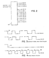
- a well known DRAM having a Data In and a Data Out signal line and a plurality of address lines AD0 through AD8.
- the DRAM 40 also has a Ras*, CAS*, and a R/W signal control line.
- such DRAMs typically multiplex the address lines such that at one time in the operation of the device the address lines are characterized as row address lines under the control of Ras* and at another time in th cycle are characteized as column address lines under the conrol of Cas*.
- DRAM 2 has nine address signal pins and, thus, has a total of 18 address inputs which yeild a device having a total of 256K bit storage locations.
- other DRAMs may have more or less than nine address inputs such as 64K and 1M bit devices and other devices may store more than one bit of data, such as devices adapted to simultaniously store and retrieve four bits of data.
- the conventional addressing mode for such a DRAM results in Ras* being asserted 42 for latching within the RAM the row address lines appearing on AD0-AD8. Subsequent to the assertion of Ras* the state ofthe address lines AD0-AD8 are switched to the desired column address and Cas* is asserted 44. The assertion of Cas* also typically either stores within the device or reads from the device, depending upon the state of R/W*, a bit of data at the specified row and column address.
- Fig. 4 there is shown another type of addressing node known as a page mode type of access wherein Ras* is asserted once at 46 to latch the row address within the device. Thereafter, the column address may be repeatedly varied and Cas* may be asserted a plurality of times (48-58) in order to store or retrieve data.
- the row address lines can be considered to define a page of data bits within the device, multiple assertions of Cas* can be utilized to Scroll" through the page of data in a significantly more rapid manner than the conventional Ras*-Cas* type of cycle.
- Such a page mode access is made espedcially convenient if the data is accessed sequentially, that is, if the column address is incremented or decremented by one for each access.
- non-sequential page mode access is also possible and may be desirable for some applications.
- this page mode type of access cycle is advantageously employed to increase the bandwidth of the system bus for at least the memory space type of data transfer.
- the delays incurred by the assertion of Ras* for each memory access often require that the aforementioned FIFO buffer be utilized to temporarily buffer data.
- a much faster memory access cycle is achieved by employing the page mode type of access, thereby eliminating the need for local buffer storage of incoming or outgoing data in order to maintain a desired bus bandwidth.
- a memory 60 is comprised of two banks of memory devices, such as DRAM devices, organized as a Bank 1 62 and a Bank 2 64. Selection between banks is made by Ras0* and Ras1* signal lines which are inputs to Bank 1 and Bank 2, respectively.
- Each of the Banks 62 and 64 is comprised of four subbanks of memory devices organized as bytes. Selection of a particular byte within a Bank is made by the state of the Cas0*-Cas3* signal lines.
- the particular mode of addressing is determined by the state of the A0, A1, W0 and W1 signal lines which are inputs to a memory controller 66, these signal lines being, for example, various address signals of the Memory Address Bus 68 and control signals of the system control signal group 32.
- the states of the aforementioned signals are decoded by a decoder 70 associated with memory controller 66 to select both the width of the memory transfer and also th columns of memory devices which are selected.
- Truth tables which describe the operation of decoder 70 are given below.
- An R0 input to memory controller 66 may also be an address line, the state of which selects either Bank 1 or Bank 2 for access via Ras0* or Ras1*.
- a request/acknowledge (R/A) input signal is a bidirectional signal which is normally an input to memory controller 66 when the controller 66 is in a quiescent operating state.
- the R/A signal line may be pulsed low by external logic (not shown). After making such a request for memory access the R/A signal line may be released by the external logic such that it may be driven by controller 66 during the memory request acknowledge cycle.
- the request memory controller 66 accesses the memory 60 in accordance with the states of the A0, A1, W0, W1 and R0 lines in conjunction with the state of the Read/Write (RW) input.
- Memory controller 66 then drives R/A to a logic low signal level to acknowledge the memory access. After initiating a memory access the memory controller 66 accesses the memory repeatedly until an EOC signal line (bus signal SC2*) is asserted for indicating an End of Cycle condition. When EOC is asserted the memory controller 66 is informed that the current memory access is the final memory access of the reply phase of the sequential data transfer.
- EOC EOC signal line
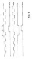
- Fig. 6 there is shown a timing diagram which illustrates a portion of consecutive memory accesses made by controller 66 to memory 60 during the reply phase of a sequential data transfer.
- the R/A signal line is driven low by controller 66 and therafter released.
- the Ras* line is maintained in an asserted, or low state, and the Cas* line is repeatedly toggled to achieve a page mode memory access cycle.
- the SC4* signal line is asserted by memory controller 66 for notifying the requesting agent that the replier ready condition exists, that is, that the memory controller 66 is accessing data for the requester.
- a DENO signal line output by the memory controller may be utilized, when data is being read from memory 60, to enable a buffer 72 for placing the data from the Memory Data Bus 74 onto the system bus 10.
- the page mode type of memory access which is a feature of the invention, advantageously provides for a high bus bandwidth.
- the Ras* signal line is not required to be driven for each memory access, the additional delay incurred by the assertion of Ras* in conjunction with each Cas* is eliminated, thereby increasing the speed of the overall transfer of a block of data to or from the memory 60.
- a given page of data is characterized by the nine row address lines associated with the Ras* signal.
- the DRAM can be seen to comprise 512 pages of data.
- each page has 512 storage locations, due to the nine column address lines associated with the Cas* signal. If a desired block size of data exceeds 512 bytes it is necessary to access more than one page of data within the device. In accordance with the invention, this is accomplished by a memory column address decoder 76 which may be a nand gage having nine inputs for detecting when the column address lines are each at a logic one condition.
- the output of the decoder 76 is a Page Crossing Detect (PC) signal which is an input to the memory controller 66.
- PC Page Crossing Detect
- Fig. 6 This is illustrated in Fig. 6 at time T1 where PC* is driven low by the decoder 76.
- the Ras* signal line is driven high by memory controller 66 in conjunction with the R/A signal and also SC4*.
- This operation of memory controller 66 notifies the agent receiving data, via the deassertion of the replier ready handshaking signal SC4*, that the replier is no longer in a ready condition.
- the row address whithin address latch 77 is, for example, incremented by 1 to select the next consecutive page of data within the memory devices.
- RAS* is asserted, thereby latching the new row address into the memory devices and the page mode memory access cycles begin as before, the SC4* line being once more asserted and R/A being once more driven to a low state.
- the refresh of DRAM within the memory 60 may be accomplished by a blocked refresh technique.
- a timer 78 generates refresh requests at predetermined intervals, such as a refresh request every 13.8 microseconds.
- the refresh requests are counted by a refresh request counter 80 and a comparator 82 determines when the number of counted refresh requests equal or exceed a predetermined threshold value, such as 24.
- a predetermined threshold value such as 24.
- controller 66 will attempt to burst refresh all of the 24 pending requests. If, however, there is a bus transfer in progress the memory controller 66 will not per form the burst refresh.
- the memory controller 66 will attempt to wait until the bus transfer is completed, that is, a transfer has occurred wherein EOC is asserted.
- the bus transfer is interrupted and the burst refresh is performed.
- the bus transfer is interrupted all of the pending refreshes are performed.
- the particular numbers chosen as the pending refresh threshold and the maximum number of pending refreshes are determined such that the amount of time represented by the difference between the threshold and the maximum values is a sufficient amount of time within which to transfer some predetermined block size of data. For example, for a refresh request made every 13.8 microseconds the difference between 24 and 41 refresh requests is approximately 234.5 microseconds which, it has been found, is a sufficient amount of time to complete a 2K byte (2048 bytes) bus transfer operation.
- a refresh acknowledge (RACK) signal is generated by a refresh controller 83, the RACK signal enabling a refreesh row counter 84 to place the refresh row addresses on the memory address bus.
- RACK is subsequently toggled between a high and a low state under the control of controller 83 for, as an example, 24 cycles in order to burst refresh 24 row addresses.
- the RAS0* and RAS1* signals are preferably both asserted to refresh simultaneously both banks of memory.
- the refresh row counter 84 may be incremented by the rising edge of th RACK signal such that at the completion of each refresh cycle counter 84 has a value corresponding to the next row address to be refreshed.
- a local processor 86 may also have access to the memory 60 via separate address and data latches 88 and 90, respectively.
- Local processor 86 may also be serviced by a dedicated memory controller (not shown) operable for generating memory access signals.
- a dedicated memory controller not shown
- AEN1 signal is driven to enable the address and datat latches of the local processor onto the memory address and memory data buses 68 and 70, respectively.
- the local processor is also proved with a High Priority (HP) signal which is an input to the memory controller 66 to interrupt, if necessary, a current bus transfer.
- HP High Priority
- the HP signal therefore allows the local processor to gain access to the memories by overriding a current bus transfer.
- the HP signal will override the current bus transfer for as long as it is asserted, thereby allowing the local processor 86 to make a number of consecutive high priority accesses to the memory 60.
- the aforedescribed blocked refresh operates somewhat differently if a series of high priority local processor memory accesses are in progress. As described previously, the memory controller 66 will accumulate pending refresh requests up to a maximum number of 41. If a high priority access is in progress at this time, the high priority access will be temporarily overridden but only two memory refreshes will take place. Thus, the high priority access by the local processor is suspended for only a relatively brief peeriod of time before the local processor is once again granted access to the memory 60. Of course, after the two refreshes are accomplished the counter 80 will continue to accumulate refresh requests such that when the counter once again reaches 41 and, if the high priority access is still in progress, the memory controller will once again suspend the high priority access and burst refresh to the next consecutive two row addresses.
- the operation of the aforedescribed blocked burst refresh and high priority request are shown in the waveforms of Figs. 7 and 8.
- the foregoing description of the memory controller 66 and the associated circuitry is illustrative and that a number of different embodiments may occur to those skilled in this art.
- the aforedescribed functions of the memory controller 66 may be accomplished by a plurality of discrete logic devices or, prefereably, may be embodied wihtin a LISI semiconductor device.
- the various elements associated with memory controller 66 may or may not be included within such an LSI device.
- the timer 74 may be external to the device as may be the refresh request counter 80.
- the memory controller 66 may operate with still other devices which are adapted for monitoring and controlling the system bus 10 activity, such as a device operable for asserting R/A when a request is made by anothe agent on the bus 10 for access to the memory 60.
- the SC3* and SC4* signal lines may not be tied directly from the bus 10 to the memory controller but may be buffered or therwise modified by other logic devices.
Landscapes
- Engineering & Computer Science (AREA)
- Microelectronics & Electronic Packaging (AREA)
- Computer Hardware Design (AREA)
- Dram (AREA)
- Memory System (AREA)
- Bus Control (AREA)
Abstract
Description
- This invention relates generally to digital computers and, in particular, relates to a digital computer system having a system bus for interconnecting various agents and a page mode memory access for transferring blocks of data between agents.
- This invention provides a computer bus having page mode memory acces.
- Modern computer systems are often characterized by a plurality of functionally differenct types of circuit cards, or agents, which are interconnected by means of a system bus. In order to facilitate the design of such circuit cards and the implementation of software routines necessary to utilize these cards such computer buses are typically standardized. One such bus is a 32-bit high performance synchronous bus known as the P1296, which is also commonly known as Multibus II.
- Such a bus typically comprises a plurality of predefined signal lines which are utilized for the transfer of memory addresses and data between two or more circuit boards which are interconnected to the bus. Other signal lines are defined for regulating the transfer of data over the bus, for interrupt events, and for error conditions. Also, one or more clocks are provided by the bus for synchronizing the flow of data between agents. Typically, such a bus will have interconnected thereto at least one circuit card having a data processor contained thereon, such as a microprocessor device. Other circuit cards may comprise input/output (I/O) circuitry for interfacing to external devices such as mass storage devices, CRTs and printers. Other cards interconnected to the bus may be high capacity memory cards which comprise a plurality of read/write memories such as dynamic random access memories (DRAM) which are operable for the storage and retrieval of data. Additionally, a circuit card such as a card adapted for control of a mass storage device may also have a relatively large amount of DRAM for local buffering of data going to and coming from the mass storage device and may also have a local microprocessor device for controlling the mass storage device.
- A problem arises when it is desired to transfer relatively large blocks of data betwen circuit cards on such bus. Inasmuch as the bus may be considered to be a shared resource which is common to all of the circuit cards which are interconnected to the bus, it is desirable that such data transfers occur in a rapid manner to avoid a reduction in the bandwidth of the bus.
- In order to achieve an increased bus bandwidth it has been known to provide a first in/first out (FIFO) buffer upon both a requesting agent and a relying agent. For example, the requesting agent may notify the relying agent that it desires a block of data to be read from a local memory on the replying agent and thereafter transmitted to the requesting agent over the bus. In response thereto the replying agent accesses the desired memory locations and loads the data contained therein into the replying angent's FIFO, the data thereafter being transmitted from the FIFO across the bus to a FIFO on the requesting agent from where the requesting agent may extract and store the data in a local memory. As can be appreciated, the use of such FIFO buffers may result in the system incurring additional costs and complexity. Furthermore, the storage capacity of available FIFO buffers may be insufficient to transfer a desired block size of data, resulting in the requirement that the FIFO be fully loaded two or more times with data.
- In other systems it has been known to utilize memory interleaving in order to increase the data transfer speed of the bus. Memory interleaving however may also result in an increased system cost. Also, memory interleaving may increase the speed of only certain types of data transfers.
- The problem of achieving or maintaining a high bus bandwidth is also related to a requirement that the memory devices, if they are DRAM devices, be periodically refreshed. This refresh requirement may result in the need to interrupt a block data transfer in order to accomplish the refresh. Also, if a local processor is included on the agent, the local processor may also require access to the memory, thereby also interfering with the transfer of data between agents.
- The foregoing problems are overcome and other advantages are realized by a memory control apparatus for use in a data processing system having at least a requesting agent and a replying agent electrically coupled together by a system bus, the requesting agent requesting access to a memory on the replying agent for storing and retrieving data therein over the system bus. The claimed memory control apparatus comprises means for detecting a request for initiating an access cycle to a memory on the replying agent; means, responsive to the request detecting means, for asserting a plurality of memory address control signals for successively accessing the memory on the replying agent, the control signals comprising at least a row address strobe associated with a row address and a column address strobe associated with a column address; and means for detecting a completion of the access cycle to the memory, the completion detecting means being responsive to a logic state of an end of cycle control signal generated by the requesting agent. In accordance with the invention the asserting means asserts the memory address control signals by asserting the row address strobe signal a plurality of times in conjunction with a row address being indicative of a page of data within the memory, and thereafter asserts and deasserts the column address strobe signal in conjunction with a plurality of column addresses for performing a page mode type of memory access.
- In accordance with a method of the invention there is disclosed a method for controlling a memory for use in a data processing system having at least a requesting agent and a replying agent electrically coupled together by a system bus, the requesting agent requesting access to a memory on the replying agent for storing and retrieving data therein over the system bus, the method comprising the steps of detecting a request for initiating an access cycle to a memory on the replying agent; asserting a plurality of memory address control signals for accessing the memory on the replying agent, the control signals comprising at least a row address strobe associated with a row address and a column address strobe associated with a column address; detecting a completion of the accesss cycle to the memory, the completion detecting means being responsive to a logic state of an end of cycle control signal generated by the requesting agent; and wherein the step of asserting is accomplished by asserting the row address strobe signal in conjunction with a row address being indicative of a page of data within the memory, and thereafter asserting and deasserting the column address strobe signal in conjunction with a plurality of colyumn addresses for performing a page mode type of memory access.
- The foregoing aspects of the invention will be more fully described below in the detailed description of the invention, the description being read in conjuntion with the drawings wherein:
- Fig. 1 is a block diagram of a
system bus 10 having a plurality of agents coupled thereto illustrating various types of signal groups which comprise thebus 10; - Fig. 2 is a block diagram of a typical DRAM which may be employed upon an agent coupled to the
bus 10; - Fig. 3 is a simplified timing diagram showing typical Ras* - Cas* memory access cycles which may be employed to access the DRAM of Fig. 2;
- Fig 4. is a simplified timing diagram showing page mode memory access cycles which are one feature of the invention;
- Fig. 5 is a block diagram which illustrates a
memory controller 66 and other circiutry coupled to amemory 60; - Fig. 6 is a timing diagram which shows the result of the detection of a page crossing signal;
- Fig. 7 is a timing diagram which shows a burst refresh of the
memory 60; and - Fig. 8 is a timing diagram which shows the refresh of the
memory 60 during a high priority local processor access. - Although the method and apparatus of the invention will be described herein in the context of a Multibus II environment, it should be appreciated that the invention may be practiced in many digital computer systems having a bus for transferring data between at least two agents interconnected upon the bus.
- The operating characteristics of the Multibus II are described in a document entitled "High Performance 32-Bit Bus Standard P1296" which was produced by the IEEE microprocessor standards committee P1296 working group, June 20, 1986, draft 2.0, the disclosure of which is incorporated herein in its entirety.
- Referring now to Fig. 1 there is shown in block diagram form a portion of a
digital computer system 1 comprising abus 10 and a plurality of agents 12-14 connected thereto. As shown in Fig. 1 a requestingagent 12 and replyingagents bus 10. The requestingagent 12 may have alocal memory 18 which may be comprised of dynamic random access memories (DRAM). The replyingagent 16 is also shown to have alocal memory 20 which may be similarly comprised of DRAM. Also coupled to replyingagent 16 is amass storage device 22 which may comprise a familiar Winchester or floppy magnetic disk for the mass storage of data and program information. - Although one requesting
agen 12 and two replyingagents system 1 that the requestingagent 12 may be a replying agent, and that the replyingagent 16 may at that time be a requesting agent. The characterization of an agent as being either a replying agent or a requesting agent is accomplished by means of certain bus signals which will be described below. - As an example of the operation of such a system, if the
system 1 is a word processing system the requestingagent 12 may be a central computer board and the replyingagent 16 may be a disk controlling board which stores and retrieves document data from themass storage device 22. In such a system an operator may interact via a keyboard or some other means with a program on the central computer board, the program embodying a word procesing program wherein the operator enters document data which is stored onmass storage 22. Inasmuch as such document data may be organized as pages of data it can be appreciated that a certain block size of data may be utilized to represent a visually displayed page of a document, such as 2K bytes of data. Thus, it can still further be appreciated that it may be desirable in such a system to transfer blocks of data across thebus 10 as 2K byte blocks thereby facilitating the transfer of pages of document data in the system. -
Bus 10 may compise 96 conductor lines, which are subdivided into groups having different functionality. - A central
control signal group 24 provides system-wide signals such as reset and initialization control signals. In the Multibus II ther are defined eight central control signals, some of which are a reset signal for initializing the system and two clock signals, namely a bus clock (BCLK*) and a central clock (CCLK*). - However, it may be desirable in some systems to provide a third clock signal, such as a system clock (SCLK*) 24a (shown in Fig. 5). For example, the Multibuss II specifies that CCLK* should be twice the frequency of BCLK*, with data transfers across the bus requiring one BCLK* cycle. Thus, if BCLK* is 10 MZH then CCLK* is 20 MHZ and a bus data transfer requires 200 nanoseconds. However, in some systems it may be desirable to operate BCLK* at 5 MHZ, CCLK* at 10 MHZ while still requiring one BCLK* cycle to accomplish a bus data transfer. In such a system it may further be desirable to provide a higher frequency clock signal, such as SCLK* 24a operating at 20 MHZ, for generating high frequency bus timing and other signals on the plurality of agents coupled to the bus.
- The arbitration
cycle signal group 26 is comprised of seven signal lines, one being a bus request (BREQ*) which is wire ORED between each of the agents on the bus. Any agent requiring access to thebus 10 must assert BREQ* in order to be granted access, the access typically being granted by an arbitration logic circuit chich is not shown in Fig. 1. Six arbitration identification signals, ARBO*-ARB5*, are driven by an agent or agents which require access to the bus, these signals being inputs to the arbitration controller. - The address/data
bus signal group 28 provides address, data and parity signals for data read and write bus transfers. There are a total of 36 address/data bus signals, characterized as 32 multiplexed address/data bus signals (AD0*-AD31*) and four parity signals associated with bytes of data, namely PAR0*-PAR3*. - The exception
cycle signal group 30 provides error detection which is utilized to terminate a bus transfer cycle. Ther are two exception cycle signals, a bus error signal (BUSERR*) and a time out signal (TIMOUT*). - A system
control signal group 32 provides control signals which are utilized to transfer addresses and data over the bus. In the Multibus II there are 10 system control signals SC0*-SC9*. During a request phase of a bus transfer cycle the requestingagent 12 drives SC0* through SC9* to provide command information to the replying agent, such as a the replyingagent 16. During the reply phase of the bus transfer cycle the requesting agent drives SC9* and SC0*-Sc3* while the replying agent drives SC8* and SC4*-SC7* in order to provide handshaking and status information between the requesting and replying agents. - In general, the Multibus II supports a plurality of different types of data transfers such as message types. These message types may be a plurality of unsolicited message type. Additionally, memory space data transfers may occur. Data transfers of up to 64K bytes are supported by the bus. However, in many conventional systems bus data transfers are limited to 32 byte packets. A first in/first out (FIFO) buffer is typically utilized on each agent, the FIFO buffer being fully loaded with data on the replying agent, the data terheafter being transferred to the
bus 10 where it is received by a FIFO buffer on the requesting agent. As has been previously described, the use of such FIFO buffers may result in increased system cost and complexity. Additionally, a significant amount of time is required to fully load and unload the FIFO buffers. - Referring now to Figs. 2, 3 and 4 there is shown a well known DRAM having a Data In and a Data Out signal line and a plurality of address lines AD0 through AD8. The
DRAM 40 also has a Ras*, CAS*, and a R/W signal control line. In order to achieve a laarge data storage device with a minimum of input signal pins and, hence a small package size, such DRAMs typically multiplex the address lines such that at one time in the operation of the device the address lines are characterized as row address lines under the control of Ras* and at another time in th cycle are characteized as column address lines under the conrol of Cas*. The device shown in Fig. 2 has nine address signal pins and, thus, has a total of 18 address inputs which yeild a device having a total of 256K bit storage locations. Of course, other DRAMs may have more or less than nine address inputs such as 64K and 1M bit devices and other devices may store more than one bit of data, such as devices adapted to simultaniously store and retrieve four bits of data. - As shown in Fig. 3 the conventional addressing mode for such a DRAM results in Ras* being asserted 42 for latching within the RAM the row address lines appearing on AD0-AD8. Subsequent to the assertion of Ras* the state ofthe address lines AD0-AD8 are switched to the desired column address and Cas* is asserted 44. The assertion of Cas* also typically either stores within the device or reads from the device, depending upon the state of R/W*, a bit of data at the specified row and column address.
- In Fig. 4 there is shown another type of addressing node known as a page mode type of access wherein Ras* is asserted once at 46 to latch the row address within the device. Thereafter, the column address may be repeatedly varied and Cas* may be asserted a plurality of times (48-58) in order to store or retrieve data. Inasmuch as the row address lines can be considered to define a page of data bits within the device, multiple assertions of Cas* can be utilized to Scroll" through the page of data in a significantly more rapid manner than the conventional Ras*-Cas* type of cycle. Such a page mode access is made espedcially convenient if the data is accessed sequentially, that is, if the column address is incremented or decremented by one for each access. Of course, non-sequential page mode access is also possible and may be desirable for some applications.
- In accordance with the mehtod and apparatus of the invention this page mode type of access cycle is advantageously employed to increase the bandwidth of the system bus for at least the memory space type of data transfer. Inasmuch as it has been known to utilize the conventional Ras*-Cas* type of cycle for transferring data to and from the bus, the delays incurred by the assertion of Ras* for each memory access often require that the aforementioned FIFO buffer be utilized to temporarily buffer data. In accordance with the invention, a much faster memory access cycle is achieved by employing the page mode type of access, thereby eliminating the need for local buffer storage of incoming or outgoing data in order to maintain a desired bus bandwidth.
- Referring now to Fig. 5 there is shown an illustrative emodiment of the invention. A
memory 60 is comprised of two banks of memory devices, such as DRAM devices, organized as aBank 1 62 and aBank 2 64. Selection between banks is made by Ras0* and Ras1* signal lines which are inputs toBank 1 andBank 2, respectively. Each of theBanks memory controller 66, these signal lines being, for example, various address signals of theMemory Address Bus 68 and control signals of the systemcontrol signal group 32. The states of the aforementioned signals are decoded by adecoder 70 associated withmemory controller 66 to select both the width of the memory transfer and also th columns of memory devices which are selected. Truth tables which describe the operation ofdecoder 70 are given below.TABLE 1 WD1 WD0 Width of Memory Transfer 0 0 32 Bits 0 1 24 Bits 1 0 16 Bits 1 1 8 Bits TABLE 2 WD1 WD0 A1 A0 CAS3* CAS2* CAS1* CAS0* 0 0 0 0 1 1 1 1 0 0 0 1 1 1 1 0 0 0 1 0 1 1 0 0 0 0 1 1 1 0 0 0 0 1 0 0 0 1 1 1 0 1 0 1 1 1 1 0 0 1 1 0 1 1 0 0 0 1 1 1 1 0 0 0 1 0 0 0 0 0 1 1 1 0 0 1 0 1 1 0 1 0 1 0 1 1 0 0 1 0 1 1 1 0 0 0 1 1 0 0 0 0 0 1 1 1 0 1 0 0 1 0 1 1 1 0 0 1 0 0 1 1 1 1 1 0 0 0 - An R0 input to
memory controller 66 may also be an address line, the state of which selects eitherBank 1 orBank 2 for access via Ras0* or Ras1*. - A request/acknowledge (R/A) input signal is a bidirectional signal which is normally an input to
memory controller 66 when thecontroller 66 is in a quiescent operating state. When a request for access tomemory 60 is made by a requesting agent during the request phase of a sequential data transfer the R/A signal line may be pulsed low by external logic (not shown). After making such a request for memory access the R/A signal line may be released by the external logic such that it may be driven bycontroller 66 during the memory request acknowledge cycle. In response to therequest memory controller 66 accesses thememory 60 in accordance with the states of the A0, A1, W0, W1 and R0 lines in conjunction with the state of the Read/Write (RW) input.Memory controller 66 then drives R/A to a logic low signal level to acknowledge the memory access. After initiating a memory access thememory controller 66 accesses the memory repeatedly until an EOC signal line (bus signal SC2*) is asserted for indicating an End of Cycle condition. When EOC is asserted thememory controller 66 is informed that the current memory access is the final memory access of the reply phase of the sequential data transfer. - Referring now to Fig. 6 there is shown a timing diagram which illustrates a portion of consecutive memory accesses made by
controller 66 tomemory 60 during the reply phase of a sequential data transfer. As can be seen, for each access the R/A signal line is driven low bycontroller 66 and therafter released. During these memory cycles, and in accordance with the invention, the Ras* line is maintained in an asserted, or low state, and the Cas* line is repeatedly toggled to achieve a page mode memory access cycle. During consecutive page mode access cycles the SC4* signal line is asserted bymemory controller 66 for notifying the requesting agent that the replier ready condition exists, that is, that thememory controller 66 is accessing data for the requester. A DENO signal line output by the memory controller may be utilized, when data is being read frommemory 60, to enable abuffer 72 for placing the data from theMemory Data Bus 74 onto thesystem bus 10. - In reference to Fig. 6 it can be appreciated that the page mode type of memory access, which is a feature of the invention, advantageously provides for a high bus bandwidth. Inasmuch as the Ras* signal line is not required to be driven for each memory access, the additional delay incurred by the assertion of Ras* in conjunction with each Cas* is eliminated, thereby increasing the speed of the overall transfer of a block of data to or from the
memory 60. - For the DRAM shown in Fig. 2 a given page of data is characterized by the nine row address lines associated with the Ras* signal. Thus, the DRAM can be seen to comprise 512 pages of data. Also, each page has 512 storage locations, due to the nine column address lines associated with the Cas* signal. If a desired block size of data exceeds 512 bytes it is necessary to access more than one page of data within the device. In accordance with the invention, this is accomplished by a memory
column address decoder 76 which may be a nand gage having nine inputs for detecting when the column address lines are each at a logic one condition. Thus, the output of thedecoder 76 is a Page Crossing Detect (PC) signal which is an input to thememory controller 66. This is illustrated in Fig. 6 at time T1 where PC* is driven low by thedecoder 76. In response thereto the current memory access is completed and the Ras* signal line is driven high bymemory controller 66 in conjunction with the R/A signal and also SC4*. This operation ofmemory controller 66 notifies the agent receiving data, via the deassertion of the replier ready handshaking signal SC4*, that the replier is no longer in a ready condition. While Ras* is deasserted the row addresswhithin address latch 77 is, for example, incremented by 1 to select the next consecutive page of data within the memory devices. Thereafter at time T3 RAS* is asserted, thereby latching the new row address into the memory devices and the page mode memory access cycles begin as before, the SC4* line being once more asserted and R/A being once more driven to a low state. - In accordance with the invention the refresh of DRAM within the
memory 60 may be accomplished by a blocked refresh technique. Atimer 78 generates refresh requests at predetermined intervals, such as a refresh request every 13.8 microseconds. The refresh requests are counted by arefresh request counter 80 and acomparator 82 determines when the number of counted refresh requests equal or exceed a predetermined threshold value, such as 24. As thistime controller 66 will attempt to burst refresh all of the 24 pending requests. If, however, there is a bus transfer in progress thememory controller 66 will not per form the burst refresh. Thememory controller 66 will attempt to wait until the bus transfer is completed, that is, a transfer has occurred wherein EOC is asserted. If, however, thecounter 80 indicates that some maximum number of refresh requests are pending, such as 41, the bus transfer is interrupted and the burst refresh is performed. When the bus transfer is interrupted all of the pending refreshes are performed. The particular numbers chosen as the pending refresh threshold and the maximum number of pending refreshes are determined such that the amount of time represented by the difference between the threshold and the maximum values is a sufficient amount of time within which to transfer some predetermined block size of data. For example, for a refresh request made every 13.8 microseconds the difference between 24 and 41 refresh requests is approximately 234.5 microseconds which, it has been found, is a sufficient amount of time to complete a 2K byte (2048 bytes) bus transfer operation. Thus, if a 2K byte sequential bus transfer operation is initiated just prior to the time when 24 pending refresh requests are accumulated the bus transfer will run to completion before the memories are refreshed. Preferrably, an even number of rows are refreshed during the burst, such as 42 rows if the maximum value is indicated bycounter 80. - In order to burst refresh the memories a refresh acknowledge (RACK) signal is generated by a
refresh controller 83, the RACK signal enabling a refreesh row counter 84 to place the refresh row addresses on the memory address bus. RACK is subsequently toggled between a high and a low state under the control ofcontroller 83 for, as an example, 24 cycles in order to burstrefresh 24 row addresses. During refresh the RAS0* and RAS1* signals are preferably both asserted to refresh simultaneously both banks of memory. Therefresh row counter 84 may be incremented by the rising edge of th RACK signal such that at the completion of eachrefresh cycle counter 84 has a value corresponding to the next row address to be refreshed. - A
local processor 86, may also have access to thememory 60 via separate address and data latches 88 and 90, respectively.Local processor 86 may also be serviced by a dedicated memory controller (not shown) operable for generating memory access signals. When the local processor is granted access to thememory 60 th AEN1 signal is driven to enable the address and datat latches of the local processor onto the memory address andmemory data buses - In accordandce with the invention, the local processor is also proved with a High Priority (HP) signal which is an input to the
memory controller 66 to interrupt, if necessary, a current bus transfer. The HP signal therefore allows the local processor to gain access to the memories by overriding a current bus transfer. The HP signal will override the current bus transfer for as long as it is asserted, thereby allowing thelocal processor 86 to make a number of consecutive high priority accesses to thememory 60. - The aforedescribed blocked refresh operates somewhat differently if a series of high priority local processor memory accesses are in progress. As described previously, the
memory controller 66 will accumulate pending refresh requests up to a maximum number of 41. If a high priority access is in progress at this time, the high priority access will be temporarily overridden but only two memory refreshes will take place. Thus, the high priority access by the local processor is suspended for only a relatively brief peeriod of time before the local processor is once again granted access to thememory 60. Of course, after the two refreshes are accomplished thecounter 80 will continue to accumulate refresh requests such that when the counter once again reaches 41 and, if the high priority access is still in progress, the memory controller will once again suspend the high priority access and burst refresh to the next consecutive two row addresses. The operation of the aforedescribed blocked burst refresh and high priority request are shown in the waveforms of Figs. 7 and 8. - It can be appreciated that the foregoing description of the
memory controller 66 and the associated circuitry is illustrative and that a number of different embodiments may occur to those skilled in this art. For example, the aforedescribed functions of thememory controller 66 may be accomplished by a plurality of discrete logic devices or, prefereably, may be embodied wihtin a LISI semiconductor device. Similarly, the various elements associated withmemory controller 66 may or may not be included within such an LSI device. For example, thetimer 74 may be external to the device as may be therefresh request counter 80. It should be further realized that thememory controller 66 may operate with still other devices which are adapted for monitoring and controlling thesystem bus 10 activity, such as a device operable for asserting R/A when a request is made by anothe agent on thebus 10 for access to thememory 60. Also, and by example, the SC3* and SC4* signal lines may not be tied directly from thebus 10 to the memory controller but may be buffered or therwise modified by other logic devices. - Therefore, the present invention is not to be considered to be limited to the embodiment described herein, the invention is instead meant to be limited only as defined by the appended claims.
Claims (10)
means (66) for detecting a request for initiating an access cycle to a memory on the replying agent;
means, (66) responsive to the request detecting means, for asserting a plurality of memory address control signals for sequentally accessing the memory on the replying agent, the control signals comprising at least a row address strobe associated with a row address and a column address strobe associated with a column address;
means (66) for detecting a completion of the access cycle to the memory, the completion detecting means being responsive to a logic state of an end of cycle control signal generated by the requesting agent; and wherein the asserting means asserts the memory address control signals by asserting the row address strobe in conjunction with a row address being indicative of a page of data within the memory, and thereafter asserts and deasserts the column adddress strobe signal in conjunction with a plurality of column addresses for performing a page mode type of memory access.
means (78) for generating a memory refresh request signal at predetermined intervals;
means (80) for counting each of the refresh request signals;
means (80) for counting each of the refresh request signals;
means (82) for comparing a value of the counted refresh request signals to a predetermined threshold value for determining when the number of counted refresh request signals equal or exceeds the threshold value; and
means, (83) responsive to the comparing means, for refreshing a plurality of memory rows, the number of rows being refreshed being substantially equal to the counted value.
the refreshing means is coupled to the asserting means and is responsive to the operation of the asserting means for disabling the refresh of the memory during the operation off the asserting means.
the refreshing means is further responsive to the operation of the maximum value comparing means for determining when the counted value equals the maximum value for suspending the operation of the asserting means and for refreshing a predetermined number of rows of the memory.
the predetermined interval is approximately 13.8 microseconds, wherein the threshold value and the maximum value are 24 and 41, respectively, and wherein the predetermined number of rows is an even number of rows.
means (76) for detecting a memory page boundary having inputs coupled to the column address lines and an output expressive of a state of the column address which is indicative of a memory page boundary; and means (66) responsive to the output of the page boundary detecting means, for deasserting the row address strobe signal, providing a row address expressive of another page of data, and asserting the row address strobe signal.
means (66), responsive to a state of a high priority memory access request from the local data processing means, for suspending the operation of the asserting means for accessing the memory in response to the request from the requesting agent; and means (66), responsive to the high priority request, for enabling the accessing of the memory by the local data processing means.
the refreshing means is coupled to the asserting means and is responsive to the state of the high priority request for disabling the refresh of the memory during the operation of the local data processing means access enabling means.
the predetermined interval is approximately 13.8 microseconds, wherein the threshold value and the maximum value are 24 and 41, respectively, and whrein the predetermined number of rows is two.
said bus comprises three clock signal lines and wherein a first one of said clock signal lines has a first given frequency, a second one of said clock signal lines has a second given frequency substantially equal to two times said first given frequency and a third one of said clock signal lines has a third given frequency substantially equal to four times said first given frequency.
Applications Claiming Priority (2)
| Application Number | Priority Date | Filing Date | Title |
|---|---|---|---|
| US98449 | 1987-09-17 | ||
| US07/098,449 US4918645A (en) | 1987-09-17 | 1987-09-17 | Computer bus having page mode memory access |
Publications (3)
| Publication Number | Publication Date |
|---|---|
| EP0307945A2 true EP0307945A2 (en) | 1989-03-22 |
| EP0307945A3 EP0307945A3 (en) | 1991-01-02 |
| EP0307945B1 EP0307945B1 (en) | 1993-12-01 |
Family
ID=22269330
Family Applications (1)
| Application Number | Title | Priority Date | Filing Date |
|---|---|---|---|
| EP88115235A Expired - Lifetime EP0307945B1 (en) | 1987-09-17 | 1988-09-16 | Memory control apparatus for use in a data processing system |
Country Status (6)
| Country | Link |
|---|---|
| US (1) | US4918645A (en) |
| EP (1) | EP0307945B1 (en) |
| JP (2) | JP3290650B2 (en) |
| AU (1) | AU610226B2 (en) |
| CA (1) | CA1304523C (en) |
| DE (1) | DE3885985T2 (en) |
Cited By (1)
| Publication number | Priority date | Publication date | Assignee | Title |
|---|---|---|---|---|
| EP0647945A2 (en) * | 1993-10-12 | 1995-04-12 | United Memories, Inc. | Burst refresh mode for DRAMs |
Families Citing this family (20)
| Publication number | Priority date | Publication date | Assignee | Title |
|---|---|---|---|---|
| US5301278A (en) * | 1988-04-29 | 1994-04-05 | International Business Machines Corporation | Flexible dynamic memory controller |
| US5159676A (en) * | 1988-12-05 | 1992-10-27 | Micron Technology, Inc. | Semi-smart DRAM controller IC to provide a pseudo-cache mode of operation using standard page mode draws |
| JP3372948B2 (en) * | 1990-01-05 | 2003-02-04 | サン・マイクロシステムズ・インコーポレーテッド | High-speed active bus |
| US5301299A (en) * | 1990-06-07 | 1994-04-05 | Intel Corporation | Optimized write protocol for memory accesses utilizing row and column strobes |
| US5479640A (en) * | 1990-08-31 | 1995-12-26 | International Business Machines Corporation | Memory access system including a memory controller with memory redrive circuitry |
| EP0513519A1 (en) * | 1991-05-15 | 1992-11-19 | International Business Machines Corporation | Memory system for multiprocessor systems |
| US5630163A (en) * | 1991-08-09 | 1997-05-13 | Vadem Corporation | Computer having a single bus supporting multiple bus architectures operating with different bus parameters |
| US5253214A (en) * | 1991-09-27 | 1993-10-12 | Eastman Kodak Company | High-performance memory controller with application-programmable optimization |
| US5615355A (en) * | 1992-10-22 | 1997-03-25 | Ampex Corporation | Method and apparatus for buffering a user application from the timing requirements of a DRAM |
| EP0692764B1 (en) * | 1994-06-17 | 2000-08-09 | Advanced Micro Devices, Inc. | Memory throttle for PCI master |
| US5557578A (en) * | 1995-05-01 | 1996-09-17 | Apple Computer, Inc. | Dynamic memory refresh controller and method |
| US5557577A (en) * | 1995-05-01 | 1996-09-17 | Apple Computer, Inc. | System and method for performing wake-up operations to a memory |
| US5873114A (en) * | 1995-08-18 | 1999-02-16 | Advanced Micro Devices, Inc. | Integrated processor and memory control unit including refresh queue logic for refreshing DRAM during idle cycles |
| US5765203A (en) * | 1995-12-19 | 1998-06-09 | Seagate Technology, Inc. | Storage and addressing method for a buffer memory control system for accessing user and error imformation |
| US6009019A (en) * | 1998-02-05 | 1999-12-28 | S3 Incorporated | Real time DRAM eliminating a performance penalty for crossing a page boundary |
| DE19846914C2 (en) * | 1998-10-12 | 2003-10-02 | Oce Printing Systems Gmbh | Data bus and method for communicating two modules using such a data bus |
| KR100349851B1 (en) * | 1999-12-06 | 2002-08-22 | 현대자동차주식회사 | Injector lowering emission gas |
| JP2004013618A (en) * | 2002-06-07 | 2004-01-15 | Renesas Technology Corp | Access controller for synchronous semiconductor storage device |
| US7290086B2 (en) * | 2003-05-28 | 2007-10-30 | International Business Machines Corporation | Method, apparatus and program storage device for providing asynchronous status messaging in a data storage system |
| JP2005310245A (en) * | 2004-04-20 | 2005-11-04 | Seiko Epson Corp | Memory controller, semiconductor integrated circuit apparatus, microcomputer, and electronic equipment |
Citations (6)
| Publication number | Priority date | Publication date | Assignee | Title |
|---|---|---|---|---|
| GB2093236A (en) * | 1981-02-09 | 1982-08-25 | Sony Corp | Semiconductor random access memory arrangements |
| JPS57208686A (en) * | 1981-06-16 | 1982-12-21 | Fujitsu Ltd | Semiconductor storage device |
| US4601018A (en) * | 1985-01-29 | 1986-07-15 | Allen Baum | Banked memory circuit |
| EP0208325A2 (en) * | 1985-07-10 | 1987-01-14 | Kabushiki Kaisha Toshiba | Image memory |
| WO1987002819A2 (en) * | 1985-10-23 | 1987-05-07 | Eastman Kodak Company | Architecture for a fast frame store using dynamic rams |
| US4691303A (en) * | 1985-10-31 | 1987-09-01 | Sperry Corporation | Refresh system for multi-bank semiconductor memory |
Family Cites Families (8)
| Publication number | Priority date | Publication date | Assignee | Title |
|---|---|---|---|---|
| JPS6048077B2 (en) * | 1978-05-29 | 1985-10-25 | 日本電気株式会社 | Memory refresh control method |
| JPS6061992A (en) * | 1983-09-14 | 1985-04-09 | Nec Corp | Pseudo static memory |
| JPS60103590A (en) * | 1983-11-11 | 1985-06-07 | Nec Corp | Refresh controller |
| JPS6134793A (en) * | 1984-07-27 | 1986-02-19 | Hitachi Ltd | Diagnosing and error correcting device in dynamic memory device |
| JPS61227295A (en) * | 1985-03-30 | 1986-10-09 | Toshiba Corp | Semiconductor memory device |
| US4701843A (en) * | 1985-04-01 | 1987-10-20 | Ncr Corporation | Refresh system for a page addressable memory |
| US4754425A (en) * | 1985-10-18 | 1988-06-28 | Gte Communication Systems Corporation | Dynamic random access memory refresh circuit selectively adapted to different clock frequencies |
| US4700330A (en) * | 1985-10-30 | 1987-10-13 | Digital Equipment Corporation | Memory for a digital data processing system including circuit for controlling refresh operations during power-up and power-down conditions |
-
1987
- 1987-09-17 US US07/098,449 patent/US4918645A/en not_active Expired - Lifetime
-
1988
- 1988-08-24 AU AU21497/88A patent/AU610226B2/en not_active Expired
- 1988-09-16 DE DE3885985T patent/DE3885985T2/en not_active Expired - Lifetime
- 1988-09-16 EP EP88115235A patent/EP0307945B1/en not_active Expired - Lifetime
- 1988-09-16 CA CA000577633A patent/CA1304523C/en not_active Expired - Lifetime
- 1988-09-17 JP JP23336788A patent/JP3290650B2/en not_active Expired - Lifetime
-
2001
- 2001-09-06 JP JP2001270014A patent/JP2002132701A/en active Pending
Patent Citations (6)
| Publication number | Priority date | Publication date | Assignee | Title |
|---|---|---|---|---|
| GB2093236A (en) * | 1981-02-09 | 1982-08-25 | Sony Corp | Semiconductor random access memory arrangements |
| JPS57208686A (en) * | 1981-06-16 | 1982-12-21 | Fujitsu Ltd | Semiconductor storage device |
| US4601018A (en) * | 1985-01-29 | 1986-07-15 | Allen Baum | Banked memory circuit |
| EP0208325A2 (en) * | 1985-07-10 | 1987-01-14 | Kabushiki Kaisha Toshiba | Image memory |
| WO1987002819A2 (en) * | 1985-10-23 | 1987-05-07 | Eastman Kodak Company | Architecture for a fast frame store using dynamic rams |
| US4691303A (en) * | 1985-10-31 | 1987-09-01 | Sperry Corporation | Refresh system for multi-bank semiconductor memory |
Non-Patent Citations (2)
| Title |
|---|
| Electronic Design, 18 August 1983, page 101 * |
| PATENT ABSTRACTS OF JAPAN, vol. 7, no. 64 (P-183)[1209], 17th March 1983; & JP-A-57 208 686 (FUJITSU) 21-12-1982 * |
Cited By (2)
| Publication number | Priority date | Publication date | Assignee | Title |
|---|---|---|---|---|
| EP0647945A2 (en) * | 1993-10-12 | 1995-04-12 | United Memories, Inc. | Burst refresh mode for DRAMs |
| EP0647945A3 (en) * | 1993-10-12 | 1995-08-16 | United Memories Inc | Burst refresh mode for DRAMs. |
Also Published As
| Publication number | Publication date |
|---|---|
| CA1304523C (en) | 1992-06-30 |
| DE3885985T2 (en) | 1994-06-01 |
| EP0307945A3 (en) | 1991-01-02 |
| JP3290650B2 (en) | 2002-06-10 |
| US4918645A (en) | 1990-04-17 |
| AU610226B2 (en) | 1991-05-16 |
| DE3885985D1 (en) | 1994-01-13 |
| AU2149788A (en) | 1989-03-23 |
| JP2002132701A (en) | 2002-05-10 |
| JPH01158553A (en) | 1989-06-21 |
| EP0307945B1 (en) | 1993-12-01 |
Similar Documents
| Publication | Publication Date | Title |
|---|---|---|
| EP0307945B1 (en) | Memory control apparatus for use in a data processing system | |
| US5265231A (en) | Refresh control arrangement and a method for refreshing a plurality of random access memory banks in a memory system | |
| JP2703668B2 (en) | Data transfer control device and magnetic disk control device | |
| US4860252A (en) | Self-adaptive computer memory address allocation system | |
| US5386385A (en) | Method and apparatus for preventing invalid operating modes and an application to synchronous memory devices | |
| US6523100B2 (en) | Multiple mode memory module | |
| US6591323B2 (en) | Memory controller with arbitration among several strobe requests | |
| EP1415304B1 (en) | Memory device having different burst order addressing for read and write operations | |
| US5307469A (en) | Multiple mode memory module | |
| EP0509994B1 (en) | Centralized reference and change table for a multiprocessor virtual memory system | |
| US5621678A (en) | Programmable memory controller for power and noise reduction | |
| US4916603A (en) | Distributed reference and change table for a virtual memory system | |
| US6374244B1 (en) | Data transfer device | |
| EP0415433A2 (en) | Main memory control system | |
| EP0831402A1 (en) | Dynamically configuring timing to match memory bus loading conditions | |
| US5745429A (en) | Memory having and method for providing a reduced access time | |
| US6564308B2 (en) | Multiple mode memory module | |
| EP0619546A1 (en) | Programmable memory controller and method for configuring same | |
| JPH0682339B2 (en) | Memory access system and method | |
| US5524228A (en) | Memory control circuit for reducing the number of row address signals | |
| US5291456A (en) | Data storage control device | |
| US5778447A (en) | System and method for fast memory access using speculative access in a bus architecture system | |
| EP0530991A1 (en) | System and method for interleaving memory in a computer system | |
| JPH0525331B2 (en) | ||
| EP0333215A2 (en) | Distributed reference and change table for a virtual memory system |
Legal Events
| Date | Code | Title | Description |
|---|---|---|---|
| PUAI | Public reference made under article 153(3) epc to a published international application that has entered the european phase |
Free format text: ORIGINAL CODE: 0009012 |
|
| AK | Designated contracting states |
Kind code of ref document: A2 Designated state(s): BE DE FR GB |
|
| PUAL | Search report despatched |
Free format text: ORIGINAL CODE: 0009013 |
|
| AK | Designated contracting states |
Kind code of ref document: A3 Designated state(s): BE DE FR GB |
|
| 17P | Request for examination filed |
Effective date: 19910620 |
|
| 17Q | First examination report despatched |
Effective date: 19920709 |
|
| GRAA | (expected) grant |
Free format text: ORIGINAL CODE: 0009210 |
|
| AK | Designated contracting states |
Kind code of ref document: B1 Designated state(s): BE DE FR GB |
|
| REF | Corresponds to: |
Ref document number: 3885985 Country of ref document: DE Date of ref document: 19940113 |
|
| ET | Fr: translation filed | ||
| PLBE | No opposition filed within time limit |
Free format text: ORIGINAL CODE: 0009261 |
|
| STAA | Information on the status of an ep patent application or granted ep patent |
Free format text: STATUS: NO OPPOSITION FILED WITHIN TIME LIMIT |
|
| 26N | No opposition filed | ||
| PGFP | Annual fee paid to national office [announced via postgrant information from national office to epo] |
Ref country code: BE Payment date: 19950824 Year of fee payment: 8 |
|
| PG25 | Lapsed in a contracting state [announced via postgrant information from national office to epo] |
Ref country code: BE Effective date: 19960930 |
|
| BERE | Be: lapsed |
Owner name: WANG LABORATORIES INC. Effective date: 19960930 |
|
| REG | Reference to a national code |
Ref country code: GB Ref legal event code: IF02 |
|
| REG | Reference to a national code |
Ref country code: GB Ref legal event code: 732E |
|
| REG | Reference to a national code |
Ref country code: FR Ref legal event code: TP |
|
| PGFP | Annual fee paid to national office [announced via postgrant information from national office to epo] |
Ref country code: DE Payment date: 20070913 Year of fee payment: 20 |
|
| PGFP | Annual fee paid to national office [announced via postgrant information from national office to epo] |
Ref country code: GB Payment date: 20070912 Year of fee payment: 20 |
|
| PGFP | Annual fee paid to national office [announced via postgrant information from national office to epo] |
Ref country code: FR Payment date: 20070914 Year of fee payment: 20 |
|
| REG | Reference to a national code |
Ref country code: GB Ref legal event code: PE20 Expiry date: 20080915 |
|
| PG25 | Lapsed in a contracting state [announced via postgrant information from national office to epo] |
Ref country code: GB Free format text: LAPSE BECAUSE OF EXPIRATION OF PROTECTION Effective date: 20080915 |