CN1208735C - Multiple removable non-volatile memory cards serially communicating with host - Google Patents
Multiple removable non-volatile memory cards serially communicating with host Download PDFInfo
- Publication number
- CN1208735C CN1208735C CNB018155804A CN01815580A CN1208735C CN 1208735 C CN1208735 C CN 1208735C CN B018155804 A CNB018155804 A CN B018155804A CN 01815580 A CN01815580 A CN 01815580A CN 1208735 C CN1208735 C CN 1208735C
- Authority
- CN
- China
- Prior art keywords
- card
- data
- contact
- main frame
- line
- Prior art date
- Legal status (The legal status is an assumption and is not a legal conclusion. Google has not performed a legal analysis and makes no representation as to the accuracy of the status listed.)
- Expired - Lifetime
Links
Images


Classifications
-
- G—PHYSICS
- G06—COMPUTING; CALCULATING OR COUNTING
- G06F—ELECTRIC DIGITAL DATA PROCESSING
- G06F13/00—Interconnection of, or transfer of information or other signals between, memories, input/output devices or central processing units
- G06F13/14—Handling requests for interconnection or transfer
- G06F13/16—Handling requests for interconnection or transfer for access to memory bus
- G06F13/1668—Details of memory controller
- G06F13/1694—Configuration of memory controller to different memory types
-
- G—PHYSICS
- G06—COMPUTING; CALCULATING OR COUNTING
- G06F—ELECTRIC DIGITAL DATA PROCESSING
- G06F13/00—Interconnection of, or transfer of information or other signals between, memories, input/output devices or central processing units
-
- G—PHYSICS
- G06—COMPUTING; CALCULATING OR COUNTING
- G06F—ELECTRIC DIGITAL DATA PROCESSING
- G06F12/00—Accessing, addressing or allocating within memory systems or architectures
- G06F12/02—Addressing or allocation; Relocation
- G06F12/06—Addressing a physical block of locations, e.g. base addressing, module addressing, memory dedication
- G06F12/0646—Configuration or reconfiguration
- G06F12/0653—Configuration or reconfiguration with centralised address assignment
- G06F12/0661—Configuration or reconfiguration with centralised address assignment and decentralised selection
-
- G—PHYSICS
- G06—COMPUTING; CALCULATING OR COUNTING
- G06F—ELECTRIC DIGITAL DATA PROCESSING
- G06F13/00—Interconnection of, or transfer of information or other signals between, memories, input/output devices or central processing units
- G06F13/38—Information transfer, e.g. on bus
- G06F13/382—Information transfer, e.g. on bus using universal interface adapter
- G06F13/385—Information transfer, e.g. on bus using universal interface adapter for adaptation of a particular data processing system to different peripheral devices
-
- G—PHYSICS
- G06—COMPUTING; CALCULATING OR COUNTING
- G06F—ELECTRIC DIGITAL DATA PROCESSING
- G06F13/00—Interconnection of, or transfer of information or other signals between, memories, input/output devices or central processing units
- G06F13/38—Information transfer, e.g. on bus
- G06F13/382—Information transfer, e.g. on bus using universal interface adapter
- G06F13/387—Information transfer, e.g. on bus using universal interface adapter for adaptation of different data processing systems to different peripheral devices, e.g. protocol converters for incompatible systems, open system
-
- G—PHYSICS
- G06—COMPUTING; CALCULATING OR COUNTING
- G06F—ELECTRIC DIGITAL DATA PROCESSING
- G06F13/00—Interconnection of, or transfer of information or other signals between, memories, input/output devices or central processing units
- G06F13/38—Information transfer, e.g. on bus
- G06F13/42—Bus transfer protocol, e.g. handshake; Synchronisation
- G06F13/4204—Bus transfer protocol, e.g. handshake; Synchronisation on a parallel bus
- G06F13/4234—Bus transfer protocol, e.g. handshake; Synchronisation on a parallel bus being a memory bus
- G06F13/4239—Bus transfer protocol, e.g. handshake; Synchronisation on a parallel bus being a memory bus with asynchronous protocol
-
- G—PHYSICS
- G06—COMPUTING; CALCULATING OR COUNTING
- G06F—ELECTRIC DIGITAL DATA PROCESSING
- G06F2212/00—Indexing scheme relating to accessing, addressing or allocation within memory systems or architectures
- G06F2212/20—Employing a main memory using a specific memory technology
- G06F2212/202—Non-volatile memory
- G06F2212/2022—Flash memory
-
- G—PHYSICS
- G06—COMPUTING; CALCULATING OR COUNTING
- G06F—ELECTRIC DIGITAL DATA PROCESSING
- G06F2213/00—Indexing scheme relating to interconnection of, or transfer of information or other signals between, memories, input/output devices or central processing units
- G06F2213/0052—Assignment of addresses or identifiers to the modules of a bus system
Landscapes
- Engineering & Computer Science (AREA)
- Theoretical Computer Science (AREA)
- Physics & Mathematics (AREA)
- General Engineering & Computer Science (AREA)
- General Physics & Mathematics (AREA)
- Techniques For Improving Reliability Of Storages (AREA)
- Credit Cards Or The Like (AREA)
- Fire Alarms (AREA)
- Debugging And Monitoring (AREA)
- Coupling Device And Connection With Printed Circuit (AREA)
- Stored Programmes (AREA)
- Read Only Memory (AREA)
- Information Transfer Systems (AREA)
Abstract
Two or more very small encapsulated electronic circuit cards to which data are read and written are removably inserted into two or more sockets of a host system that is wired to the sockets. According to one aspect of the disclosure, command and response signals are normally communicated between the host and the cards by a single circuit commonly connected between the host and all of the sockets but during initialization of the system a unique relative card address is confirmed to have been written into each card inserted into the sockets by connecting the command and status circuit to each socket one at a time in sequence. This is a fast and relatively simple way of setting card addresses upon initialization of such a system. According to a second aspect of the disclosure, the host adapts to transferring data between it and different cards of the system over at least two different number of the data lines commonly connected between the host and all of one or more sockets, each card permanently storing a host readable indication of the number of parallel data lines the card is capable of using. This allows increasing the rate of data transfer when the need justifies an increased card circuit complexity. According to a third aspect of the disclosure, a serial stream of data is sent over a number of data lines from one to many by alternately connecting bits of the stream to a particular number of individual lines.
Description
Technical field
The present invention relates to electronic circuit cards and the use in system thereof with one or more sockets that are connected to main process equipment, relate in particular to and comprise the compact package card of high capacity rewritable nonvolatile memory, and removably insert the system that they move therein behind a plurality of sockets such as flash-EEPROM (electro-erasable programmable ROM (read-only memory)).
Background technology
PC, notebook computer, personal electric assistant, mobile phone, digital camera and other electronic equipment need dismountable data-carrier store.Data from these equipment can reach several megabyte, and in order to store these data, the small card that comprises the nonvolatile semiconductor flash EEPROM system catches on.The application of this type of storage card rapidly increases, the current music that is used to store from the Internet download.Music data is transmitting on the Internet with the form after the compression usually, such as utilizing well-known MP-3 algorithm, and is stored in the card with the form after the compression, so that decompressed afterwards and reproduce on the simulation playback equipment.Have storage card slot (socket), the portable player of battery-driven microminiature comes into vogue.Along with the Internet bandwidth and the increase that is connected, along with the increase of storage card memory capacity, and along with the raising of data compression algorithm efficient, be used for storage probably and transmit video and other high capacity data at this type of card in the future.
A kind of card that is exclusively used in these and other application is multimedia card (" MMC "), and it only has 32 millimeters long, 24 mm wides, 1.4 millimeters thick.The MMCA of California Cupertino upgrade often and " the multimedia card system specifications " published in, provided physics and the electrical specifications of MMC.The date of this standard is respectively in June, 1999 and in January, 2000 2.11 and 2.2 editions, here quotes as a reference especially.The SanDisk company of California Sunnyvale (assignee of the application's book) can provide to have the different memory sizes MMC product of (being up to 64 megabyte) on the single deck tape-recorder at present.In " multimedia card product manual " the 2nd revised edition that SanDisk company publishes in April, 2000, introduce these products, quoted this handbook especially as a reference here.Thomas N.Toombs and Micky Holtzman, to be the sequence number of submitting on November 4th, 1998, transfer SanDisk company be 09/185,649 and 09/186, in 064 the issued for approval application for patent, also introduced some aspect of MMC product electrical operation.Transferring in 6,040, No. 622 United States Patent (USP)s of SanDisk company, introducing the physical arrangement and the manufacture method of card.These application forms and patent are all here quoted as a reference especially.
The MMC product has a serial line interface, and only with six electric contacts, one is used for Data transmission for it, and one is used for receiving order and sends response (state indication), a receive clock signal, and three receive power supply.For use in the future, comprised a standby contact.The number of contact is few, has simplified the use of card and host computer system, portable system especially, and allow the size that reduces card.Certainly, use single data contact, compare,, can be restricted the speed of data transfer access card for given clock frequency with the Data transmission (as the way of other bigger storage card) that walks abreast by a plurality of contacts with different-format.Host computer system often provides two or more sockets, so that use two or more MMC products simultaneously.All data contact on the storage card of a plurality of insertions, all be connected to the processor of main frame by single line, equally, all command contacts also all are the processors that is connected to main frame by single line, and all clock contacts are connected to public clock source together on the card.
As the part of system initialization routine, need main frame that every the card that inserts in a plurality of system receptacle is distributed unique address.In certain register of every card, its manufacturer has stored a unique card sign (" CID ") number, and its mode is for being read by main frame, but this number has very large scale-of-two length.Because the address of a card or before every order perhaps is included in other the parameter, it is sent to for example all cards by single command line, so use may slow down the significantly operation of multi-card system of very large address.The capable addressing of several Zhang Kajin for to using in the canonical system needn't transmit very long manufacturer.For example, addressing only needs one to two cards, is two to reaching 4 cards.So, when initialization, in the inner card register (being called relative card address register " RCA ") that is equipped with, writing a little relative card address for this purpose.
Host-processor is initial just can to block addressing to distribute this address to every in order to make, ground of card all in the Host Command system transmit its manufacturer sign indicating number simultaneously, cause except a card up to the combination from the numerical digit of all cards, all cards do not activate.Then, main frame writes relative address among the RCA of this residue card, subsequently remaining card is repeated this process, has all given a unique little address up to every card.Then, main frame uses these addresses, separately these cards in the access system.In Patent Cooperation Treaty (" PCT ") the international publication number WO97/38370 of Siemens Aktiengesellschaft, this initialization technique is further disclosed, quote the document especially as a reference here.
MMC product with single deck tape-recorder data storage capacity 128 megabyte is expected to occur on market the foreseeable future.For other flash-EEPROM card bigger than MMC product, existing so high in the market capacity and much higher capacity.Utilize present MP3 compression algorithm, on the card of individual 128 megabyte, can store music above one hour.And along with the memory capacity of this card further increases, and/or along with compression algorithm is further dwindled the scale of data file, even the music of longer time, and the numerical data of other type, also can be stored on the independent card.Because expectation is used small-sized Nonvolatile memory card in many different modes, in conjunction with the Internet, have the host computer system of single deck tape-recorder socket and have in the structure of two or more sockets with the use of the main frame that uses two or more storage cards simultaneously and storage card, need improve its dirigibility and efficient to greatest extent.
Summary of the invention
Developed a kind of new Nonvolatile memory card, except other improved, it had also increased the data transmission rate of electric contact with the raising card, and each opens the allocation scheme of the relative address of card in many cards of change system.This new product is called secure digital (" SD ") storage card, and it is an instantiation having implemented the storage card of many aspects of the present invention.Under the preferable case, make the size and dimension of SD card planimetric map identical, but the thickness of SD card or can be identical with MMC is 1.4 millimeters with MMC, perhaps can be thicker than MMC, an example is 2.1 millimeters, the external contact of this SD is recessed slightly.This SD card comprises additional external electrical contact, but the position of other contact is identical with the contact of MMC, also will accept mmc card so that make to accepting the socket that the SD card designs.The electrical interface that further makes the SD card largely with 2.11 editions standards cited above in the MMC product back compatible described so that when the card that adapts to two types, need the host service function that changes few.
According to one aspect of the present invention, to host computer system with stick into row and revise, make the relative address of distributing to a plurality of SD cards or having in other electronic circuit cards of similar host interface each, lack than the present required time of MMC product.Specifically, between each socket of main frame and system, connecting a command line.So during system initialization, by between main frame and every the card via the communication of the line of command separately of card, host computer control the distribution to the unique relative address of storage card.But, after this initialization, all socket command lines just all connect together, thus between main frame and all cards, identical with the mode of MMC, communicate via single command line.Therefore, after the initialization, MMC has kept and SD card compatibility aspect this of its operation.These of command contact that are connected to the MMC product by minimizing are opened drain circuit, have simplified the SD card.For the limited purposes with every card of relative address initialization, this new technology temporarily makes all block the system that sockets are connected to public command line, is adjusted into a kind of system of point-to-point communication.Subsequently, main frame uses above-mentioned relative address, via public command line, and respectively sticks into row communication.To other technology of the independent addressing of storage card,, will need further to revise SD card and main frame and their interface, so the MMC product just can not be used for amended system such as each socket is increased line of chip select.
According to another aspect of the present invention, the SD jig has two or more data contact, rather than used single data contact in the MMC product.So, between host-processor and each memory card socket, comprised two or more data lines,, transmitted two or long numeric data more simultaneously so that between main frame and the card that is addressed.The main frame readable information of data contact number for good and all is stored in every card on the indicating card.So, main frame just is adjusted between it and this card, and all data available lines of supporting by this card come Data transmission.The card of multi-card system needn't all have the data contact of similar number, because main frame is between its own and different card during Data transmission, and can be by many common data line of different numbers.Only come Data transmission by one of many data lines, amended system just can move with existing MMC product.This aspect of the present invention also can be applicable to have in the system of single deck tape-recorder socket, because the card of different number data transfer can exchange mutually, and main frame by reading neocaine feature and data transfer is configured to all system data lines via this card connection, will adapt to neocaine.
According to another aspect of the present invention,---such as one---alternately point to each bar of many data lines successively by make the continuous data position of fixed number at every turn, and then by carrying out the reverse combination of data bit on the many lines, by many line data reconstruction streams, can via two or more multidata path (line) transmit a kind of serial data stream, such as the data stream of a bit wide.Between main frame and specific memory card, but transmit data via the number of data line equal data pin number on this card when---can from one to such as a parameter of four---, this technology is of great use.In a specific embodiment, before main frame and the data transmission between the card of being addressed began, main frame was adjusted to this number by the number of reading of data line from certain register of this card.
Each above aspect can adopt separately, and they also can be combined in the improved electronic card system.The present invention includes the combination serial communication between main frame and many storage cards, this is the point-to-point communication between them, and its mode has been improved the performance and the dirigibility of system, simultaneously and only use the existing system of serial communication between them, has also kept compatibility.
In the discussion of following specific embodiment, other characteristic of the present invention and advantage have been comprised.Reading these discussion should be in conjunction with the accompanying drawings.
Brief Description Of Drawings
Fig. 1 has shown a kind of socket that a kind of existing mmc card and this card insert;
Fig. 2 is a schematic block diagram of existing mmc card among Fig. 1;
Fig. 3 has illustrated the existing memory system, and it has adopted a plurality of mmc cards illustrated in figures 1 and 2 and socket;
Fig. 4 has shown a kind of accumulator system, and it adopts a plurality of memory card sockets, has many command lines to be attached thereto, according to a first aspect of the present invention;
Fig. 5 A to Fig. 5 D has shown the operating conditions of the switch unit of system among Fig. 4;
Fig. 6 is a process flow diagram, and the operation of accumulator system among Fig. 4 and Fig. 5 A to Fig. 5 D has been described;
Fig. 7 has shown the socket that a storage card and this card insert, according to a second aspect of the present invention;
Fig. 8 has illustrated a kind of accumulator system, and it adopts the memory card socket of a plurality of types shown in Figure 7, and has many data bus connections and be attached thereto;
Fig. 9 has shown the modification of an element in the mmc card synoptic diagram of Fig. 2, and it is used for the storage card of Fig. 7 explanation;
Figure 10 A to Figure 10 E has illustrated the data stream by the accumulator system of Fig. 8;
Figure 11 is a process flow diagram, and an aspect of the accumulator system operation of Fig. 7 to Fig. 9 has been described; And
Figure 12 is a process flow diagram, and another aspect of the accumulator system operation of Fig. 7 to Fig. 9 has been described.
The introduction of MMC product and system
With reference to figure 1, a kind of existing mmc card 10 belongs to the type of introducing in the above background technology, can insert the slot 29 of socket 20.Card 10 comprises seven electric contact 11-17 of delegation, and they are on this surface of card, along a minor face extension of card.Socket 20 comprises the contact pilotage 1-7 of seven cooperations, is connected respectively to line 21-27.Card contact 12 receives command signal serially from main frame, and sends response (status signal) serially to main frame.Therefore, the socket stitch 2 that cooperates with it is connected with command (" CMD ") line 22.Be stored in the serial data in the nonvolatile memory, receive by card contact 17.Being connected to and the line 27 that blocks the socket stitch 7 that contact 17 cooperates, is serial data (" the DAT ") line of socket.22 and 27 these two lines provide an interface with clock signal incoming line 25 (it connects with card contact 15 by socket stitch 5), lead to host computer or miscellaneous equipment, so that the accumulator system within the operation card 10.13,14 and 16 these three card contacts are connected to aerial lug 23 (" V by socket stitch 3,4 and 6 respectively
SS"), 24 (" V
DD") and 26 (" V
SS2"), receive operating voltage from host computer system and equipment.Card contact 11, and corresponding socket stitch 1 and line 21 are not used as yet, but are included for possible use in the future.
The relevant portion of storer and controller system as shown in Figure 2 within every mmc card 10.An array 31 of flash-EEPROM unit provides the nonvolatile memory of numerical data.The operation of controller 33 managing arrays 31, and by the card contact 12-17 be connected with host computer system.By the data of contact 17 serial received, write register 35, parallel being delivered in the data storage buffer storer 36, from buffer zone 36 to controller 33, and then to memory cell array 31, storage there.On the contrary, from the data that memory cell array 31 reads, by controller 33 parallel being delivered in the buffer zone 36, walking abreast from buffer zone 36 is delivered to the register 35 again.Then, the data that read go out outside the register 35 by card contact 17 serial transfer.
Equally, also be to send and be stored in the register 37 from the order of main frame, then by controller 33 parallel reading by contact 12 serials.Status information, is read by card contact 12 serials in register 39 subsequently by controller 33 loaded in parallel.The order of contact and response have the numerous species type by this way.For example, if main frame need write array 31 to data, it just sends a write order by CMD line 22, then is to send the data that will write by DAT line 27.After the write operation that carries out according to order was finished, controller 33 write register 39 to a state indication, and main frame just can read this state then, has finished with the operation that affirmation is carried out according to order.
Several other registers also are provided in mmc card 10, have shown wherein three among Fig. 2.Storage card sign CID register 41 is not that the user is rewritable, but read-only, for every sign that card is unique is provided to main frame.During the multi-card system initialization, and increase in system or when replacing card, writing an address among the card address register RCA 42 relatively by main frame, whether every card uses this address to determine to order order on the CMD line 22 at this card subsequently.The length of relative address only needs several, depends on the number of the card that needs to have unique address within the system.With storage in the CID register 41, the unique identification of manufacturer compares, relative address is wanted much shorter, therefore uses it to accelerate addressing to card.Every order from main frame, all be accompanied by or comprise the relative address that writes a card in the RCA register 42, in the system in advance, this card just responds and carries out this order then, and other card (having other relative address that writes its RCA register 42) in the system does not then respond.
A kind of storage card particular data register 43 (" CSD ") comprises the similar information of information, data access feature and the concrete memory array 31 and the controller 33 of data layout.Major part in this data is write by manufacturer, so the user can not rewrite.Main frame uses the data of CSD register, and the parameter in it being set and storage card in the system being communicated by letter comprises by the form of the data of transmission, data how access and similar character.
The sort memory system as shown in Figure 3, wherein main process equipment 51 (it can be the equipment of PC, hand-held manager, digital camera, audio reproducing system or similar type) is connected to a plurality of memory card sockets 53,55 and 57 by line 22-27, and they receive mmc card 59,61 and 63 respectively.This multi-card system comprises at least two these type of sockets, and is how many toward contact.As mentioned above, order and response communicate by single CMD line 22, and this line is connected on the stitch 2 of each socket in the system.Storage card 59,61 or 63 inserts in the socket, unique relative address of storing in RCA register 42 (see figure 2)s in one of them, with order or as a part of form of order, send to one that is addressed in these cards by main frame 51, make its reception and carry out this order.Equally, Data transmission is by single DAT line 21 between main frame and storage card, and it is connected to the stitch 7 of each socket.The clock signal that a kind of frequency is constant also by single line 25, is connected to the stitch 5 (showing Fig. 3) of each socket from main frame.This clock of MMC code requirement is up to 20MHz.
At present main frame writes the technology that the RCA register 42 of every card uses to unique relative address, has used the circuit within every card, before any relative address exists, allow main frame to they each one addressing.Every card of Host Command, the manufacturer identification number that forever writes in the CID register 41 with every card reads one at every turn.Every card all trends towards according to its identification code, opens drain circuit by certain, influences the voltage on common command and the response line 22.If the voltage of this line is with to read the voltage that place value will cause different, this card just oneself switches to not active state to it so.If main frame determines only to have a card to keep connecting, it writes a unique relative address in the RCA register 42 of this card just by order and response line 22.Then, this card just removes that it is own with order with respond being connected of line 22, and the remaining card of this process is proceeded, and the RCA register of every card has all write a unique relative address in system.
The introduction of SD card and system
Use many command lines
Fig. 4 has introduced a kind of system of modification, and under the prerequisite of the internal circuit that does not change card in any significant mode, it makes distributes address separately to be more prone to many cards.With components identical among Fig. 1 to Fig. 3, in Fig. 4, give same reference signs.Main frame 51 ' is similar with main frame 51 (see figure 3)s, but comprises a controller 52, and it is different with the connected mode of the command line of storage card.Not to be connected to the stitch 2 of each socket, but, be connected to socket 53,55 and 57 stitch 2 separately with line 71,73 and 75 separately with a public order and response line.Each bar in the command line 71,73 and 75 separately, all be an output of switching logic circuit 65, in this logical circuit response circuit 69 from a control signal of main frame, the single command line 67 of switch controller 52 between 71,72 and 75 each bar line.The permission of switching logic circuit 65 connects shown in Fig. 5 A to Fig. 5 D.Switching logic circuit 65 can be selected any one in each bar socket command line 71,73 and 75, make it oneself be connected to line 67, respectively shown in Fig. 5 A to Fig. 5 C.Under above any situation, between selected one, signal is by logical circuit 65 with two-way in line 67 and line 71,73,75 or the like.In the another kind shown in Fig. 5 D connected, line 71,73,75 or the like all was connected to line 67 together, so that make main frame be broadcast to all memory card sockets to order simultaneously.But, under the preferable case, when main frame was receiving response from a card, logical circuit 65 only allowed that once the command line of a memory card socket is connected with line 67.Certainly, although shown three socket command lines that separate,, just use two such lines if system only comprises two memory card sockets.If system comprises not only three memory card sockets, just use not only three command lines, each socket uses one.
In every card of system's interpolation block, for unique relative address is write the RCA register, the step that system carries out as shown in Figure 6 in inserting Fig. 4.When system power-up or otherwise during initialization, will carry out this routine.After initialization, when a neocaine inserts socket, also to carry out it, but only the card of new insertion be carried out.In main frame 51 ' and memory card socket 53,55 and 57 (see figure 4)s, between each, connecting a storage card detection circuit (not shown) of separating, so that when a card inserts or extracts, report to the police to main frame.
First step 77 in initialization procedure is to make switching logic circuit 65 one in command line 71,73 or 75, is connected to line 67.In next procedure 79, for the socket that selected command line connects, main frame 51 ' reads the CID register 41 of insertion any storage card wherein then.Although the purpose of this process is to determine whether there is storage card in this socket---this occurs in the step 81, but CID is read and is stored by main frame, because it is comprising the information of relevant this card in typical case, main frame can utilize these information and this cartoon letters.If in this socket, do not detect storage card, logical circuit 65 just switches to another in select command/response line 71,73 or 75, shown in step 83, and repeating step 79 and 81, so that whether have storage card in the socket that definite new selected command line connects.
If detected storage card in the socket that is addressed, main frame is just from relative address of this card application, shown in step 84.Before this, in a certain embodiments, the card that is addressed has produced the address of himself and it has been write its RCA register.The card of main frame from the socket that is addressed reads this address then, and in the table that it keeps, checks whether the address of being advised had been distributed to another in the past and blocked, shown in step 85.If determine that the address of being advised is unique, it just is retained in the RCA register of this card, and main frame is pressed its adding main frame in the card address table of socket number maintenance, shown in step 86.In a specific example, the randomizer that storage card comprises from card produces one 32 address.So multidigit is arranged, and the address of a card suggestion is identical with another card just unlikely, especially in the ubiquitous system that only has several cards.If but in step 85, determine with before the address clash, main frame just makes this be stuck in and produces in its RCA register and store another address, and main frame self is for new address repeating step 84 and 85.
Every card produces the method for its own address as an alternative, but be not under the preferable case, to the addressing of a card, and write one unique in many possible addresses by at every turn in the RCA of the card that is addressed register, main frame also can be to unique relative address of every card distribution.
Finished after the address allocation procedure for a card, decision in the next procedure (shown in step 87), logical circuit 65 or increase are so that connect next independent socket (step 83), or switch to a kind of state shown in Fig. 5 D, shown in step 89, if all sockets have all been finished this process.System's each in having confirmed socket 53,55 and 57 card has all write unique relative address in its RCA register after, by all command lines 71,73 and 75 are linked together, system just is reconfigured back state shown in Figure 3.Main frame is just as the situation in the MMC system then, and via all CMD1, CMD2 and CMDn line, the card of all in system sends and orders simultaneously, but because the character of switching logic circuit 65, this kind connects each and receives response signal from a clamping.
An advantage of this system is, during initialization, MMC uses a kind of circuit that every card is addressed successively, and the SD card can be removed sort circuit and simplify.Simultaneously, existing mmc card also can use in the system of Fig. 4 and Fig. 5.In the time of need doing like this, main frame can be identified in each of its system receptacle, is SD card or mmc card, such as according to the CID that reads from every card.Then, main frame communication protocol and the routine suitable to the storage card in this socket to each socket applications.For example, the address assignment routine is just different with the card reset operation, and other sequence also is like this.Because the clock rate of SD card can be higher, up to 25MHz, if used mmc card in system, main frame will be selected its lower clock rate for use.If main frame has been equipped with the ability of using two types of storage cards simultaneously, what the user just needn't distinguish a system receptacle of insertion is a new SD card, still an existing mmc card.
The command line of each socket in the system of Fig. 4 and Fig. 5, also can be used to guide all orders to each socket, rather than relative address included, in other words as a part of ordering, as the way in the present MMC system, but such new system will be incompatible with mmc card, needs main frame to communicate by letter with every type storage card in very different modes.
Another advantage of new SD card system is that main frame is known the socket that the card of certain assigned address inserts.This is that the CMD line that leads to this socket activates when being written into the RCA register of a card because of the address.This makes its easier processing extract a situation of blocking or increasing a neocaine.For the SD card, has only new calorie requirement distributing the address as its initialized part.In the MMC system, because have only single CMD line, main frame does not know certain concrete card is to be inserted in which socket.In the MMC system, replace or when increasing a card, therefore system must postpone the continuation operation of system to all card initializations in the system.
Selectable data-bus width
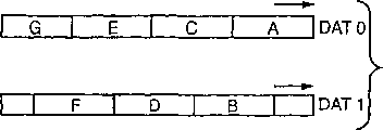
A second aspect of the present invention sees that Fig. 7 to shown in Figure 12, has wherein introduced the Data Transmission Feature of New type of S D card.By increasing the data line (transmitting data simultaneously) that each memory card socket connects, improved the speed of data transmission between main frame and each card via these lines.In this example, shown four data lines, this makes message transmission rate increase to four times.Between main frame and mmc card, only transmit data via one in many data lines.In the specific embodiment of SD card, nonrecoverable data line or one, or four.
The socket 100 of SD card 90 and cooperation with it as shown in Figure 7.Though a first aspect of the present invention of introducing with reference to figure 4 to Fig. 6 above, can utilize with Fig. 1 in the card of mmc card 10 number of contacts as much realize that this aspect of the present invention makes the number increase of the electric contact of SD card.SD card 90 has and the identical contact 11-17 of mmc card 10 among Fig. 1, and at same relative position, but also has two the new contacts 91 and 92 that increase for data transmission.The spare contact 11 of mmc card also is used for data transmission by the SD card now.Therefore, the SD card uses 11,17,91 and 92 4 contacts, the storer within the data transmission access card 90.A kind of socket 100 (see figure 7)s of cooperation have the stitch 1-7 identical with socket 20 among Fig. 1 equally, add two additional stitch 8 and 9.As a result, each memory card socket is connecting 27 (stitch 7), 101 (stitch 8), 102 (stitch 9) and four data lines of 21 (stitch 1).
The system of revising as shown in Figure 8, wherein main frame 51 " through revising, enable via more than a data line, to 104,106 and more than 108 socket (they have the structure of socket 100 respectively, see Fig. 7) in each, transmit data simultaneously.21,27,101 and 102 4 data lines couple together each socket and multiplex adapter 105 by switching logic circuit 110,111,112 and 113.For a card that inserts in one of socket 106 to 108, to deposit the single data stream in the card in the line 107 in,, in 110 to 113 4 switching logic circuit, alternately switch by the time order by multiplex adapter, with in the response line 109 from the control signal of console controller 52 '.Equally, from card, during reading of data, between circuit 110 to 113, switch, in line 107, be assembled into a kind of so single data stream by multiplex adapter 105.
Each bar in many data lines that memory card socket connects, all be equipped with a switch connecting circuit one of (110 to 113), circuit 110 is used for data line DAT 0, and circuit 111 is used for data line DAT 1, circuit 112 is used for data line DAT 2, and circuit 113 is used for data line DAT 3.They are by the signal controlling on the line 114 that is connected to console controller 52 '.For 104,106 and more than 108 socket in storage card among any one, during write operation, each in the switching logic circuit 110 to 113 all is connected to its four all output its input.Therefore, the data that write just are broadcast to all sockets.But, during from a card reading of data, each in the circuit 110 to 113 all switches to the output line that only input link is connected to the socket connection of having inserted the storage card that reads.
In a specific example, in order to adapt to many data lines, the modification of mode shown in Fig. 9 and Figure 10 A to Figure 10 E has been carried out in data register 35 among Fig. 2 and operation thereof in the SD card.During writing, console controller 52 ' (see figure 8) produces single data stream in line 107.This data stream shown in Figure 10 A, each expression one digit number certificate of wherein alphabetical A, B, C or the like.In order only to transmit the one digit number certificate, multiplex adapter 105 is connected to line 107 to logical circuit 110 to 113 successively one at a time.Have four data contacts thereby DAT 0, DAT 1, DAT 2 and DAT 3 all four situations that data line all uses for storage card, shown in Figure 10 B.Multiplex adapter 105 sends first A via data line DAT 0, send second B via data line DAT 1, send the 3rd C, send the 4th D via DAT 3 via data line DAT 2, restart then numerical digit E is sent to data line DAT 0, the rest may be inferred.Data register 35 ' receives this four data stream, and is reassembled into the data sequence among Figure 10 A, is sent to the data buffer concurrently by circuit 38 ' then, and it is similar to the buffer zone 36 among Fig. 2.Under the preferable case, every independent serial data stream all sends via its data line separately, and this data stream is to be accumulated as piece by its numerical digit, every cyclic redundancy check (" CRC ") position that comprises that all the data computation by this piece goes out.In a specific example, each piece all comprises start bit, is data then, then is CRC, is position of rest then.
Though the message transmission rate of any data line all is limited, transmits data simultaneously via many data lines, the multiple that this speed is improved is approximately equal to the number of data line.For example, if use two data lines, just in line 107, provide data stream shown in Figure 10 C, that have Figure 10 A one half rate.Then, multiplex adapter 105 switches this data stream between data line DAT 0 and DAT 1, produces the data stream shown in Figure 10 D.Then, the data register 35 ' in the card that is addressed is reassembled into data stream among Figure 10 C to DAT 0 and 1 two data stream of DAT, and transmits data concurrently via line 38 '.Iff using a data line, multiplex adapter 105 just is connected such as DAT 0 maintenance with single data line, in the line 107, have the data stream of reduction data rate (shown in Figure 10 E), be directed to this data line.
On the contrary, during from the storage card reading of data, be loaded in the register 35 ' data parallel, and send with the form shown in Figure 10 B, Figure 10 D or Figure 10 E, depend on the number of the data line of use via data line.If via sending data more than a data line, multiplex adapter 105 just switches back and forth,, depend on the number of the data line of use so that in line 107, produce data stream corresponding to one of Figure 10 A, Figure 10 C or Figure 10 E between employed data line.
System among Fig. 8 needs to accept to have the storage card of the data line contact of different numbers, one, two or any other number, the number of the data line that in system, provides (being four data lines in this example), and can in system, freely use and exchange this type of storage card with.For some application, do not need the high data rate that many data lines (being four in this example) provide in the system.Use for these, have a kind of SD cassette tape of version that less data pins is arranged.Correspondingly also reduce the number of interface circuit in this card, thereby reduced the cost of this card.The card that has two activation data pins is also useful, as the card that only has a stitch.
In order in same system, can to use the different card of data line number, under the preferable case, in each card, provide a read-only zones, main frame reads just can determine that it can use how many bar data lines and this cartoon letters behind this zone.In a certain embodiments, it is included in the SD card configuration register (" SCR "), and this register is to increase in the register of mmc card shown in Figure 2.When inserting a neocaine when powering up, during certain At All Other Times initialization or in the socket, main frame 51 " all to read this zone, the number of the data line that can adapt to every card transmits the data that are addressed subsequently.But because data line of every increase all can increase some cost because of additional circuit is provided, some card is designed to utilize less data line work.On the contrary, main frame can be designed as, and under the situation that is less than possible data line, also can move.No matter be,, so just can avoid increasing complicacy and cost because higher message transmission rate is provided if, do not need to increase data rate for a kind of concrete application for storage card or for host computer system.
Dynamically select the ability of data-bus width between main frame and one or more storage card, make this main frame can make the message transmission rate between no matter any storage card in it and the insertion system reach maximum.Though might use other technology decomposition data between many data lines fully, but more be ready to use the technology shown in above introduction and Figure 10 A to Figure 10 E, adjust main frame and adapt to the different storage card of data-bus width, when replacing or increase storage card, dynamically adjust, even by using the data line respectively block maximum number, this each of the multiple card different with highway width is opened and is communicated.Another kind of technology is along every data line, alternately sends the packet that comprises a plurality of continuous datas position.Need some overhead but do like this, be used to keep tasks such as tracking data bag.As mentioned above, by each one of many parallel data routings, the continuous numerical digit in the alternate data stream is simpler, especially need adjust to when adapting to the different storage card of data line number when system.Really, except the memory card system that this paper introduces, this data transmission technology also has other application.
Flowchart text among Figure 11 an aspect of the method for operating of accumulator system among Fig. 7 to Figure 10 E, in this system, for every card installing in two or more sockets 104,106 and 108, main frame 51 " guarantee that this card operates required data line number.In first step 121, main frame according to the relative address of RCA register 42 (see figure 2)s that write storage card, carries out addressing to one of storage card via command line 22.Next step, in step 123, main frame reads the data line number of this card from the SCR register of storage card.Then, shown in step 125, this number is with form by host stores under the preferable case.If all storage cards in the socket of system all read, this process finishes; Otherwise step 129 is just to the capable addressing of another Zhang Kajin in the system, and to this card repeating step 123 and 125.
Figure 12 is a process flow diagram, and main frame 51 has been described " storage data of storing card data line number in the using system how.No matter when, as long as main frame carries out addressing to certain memory card socket, shown in step 131, main frame all will the inside form that process makes up from Figure 11 in, read the data line number of this card.This step is shown in step 133.Then, shown in step 135, main frame operation multiplex adapter 105 according to the number that reads, transmits data via DAT 0, DAT 1, DAT 2 and 3 four data lines of DAT from this form.In next procedure 137, transmit data via the data line of this number, no matter go to or from storage card.Have only at storage card under the situation of a data line, in a specific example, main frame transmits data via line 27 (DAT 0) with storage card under the preferable case, because this has adopted the card contact 17 identical with the MMC product, therefore makes system and mmc card compatibility.Mmc card can the same system that is used for Fig. 8 to Figure 10 E with the SD card.Under the preferable case, main frame only sticks into row communication via DAT 0 line and every during initialization, so that determine that this card is mmc card or SD card, if the SD card, also will determine the data line number of its use and the out of Memory of relevant this card, this information makes system improve operational efficiency.
The system of Fig. 8 can either use single command line 22 (not shown)s according to the design of MMC, can use many command connection system of introducing with reference to figure 4 to Fig. 6 again.This selection does not influence the structure and the circuit of storage card.
Though at the specific embodiment in the literary composition, by the agency of many aspects of the present invention, should be appreciated that the present invention has the right to protect the four corner of subsidiary claims.Especially the invention is not restricted to have the system of the data line and the storage card of any concrete number, the number that uses in the introduction of front is only selected for use for illustrative purposes.
Claims (30)
1. an operation comprises the method for the system of a main frame and a plurality of sockets, and in this system, electronic circuit cards can mechanically insert and can be electrically connected at these sockets, and this method comprises:
Transmit data at main frame with between via the card that is connected the command circuit addressing between main frame and a plurality of socket, the data circuit of process also was connected between main frame and a plurality of socket when described data were transmitted, and
Unless the unique address of each card via otherwise once only connect in a plurality of sockets one command circuit and by main frame each only with a card between carry out communicate by letter define in, under normal circumstances, via the command circuit that is connected between main frame and a plurality of socket, transmit the order of control electronic circuit cards operation to single card from main frame.
2. according to the method for claim 1, further comprise:
At least within some electronic circuit cards, store many data contact, can transmit data concurrently by these contacts,
Make main frame from each card that inserts a plurality of sockets, read many data contact of storage, and
It is characterized in that, main frame and be addressed certain open between the card and transmit data, comprising: according to many data contact of storage in the card that is addressed, via one or more transmission data in each many data lines that connecting in main frame and a plurality of socket.
3. according to the method for claim 2, it is characterized in that regardless of the line that the card that inserts in the socket is transmitted simultaneously data how many bars being arranged, main frame all provides a kind of clock signal with public clock frequency to a plurality of sockets, so that the electronic circuit cards that operation is wherein inserted.
4. according to the method for any one claim among the claim 1-3, it is characterized in that electronic circuit cards comprises rewritable nonvolatile memory, wherein storing the data that transmit.
5. an operation comprises the method for the system of a main frame and at least one socket, and in this system, at least one in a plurality of electronic circuit cards removably inserted these sockets at every turn, forms with the contact that utilizes card to be electrically connected, and this method comprises:
Within each electronic circuit cards, store many data contact, can transmit data concurrently by these contacts,
Make main frame from inserting described at least one Zhang Kazhong of described at least one socket, read many data contact of storage, and
Many data contact of storing in the card according to described at least one insertion via one or more in the many lines that connecting main frame and described at least one socket, transmit data between the card of main frame and described at least one insertion.
6. according to the method for claim 5, it is characterized in that no matter transmit the line of data simultaneously how many bars being arranged, main frame all provides a kind of clock signal with public clock frequency to described at least one socket, so that operate the card of described at least one insertion.
7. according to the method for any one claim in claim 5 and 6, it is characterized in that electronic circuit cards comprises rewritable nonvolatile memory, wherein storing the data that transmit.
8. according to the method for claim 7, it is characterized in that main frame determines that the card of a described insertion is the multimedia card type, if just only transmit data via one in many data lines that lead to described at least one socket.
9. according to the method for claim 7, it is characterized in that, between the card of main frame and described at least one insertion, transmit data, comprise many described data line, guide each numerical digit in the serial data stream successively by many data contact of storing in the card corresponding to a described insertion.
10. accumulator system comprises:
(A) memory card of many encapsulation comprises respectively:
A controller of a programmable nonvolatile memory and this storer,
A plurality of electric contacts on outside surface of this card, at least one of these contacts are loaded with and go to and from the data of storer, only reception in these contacts is used to control the order of controller and storage operation and sends response, one of them contact receives the clock signal that is used for operation control and storer, and
A plurality of registers can be programmed by the command signal that receives by the command contact, and can be read by the response signal that sends by the command contact, comprise a programmable address register,
(B) a plurality of sockets, they accept one of many cards respectively, and described socket comprises respectively:
At least one first stitch is in the position of the above at least one data contact of card that connection wherein inserts, and first stitch of each socket is connected at least one public data line together,
One second stitch, the above has only the position of a command contact to be in card that connection wherein inserts, and second stitch of each socket is connected to other command line of branch,
One the 3rd stitch is in the position of the above clock signal contact of card that connection wherein inserts, and the 3rd stitch of a plurality of sockets is connected to public clock cable together, and
(C) main process equipment, be connected on described at least one common data line and transmit and receive data, tranmitting data register signal on the common clock signal line, unless and when having confirmed unique address in the address register of many cards by one of each bar command line at every turn, under normal circumstances, all, receive response signal via each all bar command lines to described independent card transmit operation order with from this clamping simultaneously by comprising an address of certain independent card.
11. accumulator system according to claim 10, it is characterized in that, described at least one common data line comprises two or more data line, memory card provides the response of expression number of contacts respectively, these contacts are loaded with the data of going to and going up storer from this card, insert this response of the card of a plurality of sockets, can read via the command line by main frame, described main frame be connected to a plurality of sockets in each in one or more two of determining via the number of responses that reads from each card by main frame of each memory card of inserting or the more data line transmit data.
12. according to the accumulator system of claim 11, no matter with two of transmitting that data pass through of each memory card or the number of multidata line more, the clock signal on the common clock signal line all has the frequency that remains unchanged.
13. an accumulator system comprises:
Many cards have a plurality of external contact respectively, and these contacts comprise: at least one contact, data are sent out and are conveyed into the rewritable nonvolatile memory in the card; Only a contact receives the response signal that order sends from storer with operational store and response by it; And a contact, the clock signal of reception operational store,
A plurality of sockets, described card inserts respectively wherein, the contact of card and the electric contact of a plurality of corresponding stitch, stitch comprises at least one data pins, a stitch and clock signal stitch that is used for order and response signal only,
A kind of host computer system; Has the single line that is loaded with the command and response signal; Can be connected to by Selection of chiller the command and response signal pins of any one or full socket in each card socket; Described host computer system also has at least one line in addition; Be connected in a plurality of sockets described at least one data pins of each; To be loaded with to and from the data of the card of insertion wherein; Described host computer system also comprises a clock cable; Be connected in a plurality of sockets the described clock signal stitch of each
Described many cards comprise an address register respectively, and main frame is by the order and the response stitch of the card socket of the single card of insertion, and by the order and the response line that are connected to single card at every turn, the address of confirming this card therein is unique, and
By address stored in the address register that on order and response line, sends a described independent card, when described order and response line are connected to the order of all a plurality of sockets and respond stitch, described main frame is by this line, send additional order to an independent card, and absorb the response signal that adds from this clamping.
14. an accumulator system comprises:
Many cards, have a plurality of external contact respectively, wherein one or more contacts are sent out data and be conveyed into the rewritable nonvolatile memory in the card, a contact receives the signal that order sends from storer with operational store and response, and the clock signal of a contact reception operational store
A plurality of sockets, described card inserts respectively wherein, the contact of card and the electric contact of a plurality of corresponding stitch, stitch comprises two or more data pins, a stitch and a stitch that is used for clock signal that is used for order and response signal,
A kind of host computer system, between the order and response stitch of it and a plurality of sockets, a line with the order of being loaded with and response signal; Has a line that is loaded with constant frequency clock signal, via a line that is connected to the described clock signal stitch of each in a plurality of sockets; And two or more overloading the line of data is arranged, be connected in a plurality of sockets two or more data pins of each,
Described many cards are being stored the indication information of the number of the contact that can transmit data simultaneously respectively, and the indication information of described storage can be read via order and response line by main frame, and
According to the indication information of storage in each card, described main frame transmits data to each card that inserts in a plurality of sockets.
15. the accumulator system according to claim 14 is characterized in that, this host computer system comprises the single line that is loaded with order and response signal, can be selected to be connected in each card socket the order and the response signal stitch of any one or full socket by main frame; Described many cards comprise an address register respectively, and main frame is by the order and the response stitch of the card socket of the single card of insertion, and by the order and the response line that are connected to single card at every turn, the address of confirming this card therein is unique; And by address stored in the address register that on order and response line, sends a described independent card, when described order and response line are connected to the order of all a plurality of sockets and respond stitch, described main frame is by this line, send additional order to an independent card, and absorb the response signal that adds from this clamping.
16. a closed card comprises rewritable nonvolatile memory, it has a plurality of contacts, and these a plurality of contacts comprise: one or more contacts of first group, between storer and external host, transmit data simultaneously by this contact; One or more contacts of second group receive the order of operational store from external host, and send the signal of storage operation state to external host; One or more contacts of the 3rd group, the clock signal of reception memorizer operation; A register area, the indication information of first group of interior number of contacts of permanent storage; And an interface circuit, be connected to indication information according to storage, by the number of first group of contact, write data from memory read data with to storer.
17. the card according to claim 16 is characterized in that, card is 32 millimeters long, 24 mm wides, and 1.4 millimeters or 2.1 millimeters thick.
18. a closed card comprises rewritable nonvolatile memory, it has a plurality of contacts, and these a plurality of contacts comprise one or more contacts of first group, transmit data simultaneously by this contact between storer and external host; One or more contacts of second group receive the order of operational store from external host, and send the signal of storage operation state to external host; One or more contacts of the 3rd group, the clock signal of reception memorizer operation; A register area, an address of storing this card, main frame can read this address by first group contact; And a randomizer, the card address is write described register area.
19. a method that transmits serial data stream between first and second equipment comprises:
Can be used for carrying out concurrently of data bit communication from described equipment and to a plurality of lines, determine the number of data line between first and second equipment,
At every turn after one described number of first and second equipment one or more have passed to another generation of described first and second equipment, be in switch data stream between the line of described number of described first and second equipment, and
After each described number one or more have been received generation, by between the data line of described number, switching, locate to re-assembly serial data stream at another of described first and second equipment.
20. the method according to claim 19 is characterized in that, the number of described data line is stored among of described first and second equipment, and its feature also is, the number of the data line of storage is read by another of described first and second equipment.
21. the method according to any one claim in claim 19 or 20 is characterized in that, one or more numbers is a data bit.
22. a memory card comprises:
A shell,
The rewritable nonvolatile memory that this shell is interior,
A plurality of electronic contacts on this shell outside, that be electrically connected with wherein described storer, comprise one group of contact forming by one or more contacts, transmit data or transmit data to described storer simultaneously by this group contact from described storer, by at least one contact order is sent to described storer, receive the clock signal that described storer uses by another contact at least, and
The device that comprises the electronic circuit in the shell, be used at least one by one group of data contact, provide one about transmitting data and when described storer transmits data to described storer simultaneously by one group of data contact, the indication of the number of data contact in described this group data contact.
23. the memory card according to claim 22 also comprises:
Comprise in the shell, response is used for providing the device of interface circuit of indicating device electronic circuit of number of described group data contact data contact, the contact that is used for the indicated number of the described contact sets of process writes data from described memory read data or to described storer, through described contact sets, transmit data and transmit data to described storer simultaneously from described storer.
24. memory card according to claim 22, wherein the indicating device electronic circuit comprises a register area, be used for storing indication,, transmit data and transmit data to described storer simultaneously from described storer through described contact sets about data contact number in the described contact sets.
25. an operation comprises the method for the system of main frame and at least one socket, in this system, described socket is used for removably holding electronic circuit cards and is electrically connected to form between the external contact of main frame and circuit card, and this method comprises:
The circuit card that will comprise rewritable nonvolatile memory is inserted in described at least one socket,
After this, the communication between the circuit card of initializes host and insertion comprises by main frame and addresses inquires to card, and with the number of one or more contacts of determining circuit card, data transmit by these contacts, and
After this, the number by determined one or more circuit card contact transmits data between the rewritable nonvolatile memory in main frame and circuit card, and data transmit by these contacts.
26. according to the method for claim 25, wherein, address inquires to card by main frame and comprise the register that reads in the card, to determine the number of one or more circuit card contact, data transmit through these contacts.
27. according to the method for claim 26, wherein main frame reads register by one of card contact, data transmit through these card contacts.
28. according to the method for claim 27, wherein data transmit the number of card contact of process can be one of described card contact, also can be the number that comprises two or more cards contact of one of described card contact.
29. according to the method for claim 25, wherein the main frame specified data is only to transmit with circuit card through one of circuit card contact.
30. according to the method for claim 25, wherein the main frame specified data transmits with circuit card through two or more circuit card contact.
Applications Claiming Priority (2)
| Application Number | Priority Date | Filing Date | Title |
|---|---|---|---|
| US09/641,023 US6820148B1 (en) | 2000-08-17 | 2000-08-17 | Multiple removable non-volatile memory cards serially communicating with a host |
| US09/641,023 | 2000-08-17 |
Publications (2)
| Publication Number | Publication Date |
|---|---|
| CN1455897A CN1455897A (en) | 2003-11-12 |
| CN1208735C true CN1208735C (en) | 2005-06-29 |
Family
ID=24570622
Family Applications (1)
| Application Number | Title | Priority Date | Filing Date |
|---|---|---|---|
| CNB018155804A Expired - Lifetime CN1208735C (en) | 2000-08-17 | 2001-08-14 | Multiple removable non-volatile memory cards serially communicating with host |
Country Status (11)
| Country | Link |
|---|---|
| US (10) | US6820148B1 (en) |
| EP (13) | EP2312449B1 (en) |
| JP (3) | JP5048203B2 (en) |
| KR (1) | KR100932892B1 (en) |
| CN (1) | CN1208735C (en) |
| AT (1) | ATE386294T1 (en) |
| AU (1) | AU2001286495A1 (en) |
| DE (2) | DE1309919T1 (en) |
| HK (1) | HK1057935A1 (en) |
| TW (1) | TW561346B (en) |
| WO (1) | WO2002015020A2 (en) |
Families Citing this family (128)
| Publication number | Priority date | Publication date | Assignee | Title |
|---|---|---|---|---|
| WO1996024138A1 (en) | 1995-01-31 | 1996-08-08 | Hitachi, Ltd. | Nonvolatile memory device and refreshing method |
| US7295443B2 (en) | 2000-07-06 | 2007-11-13 | Onspec Electronic, Inc. | Smartconnect universal flash media card adapters |
| US6438638B1 (en) * | 2000-07-06 | 2002-08-20 | Onspec Electronic, Inc. | Flashtoaster for reading several types of flash-memory cards with or without a PC |
| US6820148B1 (en) * | 2000-08-17 | 2004-11-16 | Sandisk Corporation | Multiple removable non-volatile memory cards serially communicating with a host |
| US7107378B1 (en) | 2000-09-01 | 2006-09-12 | Sandisk Corporation | Cooperative interconnection and operation of a non-volatile memory card and an input-output card |
| AU2002232494A1 (en) * | 2000-12-07 | 2002-06-18 | Sandisk Corporation | System, method, and device for playing back recorded audio, video or other content from non-volatile memory cards, compact disks or other media |
| US7275112B1 (en) * | 2001-08-08 | 2007-09-25 | Pasternak Solutions Llc | Efficient serialization of bursty out-of-order results |
| JP3552213B2 (en) * | 2001-08-31 | 2004-08-11 | 株式会社東芝 | SD memory card host controller and clock control method |
| JP4082913B2 (en) * | 2002-02-07 | 2008-04-30 | 株式会社ルネサステクノロジ | Memory system |
| US7092256B1 (en) | 2002-04-26 | 2006-08-15 | Sandisk Corporation | Retractable card adapter |
| US7367503B2 (en) | 2002-11-13 | 2008-05-06 | Sandisk Corporation | Universal non-volatile memory card used with various different standard cards containing a memory controller |
| US20050055479A1 (en) * | 2002-11-21 | 2005-03-10 | Aviad Zer | Multi-module circuit card with inter-module direct memory access |
| US8037229B2 (en) * | 2002-11-21 | 2011-10-11 | Sandisk Technologies Inc. | Combination non-volatile memory and input-output card with direct memory access |
| FI20022113A (en) * | 2002-11-29 | 2004-08-06 | Nokia Corp | Method and system for detecting bus width, electronic device and peripheral unit |
| TW556910U (en) * | 2002-12-30 | 2003-10-01 | Carry Computer Eng Co Ltd | Reading device of card reader using SATA (Serial Advanced Technology Attachment) |
| DE112004000140T5 (en) | 2003-01-13 | 2006-02-09 | Rambus Inc., Los Altos | Coded writing mask |
| US6826663B2 (en) | 2003-01-13 | 2004-11-30 | Rambus Inc. | Coded write masking |
| US7305535B2 (en) | 2003-04-17 | 2007-12-04 | Sandisk Corporation | Memory cards including a standard security function |
| FI20035072A0 (en) * | 2003-05-22 | 2003-05-22 | Nokia Corp | Interface bus, electronic device and system |
| US6973519B1 (en) * | 2003-06-03 | 2005-12-06 | Lexar Media, Inc. | Card identification compatibility |
| KR100475125B1 (en) * | 2003-06-21 | 2005-03-14 | 삼성전자주식회사 | Movable storage apparatus capable of freely changing width of data bus and method for setting width of data bus of the same |
| US7036054B2 (en) * | 2003-07-02 | 2006-04-25 | Nokia Corporation | Memory bus checking procedure |
| KR100577392B1 (en) | 2003-08-29 | 2006-05-10 | 삼성전자주식회사 | Method for Enhancing Transfer Rate of Multi-Media-Card Using Differential Signal |
| US7209995B2 (en) * | 2003-12-09 | 2007-04-24 | Sandisk Corporation | Efficient connection between modules of removable electronic circuit cards |
| JP4515793B2 (en) * | 2004-03-11 | 2010-08-04 | 株式会社東芝 | Memory card device and memory card control method |
| TWI227500B (en) * | 2004-03-12 | 2005-02-01 | Winbond Electronics Corp | Operating method of read function of memory card having automatic adaptive function and card controller |
| US7152801B2 (en) * | 2004-04-16 | 2006-12-26 | Sandisk Corporation | Memory cards having two standard sets of contacts |
| US7487265B2 (en) * | 2004-04-16 | 2009-02-03 | Sandisk Corporation | Memory card with two standard sets of contacts and a hinged contact covering mechanism |
| US7269669B2 (en) * | 2004-07-07 | 2007-09-11 | Sychip Inc | Sharing single host controller with multiple functional devices |
| US7814377B2 (en) * | 2004-07-09 | 2010-10-12 | Sandisk Corporation | Non-volatile memory system with self test capability |
| KR100677127B1 (en) * | 2004-07-28 | 2007-02-02 | 삼성전자주식회사 | Method and apparatus for automatically switching memory card in multi-functional device |
| US7427027B2 (en) * | 2004-07-28 | 2008-09-23 | Sandisk Corporation | Optimized non-volatile storage systems |
| EP1811395A4 (en) * | 2004-09-28 | 2008-01-02 | Zentek Technology Japan Inc | Host controller |
| US7657687B2 (en) * | 2004-10-01 | 2010-02-02 | Panasonic Corporation | Memory card controller, memory card drive device, and computer program |
| WO2006057049A1 (en) | 2004-11-26 | 2006-06-01 | Kabushiki Kaisha Toshiba | Card and host device |
| JP4817836B2 (en) | 2004-12-27 | 2011-11-16 | 株式会社東芝 | Card and host equipment |
| JP4892852B2 (en) * | 2005-03-29 | 2012-03-07 | 富士通セミコンダクター株式会社 | Serial interface control method |
| JP2007011753A (en) * | 2005-06-30 | 2007-01-18 | Toshiba Corp | Information processing system and its control method |
| JP4896450B2 (en) * | 2005-06-30 | 2012-03-14 | 株式会社東芝 | Storage device |
| US7710736B2 (en) | 2005-08-02 | 2010-05-04 | Sandisk Corporation | Memory card with latching mechanism for hinged cover |
| JP2009508247A (en) * | 2005-09-14 | 2009-02-26 | コーニンクレッカ フィリップス エレクトロニクス エヌ ヴィ | Method and system for bus arbitration |
| DE102005045149A1 (en) * | 2005-09-22 | 2007-04-05 | Giesecke & Devrient Gmbh | Method for initializing and / or personalizing a portable data carrier |
| US8661540B2 (en) | 2005-10-07 | 2014-02-25 | Imation Corp. | Method and apparatus for secure credential entry without physical entry |
| US7640424B2 (en) * | 2005-10-13 | 2009-12-29 | Sandisk Corporation | Initialization of flash storage via an embedded controller |
| US20070145135A1 (en) * | 2005-12-28 | 2007-06-28 | Fabrice Jogand-Coulomb | Methods used in a nested memory system with near field communications capability |
| US20070145152A1 (en) * | 2005-12-28 | 2007-06-28 | Fabrice Jogand-Coulomb | Nested memory system with near field communications capability |
| US7739487B2 (en) * | 2006-01-17 | 2010-06-15 | Nokia Corporation | Method for booting a host device from an MMC/SD device, a host device bootable from an MMC/SD device and an MMC/SD device method a host device may booted from |
| CN101166034B (en) * | 2006-06-13 | 2012-10-10 | 中宇科技有限公司 | Frequency playing device capable of inserting card and inserting card identification method |
| US20080016312A1 (en) * | 2006-07-12 | 2008-01-17 | Tyler Thorp | Method for Managing Data on Removable Storage Devices in an Electronic Library |
| US8661185B2 (en) * | 2006-07-12 | 2014-02-25 | Sandisk Technologies Inc. | Electronic library for managing data on removable storage devices |
| US7696044B2 (en) * | 2006-09-19 | 2010-04-13 | Sandisk Corporation | Method of making an array of non-volatile memory cells with floating gates formed of spacers in substrate trenches |
| US7646054B2 (en) * | 2006-09-19 | 2010-01-12 | Sandisk Corporation | Array of non-volatile memory cells with floating gates formed of spacers in substrate trenches |
| US8327454B2 (en) * | 2006-11-14 | 2012-12-04 | Sandisk Technologies Inc. | Method for allowing multiple users to access preview content |
| US8763110B2 (en) | 2006-11-14 | 2014-06-24 | Sandisk Technologies Inc. | Apparatuses for binding content to a separate memory device |
| US8079071B2 (en) * | 2006-11-14 | 2011-12-13 | SanDisk Technologies, Inc. | Methods for accessing content based on a session ticket |
| US7800161B2 (en) * | 2006-12-21 | 2010-09-21 | Sandisk Corporation | Flash NAND memory cell array with charge storage elements positioned in trenches |
| US7642160B2 (en) * | 2006-12-21 | 2010-01-05 | Sandisk Corporation | Method of forming a flash NAND memory cell array with charge storage elements positioned in trenches |
| KR100882207B1 (en) * | 2007-04-04 | 2009-02-06 | 삼성전자주식회사 | Memory card including connector for other memory card independently interfacing host using MMC protocol |
| US8762640B2 (en) | 2007-06-27 | 2014-06-24 | Sandisk Il Ltd. | Method for operating a memory interface with SIM functions |
| JP4473900B2 (en) * | 2007-08-22 | 2010-06-02 | 株式会社東芝 | Semiconductor memory device |
| WO2009027802A1 (en) * | 2007-08-28 | 2009-03-05 | Nokia Corporation | Method for bus testing and addressing in mass memory components |
| JP2009054103A (en) * | 2007-08-29 | 2009-03-12 | Panasonic Corp | Host apparatus for controlling multiple memory cards |
| US7774511B2 (en) * | 2007-10-11 | 2010-08-10 | Sandisk Il Ltd. | Addressing multiple devices on a shared bus |
| JP5124237B2 (en) * | 2007-11-02 | 2013-01-23 | 株式会社日立製作所 | Storage system and storage subsystem |
| KR101412524B1 (en) | 2008-01-31 | 2014-06-25 | 삼성전자주식회사 | Memory card system and identification method thereof |
| JP5166922B2 (en) * | 2008-03-10 | 2013-03-21 | キヤノン株式会社 | Shared bus control device and control method thereof |
| US20100017558A1 (en) * | 2008-04-11 | 2010-01-21 | Richard Matthew Fruin | Memory device operable in read-only and re-writable modes of operation |
| US8862821B2 (en) * | 2008-07-08 | 2014-10-14 | Sandisk Il Ltd. | Portable device for managing memory cards |
| US8161219B2 (en) * | 2008-09-30 | 2012-04-17 | Qimonda Ag | Distributed command and address bus architecture for a memory module having portions of bus lines separately disposed |
| JPWO2010047059A1 (en) * | 2008-10-24 | 2012-03-22 | パナソニック株式会社 | Card host LSI and set device having the same |
| US8472199B2 (en) * | 2008-11-13 | 2013-06-25 | Mosaid Technologies Incorporated | System including a plurality of encapsulated semiconductor chips |
| JP5269625B2 (en) * | 2009-01-14 | 2013-08-21 | 株式会社東芝 | Interface control device |
| EP2389645B1 (en) | 2009-01-21 | 2014-09-03 | Imation Corp. | Removable memory storage device with multiple authentication processes |
| US20100205355A1 (en) * | 2009-02-11 | 2010-08-12 | Memory Experts International Inc. | Multiplexing secure digital memory |
| US8566508B2 (en) * | 2009-04-08 | 2013-10-22 | Google Inc. | RAID configuration in a flash memory data storage device |
| KR101606880B1 (en) * | 2009-06-22 | 2016-03-28 | 삼성전자주식회사 | Data storage system and channel driving method thereof |
| US8516232B2 (en) * | 2009-06-30 | 2013-08-20 | Sandisk Technologies Inc. | Method and memory device for performing an operation on data |
| US8392614B2 (en) | 2009-07-27 | 2013-03-05 | Sandisk Il Ltd. | Device identifier selection |
| US8312088B2 (en) * | 2009-07-27 | 2012-11-13 | Sandisk Il Ltd. | Device identifier selection |
| WO2011018677A1 (en) | 2009-08-14 | 2011-02-17 | Sandisk Il Ltd. | Dual interface card with backward and forward compatibility |
| US8775825B2 (en) | 2009-08-17 | 2014-07-08 | Cram Worldwide Llc | Digital content management and delivery |
| JP5150591B2 (en) | 2009-09-24 | 2013-02-20 | 株式会社東芝 | Semiconductor device and host device |
| US8255655B2 (en) | 2009-10-02 | 2012-08-28 | Sandisk Technologies Inc. | Authentication and securing of write-once, read-many (WORM) memory devices |
| USD628202S1 (en) | 2009-10-20 | 2010-11-30 | Sandisk Corporation | MicroSD memory card with different color surfaces |
| US8690283B2 (en) | 2009-10-20 | 2014-04-08 | Sandisk Il Ltd. | Method and system for printing graphical content onto a plurality of memory devices and for providing a visually distinguishable memory device |
| USD638431S1 (en) | 2009-10-20 | 2011-05-24 | Sandisk Corporation | MicroSD memory card with a semi-transparent color surface |
| KR101476112B1 (en) | 2009-12-17 | 2014-12-23 | 가부시끼가이샤 도시바 | Host controller and semiconduct0r device |
| JP2011159267A (en) * | 2010-02-03 | 2011-08-18 | Agile Patch Solutions Inc | Memory system with a plurality of replaceable nonvolatile memories |
| US7888966B1 (en) | 2010-03-25 | 2011-02-15 | Sandisk Corporation | Enhancement of input/output for non source-synchronous interfaces |
| US8085099B2 (en) | 2010-04-06 | 2011-12-27 | Sandisk Technologies Inc. | Self-calibrating relaxation oscillator based clock source |
| KR20110116710A (en) * | 2010-04-20 | 2011-10-26 | 삼성전자주식회사 | Apparatus and method for supporting a plurality of exterior memory in portable terminal |
| US20120066453A1 (en) * | 2010-09-10 | 2012-03-15 | Action Star Enterprise Co., Ltd. | Card-reading device for multi cards |
| JP5728292B2 (en) * | 2011-02-04 | 2015-06-03 | 株式会社東芝 | Memory device and host system |
| US9633391B2 (en) | 2011-03-30 | 2017-04-25 | Cram Worldwide, Llc | Secure pre-loaded drive management at kiosk |
| CN102736859A (en) * | 2011-04-08 | 2012-10-17 | 深圳富泰宏精密工业有限公司 | Double storage card control system and method |
| US8819484B2 (en) | 2011-10-07 | 2014-08-26 | International Business Machines Corporation | Dynamically reconfiguring a primary processor identity within a multi-processor socket server |
| USD667830S1 (en) * | 2011-11-29 | 2012-09-25 | Samsung Electronics Co., Ltd. | SD memory card |
| US20130151755A1 (en) | 2011-12-12 | 2013-06-13 | Reuven Elhamias | Non-Volatile Storage Systems with Go To Sleep Adaption |
| JP5790532B2 (en) * | 2012-02-13 | 2015-10-07 | セイコーエプソン株式会社 | Electronic device and memory control method |
| US9135478B2 (en) * | 2012-03-06 | 2015-09-15 | Iall-Tech Llc | Smartcard and computer quick connect and release system |
| KR20140027859A (en) | 2012-08-27 | 2014-03-07 | 삼성전자주식회사 | Host device and system including the same |
| US8904078B2 (en) | 2012-10-22 | 2014-12-02 | Lenovo Enterprise Solutions (Singapore) Pte. Ltd. | High speed serial peripheral interface system |
| US9647997B2 (en) | 2013-03-13 | 2017-05-09 | Nagrastar, Llc | USB interface for performing transport I/O |
| USD759022S1 (en) | 2013-03-13 | 2016-06-14 | Nagrastar Llc | Smart card interface |
| USD729808S1 (en) | 2013-03-13 | 2015-05-19 | Nagrastar Llc | Smart card interface |
| USD758372S1 (en) * | 2013-03-13 | 2016-06-07 | Nagrastar Llc | Smart card interface |
| US9888283B2 (en) | 2013-03-13 | 2018-02-06 | Nagrastar Llc | Systems and methods for performing transport I/O |
| US9411721B2 (en) | 2013-11-15 | 2016-08-09 | Sandisk Technologies Llc | Detecting access sequences for data compression on non-volatile memory devices |
| US10114787B2 (en) * | 2014-02-03 | 2018-10-30 | Qualcomm Incorporated | Device identification generation in electronic devices to allow external control of device identification for bus communications identification, and related systems and methods |
| US9177654B2 (en) | 2014-03-26 | 2015-11-03 | Burst Corporation | Solid-state memory device with plurality of memory cards |
| USD736213S1 (en) * | 2014-07-01 | 2015-08-11 | Samsung Electronics Co., Ltd. | Memory card |
| KR102285789B1 (en) | 2014-07-01 | 2021-08-04 | 삼성전자 주식회사 | An external storage device, and a method of setting up a reference frequency of the same |
| USD736212S1 (en) * | 2014-07-01 | 2015-08-11 | Samsung Electronics Co., Ltd. | Memory card |
| USD736216S1 (en) * | 2014-07-30 | 2015-08-11 | Samsung Electronics Co., Ltd. | Memory card |
| USD739856S1 (en) * | 2014-07-30 | 2015-09-29 | Samsung Electronics Co., Ltd. | Memory card |
| USD780763S1 (en) | 2015-03-20 | 2017-03-07 | Nagrastar Llc | Smart card interface |
| US20160292400A1 (en) * | 2015-03-30 | 2016-10-06 | Honeywell International Inc. | Sd card license mechanism |
| USD864968S1 (en) | 2015-04-30 | 2019-10-29 | Echostar Technologies L.L.C. | Smart card interface |
| US10013389B2 (en) | 2015-06-09 | 2018-07-03 | Avago Technologies General Ip (Singapore) Pte. Ltd. | Automatic cascaded address selection |
| US10127172B2 (en) * | 2015-06-22 | 2018-11-13 | Qualcomm Technologies International, Ltd. | Single SDIO interface with multiple SDIO units |
| DE102015113491A1 (en) * | 2015-08-14 | 2017-02-16 | Ebm-Papst Mulfingen Gmbh & Co. Kg | dynamic addressing |
| USD783622S1 (en) * | 2015-08-25 | 2017-04-11 | Samsung Electronics Co., Ltd. | Memory card |
| USD783621S1 (en) * | 2015-08-25 | 2017-04-11 | Samsung Electronics Co., Ltd. | Memory card |
| KR102528557B1 (en) | 2016-01-12 | 2023-05-04 | 삼성전자주식회사 | Operating Method of semiconductor device and memory system having multi-connection port and Communication Method of storage system |
| JP6512134B2 (en) * | 2016-02-26 | 2019-05-15 | 株式会社デンソー | Data processing apparatus and data processing system |
| US10235312B2 (en) | 2016-10-07 | 2019-03-19 | Samsung Electronics Co., Ltd. | Memory system and host device that maintain compatibility with memory devices under previous standards and/or versions of standards |
| CN107977233B (en) * | 2016-10-19 | 2021-06-01 | 华为技术有限公司 | Method and device for quickly loading kernel mirror image file |
| KR102511948B1 (en) * | 2019-05-31 | 2023-03-22 | 애플 인크. | High capacity computer modules |
Family Cites Families (62)
| Publication number | Priority date | Publication date | Assignee | Title |
|---|---|---|---|---|
| US467064A (en) * | 1892-01-12 | Trousers | ||
| JPS6086642A (en) | 1983-10-18 | 1985-05-16 | Fujitsu Ltd | Setting system of memory control information |
| JPS6095649A (en) | 1983-10-28 | 1985-05-29 | Fujitsu Ltd | Memory card assigning system |
| US4660141A (en) * | 1983-12-06 | 1987-04-21 | Tri Sigma Corporation | Self configuring computer network with automatic bus exchange of module identification numbers and processor assigned module numbers |
| US4674064A (en) * | 1984-08-06 | 1987-06-16 | General Electric Company | Selectable bit length serial-to-parallel converter |
| US4773005A (en) * | 1984-09-07 | 1988-09-20 | Tektronix, Inc. | Dynamic address assignment system |
| US4656620A (en) | 1984-09-19 | 1987-04-07 | Itt Corporation | Apparatus for obtaining reduced pin count packaging and methods |
| US4918598A (en) | 1985-08-14 | 1990-04-17 | Apple Computer, Inc. | Method for selectively activating and deactivating devices having same first address and different extended addresses |
| US4910655A (en) | 1985-08-14 | 1990-03-20 | Apple Computer, Inc. | Apparatus for transferring signals and data under the control of a host computer |
| US4730251A (en) | 1985-10-28 | 1988-03-08 | International Business Machines Corporation | Automatic I/O address assignment |
| US5038320A (en) | 1987-03-13 | 1991-08-06 | International Business Machines Corp. | Computer system with automatic initialization of pluggable option cards |
| JP2579170B2 (en) * | 1987-09-18 | 1997-02-05 | 日立マクセル株式会社 | Memory card |
| JPH02178869A (en) | 1988-12-29 | 1990-07-11 | Yokogawa Electric Corp | Recognition processing method for package input/output card |
| JPH02222030A (en) | 1989-02-23 | 1990-09-04 | Toshiba Corp | Personal computer |
| JP2862177B2 (en) | 1989-07-19 | 1999-02-24 | 株式会社東芝 | IC card and IC card control method |
| CA1338639C (en) | 1989-09-26 | 1996-10-08 | Seiichi Kubo | Communication control device |
| JPH03216776A (en) * | 1990-01-22 | 1991-09-24 | Mitsubishi Electric Corp | Integrated circuit device and microprocessor consisting of this circuit device |
| US5012408A (en) * | 1990-03-15 | 1991-04-30 | Digital Equipment Corporation | Memory array addressing system for computer systems with multiple memory arrays |
| JP2547654B2 (en) * | 1990-06-29 | 1996-10-23 | 三洋電機株式会社 | Data processing device |
| US5357621A (en) * | 1990-09-04 | 1994-10-18 | Hewlett-Packard Company | Serial architecture for memory module control |
| JPH056326A (en) * | 1991-06-27 | 1993-01-14 | Fujitsu Ltd | Terminal address setting system |
| JPH0567028A (en) | 1991-09-06 | 1993-03-19 | Toshiba Corp | Information processor |
| JP3231832B2 (en) * | 1991-11-26 | 2001-11-26 | 株式会社日立製作所 | Semiconductor disk using flash memory as storage medium |
| TW261687B (en) | 1991-11-26 | 1995-11-01 | Hitachi Seisakusyo Kk | |
| JP3310011B2 (en) | 1992-03-30 | 2002-07-29 | 株式会社東芝 | Semiconductor memory and semiconductor memory board using the same |
| JPH06195524A (en) * | 1992-09-14 | 1994-07-15 | Toshiba Corp | Memory card device |
| US5590374A (en) * | 1993-09-10 | 1996-12-31 | Fujitsu Limited | Method and apparatus for employing a dummy read command to automatically assign a unique memory address to an interface card |
| US5696993A (en) * | 1993-12-03 | 1997-12-09 | Intel Corporation | Apparatus for decoding and providing the decoded addresses to industry standard PCMCIA card through the data lines of the parallel port |
| WO1995034086A1 (en) | 1994-06-03 | 1995-12-14 | Motorola Inc. | A dual function interface for pcmcia compatible peripheral cards and method of use therein |
| US5572683A (en) * | 1994-06-15 | 1996-11-05 | Intel Corporation | Firmware selectable address location and size for cis byte and ability to choose between common memory mode and audio mode by using two external pins |
| JPH086892A (en) | 1994-06-24 | 1996-01-12 | Toshiba Corp | Storage element connecting method and bus control unit |
| JP3548252B2 (en) * | 1994-12-13 | 2004-07-28 | キヤノン株式会社 | External memory address control device and address control method |
| JPH08221222A (en) * | 1995-02-16 | 1996-08-30 | Hitachi Ltd | Information processor |
| US5636342A (en) * | 1995-02-17 | 1997-06-03 | Dell Usa, L.P. | Systems and method for assigning unique addresses to agents on a system management bus |
| US5659741A (en) | 1995-03-29 | 1997-08-19 | Stuart S. Bowie | Computer system and method for storing medical histories using a carrying size card |
| JPH08305814A (en) * | 1995-04-27 | 1996-11-22 | Mitsubishi Electric Corp | Pc card |
| US5696928A (en) | 1995-05-22 | 1997-12-09 | Lucent Technologies | Memory chip architecture for digital storage of prerecorded audio data wherein each of the memory cells are individually addressable |
| DE19614238C1 (en) | 1996-04-10 | 1997-12-11 | Siemens Ag | Communication system with a master station and at least one slave station |
| US5761732A (en) * | 1996-06-28 | 1998-06-02 | Intel Corporation | Interleaving for memory cards |
| US5854891A (en) | 1996-08-09 | 1998-12-29 | Tritheim Technologies, Inc. | Smart card reader having multiple data enabling storage compartments |
| JPH10302030A (en) * | 1997-02-28 | 1998-11-13 | Toshiba Corp | Connection device and information processor |
| DE19713240C2 (en) | 1997-03-29 | 1999-01-28 | Endress Hauser Gmbh Co | Procedure for automatic address assignment in a CAN network |
| US5953515A (en) * | 1997-04-11 | 1999-09-14 | International Business Machines Corporation | Pluggable electronic card presence detect scheme for use in parallel and serial vital detect product data (VPD) collection systems |
| US6128681A (en) * | 1997-08-07 | 2000-10-03 | Avid Technology, Inc. | Serial to parallel and parallel to serial, converter for a digital audio workstation |
| US6304930B1 (en) * | 1998-01-20 | 2001-10-16 | Matsushita Electric Industrial Co., Ltd. | Signal transmission system having multiple transmission modes |
| US6233640B1 (en) * | 1999-03-19 | 2001-05-15 | In-System Design, Inc. | Universal serial bus peripheral bridge with sequencer |
| US6101499A (en) * | 1998-04-08 | 2000-08-08 | Microsoft Corporation | Method and computer program product for automatically generating an internet protocol (IP) address |
| US6040622A (en) | 1998-06-11 | 2000-03-21 | Sandisk Corporation | Semiconductor package using terminals formed on a conductive layer of a circuit board |
| US6166653A (en) * | 1998-08-13 | 2000-12-26 | Motorola Inc | System for address initialization of generic nodes in a distributed command and control system and method therefor |
| CA2347230C (en) * | 1998-10-23 | 2005-12-20 | Octave Communications, Inc. | Serial-to-parallel/parallel-to-serial conversion engine |
| US6240478B1 (en) | 1998-10-30 | 2001-05-29 | Eaton Corporation | Apparatus and method for addressing electronic modules |
| US6279114B1 (en) | 1998-11-04 | 2001-08-21 | Sandisk Corporation | Voltage negotiation in a single host multiple cards system |
| US6901457B1 (en) | 1998-11-04 | 2005-05-31 | Sandisk Corporation | Multiple mode communications system |
| JP2000207137A (en) * | 1999-01-12 | 2000-07-28 | Kowa Co | Information storage device |
| US6634561B1 (en) * | 1999-06-24 | 2003-10-21 | Sandisk Corporation | Memory card electrical contact structure |
| US6438625B1 (en) * | 1999-10-21 | 2002-08-20 | Centigram Communications Corporation | System and method for automatically identifying slots in a backplane |
| US6587942B1 (en) * | 2000-01-03 | 2003-07-01 | Oak Technology, Inc. | Circuit for converting input serial data in a plurality of possible formats into output data in parallel format by interpreting input data format indication information |
| JP3815936B2 (en) | 2000-01-25 | 2006-08-30 | 株式会社ルネサステクノロジ | IC card |
| JP4649009B2 (en) * | 2000-03-08 | 2011-03-09 | 株式会社東芝 | Information processing apparatus having a card interface, card-type electronic equipment that can be mounted on the apparatus, and operation mode setting method in the apparatus |
| US6438638B1 (en) * | 2000-07-06 | 2002-08-20 | Onspec Electronic, Inc. | Flashtoaster for reading several types of flash-memory cards with or without a PC |
| US6820148B1 (en) * | 2000-08-17 | 2004-11-16 | Sandisk Corporation | Multiple removable non-volatile memory cards serially communicating with a host |
| KR100577392B1 (en) * | 2003-08-29 | 2006-05-10 | 삼성전자주식회사 | Method for Enhancing Transfer Rate of Multi-Media-Card Using Differential Signal |
-
2000
- 2000-08-17 US US09/641,023 patent/US6820148B1/en not_active Expired - Lifetime
-
2001
- 2001-08-14 EP EP10075594.1A patent/EP2312449B1/en not_active Expired - Lifetime
- 2001-08-14 CN CNB018155804A patent/CN1208735C/en not_active Expired - Lifetime
- 2001-08-14 EP EP10075647A patent/EP2306326A1/en not_active Ceased
- 2001-08-14 AU AU2001286495A patent/AU2001286495A1/en not_active Abandoned
- 2001-08-14 AT AT01965945T patent/ATE386294T1/en not_active IP Right Cessation
- 2001-08-14 EP EP10075592.5A patent/EP2278475B1/en not_active Expired - Lifetime
- 2001-08-14 DE DE1309919T patent/DE1309919T1/en active Pending
- 2001-08-14 WO PCT/US2001/025550 patent/WO2002015020A2/en active Search and Examination
- 2001-08-14 EP EP10075595A patent/EP2278477A3/en not_active Withdrawn
- 2001-08-14 EP EP10075593A patent/EP2278476B1/en not_active Expired - Lifetime
- 2001-08-14 DE DE60132780T patent/DE60132780T2/en not_active Expired - Lifetime
- 2001-08-14 EP EP10075599A patent/EP2278481B1/en not_active Expired - Lifetime
- 2001-08-14 EP EP10075648A patent/EP2278483A3/en not_active Withdrawn
- 2001-08-14 EP EP01965945A patent/EP1309919B1/en not_active Expired - Lifetime
- 2001-08-14 EP EP10075646.9A patent/EP2278482B1/en not_active Expired - Lifetime
- 2001-08-14 EP EP10075597.4A patent/EP2278479B1/en not_active Expired - Lifetime
- 2001-08-14 EP EP10075598.2A patent/EP2278480B1/en not_active Expired - Lifetime
- 2001-08-14 EP EP07024071A patent/EP1903448B1/en not_active Expired - Lifetime
- 2001-08-14 JP JP2002520082A patent/JP5048203B2/en not_active Expired - Fee Related
- 2001-08-14 KR KR1020037002335A patent/KR100932892B1/en not_active IP Right Cessation
- 2001-08-14 EP EP10075596.6A patent/EP2278478B1/en not_active Expired - Lifetime
- 2001-08-16 TW TW090120103A patent/TW561346B/en not_active IP Right Cessation
-
2004
- 2004-02-06 HK HK04100772A patent/HK1057935A1/en not_active IP Right Cessation
- 2004-05-19 US US10/849,748 patent/US6948016B2/en not_active Expired - Lifetime
- 2004-05-19 US US10/850,309 patent/US6941403B2/en not_active Expired - Lifetime
-
2005
- 2005-08-16 US US11/205,342 patent/US7177964B2/en not_active Expired - Lifetime
-
2007
- 2007-02-12 US US11/673,958 patent/US7305505B2/en not_active Expired - Lifetime
- 2007-11-29 US US11/947,131 patent/US7590782B2/en not_active Expired - Fee Related
-
2009
- 2009-06-03 US US12/477,341 patent/US7895377B2/en not_active Expired - Fee Related
-
2010
- 2010-04-16 US US12/762,041 patent/US8015340B2/en not_active Expired - Fee Related
-
2011
- 2011-01-18 US US13/008,813 patent/US8386678B2/en not_active Expired - Fee Related
- 2011-12-02 JP JP2011264249A patent/JP5200155B2/en not_active Expired - Fee Related
-
2012
- 2012-05-09 JP JP2012107209A patent/JP2012168979A/en active Pending
-
2013
- 2013-01-16 US US13/743,072 patent/US8700833B2/en not_active Expired - Fee Related
Also Published As
Similar Documents
| Publication | Publication Date | Title |
|---|---|---|
| CN1208735C (en) | Multiple removable non-volatile memory cards serially communicating with host | |
| US11016672B2 (en) | Memory card and host device thereof |
Legal Events
| Date | Code | Title | Description |
|---|---|---|---|
| C06 | Publication | ||
| PB01 | Publication | ||
| C14 | Grant of patent or utility model | ||
| GR01 | Patent grant | ||
| C41 | Transfer of patent application or patent right or utility model | ||
| TR01 | Transfer of patent right |
Effective date of registration: 20160525 Address after: texas Patentee after: Sandisk Corp. Address before: American California Patentee before: Sandisk Corp. |
|
| C56 | Change in the name or address of the patentee | ||
| CP01 | Change in the name or title of a patent holder |
Address after: texas Patentee after: DELPHI INT OPERATIONS LUX SRL Address before: texas Patentee before: Sandisk Corp. |
|
| CX01 | Expiry of patent term | ||
| CX01 | Expiry of patent term |
Granted publication date: 20050629 |