CN116107101A - Diffraction device based on cholesteric liquid crystal - Google Patents
Diffraction device based on cholesteric liquid crystal Download PDFInfo
- Publication number
- CN116107101A CN116107101A CN202310093172.7A CN202310093172A CN116107101A CN 116107101 A CN116107101 A CN 116107101A CN 202310093172 A CN202310093172 A CN 202310093172A CN 116107101 A CN116107101 A CN 116107101A
- Authority
- CN
- China
- Prior art keywords
- light
- clc
- layer
- liquid crystal
- waveguide
- Prior art date
- Legal status (The legal status is an assumption and is not a legal conclusion. Google has not performed a legal analysis and makes no representation as to the accuracy of the status listed.)
- Pending
Links
Images


Classifications
-
- G—PHYSICS
- G02—OPTICS
- G02F—OPTICAL DEVICES OR ARRANGEMENTS FOR THE CONTROL OF LIGHT BY MODIFICATION OF THE OPTICAL PROPERTIES OF THE MEDIA OF THE ELEMENTS INVOLVED THEREIN; NON-LINEAR OPTICS; FREQUENCY-CHANGING OF LIGHT; OPTICAL LOGIC ELEMENTS; OPTICAL ANALOGUE/DIGITAL CONVERTERS
- G02F1/00—Devices or arrangements for the control of the intensity, colour, phase, polarisation or direction of light arriving from an independent light source, e.g. switching, gating or modulating; Non-linear optics
- G02F1/01—Devices or arrangements for the control of the intensity, colour, phase, polarisation or direction of light arriving from an independent light source, e.g. switching, gating or modulating; Non-linear optics for the control of the intensity, phase, polarisation or colour
- G02F1/13—Devices or arrangements for the control of the intensity, colour, phase, polarisation or direction of light arriving from an independent light source, e.g. switching, gating or modulating; Non-linear optics for the control of the intensity, phase, polarisation or colour based on liquid crystals, e.g. single liquid crystal display cells
- G02F1/137—Devices or arrangements for the control of the intensity, colour, phase, polarisation or direction of light arriving from an independent light source, e.g. switching, gating or modulating; Non-linear optics for the control of the intensity, phase, polarisation or colour based on liquid crystals, e.g. single liquid crystal display cells characterised by the electro-optical or magneto-optical effect, e.g. field-induced phase transition, orientation effect, guest-host interaction or dynamic scattering
- G02F1/13718—Devices or arrangements for the control of the intensity, colour, phase, polarisation or direction of light arriving from an independent light source, e.g. switching, gating or modulating; Non-linear optics for the control of the intensity, phase, polarisation or colour based on liquid crystals, e.g. single liquid crystal display cells characterised by the electro-optical or magneto-optical effect, e.g. field-induced phase transition, orientation effect, guest-host interaction or dynamic scattering based on a change of the texture state of a cholesteric liquid crystal
-
- G—PHYSICS
- G02—OPTICS
- G02B—OPTICAL ELEMENTS, SYSTEMS OR APPARATUS
- G02B27/00—Optical systems or apparatus not provided for by any of the groups G02B1/00 - G02B26/00, G02B30/00
- G02B27/0093—Optical systems or apparatus not provided for by any of the groups G02B1/00 - G02B26/00, G02B30/00 with means for monitoring data relating to the user, e.g. head-tracking, eye-tracking
-
- G—PHYSICS
- G02—OPTICS
- G02B—OPTICAL ELEMENTS, SYSTEMS OR APPARATUS
- G02B27/00—Optical systems or apparatus not provided for by any of the groups G02B1/00 - G02B26/00, G02B30/00
- G02B27/01—Head-up displays
- G02B27/017—Head mounted
- G02B27/0172—Head mounted characterised by optical features
-
- G—PHYSICS
- G02—OPTICS
- G02F—OPTICAL DEVICES OR ARRANGEMENTS FOR THE CONTROL OF LIGHT BY MODIFICATION OF THE OPTICAL PROPERTIES OF THE MEDIA OF THE ELEMENTS INVOLVED THEREIN; NON-LINEAR OPTICS; FREQUENCY-CHANGING OF LIGHT; OPTICAL LOGIC ELEMENTS; OPTICAL ANALOGUE/DIGITAL CONVERTERS
- G02F1/00—Devices or arrangements for the control of the intensity, colour, phase, polarisation or direction of light arriving from an independent light source, e.g. switching, gating or modulating; Non-linear optics
- G02F1/01—Devices or arrangements for the control of the intensity, colour, phase, polarisation or direction of light arriving from an independent light source, e.g. switching, gating or modulating; Non-linear optics for the control of the intensity, phase, polarisation or colour
- G02F1/011—Devices or arrangements for the control of the intensity, colour, phase, polarisation or direction of light arriving from an independent light source, e.g. switching, gating or modulating; Non-linear optics for the control of the intensity, phase, polarisation or colour in optical waveguides, not otherwise provided for in this subclass
-
- G—PHYSICS
- G02—OPTICS
- G02F—OPTICAL DEVICES OR ARRANGEMENTS FOR THE CONTROL OF LIGHT BY MODIFICATION OF THE OPTICAL PROPERTIES OF THE MEDIA OF THE ELEMENTS INVOLVED THEREIN; NON-LINEAR OPTICS; FREQUENCY-CHANGING OF LIGHT; OPTICAL LOGIC ELEMENTS; OPTICAL ANALOGUE/DIGITAL CONVERTERS
- G02F1/00—Devices or arrangements for the control of the intensity, colour, phase, polarisation or direction of light arriving from an independent light source, e.g. switching, gating or modulating; Non-linear optics
- G02F1/01—Devices or arrangements for the control of the intensity, colour, phase, polarisation or direction of light arriving from an independent light source, e.g. switching, gating or modulating; Non-linear optics for the control of the intensity, phase, polarisation or colour
- G02F1/13—Devices or arrangements for the control of the intensity, colour, phase, polarisation or direction of light arriving from an independent light source, e.g. switching, gating or modulating; Non-linear optics for the control of the intensity, phase, polarisation or colour based on liquid crystals, e.g. single liquid crystal display cells
- G02F1/133—Constructional arrangements; Operation of liquid crystal cells; Circuit arrangements
- G02F1/1333—Constructional arrangements; Manufacturing methods
- G02F1/1335—Structural association of cells with optical devices, e.g. polarisers or reflectors
- G02F1/133504—Diffusing, scattering, diffracting elements
-
- G—PHYSICS
- G02—OPTICS
- G02F—OPTICAL DEVICES OR ARRANGEMENTS FOR THE CONTROL OF LIGHT BY MODIFICATION OF THE OPTICAL PROPERTIES OF THE MEDIA OF THE ELEMENTS INVOLVED THEREIN; NON-LINEAR OPTICS; FREQUENCY-CHANGING OF LIGHT; OPTICAL LOGIC ELEMENTS; OPTICAL ANALOGUE/DIGITAL CONVERTERS
- G02F1/00—Devices or arrangements for the control of the intensity, colour, phase, polarisation or direction of light arriving from an independent light source, e.g. switching, gating or modulating; Non-linear optics
- G02F1/29—Devices or arrangements for the control of the intensity, colour, phase, polarisation or direction of light arriving from an independent light source, e.g. switching, gating or modulating; Non-linear optics for the control of the position or the direction of light beams, i.e. deflection
- G02F1/292—Devices or arrangements for the control of the intensity, colour, phase, polarisation or direction of light arriving from an independent light source, e.g. switching, gating or modulating; Non-linear optics for the control of the position or the direction of light beams, i.e. deflection by controlled diffraction or phased-array beam steering
-
- G—PHYSICS
- G06—COMPUTING; CALCULATING OR COUNTING
- G06F—ELECTRIC DIGITAL DATA PROCESSING
- G06F3/00—Input arrangements for transferring data to be processed into a form capable of being handled by the computer; Output arrangements for transferring data from processing unit to output unit, e.g. interface arrangements
- G06F3/01—Input arrangements or combined input and output arrangements for interaction between user and computer
- G06F3/03—Arrangements for converting the position or the displacement of a member into a coded form
- G06F3/033—Pointing devices displaced or positioned by the user, e.g. mice, trackballs, pens or joysticks; Accessories therefor
- G06F3/038—Control and interface arrangements therefor, e.g. drivers or device-embedded control circuitry
-
- G—PHYSICS
- G02—OPTICS
- G02B—OPTICAL ELEMENTS, SYSTEMS OR APPARATUS
- G02B27/00—Optical systems or apparatus not provided for by any of the groups G02B1/00 - G02B26/00, G02B30/00
- G02B27/01—Head-up displays
- G02B27/0101—Head-up displays characterised by optical features
- G02B2027/0132—Head-up displays characterised by optical features comprising binocular systems
- G02B2027/0134—Head-up displays characterised by optical features comprising binocular systems of stereoscopic type
-
- G—PHYSICS
- G02—OPTICS
- G02B—OPTICAL ELEMENTS, SYSTEMS OR APPARATUS
- G02B27/00—Optical systems or apparatus not provided for by any of the groups G02B1/00 - G02B26/00, G02B30/00
- G02B27/01—Head-up displays
- G02B27/0179—Display position adjusting means not related to the information to be displayed
- G02B2027/0185—Displaying image at variable distance
-
- G—PHYSICS
- G02—OPTICS
- G02F—OPTICAL DEVICES OR ARRANGEMENTS FOR THE CONTROL OF LIGHT BY MODIFICATION OF THE OPTICAL PROPERTIES OF THE MEDIA OF THE ELEMENTS INVOLVED THEREIN; NON-LINEAR OPTICS; FREQUENCY-CHANGING OF LIGHT; OPTICAL LOGIC ELEMENTS; OPTICAL ANALOGUE/DIGITAL CONVERTERS
- G02F2201/00—Constructional arrangements not provided for in groups G02F1/00 - G02F7/00
- G02F2201/34—Constructional arrangements not provided for in groups G02F1/00 - G02F7/00 reflector
- G02F2201/343—Constructional arrangements not provided for in groups G02F1/00 - G02F7/00 reflector cholesteric liquid crystal reflector
Landscapes
- Physics & Mathematics (AREA)
- Nonlinear Science (AREA)
- General Physics & Mathematics (AREA)
- Optics & Photonics (AREA)
- Engineering & Computer Science (AREA)
- Chemical & Material Sciences (AREA)
- Crystallography & Structural Chemistry (AREA)
- Theoretical Computer Science (AREA)
- General Engineering & Computer Science (AREA)
- Mathematical Physics (AREA)
- Human Computer Interaction (AREA)
- Liquid Crystal (AREA)
- Diffracting Gratings Or Hologram Optical Elements (AREA)
- Eyeglasses (AREA)
Abstract
The present disclosure relates to a diffraction device based on cholesteric liquid crystals. Examples of diffraction devices include Cholesteric Liquid Crystal (CLC) layers that include a plurality of chiral structures, wherein each chiral structure includes a plurality of liquid crystal molecules that extend at least one pitch in a depth-of-layer direction and rotate continuously in a first rotational direction. The arrangement of the liquid crystal molecules of the chiral structure is periodically varied in a lateral direction perpendicular to the layer depth direction to provide a diffraction grating. The diffraction device may be configured to reflect light having a specific wavelength range and circular polarization sense. Diffraction devices may be used in waveguide and imaging systems in enhanced or virtual systems.
Description
The present application is a divisional application of application having a filing date of 2017, 12 months of 7, PCT international application No. PCT/US2017/065182, chinese national phase application No. 201780085689.4, and the name of "cholesteric liquid crystal based diffraction device".
Cross Reference to Related Applications
The present application claims the benefit of priority from U.S. provisional patent application No. 62/431,752, entitled "DIFFRACTIVE DEVICES BASED ON CHOLESTERIC LIQUID CRYSTAL (cholesteric liquid Crystal based diffraction device)", filed 8 at 12 of 2016, and U.S. provisional patent application No. 62/431,745, entitled "DIFFRACTIVE DEVICES BASED ON CHOLESTERIC LIQUID CRYSTAL (cholesteric liquid Crystal based diffraction device)", filed 8 at 12 of 2016, the entire contents of which are incorporated herein by reference.
Technical Field
The present disclosure relates to display systems, and more particularly, to augmented reality display systems including cholesteric liquid crystal based diffractive devices.
Background
Modern computing and display technologies have facilitated the development of systems for so-called "virtual reality" or "augmented reality" experiences, in which digitally rendered images, or portions thereof, are presented to a user in a manner that appears to be real or may be perceived as real. Virtual reality or "VR" scenes typically involve the presentation of digital or virtual image information while being opaque to other actual real world visual inputs; augmented reality or "AR" scenes generally involve the presentation of digital or virtual image information as an enhancement to the visualization of the real world around the user. Mixed reality or "MR" scenes are "AR" type scenes and generally involve virtual objects that are integrated into and responsive to the natural world. For example, in an MR scene, AR image content may be blocked by or perceived as interacting with objects in the real world.
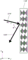
Referring to fig. 1, an augmented reality scene 1 is shown in which a user of AR technology sees a real-world park-like setting 1100 featuring people, trees, buildings in the background, and a concrete platform 1120. In addition to these items, the user of the AR technology also perceives that he/she "sees" virtual content ", such as a robotic figurine 1110 standing on the real world platform 1120, and a flying cartoon avatar character 1130 that appears to be a bumblebee avatar, even if these elements 1130, 1110 are not present in the real world. Because the human visual perception system is complex, it is challenging to produce AR technology that facilitates comfortable, natural-feeling, rich presentation of virtual image elements in addition to other virtual or real world image elements.
The systems and methods disclosed herein address various challenges associated with AR and VR techniques.
Disclosure of Invention
In one aspect, a diffraction grating includes a Cholesteric Liquid Crystal (CLC) layer including a plurality of chiral structures, wherein each chiral structure includes a plurality of liquid crystal molecules that extend at least one pitch in a depth-of-layer direction and continuously rotate in a first rotational direction. The pitch is the length in the depth direction of the layer, which corresponds to the net rotation angle of one complete rotation of the liquid crystal molecules of the chiral structure in the first rotation direction. The arrangement of the liquid crystal molecules of the chiral structure periodically varies in a lateral direction perpendicular to the layer depth direction.
In another aspect, a head mounted display device (HMD) is configured to project light to a user's eye to display augmented reality image content. The HMD includes a head mounted display device including a frame configured to be supported on a head of the user. The HMD includes a display disposed on the frame, wherein at least a portion of the display includes one or more waveguides. The one or more waveguides are transparent and disposed in a position in front of a user's eyes when the user wears the head mounted display device such that the transparent portion transmits light from a portion of a user's front environment to the user's eyes to provide a view of the portion of the user's front environment. The display further includes one or more light sources and at least one diffraction grating configured to couple light from the light sources into or out of the one or more waveguides, wherein the at least one diffraction grating includes a diffraction grating according to aspects described elsewhere herein.
In another aspect, a waveguide device includes one or more Cholesteric Liquid Crystal (CLC) layers, each CLC layer including a plurality of chiral structures, wherein each chiral structure includes a plurality of liquid crystal molecules that extend in a layer depth direction and continuously rotate in a first rotation direction, wherein an arrangement of the liquid crystal molecules of the chiral structures periodically varies in a transverse direction perpendicular to the layer depth direction such that the one or more CLC layers are configured to Bragg-reflect incident light. One or more waveguides are formed over the one or more CLC layers and configured to optically couple bragg reflected light such that the bragg reflected light propagates via Total Internal Reflection (TIR) in a lateral direction perpendicular to the layer depth direction. The one or more CLC layers and the one or more waveguides are configured to be in the same optical path.
In another aspect, a wavelength selective Cholesteric Liquid Crystal Reflector (CLCR) includes one or more Cholesteric Liquid Crystal (CLC) layers, each CLC layer including a plurality of chiral structures, wherein each chiral structure includes a plurality of liquid crystal molecules that extend in a depth-of-layer direction and continuously rotate in a first rotation direction. The arrangement of liquid crystal molecules of the chiral structure varies periodically in a lateral direction perpendicular to the layer depth direction such that the one or more CLC layers are configured to substantially bragg reflect a first incident light having a first wavelength while substantially transmitting a second incident light having a second wavelength.
In another aspect, a Head Mounted Display (HMD) configured to be worn on a user's head includes a frame including a pair of earstems; a pair of optical elements supported by the frame such that each of the pair of optical elements is capable of being disposed in front of an eye of the user; a forward imager mounted to one of the pair of earstems; and a Cholesteric Liquid Crystal (CLC) off-axis mirror (mirror) comprising one or more Cholesteric Liquid Crystal (CLC) layers, each CLC layer comprising a plurality of chiral structures. Each chiral structure comprises a plurality of liquid crystal molecules extending in a layer depth direction and continuously rotating in a first rotation direction, wherein an arrangement of liquid crystal molecules of the chiral structure periodically varies in a lateral direction perpendicular to the layer depth direction such that the one or more CLC layers are configured to bragg reflect incident light. The Cholesteric Liquid Crystal (CLC) off-axis mirror is disposed in or on one of the pair of optical elements and is configured to reflect infrared light toward the forward imager configured to receive infrared light reflected by the reflective element.
In another aspect, a waveguide device includes one or more Cholesteric Liquid Crystal (CLC) layers, each CLC layer including a plurality of chiral structures, wherein each chiral structure includes a plurality of liquid crystal molecules that extend in a layer depth direction and continuously rotate in a first rotation direction, wherein an arrangement of the liquid crystal molecules of the chiral structures periodically varies in a transverse direction perpendicular to the layer depth direction such that the one or more CLC layers are configured to bragg reflect incident light. The waveguide device additionally includes one or more waveguides formed over the one or more CLC layers and configured to optically couple bragg reflected light from the one or more CLC layers such that the bragg reflected light propagates in a lateral direction perpendicular to the layer depth direction via Total Internal Reflection (TIR). The waveguide device is configured to have a field of view (FOV) within which the diffraction efficiency is greater than 25%, the field of view exceeding 20 °.
In yet another aspect, a display device includes a waveguide and an in-coupling optical element formed on the waveguide. The coupling-in optical element is configured to couple light incident thereon into a first side of the waveguide, wherein the coupling-in optical element and the waveguide are configured such that light coupled into the waveguide propagates in the waveguide along an in-plane direction of the waveguide via Total Internal Reflection (TIR). The display device additionally includes an out-coupling (outcoupling) optical element formed on the waveguide and configured to couple light incident thereon out of the waveguide. The light out-coupling element comprises a Cholesteric Liquid Crystal (CLC) layer comprising a plurality of chiral structures, wherein each chiral structure comprises a plurality of liquid crystal molecules extending in a layer depth direction of the CLC layer and continuously rotating in a first rotation direction, wherein an arrangement of liquid crystal molecules of the chiral structures periodically varies in a lateral direction perpendicular to the layer depth direction such that the one or more CLC layers are configured to bragg reflect light incident thereon from the waveguide to the first side.
The details of one or more implementations of the subject matter described in this specification are set forth in the accompanying drawings and the description below. Other features, aspects, and advantages will become apparent from the description, the drawings, and the claims. Neither the summary of the invention nor the following detailed description is intended to limit or restrict the scope of the inventive subject matter.
Drawings
Fig. 1 illustrates an Augmented Reality (AR) view that a user views through an AR device.
Fig. 2 shows an example of a wearable display system.
Fig. 3 illustrates a conventional display system for simulating a three-dimensional image for a user.
FIG. 4 illustrates aspects of a method of simulating a three-dimensional image using multiple depth planes.
Fig. 5A to 5C show the relationship between the radius of curvature and the focal radius.
Fig. 6 shows an example of a waveguide stack for outputting image information to a user.
Fig. 7 shows an example of an outgoing light beam output by a waveguide.
Fig. 8 shows an example of a stacked waveguide assembly in which each depth plane includes images formed using a plurality of different component colors.
Fig. 9A shows a cross-sectional side view of an example of a set of stacked waveguides, each including an incoupling optical element.
Fig. 9B shows a perspective view of an example of the plurality of stacked waveguides of fig. 9A.
Fig. 9C shows a top plan view of an example of the plurality of stacked waveguides of fig. 9A and 9B.
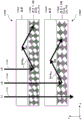
Fig. 10 shows a cross-sectional side view of an example of a cholesteric liquid crystal diffraction grating (CLCG) having a plurality of uniform (unitary) chiral structures.
Fig. 11 shows a cross-sectional side view of an example of a CLCG having differently arranged chiral structures in the lateral direction.
Fig. 12 shows a cross-sectional side view of an example of a CLC layer configured for bragg reflection at an off-axis incident angle.
Fig. 13A shows a cross-sectional side view of an example of a CLC layer having a first pitch and configured to bragg reflect at a first off-axis incident angle.
Fig. 13B shows a cross-sectional side view of an example of a CLC layer having a second pitch and configured to bragg reflect at a second off-axis incident angle.
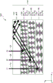
Fig. 13C shows a cross-sectional side view of an example of a CLCG comprising CLC layers of fig. 13A and 13B having different pitches for bragg reflection at multiple off-axis incidence angles and high diffraction bandwidths in a stacked configuration.
Fig. 14 shows a cross-sectional side view of an example of a CLCG including a CLC layer having vertical regions with different pitches in the depth direction for bragg reflection at a plurality of off-axis incident angles and a high diffraction bandwidth.
Fig. 15 shows a cross-sectional side view of an example of a CLCG comprising a CLC layer having lateral regions with a pitch in the lateral direction for spatially varying bragg reflection.
Fig. 16 shows an example of an optical waveguide device including a waveguide coupled to a CLCG and configured to propagate light via Total Internal Reflection (TIR).
Fig. 17A shows an example of an optical waveguide device including a waveguide coupled to a CLCG and configured to selectively propagate light having a wavelength via Total Internal Reflection (TIR).
Fig. 17B shows an example of multiple optical waveguide devices in the same optical path, each optical waveguide device including a waveguide coupled to a CLCG and configured to selectively propagate light having a wavelength via Total Internal Reflection (TIR).
Fig. 17C shows an example of multiple optical waveguide devices in the same optical path, each optical waveguide device including a waveguide coupled to a CLCG and configured to selectively propagate light having a wavelength via Total Internal Reflection (TIR).
Fig. 18 shows an example of an optical waveguide device including a common waveguide coupled to a plurality of CLCGs and configured to selectively propagate light having a plurality of wavelengths via Total Internal Reflection (TIR).
Fig. 19 shows an example of an optical waveguide device including a waveguide coupled to a CLCG and configured to propagate light via Total Internal Reflection (TIR).
Fig. 20 shows an example of an optical waveguide device comprising a waveguide coupled to a CLCG configured to receive incident light and a polarization conversion reflector, the waveguide configured to propagate light reflected from the CLCG bragg via Total Internal Reflection (TIR).
Fig. 21A shows the optical waveguide device of fig. 20, wherein the CLCG is configured to receive incident light that is linearly polarized or unpolarized, and wherein the waveguide is configured to propagate light reflected from the CLCG bragg and light reflected by the reflector via Total Internal Reflection (TIR).
Fig. 21B shows the optical waveguide device of fig. 20, wherein the CLCG is configured to receive incident light polarized into an orthogonal elliptical or circularly polarized beam, and wherein the waveguide is configured to propagate light reflected from the CLCG bragg and light reflected by the reflector via Total Internal Reflection (TIR).
Fig. 22A shows an example of an optical waveguide device in a linearly polarized or unpolarized condition of an incident light beam, the optical waveguide device comprising a plurality of CLC layers coupled to a common waveguide, the CLC layers comprising a first CLC layer comprising a chiral structure having a first rotation direction and a second CLC layer comprising a chiral structure having a second rotation direction opposite to the first rotation direction.
Fig. 22B shows the optical waveguide device of fig. 22A in a situation where the incident light is polarized into orthogonal elliptical or circularly polarized beams.
Fig. 22C shows an example of an optical waveguide device in the case of linear polarization or non-polarization of an incident light beam, the optical waveguide device comprising a plurality of CLC layers coupled to a common waveguide interposed between two CLC layers, the CLC layers comprising a first CLC layer comprising a chiral structure having a first rotation direction and a second CLC layer comprising a chiral structure having a second rotation direction opposite to the first rotation direction.
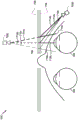
Fig. 23 illustrates an example of an imaging system including a forward-facing camera configured to image a wearer's eye using a Cholesteric Liquid Crystal (CLC) off-axis mirror.
Fig. 24A-24F illustrate examples of an imaging system including a forward-facing camera configured to image a wearer's eye using CLC off-axis mirrors.
24G and 24H illustrate examples of an imaging system including a forward-facing camera configured to image a wearer's eye using a diffractive optical element including a plurality of segments (segments) containing one or more CLC off-axis mirrors, wherein each segment may have different optical characteristics.
Fig. 25 illustrates an example optical waveguide device optimized for a wide field of view, including a waveguide coupled to a CLCG and configured to propagate light via Total Internal Reflection (TIR).
Fig. 26 shows an example optical waveguide device configured as an out-coupling optical element, the optical waveguide device comprising a waveguide coupled to a CLCG and configured to propagate light via Total Internal Reflection (TIR).
Throughout the drawings, reference numerals may be repeated to indicate corresponding relationships between the elements referred to. The drawings are provided to illustrate example embodiments described herein and are not intended to limit the scope of the disclosure.
Detailed Description
The AR system may display virtual content to a user or viewer while still allowing the user to see the world around it. Preferably, the content is displayed on a head mounted display (e.g., as part of glasses) that projects image information to the eyes of the user. In addition, the display may also transmit light from the surrounding environment to the user's eyes to allow viewing of the surrounding environment. As used herein, it should be understood that a "head mounted" display is a display that can be mounted on a viewer's head.
Fig. 2 shows an example of a wearable display system 80. Display system 80 includes display 62, and various mechanical and electronic modules and systems that support the functionality of display 62. The display 62 may be coupled to a frame 64 that may be worn by a display system user or viewer 60 and configured to position the display 62 in front of the eyes of the user 60. In some embodiments, the display 62 may be considered glasses. In some embodiments, a speaker 66 is coupled to the frame 64 and positioned near the ear canal of the user 60 (in some embodiments, another speaker (not shown) is positioned near another ear canal of the user to provide stereo/shapeable sound control). In some embodiments, the display system may also include one or more microphones 67 or other devices to detect sound. In some embodiments, the microphone is configured to allow a user to provide input or commands (e.g., selection of voice menu commands, natural language questions, etc.) to the system 80 and/or may allow audio communication with other people (e.g., with other users of similar display systems). The microphone may also be configured as a peripheral sensor to continuously collect audio data (e.g., to passively collect from the user and/or the environment). Such audio data may include user sounds (such as heavy breathing) or ambient sounds (such as bang indicating nearby events). The display system may also include peripheral sensors 30a, which may be separate from the frame 64 and attached to the body of the user 60 (e.g., on the head, torso, limbs, etc. of the user 60). As further described herein, in some embodiments, peripheral sensor 30a may be configured to acquire data characterizing a physiological state of user 60. For example, the sensor 30a may be an electrode.
With continued reference to fig. 2, the display 62 is operatively coupled to the local data processing module 70 via a communication link 68 (e.g., via a wired lead or wireless connection), and the local data processing module 70 may be mounted in various configurations, such as fixedly attached to the frame 64, fixedly attached to a helmet or hat worn by the user, embedded in the headset, or otherwise removably attached to the user 60 (e.g., in a backpack-type configuration, in a belt-coupled configuration). Similarly, the sensor 30a may be operatively coupled to the local processing and data module 70 by a communication link 30b (e.g., by a wired lead or a wireless connection). The local processing and data module 70 may include a hardware processor, as well as digital memory, such as non-volatile memory (e.g., flash memory or hard drive), both of which may be used to facilitate the processing, caching and storage of data. These data include: a) Data captured from sensors (which may be, for example, operatively coupled to the frame 64 or otherwise attached to the user 60), such as image capture devices (e.g., cameras), microphones, inertial measurement units, accelerometers, compasses, GPS units, radios, gyroscopes, and/or other sensors disclosed herein; and/or b) data acquired and/or processed (including data related to virtual content) using remote processing module 72 and/or remote data repository 74, which may be transferred to display 62 after such processing or retrieval. The local processing and data module 70 may be operatively coupled to the remote processing module 72 and the remote data repository 74 by communication links 76, 78 (such as via wired or wireless communication links) such that these remote modules 72, 74 are operatively coupled to each other and available as resources to the local processing and data module 70. In some embodiments, the local processing and data module 70 may include one or more of an image capture device, a microphone, an inertial measurement unit, an accelerometer, a compass, a GPS unit, a radio, and/or a gyroscope. In some other embodiments, one or more of these sensors may be attached to the frame 64, or may be a stand-alone structure that communicates with the local processing and data module 70 through a wired or wireless communication path.
With continued reference to fig. 2, in some embodiments, the remote processing module 72 may include one or more processors configured to analyze and process data and/or image information. In some embodiments, the remote data repository 74 may include a digital data storage facility that may be obtained through the Internet or other network configuration in a "cloud" resource configuration. In some embodiments, the remote data repository 74 may include one or more remote servers that provide information to the local processing and data module 70 and/or the remote processing module 72, such as information for generating augmented reality content. In some embodiments, all data is stored and all computations are performed in the local processing and data module, allowing full autonomous use from the remote module.
The perception of an image as "three-dimensional" or "3D" may be achieved by providing each eye of the viewer with a slightly different image presentation. Fig. 3 illustrates a conventional display system for simulating a three-dimensional image of a user. Two different images 5, 7 are output to the user, one for each eye 4, 6. The images 5, 7 are separated from the eyes 4, 6 by a distance 10 along an optical or z-axis parallel to the line of sight of the viewer. The images 5, 7 are flat and the eyes 4, 6 can be focused on these images by assuming a single accommodation state. Such a system relies on the human visual system to combine the images 5, 7 to provide a sense of depth and/or zoom to the combined image.
However, it should be appreciated that the human visual system is more complex and that it is more challenging to provide a realistic sensation of depth. For example, many viewers of conventional "3-D" display systems find such systems uncomfortable or not at all perceivable as depth perception. Without being limited by theory, it is believed that a viewer of an object may perceive the object as "three-dimensional" due to a combination of vergence and accommodation. The converging-diverging motion of the two eyes relative to each other (e.g., rotation of the eyes moves the pupils toward or away from each other to converge the line of sight of the eyes to fixate on the subject) is closely related to the focusing (or accommodation) of the lenses and pupils of the eyes. Under normal circumstances, changing the focus of the lens of an eye or adjusting the eye to change focus from one object to another at a different distance will automatically result in a change in vergence matching the same distance, according to a relationship known as "accommodation-vergence" and pupil dilation or constriction. Also, under normal conditions, a change in vergence will trigger a matching accommodation change in lens shape and pupil size. As noted herein, many stereoscopic or "3-D" display systems use slightly different presentations (and, thus, slightly different images) to display a scene to each eye such that the human visual system perceives a three-dimensional perspective. However, such systems are uncomfortable for many viewers because they simply provide different presentations of the scene, in addition to the rest of the content, while the eye views all image information in a single accommodation state and works against "accommodation-vergence reflection". Display systems that provide a better match between accommodation and vergence can create more realistic and comfortable three-dimensional image simulations that help increase wear duration and thus comply with diagnostic and therapeutic protocols.
FIG. 4 illustrates aspects of a method of simulating a three-dimensional image using multiple depth planes. Referring to fig. 4, objects at different distances from the eyes 4, 6 on the z-axis are accommodated by the eyes 4, 6 to bring these objects into focus (in focus). The eyes (4 and 6) present a specific accommodation state to bring objects at different distances along the z-axis into focus. Thus, it can be said that a particular accommodation state is associated with a particular one of the depth planes 14, which has an associated focal length, such that the object or portion of the object in the particular depth plane is in focus when the eye is in the accommodation state for that depth plane. In some embodiments, the three-dimensional image may be simulated by providing each eye 4, 6 with a different presentation of the image, and may also be simulated by providing a different presentation of the image corresponding to each of the depth planes. Although shown separate for clarity of illustration, it should be understood that the fields of view of eyes 4, 6 may overlap as the distance along the z-axis increases, for example. In addition, while shown as flat for ease of illustration, it should be understood that the contour of the depth plane may be curved in physical space such that all features in the depth plane are in focus when the eye is in a particular state of accommodation.
The distance between the object and the eye 4 or 6 may also change the amount of divergence of the light from the object seen by the eye. Fig. 5A to 5C show the relationship between the distance and the light divergence. The distances between the object and the eye 4 are represented by distances R1, R2 and R3 in descending order. As shown in fig. 5A to 5C, as the distance to the object decreases, the light becomes more divergent. As the distance increases, the light becomes more collimated. In other words, it can be said that the light field generated by a point (object or part of an object) has a spherical wavefront curvature, which is a function of the distance of the point from the user's eye. As the distance between the subject and the eye 4 decreases, the curvature increases. Thus, at different depth planes, the divergence of the light rays is also different, the divergence increasing with decreasing distance between the depth plane and the viewer's eye 4. Although only a single eye 4 is shown for clarity of illustration in fig. 5A-5C and other figures herein, it should be understood that the discussion regarding eye 4 may be applied to both eyes 4 and 6 of a viewer.
Without being limited by theory, it is believed that the human eye may generally interpret a limited number of depth planes to provide depth perception. Thus, by providing the eye with a different presentation of the image corresponding to each of these limited number of depth planes, a highly reliable simulation of perceived depth may be achieved. The different presentations may be individually focused by the eyes of the viewer, thereby helping to provide depth cues to the user based on eye accommodation required to bring different image features of a scene located on different depth planes into focus and/or based on observing out-of-focus of different image features on different depth planes.
Fig. 6 shows an example of a waveguide stack for outputting image information to a user. The display system 1000 includes a waveguide stack or stacked waveguide assembly 178 that can be used to provide three-dimensional perception to the eye/brain using a plurality of waveguides 1182, 1184, 1186, 1188, 1190. In some embodiments, the display system 1000 is the system 80 of fig. 2, with fig. 6 schematically showing portions of the system 80 in more detail. For example, the waveguide assembly 1178 may be part of the display 62 of fig. 2. It will be appreciated that in some embodiments, the display system 1000 may be considered a light field display.
With continued reference to fig. 6, the waveguide assembly 1178 may also include a plurality of features 1198, 1196, 1194, 1192 positioned between the waveguides. In some embodiments, the features 1198, 1196, 1194, 1192 may be one or more lenses. The waveguides 1182, 1184, 1186, 1188, 1190 and/or the plurality of lenses 1198, 1196, 1194, 1192 may be configured to transmit image information to the eye with various levels of wavefront curvature or ray divergence. Each waveguide stage may be associated with a particular depth plane and may be configured to output image information corresponding to that depth plane. The image injection devices 1200, 1202, 1204, 1206, 1208 may serve as light sources for the waveguides and may be used to inject image information into the waveguides 1182, 1184, 1186, 1188, 1190, as described herein, each of which may be configured to distribute incident light through each respective waveguide for output toward the eye 4. Light exits the output surfaces 1300, 1302, 1304, 1306, 1308 of the image injection devices 1200, 1202, 1204, 1206, 1208 and is injected into the respective input surfaces 1382, 1384, 1386, 1388, 1390 of the waveguides 1182, 1184, 1186, 1188, 1190. In some embodiments, each of the input surfaces 1382, 1384, 1386, 1388, 1390 may be an edge of a respective waveguide, or may be a portion of a major surface of a respective waveguide (i.e., one of the waveguide surfaces that directly faces the world 1144 or the viewer's eye 4). In some embodiments, a single light beam (e.g., a collimated light beam) may be injected into each waveguide to output the entire field of view of the gram Long Zhunzhi light beam directed toward the eye 4 at a particular angle (and amount of divergence) corresponding to the depth plane associated with the particular waveguide. In some embodiments, one of the image injection devices 1200, 1202, 1204, 1206, 1208 may be associated with a plurality of waveguides 1182, 1184, 1186, 1188, 1190 (e.g., three of them) and inject light into these waveguides.
In some embodiments, the image injection devices 1200, 1202, 1204, 1206, 1208 are discrete displays, each of which generates image information for injection into a corresponding waveguide 1182, 1184, 1186, 1188, 1190, respectively. In some other embodiments, the image injection devices 1200, 1202, 1204, 1206, 1208 are output of a single multiplexed display, e.g., the multiplexed display may pipeline image information to each of the image injection devices 1200, 1202, 1204, 1206, 1208 via one or more optical conduits (e.g., fiber optic cables). It will be appreciated that the image information provided by the image injection devices 1200, 1202, 1204, 1206, 1208 may include light of different wavelengths or colors (e.g., different component colors as discussed herein).
In some embodiments, the light injected into the waveguides 1182, 1184, 1186, 1188, 1190 is provided by a light projector system 2000, the light projector system 2000 comprising a light module 2040, the light module 2040 may comprise a light emitter, such as a Light Emitting Diode (LED). Light from the light module 2040 may be directed to a light modulator 2030 (e.g., a spatial light modulator) via a beam splitter 2050 and modified by the light modulator 2030. The light modulator 2030 may be configured to change the perceived intensity of light injected into the waveguides 1182, 1184, 1186, 1188, 1190. Examples of spatial light modulators include Liquid Crystal Displays (LCDs), which include Liquid Crystal On Silicon (LCOS) displays.
In some embodiments, the display system 1000 may be a scanning fiber display including one or more scanning fibers configured to project light into one or more of the waveguides 1182, 1184, 1186, 1188, 1190 and ultimately into the eye 4 of the viewer in various patterns (e.g., raster scan, spiral scan, lissajous pattern, etc.). In some embodiments, the illustrated image injection devices 1200, 1202, 1204, 1206, 1208 may schematically represent a single scanning fiber or scanning fiber bundle configured to inject light into one or more waveguides 1182, 1184, 1186, 1188, 1190. In some other embodiments, the illustrated image injection devices 1200, 1202, 1204, 1206, 1208 may schematically represent a plurality of scanning fibers or a plurality of scanning fiber bundles, each of which is configured to inject light into an associated one of the waveguides 1182, 1184, 1186, 1188, 1190. It should be appreciated that one or more optical fibers may be configured to transmit light from the optical module 2040 to one or more waveguides 1182, 1184, 1186, 1188, 1190. It should be appreciated that one or more intervening optical structures may be provided between the one or more scanning fibers and the one or more waveguides 1182, 1184, 1186, 1188, 1190, for example, to redirect light exiting the scanning fibers into the one or more waveguides 1182, 1184, 1186, 1188, 1190.
The controller 1210 controls the operation of one or more of the stacked waveguide assemblies 1178, including the operation of the image injection devices 1200, 1202, 1204, 1206, 1208, the light source 2040, and the light modulator 2030. In some embodiments, controller 1210 is part of local data processing module 70. Controller 1210 includes programming (e.g., instructions in a non-transitory medium) that adjusts timing and image information provision to waveguides 1182, 1184, 1186, 1188, 1190 according to, for example, any of the various schemes disclosed herein. In some embodiments, the controller may be a single integrated device or a distributed system connected by a wired or wireless communication channel. In some embodiments, the controller 1210 may be part of the processing module 70 or 72 (fig. 1).
With continued reference to fig. 6, the waveguides 1182, 1184, 1186, 1188, 1190 may be configured to propagate light within each respective waveguide by Total Internal Reflection (TIR). The waveguides 1182, 1184, 1186, 1188, 1190 may each be planar or have another shape (e.g., curved) with top and bottom major surfaces and edges extending between the top and bottom major surfaces. In the illustrated configuration, the waveguides 1182, 1184, 1186, 1188, 1190 may each include an out-coupling (outcoupling) optical element 1282, 1284, 1286, 1288, 1290 configured to extract light from the waveguides by redirecting the light, propagate inside the respective corresponding waveguides, and exit the waveguides to output image information to the eye 4. The extracted light may also be referred to as outcoupled light, while the outcoupled optical element light may also be referred to as light extraction optical element. The light propagating in the waveguide irradiates the position of the light extraction optical element, and the extracted light beam is output by the waveguide. As discussed further herein, the out-coupling optical elements 1282, 1284, 1286, 1288, 1290 may be, for example, gratings, including diffractive optical features. Although shown disposed at the bottom major surface of the waveguides 1182, 1184, 1186, 1188, 1190 for ease of description and clarity of depiction, in some embodiments, the out-coupling optical elements 1282, 1284, 1286, 1288, 1290 may be disposed at the top and/or bottom major surfaces and/or may be disposed directly in the body of the waveguides 1182, 1184, 1186, 1188, 1190, as further discussed herein. In some embodiments, the out-coupling optical elements 1282, 1284, 1286, 1288, 1290 may be formed in a layer of material attached to a transparent substrate to form waveguides 1182, 1184, 1186, 1188, 1190. In some other embodiments, the waveguides 1182, 1184, 1186, 1188, 1190 may be a single piece of material, and the out-coupling optical elements 1282, 1284, 1286, 1288, 1290 may be formed on a surface and/or in an interior of the piece of material.
With continued reference to fig. 6, as discussed herein, each waveguide 1182, 1184, 1186, 1188, 1190 is configured to output light to form an image corresponding to a particular depth plane. For example, the waveguide 1182 closest to the eye may be configured to transmit collimated light injected into such waveguide 1182 to the eye 4. The collimated light may represent an optical infinity focal plane. The next upstream waveguide 1184 may be configured to send out collimated light that passes through the first lens 1192 (e.g., a negative lens) before it can reach the eye 4; such a first lens 1192 may be configured to produce a slightly convex wavefront curvature such that the eye/brain interprets light from the next upstream waveguide 1184 as coming from a first focal plane closer to optical infinity inward toward the eye 4. Similarly, third ascending waveguide 1186 passes its output light through first lens 1192 and second lens 1194 before reaching eye 4; the combined optical power (optical power) of the first lens 1192 and the second lens 1194 may be configured to produce another incremental wavefront curvature such that the eye/brain interprets light from the third waveguide 1186 as coming from a second focal plane that is closer to the inside toward the person from optical infinity than the light from the next upstream waveguide 1184.
The other waveguide layers 1188, 1190 and lenses 1196, 1198 are similarly configured, with the highest waveguide 1190 in the stack sending its output through all lenses between it and the eye to obtain an aggregate power (aggregate focal power) representing the focal plane closest to the person. To compensate for the lens stacks 1198, 1196, 1194, 1192 when viewing/interpreting light from the world 1144 on the other side of the stacked waveguide assembly 1178, a compensating lens layer 1180 may be provided on top of the stacks to compensate for the aggregate power of the underlying lens stacks 1198, 1196, 1194, 1192. This configuration provides as many perceived focal planes as there are waveguide/lens pairs available. Both the out-coupling optics of the waveguide and the focusing aspects of the lens may be static (i.e., not dynamic or electroactive). In some alternative embodiments, one or both of them may be dynamic using electroactive features.
In some embodiments, two or more of the waveguides 1182, 1184, 1186, 1188, 1190 may have the same relevant depth plane. For example, the plurality of waveguides 1182, 1184, 1186, 1188, 1190 may be configured to output the image set to the same depth plane, or the plurality of subsets of waveguides 1182, 1184, 1186, 1188, 1190 may be configured to output the image set to the same plurality of depth planes, one image set per depth plane. This may provide the advantage of forming a tiled image to provide an extended field of view at those depth planes.
With continued reference to fig. 6, the out-coupling optical elements 1282, 1284, 1286, 1288, 1290 may be configured to redirect light out of their respective waveguides and output that light with an appropriate amount of divergence or collimation for a particular depth plane associated with the waveguides. As a result, waveguides having different associated depth planes may have different configurations of out-coupling optical elements 1282, 1284, 1286, 1288, 1290 that output light having different amounts of divergence depending on the associated depth plane. In some embodiments, the light extraction optical elements 1282, 1284, 1286, 1288, 1290 may be body or surface features that may be configured to output light at a particular angle. For example, the light extraction optical elements 1282, 1284, 1286, 1288, 1290 may be volume holograms, surface holograms, and/or diffraction gratings. In some embodiments, the features 1198, 1196, 1194, 1192 may not be lenses; rather, they may simply be spacers (e.g., cladding and/or structures for forming an air gap).
In some embodiments, the out-coupling optical elements 1282, 1284, 1286, 1288, 1290 are diffractive features, or "diffractive optical elements" (also referred to herein as "DOEs") that form a diffractive pattern. Preferably, the DOE has a diffraction efficiency (ratio of diffracted beam intensity to incident beam intensity) that is sufficiently low such that only a portion of the light of the beam is deflected towards the eye 4 by each intersection of the DOE, while the remainder continues to move through the waveguide via total internal reflection. The light carrying the image information is thus split into a plurality of associated outgoing light beams which leave the waveguide at a plurality of positions and as a result are outgoing emissions towards a fairly uniform pattern of the eye 4 for this particular collimated light beam bouncing within the waveguide.
In some embodiments, one or more DOEs may be switchable between an "on" state in which they actively diffract and an "off state in which they do not diffract significantly. For example, the switchable DOE may comprise a polymer dispersed liquid crystal layer in which the droplets contain a diffraction pattern in the host medium, and the refractive index of the droplets may be switched to substantially match the refractive index of the host material (in which case the pattern DOEs not significantly diffract incident light), or the droplets may be switched to a refractive index that DOEs not match the refractive index of the host medium (in which case the pattern actively diffracts incident light).
In some embodiments, a camera assembly 500 (e.g., a digital camera, including visible and infrared light cameras) may be provided to capture images of the eye 4 and/or tissue surrounding the eye 4, for example, to detect user input and/or monitor a physiological state of the user. As used herein, a camera may be any image capturing device. In some embodiments, the camera assembly 500 may include an image capture device and a light source to project light (e.g., infrared light) to the eye, which may then be reflected by the eye and detected by the image capture device. In some embodiments, the camera assembly 500 may be attached to the frame 64 (fig. 2) and may be in electrical communication with the processing modules 70 and/or 72, and the processing modules 70 and/or 72 may process image information from the camera assembly 500 to make various determinations regarding, for example, a physiological state of a user, as described herein. It should be appreciated that information about the physiological state of the user may be used to determine the behavioral or emotional state of the user. Examples of such information include actions of the user and/or facial expressions of the user. The collected environmental and/or virtual content data may then be utilized to triangulate the behavioral or emotional state of the user to determine the relationship between the behavioral or emotional state, the physiological state, and the environmental or virtual content data. In some embodiments, one camera assembly 500 may be used for each eye to monitor each eye separately.
Referring now to fig. 7, an example of an outgoing light beam output by a waveguide is shown. One waveguide is shown, but it should be understood that other waveguides in the waveguide assembly 1178 (fig. 6) may function similarly, with the waveguide assembly 1178 including a plurality of waveguides. Light 400 is injected into waveguide 1182 at input surface 1382 of waveguide 1182 and propagates within waveguide 1182 by TIR. At the point where light 400 impinges on DOE 282, a portion of the light exits the waveguide as exit beam 402. The exit beam 402 is illustrated as being substantially parallel, but as discussed herein, depending on the depth plane associated with the waveguide 1182, the exit beam 402 may also be redirected at an angle (e.g., forming a divergent exit beam) to propagate to the eye 4. It will be appreciated that the substantially parallel outgoing light beam may be indicative of a waveguide having an out-coupling optical element that couples light out to form an image that appears to be disposed on a depth plane at a large distance from the eye 4 (e.g., optical infinity). Other waveguides or other sets of out-coupling optical elements may output a more divergent outgoing beam pattern, which would require the eye 4 to be adjusted to a closer distance to focus it on the retina and would be interpreted by the brain as light from a distance closer to the eye 4 than optical infinity.
In some embodiments, a full color image may be formed at each depth plane by superimposing images in each of the component colors (e.g., three or more component colors). Fig. 8 shows an example of a stacked waveguide assembly in which each depth plane includes images formed using a plurality of different component colors. The illustrated embodiment shows depth planes 14a-14f, but more or less depths are also contemplated. Each depth plane may have three component color images associated with it: a first image of a first color G; a second image of a second color R; and a third image of a third color B. For diopters (dpt) after the letters G, R and B, the different depth planes are indicated by different numbers in the figure. By way of example only, the number following each of these letters represents the diopter (1/m), or the inverse of the distance of the depth plane from the viewer, and each box in the figure represents a separate component color image. In some embodiments, the precise placement of depth planes of different component colors may be varied in order to account for differences in the focus of the eye on different wavelengths of light. For example, different component color images of a given depth plane may be placed on the depth plane corresponding to different distances from the user. Such an arrangement may increase visual acuity and user comfort, and/or may reduce chromatic aberration.
In some embodiments, each component color of light may be output by a single dedicated waveguide, and thus, each depth plane may have multiple waveguides associated with it. In such an embodiment, each box in the figure comprising the letter G, R or B may be understood to represent a separate waveguide, and each depth plane may provide three waveguides, wherein each depth plane provides three component color images. Although the waveguides associated with each depth plane are shown adjacent to each other in this figure for ease of description, it should be understood that in a physical device, the waveguides may all be arranged in a stacked fashion of one waveguide per level. In some other embodiments, multiple component colors may be output by the same waveguide, such that, for example, only a single waveguide may be provided per depth plane.
With continued reference to fig. 8, in some embodiments, G is green, R is red, and B is blue. In some other embodiments, other colors associated with other wavelengths of light (including magenta and cyan) may be used in addition to, or instead of, one or more of red, green, or blue. In some embodiments, features 198, 196, 194, and 192 may be active or passive optical filters configured to block light from the surrounding environment or selectively allow light from the surrounding environment to reach the eyes of the viewer.
It should be understood that reference throughout this disclosure to light of a given color will be understood to include light of one or more wavelengths within a range of wavelengths perceived by a viewer as having that given color of light. For example, red light may include light at one or more wavelengths in the range of about 620-780nm, green light may include light at one or more wavelengths in the range of about 492-577nm, and blue light may include light at one or more wavelengths in the range of about 435-493 nm.
In some embodiments, light source 2040 (fig. 6) may be configured to emit light of one or more wavelengths outside the visual perception range of the viewer, such as infrared and/or ultraviolet wavelengths. Furthermore, the in-coupling, out-coupling and other light redirecting structures of the waveguides of the display 1000 may be configured to direct this light and to direct this light out of the display towards the user's eye 4, for example for imaging and/or user-stimulated applications.
Referring now to fig. 9A, in some embodiments, it may be desirable to redirect light impinging on a waveguide to couple the light into the waveguide. Light may be redirected and coupled into their corresponding waveguides using coupling-in optical elements. Fig. 9A illustrates a cross-sectional side view of an example of a plurality of stacked waveguides or groups of stacked waveguides 1200, each waveguide including an incoupling optical element. The waveguides may each be configured to output light of one or more different wavelengths, or light of one or more different wavelength ranges. It should be appreciated that the stack 1200 may correspond to the stack 1178 (fig. 6), and that the illustrated waveguides of the stack 1200 may correspond to a portion of the plurality of waveguides 1182, 1184, 1186, 1188, 1190, except that light from one or more of the image injection devices 1200, 1202, 1204, 1206, 1208 is injected into the waveguides from a location where light is required to be redirected for coupling in.
The illustrated stacked waveguide set 1200 includes waveguides 1210, 1220, and 1230. Each waveguide includes an associated incoupling optical element (which may also be referred to as an optical input region on the waveguide), where, for example, incoupling optical element 1212 is disposed on a major surface (e.g., a top major surface) of waveguide 1210, incoupling optical element 1224 is disposed on a major surface (e.g., a top major surface) of waveguide 1220, and incoupling optical element 1232 is disposed on a major surface (e.g., a top major surface) of waveguide 1230. In some embodiments, one or more of the incoupling optical elements 1212, 1222, 1232 may be disposed on the bottom major surface of the respective waveguide 1210, 1220, 1230 (particularly where one or more incoupling optical elements are reflective deflecting optical elements). As shown, the incoupling optical elements 1212, 1222, 1232 may be disposed on the top major surface of their respective waveguides 1210, 1220, 1230 (or the top of the next downstream waveguide), particularly in those cases where the incoupling optical elements are transmissive deflecting optical elements. In some embodiments, the incoupling optical elements 1212, 1222, 1232 may be disposed in the body of the respective waveguides 1210, 1220, 1230. In some embodiments, as discussed herein, the incoupling optical elements 1212, 1222, 1232 are wavelength selective such that they selectively redirect light of one or more wavelengths while transmitting light of other wavelengths. Although shown on one side or corner of their respective waveguides 1210, 1220, 1230, it should be understood that in some embodiments, the incoupling optical elements 1212, 1222, 1232 may be disposed in other regions of their respective waveguides 1210, 1220, 1230.
As shown, the incoupling optical elements 1212, 1222, 1232 may be laterally offset from each other. In some embodiments, each in-coupling optical element may be offset such that the in-coupling optical element receives light without the light having to transmit through another in-coupling optical element. For example, as shown in fig. 6, each incoupling optical element 1212, 1222, 1232 may be configured to receive light from a different image injection device 1200, 1202, 1204, 1206, 1208, and may be separate (e.g., laterally spaced) from the other incoupling optical elements 1212, 1222, 1232 such that the incoupling optical element does not substantially receive light from the other incoupling optical elements 1212, 1222, 1232.
Each waveguide also includes an associated light distribution element, wherein, for example, light distribution element 1214 is disposed on a major surface (e.g., a top major surface) of waveguide 1210, light distribution element 1224 is disposed on a major surface (e.g., a top major surface) of waveguide 1220, and light distribution element 1234 is disposed on a major surface (e.g., a top major surface) of waveguide 1230. In some other embodiments, the light distribution elements 1214, 1224, 1234 may be disposed on the bottom major surfaces of the associated waveguides 1210, 1220, 1230, respectively. In some other embodiments, the light distribution elements 1214, 1224, 1234 may be disposed on the top and bottom major surfaces of the associated waveguides 1210, 1220, 1230, respectively; alternatively, the light distribution elements 1214, 1224, 1234 may be disposed on different ones of the top and bottom major surfaces of different associated waveguides 1210, 1220, 1230, respectively.
The waveguides 1210, 1220, 1230 may be separated and separated by, for example, gas, liquid, and/or solid material layers. For example, as shown, layer 1218a may separate waveguides 1210 and 1220; layer 1218b may separate waveguides 1220 and 1230. In some embodiments, layers 1218a and 1218b are formed of a low index material (i.e., a material having a lower index of refraction than the material forming one of the immediately adjacent waveguides 1210, 1220, 1230). Preferably, the refractive index of the material forming the layers 1218a, 1218b is less than the refractive index of the material forming the waveguides 1210, 1220, 1230 by 0.05 or more, or less than 0.10 or more. Advantageously, the lower index layers 1218a, 1218b may act as cladding layers that promote Total Internal Reflection (TIR) of light passing through the waveguides 1210, 1220, 1230 (e.g., TIR between the top and bottom major surfaces of each waveguide). In some embodiments, the layers 1218a, 1218b are formed of air. Although not shown, it should be understood that the top and bottom of the illustrated waveguide stack 1200 may include immediately adjacent cladding layers.
Preferably, the materials forming the waveguides 1210, 1220, 1230 are similar or identical, and the materials forming the layers 1218a, 1218b are similar or identical, for ease of manufacture and for other considerations. In some embodiments, the materials forming waveguides 1210, 1220, 1230 may be different between one or more waveguides, and/or the materials forming layers 1218a, 1218b may be different while still maintaining the various refractive index relationships described above.
With continued reference to fig. 9A, light rays 1240, 1242, 1244 are incident on waveguide group 1200. It should be appreciated that light rays 1240, 1242, 1244 may be injected into waveguides 1210, 1220, 1230 by one or more image injection devices 1200, 1202, 1204, 1206, 1208 (fig. 6).
In some embodiments, light 1240, 1242, 1244 has different characteristics, e.g., different wavelengths or different wavelength ranges, which may correspond to different colors. The incoupling optical elements 1212, 122, 1232 each deflect incident light such that the light propagates through a respective one of the waveguides 1210, 1220, 1230 by TIR.
For example, the in-coupling optical element 1212 may be configured to deflect light 1240 having a first wavelength or first range of wavelengths. Similarly, the transmitted light rays 1242 impinge on the incoupling optical element 1222 and are deflected by the incoupling optical element 1222, which incoupling optical element 1222 is configured to deflect light of a second wavelength or a second wavelength range. Likewise, light rays 1244 are deflected by the incoupling optical element 1232, which incoupling optical element 1232 is configured to selectively deflect light of a third wavelength or third wavelength range.
With continued reference to fig. 9A, the deflected light rays 1240, 1242, 1244 are deflected such that they propagate through the corresponding waveguides 1210, 1220, 1230; that is, the coupling-in optical element 1212, 1222, 1232 of each waveguide deflects light into the corresponding waveguide 1210, 1220, 1230 to couple light into the corresponding waveguide. Light rays 1240, 1242, 1244 are deflected at an angle that causes the light to propagate by TIR through the respective waveguides 1210, 1220, 1230. Light 1240, 1242, 1244 propagates by TIR through the respective waveguide 1210, 1220, 1230 until impinging on the waveguide's corresponding light distribution element 1214, 1224, 1234.
Referring now to fig. 9B, a perspective view of an example of the plurality of stacked waveguides of fig. 9A is shown. As described above, the coupled-in light rays 1240, 1242, 1244 are deflected by the coupling-in optical elements 1212, 1222, 1232, respectively, and then propagate by TIR within the waveguides 1210, 1220, 1230, respectively. Light 1240, 1242, 1244 then impinges on light distribution elements 1214, 1224, 1234, respectively. Light distribution elements 1214, 1224, 1234 deflect light 1240, 1242, 1244 such that light 1240, 1242, 1244 propagates toward coupling-out optical elements 1250, 1252, 1254, respectively.
In some embodiments, the light distribution elements 1214, 1224, 1234 are Orthogonal Pupil Expanders (OPEs). In some embodiments, the OPE both deflects or distributes light to the out- coupling optics 1250, 1252, 1254 and increases the beam or spot size of the light as it propagates to the out-coupling optics. In some embodiments, for example, in embodiments where the beam size is already of a desired size, the light distribution elements 1214, 1224, 1234 may be omitted, and the in-coupling optical elements 1212, 1222, 1232 may be configured to deflect light directly to the out-coupling optical elements 1250, 1252, 1254. For example, referring to fig. 9A, the light distribution elements 1214, 1224, 1234 may be replaced by outcoupling optical elements 1250, 1252, 1254, respectively. In some embodiments, the out-coupling optical elements 1250, 1252, 1254 are an Exit Pupil (EP) or an Exit Pupil Expander (EPE) that directs light into the eye 4 (fig. 7) of the viewer.
Thus, referring to fig. 9A and 9B, in some embodiments, a waveguide group 1200 includes: waveguides 1210, 1220, 1230; coupling into optical elements 1212, 1222, 1232; light distribution elements (e.g., OPEs) 1214, 1224, 1234; and out-coupling optical elements (e.g., EP) 1250, 1252, 1254 for each component color. The waveguides 1210, 1220, 1230 may be stacked with an air gap/cladding between each waveguide. The incoupling optical elements 1212, 1222, 1232 redirect or deflect incident light (where different incoupling optical elements receive light of different wavelengths) into their waveguides. The light then propagates at an angle that will result in TIR within the respective waveguide 1210, 1220, 1230. In the example shown, in the manner previously described, light 1240 (e.g., blue light) is deflected by first incoupling optical element 1212 and then continues to bounce along the waveguide, interacting with light distribution element (e.g., OPE) 1214 and incoupling optical element (e.g., EP) 1250. Light rays 1242 and 1244 (e.g., green and red light, respectively) will be transmitted through the waveguide 1210, with the light rays 1242 impinging on the incoupling optical element 1222 and being deflected by the incoupling optical element 1222. Light ray 1242 then bounces along waveguide 1220 via TIR, proceeds to its light distribution element (e.g., OPE) 1224, and then proceeds to the out-coupling optical element (e.g., EP) 1252. Finally, a light ray 1244 (e.g., red light) is transmitted through the waveguide 1230 to impinge on the light incoupling optical element 1232 of the waveguide 1230. Light incoupling optical element 1232 deflects light rays 1244 such that the light rays propagate by TIR to light distribution element (e.g., OPE) 1234 and then by TIR to incoupling optical element (e.g., EP) 1254. The out-coupling optical element 1254 then ultimately couples out light 1244 to a viewer, who also receives the out-coupled light from the other waveguides 1210, 1220.
Fig. 9C shows a top plan view of an example of the plurality of stacked waveguides of fig. 9A and 9B. As shown, the waveguides 1210, 1220, 1230 and the associated light distribution elements 1214, 1224, 1234 and associated outcoupling optical elements 1250, 1252, 1254 of each waveguide may be vertically aligned. However, as discussed herein, the incoupling optical elements 1212, 1222, 1232 are not vertically aligned; instead, the incoupling optical elements are preferably non-overlapping (e.g., laterally spaced apart when viewed in top plan view). As discussed further herein, this non-overlapping spatial arrangement facilitates one-to-one injection of light from different sources into different waveguides, allowing a particular light source to be uniquely coupled to a particular waveguide. In some embodiments, arrangements including non-overlapping spatially separated in-coupling optical elements may be referred to as shifted pupil systems, and in-coupling optical elements within these arrangements may correspond to sub-pupils.
Bragg reflection or diffraction structure based on liquid crystal
In general, liquid crystals have physical properties intermediate between conventional fluids and solids. Although liquid crystals are fluid-like in some aspects, unlike most fluids, the arrangement of molecules within a liquid crystal presents some structural order. Different types of liquid crystals include thermotropic liquid crystals, lyotropic liquid crystals and polymeric liquid crystals. The thermotropic liquid crystals disclosed herein may be implemented in a variety of physical states, such as phases, including nematic, smectic, chiral nematic, or chiral smectic.
As described herein, liquid crystals in a nematic or phase may have rod (calamitic) or disk (discotic) organic molecules that have a relatively small positional order, while having a long-range directional order with their long axes substantially parallel. Thus, the organic molecules can flow freely, with their centroid positions randomly distributed in the liquid, while still maintaining their long-range directional order. In some embodiments, the liquid crystal in the nematic phase may be uniaxial; that is, the liquid crystal has one longer preferential axis, while the other two axes are approximately equal. In other embodiments, the liquid crystal may be biaxial; that is, in addition to orienting its long axis, the liquid crystal may also be oriented along the minor axis.
As described herein, a liquid crystal in a smectic state or phase can have organic molecules that form relatively well-defined layers that can slide one over the other. In some embodiments, the liquid crystal in the smectic phase may be positionally ordered in one direction. In some embodiments, the long axes of the molecules may be oriented in a direction substantially perpendicular to the plane of the liquid crystal layer, while in other embodiments, the long axes of the molecules may be tilted with respect to a direction perpendicular to the plane of the layer.
In this and throughout this disclosure, nematic liquid crystals are composed of rod-like molecules in which the long axes of adjacent molecules are substantially aligned with each other. To describe such an anisotropic structure, a dimensionless unit vector called director (director) may be usednDrawing of comingThe direction of preferential alignment of the liquid crystal molecules.
In this document and throughout the disclosure, tilt or pretilt Φ may refer to the angle measured in a plane (e.g., the x-z plane) perpendicular to a major surface (in the x-y plane) of a liquid crystal layer or substrate and measured between the direction of orientation and the major surface or a direction parallel to the major surface (e.g., the x-direction).
In this and throughout this disclosure, azimuth or rotation angle is used A rotation angle around a layer normal direction or an axis perpendicular to a main surface of the liquid crystal layer is described, which angle is measured in a plane (e.g., x-y plane) parallel to the main surface of the liquid crystal layer or the substrate and between an orientation direction (e.g., an elongation direction (elongation direction) or a director direction) and a direction parallel to the main surface (e.g., y direction).
In this document and throughout this disclosure, when, for example, the angle of rotation Or pretilt angle Φ, is mentioned as being substantially the same between the different regions, it should be understood that the average orientation angle may be, for example, within about 1%, about 5%, or about 10% of each other, although in some cases the average orientation may be greater.
In this document and throughout the specification, a duty cycle may refer, for example, to a ratio between a first lateral dimension having a first region (region) that orients liquid crystal molecules in a first orientation direction and a grating period of a region (zone) containing the first region. Where applicable, the first region corresponds to a region in which the orientation of the liquid crystal is unchanged between the different regions.
Nematic or smectic liquid crystals may also exhibit chirality, as described herein. Such liquid crystals are said to be in chiral or cholesteric phase. In the chiral or cholesteric phase, the liquid crystal may exhibit a molecular twist perpendicular to the director with the molecular axis parallel to the director. The limited twist angle between adjacent molecules is due to their asymmetric packing, which results in a longer range of chiral sequences.
As described herein, chiral smectic states or liquid crystals in a phase may be configured such that the liquid crystal molecules have a positional order in a layered structure, where the molecules are tilted at a limited angle with respect to the layer normal. In addition, the chirality may cause a continuous azimuthal twist of the liquid crystal molecules relative to a direction perpendicular to the layer normal from one liquid crystal molecule to the next in the direction of the layer normal, thereby producing a helical twist along the molecular axis of the layer normal.
As described herein and throughout the disclosure, chiral structures refer to a plurality of liquid crystal molecules in the cholesteric phase that extend in a direction, e.g., perpendicular to the director (e.g., layer depth direction), and continuously rotate or twist in a rotational direction (e.g., clockwise or counterclockwise). In one aspect, the director of the liquid crystal molecules in the chiral structure may be characterized as a helix having a pitch.
As described herein, liquid crystals in the cholesteric phase exhibiting chirality can be described as having a chiral pitch or pitch (p) that corresponds to the length in the depth of layer that corresponds to the net rotation angle of the liquid crystal molecules of the chiral structure in one complete rotation in the first rotational direction. In other words, the pitch refers to the distance that the liquid crystal molecules go through a complete 360 ° twist. The pitch (p) may be changed, for example, upon a temperature change or when other molecules are added to the liquid crystal body (achiral liquid crystal body materials may form a chiral phase if doped with a chiral material), allowing the pitch (p) of a given material to be adjusted accordingly. In some liquid crystal systems, the pitch is of the same order as the wavelength of visible light. As described herein, liquid crystals exhibiting chirality can also be described as having a twist or rotation angle  The twist angle or rotation angle may refer to, for example, the relative azimuthal rotation between successive liquid crystal molecules in the layer normal direction, and is described as having a net twist angle or net rotation angle, which may refer to, for example, the uppermost liquid spanning a specified length (e.g., the length of the chiral structure or the thickness of the liquid crystal layer)The relative azimuthal rotation between the crystal molecules and the lowermost liquid crystal molecules.
According to various embodiments described herein, the liquid crystals described above having various states or phases may be configured to provide various desired material properties, including, for example, birefringence, optical anisotropy, and manufacturability using thin film processes. For example, by varying the surface conditions of the liquid crystal layer and/or mixing different liquid crystal materials, a grating structure may be produced that exhibits spatially varying diffraction characteristics (e.g., gradient diffraction efficiency).
As used herein, "polymerizable liquid crystal" may refer to a liquid crystal material that may be polymerized (e.g., in situ photopolymerized), which may also be described herein as a Reactive Mesogen (RM).
It should be appreciated that in some embodiments, the liquid crystal molecules may be polymerizable and, once polymerized, may form a large network with other liquid crystal molecules. For example, liquid crystal molecules may be linked to other liquid crystal molecules by chemical bonds or linking chemicals. Once bonded together, the liquid crystal molecules may form liquid crystal domains having substantially the same orientation and position as before bonding together. For ease of description, the term "liquid crystal molecules" is used herein to refer to both liquid crystal molecules prior to polymerization and liquid crystal domains formed by these molecules after polymerization.
According to particular embodiments described herein, the photopolymerizable liquid crystal material may be configured to form a bragg reflective or diffractive structure, such as a diffraction grating, the material characteristics (including birefringence, chirality, and ease of multiple applications) of which may be used to produce diffraction gratings having different material characteristics (e.g., birefringence, chirality, and thickness), which may result in different optical characteristics, such as diffraction efficiency, wavelength selectivity, and off-axis diffraction angle selectivity, to name a few.
It should be understood that a "transmissive" or "transparent" structure (e.g., a transparent substrate) may allow at least a portion (e.g., at least 20%, 30%, or 50%) of incident light to pass through it, as described herein. Thus, in some embodiments, the transparent substrate may be a glass, sapphire, or polymer substrate. Conversely, a "reflective" structure (e.g., a reflective substrate) may reflect at least a portion (e.g., at least 20%, 30%, 50%, 70%, 90% or more) of incident light to reflect therefrom.
The optical properties of the grating are determined by the physical structure of the grating (e.g., periodicity, depth, and duty cycle) and the material properties of the grating (e.g., refractive index, absorption, and birefringence). When liquid crystals are used, the optical properties of the grating may be controlled by controlling, for example, the molecular orientation or distribution of the liquid crystal material. For example, the grating may exhibit graded diffraction efficiency by varying the molecular orientation or distribution of the liquid crystal material across the grating region. Such a method is described below with reference to the accompanying drawings.
Cholesteric liquid crystal diffraction grating (CLCG)
As described above with reference to fig. 6 and 7, a display system according to various embodiments described herein may include optical elements, such as in-coupling optical elements, out-coupling optical elements, and light distribution elements, which may include diffraction gratings. For example, as described above with reference to fig. 7, light 400 injected into waveguide 1182 at input surface 1382 of waveguide 1182 propagates within waveguide 1182 via Total Internal Reflection (TIR). At the point where light 400 impinges on the out-coupling optical element 1282, a portion of the light exits the waveguide as an exit beam 402. In some implementations, any of the optical elements 1182, 1282, or 1382 may be configured as a diffraction grating.
When designing waveguide-based transparent (see-through) displays (e.g., for virtual/enhanced/hybrid display applications), efficient light coupling into the waveguide 1182 (or coupling out of the waveguide 1182) can be a challenge. For these and other applications, it is desirable that the diffraction grating be formed of a material whose structure is configurable to optimize various optical properties, including diffraction properties. Desirable diffraction characteristics include polarization selectivity, spectral selectivity, angular selectivity, high spectral bandwidth, high diffraction efficiency, among others. To address these and other needs, in various embodiments disclosed herein, the optical element 1282 is configured as a cholesteric liquid crystal diffraction grating (CLCG). As described below, the CLCG according to various embodiments may be configured to optimize polarization selectivity, bandwidth, phase profile (phase profile), spatial variation of diffraction characteristics, spectral selectivity, high diffraction efficiency, and the like.
Hereinafter, various embodiments of a CLCG configured as a reflective liquid crystal diffraction grating comprising Cholesteric Liquid Crystals (CLCs) optimized for various optical characteristics are described. Typically, diffraction gratings have a periodic structure that splits and diffracts light into several beams that propagate in different directions. The direction of these beams depends inter alia on the period of the periodic structure and the wavelength of the light. To optimize certain optical properties (e.g., diffraction efficiency), various material properties of the CLC may be optimized as described below for certain applications such as the out-coupling optical element 1282 (fig. 6, 7).
As described above, the liquid crystal molecules of the Cholesteric Liquid Crystal (CLC) layer in the chiral (nematic) phase or the cholesteric phase are characterized in that a plurality of liquid crystal molecules are arranged to have a continuous azimuthal twist of the director, which twist depends on the position of the film in the normal direction or the depth direction of the liquid crystal layer. As described herein, liquid crystal molecules arranged to have a continuous azimuthal twist are collectively referred to herein as chiral structures. As described herein, the angle of azimuthal twist or rotation (phi) is described as the angle between directors of the liquid crystal molecules described above, relative to a direction parallel to the layer normal. Spatially varying directors of liquid crystal molecules of chiral structure may be described as forming a helical pattern, where the pitch (p) is defined as the distance by which the directors rotate 360 ° as described above (e.g., in the layer normal direction of the liquid crystal layer). As described herein, the CLC layer configured as a diffraction grating has a lateral dimension through which a molecular structure of liquid crystal is periodically repeated in a lateral direction perpendicular to a depth direction. Such a period in the lateral direction is referred to as a grating period (Λ).
According to various embodiments described herein, a diffraction grating comprises a Cholesteric Liquid Crystal (CLC) layer comprising a plurality of chiral structures, wherein each chiral structure comprises a plurality of liquid crystal molecules that extend at least one pitch in a depth direction of the layer and continuously rotate in a first direction of rotation. The pitch is the length in the depth direction of the layer, which corresponds to the net rotation angle of one complete revolution of the chiral structured liquid crystal molecules in the first rotational direction. The arrangement of the liquid crystal molecules of the chiral structure varies periodically in a transverse direction perpendicular to the layer depth direction
Fig. 10 illustrates a cross-sectional side view of a Cholesteric Liquid Crystal (CLC) layer 1004 that includes a plurality of uniform chiral structures, in accordance with an embodiment. CLC 1004 includes a CLC layer 1008, CLC layer 1008 comprising liquid crystal molecules arranged into a plurality of chiral structures 1012-1, 1012-2, i. For example, chiral structure 1012-1 includes a plurality of liquid crystal molecules 1012-1-1, 1012-1-2, where j is any suitable integer greater than 2, arranged to extend in a layer normal direction, e.g., in the illustrated embodiment, in the z-direction. The liquid crystal molecules of each chiral structure continuously rotate in a first rotational direction. In the illustrated embodiment, the liquid crystal molecules continuously rotate in a clockwise direction when viewed in the forward direction of the z-axis (i.e., the direction of the axis arrow) or the propagation direction of the incident light beams 1016-L, 1016-R. For example, in the illustrated embodiment, the liquid crystal molecules 1012-1-1, 1012-1-2 of the chiral structure 1012-1 are continuously rotated, for example, at rotational angles φ 1, φ 2, with respect to the positive x-direction. In the illustrated embodiment, for purposes of illustration, the chiral structures 1012-1, 1012-2 between opposite ends in the z-direction, multiple liquid crystal molecules of each of the once-through or one full rotation of the once-through 1012-i, such that the net rotation angle of the liquid crystal molecules is about 360 °. Thus, chiral structures 1012-1, 1012-2, &..once again, 1012-i have the same length L in the z-direction as pitch p. However, embodiments are not so limited, and chiral structures 1012-1, 1012-2, 1012-i may have any number of complete rotations greater or less than 1, have any suitable net rotation angle below or above 360, and/or any suitable length L in the z-direction that is shorter or longer than pitch p. For example, in various embodiments described herein, the number of complete rotations of the chiral structure may be between 1 and 3, between 2 and 4, between 3 and 5, between 4 and 6, between 5 and 7, between 6 and 8, between 7 and 9, or between 8 and 10, among other numbers of rotations.
Still referring to fig. 10, according to some embodiments, the successive rotation angles Φ1, Φ2, between adjacent liquid crystal molecules in the z-direction may be the same. Illustratively, in the illustrated embodiment, chiral structures 1012-1, 1012-2 are about p in length, and the net rotation angle is 360 ° such that adjacent liquid crystal molecules in the z-direction are rotated about 360 °/(m-1), where m is the number of liquid crystal molecules in the chiral structure. For example, for illustration, each of chiral structures 1012-1, 1012-2, and..once again, 1012-i has 13 liquid crystal molecules such that adjacent liquid crystal molecules in the z-direction are rotated about 30 ° relative to each other. Of course, the chiral structure in various embodiments may have any suitable number of liquid crystal molecules.
Thus, still referring to fig. 10, chiral structures adjacent in the lateral direction (e.g., x-direction) have similarly arranged liquid crystal molecules. In the illustrated embodiment, chiral structures 1012-1, 1012-2, and..once again, 1012-i are similarly configured such that liquid crystal molecules of different chiral structures (e.g., liquid crystal molecules closest to light incident surface 1004S) at about the same depth have the same rotation angle, and successive rotation angles of successive liquid crystal molecules at about the same depth, and a net rotation angle of the liquid crystal molecules of each chiral structure.
The CLC layer 1004 shown in fig. 10 is further described in operation, hereinafter, according to an embodiment. As described, CLC layer 1004 includes chiral structures 1012-1, 1012-2, 1012-i having a uniform arrangement in the transverse direction (e.g., x-direction). In operation, when incident light having a combination of a left-handed circularly polarized light beam and a right-handed circularly polarized light beam is incident on surface 1004S of CLC layer 1008, light having one of the circular polarization handedness is reflected by CLC layer 1004 by bragg reflection or diffraction, while light having the opposite polarization handedness is transmitted through CLC layer 1008 without substantial interference. Handedness is defined as viewed in the direction of propagation, as described herein and throughout the disclosure. According to an embodiment, incident light is reflected when the polarization direction or handedness of the polarization of the light beams 1016-L, 1016-R is matched such that it has the same rotation direction as the liquid crystal molecules of the chiral structures 1012-1, 1012-2. As shown, incident on surface 1004S is a light beam 1016-L having left-hand circular polarization and a light beam 1016-R having right-hand circular polarization. In the illustrated embodiment, the liquid crystal molecules of chiral structures 1012-1, 1012-2, and..once again, 1012-i are rotated continuously in a clockwise direction in the direction of propagation of the incident light beam 1016-L, 1016-R (i.e., the positive x-direction, which is the same direction of rotation as light beam 1016-R with right-hand circular polarization). Thus, light beam 1016-R with right-hand circular polarization is substantially reflected, while light beam 1016-L with left-hand circular polarization is substantially transmitted through CLC layer 1004.
Without being bound by any theory, under bragg reflection or diffraction conditions, the wavelength (λ) of incident light may be proportional to the average or average refractive index (n) of the CLC layer and the pitch (p), which may be expressed in some cases as satisfying the following conditions:

in addition, the bandwidth of the Bragg reflection or diffraction wavelength (Δλ) may be proportional to the birefringence Δn (e.g., refractive index difference between different light polarizations) and the pitch (p) of the CLC layer 1004, which may be expressed in some cases as satisfying the following condition:
Δλ=Δn·p [2]
in various embodiments described herein, the bandwidth Δλ is about 60nm, about 80nm, or about 100nm.
According to various embodiments, the peak reflection intensity may be more than about 60%, about 70%, about 80%, or about 90% in the visible wavelength range, for example, between about 390nm and about 700nm, or in the near infrared wavelength range, for example, between about 700nm and about 2500 nm. Additionally, according to various embodiments, the full width at half maximum (FWHM) may be less than about 100nm, less than about 70nm, less than about 50nm, or less than about 20nm.
Fig. 11 shows a cross-sectional side view of a CLC grating (CLCG) 1150 according to an embodiment having differently arranged chiral structures in the transverse direction, for example, chiral structures having varying twist angles in the transverse direction. Similar to CLC layer 1004 of fig. 10, diffraction grating 1150 comprises a Cholesteric Liquid Crystal (CLC) layer 1158, CLC layer 1158 comprising liquid crystal molecules arranged as a plurality of chiral structures 1162-1, 1162-2, 1162-i, wherein each chiral structure comprises a plurality of liquid crystal molecules. For example, the chiral structure 1162-1 includes a plurality of liquid crystal molecules 1162-1-1, 1162-1-2, 1162-1-j arranged to extend in a layer normal direction (denoted as z-direction in the illustrated embodiment). The liquid crystal molecules of each chiral structure continuously rotate in a first direction of rotation in a similar manner as described with reference to fig. 10. In addition, various other parameters of the chiral structure, including length L, number of complete rotations made by the liquid crystal molecules, and number of liquid crystal molecules per chiral structure, are similar to the chiral structure described above with respect to fig. 10.
However, in contrast to the embodiment shown in fig. 10, in the embodiment shown in fig. 11, chiral structures adjacent in the lateral direction (e.g., x-direction) have differently arranged liquid crystal molecules. Chiral structures 1162-1, 1162-2 once again 1162-i is configured differently in the x-direction, so that liquid crystal molecules of different chiral structures at about the same depth have different rotation angles. For example, in the illustrated embodiment, the chiral structures 1162-1, 1162-2, & gt, 1162-i have the liquid crystal molecules 1162-1-1, 1162-2-1, 1162-i nearest to the incident surface 1158S continuously rotated at rotation angles phi 1, phi 2, & gt, phi i, respectively, in a positive x-axis direction relative to, for example, a positive x-direction. In the illustrated embodiment, the net rotation angle of the liquid crystal molecules 1162-1-1, 1162-2-1, 1162-i-1 closest to the incident surface 1158S across the lateral length Λ corresponding to the period of the diffraction grating 1150 is a rotation angle of about 180 °. In addition, the liquid crystal molecules of different chiral structures disposed at about the same depth level are rotated by about the same rotation angle with respect to the liquid crystal molecules of the respective outermost surfaces.
Still referring to fig. 11, according to some embodiments, the successive rotation angles Φ1, Φ2, &..once again, of the liquid crystal molecules at the same depth level across the period Λ in the x-direction can be the same, or they can be different according to some other embodiments. In the illustrated embodiment, for a period Λ, when the net rotation angle is 360 ° as in the illustrated embodiment, adjacent liquid crystal molecules in the x-direction are rotated by about 360 °/(m-1), where m is the number of liquid crystal molecules spanned by the period Λ in the x-direction. For example, for illustration, there are 7 liquid crystal molecules across the period Λ such that adjacent liquid crystal molecules at the same vertical level (vertical level) in the x-direction are rotated about 30 ° with respect to each other. Of course, the chiral structure in various embodiments may have any suitable number of liquid crystal molecules.
It should be appreciated that for illustration, CLC layer 1158 is shown as having only one period Λ. Of course, embodiments are not so limited, and CLC layer 1158 may have any suitable number of periods determined by the lateral dimension of the CLCG in the x-direction.
As shown by CLCG 1150, when chiral structures in the lateral direction (e.g., x-direction) are differently arranged (e.g., continuously rotated), the continuously rotated chiral structures cause a change in the relative phase of reflected light along the x-direction. This is illustrated for plot 1170, plot 1170 plots the rotation angle phi in the x-axis direction for one period lambda 1 、φ 2 、......φ i The phase change phi caused by the continuously rotating chiral structure. Without being bound by any theory, the relative phase difference (Δφ) of the reflected light 1018 may be represented as Δφ (x) = (2πx/Λ), where x is the position in the lateral direction and Λ is the period. The bandwidth may be expressed as Δλ≡Δn·p.
Referring back to fig. 10 through 11 and equations [1] and [2], according to various embodiments, the bragg reflection wavelength may be changed by changing the pitch p of the chiral structure. In various embodiments, without being bound by any theory, the pitch p may be varied by increasing or decreasing the helical twisting force (HTP), which refers to the ability of a chiral compound to induce the rotational or twist angles described above. The HTP may be altered by varying the amount of chiral compound relative to the amount of achiral compound. In various embodiments, the Bragg reflection wavelength and color may be varied based on the relationship between the relative proportions of chiral compounds and the pitch by chemically and/or mechanically mixing the chiral compounds with the achiral compounds (e.g., nematic compounds). In various embodiments disclosed herein, the weight ratio of the amount of chiral compound to the amount of achiral compound may be about 20:1, 10:1, 5:1, 4:1, 3:1, 2:1, 1:1, 1:2, 1:3, 1:4, 1:5, 1:10, or about 1:20.
In the description above with respect to fig. 10 and 11, the incident light beams 1016-L, 1016-R are shown as propagating in a direction parallel to the layer normal, e.g., in the z-direction. However, for various applications, for example, as described above with respect to fig. 6 and 7, light propagating within waveguide 1182, such as via Total Internal Reflection (TIR), impinges on outcoupling optical elements 1282, 1284, 1286, 1288, 1290 (e.g., diffraction gratings) at an off-axis angle. As described below, the diffraction gratings described herein may be configured to maximize the bandwidth and diffraction efficiency of such a configuration.
In the above description with respect to fig. 10 and 11, the liquid crystal molecules are shown as not being pre-tilted. However, embodiments are not so limited, and the liquid crystal molecules may have a pretilt angle Φ with respect to a direction parallel to a major surface of the CLCG (e.g., with respect to an x-y plane), which, according to some embodiments, is between about +/-60 degrees and about +/-90 degrees, or between about +/-65 degrees and about +/-85 degrees, such as about +/-75 degrees; between about +/-35 degrees and about +/-65 degrees or between about +/-40 degrees and about +/-60 degrees, such as about +/-50 degrees; between about +/-10 degrees and about +/-40 degrees or between about +/-15 degrees and about +/-35 degrees, for example about +/-25 degrees. According to some other embodiments, the pretilt angle Φ may be between about ±15 degrees or between about ±10 degrees or between about ±5 degrees, for example 0 degrees.
CLCG configured to reflect at high bandwidth at off-axis incidence angles
Fig. 12 illustrates a cross-sectional side view of CLC layer 1158 configured to high-bandwidth reflection at an off-axis incident angle, in accordance with an embodiment. As used herein, off-axis angle of incidence refers to angle of incidence θ of incident light beam 1216 with respect to the layer normal direction (e.g., z-direction in FIG. 12) inc Which has a non-zero value resulting in a bragg reflected beam 1220 at a reflection angle theta. In some of the cases where the number of the cases,the reflection angle can be changed to some extent by changing lambda/lambda. Without being limited by any theory, in some cases, off-axis reflectors may be described based on the following relationship:
n·sin(θ)=λ/Λ+sin(θ inc ) [3]
wherein θ is inc Is the angle of incidence with respect to the layer normal direction, θ is the angle of reflection with respect to the layer normal direction, and n is the reflectivity of the medium in which the reflected beam propagates. When the CLC layer 1158 is illuminated with the incident light beam 1216 at an off-axis angle, the reflection spectrum can shift toward shorter wavelengths. According to various embodiments disclosed herein, the ratio λ/Λ may have a value between 0.5 and 0.8, between 0.6 and 0.9, between 0.7 and 1.0, between 0.8 and 1.1, between 0.9 and 1.2, between 1.0 and 1.6, between 1.1 and 1.5, or between 1.2 and 1.4.
Without being bound by any theory, the off-axis angle at which CLC layer 1158 is configured to bragg reflect at high efficiency may also depend on the pitch p of the chiral structure.
Fig. 13A and 13B illustrate cross-sectional side views of CLC layers configured to reflect at an off-axis incident angle, in accordance with an embodiment. Referring to fig. 13A, a first Cholesteric Liquid Crystal (CLC) layer 1358A includes a first layer having a first pitch (p 1 ) Is a chiral structure of a first plurality of chiral structures. The first CLC layer 1358A has a first pitch p1 such that when the first incident beam 1316A is at a first off-axis angle θ inc,1 When directed to the incident surface of CLC layer 1358A, the bragg reflection is greatest, which results in a first reflection angle θ 1 A first reflected beam 1320A at. As shown, CLC layer 1358A is also configured to have a first range 1324A of off-axis incidence angles in which a relatively high diffraction efficiency can be obtained in the first range 1324A. The first range 1324A may correspond to a range of off-axis incidence angles beyond which the intensity of the first reflected beam 1320A drops by more than, for example, 1/e. For example, the first range 1324A may have the following values: θ inc,1 ±3°、θ inc,1 ±5°、θ inc,1 ±7°、θ inc,1 10 DEG or theta inc,1 ±20°。
Referring to FIG. 13B, a second Cholesteric Liquid Crystal (CLC) layer 1358B, different from the first CLC layer 1358A, includes a second plurality of Chiral structures having a first pitch p with the first CLC layer 1358A of fig. 13A 1 A second different pitch (p 2 )。
As shown, the second CLC layer 1358B is configured such that when the second incident beam 1316B is at a different off-axis angle θ than the first off-axis angle inc,1 Second off-axis angle theta of (2) inc,2 Is directed to the incident surface of CLC layer 1358B to produce a light having a different angle of reflection θ than the first angle of reflection 1 Second reflection angle θ of (2) 2 Is included in the second reflected beam 1320B. As shown, CLC layer 1358B is also configured to have a second range 1324B of off-axis angles that is similar to first range 1324A described above with respect to fig. 13A.
Fig. 13C shows a cross-sectional side view of a CLCG1358, the CLCG1358 comprising multiple CLC layers having different pitches for bragg reflection at multiple off-axis angles of incidence and high diffraction bandwidths in a stacked configuration, in accordance with an embodiment. According to an embodiment, CLCG1358 includes CLC layers 1358A, 1358B described above with respect to fig. 13A and 13B, respectively, which CLC layers 1358A, 1358B are formed on top of each other, e.g., in a stacked configuration and/or in contact with each other. Various parameters of the multiple CLC layers 1358A, 1358B including different pitches may be improved or optimized such that the CLCG1358 is configured to efficiently reflect at multiple off-axis incidence angles and high diffraction efficiencies over a wider range of off-axis angles than would be obtained using only one CLC. For example, in the illustrated embodiment, p may be selected 1 And p 2 Such that the resulting first and second ranges 1324A and 1324B at least partially overlap to provide high diffraction efficiency over a continuous wavelength range including the first and second ranges 1324A and 1324B. However, in other embodiments, p may be 1 And p 2 Selected such that the first and second ranges 1324A and 1324B do not overlap.
In operation, first and second CLC layers 1358A, 1358B are formed on top of each other such that when first and second incident beams 1316A, 1316B are at first and second off-axis angles θ inc1 、θ inc2 When directed to the incident surface of first CLC layer 1358A, first incident beam 1316A consists essentially of first CLC layer 1358A is at a first reflection angle theta 1 Reflects while the second incident light beam 1358B is substantially transmitted through the first CLC layer 1358A toward the incident surface of the second CLC layer 1358B and is substantially reflected by the second CLC layer 1358B at a second reflection angle θ 2 And (5) reflection. It should be appreciated that although not shown for clarity, the concepts described above may be extended to any suitable number of CLC layers.
As used herein and throughout the specification, a beam of light that is "substantially transmitted" through a layer may refer to light that is at least 20%, 30%, 50%, 70%, or 90% of the incident light intensity retained when the light exits the layer. Similarly, a light beam that is "substantially reflected" by a layer may refer to light that is at least 20%, 30%, 50%, 70%, or 90% of the incident light intensity remaining in the reflected light.
Still referring to fig. 13C, in various embodiments, the liquid crystal molecules of the first and second CLC layers 1358A, 1358B may include different amounts of the same chiral compound such that the CLC layers 1358A, 1358B have different helical twisting forces (HTPs), as described above. For example, the second CLC layer 1358B may have a higher amount of the same chiral compound than the first CLC layer 1358A. In some embodiments, the pitch p may be inversely proportional to the fraction (fraction) of chiral compounds relative to the bulk liquid crystal compound comprising chiral and achiral compounds. However, embodiments are not limited thereto, and the first and second CLC layers 1358A, 1358B may have different chiral compounds.
In addition, in various embodiments, the liquid crystal molecules of the first and second CLC layers 1358A, 1358B may include the same or different chiral compounds such that the CLC layers 1358A, 1358B have different ratios λ/Λ, respectively 1 And lambda/lambda 2 So that CLC layers 1358A, 1358B may be configured to achieve different angles of incidence θ inc1 、θ inc2 High diffraction efficiency at, for example, according to equation [3 ]]。
Still referring to fig. 13C, according to some embodiments, the first and second CLC layers 1358A, 1358B may be fabricated directly on top of each other. For example, a first CLC layer 1358A may be deposited on an alignment layer (alignment layer) that provides alignment conditions for the first CLC layer 1358A, and subsequently, a second CLC layer 1358B may be deposited on the first CLC layer 1358B. Under these manufacturing conditions, the surface of first CLC layer 1358A may provide orientation conditions for second CLC layer 1358B. In some other embodiments, each of CLC layers 1358A, 1358B may be fabricated with a separate orientation layer. For example, a first CLC layer 1358A may be formed on the first orientation layer, a second orientation layer may be formed on the first CLC layer 1358A, and a second CLC layer 1358B may be formed on the second orientation layer. According to some embodiments, an isolation layer, such as a thin oxide layer, may be formed on the first CLC layer 1358A prior to forming the second orientation layer and/or the second CLC layer 1358B. In other embodiments, two CLC layers 1358A, 1358B may be separately fabricated on different substrates and then stacked. In various embodiments, an intermediate layer may be formed between the two CLC layers 1358A, 1358B, for example to enhance adhesion.
The concepts described above with respect to a CLCG having multiple CLC layers optimized to achieve optimal diffraction efficiencies at different off-axis angles can be extended to other alternative embodiments. In particular, in some embodiments, instead of forming multiple layers, a single CLC layer may be configured with different regions that achieve optimal diffraction efficiency at different off-axis angles through optimization.
Fig. 14 illustrates a cross-sectional side view of a CLCG 1400 including a single CLC layer 1404 having vertical regions with different pitches in the depth direction of bragg reflection at different off-axis angles of incidence at the vertical regions and high diffraction bandwidths, in accordance with an embodiment. The CLC layer 1404 has a plurality of vertical regions with different parameters, e.g., different pitches, that are optimized so that high diffraction efficiency can be obtained over a wider range of off-axis angles than is obtained using only one CLC layer (which has a uniform pitch in the depth direction). In the illustrated embodiment, a single CLC layer 1404 includes a plurality of vertical regions 1404A, 1404B, 1404C, and 1404D, each of which may have a different pitch p 1 、p 2 、p 3 And p 4 . The pitch p may be selected similar to that described above with respect to FIG. 13C 1 、p 2 、p 3 And p 4 So thatThe plurality of vertical regions 1404A, 1404B, 1404C, and 1404D are each configured to achieve an incident angle θ incA 、θ incB 、θ incC And theta incD Optimum diffraction efficiency at each resulting in corresponding reflection angles theta at different vertical depths A 、θ B 、θ C And theta D A reflected light beam at the spot. Furthermore, as described above with respect to fig. 13C, CLC layer 1404 is also configured to have a corresponding off-axis angular range over which a relatively high diffraction efficiency may be obtained. Of course, although four vertical regions are shown for clarity, any suitable number of regions may be included in CLC layer 1404. Further, the different variations described above with respect to CLCG 1358 having multiple CLC layers of fig. 13C may be applied to CLCG 1400.
In the embodiment shown in FIG. 14, the pitch p 1 、p 2 、p 3 And p 4 The value of (a) decreases with increasing depth from the incident surface 1404S so that a gradually decreasing pitch gradient is generated in the depth direction (negative z direction). When the rate of decrease of the pitch as a function of layer depth in the z-direction is uniform across the entire thickness of CLC layer 1404, a graph 1408 representing the linear relationship between depth and pitch can be obtained. However, the embodiment is not limited thereto. For example, according to some other embodiments, pitch p 1 、p 2 、p 3 And p 4 May increase or decrease at any depth and may change at different rates depending on the depth of layer.
The CLC layer 1404 having a pitch gradient may be fabricated by varying (e.g., increasing or decreasing) a Helical Twisting Power (HTP) of liquid crystal molecules at different depths of the CLC layer. By varying the relative amounts of chiral compounds, the HTP can in turn be spatially varied. In various embodiments, by chemically and/or mechanically mixing chiral compounds with achiral compounds (e.g., nematic compounds) at different vertical depths, the pitches of the vertical regions 1404A, 1404B, 1404C, and 1404D can be configured to achieve different angles of incidence θ, respectively, based on the inverse relationship between the relative fractions of the chiral compounds and the pitches incA 、θ incB 、θ incC And theta incD Optimum diffraction efficiency at that point. For example, mixtures of different chemical components (e.g., chiral diacrylate monomers and nematic/achiral monoacrylate monomers) that undergo polymerization processes at different reaction rates under UV radiation may be used. Additionally or alternatively, the HTP may be spatially varied by varying the irradiation conditions (including exposure intensity and/or exposure time) of the UV radiation at different depths of the CLC layer. The HTP may also be spatially varied by varying the pre/post treatment of the UV polymerization process, including heat treatment before, after and/or during UV radiation. For example, when UV absorbing dyes are added to the mixture, an intensity gradient of UV light at different depths of the CLC layer may be generated. For example, due to the UV intensity gradient, polymerization near the surface can proceed at a faster rate than the bottom region of the CLC layer. For example, when the cholesteric component is a diacrylate, the likelihood of being incorporated into the resulting polymer may be much higher, e.g., twice as high as the likelihood of nematic monoacrylate being incorporated into the polymer. In some cases, if the overall polymerization rate is controlled such that the consumption of chiral diacrylate near the surface area of the CLC layer creates a diacrylate concentration gradient in the depth direction of the CLC layer. This in turn causes the diacrylate to begin diffusing into the surface area of the CLC layer. The result after complete photopolymerization may be that the surface region of the CLC layer contains more chiral material and thus has a shorter pitch compared to the bottom region of the CLC layer (which contains a relatively large amount of achiral compounds). In certain other cases, a heat treatment before/after or during UV radiation may be added to the polymerization process to control the pitch gradient. Thus, by controlling the ratio between two different liquid crystal monomers and/or the dose of UV radiation at different depths with or without heat treatment, a pitch gradient along the depth direction of the CLC layer can be achieved.
For certain applications, it may be desirable to vary the diffraction grating with certain optical properties (e.g., angular diffraction efficiency, refractive index, wavelength selectivity, polarization selectivity, and phase selectivity, among other parameters) along a lateral direction orthogonal to the layer normal direction. For example, when a grating is stacked with a waveguide (e.g., as described above with respect to fig. 6 and 7), a lateral variation is desired such that light propagates in the lateral direction. However, in this configuration, the intensity of the light may decay as it propagates within the waveguide (e.g., 1182 in fig. 7). For example, a configuration may also be desirable to intentionally skew (skew) the light intensity across the grating (e.g., 1282 in fig. 7) to accommodate spatial and/or angular variations in sensing efficiency associated with the human eye to maximize the user experience. Therefore, there is a need for optical elements, such as diffraction gratings, having spatially varying optical properties.
Fig. 15 shows a cross-sectional side view of a CLCG comprising a CLC layer having lateral regions with different pitches in the lateral direction for spatially varying bragg reflection, according to an embodiment. The CLC layer 1424 has a plurality of lateral regions having different liquid crystal material parameters (e.g., pitch) such that laterally varying characteristics, such as laterally varying off-axis angles of incidence for bragg reflection, can be obtained. In the illustrated embodiment, the CLC layer 1424 includes a plurality of lateral regions 1424A, 1424B, and 1424C, each having a period Λ and a corresponding pitch p 1 、p 2 And p 3 . Can select pitch p 1 、p 2 And p 3 Such that the plurality of perpendicular regions 1424A, 1424B, and 1404C are configured for different off-axis incident angles θ incA 、θ incB And theta incC Optimum diffraction efficiency at, which leads to corresponding reflection angles θ, respectively A 、θ B And theta C Reflected light at the same. Furthermore, as described above with respect to fig. 13C, the different lateral regions of CLC layer 1424 are also configured to have similar respective off-axis angular ranges in which relatively high diffraction efficiencies may be obtained. Of course, although three vertical regions are shown for clarity, any suitable number of regions may be included in CLC layer 1424.
In the embodiment shown in FIG. 15, the pitch p 1 、p 2 And p 3 The magnitude of (c) may vary monotonically in the transverse direction, thereby creating a gradient of pitch. When the pitch rate in the x-direction is uniform across the width or length of the CLC layer 1424, thenTo obtain a linear relationship between length or width and pitch, as shown by graph 1428 representing a. However, the embodiment is not limited thereto. For example, according to various other embodiments, the pitch p 1 、p 2 And p 3 May increase or decrease at any lateral position and may change at different rates in the x-direction along the length or width.
According to various embodiments, the CLC layer may be manufactured to have a diffraction characteristic varying in the lateral direction by, for example, spatially varying alignment characteristics of liquid crystal molecules or other material characteristics. For example, in a similar manner as described above with respect to fig. 14, a lateral pitch gradient along the lateral dimension may be achieved, for example, by controlling the ratio between two different liquid crystal monomers and/or the UV radiation dose in different lateral regions.
Coupling of waveguides to CLCG for wavelength selective optical coupling
As described above, for various applications including coupling in and out of light, the waveguide device may be configured to propagate light via Total Internal Reflection (TIR). Fig. 16 shows an example of an optical waveguide device 1600 that includes a waveguide 1604 coupled to a CLCG 1150. CLCG1150 includes liquid crystal molecules arranged in a plurality of chiral structures in a similar manner to chiral structures 1162-1, 1162-2, 1162-i described above with respect to fig. 11. Waveguide 1604 is disposed above CLCG1150 and is optically coupled to CLCG 1150. When the elliptically/circularly polarized incident light 1016-R/L has a polarization handedness that matches the direction of rotation of the chiral structured liquid crystal molecules, the incident light 1016-R/L is bragg reflected by the CLCG1150 and coupled into the waveguide 1604 at an angle such that the coupled light propagates in a lateral direction (e.g., x-direction) via Total Internal Reflection (TIR). Without being bound by any theory, when the diffraction angle θ is greater than the critical angle θ of the waveguide C When the TIR condition may be satisfied. In some cases, the TIR condition may be expressed as:
sin(θ C )=1/n t [4]
wherein n is t Is the refractive index of waveguide 1604. According to various embodiments, n t May be between about 1 and about 2, at about 1.4And between about 1.8, or between about 1.5 and about 1.7. For example, the waveguide may comprise a polymer, such as polycarbonate or glass.
Fig. 17A shows a first optical waveguide device 1700A including a first waveguide 1704A, the first waveguide 1704A coupled to a first CLCG 1750A and configured to when θ>θ c3 When propagating via Total Internal Reflection (TIR) with a third wavelength lambda 3 Is a light source of a light. The first CLCG 1750A has a first period Λ 1 And a first pitch p 1 . According to some embodiments, first waveguide device 1700A may be configured to propagate light within the visible spectrum (e.g., wavelengths between about 400nm and 700 nm) via TIR. According to some other embodiments, first waveguide device 1700A may be configured to propagate light within the infrared spectrum (e.g., near infrared portion of the spectrum having wavelengths between about 700nm and 1400 nm) via TIR. As described above with respect to fig. 10 and 11, bragg reflection occurs from equation [1 ] above]At the wavelengths represented, and by equation [2 ] above ]The bandwidth of the indicated wavelength delta lambda. For example, the first CLCG 1750A may be designed to couple via TIR a third incident light 1736, the third incident light 1736 having a third wavelength λ in one of blue (e.g., about 450 nm), green (e.g., about 550 nm), red (e.g., about 650 nm), or infrared 3 . As shown, when Δλ is about 60nm, about 80nm, or about 100nm, as described above, has first and second wavelengths λ 1 、λ 2 Is substantially transmitted because equation [4 ] is not satisfied for these reasons]And the color that is not coupled into the first waveguide 1704 does not satisfy equation [1 ]]。
Fig. 17B shows a second optical waveguide device 1700B in combination with the first optical waveguide device 1700A shown above with respect to fig. 17A. The optical waveguide device 1700B is disposed in the optical path after the optical waveguide device 1700A and includes a second waveguide 1704B, the second waveguide 1704B being coupled to a second CLCG 1750B and configured to when θ>θ c2 When propagating via Total Internal Reflection (TIR) with a second wavelength lambda 2 Is a light 1726 of (2). The second CLCG 1750B has a second period lambda 2 And a second pitch p 2 . As described above with respect to fig. 17A, hasHaving a first and a second wavelength lambda 1 、λ 2 Is substantially transmitted through first and second light 1716 and 1726 of first optical waveguide device 1700A. In the transmitted first and second lights 1716 and 1726, the second CLCG 1750B may be designed to be the same as θ >θ c2 When coupling second incident light 1726 via TIR, second incident light 1726 has a second wavelength λ transmitted in one of blue (e.g., about 450 nm), green (e.g., about 550 nm), red (e.g., about 650 nm), or infrared 2 . Thus, as shown, when Δλ is about 60nm, about 80nm, or about 100nm, as described above, has a first wavelength λ 1 Is substantially further transmitted through second waveguide device 1700B.
Fig. 17C shows a third optical waveguide device 1700C in combination with the first and second optical waveguide devices 1700A and 1700B shown above with respect to fig. 17B. Third optical waveguide device 1700C is disposed in the optical path after first and second optical waveguide devices 1700A and 1700B and includes a third waveguide 1704C, third waveguide 1704C being coupled to a third CLCG 1750C and configured to when θ>θ c1 When propagating via Total Internal Reflection (TIR) with a first wavelength lambda 2 Is a first light 1716 of (c). Third CLCG 1750C has third period lambda 3 And a third pitch p 3 . As described above with respect to fig. 17B, has a first wavelength λ 1 Is substantially transmitted through first and second waveguide devices 1700A and 1700B. The third CLCG 1750C may be designed to be when θ>θ c1 When coupling first incident light 1716 via TIR, first incident light 1716 has a first wavelength λ transmitted in one of blue (e.g., about 450 nm), green (e.g., about 550 nm), red (e.g., about 650 nm), or infrared 1 . Thus, as shown, when Δλ is about 60nm, about 80nm, or about 100nm, as described above, because equation [4 ] is satisfied]Having a first wavelength lambda 1 Is substantially coupled into the third waveguide 1704C.
Thus, by placing one or more of the first, second and third optical waveguide devices 1700a,1700b and 1700C in the same optical path, as described above with respect to fig. 17A-17C, having different wavelengths λ 1 、λ 2 And lambda (lambda) 3 One or more of the first, second, and third light 1716, 1726, and 1736 may be coupled to propagate via TIR in one of the first, second, and third waveguides 1704A, 1704B, and 1704C, respectively. Although in each of fig. 17A to 17C, each of the first to third optical waveguide devices 1704A, 1704B, and 1704C has dedicated first to third waveguides 1704A, 1704B, and 1704C and dedicated first to third CLCGs 1750A, 1750B, and 1750C, respectively, the embodiment is not limited thereto. For example, a single waveguide may couple, via TIR, bragg reflected light from a stack of multiple CLCGs, as shown below with respect to fig. 18. Furthermore, any suitable number of optical waveguide devices greater than three (or less than three) may be combined for further selective coupling by Bragg reflection.
Fig. 18 shows an optical waveguide device 1800 that includes a common waveguide 1704 coupled to a plurality of CLCGs 1750. The plurality of CLCGs 1750 are configured as a stack comprising first to third CLCGs 1750A to 1750C and configured to propagate via Total Internal Reflection (TIR) with third, second and first wavelengths λ, respectively 3 、λ 2 And lambda (lambda) 1 Third, second and first lights 1736, 1726 and 1716. When one or more of the third, second and first lights 1736, 1726 and 1716 respectively satisfy the condition θ>θ c3 、θ>θ c2 And theta>θ c1 When this occurs, TIR occurs in a similar manner as described above with respect to fig. 17A to 17C. Also in a similar manner, the first, second, and third CLCGs 1750A, 1750B, and 1750C are configured to, when θ>θ c3 、θ>θ c2 And theta>θ c1 The third, second, and first lights 1736, 1726, and 1716 are selectively bragg reflected, respectively. Of course, any suitable number of CLCGs less than or greater than three (or less than three) may be stacked for further selective coupling by bragg reflection. Thus, a more compact waveguide arrangement 1800 may be obtained by employing a common waveguide 1704 as compared to the embodiments described above with respect to fig. 17B and 17C. Also, instead of three different CLCG layers (as shown in fig. 18), stacks of CLCG layers may be arranged with a pitch gradient (including from p 1 To p 3 Ranges of (a) layer(s).
As described above with respect to fig. 17A to 18, the first to third CLCGs 1750, 1750B, 1750C have first to third periods Λ, respectively 1 、Λ 2 Sum lambda 3 First to third pitches p 1 、p 2 And p 3 . In various embodiments, each CLCG may be configured such that the wavelength/period ratio λ/Λ is between about 0.3 and 2.3, between about 0.8 and 1.8, or between about 1.1 and about 1.5, for example about 1.3. Alternatively, the period (Λ) may be configured to be smaller, the magnitude of the reduction being between about 1nm and 250nm, between about 50nm and 200nm, or between about 80nm and 170nm, as compared to the corresponding wavelength (λ) at which the CLCG is configured for bragg reflection. For example, when lambda 1 、λ 2 And lambda (lambda) 3 The corresponding period Λ is in the visible light range (e.g., about 620nm to about 780nm, such as about 650nm (red), about 492nm to about 577nm, such as 550nm (green), and about 435nm to about 493nm, such as about 450nm (blue), respectively) 1 、Λ 2 Sum lambda 3 May be about 450nm to about 550nm, for example about 500nm, respectively; about 373nm to about 473nm, such as about 423nm; and from about 296nm to about 396nm, for example, about 346nm. Or when lambda 1 、λ 2 And lambda (lambda) 3 In the infrared range (e.g., in the near infrared range between about 750nm and about 1400nm, e.g., about 850 nm), the corresponding period Λ 1 、Λ 2 Sum lambda 3 May be about 975nm to about 1820nm, for example about 1105nm. Additionally, in various embodiments, each CLCG may be configured such that the wavelength/pitch ratio λ/p is between about 0.6 and 2.6, between about 1.1 and 2.1, or between about 1.4 and about 1.8, for example about 1.6. Alternatively, the pitch (p) may be configured to be smaller, with a reduced amplitude of between about 50nm and 350nm, between about 100nm and 300nm, or between about 140nm and 280nm, as compared to the corresponding wavelength (λ) at which the CLCG is configured for bragg reflection. For example, when lambda 1 、λ 2 And lambda (lambda) 3 About 620nm to about 780nm, respectively, for example about 650nm (red); about 492nm to about 577nm, such as 550nm (green), and about 435nm to about 493nm, such as about 450nm (blue)), the corresponding pitch p 1 、p 2 And p 3 May be about 350nm to about 450nm, for example about 400nm, respectively; about 290nm to about 390nm, such as about 340nm; and about 230nm to about 330nm, for example about 280nm. Or when lambda 1 、λ 2 And lambda (lambda) 3 In the infrared range (e.g., in the near infrared range between about 750nm and about 1400nm, e.g., about 850 nm), the corresponding period Λ 1 、Λ 2 Sum lambda 3 May be about 1200nm to about 2240nm, for example about 1360nm.
Coupling of waveguides with CLCG and mirrors to achieve wavelength selective optical coupling
Fig. 19 shows an optical waveguide device 1900 that includes a waveguide 1604 coupled to a CLCG1150 that is similar to the optical waveguide device described above with respect to fig. 16. As described above with respect to fig. 10 and 11, in operation, CLCG1150 substantially reflects incident light when the polarization handedness of elliptically/circularly polarized incident light has the same rotational direction as the liquid crystal molecules of the chiral structure of CLCG 1150. As shown, incident on surface 1050S is light beam 1016-L having left-hand circular polarization and light beam 1016-R having right-hand circular polarization. In the illustrated embodiment, when observing the direction of propagation (i.e., negative z-direction) of the incident light beams 1016-L, 1016-R, the chiral structured liquid crystal molecules are continuously rotated in a clockwise direction such that the direction of rotation of the liquid crystal molecules matches the handedness of the light beam 1016-R with right-hand circular polarization. Thus, light beam 1016-R with right-hand circular polarization is substantially reflected by CLCG1150, while light beam 1016-L with left-hand circular polarization is substantially transmitted through CLCG 1150.
For some applications it may be desirable to flip the handedness of the elliptical or circularly polarized light before coupling into the waveguide arrangement similar to that described above with respect to fig. 19. This occurs: for example, the handedness of the incident elliptical or circularly polarized light does not match the direction of rotation of the chiral structures in the CLCG, such that the CLCG is not configured to bragg reflect light for coupling into the waveguide as described above. For some other applications, it may be desirable to recover light transmitted through the CLCG due to a lack of matching between the handedness of the incident elliptical or circularly polarized light and the direction of rotation of the chiral structures in the CLCG. To address these and other needs, various embodiments of waveguide devices employing polarization converting reflectors to meet these needs are disclosed hereinafter.
Fig. 20 shows an optical waveguide device 2000 according to an embodiment, comprising a waveguide 1150 coupled to a CLCG1604 and a polarization converting reflector 2004, wherein the CLCG1604 is configured to receive incident light, the waveguide 1150 being configured to propagate light reflected from the CLCG bragg via Total Internal Reflection (TIR). The polarization conversion reflector 2004 is configured such that: when incident elliptical or circularly polarized light is reflected from the polarization conversion reflector 2004, the handedness of the incident elliptical or circularly polarized light is reversed to the opposite handedness of the polarization (e.g., left-to-right, or right-to-left). Waveguide device 2000 is similar to waveguide device 1900 described above with respect to fig. 19, but is not configured to first receive an incident light beam through waveguide 1150, waveguide device 2000 is configured to first receive an incident light beam 2016-L having, for example, a left-hand circular polarization through CLCG 1604. When viewed in the propagation direction (negative z-direction) of the incident light beam 2016-L, the incident light beam 2016-L has a polarization handedness that does not match the rotational direction of the chiral structures in the CLCG1604, such that it is not bragg reflected by the CLCG 1604. Thus, incident light beam 2016-L is substantially transmitted through CLCG1604 and subsequently reflected by polarization converting reflector 2004. Reflected light beam 2016-R, having, for example, right-hand circular polarization, is thus an incident light beam on surface 1150S of waveguide 1150. Due to the flipped polarization handedness, the reflected light beam 2016-R, now incident on surface 1150S of waveguide 1150, has a polarization handedness that matches the direction of rotation of the chiral structures in CLCG1604, such that it is bragg reflected by CLCG1604, when viewed in the propagation direction (positive z-direction) of reflected light beam 2016-R. As an angle theta relative to the layer normal direction (z-axis) >θ c The reflected light beam 2016-R reflected by the reflected further reflected light beam 2018 is coupled to and propagates through the waveguide 1150 in a lateral direction (e.g., x-direction).
Fig. 21A shows the optical waveguide device 2000 described above with respect to fig. 20 in the case where the incident light beam 2116 is linearly polarized or unpolarized, wherein the incident light beam 2116 in each case may be considered to include both a left-hand circular polarization component and a right-hand circular polarization component. In such a case, the incident light beam 2116 may be coupled into the waveguide in the opposite lateral direction via TIR. For example, similar to that described above with respect to fig. 20, a component of incident beam 2116 having a polarization handedness (e.g., left-handed) that does not match the direction of rotation of the chiral structure in CLCG 1604 is substantially transmitted through CLCG 1604 and is then reflected by polarization-converting reflector 2004 to undergo polarization handedness flipping, e.g., flipping to right-handed, and is coupled into waveguide 1150 in a first lateral direction (e.g., a positive x-direction) and propagates through waveguide 1150. On the other hand, similar to that described above with respect to fig. 19, a component of incident beam 2116 having a polarization handedness (e.g., right-handed) that matches the rotational direction of the chiral structure in CLCG 1604 is reflected substantially directly by CLCG 1604 and is then coupled into waveguide 1150 and propagates through waveguide 1150 in a second lateral direction (e.g., negative x-direction) opposite the first lateral direction.
Fig. 21B shows the optical waveguide device 2000 described above with respect to fig. 21A in the case where the incident light is polarized into two orthogonal elliptical or circularly polarized light beams (e.g., light beam 1016-L with left-hand circular polarization and light beam 1016-R with right-hand circular polarization). In such a case, the incident light beams 1016-L, 1016-R may be coupled into a waveguide via TIR to propagate in opposite lateral directions in a manner similar to that described above with respect to FIG. 21A. For example, a light beam 1016-L having a polarization handedness (e.g., left-handed) that does not match the direction of rotation of the chiral structure in the CLCG1604 is substantially transmitted through the CLCG1604 and is then reflected by the polarization conversion reflector 2004 to undergo polarization handedness flipping, e.g., to right-handed, and is coupled into the waveguide 1150 in a first lateral direction (e.g., positive x-direction) and propagates through the waveguide 1150. On the other hand, an incident light beam 1016-R having a polarization handedness (e.g., right-handed) that matches the direction of rotation of the chiral structure in the CLCG1604 is reflected substantially directly by the CLCG1604 and is then coupled into the waveguide 1150 and propagates through the waveguide 1150 in a second lateral direction (e.g., negative x-direction) opposite the first lateral direction.
Fig. 22A shows an optical waveguide device 2200 according to an embodiment, the optical waveguide device 2200 comprising a common waveguide 2204 coupled to a plurality of CLCGs, e.g. arranged as a stack comprising a first CLCG 2204 and a second CLCG 2208, the chiral structure of the first CLCG 2204 having a first direction of rotation and the chiral structure of the second CLCG 2208 having a second direction of rotation opposite to the first direction of rotation. As described above with respect to the various embodiments, in operation, incident light is reflected when the direction of the polarization direction of the incident light beam matches the direction of rotation of the liquid crystal molecules of the chiral structure of the CLCG. The optical waveguide device 2200 is shown in a state in which the incident light beam 2116 is linearly polarized or unpolarized. In such a case, the incident light beam 2116 may be coupled into the waveguide via TIR in both opposite lateral directions (positive x-direction and negative x-direction). In the illustrated embodiment, the liquid crystal molecules of the chiral structure of the first CLCG 2204 continuously rotate in a clockwise direction and the liquid crystal molecules of the chiral structure of the second CLCG 2204 continuously rotate in an opposite counterclockwise direction when viewed in the direction of propagation of the incident light 2116 (i.e., the negative z-direction).
Still referring to fig. 22A, a component of an elliptical or circular incident beam 2116 having a first polarization handedness (e.g., a right-handed polarization component) that matches the direction of rotation (e.g., clockwise) of the chiral structure of the first CLCG2204 is substantially reflected by the first CLCG2204 at an angle θ relative to the layer normal direction (z-axis)>θ c1 A first reflected beam 2118A is generated and coupled to the common waveguide 2204 in a first lateral direction (e.g., a positive x-direction) and propagates through the common waveguide 2204.
Still referring to fig. 22A, on the other hand, a component of an elliptical or circular incident beam 2116 having a second polarization handedness (e.g., a left-hand polarization component) that does not match the direction of rotation of the chiral structure of the first CLCG2204 is substantially transmitted through the first CLCG 2204. Having a first mismatch with the direction of rotation (e.g., counterclockwise) of the chiral structure of the second CLCG 2208 after transmission through the first CLCG2204An elliptical or circular incident beam 2116 of the two polarization handedness 2116 is substantially reflected by the second CLCG 2208, at an angle θ relative to the layer normal direction (z-axis)>θ c2 A second reflected beam 2118B is generated and coupled into the common waveguide 2204 in a second lateral direction (e.g., negative x-direction) and propagates through the common waveguide 2204.
Fig. 22B shows the optical waveguide device 2000 described above with respect to fig. 22A in another case where the incident light is polarized into two orthogonal elliptical or circularly polarized light beams (e.g., light beam 1016-L with, for example, a left-hand elliptical/circular polarization and light beam 1016-R with, for example, a right-hand elliptical/circular polarization). In such a case, the incident light beams 1016-L, 1016-R may be coupled into the common waveguide 2204 via TIR in opposite lateral directions in a manner similar to that described above with respect to fig. 22A for coupling the incident light beams 1016-L, 1016-R having first and second polarization handedness (e.g., left-handed and right-handed).
The embodiments described above with respect to fig. 21B and 22B may be particularly advantageous in certain applications, for example, where different optical signals (i.e., images) are encoded with orthogonal circular polarizations. In this case, depending on polarization handedness, light may be coupled into opposite directions (e.g., positive x-direction and negative x-direction).
Fig. 22C shows an optical waveguide device 2220 according to an embodiment, the optical waveguide device 2220 comprising a common waveguide 2250 coupled to a plurality of CLCGs, e.g. arranged in a stack comprising a first CLCG2204 and a second CLCG 2208, the chiral structure of the first CLCG2204 having a first direction of rotation and the chiral structure of the second CLCG 2208 having a second direction of rotation opposite to the first direction of rotation. Unlike the embodiment described with respect to fig. 22A and 22B, in the waveguide device 2220, a common waveguide 2250 is interposed between the first and second CLCG layers 2204, 2208. For illustration, the optical waveguide device 2220 is shown in a state in which the incident light beam 2116 is linearly polarized or unpolarized. In such a case, the incident light beam 2116 may be coupled into the waveguide via TIR in the opposite lateral direction. In the illustrated embodiment, when observing the direction of propagation of the incident light 2116 (i.e., the negative z-direction), the liquid crystal molecules of the chiral structure of the first CLCG2204 continuously rotate in a clockwise direction, while the liquid crystal molecules of the chiral structure of the second CLCG2204 continuously rotate in an opposite counterclockwise direction. Of course, the opposite arrangement is also possible.
Still referring to fig. 22C, a component of an elliptical or circular incident beam 2116 having a first polarization handedness (e.g., a right-handed polarization component) that matches the direction of rotation (e.g., clockwise) of the chiral structure of the first CLCG 2204 is substantially reflected by the first CLCG 2204 at an angle θ relative to the layer normal direction (z-axis)>θ c1 A first reflected beam 2118A is produced, which first reflected beam 2118A then reflects off the outer surface of the first CLCG 2204 and then couples into the common waveguide 2250 via TIR in a first lateral direction (e.g., negative x-direction) and propagates through the common waveguide 2250.
Still referring to fig. 22C, on the other hand, a component of an elliptical or circular incident beam 2116 having a second polarization handedness (e.g., a left-handed polarization component) that is not matched to the direction of rotation (e.g., clockwise) of the chiral structure of the first CLCG 2204 is substantially transmitted through the first CLCG 2204 and further through the common waveguide 2204 and then substantially reflected by the second CLCG 2208 to be reflected at an angle θ relative to the layer normal direction (z-axis)>θ c2 A second reflected light beam 2218B is generated and coupled to the common waveguide 2250 via TIR in a second lateral direction (e.g., a positive x-direction) and propagates through the common waveguide 2250.
Cholesteric liquid crystal off-axis reflector
As described above with respect to various embodiments, the CLC layer may be configured as a bragg reflector by matching the polarization handedness of the incident elliptical or circularly polarized light with the rotation direction of the liquid crystal molecules of the chiral structure of the CLC layer. Furthermore, one or more CLC layers having different pitches may be configured as a wavelength selective bragg reflector having a high bandwidth. Based on the concepts described herein with respect to the various embodiments, the CLC layer may be configured as an off-axis mirror configured to selectively reflect a first wavelength range, e.g., infrared wavelengths (e.g., near infrared wavelengths), while transmitting another wavelength range, e.g., visible wavelengths. Hereinafter, applications of various embodiments of CLC off-axis mirrors implemented in eye tracking systems are disclosed, according to embodiments.
Fig. 23 illustrates an example of an eye tracking system 2300 employing a Cholesteric Liquid Crystal Reflector (CLCR) (e.g., a wavelength selective CLCR 1150 configured to image an eye 302 of a viewer) in accordance with various embodiments. Eye tracking may be a key feature in an interactive vision or control system that includes a wearable display, such as the wearable display system 200 in fig. 2 or the system 700 described in fig. 24A-24H, for virtual/augmented/mixed reality display applications, among other applications. In order to achieve good eye tracking, it may be desirable to obtain an image of the eye 302 at a low perspective angle, for which purpose it may be desirable to position the eye tracking camera 702b near the center of the viewer's eye. However, such positioning of camera 702b may interfere with the user's line of sight. Alternatively, the eye tracking camera 702b may be disposed at a lower position or on one side. However, such positioning of the camera may increase the difficulty of obtaining robust and accurate eye tracking due to capturing the eye image at a steeper angle. By configuring CLCR 1150 to selectively reflect Infrared (IR) light 2308 (e.g., having a wavelength of 850 nm) from eye 302 while transmitting visible light 2304 from the world (as shown in fig. 4), camera 702b may be placed away from the user's line of sight while capturing an image of the eye at normal or low viewing angles. This configuration does not interfere with the user's view because visible light is not reflected. As shown, the same CLCR 1150 may also be configured as an IR illumination source 2320. The low viewing angle of the IR illuminator may result in less occlusion, such as from the eyelashes, and this configuration allows for more robust detection of specular reflection, which may be a key feature in modern eye tracking systems.
Still referring to fig. 23, according to various embodiments, as described above, CLCR 1150 includes one or more Cholesteric Liquid Crystal (CLC) layers, each CLC layer including a plurality of chiral structures, wherein each chiral structure includes an extension in a layer depth direction (e.g., z-direction)And a plurality of liquid crystal molecules continuously rotated in the first rotation direction. The arrangement of the liquid crystal molecules of the chiral structure is periodically varied in a lateral direction perpendicular to the layer depth direction such that the one or more CLC layers are configured to substantially bragg reflect a light having a first wavelength (λ 1 ) While substantially transmitting light having a second wavelength (lambda 2 ) Is a second incident light of (a). As described elsewhere in this specification, each of the one or more CLC layers is configured to substantially bragg reflect, when viewed in a depth-of-layer direction, elliptical or circularly polarized first and second incident light having a polarization handedness that matches the first rotational direction, while being configured to substantially transmit, when viewed in a depth-of-layer direction, elliptical or circularly polarized first and second incident light having a polarization handedness that is opposite the first rotational direction. According to an embodiment, the arrangement of liquid crystal molecules that varies periodically in the lateral direction is arranged to have a period in the lateral direction such that the ratio between the first wavelength and the period is between about 0.5 and about 2.0. According to an embodiment, the first wavelength is in the near infrared range between about 600nm and about 1.4 μm, for example about 850nm, and the second wavelength is in the visible light range with one or more colors described elsewhere in this specification. According to an embodiment, the liquid crystal molecules of the chiral structure are pre-tilted with respect to a direction perpendicular to the layer depth direction. As configured, the one or more CLC layers are configured such that the first incident light is at an angle (θ) relative to the layer depth direction (z-direction) R ) Reflection based on e.g. equation [3 ] as described above]The angle exceeds about 50 °, about 60 °, about 70 °, or about 80 ° with respect to the layer depth direction.
Referring back to fig. 2, the eye of a wearer of a Head Mounted Display (HMD) (e.g., wearable display system 200 in fig. 2) may be imaged using a reflective off-axis Diffractive Optical Element (DOE), which may be, for example, a Holographic Optical Element (HOE). The resulting image may be used to track one or both eyes, image the retina, reconstruct the shape of the eye in three dimensions, extract biological information from the eye (e.g., iris recognition), and the like.
There are various reasons why Head Mounted Displays (HMDs) use information about the eye state of the wearer. For example, this information may be used to estimate the gaze direction of the wearer or for biometric identification. However, this problem is challenging because the distance between the HMD and the wearer's eye is very short. This problem is further compounded by the need for a larger field of view for gaze tracking, while biometric identification requires a relatively large number of pixels on the target on the iris. The requirements of these two tasks are largely inconsistent for imaging systems that attempt to achieve these two goals. Finally, occlusion of the eyelid and eyelashes further complicates both problems. Embodiments of the imaging system described herein address some or all of these issues. The various embodiments of the imaging system 700 described herein with respect to fig. 24A-24F may be used with HMDs (e.g., the wearable display system 200 shown in fig. 2 and/or the display system 1000 shown in fig. 6) that include the display devices described herein.
Fig. 24A schematically illustrates an example of an imaging system 700, the imaging system 700 including an imager 702b, the imager 702b being used to view the eye 304 and being mounted near the temple of the wearer (e.g., on the frame 64 of the wearable display system 200 of fig. 2, such as on the earstem). In other embodiments, a second imager is used for the other eye 302 of the wearer such that each eye is imaged separately. The imager 702b may comprise an infrared digital camera that is sensitive to infrared radiation. The imager 702b is mounted to face forward (in the wearer's line of sight) rather than to face rearward and toward the eye 304 (as used with the camera 500 shown in fig. 6). By positioning the imager 702b closer to the wearer's ear, the weight of the imager 702b is also closer to the ear, and the HMD is easier to wear than an HMD in which the imager is rearward and positioned closer to the front of the HMD (e.g., near the display 62 in fig. 2). In addition, by placing the forward imager 702b near the wearer's temple, the distance from the wearer's eye 304 to the imager is approximately twice that of the rearward imager disposed near the front of the HMD (e.g., as compared to the camera 500 shown in fig. 4). Since the depth of field of the image is approximately proportional to this distance, the depth of field of the forward imager 702b is approximately twice that of the backward imager. The greater depth of field of the imager 702b facilitates imaging an eye region of a wearer having a large or prominent nose, eyebrow, etc.
The imager 702b is positioned to view the inner surface 704 of the other transparent optical element 706. The optical element 706 may be part of a display 708 (or lens in a pair of eyeglasses) of the HMD. The optical element 706 may transmit at least 10%, 20%, 30%, 40%, 50% or more of the visible light incident on the optical element. In other embodiments, the optical element 706 need not be transparent (e.g., in a virtual reality display). The optical element 706 may include a CLC off-axis mirror 708. The CLC off-axis mirror 708 may be a surface that reflects a first wavelength range while substantially transmitting a second wavelength range (different from the first wavelength range). The first wavelength range may be in the infrared light range and the second wavelength range may be in the visible light range. For example, the CLC off-axis mirror 708 may include a hot mirror that reflects infrared light while transmitting visible light. In such embodiments, infrared light 710a, 712a, 714a from the wearer propagates to the optical element 706 and is reflected from the optical element 706, producing reflected infrared light 710b, 712b, 714b that can be imaged by the imager 702 b. In some embodiments, the imager 702b may be sensitive to or capable of capturing at least a subset (such as a non-empty subset and/or less than all of the subsets) of the first wavelength range reflected by the CLC off-axis mirror 708. For example, the CLC off-axis mirror 708 may reflect infrared light in the 700nm to 1.5 μm range, and the imager 702b may be sensitive to or capable of capturing near infrared light at wavelengths of 700nm to 900 nm. As another example, CLC off-axis mirror 708 may reflect infrared light in the range of 700nm to 1.5 μm, and imager 702b may include a filter that filters infrared light in the range of 900nm to 1.5 μm so that imager 702b may capture near infrared light having a wavelength of 700nm to 900 nm.
Visible light from the outside world (1144 of fig. 6) is transmitted through the optical element 706 and may be perceived by the wearer. In effect, the imaging system 700 shown in FIG. 24A appears to exist as if there was a virtual imager 702c, the virtual imager 702c being directed back toward the wearer's eye 304. The virtual imager 702c can image virtual infrared light 710c, 712c, 714c (shown in phantom) propagating from the wearer's eye 704 through the optical element 706. While a hot mirror (or other DOE as described herein) may be disposed on the inner surface 704 of the optical element 706, it is not limited thereto. In other embodiments, a hot mirror or DOE may be disposed on an outer surface of the optical element 706 or within the optical element 706 (e.g., volume HOE).
Fig. 24B schematically illustrates another example of an imaging system 700. In this embodiment, perspective distortion may be reduced or eliminated by using a perspective control lens assembly 716b (e.g., a shift lens assembly, a tilt lens assembly, or a tilt-shift lens assembly) with the imager 702 b. In some embodiments, perspective control lens assembly 716b may be part of a lens of imager 702 b. The perspective control lens 716b may be configured such that the normal to the imager 702b is substantially parallel to the normal to the region of the surface 704 that includes the DOE (or HOE) or hot mirror. In effect, the imaging system 700 shown in fig. 24B appears as if there was a virtual imager 702c with a virtual perspective control lens assembly 716c directed back toward the wearer's eye 304.
Additionally or alternatively, as schematically illustrated in fig. 24C, the CLC off-axis mirror 708 of the optical element 706 may have an off-axis holographic mirror (OAHM) on its surface 704 for reflecting light 710a, 712a, 714a to facilitate viewing of the eye 304 by a camera imager 702b capturing the reflected light 710a, 712a, 714 a. The OAHM 708 may also have optical power (optical power), in which case it may be an off-axis volumetric diffractive optical element (OAVDOE), as schematically illustrated in fig. 24D. In the example shown in fig. 24D, the effective position of virtual camera 702c is at infinity (and not shown in fig. 24D).
In some embodiments, the HOE (e.g., OAHM or OAVDOE) may be divided into multiple segments. Each of these segments may have different optical properties or characteristics, including for example, reflection angle or optical power at which the segment reflects incident (infrared) light. The sections may be configured such that light is reflected from each section toward the imager 702 b. Thus, the image acquired by the imager 702b will also be divided into a corresponding number of segments, each effectively viewing the eye from a different angle. Fig. 24E schematically illustrates an example of a display system 700 having an OAHM with three segments 718a1, 718a2, 718a3, each serving as a respective virtual camera 702c1, 702c2, 702c3 for imaging the eye 304 at a different angular position.
Fig. 24F schematically illustrates another example of a display system 700 having an OAHM with three zones 718a1, 718a2, 718a3, each zone having optical power (e.g., segmented OAVDOE), each zone generating a virtual camera at infinity, the virtual camera imaging the eye 304 at different angular positions. Although three sections are schematically shown in fig. 24E and 24F, this is for illustration only and not limitation. In other embodiments, two, four, five, six, seven, eight, nine or more sections may be used. None, some, or all of the segments of the HOE may have optical power.
In fig. 24E and 24F, three sections 718a1, 718a2, 718a3 are shown spaced apart horizontally across the optical element 706. In other embodiments, the segments may be vertically spaced apart on the optical element 706. For example, fig. 24G schematically shows a DOE 718 having two vertically spaced sections 718a1 and 718a2, the section 718a1 including a CLC off-axis mirror (which may be in the same generally horizontal plane as the section 718a 1) configured to reflect light back toward the imager 702b, and the section 718a2 configured to reflect light upward toward the imager 702 b. Similar to the bifocal lens, the arrangement shown in fig. 24G may be advantageous to allow the imaging system 700 to use the reflected image acquired by the imager 702b from the upper section 718a1 when the wearer looks forward through the upper portion of the HMD (shown schematically via the solid arrow lines) and the reflected image from the lower section 718a2 when the wearer looks downward through the lower portion of the HMD (shown schematically via the dashed arrow lines).
In other embodiments a mixture of horizontally and vertically spaced apart sections may be used. For example, fig. 24H shows another example of HOE 718 having a 3 x 3 array of segments, each segment including a CLC off-axis mirror. The imager 702b may acquire reflection data from each of the nine segments representing light rays from different regions and angular directions of the eye region. Two example rays propagating from the eye region to HOE 718 and reflected back to imager 702b are shown as solid and dashed lines. The imaging system 700 (or processing module 224 or 228) may analyze the reflection data from the multiple zones to multi-visually (multi-vision) calculate a three-dimensional shape of the eye or a gaze direction of the eye (e.g., eye pose).
Embodiments of the optical system 700 that utilize segments may have a number of benefits. For example, by selecting a particular segment that best suits a particular task, the segments may be used individually (or collectively) to multi-visually estimate the three-dimensional shape or pose of the eye. In the former case, this selectivity may be used, for example, to select an image of the wearer's iris that is least occluded by the eyelid or eyelashes. In the latter case, the three-dimensional reconstruction of the eye can be used to estimate the orientation (by estimating, for example, the position of the corneal bulge) or the accommodative state (by estimating, for example, the deformation caused by the lens in the apparent position of the pupil).
Waveguide coupling with a CLCG optimized for field of view
A medium having a refractive index that depends on the polarization and propagation direction of light is called a birefringent medium (or a re-refractive medium). As described throughout the specification and understood in the relevant industry, light having polarization perpendicular to the optical axis of the birefringent medium is described as being subject to the ordinary refractive index (n o ) Is described as being subject to a very refractive index (n e ) And the refractive index difference n observed in the birefringent dielectric material e -n o Is described as having a birefringence an. As described herein, the average refractive index n of the birefringent CLCG LC Can be expressed as:

according to various embodiments described herein, a Cholesteric Liquid Crystal (CLC) layer can have the following average, local, mean, median, maximum or minimum birefringence (Δn): 0.05-0.10, 0.15-0.20, 0.20-0.25, 0.25-0.30, 0.30-0.35, 0.35-0.40, 0.40-0.45, 0.45-0.50, 0.50-0.55, 0.55-0.60, 0.60-0.65, 0.65-0.70, or a value within a range defined by any of these values.
As described herein, the phase retardation (f) of light in a material medium having a birefringence Δn can be expressed as f=2pi Δnd/λ, where λ is the wavelength of the light and d is the thickness of the medium. In addition, the diffraction efficiency (η) of a birefringent medium such as a layer having liquid crystals can be expressed as η=sin 2 (pi Δnd/λ), where Δn is the birefringence, λ is the wavelength, and d is the thickness of the medium. Because the phase retardation of light propagating through a diffraction element varies with wavelength for conventional birefringent media, some diffraction elements, including diffraction gratings, may exhibit a limited range of wavelengths or bandwidths in the visible spectrum where diffraction efficiency is relatively high.
According to various embodiments, the various CLC layers and CLCGs described herein may be configured such that they diffract light incident thereon with relatively high efficiency over a particular range of incidence angles, sometimes referred to as an acceptance angle range or field of view (FOV). As described herein, the FOV may include a range of angles of negative and positive values of incidence across a centerline wavelength of the FOV, outside of which the diffraction efficiency drops by more than 10%, more than 25%, more than 50%, more than 75%, or more than a value within a range defined by any of these values, relative to the diffraction efficiency at the centerline wavelength of the FOV, or relative to the diffraction efficiency at a wavelength corresponding to the peak efficiency within the FOV. Further stated, within the FOV, the CLC layer and the CLCG are configured such that the diffraction efficiency is greater than 25%, greater than 50%, greater than 75%, greater than 90% or greater than a value within a range defined by any of these values relative to the diffraction efficiency at the centerline wavelength of the FOV, or relative to the diffraction efficiency at a wavelength corresponding to the peak efficiency within the FOV. It is desirable to have a FOV with a relatively constant diffraction efficiency, e.g., diffracted light of uniform intensity within the FOV is desirable.
The applicant has appreciated that by selecting a CLC layer and a CLCG with appropriate birefringence (see e.g. equation [6 ]), the FOV of the CLC layer and the CLCG can be increased or optimized for the various embodiments of waveguides coupled to them. Fig. 25 illustrates an example optical waveguide device 2500 optimized for a relatively high FOV according to an embodiment. The optical waveguide device 2500 includes a waveguide 1604 coupled to a CLCG 1150. Similar to the various embodiments described herein, CLCG1150 includes liquid crystal molecules arranged in a plurality of chiral structures in a similar manner as chiral structures 1162-1, 1162-2, 1162-i described above, for example, with respect to fig. 11. Waveguide 1604 is disposed above and optically coupled to CLCG 1150.
When elliptical/circularly polarized incident light 2504 having right/left (R/L) handedness is at an angle θ relative to the layer normal of waveguide 1604 inc When incident on the waveguide 1604, incident light 2504 is coupled into the waveguide 1604 as light 2508, the light 2508 being at an angle θ relative to the layer normal inc WG Incident on CLCG 1150. When light 2508 coupled into waveguide 1604 has a polarization handedness (R/L) that matches the rotational direction of the liquid crystal molecules of the chiral structure in CLCG1150, light 2508 is bragg reflected by CLCG1150 into light 2512, light 2512 having an angle θ with respect to the layer normal LC . The reflected light 2512 is then used as light 2516 at an angle θ relative to the layer normal WG Is coupled back into waveguide 1604 such that light 2516 propagates in a lateral direction (e.g., the x-direction) via Total Internal Reflection (TIR). Without being bound by any theory, when angle θ WG Above the critical angle, the TIR condition may be satisfied.
Without being bound by any theory, the propagation angle range may be limited by the refractive index of the material of the propagation medium as:

when the incident angle is symmetrical, |sin θ inc |<(n-1)/2, and gives the FOVThe minimum refractive index of (2) satisfies n>2sinθ inc +1. This condition is also valid in the CLCG layer when light diffracts and propagates through the CLCG layer. Since the CLCG layer is a birefringent layer, the propagating light experiences an average refractive index n of the LC material LC . Let (not required) n o Fixed, the minimum birefringence Δn is then related to the angle of incidence of the FOV as follows:
Δn>2(2sinθ inc -n o +1) [6]
LC material of CLCG layer can be based on equation [6 ]]To provide the desired FOV. When the liquid crystal molecules in CLCG 1150 are according to equation [6 ]]And when configured, the FOV may have an angular range exceeding 20 °, 30 °, 36 °, 40 °, 44 °, 50 °, or an angular range within an angular range defined by any of these values. For example, the following FOV incident angles may be associated with the average refractive index: 
 And +.>
 As another example, when n LC At between about 1.35 and about 1.85, the complete FOV may be between about 20 ° and about 50 °, or may exceed 50 °.
In various embodiments, when waveguide 1604 is composed of refractive index n t The FOV values disclosed above may be obtained between about 1 and about 2, between about 1.4 and about 1.8, or between about 1.5 and about 1.7 when formed of a suitable material. For example, the waveguide may comprise a polymer such as polycarbonate or glass.
Coupling of a waveguide with a CLCG configured to couple out an optical element
As described above with respect to fig. 9B and 9C, various embodiments of the display devices disclosed herein include out-coupling optical elements 1250, 1252, 1254 that may be configured as Exit Pupil Expanders (EPEs) (fig. 7) that direct light in the viewer's eye 4. In various embodiments described herein, various optical components such as lenses, mirrors, and gratings may be configured to be specific to a certain light propagation direction and/or a certain light polarization, e.g., right-handed or left-handed circularly polarized light. As described herein, in various embodiments, the CLC layer and the CLCG comprise a plurality of chiral structures, wherein each chiral structure comprises a plurality of liquid crystal molecules that extend at least one pitch in a layer depth direction and continuously rotate in a rotation direction. The CLC layer or CLCG may advantageously be configured to substantially bragg reflect elliptical or circularly polarized light having a polarization handedness matching the direction of rotation of the liquid crystal molecules, while being configured to substantially transmit elliptical or circularly polarized light having a polarization handedness opposite to the direction of rotation of the liquid crystal molecules. Based on these characteristics of the CLC layers and the CLCGs, various embodiments of the display device disclosed herein have optical elements 1250, 1252, 1254 that include one or more CLC layers or CLCGs.
Fig. 26 illustrates an example optical waveguide device 2600 configured as an out-coupling optical element such as an EPE, according to an embodiment. Waveguide device 2600 includes a waveguide 1604 coupled to CLCG 1150 and configured to propagate light via Total Internal Reflection (TIR). Similar to the various embodiments described herein, CLCG 1150 includes liquid crystal molecules arranged in a plurality of chiral structures in a similar manner as chiral structures 1162-1, 1162-2, 1162-i described above with respect to, for example, fig. 11.
Still referring to fig. 26, the CLCG 1150 coupled to the waveguide 1604 may represent any one of the out-coupling optical elements 1250, 1252, 1254 (shown in fig. 9B, 9C) coupled to a respective one of the waveguides 1210, 1220, 1230, but unlike the out-coupling optical elements 1250, 1252, 1254 formed on the light-exit side of the respective waveguide 1210, 1220, 1230, the CLCG 1150 is formed on the opposite side from the light-exit side of the waveguide 1604. Thus, according to some embodiments, each of the out-coupling optical elements 1250, 1252, 1254 and a respective one of the in-coupling optical elements 1212, 1222, 1232 are formed on opposite sides of a respective one of the waveguides 1210, 1220, 1230. In operation, light coupled in by, for example, the coupling-in optical elements 1212, 1222, 1232 (fig. 9A-9C) propagates in the in-plane direction via TIR within the waveguides 1210, 1220, 1230 (fig. 9A-9C), respectively. The coupled-in light may then impinge on light distribution elements 1214, 1224, 1234 (fig. 9A-9C), if present, which may deflect the light such that the light propagates toward the out-coupling optical elements 1250, 1252, 1254. Light approaching the out-coupling optical elements 1250, 1252, 1254 may be represented by light 2604 in fig. 26. When illuminated on CLCG 1150, at least some of light 2604 may be diffracted by CLCG 1150 into diffracted light 2608, which diffracted light 2608 may be directed, for example, into eye 4 (fig. 7) of a viewer.
Still referring to fig. 26, the liquid crystal molecules of the CLCG 1150 shown continuously rotate in a rotation direction, and the arrangement of the liquid crystal molecules of the chiral structure periodically varies in a transverse direction perpendicular to the layer depth direction. Due to the rotational arrangement of the liquid crystal molecules, when the light 2604 is elliptical/circularly polarized light having polarization handedness (e.g., one of left-handed or right-handed) that matches the rotational direction of the liquid crystal molecules of the chiral structure, the light 2604 is bragg reflected by the CLCG 1150. That is, the rotational arrangement of the liquid crystal molecules in CLCG 1150 is such that CLCG 1150 selectively Bragg reflects light having one handedness while non-Bragg reflects or transmits light having the opposite handedness. In addition, because the bragg reflection occurs under diffractive conditions, the bragg reflected light 2608 is unidirectional (e.g., most of the light is directed in one direction when coupled out, such as the direction shown by arrow 2608 in fig. 26). The outcoupled light may maintain a uniform polarization state, which corresponds to the chirality of the CLC material. Thus, when configured as an optical out-coupling element, CLCG 1150 acts as a polarizer and a one-way reflector, allowing for efficient integration with other optical components within the various display systems described herein. For example, optical element 2600 may be used as an exit pupil expander in a waveguide-based AR display to project a virtual image with a controlled polarization state in a single direction.
Other aspects
In aspect 1, a diffraction grating includes a Cholesteric Liquid Crystal (CLC) layer including a plurality of chiral structures, wherein each chiral structure includes a plurality of liquid crystal molecules extending at least one pitch in a depth-of-layer direction and continuously rotating in a first rotational direction. The pitch is the length in the depth direction of the layer corresponding to the net rotation angle of one complete rotation of the liquid crystal molecules of the chiral structure in the first rotation direction. The arrangement of the liquid crystal molecules of the chiral structure periodically varies in a lateral direction perpendicular to the layer depth direction.
In aspect 2, in the diffraction grating according to aspect 1, each chiral structure includes at least three rod-like liquid crystal molecules elongated in different directions of elongation.
In the 3 rd aspect, in the diffraction grating according to any one of the 1 st to 2 nd aspects, the CLC layer is configured to substantially bragg reflect an ellipse or circularly polarized light having a polarization rotation direction matching the first rotation direction when viewed in a layer normal direction, while being configured to substantially transmit an ellipse or circularly polarized light having a polarization rotation direction opposite to the first rotation direction when viewed in the layer depth direction.
In the 4 th aspect, in the diffraction grating according to any one of the 1 st to 3 rd aspects, wherein the arrangement of the liquid crystal molecules periodically varying in the lateral direction is such that the liquid crystal molecules of the successive laterally adjacent chiral structures at about the same depth in the layer depth direction are continuously rotated 360 °/n in the second rotation direction, where n is an integer.
In the 5 th aspect, in the diffraction grating according to any one of the 1 st to 4 th aspects, the arrangement of the liquid crystal molecules periodically changed in the lateral direction is such that ellipses or circularly polarized light bragg-reflected by the laterally adjacent chiral structures are phase-shifted between the laterally adjacent chiral structures by an angle proportional to the rotation angle in the second rotation direction.
In aspect 6, in the diffraction grating according to any one of aspects 1 to 5, the chiral structures have substantially the same pitch.
In the 7 th aspect, in the diffraction grating according to any one of the 1 st to 4 th aspects, the chiral structure includes: a first plurality of chiral structures, each chiral structure of the first plurality of chiral structures comprising a plurality of first liquid crystal molecules extending at least a first pitch in a depth-of-layer direction and continuously rotating in the first direction of rotation; and a second plurality of chiral structures, each chiral structure of the second plurality of chiral structures comprising a plurality of second liquid crystal molecules extending at least a second pitch in the depth-of-layer direction and continuously rotating in the first direction of rotation. The first and second pitches are such that the first and second chiral structures are configured to bragg reflect light having different off-axis angles of incidence.
In an 8 th aspect, in the diffraction grating according to the 7 th aspect, the first plurality of chiral structures are formed in a first Cholesteric Liquid Crystal (CLC) layer, and wherein the second plurality of chiral structures are formed in a second Cholesteric Liquid Crystal (CLC) layer that is formed over the first CLC layer and stacked in the layer depth direction.
In a 9 th aspect, in the diffraction grating according to the 7 th aspect, the first plurality of chiral structures are formed in a first region of the Cholesteric Liquid Crystal (CLC) layer, and wherein the second plurality of chiral structures are formed in a second region of the Cholesteric Liquid Crystal (CLC) layer, the second region being formed above the first region in the layer depth direction.
In a 10 th aspect, in the diffraction grating according to the 7 th aspect, the first plurality of chiral structures are formed in a first region of the Cholesteric Liquid Crystal (CLC) layer, and the second plurality of chiral structures are formed in a second region of the Cholesteric Liquid Crystal (CLC) layer, wherein the first and second regions are laterally adjacent regions in the lateral direction.
In the 11 th aspect, in the diffraction grating according to any one of the 7 th to 10 th aspects, one or both of the first and second chiral structures form a pitch gradient in one or both of the layer depth direction and the lateral direction.
In a 12 th aspect, a waveguide device includes one or more Cholesteric Liquid Crystal (CLC) layers, each CLC layer including a plurality of chiral structures, wherein each chiral structure includes a plurality of liquid crystal molecules that extend in a depth-of-layer direction and continuously rotate in a first rotation direction. The arrangement of liquid crystal molecules of the chiral structure varies periodically in a lateral direction perpendicular to the layer depth direction such that the one or more CLC layers are configured to bragg reflect incident light. The waveguide device additionally includes one or more waveguides formed over the one or more CLC layers and configured to optically couple bragg reflected light from the one or more CLC layers such that the bragg reflected light propagates in a lateral direction perpendicular to the layer depth direction via Total Internal Reflection (TIR). The one or more CLC layers and the one or more waveguides are configured to be in the same optical path.
In a 13 th aspect, in the waveguide device according to the 12 th aspect, each of the plurality of chiral structures extends in a layer depth direction by at least one pitch, wherein the pitch is a length in the layer depth direction corresponding to a net rotation angle of one complete rotation of liquid crystal molecules of the chiral structure in the first rotation direction.
In a 14 th aspect, the waveguide device of any one of 12 th to 13 th aspects comprises a plurality of CLC layers, wherein each of the CLC layers has a differently arranged chiral structure configured to selectively bragg reflect incident light having a wavelength different from that of the other of the CLC layers at a bragg reflection angle different from that of the other of the CLC layers.
In a 15 th aspect, in the waveguide device according to any one of the 12 th to 14 th aspects, the periodically varying lateral arrangement of liquid crystal layers is characterized by a period, wherein each of the CLC layers has a period different from other ones of the CLC layers.
In the 16 th aspect, in the waveguide device according to any one of the 12 th to 15 th aspects, each of the CLC layers is configured to selectively bragg reflect incident light having a wavelength in the visible spectrum.
In the 17 th aspect, in the waveguide device according to any one of the 12 th to 15 th aspects, each of the CLC layers is configured to selectively bragg reflect incident light having a wavelength in an infrared spectrum while transmitting light having a wavelength in the visible spectrum.
In an 18 th aspect, the waveguide device of any one of the 12 th to 17 th aspects comprises a plurality of waveguides, wherein each waveguide is optically coupled to one of the CLC layers formed thereon.
In a 19 th aspect, in the waveguide device according to any one of the 12 th to 18 th aspects, the plurality of CLC layers form a stack, and a single waveguide is optically coupled to each CLC layer in the stack.
In a 20 th aspect, the waveguide device of any one of the 12 th to 19 th aspects further comprises a polarizing reflector, wherein the one or more waveguides are interposed between the one or more CLC layers and the polarizing reflector, and configured such that elliptically or circularly polarized incident light transmitted through the one or more CLC layers and further transmitted through the waveguide is reflected by the polarizing reflector as reflected light having an opposite polarization rotation direction with respect to the elliptically or circularly polarized incident light.
In the 21 st aspect, the waveguide device according to any one of the 12 th to 20 th aspects includes a first CLC layer and a second CLC layer stacked with the waveguide, wherein chiral structures of the first CLC layer and the second CLC layer are continuously rotated in opposite rotation directions.
In a 22 nd aspect, in the waveguide device according to the 21 st aspect, the first and second CLC layers are stacked on the waveguide.
In a 23 rd aspect, in the waveguide device according to the 21 st aspect, the waveguide is interposed between the first CLC layer and the second CLC layer.
In the 24 th aspect, in the waveguide device according to any one of the 12 th to 23 th aspects, each of the one or more CLC layers has an average refractive index (n LC ) Wherein n is LC Has an ordinary refractive index (n o ) And very foldedEmissivity (n) e ) Average value of (2).
In a 25 th aspect, in the waveguide device according to 24 th aspect, the one or more waveguides are configured to optically couple bragg reflected light from the one or more CLC layers when the incident light is incident on the one or more CLC layers at an incident angle with respect to the layer depth direction, wherein the incident angle is within a field of view (FOV) within which a diffraction efficiency is greater than 25%, spanning at least 20 °.
In a 26 th aspect, in the waveguide device of any one of the 24 th or 25 th aspects, each of the one or more CLC layers has a birefringence (Δn) between about 0.05 and 0.70. In any of aspects 24-26, any of the one or more CLC layers may have a thickness of greater than 2 (2 sin θ inc -n o +1) birefringence Δn, where θ inc Is the angle of incidence of the field of view (FOV) of the waveguide device, n o Is the ordinary refractive index of the CLC layer or layers.
In a 27 th aspect, a head mounted display device is configured to project light to an eye of a user to display augmented reality image content. The head mounted display device includes a frame configured to be supported on the head of the user. The head mounted display device additionally includes a display disposed on the frame, wherein at least a portion of the display includes one or more waveguides. The one or more waveguides are transparent and disposed in a position in front of a user's eyes when the user wears the head mounted display device such that the transparent portion transmits light from a portion of the user's front environment to the user's eyes to provide a view of the portion of the user's front environment. The display further comprises one or more light sources and at least one diffraction grating configured to couple light from the light sources into or out of the one or more waveguides, wherein the at least one diffraction grating comprises a diffraction grating according to any of aspects 1 to 11.
In aspect 28, in the head-mounted device of aspect 27, the one or more light sources comprise a fiber-optic scanning projector.
In a 29 th aspect, a head mounted device according to any of the 27 th to 28 th aspects is configured to project light into the user's eyes in order to present image content to the user on a plurality of depth planes.
In a 30 th aspect, a wavelength selective Cholesteric Liquid Crystal Reflector (CLCR) includes one or more Cholesteric Liquid Crystal (CLC) layers, each layer including a plurality of chiral structures, wherein each chiral structure includes a plurality of liquid crystal molecules that extend in a depth-of-layer direction and continuously rotate in a first rotation direction. The arrangement of liquid crystal molecules of the chiral structure varies periodically in a lateral direction perpendicular to the layer depth direction such that the one or more CLC layers are configured to substantially bragg reflect a first incident light having a first wavelength while substantially transmitting a second incident light having a second wavelength.
In a 31 st aspect, in the wavelength selective CLCR of 30 th aspect, each of the one or more CLC layers is configured to substantially bragg reflect first or second incident light of elliptical or circular polarization having a polarization rotation direction matching the first rotation direction when viewed in the layer depth direction, while being configured to substantially transmit first or second incident light of elliptical or circular polarization having a polarization rotation direction opposite to the first rotation direction when viewed in the layer depth direction.
In the 32 nd aspect, in the wavelength selective CLCR according to any one of the 30 th to 31 th aspects, the arrangement of liquid crystal molecules that varies periodically in the lateral direction is arranged to have a period in the lateral direction such that a ratio between the first wavelength and the period is between about 1.1 and about 1.5.
In aspect 33, in the wavelength selective CLCR according to any of aspects 30 to 32, the first wavelength is in the near infrared range between about 750nm and about 1400nm, and the second wavelength is in the visible range.
In a 34 th aspect, in the wavelength selective CLCR according to any of the 30 th to 32 th aspects, the one or more CLC layers are configured such that the first incident light is reflected at an angle exceeding 60 degrees with respect to the layer depth direction.
In the 35 th aspect, in the wavelength selective CLCR according to any one of the 30 th to 32 th aspects, the plurality of liquid crystal molecules of the chiral structure are pretilt with respect to a direction perpendicular to the layer depth direction.
In a 36 th aspect, a Head Mounted Display (HMD) configured to be worn on a user's head includes a frame including a pair of earstems. The HMD additionally includes a pair of optical elements supported by the frame such that each of the pair of optical elements is capable of being disposed in front of an eye of the user. The HMD additionally includes a forward imager mounted to one of the pair of earstems. The HMD further comprises a Cholesteric Liquid Crystal (CLC) off-axis mirror according to any one of aspects 30 to 35. The Cholesteric Liquid Crystal (CLC) off-axis mirror is disposed in or on one of the pair of optical elements and is configured to reflect infrared light toward the forward imager configured to receive infrared light reflected by the reflective element.
In a 37 th aspect, in the HMD of the 36 th aspect, the CLC off-axis mirror comprises a plurality of CLC layers, wherein each CLC layer has a differently arranged chiral structure configured to selectively bragg reflect incident light having a different wavelength than other ones of the CLC layers at a different bragg reflection angle than the other CLC layers.
In a 38 th aspect, in the HMD according to any one of the 36 th to 37 th aspects, the periodically varying lateral arrangement of liquid crystal layers is characterized by a period, wherein each of the CLC layers has a period different from other ones of the CLC layers.
In the 39 th aspect, in the HMD according to any one of the 36 th to 38 th aspects, each of the CLC layers is configured to selectively bragg reflect incident light having a wavelength in an infrared spectrum while transmitting incident light having a wavelength in a visible spectrum.
In the 40 th aspect, in the HMD according to any one of the 36 th to 39 th aspects, each of the pair of optical elements is transparent to visible light.
In the 41 st aspect, in the HMD according to any one of the 36 th to 40 th aspects, each of the pair of optical elements is configured to display an image to the user.
In a 42 th aspect, a waveguide device comprises one or more Cholesteric Liquid Crystal (CLC) layers, each CLC layer comprising a plurality of chiral structures, wherein each chiral structure comprises a plurality of liquid crystal molecules that extend in a layer depth direction and continuously rotate in a first rotation direction, wherein an arrangement of liquid crystal molecules of the chiral structures periodically varies in a transverse direction perpendicular to the layer depth direction such that the one or more CLC layers are configured to bragg reflect incident light. The waveguide device additionally includes one or more waveguides formed over the one or more CLC layers and configured to optically couple bragg reflected light from the one or more CLC layers such that the bragg reflected light propagates in a lateral direction perpendicular to the layer depth direction via Total Internal Reflection (TIR). The waveguide device is configured to have a field of view (FOV) within which the diffraction efficiency is greater than 25 °, the FOV exceeding 20 °.
In a 43 rd aspect, in the waveguide device of 42 th aspect, each of the one or more CLC layers has an average refractive index (n LC ) Wherein n is LC Has a refractive index (n) o ) And a very refractive index (n e ) Is a value of the average value of (a).
In a 44 th aspect, in the waveguide device according to any one of the 42 th to 43 th aspects, each of the one or more CLC layers has a birefringence (Δn) between about 0.05 and 0.70.
In a 45 th aspect, a display device includes a waveguide and an in-coupling optical element formed on the waveguide, the in-coupling optical element configured to couple light incident thereon into a first side of the waveguide, wherein the in-coupling optical element and the waveguide are configured such that light coupled into the waveguide propagates in an in-plane direction of the waveguide in the waveguide via Total Internal Reflection (TIR). The display device additionally includes an out-coupling optical element formed on the waveguide and configured to couple light incident thereon out of the waveguide. The light outcoupling element comprises a Cholesteric Liquid Crystal (CLC) layer comprising a plurality of chiral structures, wherein each of the chiral structures comprises a plurality of liquid crystal molecules extending in a layer depth direction of the CLC layer and continuously rotating in a first rotation direction, wherein an arrangement of liquid crystal molecules of the chiral structures periodically varies in a transverse direction perpendicular to the layer depth direction such that the one or more CLC layers are configured to bragg reflect light incident thereon from the waveguide to the first side.
In a 46 th aspect, in the display device according to the 45 th aspect, the out-coupling optical element and the in-coupling optical element are formed on opposite sides of the waveguide.
In a 47 th aspect, in the display device of claim 45, the light out-coupling optical element is configured to selectively bragg reflect light having one of right-hand circular polarization or left-hand circular polarization.
In a 48 th aspect, in the display device according to 45 th aspect, wherein the light out-coupling optical element is configured to selectively bragg reflect light having a polarization direction identical to the first rotation direction.
In a 49 th aspect, in the display device according to the 45 th aspect, the light-incoupling optical element includes a liquid crystal layer.
In a 50 th aspect, in the display device according to the 49 th aspect, wherein the liquid crystal layer includes a second CLC layer including a plurality of chiral structures, wherein each of the chiral structures includes a plurality of liquid crystal molecules that extend in a layer depth direction of the second CLC layer and continuously rotate in the first rotation direction, wherein an arrangement of the liquid crystal molecules of the chiral structures periodically varies in the lateral direction.
Other considerations
In the above embodiments, an augmented reality display system, more specifically, a spatially varying diffraction grating, is described in connection with particular embodiments. However, it should be understood that the principles and advantages of the embodiments may be used with any other system, apparatus, or method requiring a spatially varying diffraction grating. In the foregoing, it should be understood that any feature of any embodiment may be combined with and/or replaced by any other feature of any other embodiment.
Throughout the specification and claims, unless the context clearly requires otherwise, the words "comprise," comprising, "" include, "" including, "and the like are to be construed in an inclusive sense, rather than an exclusive or exclusive sense, that is, in the sense of" including but not limited to. As generally used herein, the term "coupled" refers to two or more elements that may be connected directly or through one or more intervening elements. Likewise, as generally used herein, the term "connected" refers to two or more elements that may be connected directly or through one or more intervening elements. In addition, as used in this application, the words "herein," "above," "below," "above," and words of similar import shall refer to this application as a whole and not to any particular portions of this application. Words in the above detailed description using the singular or plural number may also include the plural or singular number, respectively, where the context permits. The word "or" in relation to a list of two or more items means that the word covers all of the following interpretations of the word: any one item in the list, all items in the list, and any combination of one or more items in the list. Furthermore, the articles "a," "an," and "the" as used in this application and the appended claims should be construed to mean "one or more" or "at least one" unless specifically indicated otherwise.
As used herein, a phrase referring to "at least one" of a list of items refers to any combination of these items, including individual members. For example, "at least one of A, B or C" is intended to encompass: A. b, C, A and B, A and C, B and C, A, B and C. Connection language such as the phrase "at least one of X, Y and Z" is otherwise understood by the commonly used context to express that an item, term, etc. can be at least one of X, Y or Z, unless specifically stated otherwise. Thus, such connection language is not generally intended to imply that certain embodiments require at least one of X, at least one of Y, and at least one of Z to each be present.
Moreover, unless explicitly stated otherwise or otherwise understood within the context of use, terms such as "may," e.g., "such as," "such as," etc., are generally intended to convey that certain embodiments include, while other embodiments do not include, certain features, elements, and/or states. Thus, such conditional language is not generally intended to imply that one or more embodiments require or are in any way included in or performed by any particular embodiment.
While certain embodiments have been described, these embodiments are presented by way of example only and are not intended to limit the scope of the present disclosure. Indeed, the novel apparatus, methods, and systems described herein may be embodied in a variety of other forms; furthermore, various omissions, substitutions, and changes in the form of the methods and systems described herein may be made without departing from the spirit of the disclosure. For example, while the various blocks are presented in a given arrangement, alternative embodiments may perform similar functions through different components and/or circuit topologies, and certain blocks may be deleted, moved, added, subdivided, combined, and/or modified. Each of these blocks may be implemented in a variety of different ways. Any suitable combination of the elements and acts of the various embodiments described above can be combined to provide further embodiments. The various features and processes described above may be implemented independently of each other or may be combined in various ways. No element or combination of elements is essential or essential to all embodiments. All suitable combinations and subcombinations of the features of the disclosure are intended to be within the scope of the disclosure.
Claims (10)
1. A waveguide device, comprising:
One or more Cholesteric Liquid Crystal (CLC) layers, each CLC layer comprising a plurality of chiral structures, wherein each chiral structure comprises a plurality of liquid crystal molecules that extend in a layer depth direction and continuously rotate in a first rotation direction, wherein an arrangement of the liquid crystal molecules of the chiral structures periodically varies in a lateral direction perpendicular to the layer depth direction such that the one or more CLC layers are configured to bragg reflect incident light; and
one or more waveguides formed over the one or more CLC layers and configured to optically couple Bragg reflected light from the one or more CLC layers such that the Bragg reflected light propagates in the lateral direction via Total Internal Reflection (TIR),
wherein the waveguide device is configured to have a field of view (FOV) within which the diffraction efficiency is greater than 25%, the field of view exceeding 20.
2. The waveguide apparatus of claim 1, wherein the one or more CLC layers comprise a first CLC layer configured for a first maximum bragg reflection at a first off-axis incident angle and a second CLC layer configured for a second maximum bragg reflection at a second off-axis incident angle different from the first off-axis incident angle.
3. The waveguide device of claim 1, wherein the one or more CLC layers comprise a first CLC layer having a first FOV and a second CLC layer having a second FOV at least partially overlapping the first FOV, wherein a combination of the first FOV and the second FOV has a FOV exceeding 20 °.
4. The waveguide device of claim 1, wherein different CLC layers of the one or more CLC layers have liquid crystal molecules extending at different pitches in the layer depth direction.
5. The waveguide device of claim 4, wherein different CLC layers of the one or more CLC layers are stacked in the layer depth direction.
6. The waveguide device of claim 5, wherein the pitch of different CLC layers of the one or more CLC layers decreases in the layer depth direction away from the light incident surface.
7. The waveguide device of claim 6, wherein the pitch decreases substantially linearly in the layer depth direction.
8. The waveguide device of claim 5, wherein the first CLC layer and the second CLC layer are stacked on top of each other such that a first portion of incident light incident on the one or more CLC layers within a first FOV is reflected by the first CL C layer and a second portion of the incident light incident on the one or more CLC layers within a second FOV is transmitted through the first CLC layer and reflected by the second CLC layer.
9. The waveguide device of claim 4, wherein different CLC layers of the one or more CLC layers are disposed laterally adjacent in the lateral direction.
10. The waveguide device of claim 9, wherein different ones of the one or more CLC layers have liquid crystal molecules extending at different pitches in the layer depth direction.
Applications Claiming Priority (6)
| Application Number | Priority Date | Filing Date | Title |
|---|---|---|---|
| US201662431745P | 2016-12-08 | 2016-12-08 | |
| US201662431752P | 2016-12-08 | 2016-12-08 | |
| US62/431,752 | 2016-12-08 | ||
| US62/431,745 | 2016-12-08 | ||
| PCT/US2017/065182 WO2018106963A1 (en) | 2016-12-08 | 2017-12-07 | Diffractive devices based on cholesteric liquid crystal |
| CN201780085689.4A CN110249256B (en) | 2016-12-08 | 2017-12-07 | Diffraction device based on cholesteric liquid crystals |
Related Parent Applications (1)
| Application Number | Title | Priority Date | Filing Date |
|---|---|---|---|
| CN201780085689.4A Division CN110249256B (en) | 2016-12-08 | 2017-12-07 | Diffraction device based on cholesteric liquid crystals |
Publications (1)
| Publication Number | Publication Date |
|---|---|
| CN116107101A true CN116107101A (en) | 2023-05-12 |
Family
ID=62489196
Family Applications (2)
| Application Number | Title | Priority Date | Filing Date |
|---|---|---|---|
| CN202310093172.7A Pending CN116107101A (en) | 2016-12-08 | 2017-12-07 | Diffraction device based on cholesteric liquid crystal |
| CN201780085689.4A Active CN110249256B (en) | 2016-12-08 | 2017-12-07 | Diffraction device based on cholesteric liquid crystals |
Family Applications After (1)
| Application Number | Title | Priority Date | Filing Date |
|---|---|---|---|
| CN201780085689.4A Active CN110249256B (en) | 2016-12-08 | 2017-12-07 | Diffraction device based on cholesteric liquid crystals |
Country Status (9)
| Country | Link |
|---|---|
| US (4) | US10466561B2 (en) |
| EP (2) | EP3552057B1 (en) |
| JP (3) | JP7069160B2 (en) |
| KR (4) | KR102585679B1 (en) |
| CN (2) | CN116107101A (en) |
| AU (2) | AU2017371047B2 (en) |
| CA (1) | CA3045663A1 (en) |
| IL (3) | IL298620B2 (en) |
| WO (1) | WO2018106963A1 (en) |
Families Citing this family (52)
| Publication number | Priority date | Publication date | Assignee | Title |
|---|---|---|---|---|
| NZ773815A (en) | 2015-03-16 | 2022-07-01 | Magic Leap Inc | Methods and systems for diagnosing and treating health ailments |
| CN107924085B (en) | 2015-06-15 | 2022-09-02 | 奇跃公司 | Virtual and augmented reality systems and methods |
| US10466478B2 (en) | 2015-09-23 | 2019-11-05 | Magic Leap, Inc. | Eye imaging with an off-axis imager |
| IL299497B2 (en) | 2016-04-08 | 2024-02-01 | Magic Leap Inc | Augmented reality systems and methods with variable focus lens elements |
| CN110199220B (en) | 2016-11-18 | 2022-11-01 | 奇跃公司 | Waveguide optical multiplexer using crossed grating |
| AU2017363081B2 (en) | 2016-11-18 | 2022-01-13 | Magic Leap, Inc. | Multilayer liquid crystal diffractive gratings for redirecting light of wide incident angle ranges |
| EP3542215B1 (en) | 2016-11-18 | 2022-11-02 | Magic Leap, Inc. | Spatially variable liquid crystal diffraction gratings |
| US11067860B2 (en) | 2016-11-18 | 2021-07-20 | Magic Leap, Inc. | Liquid crystal diffractive devices with nano-scale pattern and methods of manufacturing the same |
| JP6857384B2 (en) * | 2016-11-24 | 2021-04-14 | 国立大学法人大阪大学 | Optical element |
| CA3045663A1 (en) | 2016-12-08 | 2018-06-14 | Magic Leap, Inc. | Diffractive devices based on cholesteric liquid crystal |
| US10895784B2 (en) | 2016-12-14 | 2021-01-19 | Magic Leap, Inc. | Patterning of liquid crystals using soft-imprint replication of surface alignment patterns |
| IL307783A (en) | 2017-01-23 | 2023-12-01 | Magic Leap Inc | Eyepiece for virtual, augmented, or mixed reality systems |
| KR102601052B1 (en) | 2017-02-23 | 2023-11-09 | 매직 립, 인코포레이티드 | Display system with variable power reflector |
| KR20240064054A (en) | 2017-03-21 | 2024-05-10 | 매직 립, 인코포레이티드 | Eye-imaging apparatus using diffractive optical elements |
| WO2018175488A1 (en) | 2017-03-21 | 2018-09-27 | Magic Leap, Inc. | Stacked waveguides having different diffraction gratings for combined field of view |
| IL273397B1 (en) | 2017-09-21 | 2024-05-01 | Magic Leap Inc | Augmented reality display with waveguide configured to capture images of eye and/or environment |
| CN111683584A (en) | 2017-12-15 | 2020-09-18 | 奇跃公司 | Eyepiece for augmented reality display system |
| JP6975258B2 (en) * | 2017-12-27 | 2021-12-01 | 富士フイルム株式会社 | Optical elements and sensors |
| WO2019131966A1 (en) * | 2017-12-27 | 2019-07-04 | 富士フイルム株式会社 | Optical element, light guiding element and image display device |
| WO2019189852A1 (en) | 2018-03-29 | 2019-10-03 | 富士フイルム株式会社 | Optical element, light guide element, and image display device |
| WO2019189818A1 (en) * | 2018-03-29 | 2019-10-03 | 富士フイルム株式会社 | Optical element, light guide element, and image display device |
| EP3857294A4 (en) | 2018-09-26 | 2022-06-08 | Magic Leap, Inc. | Diffractive optical elements with optical power |
| WO2020075738A1 (en) * | 2018-10-12 | 2020-04-16 | 富士フイルム株式会社 | Optical laminate, light-guiding element, and image display device |
| WO2020106824A1 (en) | 2018-11-20 | 2020-05-28 | Magic Leap, Inc. | Eyepieces for augmented reality display system |
| WO2020110806A1 (en) * | 2018-11-30 | 2020-06-04 | 富士フイルム株式会社 | Reflecting sheet and light-emitting device |
| WO2020122128A1 (en) * | 2018-12-11 | 2020-06-18 | 富士フイルム株式会社 | Light guide element, image display device, and sensing device |
| WO2020122119A1 (en) * | 2018-12-11 | 2020-06-18 | 富士フイルム株式会社 | Liquid crystal diffraction element and light guide element |
| US11107972B2 (en) | 2018-12-11 | 2021-08-31 | Facebook Technologies, Llc | Nanovoided tunable optics |
| CN113841006A (en) | 2019-03-20 | 2021-12-24 | 奇跃公司 | System for providing illumination to an eye |
| WO2020226080A1 (en) | 2019-05-09 | 2020-11-12 | 富士フイルム株式会社 | Liquid crystal diffraction element and layered diffraction element |
| US11650423B2 (en) | 2019-06-20 | 2023-05-16 | Magic Leap, Inc. | Eyepieces for augmented reality display system |
| US20220274299A1 (en) | 2019-07-30 | 2022-09-01 | Magic Leap, Inc. | Angularly segmented hot mirror for eye tracking |
| CN114761861B (en) * | 2019-11-26 | 2023-11-10 | 富士胶片株式会社 | Light guide element and image display device |
| JPWO2021132615A1 (en) * | 2019-12-26 | 2021-07-01 | ||
| CN114787672A (en) * | 2020-02-06 | 2022-07-22 | 威尔乌集团 | Corrective polarization compensating optical component for display system |
| US11474358B2 (en) | 2020-03-20 | 2022-10-18 | Magic Leap, Inc. | Systems and methods for retinal imaging and tracking |
| EP4127820A1 (en) * | 2020-03-23 | 2023-02-08 | InterDigital CE Patent Holdings, SAS | Waveguide display system with wide field of view |
| JP2023519198A (en) | 2020-03-25 | 2023-05-10 | マジック リープ, インコーポレイテッド | Optical device with one-way mirror |
| WO2021200228A1 (en) * | 2020-04-01 | 2021-10-07 | 富士フイルム株式会社 | Light guide element |
| US11624864B2 (en) * | 2020-04-15 | 2023-04-11 | Meta Platforms Technologies, Llc | Optical device including optically anisotropic molecules having intermediate pretilt angles |
| US11592681B2 (en) * | 2020-09-23 | 2023-02-28 | Meta Platforms Technologies, Llc | Device including diffractive optical element |
| WO2022147547A1 (en) * | 2021-01-04 | 2022-07-07 | Meta Platforms Technologies, Llc | Layered pupil-replicating waveguide |
| US11656464B2 (en) | 2021-01-04 | 2023-05-23 | Meta Platforms Technologies, Llc | Layered pupil-replicating waveguide |
| US11619774B2 (en) | 2021-07-22 | 2023-04-04 | Meta Platforms Technologies LLC | Talbot pattern illuminator and display based thereon |
| WO2023013214A1 (en) * | 2021-08-04 | 2023-02-09 | 株式会社ジャパンディスプレイ | Liquid crystal optical element and method for producing same |
| KR20230020824A (en) | 2021-08-04 | 2023-02-13 | 금오공과대학교 산학협력단 | Circularly Polarized Light-Emitting Compounds with Cholesteric Liquid Crystal and Method for Preparing the same |
| WO2023013215A1 (en) * | 2021-08-04 | 2023-02-09 | 株式会社ジャパンディスプレイ | Liquid crystal optical element |
| WO2023013216A1 (en) * | 2021-08-04 | 2023-02-09 | 株式会社ジャパンディスプレイ | Liquid crystal optical element |
| CN114428376A (en) * | 2021-12-29 | 2022-05-03 | 歌尔股份有限公司 | Optical waveguide system and augmented reality device |
| US20230213760A1 (en) * | 2021-12-30 | 2023-07-06 | Goertek Inc. | Optical waveguide system and electronic device |
| US20230359041A1 (en) * | 2022-05-04 | 2023-11-09 | Meta Platforms Technologies, Llc | Light guide display system including freeform volume grating |
| WO2024057917A1 (en) * | 2022-09-12 | 2024-03-21 | 富士フイルム株式会社 | Optical element and optical sensor |
Family Cites Families (261)
| Publication number | Priority date | Publication date | Assignee | Title |
|---|---|---|---|---|
| US4693544A (en) * | 1982-12-14 | 1987-09-15 | Nippon Sheet Glass Co., Ltd. | Optical branching device with internal waveguide |
| GB8318863D0 (en) | 1983-07-12 | 1983-08-10 | Secr Defence | Thermochromic liquid crystal displays |
| JPS62269174A (en) | 1986-05-18 | 1987-11-21 | Ricoh Co Ltd | Optical path splitting and color separating optical device in color copying machine |
| US4991924A (en) | 1989-05-19 | 1991-02-12 | Cornell Research Foundation, Inc. | Optical switches using cholesteric or chiral nematic liquid crystals and method of using same |
| JPH0384516A (en) | 1989-08-29 | 1991-04-10 | Fujitsu Ltd | Three-dimensional display device |
| US5082354A (en) | 1989-08-29 | 1992-01-21 | Kaiser Aerospace And Electronics Corporation | Optical switch and color selection assembly |
| GB2249387B (en) | 1990-10-11 | 1995-01-25 | Holtronic Technologies Ltd | Apparatus for and a method of transverse position measurement in proximity lithographic systems |
| EP0549283B1 (en) | 1991-12-20 | 1997-07-23 | Fujitsu Limited | Liquid crystal display device with differing alignment domains |
| US6222525B1 (en) | 1992-03-05 | 2001-04-24 | Brad A. Armstrong | Image controllers with sheet connected sensors |
| US6219015B1 (en) * | 1992-04-28 | 2001-04-17 | The Board Of Directors Of The Leland Stanford, Junior University | Method and apparatus for using an array of grating light valves to produce multicolor optical images |
| FR2707781B1 (en) | 1993-07-16 | 1995-09-01 | Idmatic Sa | Flexible card equipped with a validity control device. |
| JP2925064B2 (en) | 1993-12-02 | 1999-07-26 | 矢崎総業株式会社 | Tunable wavelength filter |
| JP3335248B2 (en) | 1994-03-31 | 2002-10-15 | セントラル硝子株式会社 | Holographic display device |
| US5544268A (en) | 1994-09-09 | 1996-08-06 | Deacon Research | Display panel with electrically-controlled waveguide-routing |
| EP0757806B1 (en) | 1995-02-28 | 2004-04-28 | Philips Electronics N.V. | Electro-optical device |
| US5825448A (en) | 1995-05-19 | 1998-10-20 | Kent State University | Reflective optically active diffractive device |
| US5670988A (en) | 1995-09-05 | 1997-09-23 | Interlink Electronics, Inc. | Trigger operated electronic device |
| JP3649818B2 (en) | 1996-09-19 | 2005-05-18 | 富士通ディスプレイテクノロジーズ株式会社 | Liquid crystal display |
| US6028656A (en) | 1996-10-09 | 2000-02-22 | Cambridge Research & Instrumentation Inc. | Optical polarization switch and method of using same |
| US5915051A (en) | 1997-01-21 | 1999-06-22 | Massascusetts Institute Of Technology | Wavelength-selective optical add/drop switch |
| IL121067A0 (en) | 1997-06-12 | 1997-11-20 | Yeda Res & Dev | Compact planar optical correlator |
| US6181393B1 (en) | 1997-12-26 | 2001-01-30 | Kabushiki Kaisha Toshiba | Liquid crystal display device and method of manufacturing the same |
| JP3393072B2 (en) | 1998-08-27 | 2003-04-07 | 日本電信電話株式会社 | Display device |
| US6188462B1 (en) * | 1998-09-02 | 2001-02-13 | Kent State University | Diffraction grating with electrically controlled periodicity |
| US6785447B2 (en) | 1998-10-09 | 2004-08-31 | Fujitsu Limited | Single and multilayer waveguides and fabrication process |
| US6690845B1 (en) | 1998-10-09 | 2004-02-10 | Fujitsu Limited | Three-dimensional opto-electronic modules with electrical and optical interconnections and methods for making |
| US6334960B1 (en) | 1999-03-11 | 2002-01-01 | Board Of Regents, The University Of Texas System | Step and flash imprint lithography |
| US6723396B1 (en) | 1999-08-17 | 2004-04-20 | Western Washington University | Liquid crystal imprinting |
| JP2001091715A (en) | 1999-09-27 | 2001-04-06 | Nippon Mitsubishi Oil Corp | Composite diffraction device |
| JP3420136B2 (en) | 1999-10-27 | 2003-06-23 | 日本電気株式会社 | Connection control circuit |
| US6873087B1 (en) | 1999-10-29 | 2005-03-29 | Board Of Regents, The University Of Texas System | High precision orientation alignment and gap control stages for imprint lithography processes |
| GB9928126D0 (en) | 1999-11-30 | 2000-01-26 | Secr Defence | Bistable nematic liquid crystal device |
| US7460200B2 (en) | 2000-03-27 | 2008-12-02 | Helwett-Packard Development Company, L.P. | Liquid crystal alignment |
| CN1322359C (en) | 2000-07-05 | 2007-06-20 | 索尼株式会社 | Image display element, and image display device |
| IL137625A0 (en) | 2000-08-01 | 2001-10-31 | Sensis Ltd | Detector for an electrophoresis apparatus |
| EP1405264A4 (en) | 2000-11-03 | 2005-08-17 | Actuality Systems Inc | Three-dimensional display systems |
| US6390845B1 (en) | 2001-01-10 | 2002-05-21 | M/A-Com Private Radio Systems, Inc. | Electrical connector for a portable radio |
| US6795138B2 (en) | 2001-01-11 | 2004-09-21 | Sipix Imaging, Inc. | Transmissive or reflective liquid crystal display and novel process for its manufacture |
| EP1227347A1 (en) | 2001-01-29 | 2002-07-31 | Rolic AG | Optical device and method for manufacturing same |
| US6735224B2 (en) | 2001-03-01 | 2004-05-11 | Applied Optoelectronics, Inc. | Planar lightwave circuit for conditioning tunable laser output |
| US20020131694A1 (en) * | 2001-03-19 | 2002-09-19 | Vincent So | Wavelength tunable reflector |
| GB2374081B (en) | 2001-04-06 | 2004-06-09 | Central Research Lab Ltd | A method of forming a liquid crystal polymer layer |
| KR100701442B1 (en) | 2001-05-10 | 2007-03-30 | 엘지.필립스 엘시디 주식회사 | Application Method of Liquid Crystal using ink jet system |
| US6542671B1 (en) | 2001-12-12 | 2003-04-01 | Super Light Wave Corp. | Integrated 3-dimensional multi-layer thin-film optical couplers and attenuators |
| US6998196B2 (en) | 2001-12-28 | 2006-02-14 | Wavefront Technology | Diffractive optical element and method of manufacture |
| GB0201132D0 (en) | 2002-01-18 | 2002-03-06 | Epigem Ltd | Method of making patterned retarder |
| JP3768901B2 (en) | 2002-02-28 | 2006-04-19 | 松下電器産業株式会社 | Manufacturing method of three-dimensional optical waveguide |
| GB0215153D0 (en) | 2002-07-01 | 2002-08-07 | Univ Hull | Luminescent compositions |
| US6900881B2 (en) | 2002-07-11 | 2005-05-31 | Molecular Imprints, Inc. | Step and repeat imprint lithography systems |
| US7070405B2 (en) | 2002-08-01 | 2006-07-04 | Molecular Imprints, Inc. | Alignment systems for imprint lithography |
| US6982818B2 (en) | 2002-10-10 | 2006-01-03 | Nuonics, Inc. | Electronically tunable optical filtering modules |
| AU2003278314A1 (en) | 2002-10-17 | 2004-05-04 | Zbd Displays Ltd. | Liquid crystal alignment layer |
| JP3551187B2 (en) | 2002-11-28 | 2004-08-04 | セイコーエプソン株式会社 | Optical element, illumination device, and projection display device |
| TW556031B (en) | 2003-01-17 | 2003-10-01 | Chunghwa Picture Tubes Ltd | Non-rubbing liquid crystal alignment method |
| JP2004247947A (en) | 2003-02-13 | 2004-09-02 | Olympus Corp | Optical apparatus |
| US7341348B2 (en) | 2003-03-25 | 2008-03-11 | Bausch & Lomb Incorporated | Moiré aberrometer |
| EP2290339A3 (en) | 2003-06-06 | 2012-11-28 | The General Hospital Corporation | Process and apparatus for a wavelength tuned light source |
| US7400447B2 (en) | 2003-09-03 | 2008-07-15 | Canon Kabushiki Kaisha | Stereoscopic image display device |
| WO2005024469A2 (en) | 2003-09-04 | 2005-03-17 | Sioptical, Inc. | Interfacing multiple wavelength sources to thin optical waveguides utilizing evanescent coupling |
| JP2007508596A (en) | 2003-10-17 | 2007-04-05 | エクスプレイ リミテッド | Optical system and method for use in a projection system |
| US7122482B2 (en) | 2003-10-27 | 2006-10-17 | Molecular Imprints, Inc. | Methods for fabricating patterned features utilizing imprint lithography |
| DE602004023641D1 (en) | 2003-11-27 | 2009-11-26 | Asahi Glass Co Ltd | OPTICAL ELEMENT WITH A LIQUID CRYSTAL WITH OPTICAL ISOTROPY |
| US7385660B2 (en) | 2003-12-08 | 2008-06-10 | Sharp Kabushiki Kaisha | Liquid crystal display device for transflector having opening in a first electrode for forming a liquid crystal domain and openings at first and second corners of the domain on a second electrode |
| US7430355B2 (en) | 2003-12-08 | 2008-09-30 | University Of Cincinnati | Light emissive signage devices based on lightwave coupling |
| KR101067228B1 (en) | 2003-12-30 | 2011-09-26 | 엘지디스플레이 주식회사 | A compensate film, the fabrication method and the using of lcd device |
| US20050271325A1 (en) | 2004-01-22 | 2005-12-08 | Anderson Michael H | Liquid crystal waveguide having refractive shapes for dynamically controlling light |
| US8076386B2 (en) | 2004-02-23 | 2011-12-13 | Molecular Imprints, Inc. | Materials for imprint lithography |
| GB2411735A (en) | 2004-03-06 | 2005-09-07 | Sharp Kk | Control of liquid crystal alignment in an optical device |
| US20050232530A1 (en) * | 2004-04-01 | 2005-10-20 | Jason Kekas | Electronically controlled volume phase grating devices, systems and fabrication methods |
| US7140861B2 (en) | 2004-04-27 | 2006-11-28 | Molecular Imprints, Inc. | Compliant hard template for UV imprinting |
| JP2005316314A (en) | 2004-04-30 | 2005-11-10 | Casio Comput Co Ltd | Image pickup device |
| JP4631308B2 (en) | 2004-04-30 | 2011-02-16 | ソニー株式会社 | Image display device |
| US20050270312A1 (en) | 2004-06-03 | 2005-12-08 | Molecular Imprints, Inc. | Fluid dispensing and drop-on-demand dispensing for nano-scale manufacturing |
| USD514570S1 (en) | 2004-06-24 | 2006-02-07 | Microsoft Corporation | Region of a fingerprint scanning device with an illuminated ring |
| US20060017876A1 (en) | 2004-07-23 | 2006-01-26 | Molecular Imprints, Inc. | Displays and method for fabricating displays |
| EP1784988A1 (en) | 2004-08-06 | 2007-05-16 | University of Washington | Variable fixation viewing distance scanned light displays |
| JP4372648B2 (en) | 2004-09-13 | 2009-11-25 | シャープ株式会社 | Liquid crystal display device and manufacturing method thereof |
| JP4720424B2 (en) | 2004-12-03 | 2011-07-13 | コニカミノルタホールディングス株式会社 | Optical device manufacturing method |
| US7206107B2 (en) | 2004-12-13 | 2007-04-17 | Nokia Corporation | Method and system for beam expansion in a display device |
| WO2006064301A1 (en) | 2004-12-13 | 2006-06-22 | Nokia Corporation | System and method for beam expansion with near focus in a display device |
| KR101110131B1 (en) | 2004-12-30 | 2012-01-31 | 엘지디스플레이 주식회사 | Plane Switching mode Liquid crystal display device |
| US7585424B2 (en) | 2005-01-18 | 2009-09-08 | Hewlett-Packard Development Company, L.P. | Pattern reversal process for self aligned imprint lithography and device |
| EP1886171B1 (en) * | 2005-03-01 | 2012-05-16 | Stichting Dutch Polymer Institute | Polarization gratings in mesogenic films |
| US8537310B2 (en) | 2005-03-01 | 2013-09-17 | North Carolina State University | Polarization-independent liquid crystal display devices including multiple polarization grating arrangements and related devices |
| US7573640B2 (en) | 2005-04-04 | 2009-08-11 | Mirage Innovations Ltd. | Multi-plane optical apparatus |
| US20080043334A1 (en) | 2006-08-18 | 2008-02-21 | Mirage Innovations Ltd. | Diffractive optical relay and method for manufacturing the same |
| US8696113B2 (en) | 2005-10-07 | 2014-04-15 | Percept Technologies Inc. | Enhanced optical and perceptual digital eyewear |
| US11428937B2 (en) | 2005-10-07 | 2022-08-30 | Percept Technologies | Enhanced optical and perceptual digital eyewear |
| US20070081123A1 (en) | 2005-10-07 | 2007-04-12 | Lewis Scott W | Digital eyewear |
| JP2007219106A (en) | 2006-02-16 | 2007-08-30 | Konica Minolta Holdings Inc | Optical device for expanding diameter of luminous flux, video display device and head mount display |
| JP2007265581A (en) | 2006-03-30 | 2007-10-11 | Fujinon Sano Kk | Diffraction element |
| ITTO20060303A1 (en) | 2006-04-26 | 2007-10-27 | Consiglio Nazionale Ricerche | LETTER OF ASSIGNMENT FOLLOWS |
| JP2007304227A (en) | 2006-05-10 | 2007-11-22 | Konica Minolta Holdings Inc | Video display device and video photographing apparatus |
| US20080043166A1 (en) | 2006-07-28 | 2008-02-21 | Hewlett-Packard Development Company Lp | Multi-level layer |
| WO2008023375A1 (en) | 2006-08-23 | 2008-02-28 | Mirage Innovations Ltd. | Diffractive optical relay device with improved color uniformity |
| JP4779887B2 (en) | 2006-09-01 | 2011-09-28 | ソニー株式会社 | Image display device |
| EP2095171A4 (en) | 2006-12-14 | 2009-12-30 | Nokia Corp | Display device having two operating modes |
| US20110002143A1 (en) | 2006-12-28 | 2011-01-06 | Nokia Corporation | Light guide plate and a method of manufacturing thereof |
| US8160411B2 (en) | 2006-12-28 | 2012-04-17 | Nokia Corporation | Device for expanding an exit pupil in two dimensions |
| CN101222009A (en) | 2007-01-12 | 2008-07-16 | 清华大学 | Led |
| US7394841B1 (en) | 2007-01-18 | 2008-07-01 | Epicrystals Oy | Light emitting device for visual applications |
| JP4765962B2 (en) | 2007-02-27 | 2011-09-07 | セイコーエプソン株式会社 | Manufacturing method of liquid crystal device |
| EP2137559B1 (en) | 2007-04-16 | 2013-06-12 | North Carolina State University | Multi-layer achromatic liquid crystal polarization gratings and related fabrication methods |
| CN101688937B (en) | 2007-04-16 | 2013-10-30 | 北卡罗莱纳州立大学 | Low-twist chiral liquid crystal polarization gratings and related fabrication methods |
| US8314819B2 (en) | 2007-06-14 | 2012-11-20 | Nokia Corporation | Displays with integrated backlighting |
| US20140300695A1 (en) | 2007-08-11 | 2014-10-09 | Massachusetts Institute Of Technology | Full-Parallax Acousto-Optic/Electro-Optic Holographic Video Display |
| EP2215513B1 (en) | 2007-10-18 | 2015-05-20 | BAE Systems PLC | Improvements in or relating to head mounted display systems |
| JP4395802B2 (en) | 2007-11-29 | 2010-01-13 | ソニー株式会社 | Image display device |
| WO2009077802A1 (en) | 2007-12-18 | 2009-06-25 | Nokia Corporation | Exit pupil expanders with wide field-of-view |
| US8757812B2 (en) | 2008-05-19 | 2014-06-24 | University of Washington UW TechTransfer—Invention Licensing | Scanning laser projection display devices and methods for projecting one or more images onto a surface with a light-scanning optical fiber |
| JP4706737B2 (en) | 2008-08-18 | 2011-06-22 | ソニー株式会社 | Image display device |
| JP5651595B2 (en) | 2008-10-09 | 2015-01-14 | ノース・キャロライナ・ステイト・ユニヴァーシティ | Polarization-independent liquid crystal display device having a plurality of polarization grating arrangements and related devices |
| JP5295714B2 (en) | 2008-10-27 | 2013-09-18 | 株式会社ソニー・コンピュータエンタテインメント | Display device, image processing method, and computer program |
| US10274660B2 (en) | 2008-11-17 | 2019-04-30 | Luminit, Llc | Holographic substrate-guided wave-based see-through display |
| WO2010067114A1 (en) | 2008-12-12 | 2010-06-17 | Bae Systems Plc | Improvements in or relating to waveguides |
| NL2004265A (en) | 2009-04-01 | 2010-10-04 | Asml Netherlands Bv | Imprint lithography apparatus and method. |
| CA2758633C (en) | 2009-04-14 | 2017-09-26 | Bae Systems Plc | Optical waveguide and display device |
| JP2010271565A (en) | 2009-05-22 | 2010-12-02 | Seiko Epson Corp | Head-mounted display device |
| JP5609871B2 (en) | 2009-07-08 | 2014-10-22 | 旭硝子株式会社 | Di (meth) acrylate compound, polymerizable liquid crystal composition, optically anisotropic material, optical element, and optical information recording / reproducing apparatus |
| US8178011B2 (en) | 2009-07-29 | 2012-05-15 | Empire Technology Development Llc | Self-assembled nano-lithographic imprint masks |
| JP2011071500A (en) | 2009-08-31 | 2011-04-07 | Fujifilm Corp | Pattern transfer apparatus and pattern forming method |
| US8233204B1 (en) | 2009-09-30 | 2012-07-31 | Rockwell Collins, Inc. | Optical displays |
| US11320571B2 (en) | 2012-11-16 | 2022-05-03 | Rockwell Collins, Inc. | Transparent waveguide display providing upper and lower fields of view with uniform light extraction |
| JP5059079B2 (en) | 2009-10-21 | 2012-10-24 | キヤノン株式会社 | Laminated diffractive optical element and optical system |
| US10191191B2 (en) | 2014-04-16 | 2019-01-29 | Beam Engineering For Advanced Measurements Co. | Diffractive waveplate lenses and applications |
| US8467133B2 (en) | 2010-02-28 | 2013-06-18 | Osterhout Group, Inc. | See-through display with an optical assembly including a wedge-shaped illumination system |
| US20120249797A1 (en) | 2010-02-28 | 2012-10-04 | Osterhout Group, Inc. | Head-worn adaptive display |
| US20110213664A1 (en) | 2010-02-28 | 2011-09-01 | Osterhout Group, Inc. | Local advertising content on an interactive head-mounted eyepiece |
| US20120206485A1 (en) | 2010-02-28 | 2012-08-16 | Osterhout Group, Inc. | Ar glasses with event and sensor triggered user movement control of ar eyepiece facilities |
| JP5631776B2 (en) | 2010-03-03 | 2014-11-26 | 株式会社東芝 | LIGHTING DEVICE AND LIQUID CRYSTAL DISPLAY DEVICE HAVING THE SAME |
| WO2011107831A1 (en) | 2010-03-04 | 2011-09-09 | Nokia Corporation | Optical apparatus and method for expanding an exit pupil |
| WO2011139319A1 (en) * | 2010-05-03 | 2011-11-10 | Kent State University | Smart photochromic chiral nematic liquid crystal window |
| NL2006747A (en) | 2010-07-26 | 2012-01-30 | Asml Netherlands Bv | Imprint lithography alignment method and apparatus. |
| US20120069232A1 (en) | 2010-09-16 | 2012-03-22 | Qualcomm Mems Technologies, Inc. | Curvilinear camera lens as monitor cover plate |
| US9406166B2 (en) | 2010-11-08 | 2016-08-02 | Seereal Technologies S.A. | Display device, in particular a head-mounted display, based on temporal and spatial multiplexing of hologram tiles |
| US9304319B2 (en) | 2010-11-18 | 2016-04-05 | Microsoft Technology Licensing, Llc | Automatic focus improvement for augmented reality displays |
| US10156722B2 (en) | 2010-12-24 | 2018-12-18 | Magic Leap, Inc. | Methods and systems for displaying stereoscopy with a freeform optical system with addressable focus for virtual and augmented reality |
| CN107179607B (en) | 2010-12-24 | 2019-12-13 | 奇跃公司 | ergonomic head-mounted display device and optical system |
| CN103328176B (en) | 2011-01-14 | 2015-07-29 | 吉坤日矿日石能源株式会社 | The manufacture method of fine pattern transfer printing mould and use the manufacture method of the diffraction grating of this mould and there is the manufacture method of organic EL element of this diffraction grating |
| WO2012111558A1 (en) | 2011-02-15 | 2012-08-23 | シャープ株式会社 | Liquid crystal display device |
| US9046729B2 (en) * | 2011-03-24 | 2015-06-02 | The Hong Kong University Of Science And Technology | Cholesteric liquid crystal structure |
| US9188778B2 (en) | 2011-04-08 | 2015-11-17 | Sharp Kabushiki Kaisha | Display device |
| CA3035118C (en) | 2011-05-06 | 2022-01-04 | Magic Leap, Inc. | Massive simultaneous remote digital presence world |
| US8548290B2 (en) | 2011-08-23 | 2013-10-01 | Vuzix Corporation | Dynamic apertured waveguide for near-eye display |
| US10795448B2 (en) | 2011-09-29 | 2020-10-06 | Magic Leap, Inc. | Tactile glove for human-computer interaction |
| EP2764402A4 (en) | 2011-10-07 | 2015-05-20 | Univ North Carolina State | Multi-twist retarders for broadband polarization transformation and related fabrication methods |
| GB201117480D0 (en) | 2011-10-10 | 2011-11-23 | Palikaras George | Filter |
| US8885161B2 (en) | 2011-10-12 | 2014-11-11 | Spectroclick, Inc. | Energy dispersion device |
| AU2012348348B2 (en) | 2011-10-28 | 2017-03-30 | Magic Leap, Inc. | System and method for augmented and virtual reality |
| WO2013066306A1 (en) | 2011-10-31 | 2013-05-10 | Hewlett-Packard Development Company, L.P. | Luminescent stacked waveguide display |
| KR102227381B1 (en) | 2011-11-23 | 2021-03-11 | 매직 립, 인코포레이티드 | Three dimensional virtual and augmented reality display system |
| US9575366B2 (en) | 2011-12-29 | 2017-02-21 | The Hong Kong University Of Science And Technology | Fast switchable and high diffraction efficiency grating ferroelectric liquid crystal cell |
| JP5957972B2 (en) | 2012-03-07 | 2016-07-27 | セイコーエプソン株式会社 | Virtual image display device |
| US9239415B2 (en) | 2012-03-08 | 2016-01-19 | Google Inc. | Near-to-eye display with an integrated out-looking camera |
| US8848289B2 (en) | 2012-03-15 | 2014-09-30 | Google Inc. | Near-to-eye display with diffractive lens |
| JP2013200467A (en) | 2012-03-26 | 2013-10-03 | Seiko Epson Corp | Virtual image display device |
| US9871948B2 (en) | 2012-03-29 | 2018-01-16 | Ecole polytechnique fédérale de Lausanne (EPFL) | Methods and apparatus for imaging with multimode optical fibers |
| US9851563B2 (en) | 2012-04-05 | 2017-12-26 | Magic Leap, Inc. | Wide-field of view (FOV) imaging devices with active foveation capability |
| WO2013163347A1 (en) | 2012-04-25 | 2013-10-31 | Rockwell Collins, Inc. | Holographic wide angle display |
| CN102683803B (en) | 2012-04-28 | 2015-04-22 | 深圳光启高等理工研究院 | Commercial liquid crystal display screen based on metamaterial satellite antenna |
| US20130314765A1 (en) | 2012-05-25 | 2013-11-28 | The Trustees Of Boston College | Metamaterial Devices with Environmentally Responsive Materials |
| US8989535B2 (en) | 2012-06-04 | 2015-03-24 | Microsoft Technology Licensing, Llc | Multiple waveguide imaging structure |
| US9671566B2 (en) | 2012-06-11 | 2017-06-06 | Magic Leap, Inc. | Planar waveguide apparatus with diffraction element(s) and system employing same |
| NZ702897A (en) | 2012-06-11 | 2017-03-31 | Magic Leap Inc | Multiple depth plane three-dimensional display using a wave guide reflector array projector |
| US10578946B2 (en) | 2012-07-27 | 2020-03-03 | Seereal Technologies S.A. | Polarization gratings for oblique incidence angles |
| US8911080B2 (en) | 2012-08-27 | 2014-12-16 | Johnson & Johnson Vision Care, Inc. | Usage compliance indicator for contact lenses |
| US8885997B2 (en) | 2012-08-31 | 2014-11-11 | Microsoft Corporation | NED polarization system for wavelength pass-through |
| US9810948B2 (en) | 2012-09-05 | 2017-11-07 | Sharp Kabushiki Kaisha | Spatial light modulator comprising a liquid crystal device having reduced stray light |
| WO2014043142A1 (en) | 2012-09-11 | 2014-03-20 | Augmented Vision, Inc. | Compact eye imaging and eye tracking apparatus |
| AU2013315607A1 (en) | 2012-09-11 | 2015-04-02 | Magic Leap, Inc | Ergonomic head mounted display device and optical system |
| US9933684B2 (en) | 2012-11-16 | 2018-04-03 | Rockwell Collins, Inc. | Transparent waveguide display providing upper and lower fields of view having a specific light output aperture configuration |
| US9671538B2 (en) | 2012-11-19 | 2017-06-06 | The Arizona Board Of Regents On Behalf Of The University Of Arizona | Optical elements comprising cholesteric liquid crystal polymers |
| WO2014080155A1 (en) | 2012-11-20 | 2014-05-30 | Milan Momcilo Popovich | Waveguide device for homogenizing illumination light |
| US9664824B2 (en) | 2012-12-10 | 2017-05-30 | Bae Systems Plc | Display comprising an optical waveguide and switchable diffraction gratings and method of producing the same |
| CA2898283C (en) | 2013-01-15 | 2021-05-11 | Magic Leap, Inc. | Ultra-high resolution scanning fiber display |
| US8873149B2 (en) | 2013-01-28 | 2014-10-28 | David D. Bohn | Projection optical system for coupling image light to a near-eye display |
| KR102067759B1 (en) | 2013-02-15 | 2020-01-17 | 삼성전자주식회사 | Fiber scanning projector |
| KR102270699B1 (en) | 2013-03-11 | 2021-06-28 | 매직 립, 인코포레이티드 | System and method for augmented and virtual reality |
| WO2014144526A2 (en) | 2013-03-15 | 2014-09-18 | Magic Leap, Inc. | Display system and method |
| US9392129B2 (en) | 2013-03-15 | 2016-07-12 | John Castle Simmons | Light management for image and data control |
| KR20150136601A (en) | 2013-03-25 | 2015-12-07 | 에꼴 뽈리떼끄닉 뻬데랄 드 로잔느 (으뻬에프엘) | Method for displaying an image projected from a head-worn display with multiple exit pupils |
| US9411210B2 (en) | 2013-03-28 | 2016-08-09 | Panasonic Intellectual Property Management Co., Ltd. | Image display device |
| US10150918B2 (en) | 2013-04-15 | 2018-12-11 | Kent State University | Patterned liquid crystal alignment using ink-jet printed nanoparticles and use thereof to produce patterned, electro-optically addressable devices; ink-jet printable compositions |
| JP2014224846A (en) | 2013-05-15 | 2014-12-04 | セイコーエプソン株式会社 | Display device |
| US10209517B2 (en) | 2013-05-20 | 2019-02-19 | Digilens, Inc. | Holographic waveguide eye tracker |
| DE102013105246B4 (en) | 2013-05-22 | 2017-03-23 | Leonhard Kurz Stiftung & Co. Kg | Optically variable element |
| US10262462B2 (en) | 2014-04-18 | 2019-04-16 | Magic Leap, Inc. | Systems and methods for augmented and virtual reality |
| US9874749B2 (en) | 2013-11-27 | 2018-01-23 | Magic Leap, Inc. | Virtual and augmented reality systems and methods |
| US9664905B2 (en) | 2013-06-28 | 2017-05-30 | Microsoft Technology Licensing, Llc | Display efficiency optimization by color filtering |
| US10228242B2 (en) | 2013-07-12 | 2019-03-12 | Magic Leap, Inc. | Method and system for determining user input based on gesture |
| JPWO2015012280A1 (en) | 2013-07-24 | 2017-03-02 | コニカミノルタ株式会社 | Gaze detection device |
| KR102089661B1 (en) | 2013-08-27 | 2020-03-17 | 삼성전자주식회사 | Wire grid polarizer and liquid crystal display panel and liquid crystal display device having the same |
| JP6379443B2 (en) | 2013-09-27 | 2018-08-29 | エルジー・ケム・リミテッド | OPTICAL FILM, OPTICAL LAMINATE, OPTICAL FILM MANUFACTURING METHOD, AND DISPLAY DEVICE |
| JP6479785B2 (en) | 2013-10-16 | 2019-03-06 | マジック リープ, インコーポレイテッドMagic Leap,Inc. | Virtual or augmented reality headset with adjustable interpupillary distance |
| JP6268941B2 (en) | 2013-11-06 | 2018-01-31 | 凸版印刷株式会社 | Device for preventing forgery and method for manufacturing the same |
| US10175478B2 (en) | 2014-05-30 | 2019-01-08 | Magic Leap, Inc. | Methods and systems for generating virtual content display with a virtual or augmented reality apparatus |
| US9857591B2 (en) | 2014-05-30 | 2018-01-02 | Magic Leap, Inc. | Methods and system for creating focal planes in virtual and augmented reality |
| CN107219628B (en) | 2013-11-27 | 2020-05-01 | 奇跃公司 | Virtual and augmented reality systems and methods |
| KR102067229B1 (en) | 2013-11-27 | 2020-02-12 | 엘지디스플레이 주식회사 | Liquid crystal display apparatus and manufacturing method of the same |
| JP6234208B2 (en) | 2013-12-18 | 2017-11-22 | マイクロソフト テクノロジー ライセンシング,エルエルシー | NED polarization system for wavelength passage |
| EP3084509B1 (en) | 2013-12-19 | 2018-10-03 | BAE Systems PLC | Improvements in and relating to waveguides |
| US9459451B2 (en) | 2013-12-26 | 2016-10-04 | Microsoft Technology Licensing, Llc | Eye tracking apparatus, method and system |
| US9836122B2 (en) | 2014-01-21 | 2017-12-05 | Osterhout Group, Inc. | Eye glint imaging in see-through computer display systems |
| US10386636B2 (en) | 2014-01-31 | 2019-08-20 | Magic Leap, Inc. | Multi-focal display system and method |
| NZ722904A (en) | 2014-01-31 | 2020-05-29 | Magic Leap Inc | Multi-focal display system and method |
| US9958167B2 (en) | 2014-02-05 | 2018-05-01 | Hti Technology And Industries, Inc. | Electromechanical assembly for appliance door latching |
| JP6341270B2 (en) | 2014-02-21 | 2018-06-13 | 旭硝子株式会社 | Light guide element and video display device |
| US10203762B2 (en) | 2014-03-11 | 2019-02-12 | Magic Leap, Inc. | Methods and systems for creating virtual and augmented reality |
| US9465215B2 (en) | 2014-03-28 | 2016-10-11 | Google Inc. | Lightguide with multiple in-coupling holograms for head wearable display |
| JP2015213226A (en) | 2014-05-02 | 2015-11-26 | コニカミノルタ株式会社 | Wearable display and display control program therefor |
| AU2015297036B2 (en) | 2014-05-09 | 2017-09-28 | Google Llc | Systems and methods for discerning eye signals and continuous biometric identification |
| USD759657S1 (en) | 2014-05-19 | 2016-06-21 | Microsoft Corporation | Connector with illumination region |
| USD752529S1 (en) | 2014-06-09 | 2016-03-29 | Comcast Cable Communications, Llc | Electronic housing with illuminated region |
| US9606354B2 (en) | 2014-07-17 | 2017-03-28 | Google Inc. | Heads-up display with integrated display and imaging system |
| JP6726110B2 (en) | 2014-07-31 | 2020-07-22 | イマジンオプティクス・コーポレイション | Optical element and diffractive optical element |
| US10746994B2 (en) | 2014-08-07 | 2020-08-18 | Microsoft Technology Licensing, Llc | Spherical mirror having a decoupled aspheric |
| KR102213662B1 (en) | 2014-08-22 | 2021-02-08 | 삼성전자주식회사 | Acousto-optic element array |
| US20160077338A1 (en) | 2014-09-16 | 2016-03-17 | Steven John Robbins | Compact Projection Light Engine For A Diffractive Waveguide Display |
| US9494799B2 (en) | 2014-09-24 | 2016-11-15 | Microsoft Technology Licensing, Llc | Waveguide eye tracking employing switchable diffraction gratings |
| WO2016054092A1 (en) | 2014-09-29 | 2016-04-07 | Magic Leap, Inc. | Architectures and methods for outputting different wavelength light out of waveguides |
| US20160097930A1 (en) | 2014-10-06 | 2016-04-07 | Steven John Robbins | Microdisplay optical system having two microlens arrays |
| US10330981B2 (en) | 2014-11-11 | 2019-06-25 | Samsung Display Co., Ltd. | Liquid crystal display device |
| EP3224673B1 (en) | 2014-11-24 | 2021-04-28 | LensVector Inc. | Liquid crystal beam control device with improved zone transition and method of manufacture thereof |
| US9880421B2 (en) | 2014-12-10 | 2018-01-30 | Samsung Display Co., Ltd | Curved liquid crystal display |
| WO2016113533A2 (en) | 2015-01-12 | 2016-07-21 | Milan Momcilo Popovich | Holographic waveguide light field displays |
| CN104536088B (en) | 2015-01-24 | 2018-05-08 | 上海理湃光晶技术有限公司 | Tooth form inlays planar waveguide optical device |
| EP3062142B1 (en) | 2015-02-26 | 2018-10-03 | Nokia Technologies OY | Apparatus for a near-eye display |
| NZ773815A (en) | 2015-03-16 | 2022-07-01 | Magic Leap Inc | Methods and systems for diagnosing and treating health ailments |
| US10591869B2 (en) | 2015-03-24 | 2020-03-17 | Light Field Lab, Inc. | Tileable, coplanar, flat-panel 3-D display with tactile and audio interfaces |
| US10371951B2 (en) | 2015-04-02 | 2019-08-06 | University Of Rochester | Freeform nanostructured surface for virtual and augmented reality near eye display |
| USD758367S1 (en) | 2015-05-14 | 2016-06-07 | Magic Leap, Inc. | Virtual reality headset |
| US10564336B2 (en) | 2015-06-04 | 2020-02-18 | Osaka University | Reflective structure, device, and method for producing reflective structure |
| CN107924085B (en) | 2015-06-15 | 2022-09-02 | 奇跃公司 | Virtual and augmented reality systems and methods |
| KR102390375B1 (en) | 2015-08-26 | 2022-04-25 | 삼성전자주식회사 | Backlight unit and 3D image display apparatus |
| US10466478B2 (en) | 2015-09-23 | 2019-11-05 | Magic Leap, Inc. | Eye imaging with an off-axis imager |
| KR20240055844A (en) | 2015-11-04 | 2024-04-29 | 매직 립, 인코포레이티드 | Light field display metrology |
| KR102404944B1 (en) | 2015-11-06 | 2022-06-08 | 삼성디스플레이 주식회사 | Display substrate and liquid crystal display comprising the same |
| DE102015122055B4 (en) | 2015-12-17 | 2018-08-30 | Carl Zeiss Ag | Optical system and method for transmitting a source image |
| US10983340B2 (en) | 2016-02-04 | 2021-04-20 | Digilens Inc. | Holographic waveguide optical tracker |
| USD805734S1 (en) | 2016-03-04 | 2017-12-26 | Nike, Inc. | Shirt |
| USD794288S1 (en) | 2016-03-11 | 2017-08-15 | Nike, Inc. | Shoe with illuminable sole light sequence |
| US20170373459A1 (en) | 2016-06-27 | 2017-12-28 | University Of Central Florida Research Foundation, Inc. | Volume polarization grating, methods of making, and applications |
| JP2018004950A (en) | 2016-07-01 | 2018-01-11 | フォーブ インコーポレーテッド | Video display system, video display method, and video display program |
| CN106125194B (en) | 2016-09-06 | 2018-11-06 | 北京耐德佳显示技术有限公司 | Waveguide type element and use its head-mounted display apparatus |
| US10551622B2 (en) | 2016-10-26 | 2020-02-04 | Microsoft Technology Licensing, Llc | Field of view tiling in waveguide-based near-eye displays |
| AU2017363081B2 (en) | 2016-11-18 | 2022-01-13 | Magic Leap, Inc. | Multilayer liquid crystal diffractive gratings for redirecting light of wide incident angle ranges |
| US11067860B2 (en) | 2016-11-18 | 2021-07-20 | Magic Leap, Inc. | Liquid crystal diffractive devices with nano-scale pattern and methods of manufacturing the same |
| CN110199220B (en) | 2016-11-18 | 2022-11-01 | 奇跃公司 | Waveguide optical multiplexer using crossed grating |
| EP3542215B1 (en) | 2016-11-18 | 2022-11-02 | Magic Leap, Inc. | Spatially variable liquid crystal diffraction gratings |
| CA3045663A1 (en) | 2016-12-08 | 2018-06-14 | Magic Leap, Inc. | Diffractive devices based on cholesteric liquid crystal |
| US10895784B2 (en) | 2016-12-14 | 2021-01-19 | Magic Leap, Inc. | Patterning of liquid crystals using soft-imprint replication of surface alignment patterns |
| US10746999B2 (en) | 2016-12-28 | 2020-08-18 | Magic Leap, Inc. | Dual depth exit pupil expander |
| US10545346B2 (en) | 2017-01-05 | 2020-01-28 | Digilens Inc. | Wearable heads up displays |
| EP3574350A4 (en) | 2017-01-27 | 2020-12-09 | Magic Leap, Inc. | Antireflection coatings for metasurfaces |
| US11243450B2 (en) | 2017-01-30 | 2022-02-08 | The Charles Stark Draper Laboratory, Inc. | Saw modulator having optical power component for extended angular redirection of light |
| KR102601052B1 (en) | 2017-02-23 | 2023-11-09 | 매직 립, 인코포레이티드 | Display system with variable power reflector |
| KR20240064054A (en) | 2017-03-21 | 2024-05-10 | 매직 립, 인코포레이티드 | Eye-imaging apparatus using diffractive optical elements |
| WO2018175488A1 (en) | 2017-03-21 | 2018-09-27 | Magic Leap, Inc. | Stacked waveguides having different diffraction gratings for combined field of view |
| US10409074B2 (en) | 2017-05-03 | 2019-09-10 | Microsoft Technology Licensing, Llc | Near-to-eye display with steerable phased arrays |
| IL273397B1 (en) | 2017-09-21 | 2024-05-01 | Magic Leap Inc | Augmented reality display with waveguide configured to capture images of eye and/or environment |
| EP3857294A4 (en) | 2018-09-26 | 2022-06-08 | Magic Leap, Inc. | Diffractive optical elements with optical power |
-
2017
- 2017-12-07 CA CA3045663A patent/CA3045663A1/en active Pending
- 2017-12-07 KR KR1020227045720A patent/KR102585679B1/en active IP Right Grant
- 2017-12-07 JP JP2019528848A patent/JP7069160B2/en active Active
- 2017-12-07 EP EP17879066.3A patent/EP3552057B1/en active Active
- 2017-12-07 IL IL298620A patent/IL298620B2/en unknown
- 2017-12-07 CN CN202310093172.7A patent/CN116107101A/en active Pending
- 2017-12-07 CN CN201780085689.4A patent/CN110249256B/en active Active
- 2017-12-07 WO PCT/US2017/065182 patent/WO2018106963A1/en unknown
- 2017-12-07 AU AU2017371047A patent/AU2017371047B2/en active Active
- 2017-12-07 KR KR1020217027703A patent/KR102483263B1/en active IP Right Grant
- 2017-12-07 EP EP21217541.8A patent/EP4002000A1/en active Pending
- 2017-12-07 KR KR1020197018226A patent/KR102298018B1/en active IP Right Grant
- 2017-12-07 US US15/835,108 patent/US10466561B2/en active Active
- 2017-12-07 IL IL304304A patent/IL304304B1/en unknown
- 2017-12-07 KR KR1020237033197A patent/KR20230144109A/en active Application Filing
-
2019
- 2019-05-27 IL IL266919A patent/IL266919B2/en unknown
- 2019-11-04 US US16/673,652 patent/US10976632B2/en active Active
-
2021
- 2021-04-09 US US17/227,058 patent/US11256153B2/en active Active
- 2021-12-21 AU AU2021290255A patent/AU2021290255A1/en active Pending
-
2022
- 2022-01-18 JP JP2022005582A patent/JP2022044678A/en active Pending
- 2022-02-16 US US17/673,587 patent/US11668989B2/en active Active
- 2022-05-10 JP JP2022077376A patent/JP2022103276A/en active Pending
Also Published As
Similar Documents
| Publication | Publication Date | Title |
|---|---|---|
| CN110249256B (en) | Diffraction device based on cholesteric liquid crystals | |
| US11982916B2 (en) | Variable-focus virtual image devices based on polarization conversion | |
| CN110462487B (en) | Stacked waveguides with different diffraction gratings for combined fields of view |
Legal Events
| Date | Code | Title | Description |
|---|---|---|---|
| PB01 | Publication | ||
| PB01 | Publication | ||
| SE01 | Entry into force of request for substantive examination | ||
| SE01 | Entry into force of request for substantive examination |