CN1106668C - resistance element and cathode ray tube - Google Patents
resistance element and cathode ray tube Download PDFInfo
- Publication number
- CN1106668C CN1106668C CN97113254A CN97113254A CN1106668C CN 1106668 C CN1106668 C CN 1106668C CN 97113254 A CN97113254 A CN 97113254A CN 97113254 A CN97113254 A CN 97113254A CN 1106668 C CN1106668 C CN 1106668C
- Authority
- CN
- China
- Prior art keywords
- high resistance
- resistive element
- resistor
- material layer
- electrode
- Prior art date
- Legal status (The legal status is an assumption and is not a legal conclusion. Google has not performed a legal analysis and makes no representation as to the accuracy of the status listed.)
- Expired - Fee Related
Links
Images


Classifications
-
- H—ELECTRICITY
- H01—ELECTRIC ELEMENTS
- H01J—ELECTRIC DISCHARGE TUBES OR DISCHARGE LAMPS
- H01J29/00—Details of cathode-ray tubes or of electron-beam tubes of the types covered by group H01J31/00
- H01J29/96—One or more circuit elements structurally associated with the tube
Landscapes
- Non-Adjustable Resistors (AREA)
- Details Of Resistors (AREA)
- Vessels, Lead-In Wires, Accessory Apparatuses For Cathode-Ray Tubes (AREA)
Abstract
A resistance element which is formed on a substrate by resistors and which divides and supplies high voltage to an electron gun of a cathode ray tube, wherein part or all of the substrate is covered by a high resistance conductive material layer as a topmost layer, and a cathode ray tube having the same.
Description
The present invention relates to be used for the resistive element of the electron gun of cathode ray tube, this resistive element provides the anode voltage that is divided into deflecting voltage, electrode voltage etc., and relates to the cathode ray tube with this resistive element.
For example, in the cathode ray tube (CRT) of Trinitron system (trade mark of Sony),, make electron-beam convergence by apply voltage to electrostatic deflection plates than anode voltage (convergence voltage) low 4~8%.Applying one of this convergence voltage method therefor to deflector is to adopt the resistive element that is commonly referred to as internal breeding resistor (IBR).
In having the cathode ray tube of this IBR, shown in the neck profile of the cathode ray tube of Fig. 1, apply anode high voltage by cathode ray tube 10 outsides to electron gun 20 and IBR by inner carbon-coating 12 from anode button 11.This voltage is divided into convergence voltage and offers deflector 26 by IBR.
This IBR and electron gun are shown in Fig. 2 A and 2B.Electron gun 20 is the unipotential formula, has from cathode ray tube 10 dorsal parts to fluorescence screen side the first grid G of coaxial arrangement in the following order
1, second grid G
2, the 3rd grid G
3, the 4th grid G
4, the 5th grid G
5, and deflector 26.For example, at first grid G
1Add 0V, second grid G
2Add 300V, the 3rd grid G
3Add 27kV, the 4th grid G
4Add 8kV, the 5th grid G
5Add 27kV.From the 5th grid G
5By by IBR separately and the electrode A of passing electrode C apply high voltage to deflector 26.
Shown in Fig. 2 B, IBR is a flat, near grid G
1~G
5, in the 5th grid G
5With first grid G
1Between launch.On the surface of flat substrate 31, in forming resistor 32 between electrode A and the electrode C, between electrode C and the electrode B.Electrode A and the 5th grid G
5Connect, electrode C is connected with deflector 26, and electrode B is connected with the external power of 300~1000V by stem stem 27.
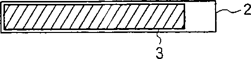
Fig. 3 A is the plane graph of IBR, and Fig. 3 B is the side view of IBR.1BR is made up of the high-insulativity flat-form substrates 31 of 96% aluminium oxide and electrode A, B and the C that forms thereon with ruthenium-oxide family low resistance slurry.By coating ruthenium-oxide family's slurry and curing, in wavy mode between electrode A and the electrode C, form resistor 32 between electrode C and the electrode B.By stacked high pressure resistant, high-insulativity melted glass (being referred to as " outer coating " sometimes) (B
2O
3-SiO
2-PbO family) 33a and 33b come protective resistor 32.In addition, on the surface of the surface opposite that is formed with resistor, form melted glass 33c.By these melted glass are cured covering substrate 31.
Fig. 4 is the enlarged drawing of electrode B near zone.Form thick-layer by silk screen printing coating outer coating 33a, 33b and 33c.These outer coatings work to suppress pin hole PH and bubble BB.When making defective insulation owing to these pin holes and bubble, resistor 32 can be damaged, and therefore in order to guarantee that insulation is enough, forms other two layers of coatings on the resistor 32: the first external application film 33a and the second external application film 33b.Gross thickness is about 0.5mm.With a side opposite surfaces that is formed with resistor 32 on the outer coating 33c that forms be used to prevent form thickness and for example be about 20 μ m from substrate 31 venting.In addition, on electrode A and electrode C distolateral, form outer coating 33d.
The high pressure of about 27kV is added in the electrode A of IBR.This and voltage are that the electrode B of 300~1000V has bigger potential difference.The surface of high-insulativity external application film 33b is recharged, and voltage raises lentamente to electrode B.Finally, with electrode B or with the first grid G of electron gun 20
1, second grid G
2With the 4th grid G
4Discharge, and discharge with resistor 32 again.In conjunction with Figure 14 this discharge condition is described.
Among the IBR, bigger shown in Fig. 5 A at the Bomi degree of electrode B one side resistance device 32.IBR is near electron gun setting shown in Fig. 5 B.Change the Bomi degree of resistor 32, as shown in Figure 6,, shown in (3), and reduce and the 3rd grid G so that reduce electric potential gradient at the resistor at the less position of the wavy density of resistor 32
3The potential difference of (applying anode voltage here).If the use cathode ray tube, the resistor 32 of current direction IBR would be bigger in the heating of high resistance density portion.Therefore, be about 80 ℃, be about 150 ℃ but observe temperature at the high resistance density portion in the heating of low resistance density portion.
Owing to cover the external application film 33a of resistor 32 and the insulating properties height of 33b, so the surface charging of external application film 33b is to high potential.When electron gun was brought into use, as the line (shown in 1) of Fig. 6, to electrode B, current potential was linear the reduction basically from electrode A, but As time goes on, shown in line (2), voltage raises lentamente to electrode B, final and electrode B or with first grid G
1, second grid G
2With the 4th grid G
4Discharge, and discharge with resistor 32 again.When discharge takes place, discharge electric charge, the current potential line of return (1), but along with the time passes once more, electric charge increases once more, in the mode that repeats identical discharge takes place.Since this discharge, external application film 33a and 33b insulation breakdown, resistor 32 is damaged, because the current potential of electrode C changes, so convergence voltage changes, the colour that presents on phosphor screen degenerates.
Insulating properties at this mode IBR is extremely important, therefore in order to guarantee insulation, applies the external application film twice on resistor 32, and the formation integral thickness is 0.4~0.5mm, and finished product IBR is done strict visual examination.So caused lower productivity ratio.
The purpose of this invention is to provide a kind ofly can stably provide dividing potential drop and cheap resistive element that is not recharged and the cathode ray tube with this resistive element.
To achieve these goals, the invention provides a kind of resistive element, it is formed on the substrate by a plurality of resistors, uses its dividing potential drop, and high voltage offered the electron gun of cathode ray tube, wherein part or all of described substrate is by covering as outermost high resistance electric conducting material.
It is better to form the high resistance conductive material layer by the dielectric film of the resistor on the covering substrate.
The high resistance conductive material layer is 10 150 ℃ resistivity
6~10
14Ω m is better.
Form the high resistance conductive material layer so that connection is very good between the electrode of described resistor.
It is very good that substrate is made of the high resistance conductivity ceramics.
And, to achieve these goals, the invention provides a kind of cathode ray tube with resistive element, this resistive element is formed on the substrate by a plurality of resistors, part or all of described substrate is by covering as outermost high resistance electric conducting material, use its dividing potential drop, and high voltage is offered the electron gun of cathode ray tube.
Because resistive element of the present invention has the high resistance conductive material layer that is formed at its outmost surface, thus have only minimum leakage current to flow through this high resistance electric conducting material, thereby current potential is stable, do not charge in the surface.In addition, the current potential of high resistance conductive material layer is proportional to the path of leakage current, is reduced with the potential difference of the resistance current potential that is positioned at the resistor under it.
Owing to there is not any charging, so surface-potential stabilization is reduced with on every side discharge.And, owing to the potential difference with resistor reduces, so be difficult for the discharge of generation and resistor.As a result, external application film and resistor are not had any damage, resistance value is stable for a long time, and it is stable to assemble current potential, thereby does not have any colour shift.
In addition, when covering resistor by dielectric film, be difficult for the discharge to resistor of generation because of existing bubble or pin hole to produce in the dielectric film, so can simplify inspection to the dielectric film outward appearance, perhaps can form dielectric film thinlyyer, sometimes even can omit dielectric film, only cover resistor with a high resistance electric conducting material.Can reduce cost like this.
Below, the accompanying drawings preferred embodiment can more clearly understand above-mentioned and other purposes and feature of the present invention.
Fig. 1 is the configuration schematic diagram of IBR in the cathode ray tube.
Fig. 2 A and 2B are the configuration of IBR and the schematic diagram of electron gun.
Fig. 3 A and 3B are the examples of IBR, and wherein Fig. 3 A is a plane graph, and Fig. 3 B is a side view.
Fig. 4 is near the enlarged drawing at the position of circle of Fig. 3 B.
Fig. 5 A is the plane graph of IBR.
Fig. 5 B is the schematic diagram of electron gun.
Fig. 6 is the potential curve of cathode ray tube in X-direction.
Fig. 7 is the generalized section of resistive element of the present invention.
Fig. 8 A~8C is the pattern that basically forms the high-resistance material layer, and wherein Fig. 8 A is a plane graph, and Fig. 8 B is a side view, and Fig. 8 C is a bottom view.
Fig. 9 A~9C is another pattern that basically forms the high-resistance material layer, and wherein Fig. 9 A is a plane graph, and Fig. 9 B is a side view, and Fig. 9 C is a bottom view.
Figure 10 A~10C is the another pattern that basically forms the high-resistance material layer, and wherein Figure 10 A is a plane graph, and Figure 10 B is a side view, and Figure 10 C is a bottom view.
Figure 11 A~11E is the amplification profile near the zone of electrode B, shows the pattern that is used to basically form the high-resistance material layer.
Figure 12 is the profile of another pattern of resistive element of the present invention.
Figure 13 is a graph of relation between the resistance of institute's making alive and high resistance electric conducting material.
Figure 14 is the temperature characteristics of the resistance of high resistance electric conducting material.
Below preferred embodiments of the present invention will be described, but obviously the present invention is not limited to this.
Fig. 7 is the profile of a kind of pattern of resistive element of the present invention.Notice that the part identical with correlation technique adopts identical reference number.Resistive element 1 for example is made up of the smooth insulating substrate 2 of 96% aluminium oxide and the low resistance electrode A of for example ruthenium-oxide family, B and the C that forms thereon.Between these electrodes, form for example ruthenium-oxide family high resistance resistor 32.Be formed with on the surface of substrate 2 of resistor 32, except electrode, formed high pressure resistant, high-insulativity melted glass (B for example in its whole zone basically
2O
3-SiO
2-PbO family) dielectric film 33, cover resistor 32.In addition, the part of the dielectric film 33 between electrode A and electrode B, high resistance conductive material layer 3 covers dielectric film 33 as outermost layer.Arrange like this, be connected with the electrode B conduction with electrode A.Correlation technique indifference shown in the electrode of resistive element 1 and resistor 32 and Fig. 3 A or the 3B.What therefore, the configuration of resistor, electrode position, electrode configuration were all expected is any.
The high resistance electric conducting material for example is 10 150 ℃ resistivity
6~10
14Ω m.If resistance is higher than this, minimum leakage current is become is difficult to flow, and if resistance less than this, then leakage current becomes excessive, under certain conditions, the power consumption of cathode ray tube becomes excessive.This high resistance electric conducting material for example mainly is made up of lead glass, forms by applying with the glass that contains tin oxide about 10~25% and antimony oxide, then at 500~585 ℃ of sintering.Thickness for example is 0.01~0.05mm, but this is to consider the stability of power loss and surface potential and preferred.It should be noted that and except above-mentioned tin oxide and antimony oxide, iron oxide, manganese oxide etc. can also be arranged as the material of giving conductance.But this is not special restriction.
Shown in Fig. 1 and Fig. 2 A, 2B, this resistive element 1 can be installed near electron gun one side of cathode ray tube, and is used as antianode voltage dividing potential drop and provides deflecting voltage or the IBR of electrode voltage.At this moment, supply with the about 27kV of electrode A, supply with the voltage of electrode B, supply with the voltage of the about 300~1000V of electrode C than these low several kV.Therefore, on high resistance conductive material layer 3, apply high voltage.
Figure 13 is the relation curve that is added between the resistance that the voltage of high resistance electric conducting material and the combined amount by describing to adopt antimony oxide obtain as the measured value of parameter.Line (1) is to have the situation of the lead glass integral body of 15% tin oxide and antimony oxide content at 520 ℃ of sintering; Line (2) is to have the situation of the lead glass integral body of 15% tin oxide and antimony oxide content at 580 ℃ of sintering; Line (3) is to have the situation of the lead glass integral body of 20% tin oxide and antimony oxide content at 580 ℃ of sintering; Line (4) is to have the situation of the lead glass integral body of 25% tin oxide and antimony oxide content at 580 ℃ of sintering.Verified, when tin oxide and antimony oxide content are excessive, the resistance value step-down.Line wherein (2), resistance value was about 10 when anode voltage was 27kV
11Ω is the most desirable.As shown in figure 14, the temperature characterisitic of this high resistance conductivity ceramics, even for example when temperature raises the minor variations along with resistance also be stable.
When 80 ℃ apply 30kV voltage to resistive element shown in Figure 7, measure that (resistivity is 10 at the high resistance conductive material layer
11About Ω cm) in the electric current that flows, find thus, current value no change almost As time goes on, mobile minimum leakage current is stabilized in the scope of 150~200nA.Thus, power consumption is 4.5~6 * 10
-2W, (resistance value is about 10 for this and traditional IBR
9About Ω cm) the power consumption of 1W to compare be extremely low, therefore do not have practical problem.
In this way, owing in outmost surface the high resistance conductive material layer is arranged, and it is minimum to flow through the leakage current of this high resistance conductive material layer, so resistive element of the present invention can not charge in its surface.The electric potential gradient of high resistance conductive material layer becomes the straight line that is proportional to leakage path, shown in (1) among Fig. 6.For example, high resistance conductive material layer 33 is at second grid G
2The current potential of some P on (voltage is about 300V) is stabilized in about 3kV.Among traditional IBR, as shown in Figure 6, because repeatedly charging and discharge, current potential is changed to 3kV from 27kV repeatedly.Because surface-potential stabilization,, be difficult for taking place discharge with electrode B so diminish with the potential difference of electrode B.In addition, since with first grid G
1, second grid G
2With the 4th grid G
4Potential difference also diminishes, and is also difficult to the discharge of these grids.Especially, owing to the potential difference with resistor 32 becomes minimum, so no longer be easy to resistor 32 discharges.And, to the also difficult generation of the discharge of other lead-in wires.
Therefore, dielectric film and resistor are no longer impaired, and it is stable that resistance value keeps for a long time, thereby long-time convergence voltage keeps stable, is difficult for taking place colour cast.
The following manufacturing process of explanation resistive element shown in Figure 7, at first, the low resistance slurry that uses ruthenium-oxide family for example then, adopts the high resistance slurry printed resistor 32 of ruthenium-oxide family at substrate 2 print electrode A, B and C.Then, measured resistance value is finely tuned resistance value to predetermined value.Subsequently, apply for example B by silk screen printing
2O
3-SiO
2-PbO family melted glass forms dielectric film 33, in for example 600 ℃ of roastings.With containing have an appointment 15% the tin oxide and the lead glass slurry coating dielectric film of antimony oxide,, form high resistance conductive material layer 3 by silk screen printing then in for example 580 ℃ of roastings.Make after the resistive element 1, dielectric film 33 is done the visual inspection of bubble or pin hole.In the inspection of dielectric film 33, resistive element 1 of the present invention does not subject to therefore can simplify visual examination, reduce cost because of the discharge to resistor 32 of the bubble of dielectric film 33 or pin hole.
The formation pattern of high resistance ceramic layer is shown in Fig. 8 A~8C to 10A~10C.Fig. 8 A, 9A and 10A are the surface plane figure that is formed with resistor 32 on it, and Fig. 8 B, 9B and 10B are side views, and Fig. 8 C, 9C and 10C are the plane graphs that is formed with surface opposite one side of resistor 32 on it.Fig. 8 A~8C has showed the example that forms high resistance conductive material layer 3 on the surface that only is formed with resistor 32 thereon.Fig. 9 A~9C has showed the example that forms resistive formation on two surfaces, and Figure 10 A~10C has showed the example at two surfaces and side formation resistive formation.Best shown in Figure 10 A~10C in these modes of operation, wherein the whole surface of substrate 2 is capped entirely.Can prevent whole surface charging thus, but be disadvantageous from cost consideration at substrate 22.
The modes of application of high resistance conductive material layer below is described.Figure 11 A~11E is the enlarged drawing near the zone of electrode B.The resistive element 1d of Figure 11 A is traditional two-layer external application film 33a and the example of 33b, stacked high resistance conductive material layer 3 on it.That is electrode A and resistor 32 are formed on the substrate 2, and dielectric film 33d is formed between the end and electrode B of substrate 2.The first dielectric film 33a forms and is formed with thereon on the whole substantially surface of substrate 2 except that electrode of resistor 32.The second dielectric film 33b is stacked on first dielectric film 33.High resistance conductive material layer 3 is arranged on the second dielectric film 33b with the electrode B end with being connected.
The resistive element 1e of Figure 11 B and the configuration of Figure 11 A are basic identical, separate with electrode B but difference is the end of high resistance conductive material layer 3, and electrode B and high resistance conductive material layer 3 are not electrically connected.Even in this way, electrode and high resistance conductive material layer 3 are not electrically connected, and do not have practical problem yet.Usually form high resistance conductive material layer 3 by silk screen printing.In method for printing screen, be difficult to cover downset areas, if thereby adopt this configuration then help making.
The resistive element 1f of Figure 11 C has individual layer dielectric film 33, the stacked high resistance conductive material layer 3 that is electrically connected with electrode B on it.The current potential of the high resistance conductive material layer 3 of close electrode B is stabilized in low level, so the insulation resistance of dielectric film 33 only need be less, need not make dielectric film 33 thicker again.Therefore, shown in Figure 11 C, can be dielectric film 33 from traditional two-layer one deck that is reduced to.At this moment, the thickness of dielectric film 33 can for example be about about 0.2~0.3mm.Even dielectric film 33 is individual layers, shown in Figure 11 D, also can have the high resistance conductive material layer 3 and the electrode B of electric insulation.In addition, when high resistance conductive material layer 3 can not damage or not with resistor 32 reaction, shown in Figure 11 E, then can save dielectric film 33, only cover resistors 32 with high resistance conductive material layer 3, can further reduce cost.As shown in figure 12, can be the substrate 2a that 15% niobium, iron, manganese etc. are made with for example 85% aluminium oxide and all the other, making its resistivity that becomes 150 ℃ is 10
6~10
14The high resistance conductivity ceramics of Ω m.If substrate 2a is made up of this high resistance conductivity ceramics, then minimum at the mobile leakage current of substrate 2a, substrate 2a can not charge, and it is more stable that the current potential of resistive element 1i will become.In addition, can also save with the surface of the surface opposite that is formed with resistor 32 on form high resistance conductivity ceramics film, therefore further reduced cost.
Make after the resistive element, it is assembled into electron gun, this chamber is vacuumized and seals, apply the processing that the voltage that is higher than rated value is called " adjustment " or " arcing ".Variation before and after the resistance value of resistor is managed herein shows that resistor is damaged.
When handling thus when resistive element applies high voltage shown in Fig. 8 A~8C to 10A~10C, the surface that is formed with the high resistance conductive material layer is not luminous, and does not form the surperficial hair powder ruddiness of high resistance conductive material layer.Every kind of situation, the resistance value of resistor is no change almost, and is no problem at all.Therefore, the formation that can confirm the high resistance conductive material layer causes resistive element surface-potential stabilization.
In Fig. 7 and other accompanying drawings, substrate is to show as dull and stereotyped entirely, but also can be cylinder, cylinder or other shapes.Also can make other various improvement that do not depart from the scope of the present invention.
Resistive element of the present invention can the target ray tube the high voltage dividing potential drop, and provide discharge less burning voltage.
In addition, owing to adopt this resistive element to the electron gun dividing potential drop, so cathode ray tube of the present invention can be worked long-term and stably.
Claims (10)
1. resistive element that is used for cathode ray tube comprises:
One substrate;
At least one resistor is configured on the described substrate;
At least one electrode is configured on the described substrate, and links to each other with described at least one resistor; With
One high resistance conductive material layer is configured on described at least one resistor, as the top one deck of described substrate.
2. resistive element according to claim 1 is characterized in that, described high resistance conductive material layer covers on-chip described at least one resistor.
3. resistive element according to claim 1 is characterized in that, the resistivity of material in the time of 150 ℃ that is used for described high resistance conductive material layer is 10
6-10
14Ω m.
4. resistive element according to claim 1 is characterized in that this resistive element has at least two resistors, and described high resistance conductive material layer is connected with the electrode that links to each other with described at least two resistors.
5. resistive element according to claim 1 is characterized in that described substrate is made of the high resistance conductivity ceramics.
6. cathode ray tube comprises:
One electron gun; With
One resistive element is connected with described electron gun, and this resistive element comprises:
One substrate;
A plurality of resistors are configured on the described substrate;
One high resistance conductive material layer is configured on described a plurality of resistor, as
The top one deck of described substrate, wherein said resistive element carries out dividing potential drop to high voltage and it is added on the described electron gun.
7. cathode ray tube according to claim 6 is characterized in that, the high resistance conductive material layer in the described resistive element covers on-chip described a plurality of resistors.
8. cathode ray tube according to claim 6 is characterized in that, the resistivity of material in the time of 150 ℃ that is used for the described high resistance conductive material layer of described resistive element is 10
6-10
14Ω m.
9. cathode ray tube according to claim 6, it is characterized in that, described resistive element has a plurality of electrodes, and these electrodes link to each other with described a plurality of resistors, and in described high resistance conductive material layer and a plurality of electrodes that link to each other with described a plurality of resistors at least two are connected.
10. cathode ray tube according to claim 6 is characterized in that described substrate is made of the high resistance conductivity ceramics.
Applications Claiming Priority (3)
| Application Number | Priority Date | Filing Date | Title |
|---|---|---|---|
| JP135494/96 | 1996-05-29 | ||
| JP8135494A JPH09320482A (en) | 1996-05-29 | 1996-05-29 | Resistor element and cathode-ray tube |
| JP135494/1996 | 1996-05-29 |
Publications (2)
| Publication Number | Publication Date |
|---|---|
| CN1169586A CN1169586A (en) | 1998-01-07 |
| CN1106668C true CN1106668C (en) | 2003-04-23 |
Family
ID=15153058
Family Applications (1)
| Application Number | Title | Priority Date | Filing Date |
|---|---|---|---|
| CN97113254A Expired - Fee Related CN1106668C (en) | 1996-05-29 | 1997-05-29 | resistance element and cathode ray tube |
Country Status (4)
| Country | Link |
|---|---|
| US (1) | US5914559A (en) |
| JP (1) | JPH09320482A (en) |
| CN (1) | CN1106668C (en) |
| SG (1) | SG60036A1 (en) |
Families Citing this family (12)
| Publication number | Priority date | Publication date | Assignee | Title |
|---|---|---|---|---|
| JP3810507B2 (en) * | 1997-03-11 | 2006-08-16 | 松下電器産業株式会社 | Strain sensitive resistor paste |
| DE69938408T2 (en) * | 1998-09-08 | 2009-04-09 | Matsushita Electric Industrial Co., Ltd., Kadoma-shi | Field emission display with oxide resistance |
| JP2000353604A (en) * | 1999-06-10 | 2000-12-19 | Alps Electric Co Ltd | Variable resistor |
| DE60016380T2 (en) * | 1999-10-29 | 2005-10-27 | Koninklijke Philips Electronics N.V. | RESISTANCE ARRANGEMENT AND CATHODE RAY TUBES |
| JP2001202905A (en) * | 2000-01-18 | 2001-07-27 | Hitachi Ltd | Cathode-ray tube |
| JP2001210254A (en) * | 2000-01-28 | 2001-08-03 | Hitachi Ltd | Cathode-ray tube |
| JP2002093344A (en) * | 2000-09-19 | 2002-03-29 | Hitachi Ltd | Color cathode-ray tube |
| US20050049632A1 (en) * | 2002-01-22 | 2005-03-03 | Yukio Inokuti | Ceramic-coated instruments for medical use, ceramic-coated instruments for studying living organisms and process for producing the same |
| CN1292717C (en) * | 2002-01-22 | 2007-01-03 | 杰富意钢铁株式会社 | Ceramic coated medical equipment and biological research equipment and its producing method |
| JP2004121064A (en) * | 2002-10-01 | 2004-04-22 | Jfe Steel Kk | Ceramic-coated needle for controlling gene |
| JP2004200123A (en) * | 2002-12-20 | 2004-07-15 | Toshiba Corp | Resistor for electron gun structure, electron gun structure, and cathode-ray tube |
| WO2004066412A2 (en) * | 2003-01-20 | 2004-08-05 | Lg. Philips Displays | Resistive high-voltage divider, electron gun incorporating a resistive divider and cathode ray tube |
Citations (2)
| Publication number | Priority date | Publication date | Assignee | Title |
|---|---|---|---|---|
| US4349767A (en) * | 1977-01-17 | 1982-09-14 | Sony Corporation | Cathode ray tube resistance of ruthenium oxide and glass containing alumina powder |
| JPH0911246A (en) * | 1995-07-03 | 1997-01-14 | Kanto Auto Works Ltd | Production of interior material |
Family Cites Families (2)
| Publication number | Priority date | Publication date | Assignee | Title |
|---|---|---|---|---|
| JP3576217B2 (en) * | 1993-09-30 | 2004-10-13 | 株式会社東芝 | Picture tube device |
| JP3586286B2 (en) * | 1993-12-14 | 2004-11-10 | 株式会社東芝 | Color picture tube |
-
1996
- 1996-05-29 JP JP8135494A patent/JPH09320482A/en active Pending
-
1997
- 1997-01-23 SG SG1997000155A patent/SG60036A1/en unknown
- 1997-05-16 US US08/857,835 patent/US5914559A/en not_active Expired - Fee Related
- 1997-05-29 CN CN97113254A patent/CN1106668C/en not_active Expired - Fee Related
Patent Citations (2)
| Publication number | Priority date | Publication date | Assignee | Title |
|---|---|---|---|---|
| US4349767A (en) * | 1977-01-17 | 1982-09-14 | Sony Corporation | Cathode ray tube resistance of ruthenium oxide and glass containing alumina powder |
| JPH0911246A (en) * | 1995-07-03 | 1997-01-14 | Kanto Auto Works Ltd | Production of interior material |
Also Published As
| Publication number | Publication date |
|---|---|
| CN1169586A (en) | 1998-01-07 |
| JPH09320482A (en) | 1997-12-12 |
| SG60036A1 (en) | 1999-02-22 |
| US5914559A (en) | 1999-06-22 |
Similar Documents
| Publication | Publication Date | Title |
|---|---|---|
| CN1106668C (en) | resistance element and cathode ray tube | |
| US4786842A (en) | Resistor assembly | |
| KR910009245B1 (en) | Resistors for cathode ray tube | |
| US4647815A (en) | Resistors for use in cathode ray tubes | |
| US7385345B2 (en) | Electron emission device | |
| CN1104018C (en) | Cathod ray tube comprisijg a heating element | |
| KR100253067B1 (en) | Color cathode ray tube | |
| US6005472A (en) | Inner resistor for cathode-ray tube | |
| KR100659050B1 (en) | Electron gun with resistor and capacitor | |
| US7764011B2 (en) | Electron emission display device | |
| CN1344007A (en) | CRT having internal bleeder resistor | |
| US6917151B2 (en) | Resistor for electron gun assembly, electron gun assembly, and cathode-ray tube | |
| JPS60124340A (en) | Resistor built in cathode ray tube | |
| US20020074949A1 (en) | Method for producing a resistor | |
| US6495966B2 (en) | Field emission display including a resistor | |
| JPS6313242A (en) | Resistor incorporated in cathode-ray tube | |
| JPS62207742A (en) | Glass paste for built-in resistor in cathode ray tube | |
| CN1572010A (en) | Election gun assembly resistor and cathode ray tube | |
| JPS61116735A (en) | Built-in resistor of cathode ray tube | |
| US20080211382A1 (en) | Image display device | |
| JPH0785403B2 (en) | Built-in resistor of cathode ray tube | |
| JPS61250935A (en) | Inner resistor of cathode-ray tube | |
| JPS63184231A (en) | Knocking process for cathode-ray tube | |
| JPH06168668A (en) | Cathode structure for dc type discharge display tube | |
| JPS60227342A (en) | Cathode-ray tube device |
Legal Events
| Date | Code | Title | Description |
|---|---|---|---|
| C06 | Publication | ||
| PB01 | Publication | ||
| C10 | Entry into substantive examination | ||
| SE01 | Entry into force of request for substantive examination | ||
| C14 | Grant of patent or utility model | ||
| GR01 | Patent grant | ||
| C19 | Lapse of patent right due to non-payment of the annual fee | ||
| CF01 | Termination of patent right due to non-payment of annual fee |