CN100374283C - Microfluidic articles and method of manufacturing same - Google Patents
Microfluidic articles and method of manufacturing same Download PDFInfo
- Publication number
- CN100374283C CN100374283C CNB998073776A CN99807377A CN100374283C CN 100374283 C CN100374283 C CN 100374283C CN B998073776 A CNB998073776 A CN B998073776A CN 99807377 A CN99807377 A CN 99807377A CN 100374283 C CN100374283 C CN 100374283C
- Authority
- CN
- China
- Prior art keywords
- substrate
- polymer matrix
- matrix film
- microfluidic process
- microfluidic
- Prior art date
- Legal status (The legal status is an assumption and is not a legal conclusion. Google has not performed a legal analysis and makes no representation as to the accuracy of the status listed.)
- Expired - Lifetime
Links
Images


Classifications
-
- B—PERFORMING OPERATIONS; TRANSPORTING
- B01—PHYSICAL OR CHEMICAL PROCESSES OR APPARATUS IN GENERAL
- B01L—CHEMICAL OR PHYSICAL LABORATORY APPARATUS FOR GENERAL USE
- B01L3/00—Containers or dishes for laboratory use, e.g. laboratory glassware; Droppers
- B01L3/50—Containers for the purpose of retaining a material to be analysed, e.g. test tubes
- B01L3/502—Containers for the purpose of retaining a material to be analysed, e.g. test tubes with fluid transport, e.g. in multi-compartment structures
- B01L3/5027—Containers for the purpose of retaining a material to be analysed, e.g. test tubes with fluid transport, e.g. in multi-compartment structures by integrated microfluidic structures, i.e. dimensions of channels and chambers are such that surface tension forces are important, e.g. lab-on-a-chip
- B01L3/502707—Containers for the purpose of retaining a material to be analysed, e.g. test tubes with fluid transport, e.g. in multi-compartment structures by integrated microfluidic structures, i.e. dimensions of channels and chambers are such that surface tension forces are important, e.g. lab-on-a-chip characterised by the manufacture of the container or its components
-
- B—PERFORMING OPERATIONS; TRANSPORTING
- B29—WORKING OF PLASTICS; WORKING OF SUBSTANCES IN A PLASTIC STATE IN GENERAL
- B29C—SHAPING OR JOINING OF PLASTICS; SHAPING OF MATERIAL IN A PLASTIC STATE, NOT OTHERWISE PROVIDED FOR; AFTER-TREATMENT OF THE SHAPED PRODUCTS, e.g. REPAIRING
- B29C59/00—Surface shaping of articles, e.g. embossing; Apparatus therefor
- B29C59/02—Surface shaping of articles, e.g. embossing; Apparatus therefor by mechanical means, e.g. pressing
- B29C59/04—Surface shaping of articles, e.g. embossing; Apparatus therefor by mechanical means, e.g. pressing using rollers or endless belts
-
- B—PERFORMING OPERATIONS; TRANSPORTING
- B01—PHYSICAL OR CHEMICAL PROCESSES OR APPARATUS IN GENERAL
- B01L—CHEMICAL OR PHYSICAL LABORATORY APPARATUS FOR GENERAL USE
- B01L3/00—Containers or dishes for laboratory use, e.g. laboratory glassware; Droppers
- B01L3/50—Containers for the purpose of retaining a material to be analysed, e.g. test tubes
- B01L3/505—Containers for the purpose of retaining a material to be analysed, e.g. test tubes flexible containers not provided for above
-
- B—PERFORMING OPERATIONS; TRANSPORTING
- B29—WORKING OF PLASTICS; WORKING OF SUBSTANCES IN A PLASTIC STATE IN GENERAL
- B29C—SHAPING OR JOINING OF PLASTICS; SHAPING OF MATERIAL IN A PLASTIC STATE, NOT OTHERWISE PROVIDED FOR; AFTER-TREATMENT OF THE SHAPED PRODUCTS, e.g. REPAIRING
- B29C39/00—Shaping by casting, i.e. introducing the moulding material into a mould or between confining surfaces without significant moulding pressure; Apparatus therefor
- B29C39/14—Shaping by casting, i.e. introducing the moulding material into a mould or between confining surfaces without significant moulding pressure; Apparatus therefor for making articles of indefinite length
- B29C39/148—Shaping by casting, i.e. introducing the moulding material into a mould or between confining surfaces without significant moulding pressure; Apparatus therefor for making articles of indefinite length characterised by the shape of the surface
-
- B—PERFORMING OPERATIONS; TRANSPORTING
- B29—WORKING OF PLASTICS; WORKING OF SUBSTANCES IN A PLASTIC STATE IN GENERAL
- B29C—SHAPING OR JOINING OF PLASTICS; SHAPING OF MATERIAL IN A PLASTIC STATE, NOT OTHERWISE PROVIDED FOR; AFTER-TREATMENT OF THE SHAPED PRODUCTS, e.g. REPAIRING
- B29C43/00—Compression moulding, i.e. applying external pressure to flow the moulding material; Apparatus therefor
- B29C43/22—Compression moulding, i.e. applying external pressure to flow the moulding material; Apparatus therefor of articles of indefinite length
- B29C43/222—Compression moulding, i.e. applying external pressure to flow the moulding material; Apparatus therefor of articles of indefinite length characterised by the shape of the surface
-
- B—PERFORMING OPERATIONS; TRANSPORTING
- B29—WORKING OF PLASTICS; WORKING OF SUBSTANCES IN A PLASTIC STATE IN GENERAL
- B29C—SHAPING OR JOINING OF PLASTICS; SHAPING OF MATERIAL IN A PLASTIC STATE, NOT OTHERWISE PROVIDED FOR; AFTER-TREATMENT OF THE SHAPED PRODUCTS, e.g. REPAIRING
- B29C59/00—Surface shaping of articles, e.g. embossing; Apparatus therefor
- B29C59/02—Surface shaping of articles, e.g. embossing; Apparatus therefor by mechanical means, e.g. pressing
- B29C59/022—Surface shaping of articles, e.g. embossing; Apparatus therefor by mechanical means, e.g. pressing characterised by the disposition or the configuration, e.g. dimensions, of the embossments or the shaping tools therefor
-
- B—PERFORMING OPERATIONS; TRANSPORTING
- B01—PHYSICAL OR CHEMICAL PROCESSES OR APPARATUS IN GENERAL
- B01L—CHEMICAL OR PHYSICAL LABORATORY APPARATUS FOR GENERAL USE
- B01L2200/00—Solutions for specific problems relating to chemical or physical laboratory apparatus
- B01L2200/12—Specific details about manufacturing devices
-
- B—PERFORMING OPERATIONS; TRANSPORTING
- B01—PHYSICAL OR CHEMICAL PROCESSES OR APPARATUS IN GENERAL
- B01L—CHEMICAL OR PHYSICAL LABORATORY APPARATUS FOR GENERAL USE
- B01L2300/00—Additional constructional details
- B01L2300/08—Geometry, shape and general structure
- B01L2300/0809—Geometry, shape and general structure rectangular shaped
- B01L2300/0816—Cards, e.g. flat sample carriers usually with flow in two horizontal directions
-
- B—PERFORMING OPERATIONS; TRANSPORTING
- B01—PHYSICAL OR CHEMICAL PROCESSES OR APPARATUS IN GENERAL
- B01L—CHEMICAL OR PHYSICAL LABORATORY APPARATUS FOR GENERAL USE
- B01L2300/00—Additional constructional details
- B01L2300/08—Geometry, shape and general structure
- B01L2300/0887—Laminated structure
-
- B—PERFORMING OPERATIONS; TRANSPORTING
- B01—PHYSICAL OR CHEMICAL PROCESSES OR APPARATUS IN GENERAL
- B01L—CHEMICAL OR PHYSICAL LABORATORY APPARATUS FOR GENERAL USE
- B01L2400/00—Moving or stopping fluids
- B01L2400/04—Moving fluids with specific forces or mechanical means
- B01L2400/0403—Moving fluids with specific forces or mechanical means specific forces
- B01L2400/0415—Moving fluids with specific forces or mechanical means specific forces electrical forces, e.g. electrokinetic
-
- G—PHYSICS
- G01—MEASURING; TESTING
- G01N—INVESTIGATING OR ANALYSING MATERIALS BY DETERMINING THEIR CHEMICAL OR PHYSICAL PROPERTIES
- G01N35/00—Automatic analysis not limited to methods or materials provided for in any single one of groups G01N1/00 - G01N33/00; Handling materials therefor
- G01N35/00009—Automatic analysis not limited to methods or materials provided for in any single one of groups G01N1/00 - G01N33/00; Handling materials therefor provided with a sample supporting tape, e.g. with absorbent zones
-
- Y—GENERAL TAGGING OF NEW TECHNOLOGICAL DEVELOPMENTS; GENERAL TAGGING OF CROSS-SECTIONAL TECHNOLOGIES SPANNING OVER SEVERAL SECTIONS OF THE IPC; TECHNICAL SUBJECTS COVERED BY FORMER USPC CROSS-REFERENCE ART COLLECTIONS [XRACs] AND DIGESTS
- Y10—TECHNICAL SUBJECTS COVERED BY FORMER USPC
- Y10S—TECHNICAL SUBJECTS COVERED BY FORMER USPC CROSS-REFERENCE ART COLLECTIONS [XRACs] AND DIGESTS
- Y10S428/00—Stock material or miscellaneous articles
- Y10S428/906—Roll or coil
-
- Y—GENERAL TAGGING OF NEW TECHNOLOGICAL DEVELOPMENTS; GENERAL TAGGING OF CROSS-SECTIONAL TECHNOLOGIES SPANNING OVER SEVERAL SECTIONS OF THE IPC; TECHNICAL SUBJECTS COVERED BY FORMER USPC CROSS-REFERENCE ART COLLECTIONS [XRACs] AND DIGESTS
- Y10—TECHNICAL SUBJECTS COVERED BY FORMER USPC
- Y10T—TECHNICAL SUBJECTS COVERED BY FORMER US CLASSIFICATION
- Y10T428/00—Stock material or miscellaneous articles
- Y10T428/24—Structurally defined web or sheet [e.g., overall dimension, etc.]
- Y10T428/24479—Structurally defined web or sheet [e.g., overall dimension, etc.] including variation in thickness
- Y10T428/24562—Interlaminar spaces
-
- Y—GENERAL TAGGING OF NEW TECHNOLOGICAL DEVELOPMENTS; GENERAL TAGGING OF CROSS-SECTIONAL TECHNOLOGIES SPANNING OVER SEVERAL SECTIONS OF THE IPC; TECHNICAL SUBJECTS COVERED BY FORMER USPC CROSS-REFERENCE ART COLLECTIONS [XRACs] AND DIGESTS
- Y10—TECHNICAL SUBJECTS COVERED BY FORMER USPC
- Y10T—TECHNICAL SUBJECTS COVERED BY FORMER US CLASSIFICATION
- Y10T428/00—Stock material or miscellaneous articles
- Y10T428/24—Structurally defined web or sheet [e.g., overall dimension, etc.]
- Y10T428/24479—Structurally defined web or sheet [e.g., overall dimension, etc.] including variation in thickness
- Y10T428/2457—Parallel ribs and/or grooves
-
- Y—GENERAL TAGGING OF NEW TECHNOLOGICAL DEVELOPMENTS; GENERAL TAGGING OF CROSS-SECTIONAL TECHNOLOGIES SPANNING OVER SEVERAL SECTIONS OF THE IPC; TECHNICAL SUBJECTS COVERED BY FORMER USPC CROSS-REFERENCE ART COLLECTIONS [XRACs] AND DIGESTS
- Y10—TECHNICAL SUBJECTS COVERED BY FORMER USPC
- Y10T—TECHNICAL SUBJECTS COVERED BY FORMER US CLASSIFICATION
- Y10T428/00—Stock material or miscellaneous articles
- Y10T428/24—Structurally defined web or sheet [e.g., overall dimension, etc.]
- Y10T428/24479—Structurally defined web or sheet [e.g., overall dimension, etc.] including variation in thickness
- Y10T428/24612—Composite web or sheet
-
- Y—GENERAL TAGGING OF NEW TECHNOLOGICAL DEVELOPMENTS; GENERAL TAGGING OF CROSS-SECTIONAL TECHNOLOGIES SPANNING OVER SEVERAL SECTIONS OF THE IPC; TECHNICAL SUBJECTS COVERED BY FORMER USPC CROSS-REFERENCE ART COLLECTIONS [XRACs] AND DIGESTS
- Y10—TECHNICAL SUBJECTS COVERED BY FORMER USPC
- Y10T—TECHNICAL SUBJECTS COVERED BY FORMER US CLASSIFICATION
- Y10T428/00—Stock material or miscellaneous articles
- Y10T428/24—Structurally defined web or sheet [e.g., overall dimension, etc.]
- Y10T428/24744—Longitudinal or transverse tubular cavity or cell
-
- Y—GENERAL TAGGING OF NEW TECHNOLOGICAL DEVELOPMENTS; GENERAL TAGGING OF CROSS-SECTIONAL TECHNOLOGIES SPANNING OVER SEVERAL SECTIONS OF THE IPC; TECHNICAL SUBJECTS COVERED BY FORMER USPC CROSS-REFERENCE ART COLLECTIONS [XRACs] AND DIGESTS
- Y10—TECHNICAL SUBJECTS COVERED BY FORMER USPC
- Y10T—TECHNICAL SUBJECTS COVERED BY FORMER US CLASSIFICATION
- Y10T428/00—Stock material or miscellaneous articles
- Y10T428/31504—Composite [nonstructural laminate]
- Y10T428/31678—Of metal
Landscapes
- Chemical & Material Sciences (AREA)
- Health & Medical Sciences (AREA)
- Mechanical Engineering (AREA)
- Engineering & Computer Science (AREA)
- Chemical Kinetics & Catalysis (AREA)
- Clinical Laboratory Science (AREA)
- Hematology (AREA)
- General Health & Medical Sciences (AREA)
- Analytical Chemistry (AREA)
- Dispersion Chemistry (AREA)
- Micromachines (AREA)
- Physical Or Chemical Processes And Apparatus (AREA)
- Shaping Of Tube Ends By Bending Or Straightening (AREA)
- Exposure Of Semiconductors, Excluding Electron Or Ion Beam Exposure (AREA)
- Casting Or Compression Moulding Of Plastics Or The Like (AREA)
Abstract
A process for preparing a molded article that includes: (a) bringing a moldable material (10) and an open molding tool (16) comprising a molding surface into line contact with each other to imprint a microfluid processing architecture pattern onto the moldable material (10) and thereby form a molded article; and (b) separating the molded article from said molding surface. The invention also features various microfluid processing architecture-bearing, polymeric articles.
Description
Technical field
The present invention relates to microfluidic articles and manufacture method thereof.
Background technology
Tried hard to reduce to analyze size with the parts of other method operation liquid sample such as biological liquid sample.Reduce size and can bring many advantages, comprise the speed that to analyze very little sample, increase analysis, the reagent that can use reduction and minimizing totle drilling cost.
The various parts that are used for the microfluid utilization have been proposed.These parts typically comprise glass or the silicon chip that has the lithographic printing pattern, and etched surface has the structure of one or more formation microfluidic process.Plastic substrate such as polyimides, polyester and Merlon have also been proposed.
The microfluidic articles that needs a kind of condensate base, it can commercial scale amount High-efficient Production, as the form with scroll, and optionally manufactures and has various difference in functionalitys, comprises analytic function.Therefore, first aspect of the present invention is the method for preparing moulding article, comprises making a kind of moldable material, contacts each other in line with the surface of spacious film molding mold, thereby the microfluidic process structure is stamped on the mouldable material.Isolate the moulding article that obtains from the molded surface of mould then.
Summary of the invention
" microfluidic process structure " is meant one or more fluid handling structures of arranging in predetermined self-contained (self-contained) pattern mode.Preferably, this structure comprises that at least a size is not more than the structure of 1000 μ m.In addition, liquid should enter and leave this structure with Z-direction (promptly being into vertical direction with the plane of structure).For the present invention, suitable microfluidic process configuration example comprises the structure that is selected from microchannel, liquid reservoir, sample treatment zone and their combination.
" open mould " is the mould of the annular seal space that exists in the hypodactylia mold closing, as is used for the mould of the type of injection moulding.
" line contact " is meant mould and the moldable material state of contact of being determined by the line that is moved into respect to mould and moldable material.
In one embodiment, moldable material is printable polymerization substrate.The surface that the microfluidic process structure plan is stamped in the polymerization substrate produces molded products.
In another embodiment, but moldable material is the stir-in resin composition.A kind of example of this composition is curable resin combination, and in the case, this method is included in before the goods of molded surface separation molding composition is exposed under heat radiation or the actinic radiation with hardening composition." curing " used herein and " curable resin composition " comprise the resin of crosslinked polymerization, and polymerization single polymerization monomer or oligomer composition, and its product is not must be crosslinked thermosetting resin.The example of preferred curable resin composition is photopolymerizable composition, when contacting with molded surface, solidifies by composition is exposed to actinic radiation.
But another example of stir-in resin composition is the thermoplastic compounds of fusion, the curing thereby it is cooled when the contact molded surface.
When but moldable material is the stir-in resin composition, two preferred molding methods are arranged.In a method for optimizing, but the stir-in resin composition be introduced on the first type surface of polymerization substrate, substrate and swager are respect to one another to be moved, line contacts but make swager and stir-in resin composition become each other.This net result is a double-layer structure, and the layer that wherein has the microfluidic process structure integrally is incorporated into the polymerization substrate.
When but but die material is the stir-in resin composition, another preferred molding methods, but comprise the stir-in resin composition is guided on the stamper surface of swager.But the polymerization substrate and stir-in resin combination of compositions that separates can be produced double-layer structure, the substrate that wherein has the microfluidic process structure integrally is incorporated into the polymerization substrate.
Substrate can combine with the goods of pressing mold, forms to cover the structural cover layer of microfluidic process.Preferably, this substrate is the polymerization substrate.The goods of pressing mold also can be equipped with one or more microelectronic elements, micro optical element and/or slight type mechanical organ.Can various distinct methods in conjunction with these micro elements, show the flexibility of total method.For example, but when die material was printable polymerization substrate, this substrate can comprise micro element.But but when die material be stir-in resin composition and this method when being included in molding with resin combination and polymerization substrate in conjunction with the time, this polymer matrix film can comprise micro element.Also may be in cover layer, to comprise micro element.The form of separating substrate (preferably being a polymerization substrate) that these micro elements also can combine with moulding article provides.
Preferably, this method is designed to a continued operation method.Therefore, but die material is introduced the pressing mold zone of being determined by swager continuously, but and swager continuously contact the structure of a plurality of microfluidic process of generation with the die material line.Preferably, this continuation method obtains the goods of roll form, and it comprises the structure of many microfluidic process.This scroll can directly use or be divided into subsequently multiple independently parts.Additional polymer matrix film can combine with goods continuously.Example comprises cover layer and has the layer of microelectronics, micro-optics and/or micromechanical component.
Another aspect of the present invention, goods comprise (A) stiff first polymerization substrate, and this first polymer matrix film has first first type surface, and this first first type surface comprises the microfluidic process structure (as mentioned above) and second first type surface; (B) the second polymerization substrate, it integrally is incorporated into second first type surface of first substrate.When not having first substrate, this second substrate can form independently substrate.It provides mechanical support for first substrate and provides other element (as microelectronics, micro-optics and/or micromechanical component) is joined the means in the goods, thereby the flexibility of design is provided.
" non-resilient " material is meant in Z direction (promptly the plane to substrate is vertical direction) goes up the not enough material of elasticity, and when to Z direction circulation change power, it can be used as pump or valve.
" combination integrally " is meant that two substrates directly interosculate, rather than by intermediate materials (as adhesive) combination.
Goods preferably comprise and cover the structural cover layer of microfluidic process.This cover layer can be incorporated into the first surface of first substrate, preferably polymeric layer.
Goods preferably comprise one or more microelectronics, micro-optics and/or micromechanical component.These micro elements can be included in first substrate, second substrate, polymer covering or their combination.
The third aspect, goods of the present invention are scroll, and it comprises first polymer matrix film that has first first type surface (comprising a plurality of discontinuous microfluidic process structures (as mentioned above)) and second first type surface.These goods preferably comprise second polymer matrix film, and it integrally is incorporated into second first type surface of (as mentioned above) first substrate.When first substrate did not exist, this second substrate can form independently substrate.
Goods preferably comprise the polymer covering of first first type surface that is incorporated into first substrate.
Goods preferably comprise one or more microelectronics, micro-optics and/or micromechanical component.These micro elements can be included in first substrate, second substrate, polymer covering or their combination.
A fourth aspect of the present invention, goods comprise (A) first polymer matrix film, and this first polymer matrix film has first first type surface, and this first first type surface comprises the microfluidic process structure (as mentioned above) and second first type surface; (B) second polymer matrix film.First first type surface of this second substrate integrally is incorporated into second first type surface of (as mentioned above) first substrate, and second first type surface comprises one or more microelectronic elements and the passage that extends between first and second first type surfaces of second substrate.This second substrate can form independently substrate when not having first substrate.
A fifth aspect of the present invention, goods comprise first polymer matrix film, this first polymer matrix film has first first type surface, this first first type surface comprises the microfluidic process structure (as mentioned above) and second first type surface, and this second surface comprises one or more microelectronic elements and the passage that extends between first and second first type surfaces of this substrate.
A sixth aspect of the present invention, goods comprise (A) first polymer matrix film, and this first polymer matrix film has first first type surface, and this first first type surface comprises the microfluidic process structure (as mentioned above) and second first type surface; (B) polymer covering.This cover layer comprises first first type surface and second first type surface of covering substrate first first type surface, and this second first type surface comprises one or more microelectronic elements and the passage that extends between these tectal first and second first type surfaces.
A seventh aspect of the present invention, a kind of method of handling microfluid sample comprises that (a) provides the goods of roll form, these goods comprise the polymer matrix film that has first first type surface (comprising a plurality of discontinuous microfluidic process structures) and second first type surface; (b) microfluid sample is added one of them microfluidic process structure; (c) handle sample (as passing through analytic sample).
The invention provides the polymer product that is used for handling (as analyzing) microfluid sample, it can commercial scale continuous production, and the form of goods is scroll easily, is easy to storage and carries.This scroll product can be directly used in the processing fluid sample, as uses the reel-to-reel continuation method, comprises that different liquid is injected each microfluidic process structure carries out multiple operation then.In addition, after manufacturing, this scroll product can be divided into a plurality of discontinuous parts.
The method of this manufacturing provides significant design flexibility, and a large amount of procedure of processings can onlinely be carried out.For example, in manufacture process, be easy to by various method, this element is as the part that comprises the substrate that has the microfluidic process structure, as tectal a part or whole part be incorporated into the part of second polymer matrix film of substrate, microelectronics, micro-optics and/or micromechanical component are incorporated into goods.Various designs in conjunction with these micro elements also can be arranged.Also can prepare multi-layer product.
This molding methods is fully general to forming various microfluidic process structural design.Therefore, goods can manufacture has various functions, comprises that for example electrophoresis, the dynamics of capillary tubing suppress to measure, competition immunoassays, enzymatic determination, nucleic acid hybridization mensuration, cell classification, combinatorial chemistry and electrochromatography.
This molding methods can prepare the microfluidic process structure with height aspect ratio and thin portions of various different aspect ratios (feature).This provides the structure that shows improved speed and resolution ratio again.For example, when keeping constant microchannel width, the variable depthization of microchannel.Such microchannel can be used to make up the diffuser of the vertical taper entrance and exit of the micropump be used for piezoelectricity valve one less diffuser (diffuser), or is used to provide electric zone control or Power focus.Similarly, can progressively reduce the width of high aspect ratio microchannel in the constant degree of depth.The structure that the result obtains also can be used for providing electric zone control.
Also can progressively reduce the degree of depth and the width of microchannel, obtain constant cross-sectional area or constant section girth.The result of constant cross-sectional area or girth, the structure that obtains can be embodied as main electrophoresis stream or EOF in the length of whole passage provides constant voltage gradient, thereby seals (not losing resolution capability) for unimolecule mensuration provides light.This structure also can be used for providing the transformation between high and the low aspect-ratio structure (as probe capture region, little well reactor or the piezoelectric driver element of high aspect ratio injection threeway, low aspect ratio), and does not lose the electrokinetics resolving power.
Also can prepare two crossing microchannels that different depth is arranged.Therefore, can utilize this feature to make the microfluid switch again at hydrophobic substrate.Because the difference of the degree of depth, the liquid that can not in the arm of more shallow microchannel is crossed the intersection, unless buffer solution is introduced darker bridge joint intersection, microchannel.The feature of this different depth also can be used for preparing binding post array (post array), is used for immunoassays or nucleic acid determination and probe is captured globule flocks together, and allow indicator and fluid sample freely to flow through simultaneously.
Other features and advantages of the present invention can clearly from the description of following preferred embodiment and claim be found out.
Description of drawings
Fig. 1 is the schematic diagram of " curtain coating (cast) and curing " continuously method of preparation microfluidic articles.
Fig. 1 (a) is the perspective view by the microfluidic articles of method preparation shown in Figure 1.
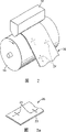
Fig. 2 is the perspective view of " extruding impression " continuously method of preparation microfluidic articles.
Fig. 2 (a) is the perspective view by the microfluidic articles of method preparation shown in Figure 2.
Fig. 3 is the perspective view that " pushes and impress " second example of method continuously of preparation microfluidic articles.
Fig. 3 (a) is the perspective view by the microfluidic articles of method preparation shown in Figure 3.
Fig. 4 is the perspective view that " pushes and impress " the 3rd example of method continuously of preparation microfluidic articles.
Fig. 4 (a) is the perspective view by the microfluidic articles of method preparation shown in Figure 4.
Fig. 5 is the schematic diagram that " pushes and impress " the 4th example of method continuously of preparation microfluidic articles.
Fig. 5 (a) is the perspective view by the microfluidic articles of method preparation shown in Figure 5.
Fig. 6 is the perspective view of continuous " substrate impression " method of preparation microfluidic articles.
Fig. 6 (a) is the perspective view by the microfluidic articles of method preparation shown in Figure 6.
Fig. 7 is the perspective view of second example of continuous " substrate impression " method of preparation microfluidic articles.
Fig. 7 (a) is the perspective view by the microfluidic articles of method preparation shown in Figure 7.
Fig. 8 is the schematic diagram of preparation microfluidic articles continuation method, and wherein cover layer is to be laminated to have the on-chip of microfluidic structures behind molding.
Fig. 9 (a) and 9 (b) are the profiles that has the substrate of microfluidic process structure and the cover layer combination of microelectronic element is housed.
Figure 10 (a) and 10 (b) are the schematic diagrames that shows typical microfluidic process structural design.
Figure 11 (a) has the top view of the flexible polymer substrate of many conducting wires and contact pins.
Figure 11 (b) has the top view of the flexible polymer substrate of a plurality of microfluidic process architectural features on the substrate first type surface.
Figure 12 aims at the substrate shown in Figure 11 (a) to be laminated to the on-chip top view shown in Figure 11 (b).
The specific embodiment
Feature of the present invention is a kind of goods that have the microfluidic process structure of polymer base, the continuous reel-to-reel method that is used for handling (as analyzing) microfluid sample and makes this goods.Fig. 1 has shown an example (being called " curtain coating and curing continuously " method) of this method.Referring to Fig. 1, one is flowable, preferably solvent-free basically, and photocurable resin combination 10 is expressed on the surface of the optically transparent substrate 14 of continuous flexible from die head 12.
The suitable examples of material that is used for substrate 14 comprises poly-(methyl methacrylate) Merlon, polyester and polyimides.The example of the photocurable resin combination that is fit to comprises alkyl acrylate and alkyl methacrylate (as polymethyl methacrylate).This composition also comprises light trigger.The example of the light trigger that is fit to comprises benzoin ether such as benzoin methylether and benzoin iso-propylether; The acetophenone that replaces is as 2,2-diethoxy acetophenone, 2,2-dimethoxy-2-phenyl-1-phenyl acetophenone and dimethoxy hydroxyl acetophenone; α-the keto-alcohol that replaces is as 2-methyl-2-hydroxypropiophenone; The aromatics sulfonic acid chloride is as the 2-naphthalene sulfonyl chloride; With the photonasty oxime, as 1-phenyl-1,2-propanedione-2-(O-ethoxy carbonyl) oxime.Other component that can join in the composition comprises monohydroxy and polyol, the woven webs and the nonwoven web of thixotropic agent, plasticizer, flexibilizer, pigment, filler, abrasive particle, stabilizing agent, light stabilizer, antioxidant, flowable, thickener, delustering agent, colouring agent, adhesive, blowing agent, fungicide, bactericide, surfactant, glass and ceramic bead and reinforcing material such as organic or inorfil.
Resin 10 is contacted with the stamper surface of substrate 14 with swager 16, required microfluidic process structure plan is impressed into the surface of resin bed 10.As shown in Figure 1, swager 16 is with the form of scroll or the form of the endless belt that rotates in the direction of the clock.Yet it also can be the form of cylindrical sleeves.Available various control technology prepares swager, comprises laser ablation control, el, photoetching, X-X-ray lithography X, mechanical annular knurl and line.It has required microfluidic process structure plan.
The operation of carrying out with goods is depended in the design of ad hoc structure.Figure 10 (a), 10 (b) and 11 (b) have shown typical design.These designs comprise competition assay chip (Figure 10 (a)) and ladder type chip (Figure 10 (b)) and electrophoresis chip (Figure 11 (b)).The characteristics of this structure are the various combinations that microchannel, fluid reservoir and sample treatment zone are arranged.Figure 10 (a) and (b) in the single microarchitecture that shows be of a size of the representational typical sizes that is used for these chips.The specific dimensions of any chip is variable.
Make resin bed 10 become line to contact with the surface of revolution of swager 16.Line 11 is to be determined by the upstream edge of resin bed 10, and when swager 16 rotations, moves with respect to swager 16 and resin bed 10.Substrate 14 keeps contacting with resin bed 10, and resin bed also contacts with the surface of swager 16.Any unnecessary resin is reduced to after the minimum, swager 16, substrate 14 and resin bed 10 are exposed under the actinic radiation that is sent by radiation source 18, and (preferably being the form of ultra-violet radiation) solidifies the resin combination that still contacts with the stamper surface of swager 16.The characteristic of every kind of resin combination is depended in the selection of radiated time, dosage height, comprises the thickness of resin bed 10.
Shown in Fig. 1 (a), the product 20 that obtains is two-layer sheets, and polymer matrix film 22 has a plurality of microfluidic process structures 24, and integrally is incorporated into substrate 14.Behind the pressing mold, this sheet can be wound on (not demonstration on the figure) on the roller, obtain the product of roll form.
Also but the available heat curable resin composition is implemented curtain coating and curing as the stir-in resin composition, in the case, then uses infrared source (as heating lamp) to substitute actinic radiation.
In a kind of variation pattern of this method, but the thermoplastic resin of available fusion is as the stir-in resin composition.The assembly of contact back cooling swager and resin makes hardening of resin (rather than curing).
Also can prepare microfluidic articles by the extruding method for stamping.Fig. 2-5 has shown the various example of this method.Referring to as Fig. 2, but directly push the stir-in resin composition to the surface of revolution of swager 16 from die head 12, resin becomes line to contact with the surface of revolution of swager 16 like this; The example of the resin combination that is fit to comprises above-mentioned photocurable, heat cure and thermoplastic resin composition.Line is determined by the upstream edge of resin, and when swager 16 rotations, it moves with respect to swager 16 and resin.Shown in Fig. 2 (a), the product that the result obtains is the single layer articles 26 of sheet form, and its polymer matrix film 23 is to have a plurality of microfluidic process structures 24.This sheet can be wound on (not demonstration on the figure) on the roller, obtain the goods of scroll thing form.
Fig. 3 has shown another variation of extruding method for stamping shown in Figure 2.As shown in Figure 3, polymer matrix film 28 is introduced pressing mold zone (being determined by swager 16), and become line to contact with the rotation stamper surface of swager 16.The material that is used for substrate 28 that is fit to comprises above-mentioned those materials that are used for substrate 14.Equally also available non-optical transparent substrate.Extrude the surface of flowable resin combination (as mentioned above) to substrate 28 from die head 12, the reverse side of substrate 28 becomes line to contact with the stamper surface of swager 16.Swager 16 is impressed into a plurality of microfluidic process structures on the surface of substrate 28.The goods that obtain shown in Fig. 3 (a), are the goods 30 of two-layer sheet form, have a plurality of microfluidic process structures 24 on its polymer matrix film 28, and integrally are incorporated into the polymeric layer 32 of the resin formation that is expressed on the substrate 28.Behind the molding, this sheet can be wound on (not demonstration on the figure) on the roller, obtain the product of scroll thing form.
Fig. 4 has shown another variation of extruding method for stamping shown in Figure 2.As shown in Figure 4, to the surface of revolution of swager 16, make resin become line to contact from the die head 12 flowable resin combinations of extruding (as implied above) with the surface of revolution of swager 16.Example as shown in Figure 2, line are determined by the upstream edge of resin, and when swager 16 rotations, it moves with respect to swager 16 and resin.Simultaneously, another polymer matrix film 34 is incorporated into by swager 16 determined pressing mold zones, makes its contact pressure resin.The suitable material that is used for substrate 34 comprises the material that is used for substrate 14 of above-mentioned discussion.Also available non-optical transparent substrate.The goods that the result obtains are forms 36 of two-layer thin slice, wherein have a plurality of microfluidic process structures 24 on the polymer matrix film 38, and it integrally is incorporated into polymer matrix film 34.Behind the molding, this sheet can be wound on (not demonstration on the figure) on the roller, obtain the product of scroll thing form.
Fig. 5 has shown another example of extruding method for stamping.As shown in Figure 5, squeeze out flowable resin combination (as mentioned above) to the surface of revolution of swager 16, make resin become line to contact with the surface of revolution of swager 16 from die head 12.Example as shown in Figure 2, line are determined by the upstream edge of resin, and when swager 16 rotations, it moves with respect to swager 16 and resin.From another die head 40 another resins of extruding to resin bed that swager 16 contacts on.
The product that the result obtains is two laminates 42, and its form is to have a plurality of microfluidic process structures 24 on the polymer matrix film 44, and it integrally is incorporated into the polymer matrix film 46 that is formed by the resin from die head 40 extruding.Behind the molding, this sheet can be wound on (not demonstration on the figure) on the roller, obtain the product of scroll thing form.Also can form another polymeric layer by extruding in conjunction with another die head.In addition, the single die head of the suitable feed head of available band comes the co-extrusion pressure multilayer polymeric.
In another embodiment, goods can make by the substrate method for stamping.As shown in Figure 6,16 one-tenth lines of single printable substrate 48 and swager are contacted, directly form the microfluidic process structure at substrate surface.Line 11 is crossing formation of the roll gap (b) that forms between the surface of revolution by the upstream edge of substrate 48 (a) and roller 50 and swager 16.Randomly, roller 50 can have the stamper surface that has the microfluidic process structure plan.The substrate of the goods that the result obtains all has a plurality of microfluidic process structures on two first type surface.
Shown in Fig. 6 (a), the product that the result obtains is the goods 52 of single sheet form, has a plurality of microfluidic process structures 24 on its polymer matrix film 48.This sheet can be wound on (not demonstration on the figure) on the roller, obtain the product of scroll thing form.
Fig. 7 has shown the change of method for stamping shown in Figure 6.As shown in Figure 7,16 one-tenth lines of printable substrate 48 and swager are contacted, directly form the microfluidic process structure on the surface of substrate.Upstream edge (a) and roller 50 by substrate 48 add the crossing line 11 that formed of the roll gap (b) that forms between the surface of revolution of another polymer matrix film 54 and swager 16.Positioning substrate 54 contacts its surface with substrate 48, and the reverse side of substrate 48 contacts with the stamper surface of swager 16.
Fig. 7 (a) has shown the goods that obtain, and is the goods 56 of two-layer sheet form, and the characteristics of thin slice are to have a plurality of microfluidic process structures 24 on the polymer matrix film 48, and integrally are incorporated into polymer matrix film 54.This sheet can be wound on (not demonstration on the figure) on the roller, obtain the product of scroll thing form.
Behind the molding, become the goods of " blank " form to batch, and preserve with takers-in.In order to assemble exercisable microfluidic process parts, blank is combined with the cover layer that separates, this cover layer covers the layer that has the microfluidic process structure.Use this form, these parts can be used for handling (as analyzing) microfluid sample.
Be used for tectal material and can form the liquid sealing with the substrate that has the microfluidic process structure.In addition, exist reagent when (as typically being used for the buffer of sample analysis), the anti-degraded of these materials, and background fluorescence and absorption should be reduced to minimum; Back one characteristic especially can be used for when parts when using based on the analytical technology of fluorescence.
Cover layer can polymer matrix film form, it is incorporated into the substrate surface that has the microfluidic process structure.The polymer matrix film example that is fit to comprises Merlon, polyester, poly-(methyl methacrylate), polyethylene and polypropylene.Available contact adhesive is (as the SBS adhesive, can buy the rubber of commodity by name " Kraton " from Shell), the adhesive or the resinoid (as epobond epoxyn) of hotmelt (as the ethylene-vinyl acetate adhesive), band figure come bonding.Adhesive can pattern form lay, thereby form bonding in the discontinuous site of substrate 20.In conjunction with also implementing by cover layer contact laminating or solvent are welded the substrate that has the microfluidic process structure.
Also available hard cover layer such as glass cover layer.In addition, also analysis means part (goods are designed to use this part) of cover layer.
Fig. 8 has shown the online method for optimizing that is added on the substrate 64 that has the microfluidic process structure of cover layer.As shown in Figure 8, goods 64 are sent to the laminating area that is positioned at downstream, pressing mold zone.This laminating area is included in the flexible polymer covering substrate 58 on the roller 66.At laminating area, covering substrate 58 is in turn laminated on the goods 64 between the roller 60,66.
Though the feature of above-mentioned all goods is the monocrepids that have a plurality of microfluidic process structures on one or two first type surface, also can prepare the multi-layer product that these substrates combine.A kind of method of making this multi-layer product is to replace covering substrate shown in Figure 8 with having microfluidic process structure substrate.
Optionally the film inorganic coating is deposited on the microfluidic process structure division, as surface, inside in the microchannel.Deposition can be in manufacture process or in the follow-up operation online carrying out.The deposition technique example that is fit to comprises vacuum evaporating, electron beam deposition, solution deposition and chemical vapour deposition.
Inorganic coating can have various function.For example, this coating can be used for increasing the hydrophily of microfluidic process structure or improves high-temperature behavior.Use some coating can promote the gel of sizing is sucked in the microchannel of electrophoresis parts.Also available conductive coatings forms the electrode or the barrier film of piezoelectricity or peristaltic pump.Available coating prevents the gas leakage of (as gas-chromatography) in the utilization as non-leakage film.
Also can be in the various piece of microfluidic process structure optionally deposited reagent, bioprobe, biocompatible coating etc.In addition, these materials also can deposit on the surface of layer (be designed to contact microfluidic process structure) by predetermined pattern.
Goods preferably comprise one or more microelectronics, micro-optics and/or micromechanical component.The example of microelectronic element comprises circuit, electrode, electrode slice, microheater element, static drive pump and valve, miniature electromechanical system (MEMS) of conduction etc.The example of micro optical element comprises fiber waveguide, waveguide photodetector, reflecting element (as prism), beam splitter, lens element, solid state light emitter and detector etc.The example of micromechanical component comprises filter, valve, pump, pneumatic and hydraulic pressure route etc.These micro elements can be incorporated into cover layer, or have the substrate surface of microfluidic process structure, and another is incorporated into the polymer matrix film that has microfluidic process structure substrate, or their combination.
Micro element has various function.For example, the microelectronic element that contacts with the fluid of special site in the microfluidic process structure can being designed to highly, the electronic propelling liquid in control ground passes through structure.These microelectronic elements can carry out certain operations, as electronic injection, Capillary Electrophoresis and isoelectric focusing, and more complicated operations is delivered to (as capillary tubing electrophoresis and combinatorial chemistry) one or more sample treatment zone in the utilization as the reagent that will accurately measure.
The microelectronic element that also can design contacting with fluid forms addressable electronic matrix, is used for the charged living species of free field electrophoresis classification, as cell, nucleic acid fragments and antigen.The also available microelectronic element that contacts with the specific site fluid is surveyed species with electrochemical method.
Also can design the micro element that does not contact with fluid.For example, can design microelectronic element and the microfluidic process structure is approaching in the extreme, like this with regard to available they heat or the cooling fluid sample, or set up the zone of different temperatures in whole microfluidic process structure.Again with the required thermal cycle of these zone maintenance utilizations (as pcr amplification nucleic acid and combinatorial chemistry test).In addition, also can design microelectronic element, survey the AC impedance variations, be used for surveying analyte in the microfluidic separation system to form antenna very near the microfluidic process structure.
There are some diverse ways that microelectronics, micro-optics and/or micromechanical component are attached on the goods that have the microfluidic process structure.For example, microcomponent can be attached on the cover layer 70, be attached to as mentioned above on the substrate 68 then.Fig. 9 (a) and 9 (b) have shown this configuration that relates to microelectronic element.70 1 surfaces of cover layer are incorporated into the surface that has the microfluidic process structure of substrate 68.Fig. 9 (a) and 9 (b) have shown the microfluidic process structure, comprise import 72, fluid reservoir 74 and microchannel 38.The feature of cover layer 70 is passages 76 of the conduction that communicates with reservoir 74 (in the terminal of conducting channel 78).Circuit 78 is used as electrode pair reservoir 74 and is applied voltage propulsive fluid in whole microfluidic process structure, or component wherein.Shown in Fig. 9 (b), passage 76 available metals are filled and are formed the conduction " projection " 80 that communicates with reservoir 74.
Another is attached to microelectronic element the method for goods, comprise the flexible polymer substrate that has a series of conducting wires (being made by the argentiferous printing ink of nickel, gold, platinum, palladium, copper, conduction or the carbon printing ink that contains of conduction as circuit) is provided, form the microfluidic process structure at this substrate surface then.The substrate example that is fit to comprises people's such as Klun U.S.5, and is disclosed in 227,008 and people's such as Gerber U.S.5,601,678.Then these substrates are made the substrate that has the microfluidic process structure.
Can form the microfluidic process structure by Several Methods.For example, can the substrate surface that have the conducting wire be contacted with the swager that stamper surface has required microfluidic process structure plan according to method for stamping shown in Figure 6.After the contact, imprinted substrate has formed the microfluidic process structure on the same surface that has the conducting wire.Design this line pattern and stamper surface, the suitable thin portion of conducting wire and microfluidic process structure is closely cooperated.
Also available identical swager, the microfluidic process structure is impressed into substrate with the surface that has the conducting wire surface opposite on.In this case, before impression is connected in the suitable structure of microfluidic process structure with the conducting wire, provide a series of conductive channels or through hole to the surface that does not have circuit.
In addition, the also available as polymer matrix film that separates that adhesive band composition pattern will have microelectronics, micro-optics and/or micromechanical component is incorporated into the surface of the polymer matrix film that has the microfluidic process structure, thereby the suitable thin portion of conducting wire and microfluidic process structure closely cooperates.
Also can microelectronics, micro-optics and/or micromechanical component be added polymer matrix film (it is incorporated into the substrate that has the microfluidic process structure) separately by the method shown in Fig. 1,3,4 and 7.For realizing this purpose, will have the flexible substrate of a series of conductive channels and projection as substrate 14,28,34 or 54 at a first type surface.Then as mentioned above, the microfluidic process structure is molded onto the having on passage and the raised surface of substrate.
Also microelectronics, micro-optics and/or micromechanical component can be added polymer matrix film (being laminated on the substrate that has the microfluidic process structure behind its molding) separately.
Another is with the method for microelectronics, micro-optics and/or micromechanical component goods, comprises getting the polymer matrix film that a surface has the microfluidic process structure and binding post or the plug that inserts conduction passes reverse side; In addition, and an available Z-axis conductive adhesive (as Z-axle binder film 7303, can be from 3M Company of St.Paul, MN buys).This goods pressurization can be installed on the wiring board then.In the variation pattern of this method, can insert conductive connector or plug and pass and cover the on-chip cover layer of microfluidic process structure, so that electrical connection to be provided.
Other method with microelectronics, micro-optics and/or micromechanical component equipment goods, comprise and be taken at the polymer matrix film that a surface has the microfluidic process structure, metal deposition and photoetching technique with routine directly deposit to the conducting metal circuit pattern on this surface.
These goods can be used for carrying out a series of programs, comprise routine analyzer.The scroll that contains a large amount of discontinuous microfluidic process structures can be directly used in the method for continuous roll-to-roll.For this method, scroll is offered the microfluid sample distributor continuously, it is expelled to microfluid sample the inlet of each microfluidic process structure.Then these samples are handled (as analyzing) accordingly.In addition, scroll can be cut the single parts that formation is applicable to discontinuous method in a large number.
Further describe the present invention by following examples.
Embodiment
Embodiment 1
Two film volumes that separate, each contains a large amount of microfluidic process structures, is to use the nickel mould of the endless belt form of band microstructure to prepare.Design one of them mould and have the microfluidic process structure plan shown in Figure 10 (a), another then has the pattern shown in Figure 10 (b).The preparation of this mould is by producing required pattern with excimer laser ablation polyimide base film, electroplating patterned zone then and form the nickel mould that band indicates pattern.Then this mould is used for continuously extruded imprint step and produces following goods.
Can be from Mobay Corporation of Pittsburgh, the Markrolon that PA buys
TM2407 polycarbonate pellet curtain coating is to the nickel die surface of the band micro-structural that contains rib (50 μ m height, 64 μ m are wide) of being heated.These ribs are corresponding to the microchannel in the final moulding article.The mode that these ribs are arranged communicates they and some reservoirs (, 50 μ m height, 4mm diameter drawn as Figure 10 (a) and 10 (b)).The thickness of these nickel moulds is 508 μ m, and mold temperature is 210 ℃.About 1.66 * 10
7Under Pascal's the pressure, will be 282 ℃ of molten polycarbonate, to be sent to the nickel mould with form that die surface becomes line to contact, the time is 0.7 second, with the lip-deep pattern of copy mold.Overlap to form copying pattern, with other Merlon cladding to the continuous polymer substrate that is positioned on the mould (thickness is about 103.9 μ m).Use air cooling die, substrate and molten polycarbonate assembly 18 seconds then, be about 48.9 ℃ to temperature, thereby Merlon is solidified.Take off the layered product that obtains from die surface then.
Embodiment 2
Embodiment 1 described mold heated is arrived 199-207 ℃.Transmit poly-(methyl methacrylate) pellet (from Rohm and Haas Co.of Philadelphia, the Plexiglass that PA buys
TMDR 101), condition is at 271 ℃, 1.1 * 10
7Under the pascal pressure, make polymer become line to contact with the polymer of nickel mould, the time is 0.7 second.Overlap to form copying pattern, with other Merlon cladding to the continuous polymerization substrate that is positioned on the mould (thickness is about 212.1 μ m).Then with poly-(methyl methacrylate) assembly of air cooling die, polymer matrix film and fusion 18 seconds, be about 48.9 ℃ to temperature, thereby poly-(methyl methacrylate) solidified.Take off the layered product that obtains from die surface then.
But the blend of preparation uv radiation curing, it is 59.5 weight portion Photomer
TM316 (can be from Henkel Corp.of Ambler, the epoxy diacrylate oligomer that PA buys), 39.5 weight portion Photomer
TM4035 (can be from Henkel Corp.of Ambler, the 2-acrylic acid phenoxy ethyl monomer that PA buys) and 1 weight portion Darocur
TM1173 light triggers (Ciba Additives, Tarrytown, blend NY).Then this blend layer is pressed between the thick polycarbonate sheet of the embodiment 1 described mould that is heated to 66 ℃ and 0.5mm (can be, MA buys, registration mark is " Lexan ") from General Electric Corp.of Pittsfield.Cao Zuo ink roller reduces to minimum with resin thickness by hand.The structure that obtains is placed on the conveyer belt, and the speed with 7.6 meters of per minutes under 600 watts/inch high-intensity uviol lamps (by Fusion UV System, " D " lamp that Inc.of Gaithersburg, MD provide) transmits, with cured resin.Take off the goods of curing then from mould, it is characterized by the polymer matrix film that has the microfluidic process structure and integrally be incorporated into polycarbonate substrate.
Present embodiment has been described, and preparation is characterized as the microfluidic element of polymer matrix film that has a plurality of microfluidic process structures and the polymer matrix film combination that has microelectronic element.
Polymer matrix film 114 shown in Figure 11 (b), the dog bone shape microfluidic process structure 116 that has a plurality of intersections, by poly-(methyl methacrylate) film (DRG-100, Rohm and Haas) of molding makes in press with nickel mould (with embodiment 1 described general step preparation).Shown in Figure 11 (a), this die size is 16.5cm * 19cm * 0.5mm (thickness), comprises five different intersection dog bone shape microfluidic process structures 116.At 199 ℃, 3.5 * 10
6Under the pascal pressure, this film and mould were contacted with each other 15 seconds, afterwards pressure is increased to 6.2 * 10
6Pascal reaches 10 minutes.After this, temperature is reduced to 74 ℃, and to keep pressure be 6.2 * 10
6Pascal reaches 15 seconds.The mold pressing substrate 114 that the result obtains has five different intersection dog bone shape microfluidic process structures 116, each have one long for the long-channel of 28.5mm and intersect one longly be the jitty of 9mm.Each channel end has the fluid reservoir of diameter 5mm.Passage and reservoir all are that 50 μ m are dark.The channel width of five structures all is different, is respectively 64,32,16,8 and 4 μ m.Get out the inlet that diameter is 1mm at the center of each reservoir.
Be prepared as follows the flexible polymer substrate 100 (shown in Figure 11 (b)) that has a plurality of microelectronic circuits elements.With chromium oxide tack coat steam coating polyimide thin slice (can obtain from DuPont, commodity are called " KaptonE "), steam applies the copper of 2 μ m then.Then by manufacturing company explanation, shift resist (available from Techniks Inc., Ringoes, NJ, name is called " Press-n-Peel ") with printed circuit board (PCB), the microelectronic circuits figure is printed on the copper-plated polyimides.The substrate 100 that obtains comprises six identical microelectronic circuits figures, and each has four conductive copper circuits 110.Each circuit 110 ends at contact pins 112.
Behind the printed electronic circuit figure, remove exposed copper with the copper etch bath.Use chromium oxide etchant etching chromium oxide tack coat then, remove the transfer resist with the acetone washing.The copper wire that obtains is that 500 μ m are wide, at the little outstanding position of periphery 5mm is arranged
2Contact pins.
Following substrate 100 is laminated to substrate 114, makes microfluidic articles 118 (as shown in figure 12).Cutting substrate 100 and substrate 114 are made independent parts.Two-sided tape (adhesive tape 9443 can be from 3M Company, St.Paul, MN buys) is done the hole, corresponding to the fluid reservoir of intersecting on the dog bone shape microfluidic process structure 116.Then each microfluidic process structure 116 is laminated on the circuit of substrate 100, the face of substrate 100 band circuits and the face of substrate 114 band microfluidic process structures are closely cooperated, allow copper wire 110 contact with the fluid reservoir of microfluidic process structure.Carry out lamination with nip rolls, the line that is laminated into of two substrates is contacted.Confirm following electronic injection and electrophoretic separation with the microfluidic articles 118 that obtains then.
Use 4mM Na
2B
4O
7Buffer solution (pH9.0) submergence microfluidic process structure 116.Fill the analyte reservoir with 20 micromolar fluorescence indicating dyes (being dissolved in identical buffer solution).112 pairs of four reservoirs of contact pins that link to each other by the Control of Voltage circuit with computer control apply voltage.(PanasonicCL 354 with the band ccd video camera, Panasonic Industrial Co., Secaucus, NJ) Leica DMRX table is penetrated fluorescence microscope (epifiuorescence microscope) (Leica Inc., Deerfield, IL) fluorescence indicating dye mobile in the monitoring fluid passage.For the injection of trace (pinched) sample, the voltage of four reservoirs is transferred to the formation voltage gradient from analyte, sample and waste liquid reservoir to analyte waste liquid reservoir.This just allows fluorescein(e) dye three lead to analyte waste liquid reservoir from the injection of flowing through of analyte reservoir well.From split tunnel and slowly mobile, produced trapezoidal plug in about 180pL luciferin solution of injection threeway from the buffer solution of buffer solution reservoir.Accomplish this plug is injected split tunnel by changing voltage, make liquid stream mainly down flow to the waste liquid reservoir from the buffer solution reservoir along split tunnel.The close group that observes a fluorescein(e) dye moves down along split tunnel.
Present embodiment repeated with the mixture of fluorescein and calcein.In this test, be injected into the quick electrophoretic separation that split tunnel causes these two materials with mixing group.
Claims (21)
1. a method for preparing moulding article is characterized in that, comprising:
(a) provide mouldable material and the open mould that comprises molded surface;
(b) molded surface of mouldable material and open mould is contacted each other in line, and the microfluidic process structure plan is impressed on the described moldable material, at least have a moulding article thereby form, these goods have the structure that one or more fluid handling structures of arranging in predetermined self-contained pattern mode and at least one size are not more than about 1000 μ m; With
(c) take off described moulding article from described molded surface.
2. the method for claim 1 is characterized in that, described moldable material comprises printable polymer matrix film.
3. method as claimed in claim 2 is characterized in that, but described imprinted substrate also comprises microelectronic element, micro optical element or micromechanical component.
4. as the arbitrary described method of claim 1-3, it is characterized in that described moldable material comprises flowable resin combination.
5. method as claimed in claim 4, it is characterized in that, but described stir-in resin composition comprises curable resin combination, described method before being included in and taking off described moulding article from described molded surface is exposed under heat or the actinic radiation described composition to solidify described composition.
6. method as claimed in claim 5, it is characterized in that, described curable resin composition comprises photopolymerizable resin composition, described method before being included in and taking off described moulding article from described molded surface is exposed under the actinic radiation described composition to solidify described composition.
7. method as claimed in claim 4 is characterized in that, but described stir-in resin composition comprises the thermoplastic compounds of fusion, and described method is cooled off described composition before being included in and taking off described moulding article from described molded surface.
8. method as claimed in claim 4, it is characterized in that, but described method comprises described stir-in resin is guided on the first type surface of polymer matrix film, relatively move described polymer matrix film and described mould, but described mould is contacted each other in line with described stir-in resin composition.
9. method as claimed in claim 8 is characterized in that described polymer matrix film also comprises microelectronic element, micro optical element, micromechanical component.
10. method as claimed in claim 4 is characterized in that, but described method comprises described stir-in resin composition is guided on the molded surface.
11. method as claimed in claim 10 is characterized in that, but described method also comprises described stir-in resin composition is incorporated on the polymer matrix film.
12. method as claimed in claim 11 is characterized in that, described polymer matrix film comprises microelectronic element, micro optical element, micromechanical component.
13. the method for claim 1 is characterized in that, described method comprises that also the polymer matrix film that will comprise microelectronic element, micro optical element or micromechanical component is incorporated into described moulding article.
14., it is characterized in that described method also comprises substrate is incorporated into described moulding article, forms cover layer on described microfluidic process structure as claim 1 or 13 described methods.
15. method as claimed in claim 14 is characterized in that, described substrate comprises polymer matrix film.
16., it is characterized in that described substrate also comprises microelectronic element, micro optical element or micromechanical component as claim 14 or 15 described methods.
17. the method for claim 1, it is characterized in that, described method comprises to be guided to moldable material on the mold area of being determined by described mould continuously, and the mold area surface of mouldable material and described mould is contacted each other in line, thereby form a plurality of microfluidic process structures.
18. method as claimed in claim 17 is characterized in that, described method comprises makes described goods, and these goods are roll form and comprise a plurality of microfluidic process structures.
19., it is characterized in that described method comprises that also the polymer matrix film that will comprise microelectronic element, micro optical element or micromechanical component continuously is incorporated into described moulding article as claim 17 or 18 described methods.
20., it is characterized in that described method also comprises and continuously polymer matrix film is incorporated into described moulding article, to be formed on the structural cover layer of described microfluidic process as the arbitrary described method of claim 17-19.
21. method as claimed in claim 20 is characterized in that, described polymer matrix film also comprises microelectronic element, micro optical element or micromechanical component.
Applications Claiming Priority (2)
| Application Number | Priority Date | Filing Date | Title |
|---|---|---|---|
| US09/099,562 | 1998-06-18 | ||
| US09/099,562 US6375871B1 (en) | 1998-06-18 | 1998-06-18 | Methods of manufacturing microfluidic articles |
Publications (2)
| Publication Number | Publication Date |
|---|---|
| CN1305410A CN1305410A (en) | 2001-07-25 |
| CN100374283C true CN100374283C (en) | 2008-03-12 |
Family
ID=22275608
Family Applications (1)
| Application Number | Title | Priority Date | Filing Date |
|---|---|---|---|
| CNB998073776A Expired - Lifetime CN100374283C (en) | 1998-06-18 | 1999-05-18 | Microfluidic articles and method of manufacturing same |
Country Status (8)
| Country | Link |
|---|---|
| US (2) | US6375871B1 (en) |
| EP (1) | EP1087864B1 (en) |
| JP (2) | JP4489945B2 (en) |
| KR (1) | KR100618013B1 (en) |
| CN (1) | CN100374283C (en) |
| AU (1) | AU742931B2 (en) |
| DE (1) | DE69930254T2 (en) |
| WO (1) | WO1999065664A1 (en) |
Cited By (4)
| Publication number | Priority date | Publication date | Assignee | Title |
|---|---|---|---|---|
| CN102665916A (en) * | 2009-11-23 | 2012-09-12 | 3M创新有限公司 | Microwell array articles and methods of use |
| CN102822657A (en) * | 2010-01-20 | 2012-12-12 | 耐克思乐生物科学有限责任公司 | Cell counting and sample chamber and methods of fabrication |
| CN105269915A (en) * | 2014-06-23 | 2016-01-27 | 施乐公司 | System and method for forming and bonding substrates |
| CN110573194A (en) * | 2017-04-03 | 2019-12-13 | 由退伍军人事务部代表的美国政府 | Microfluidic diffusion devices and systems and methods of making and using the same |
Families Citing this family (222)
| Publication number | Priority date | Publication date | Assignee | Title |
|---|---|---|---|---|
| US5885470A (en) * | 1997-04-14 | 1999-03-23 | Caliper Technologies Corporation | Controlled fluid transport in microfabricated polymeric substrates |
| US6420622B1 (en) * | 1997-08-01 | 2002-07-16 | 3M Innovative Properties Company | Medical article having fluid control film |
| US6375871B1 (en) | 1998-06-18 | 2002-04-23 | 3M Innovative Properties Company | Methods of manufacturing microfluidic articles |
| US6833242B2 (en) * | 1997-09-23 | 2004-12-21 | California Institute Of Technology | Methods for detecting and sorting polynucleotides based on size |
| AU1517999A (en) | 1997-10-15 | 1999-05-03 | Aclara Biosciences, Inc. | Laminate microstructure device and method for making same |
| GB9808836D0 (en) * | 1998-04-27 | 1998-06-24 | Amersham Pharm Biotech Uk Ltd | Microfabricated apparatus for cell based assays |
| US7223364B1 (en) | 1999-07-07 | 2007-05-29 | 3M Innovative Properties Company | Detection article having fluid control film |
| US6752966B1 (en) * | 1999-09-10 | 2004-06-22 | Caliper Life Sciences, Inc. | Microfabrication methods and devices |
| SE0000300D0 (en) * | 2000-01-30 | 2000-01-30 | Amersham Pharm Biotech Ab | Microfluidic assembly, covering method for the manufacture of the assembly and the use of the assembly |
| US6749813B1 (en) | 2000-03-05 | 2004-06-15 | 3M Innovative Properties Company | Fluid handling devices with diamond-like films |
| US20040132174A1 (en) * | 2000-03-28 | 2004-07-08 | Smith Allan Joseph Hilling | Perfusion incubator |
| US6741523B1 (en) | 2000-05-15 | 2004-05-25 | 3M Innovative Properties Company | Microstructured time dependent indicators |
| AU2001273057A1 (en) * | 2000-06-27 | 2002-01-08 | Fluidigm Corporation | A microfluidic design automation method and system |
| US6627159B1 (en) * | 2000-06-28 | 2003-09-30 | 3M Innovative Properties Company | Centrifugal filling of sample processing devices |
| US7294503B2 (en) | 2000-09-15 | 2007-11-13 | California Institute Of Technology | Microfabricated crossflow devices and methods |
| US6939451B2 (en) * | 2000-09-19 | 2005-09-06 | Aclara Biosciences, Inc. | Microfluidic chip having integrated electrodes |
| EP1336097A4 (en) * | 2000-10-13 | 2006-02-01 | Fluidigm Corp | Microfluidic device based sample injection system for analytical devices |
| US7232109B2 (en) * | 2000-11-06 | 2007-06-19 | California Institute Of Technology | Electrostatic valves for microfluidic devices |
| US8097471B2 (en) * | 2000-11-10 | 2012-01-17 | 3M Innovative Properties Company | Sample processing devices |
| JP2002214241A (en) * | 2000-11-20 | 2002-07-31 | Minolta Co Ltd | Microchip |
| US20020108860A1 (en) * | 2001-01-15 | 2002-08-15 | Staats Sau Lan Tang | Fabrication of polymeric microfluidic devices |
| US6531206B2 (en) | 2001-02-07 | 2003-03-11 | 3M Innovative Properties Company | Microstructured surface film assembly for liquid acquisition and transport |
| US6802342B2 (en) | 2001-04-06 | 2004-10-12 | Fluidigm Corporation | Microfabricated fluidic circuit elements and applications |
| WO2002081729A2 (en) | 2001-04-06 | 2002-10-17 | California Institute Of Technology | Nucleic acid amplification utilizing microfluidic devices |
| US6814938B2 (en) * | 2001-05-23 | 2004-11-09 | Nanostream, Inc. | Non-planar microfluidic devices and methods for their manufacture |
| CA2448736C (en) * | 2001-06-05 | 2010-08-10 | Mikro Systems, Inc. | Methods for manufacturing three-dimensional devices and devices created thereby |
| US7141812B2 (en) * | 2002-06-05 | 2006-11-28 | Mikro Systems, Inc. | Devices, methods, and systems involving castings |
| US7785098B1 (en) | 2001-06-05 | 2010-08-31 | Mikro Systems, Inc. | Systems for large area micro mechanical systems |
| US7128876B2 (en) * | 2001-07-17 | 2006-10-31 | Agilent Technologies, Inc. | Microdevice and method for component separation in a fluid |
| US7075162B2 (en) * | 2001-08-30 | 2006-07-11 | Fluidigm Corporation | Electrostatic/electrostrictive actuation of elastomer structures using compliant electrodes |
| WO2003031066A1 (en) | 2001-10-11 | 2003-04-17 | California Institute Of Technology | Devices utilizing self-assembled gel and method of manufacture |
| US8440093B1 (en) | 2001-10-26 | 2013-05-14 | Fuidigm Corporation | Methods and devices for electronic and magnetic sensing of the contents of microfluidic flow channels |
| GB0128350D0 (en) | 2001-11-27 | 2002-01-16 | Lab901 Ltd | Non-rigid apparatus for microfluidic applications |
| US7691333B2 (en) | 2001-11-30 | 2010-04-06 | Fluidigm Corporation | Microfluidic device and methods of using same |
| WO2003048295A1 (en) * | 2001-11-30 | 2003-06-12 | Fluidigm Corporation | Microfluidic device and methods of using same |
| CN1273118C (en) * | 2001-12-11 | 2006-09-06 | 宝洁公司 | Process for making pre-formed objects |
| US7140495B2 (en) | 2001-12-14 | 2006-11-28 | 3M Innovative Properties Company | Layered sheet construction for wastewater treatment |
| AU2002360822A1 (en) * | 2001-12-17 | 2003-06-30 | Aclara Biosicences, Inc. | Microfluidic analytical apparatus |
| DE10201640A1 (en) * | 2002-01-17 | 2003-08-07 | Fraunhofer Ges Forschung | Process for producing a film with surface structures in the micrometer and nanometer range and a related film |
| WO2003085379A2 (en) | 2002-04-01 | 2003-10-16 | Fluidigm Corporation | Microfluidic particle-analysis systems |
| US7312085B2 (en) * | 2002-04-01 | 2007-12-25 | Fluidigm Corporation | Microfluidic particle-analysis systems |
| US6916116B2 (en) | 2002-04-03 | 2005-07-12 | 3M Innovative Properties Company | Time or time-temperature indicating articles |
| US6803090B2 (en) | 2002-05-13 | 2004-10-12 | 3M Innovative Properties Company | Fluid transport assemblies with flame retardant properties |
| US8206666B2 (en) * | 2002-05-21 | 2012-06-26 | Battelle Memorial Institute | Reactors having varying cross-section, methods of making same, and methods of conducting reactions with varying local contact time |
| WO2003103925A1 (en) * | 2002-06-06 | 2003-12-18 | Rutgers, The State University | Co-continuous phase composite polymer blends for in-vivo and in-vitro biomedical applications |
| AU2003277853A1 (en) * | 2002-06-24 | 2004-01-06 | Fluidigm Corporation | Recirculating fluidic network and methods for using the same |
| US7201881B2 (en) * | 2002-07-26 | 2007-04-10 | Applera Corporation | Actuator for deformable valves in a microfluidic device, and method |
| US7135147B2 (en) | 2002-07-26 | 2006-11-14 | Applera Corporation | Closing blade for deformable valve in a microfluidic device and method |
| US20060234042A1 (en) * | 2002-09-05 | 2006-10-19 | Rui Yang | Etched dielectric film in microfluidic devices |
| US6911132B2 (en) | 2002-09-24 | 2005-06-28 | Duke University | Apparatus for manipulating droplets by electrowetting-based techniques |
| US7329545B2 (en) | 2002-09-24 | 2008-02-12 | Duke University | Methods for sampling a liquid flow |
| CA2500283A1 (en) | 2002-09-25 | 2004-04-08 | California Institute Of Technology | Microfluidic large scale integration |
| US8871446B2 (en) | 2002-10-02 | 2014-10-28 | California Institute Of Technology | Microfluidic nucleic acid analysis |
| US6913931B2 (en) * | 2002-10-03 | 2005-07-05 | 3M Innovative Properties Company | Devices, methods and systems for low volume microarray processing |
| JP4009684B2 (en) * | 2002-10-28 | 2007-11-21 | アークレイ株式会社 | Temperature control method for liquid component in analysis tool, and analysis tool |
| JP3866183B2 (en) * | 2002-11-01 | 2007-01-10 | Asti株式会社 | Biochip |
| US6963007B2 (en) | 2002-12-19 | 2005-11-08 | 3M Innovative Properties Company | Diacetylenic materials for sensing applications |
| US20040126897A1 (en) * | 2002-12-19 | 2004-07-01 | 3M Innovative Properties Company | Colorimetric sensors constructed of diacetylene materials |
| JP3856763B2 (en) * | 2003-03-11 | 2006-12-13 | 財団法人川村理化学研究所 | Manufacturing method of microfluidic device |
| EP2340890B1 (en) * | 2003-04-03 | 2016-10-19 | Fluidigm Corporation | Method of performimg digital PCR |
| US7476363B2 (en) * | 2003-04-03 | 2009-01-13 | Fluidigm Corporation | Microfluidic devices and methods of using same |
| US7604965B2 (en) * | 2003-04-03 | 2009-10-20 | Fluidigm Corporation | Thermal reaction device and method for using the same |
| US8828663B2 (en) * | 2005-03-18 | 2014-09-09 | Fluidigm Corporation | Thermal reaction device and method for using the same |
| US20050145496A1 (en) * | 2003-04-03 | 2005-07-07 | Federico Goodsaid | Thermal reaction device and method for using the same |
| US6986428B2 (en) | 2003-05-14 | 2006-01-17 | 3M Innovative Properties Company | Fluid separation membrane module |
| AU2004240944A1 (en) | 2003-05-20 | 2004-12-02 | Fluidigm Corporation | Method and system for microfluidic device and imaging thereof |
| US7413712B2 (en) * | 2003-08-11 | 2008-08-19 | California Institute Of Technology | Microfluidic rotary flow reactor matrix |
| US20050047967A1 (en) * | 2003-09-03 | 2005-03-03 | Industrial Technology Research Institute | Microfluidic component providing multi-directional fluid movement |
| US7378451B2 (en) * | 2003-10-17 | 2008-05-27 | 3M Innovative Properties Co | Surfactant composition having stable hydrophilic character |
| US20050106360A1 (en) | 2003-11-13 | 2005-05-19 | Johnston Raymond P. | Microstructured surface building assemblies for fluid disposition |
| US7279215B2 (en) | 2003-12-03 | 2007-10-09 | 3M Innovative Properties Company | Membrane modules and integrated membrane cassettes |
| KR100572207B1 (en) * | 2003-12-18 | 2006-04-19 | 주식회사 디지탈바이오테크놀러지 | Bonding method of plastic microchip |
| SE0400007D0 (en) * | 2004-01-02 | 2004-01-02 | Gyros Ab | Large scale surface modifivation of microfluidic devices |
| JP2007524849A (en) * | 2004-01-06 | 2007-08-30 | ユィロス・パテント・アクチボラグ | Contact heating arrangement |
| DK1776181T3 (en) | 2004-01-26 | 2014-01-06 | Harvard College | SYSTEM AND METHOD OF FLUID SUPPLY |
| US8030057B2 (en) * | 2004-01-26 | 2011-10-04 | President And Fellows Of Harvard College | Fluid delivery system and method |
| SE0400181D0 (en) * | 2004-01-29 | 2004-01-29 | Gyros Ab | Segmented porous and preloaded microscale devices |
| US20050210996A1 (en) * | 2004-03-12 | 2005-09-29 | Quinn John G | Flow channel structure and method |
| US20070178658A1 (en) * | 2004-06-21 | 2007-08-02 | Kelley Tommie W | Patterning and aligning semiconducting nanoparticles |
| EP1789195B1 (en) | 2004-08-26 | 2010-10-27 | Life Technologies Corporation | Electrowetting dispensing devices and related methods |
| DE602005024824D1 (en) * | 2004-09-08 | 2010-12-30 | Pacific Scient Energetic Materials Co | METHOD FOR PRODUCING SUBSTITUTED TETRAZOLES FROM AMINO TETRAZOLES |
| US8796583B2 (en) * | 2004-09-17 | 2014-08-05 | Eastman Kodak Company | Method of forming a structured surface using ablatable radiation sensitive material |
| US7955504B1 (en) | 2004-10-06 | 2011-06-07 | State Of Oregon Acting By And Through The State Board Of Higher Education On Behalf Of Oregon State University | Microfluidic devices, particularly filtration devices comprising polymeric membranes, and method for their manufacture and use |
| ES2458140T3 (en) | 2004-10-06 | 2014-04-30 | State Of Oregon Acting By And Through The State Board Of Higher Education On Behalf Of Oregon State University | MECS dialyzer |
| DE102004050062A1 (en) * | 2004-10-13 | 2006-04-27 | Boehringer Ingelheim Microparts Gmbh | Apparatus, meter and method for receiving and assaying or manipulating sample fluids in a microfluidic platform |
| US20080193967A1 (en) * | 2004-12-17 | 2008-08-14 | Bommarito G Marco | Colorimetric Sensor Constructed Of Diacetylene Materials |
| KR101225338B1 (en) * | 2005-01-20 | 2013-01-23 | 쓰리엠 이노베이티브 프로퍼티즈 컴파니 | Structured Polymer Films and Methods for Forming the Same |
| US20060157381A1 (en) * | 2005-01-20 | 2006-07-20 | Adams James T | Component carrier and method for making |
| JP5897780B2 (en) | 2005-01-28 | 2016-03-30 | デューク ユニバーシティ | Apparatus and method for operating droplets on a printed circuit board |
| US7454988B2 (en) * | 2005-02-10 | 2008-11-25 | Applera Corporation | Method for fluid sampling using electrically controlled droplets |
| US20060245933A1 (en) * | 2005-05-02 | 2006-11-02 | General Electric Company | Valve and pump for microfluidic systems and methods for fabrication |
| EP1897971A4 (en) * | 2005-06-29 | 2015-03-18 | Harima Chemicals Inc | Method for electrically conductive circuit formation |
| JP4679992B2 (en) * | 2005-07-27 | 2011-05-11 | 大日本印刷株式会社 | Embossing device and embossing method |
| US20070134739A1 (en) * | 2005-12-12 | 2007-06-14 | Gyros Patent Ab | Microfluidic assays and microfluidic devices |
| US8355136B2 (en) | 2005-12-16 | 2013-01-15 | Indiana University Research And Technology Corporation | Sub-micron surface plasmon resonance sensor systems |
| CN101360986A (en) * | 2005-12-16 | 2009-02-04 | 印第安纳大学研究及科技有限公司 | Sub-micron surface plasmon resonance sensor systems |
| JP5016611B2 (en) * | 2006-01-24 | 2012-09-05 | マイクロラボ ピーティーワイ エルティーディー | Stamping method |
| FR2897858B1 (en) * | 2006-02-27 | 2008-06-20 | Commissariat Energie Atomique | METHOD FOR MANUFACTURING A NETWORK OF CAPILLARIES OF A CHIP |
| WO2008051271A2 (en) * | 2006-03-08 | 2008-05-02 | Barry Beroth | Thin sheet for retaining biomolecules |
| JP4977198B2 (en) * | 2006-03-20 | 2012-07-18 | コーニンクレッカ フィリップス エレクトロニクス エヌ ヴィ | System-in-package platform for electronic microfluidic devices |
| US20140193807A1 (en) | 2006-04-18 | 2014-07-10 | Advanced Liquid Logic, Inc. | Bead manipulation techniques |
| US8637317B2 (en) * | 2006-04-18 | 2014-01-28 | Advanced Liquid Logic, Inc. | Method of washing beads |
| US8613889B2 (en) * | 2006-04-13 | 2013-12-24 | Advanced Liquid Logic, Inc. | Droplet-based washing |
| US8492168B2 (en) * | 2006-04-18 | 2013-07-23 | Advanced Liquid Logic Inc. | Droplet-based affinity assays |
| US9476856B2 (en) | 2006-04-13 | 2016-10-25 | Advanced Liquid Logic, Inc. | Droplet-based affinity assays |
| US10078078B2 (en) | 2006-04-18 | 2018-09-18 | Advanced Liquid Logic, Inc. | Bead incubation and washing on a droplet actuator |
| US8658111B2 (en) | 2006-04-18 | 2014-02-25 | Advanced Liquid Logic, Inc. | Droplet actuators, modified fluids and methods |
| US8470606B2 (en) * | 2006-04-18 | 2013-06-25 | Duke University | Manipulation of beads in droplets and methods for splitting droplets |
| WO2007123908A2 (en) | 2006-04-18 | 2007-11-01 | Advanced Liquid Logic, Inc. | Droplet-based multiwell operations |
| US7727723B2 (en) * | 2006-04-18 | 2010-06-01 | Advanced Liquid Logic, Inc. | Droplet-based pyrosequencing |
| US7439014B2 (en) | 2006-04-18 | 2008-10-21 | Advanced Liquid Logic, Inc. | Droplet-based surface modification and washing |
| US7816121B2 (en) * | 2006-04-18 | 2010-10-19 | Advanced Liquid Logic, Inc. | Droplet actuation system and method |
| US8637324B2 (en) | 2006-04-18 | 2014-01-28 | Advanced Liquid Logic, Inc. | Bead incubation and washing on a droplet actuator |
| US8980198B2 (en) | 2006-04-18 | 2015-03-17 | Advanced Liquid Logic, Inc. | Filler fluids for droplet operations |
| US7815871B2 (en) * | 2006-04-18 | 2010-10-19 | Advanced Liquid Logic, Inc. | Droplet microactuator system |
| US8809068B2 (en) | 2006-04-18 | 2014-08-19 | Advanced Liquid Logic, Inc. | Manipulation of beads in droplets and methods for manipulating droplets |
| US7763471B2 (en) * | 2006-04-18 | 2010-07-27 | Advanced Liquid Logic, Inc. | Method of electrowetting droplet operations for protein crystallization |
| US8716015B2 (en) | 2006-04-18 | 2014-05-06 | Advanced Liquid Logic, Inc. | Manipulation of cells on a droplet actuator |
| US7901947B2 (en) | 2006-04-18 | 2011-03-08 | Advanced Liquid Logic, Inc. | Droplet-based particle sorting |
| US7939021B2 (en) * | 2007-05-09 | 2011-05-10 | Advanced Liquid Logic, Inc. | Droplet actuator analyzer with cartridge |
| US8041463B2 (en) * | 2006-05-09 | 2011-10-18 | Advanced Liquid Logic, Inc. | Modular droplet actuator drive |
| US7822510B2 (en) * | 2006-05-09 | 2010-10-26 | Advanced Liquid Logic, Inc. | Systems, methods, and products for graphically illustrating and controlling a droplet actuator |
| US20080108122A1 (en) * | 2006-09-01 | 2008-05-08 | State of Oregon acting by and through the State Board of Higher Education on behalf of Oregon | Microchemical nanofactories |
| CN101578520B (en) | 2006-10-18 | 2015-09-16 | 哈佛学院院长等 | Based on formed pattern porous medium cross flow and through biometric apparatus, and preparation method thereof and using method |
| US20080138248A1 (en) * | 2006-12-11 | 2008-06-12 | Institut Curie | Method for improving the bonding properties of microstructured substrates, and devices prepared with this method |
| GB2445738A (en) * | 2007-01-16 | 2008-07-23 | Lab901 Ltd | Microfluidic device |
| GB2445739A (en) | 2007-01-16 | 2008-07-23 | Lab901 Ltd | Polymeric laminates containing heat seals |
| WO2008137008A2 (en) | 2007-05-04 | 2008-11-13 | Claros Diagnostics, Inc. | Fluidic connectors and microfluidic systems |
| DE102007021544A1 (en) * | 2007-05-08 | 2008-11-13 | Siemens Ag | Measuring unit and method for optically examining a liquid for an analyte concentration |
| JP2008284626A (en) * | 2007-05-16 | 2008-11-27 | Miraial Kk | Micro-flow channel device |
| US8920879B2 (en) * | 2007-06-08 | 2014-12-30 | Board Of Trustees Of The University Of Illinois | Self-healing materials with microfluidic networks |
| US8298496B2 (en) * | 2007-07-23 | 2012-10-30 | Flir Systems, Inc. | Fluidic configuration for flow injection analysis |
| WO2009021233A2 (en) | 2007-08-09 | 2009-02-12 | Advanced Liquid Logic, Inc. | Pcb droplet actuator fabrication |
| US8702932B2 (en) | 2007-08-30 | 2014-04-22 | Pepex Biomedical, Inc. | Electrochemical sensor and method for manufacturing |
| US9044178B2 (en) * | 2007-08-30 | 2015-06-02 | Pepex Biomedical, Llc | Electrochemical sensor and method for manufacturing |
| US20090130746A1 (en) * | 2007-10-25 | 2009-05-21 | Canon U.S. Life Sciences, Inc. | Microchannel surface coating |
| JP2011504236A (en) * | 2007-11-20 | 2011-02-03 | スリーエム イノベイティブ プロパティズ カンパニー | Method for analyzing bacterial samples using a polymer sensor containing diacetylene |
| US20090211977A1 (en) * | 2008-02-27 | 2009-08-27 | Oregon State University | Through-plate microchannel transfer devices |
| US8431671B2 (en) | 2008-03-26 | 2013-04-30 | 3M Innovative Properties Company | Structured polydiorganosiloxane polyamide containing devices and methods |
| AU2009228091B2 (en) | 2008-03-27 | 2015-05-21 | President And Fellows Of Harvard College | Three-dimensional microfluidic devices |
| EP2265958A4 (en) * | 2008-03-27 | 2016-10-19 | Harvard College | Paper-based microfluidic systems |
| WO2009120963A2 (en) * | 2008-03-27 | 2009-10-01 | President And Fellows Of Harvard College | Paper-based cellular arrays |
| KR101510785B1 (en) * | 2008-03-27 | 2015-04-10 | 프레지던트 앤드 펠로우즈 오브 하바드 칼리지 | Cotton thread as a low-cost multi-assay diagnostic platform |
| EP2285491A1 (en) | 2008-04-25 | 2011-02-23 | Claros Diagnostics, Inc. | Flow control in microfluidic systems |
| EP2311301B1 (en) * | 2008-06-30 | 2012-04-25 | 3M Innovative Properties Company | Method of forming a patterned substrate |
| EP2620523B1 (en) * | 2008-06-30 | 2018-06-13 | 3M Innovative Properties Company | Method of forming a microstructure |
| EP2559533B1 (en) | 2008-09-26 | 2020-04-15 | United Technologies Corporation | Casting |
| WO2010039926A1 (en) * | 2008-10-02 | 2010-04-08 | Douglas Machine Inc. | Microwell sampling tape sealing apparatus and methods |
| WO2010056878A2 (en) | 2008-11-14 | 2010-05-20 | Pepex Biomedical, Llc | Electrochemical sensor module |
| WO2010056876A2 (en) * | 2008-11-14 | 2010-05-20 | Pepex Biomedical, Llc | Manufacturing electrochemical sensor module |
| US8951377B2 (en) | 2008-11-14 | 2015-02-10 | Pepex Biomedical, Inc. | Manufacturing electrochemical sensor module |
| WO2010080115A2 (en) | 2008-12-18 | 2010-07-15 | Claros Diagnostics, Inc. | Improved reagent storage in microfluidic systems and related articles and methods |
| WO2010087999A1 (en) | 2009-02-02 | 2010-08-05 | Claros Diagnostics, Inc. | Structures for controlling light interaction with microfluidic devices |
| WO2010102279A1 (en) | 2009-03-06 | 2010-09-10 | President And Fellows Of Harvard College | Microfluidic, electromechanical devices |
| EP2244489A1 (en) * | 2009-04-24 | 2010-10-27 | Bayer MaterialScience AG | Method for producing an electromechanical converter |
| EP2445615B1 (en) * | 2009-06-24 | 2017-05-17 | Oregon State University | Microfluidic devices for dialysis |
| US8801922B2 (en) | 2009-06-24 | 2014-08-12 | State Of Oregon Acting By And Through The State Board Of Higher Education On Behalf Of Oregon State University | Dialysis system |
| CN102574327B (en) * | 2009-10-21 | 2014-09-03 | 旭硝子株式会社 | Imprint mold, production method thereof, imprint device, and imprint method |
| PE20130172A1 (en) * | 2009-11-24 | 2013-03-03 | Opko Diagnostics Llc | MIXING AND DELIVERY OF FLUIDS IN MICROFLUIDIC SYSTEMS |
| US20110189048A1 (en) * | 2009-12-05 | 2011-08-04 | Curtis James R | Modular dialysis system |
| US8753515B2 (en) | 2009-12-05 | 2014-06-17 | Home Dialysis Plus, Ltd. | Dialysis system with ultrafiltration control |
| AU2011212916B2 (en) | 2010-02-03 | 2015-07-02 | President And Fellows Of Harvard College | Devices and methods for multiplexed assays |
| JP5585138B2 (en) * | 2010-03-17 | 2014-09-10 | オムロン株式会社 | Channel tip and jig |
| AU2011239538B2 (en) | 2010-04-16 | 2014-10-23 | Opko Diagnostics, Llc | Systems and devices for analysis of samples |
| US8580161B2 (en) | 2010-05-04 | 2013-11-12 | State Of Oregon Acting By And Through The State Board Of Higher Education On Behalf Of Oregon State University | Fluidic devices comprising photocontrollable units |
| USD645971S1 (en) | 2010-05-11 | 2011-09-27 | Claros Diagnostics, Inc. | Sample cassette |
| US8501009B2 (en) | 2010-06-07 | 2013-08-06 | State Of Oregon Acting By And Through The State Board Of Higher Education On Behalf Of Oregon State University | Fluid purification system |
| CN102069564B (en) * | 2010-11-12 | 2013-12-04 | 中南大学 | Rotary multi-station injection molding mould for manufacturing microfluidic chip |
| WO2012162151A2 (en) | 2011-05-20 | 2012-11-29 | Pepex Biomedical, Inc. | Manufacturing electrochemical sensor modules |
| US9513253B2 (en) | 2011-07-11 | 2016-12-06 | Advanced Liquid Logic, Inc. | Droplet actuators and techniques for droplet-based enzymatic assays |
| US20130090633A1 (en) * | 2011-10-07 | 2013-04-11 | University Of Southern California | Osmotic patch pump |
| WO2013052680A2 (en) | 2011-10-07 | 2013-04-11 | Home Dialysis Plus, Ltd. | Heat exchange fluid purification for dialysis system |
| WO2013066874A1 (en) | 2011-11-02 | 2013-05-10 | 3M Innovative Properties Company | Hydrophilic fluid transport device |
| US11092977B1 (en) | 2017-10-30 | 2021-08-17 | Zane Coleman | Fluid transfer component comprising a film with fluid channels |
| US8813824B2 (en) | 2011-12-06 | 2014-08-26 | Mikro Systems, Inc. | Systems, devices, and/or methods for producing holes |
| EA030682B1 (en) | 2012-03-05 | 2018-09-28 | Ой Арктик Партнерс Аб | Methods and apparatuses for predicting risk of prostate cancer and prostate gland volume |
| JP2013224188A (en) * | 2012-04-20 | 2013-10-31 | Nippon Electric Glass Co Ltd | Belt conveyer |
| WO2014031523A2 (en) * | 2012-08-19 | 2014-02-27 | University Of Rochester | Method for preparing microfluidic device with reduced channel height |
| EP2925229A4 (en) | 2012-12-03 | 2017-01-25 | Pepex Biomedical, Inc. | Sensor module and method of using a sensor module |
| US10040018B2 (en) | 2013-01-09 | 2018-08-07 | Imagine Tf, Llc | Fluid filters and methods of use |
| EP2948435B1 (en) | 2013-01-22 | 2017-08-30 | Pacific Scientific Energetic Materials Company | Facile method for preparation of 5-nitrotetrazolates using a flow system |
| CA2900708C (en) | 2013-03-13 | 2021-06-15 | Opko Diagnostics, Llc | Mixing of fluids in fluidic systems |
| WO2015003722A1 (en) * | 2013-07-10 | 2015-01-15 | Delta Dansk Elektronik, Lys & Akustik | Single-use device with a reaction chamber and a method for controlling the temperature in the device and uses thereof |
| US20150310392A1 (en) | 2014-04-24 | 2015-10-29 | Linkedin Corporation | Job recommendation engine using a browsing history |
| JP6611734B2 (en) | 2014-04-24 | 2019-11-27 | スリーエム イノベイティブ プロパティズ カンパニー | Fluid control film having a hydrophilic surface, method for making the same, and method for cleaning a structured surface |
| ES2864727T3 (en) | 2014-04-29 | 2021-10-14 | Outset Medical Inc | Dialysis system and methods |
| US9861920B1 (en) | 2015-05-01 | 2018-01-09 | Imagine Tf, Llc | Three dimensional nanometer filters and methods of use |
| BR112016028536B1 (en) | 2014-06-04 | 2021-11-30 | Pepex Biomedical, Inc | SENSOR COMPRISING A SKIN DRILLING MEMBER AND A BLOOD SAMPLE ANALYSIS ZONE |
| US9598380B2 (en) | 2014-06-12 | 2017-03-21 | Sri International | Facile method for preparation of 5-nitrotetrazolates using a batch system |
| US9686540B2 (en) | 2014-06-23 | 2017-06-20 | Xerox Corporation | Robust colorimetric processing method for paper based sensors |
| KR102238956B1 (en) * | 2014-06-24 | 2021-04-13 | 삼성전자주식회사 | Fluid Analysis Sheet, Fluid Analysis Cartridge Having the Same and Method of Manufacturing the Fluid Analysis Cartridge |
| US10730047B2 (en) | 2014-06-24 | 2020-08-04 | Imagine Tf, Llc | Micro-channel fluid filters and methods of use |
| US10124275B2 (en) | 2014-09-05 | 2018-11-13 | Imagine Tf, Llc | Microstructure separation filters |
| US10330095B2 (en) * | 2014-10-31 | 2019-06-25 | Encite Llc | Microelectromechanical systems fabricated with roll to roll processing |
| US10279345B2 (en) | 2014-12-12 | 2019-05-07 | Opko Diagnostics, Llc | Fluidic systems comprising an incubation channel, including fluidic systems formed by molding |
| US9718791B2 (en) | 2015-01-16 | 2017-08-01 | Pacific Scientific Energetic Materials Company | Facile method for preparation of sodium 5-nitrotetrazolate using a flow system |
| US10758849B2 (en) | 2015-02-18 | 2020-09-01 | Imagine Tf, Llc | Three dimensional filter devices and apparatuses |
| US10118842B2 (en) | 2015-07-09 | 2018-11-06 | Imagine Tf, Llc | Deionizing fluid filter devices and methods of use |
| USD804682S1 (en) | 2015-08-10 | 2017-12-05 | Opko Diagnostics, Llc | Multi-layered sample cassette |
| US10479046B2 (en) | 2015-08-19 | 2019-11-19 | Imagine Tf, Llc | Absorbent microstructure arrays and methods of use |
| WO2017074464A1 (en) * | 2015-10-30 | 2017-05-04 | Hewlett-Packard Development Company, L.P. | Microfluidic channel filter |
| WO2017100457A1 (en) | 2015-12-11 | 2017-06-15 | Opko Diagnostics, Llc | Fluidic systems involving incubation samples and/or reagents |
| CN108602239B (en) * | 2016-01-18 | 2020-06-02 | 东丽株式会社 | Method and apparatus for producing surface structure film |
| US11534537B2 (en) | 2016-08-19 | 2022-12-27 | Outset Medical, Inc. | Peritoneal dialysis system and methods |
| WO2018093447A2 (en) | 2016-09-07 | 2018-05-24 | Pacific Scientific Energetic Materials Company | Purification of flow sodium 5- nitrotetrazolate solutions with copper modified cation exchange resin |
| US10121645B2 (en) * | 2016-12-05 | 2018-11-06 | National Institutes of Health (NIH) U.S. Department of Health and Human Services (DHHS), U.S. Government NIH Division of Extramural Inventions and Technology Resources (DEITR) | Sheathless interface for capillary electrophoresis/electrospray ionization-mass spectrometry |
| US11333393B2 (en) | 2016-12-05 | 2022-05-17 | 3M Innovative Properties Company | Condensate management system |
| US11079136B2 (en) | 2016-12-20 | 2021-08-03 | 3M Innovative Properties Company | Condensate management manifold and system |
| KR102564002B1 (en) * | 2017-03-15 | 2023-08-08 | 한국전자통신연구원 | Microfluidic system and microfluidic control method using the same |
| US10807092B2 (en) * | 2017-03-15 | 2020-10-20 | Electronics And Telecommunications Research Institute | Microfluidic control system and microfluidic control method using the same |
| US11384212B2 (en) | 2017-06-23 | 2022-07-12 | 3M Innovative Properties Company | Films with a primer layer containing silica nanoparticles modified by an organic silane |
| EP3642271B1 (en) | 2017-06-23 | 2024-05-15 | 3M Innovative Properties Company | Films with a primer layer containing composite particles that include an organic polymer portion and a siliceous portion |
| CN109551754A (en) * | 2017-09-25 | 2019-04-02 | 长春工业大学 | A kind of roll-to-roll hot nano-imprinting device of ultrasonic wave added and method |
| WO2019133458A1 (en) | 2017-12-29 | 2019-07-04 | 3M Innovative Properties Company | Managing condensation with fluid control film apparatus |
| USD878622S1 (en) * | 2018-04-07 | 2020-03-17 | Precision Nanosystems Inc. | Microfluidic chip |
| EP3833462A1 (en) | 2018-08-10 | 2021-06-16 | 3M Innovative Properties Company | Condensation management apparatus with gutter assembly |
| DE102019119571A1 (en) * | 2019-07-18 | 2021-01-21 | Uwe Beier | Method and device for producing a substrate composite |
| EP3956654A4 (en) * | 2019-07-24 | 2022-04-20 | Hewlett-Packard Development Company, L.P. | Digital microfluidics device with droplet processing components |
| CN114126833A (en) * | 2019-07-26 | 2022-03-01 | 通用电气公司 | Method for forming thermoplastic printing beads into net-shaped structures for additive manufacturing |
| US20220363877A1 (en) | 2019-11-21 | 2022-11-17 | 3M Innovative Properties Company | Microstructured Film Comprising Polyalkylene Oxide Block Copolymer, Compositions and Methods |
| DE102020114621A1 (en) | 2020-06-02 | 2021-12-02 | Joanneum Research Forschungsgesellschaft Mbh | Component with microfluidic structures, manufacturing process and use |
| EP4288289A1 (en) * | 2021-02-04 | 2023-12-13 | Universiteit Maastricht | A method for manufacturing a structure with at least one microchannel for fluid |
Citations (4)
| Publication number | Priority date | Publication date | Assignee | Title |
|---|---|---|---|---|
| CN1037888A (en) * | 1988-04-22 | 1989-12-13 | 艾尔坎国际有限公司 | Sol-gel methd of making ceramics |
| US5376252A (en) * | 1990-05-10 | 1994-12-27 | Pharmacia Biosensor Ab | Microfluidic structure and process for its manufacture |
| WO1998000231A1 (en) * | 1996-06-28 | 1998-01-08 | Caliper Technologies Corporation | High-throughput screening assay systems in microscale fluidic devices |
| WO1998024544A1 (en) * | 1996-12-04 | 1998-06-11 | Nanogen, Inc. | Laminated assembly for active bioelectronic devices |
Family Cites Families (105)
| Publication number | Priority date | Publication date | Assignee | Title |
|---|---|---|---|---|
| US3442686A (en) | 1964-03-13 | 1969-05-06 | Du Pont | Low permeability transparent packaging films |
| SE325370B (en) | 1967-03-06 | 1970-06-29 | Gambro Ab | |
| US3520300A (en) | 1967-03-15 | 1970-07-14 | Amp Inc | Surgical sponge and suction device |
| BE754658A (en) | 1969-08-12 | 1971-02-10 | Merck Patent Gmbh | INDICATOR SHEET, CONSISTING OF AN IMPREGNATED, ABSORBENT, SHEATHED HAIR MATERIAL |
| CA941280A (en) | 1969-11-17 | 1974-02-05 | Franklin R. Elevitch | Method and apparatus for forming electrophoresis apparatus and the like |
| GB1354502A (en) | 1970-08-28 | 1974-06-05 | Ici Ltd | Heat exchangers |
| BE794510A (en) | 1972-01-28 | 1973-05-16 | World Inventions Ltd | IMPROVEMENTS FOR VACUUM CLEANERS |
| US3812972A (en) | 1972-05-02 | 1974-05-28 | J Rosenblum | Liquid filter and method for fabricating same |
| US3993566A (en) | 1975-01-08 | 1976-11-23 | Amerace Corporation | Reverse osmosis apparatus |
| US4668558A (en) | 1978-07-20 | 1987-05-26 | Minnesota Mining And Manufacturing Company | Shaped plastic articles having replicated microstructure surfaces |
| US4233029A (en) | 1978-10-25 | 1980-11-11 | Eastman Kodak Company | Liquid transport device and method |
| US4200681A (en) | 1978-11-13 | 1980-04-29 | General Electric Company | Glass coated polycarbonate articles |
| US4392362A (en) | 1979-03-23 | 1983-07-12 | The Board Of Trustees Of The Leland Stanford Junior University | Micro miniature refrigerators |
| US4277966A (en) | 1979-06-04 | 1981-07-14 | Raytheon Company | Method of manufacturing a foraminous plate |
| US4271119A (en) | 1979-07-23 | 1981-06-02 | Eastman Kodak Company | Capillary transport device having connected transport zones |
| US4413407A (en) | 1980-03-10 | 1983-11-08 | Eastman Kodak Company | Method for forming an electrode-containing device with capillary transport between electrodes |
| FR2481790A1 (en) | 1980-04-30 | 1981-11-06 | Ecopol | MOLDED MODULAR ELEMENT AND APPLICATION OF THIS MODULAR ELEMENT TO PLATE EXCHANGERS AND MEMBRANE SEPARATION METHODS |
| DE3212295A1 (en) | 1982-04-02 | 1983-10-06 | Friedrich Von Amelen | Process for joining two surfaces of sheets |
| US4601861A (en) | 1982-09-30 | 1986-07-22 | Amerace Corporation | Methods and apparatus for embossing a precision optical pattern in a resinous sheet or laminate |
| US4533352A (en) | 1983-03-07 | 1985-08-06 | Pmt Inc. | Microsurgical flexible suction mat |
| US4579555A (en) | 1983-12-05 | 1986-04-01 | Sil-Fab Corporation | Surgical gravity drain having aligned longitudinally extending capillary drainage channels |
| US4552791A (en) | 1983-12-09 | 1985-11-12 | Cosden Technology, Inc. | Plastic container with decreased gas permeability |
| DE3435661A1 (en) | 1984-09-28 | 1986-04-03 | Wilhelm 6000 Frankfurt Schuster | SUCTION NOZZLE |
| US4740468A (en) | 1985-02-14 | 1988-04-26 | Syntex (U.S.A.) Inc. | Concentrating immunochemical test device and method |
| FR2579025B1 (en) | 1985-03-15 | 1987-04-10 | Occidental Chem Co | IMPROVED SEPARATION FUEL CELL |
| US4986496A (en) | 1985-05-31 | 1991-01-22 | Minnesota Mining And Manufacturing | Drag reduction article |
| US5133516A (en) | 1985-05-31 | 1992-07-28 | Minnesota Mining And Manufacturing Co. | Drag reduction article |
| US4639748A (en) | 1985-09-30 | 1987-01-27 | Xerox Corporation | Ink jet printhead with integral ink filter |
| AT396998B (en) | 1985-12-09 | 1994-01-25 | Ottosensors Corp | MEASURING DEVICES AND PIPE CONNECTION AND METHOD FOR PRODUCING A MEASURING DEVICE AND METHOD FOR CONNECTING TUBES TO A MEASURING DEVICE OR FOR THE PRODUCTION OF PIPE CONNECTIONS |
| US4906439A (en) | 1986-03-25 | 1990-03-06 | Pb Diagnostic Systems, Inc. | Biological diagnostic device and method of use |
| JP2582066B2 (en) | 1987-03-19 | 1997-02-19 | 株式会社日立製作所 | Optical functional device |
| US5249359A (en) | 1987-03-20 | 1993-10-05 | Kernforschungszentrum Karlsruhe Gmbh | Process for manufacturing finely structured bodies such as heat exchangers |
| DE3709278A1 (en) | 1987-03-20 | 1988-09-29 | Kernforschungsz Karlsruhe | METHOD FOR PRODUCING FINE-STRUCTURED BODIES |
| US5078925A (en) | 1987-07-01 | 1992-01-07 | Minnesota Mining And Manufacturing Company | Preparing polypropylene articles |
| US4950549A (en) | 1987-07-01 | 1990-08-21 | Minnesota Mining And Manufacturing Company | Polypropylene articles and method for preparing same |
| US4867876A (en) | 1987-10-02 | 1989-09-19 | Kopf Henry B | Filter plate, filter plate element, and filter comprising same |
| US4913858A (en) | 1987-10-26 | 1990-04-03 | Dennison Manufacturing Company | Method of embossing a coated sheet with a diffraction or holographic pattern |
| SE460013B (en) | 1987-11-20 | 1989-09-04 | Adolf Gunnar Gustafson | DEVICE MEANS TO REPRESENT DISPOSED PARTICLES, SCREWS ETC. FROM A SUBSTRATE |
| US4871623A (en) | 1988-02-19 | 1989-10-03 | Minnesota Mining And Manufacturing Company | Sheet-member containing a plurality of elongated enclosed electrodeposited channels and method |
| US5158557A (en) | 1988-04-04 | 1992-10-27 | Minnesota Mining And Manufacturing Company | Refastenable adhesive tape closure |
| US4908112A (en) | 1988-06-16 | 1990-03-13 | E. I. Du Pont De Nemours & Co. | Silicon semiconductor wafer for analyzing micronic biological samples |
| US5132012A (en) | 1988-06-24 | 1992-07-21 | Hitachi, Ltd. | Liquid chromatograph |
| US5175030A (en) | 1989-02-10 | 1992-12-29 | Minnesota Mining And Manufacturing Company | Microstructure-bearing composite plastic articles and method of making |
| US5411858A (en) | 1989-05-17 | 1995-05-02 | Actimed Laboratories, Inc. | Manufacturing process for sample initiated assay device |
| US5143854A (en) | 1989-06-07 | 1992-09-01 | Affymax Technologies N.V. | Large scale photolithographic solid phase synthesis of polypeptides and receptor binding screening thereof |
| JPH03132705A (en) | 1989-10-19 | 1991-06-06 | Brother Ind Ltd | Optical waveguide array and production thereof |
| US5014389A (en) | 1989-11-15 | 1991-05-14 | Concept Inc. | Foot manipulated suction head and method for employing same |
| JPH03240005A (en) | 1990-02-19 | 1991-10-25 | Brother Ind Ltd | Optical waveguide array |
| BR9106048A (en) | 1990-02-20 | 1993-07-06 | Procter & Gamble | POLYMERIC STRUCTURE AND SHEET OF CAPILLARY CHANNELS, FABRIC, PROCESS AND EXTRUSION MATRIX |
| US5750015A (en) | 1990-02-28 | 1998-05-12 | Soane Biosciences | Method and device for moving molecules by the application of a plurality of electrical fields |
| US5126022A (en) | 1990-02-28 | 1992-06-30 | Soane Tecnologies, Inc. | Method and device for moving molecules by the application of a plurality of electrical fields |
| US5534576A (en) | 1990-04-17 | 1996-07-09 | E. I. Du Pont De Nemours And Company | Sealant for electrochemical cells |
| AU9064391A (en) | 1990-11-16 | 1992-06-11 | Abbott Laboratories | Improved agglutination reaction device having geometrically modified chambers |
| US5698299A (en) | 1991-02-28 | 1997-12-16 | Dyconex Patente Ag | Thin laminated microstructure with precisely aligned openings |
| US5474796A (en) | 1991-09-04 | 1995-12-12 | Protogene Laboratories, Inc. | Method and apparatus for conducting an array of chemical reactions on a support surface |
| US5605662A (en) | 1993-11-01 | 1997-02-25 | Nanogen, Inc. | Active programmable electronic devices for molecular biological analysis and diagnostics |
| DE59108591D1 (en) | 1991-12-06 | 1997-04-10 | Ciba Geigy Ag | Electrophoretic separation device and electrophoretic separation process |
| US5514120A (en) | 1991-12-18 | 1996-05-07 | Minnesota Mining And Manufacturing Company | Liquid management member for absorbent articles |
| EP0617604B1 (en) | 1991-12-18 | 1999-07-21 | Minnesota Mining And Manufacturing Company | Liquid management member for absorbent articles |
| US5227008A (en) | 1992-01-23 | 1993-07-13 | Minnesota Mining And Manufacturing Company | Method for making flexible circuits |
| DE4210072A1 (en) | 1992-03-27 | 1993-03-25 | Daimler Benz Ag | Application of viscous adhesive to rigid surfaces - using table with position-defining workpiece holder, and applicator stamp with open surface structure |
| US5176667A (en) | 1992-04-27 | 1993-01-05 | Debring Donald L | Liquid collection apparatus |
| US5726026A (en) | 1992-05-01 | 1998-03-10 | Trustees Of The University Of Pennsylvania | Mesoscale sample preparation device and systems for determination and processing of analytes |
| US5498392A (en) | 1992-05-01 | 1996-03-12 | Trustees Of The University Of Pennsylvania | Mesoscale polynucleotide amplification device and method |
| US5296375A (en) | 1992-05-01 | 1994-03-22 | Trustees Of The University Of Pennsylvania | Mesoscale sperm handling devices |
| US5637469A (en) | 1992-05-01 | 1997-06-10 | Trustees Of The University Of Pennsylvania | Methods and apparatus for the detection of an analyte utilizing mesoscale flow systems |
| US5304487A (en) | 1992-05-01 | 1994-04-19 | Trustees Of The University Of Pennsylvania | Fluid handling in mesoscale analytical devices |
| US5265184A (en) | 1992-05-28 | 1993-11-23 | Motorola, Inc. | Molded waveguide and method for making same |
| US5440332A (en) | 1992-07-06 | 1995-08-08 | Compa Computer Corporation | Apparatus for page wide ink jet printing |
| JPH0724643B2 (en) | 1992-10-26 | 1995-03-22 | 東京コスモス電機株式会社 | Reflux type vacuum cleaner and suction type vacuum cleaner |
| US5583211A (en) | 1992-10-29 | 1996-12-10 | Beckman Instruments, Inc. | Surface activated organic polymers useful for location - specific attachment of nucleic acids, peptides, proteins and oligosaccharides |
| US5651888A (en) | 1992-12-16 | 1997-07-29 | Kubota Corporation | Filtration membrane cartridge |
| US5399486A (en) | 1993-02-18 | 1995-03-21 | Biocircuits Corporation | Disposable unit in diagnostic assays |
| US5401913A (en) | 1993-06-08 | 1995-03-28 | Minnesota Mining And Manufacturing Company | Electrical interconnections between adjacent circuit board layers of a multi-layer circuit board |
| DE4328001C2 (en) | 1993-08-20 | 1997-03-20 | Dia Nielsen Gmbh | Ink tank |
| US5728446A (en) | 1993-08-22 | 1998-03-17 | Johnston; Raymond P. | Liquid management film for absorbent articles |
| US5437651A (en) | 1993-09-01 | 1995-08-01 | Research Medical, Inc. | Medical suction apparatus |
| US5691846A (en) | 1993-10-20 | 1997-11-25 | Minnesota Mining And Manufacturing Company | Ultra-flexible retroreflective cube corner composite sheetings and methods of manufacture |
| US5450235A (en) | 1993-10-20 | 1995-09-12 | Minnesota Mining And Manufacturing Company | Flexible cube-corner retroreflective sheeting |
| US5429807A (en) | 1993-10-28 | 1995-07-04 | Beckman Instruments, Inc. | Method and apparatus for creating biopolymer arrays on a solid support surface |
| US5737457A (en) | 1994-02-25 | 1998-04-07 | Fci - Fiberchem, Inc. | Chip level waveguide sensor |
| US6001229A (en) | 1994-08-01 | 1999-12-14 | Lockheed Martin Energy Systems, Inc. | Apparatus and method for performing microfluidic manipulations for chemical analysis |
| US5510155A (en) | 1994-09-06 | 1996-04-23 | Becton, Dickinson And Company | Method to reduce gas transmission |
| US5707799A (en) | 1994-09-30 | 1998-01-13 | Abbott Laboratories | Devices and methods utilizing arrays of structures for analyte capture |
| US5500071A (en) | 1994-10-19 | 1996-03-19 | Hewlett-Packard Company | Miniaturized planar columns in novel support media for liquid phase analysis |
| US5658413A (en) | 1994-10-19 | 1997-08-19 | Hewlett-Packard Company | Miniaturized planar columns in novel support media for liquid phase analysis |
| US5645702A (en) | 1995-06-07 | 1997-07-08 | Hewlett-Packard Company | Low voltage miniaturized column analytical apparatus and method |
| US5641400A (en) | 1994-10-19 | 1997-06-24 | Hewlett-Packard Company | Use of temperature control devices in miniaturized planar column devices and miniaturized total analysis systems |
| US5571410A (en) | 1994-10-19 | 1996-11-05 | Hewlett Packard Company | Fully integrated miniaturized planar liquid sample handling and analysis device |
| US5585069A (en) | 1994-11-10 | 1996-12-17 | David Sarnoff Research Center, Inc. | Partitioned microelectronic and fluidic device array for clinical diagnostics and chemical synthesis |
| DE19501017C2 (en) | 1995-01-14 | 2002-10-24 | Michael Volkmer | Surgical suction device |
| US5757482A (en) | 1995-04-20 | 1998-05-26 | Perseptive Biosystems, Inc. | Module for optical detection in microscale fluidic analyses |
| US5692263A (en) | 1995-06-02 | 1997-12-02 | Sorenson; R. Wayne | Delicate dusting vacuum tool |
| US5856174A (en) | 1995-06-29 | 1999-01-05 | Affymetrix, Inc. | Integrated nucleic acid diagnostic device |
| US5658802A (en) | 1995-09-07 | 1997-08-19 | Microfab Technologies, Inc. | Method and apparatus for making miniaturized diagnostic arrays |
| CA2234154A1 (en) | 1995-10-12 | 1997-04-17 | Minnesota Mining And Manufacturing Company | Microstructured polymeric substrate |
| US5716825A (en) | 1995-11-01 | 1998-02-10 | Hewlett Packard Company | Integrated nucleic acid analysis system for MALDI-TOF MS |
| US5705813A (en) | 1995-11-01 | 1998-01-06 | Hewlett-Packard Company | Integrated planar liquid handling system for maldi-TOF MS |
| US5628735A (en) | 1996-01-11 | 1997-05-13 | Skow; Joseph I. | Surgical device for wicking and removing fluid |
| US5721435A (en) | 1996-04-09 | 1998-02-24 | Hewlett Packard Company | Methods and apparatus for measuring optical properties of biological and chemical substances |
| US5885470A (en) | 1997-04-14 | 1999-03-23 | Caliper Technologies Corporation | Controlled fluid transport in microfabricated polymeric substrates |
| US5932315A (en) | 1997-04-30 | 1999-08-03 | Hewlett-Packard Company | Microfluidic structure assembly with mating microfeatures |
| US6375871B1 (en) | 1998-06-18 | 2002-04-23 | 3M Innovative Properties Company | Methods of manufacturing microfluidic articles |
| US5842787A (en) | 1997-10-09 | 1998-12-01 | Caliper Technologies Corporation | Microfluidic systems incorporating varied channel dimensions |
| US6167910B1 (en) * | 1998-01-20 | 2001-01-02 | Caliper Technologies Corp. | Multi-layer microfluidic devices |
-
1998
- 1998-06-18 US US09/099,562 patent/US6375871B1/en not_active Expired - Lifetime
-
1999
- 1999-05-18 AU AU40032/99A patent/AU742931B2/en not_active Ceased
- 1999-05-18 JP JP2000554525A patent/JP4489945B2/en not_active Expired - Lifetime
- 1999-05-18 DE DE1999630254 patent/DE69930254T2/en not_active Expired - Lifetime
- 1999-05-18 WO PCT/US1999/011024 patent/WO1999065664A1/en active IP Right Grant
- 1999-05-18 EP EP19990923208 patent/EP1087864B1/en not_active Expired - Lifetime
- 1999-05-18 CN CNB998073776A patent/CN100374283C/en not_active Expired - Lifetime
- 1999-05-18 KR KR1020007014303A patent/KR100618013B1/en not_active IP Right Cessation
-
2002
- 2002-03-27 US US10/108,069 patent/US6761962B2/en not_active Expired - Lifetime
-
2010
- 2010-02-04 JP JP2010023193A patent/JP2010111129A/en active Pending
Patent Citations (4)
| Publication number | Priority date | Publication date | Assignee | Title |
|---|---|---|---|---|
| CN1037888A (en) * | 1988-04-22 | 1989-12-13 | 艾尔坎国际有限公司 | Sol-gel methd of making ceramics |
| US5376252A (en) * | 1990-05-10 | 1994-12-27 | Pharmacia Biosensor Ab | Microfluidic structure and process for its manufacture |
| WO1998000231A1 (en) * | 1996-06-28 | 1998-01-08 | Caliper Technologies Corporation | High-throughput screening assay systems in microscale fluidic devices |
| WO1998024544A1 (en) * | 1996-12-04 | 1998-06-11 | Nanogen, Inc. | Laminated assembly for active bioelectronic devices |
Cited By (7)
| Publication number | Priority date | Publication date | Assignee | Title |
|---|---|---|---|---|
| CN102665916A (en) * | 2009-11-23 | 2012-09-12 | 3M创新有限公司 | Microwell array articles and methods of use |
| CN102665916B (en) * | 2009-11-23 | 2014-09-24 | 3M创新有限公司 | Microwell array articles and methods of use |
| CN102822657A (en) * | 2010-01-20 | 2012-12-12 | 耐克思乐生物科学有限责任公司 | Cell counting and sample chamber and methods of fabrication |
| CN102822657B (en) * | 2010-01-20 | 2016-01-20 | 耐克思乐生物科学有限责任公司 | Cell count and sample chamber and assembly method thereof |
| CN105269915A (en) * | 2014-06-23 | 2016-01-27 | 施乐公司 | System and method for forming and bonding substrates |
| CN105269915B (en) * | 2014-06-23 | 2018-11-09 | 施乐公司 | The system and method for being used to form bonded substrates |
| CN110573194A (en) * | 2017-04-03 | 2019-12-13 | 由退伍军人事务部代表的美国政府 | Microfluidic diffusion devices and systems and methods of making and using the same |
Also Published As
| Publication number | Publication date |
|---|---|
| DE69930254D1 (en) | 2006-05-04 |
| EP1087864A1 (en) | 2001-04-04 |
| WO1999065664A1 (en) | 1999-12-23 |
| KR100618013B1 (en) | 2006-08-31 |
| KR20010052934A (en) | 2001-06-25 |
| JP2010111129A (en) | 2010-05-20 |
| EP1087864B1 (en) | 2006-03-08 |
| AU742931B2 (en) | 2002-01-17 |
| JP2002518202A (en) | 2002-06-25 |
| US20020098124A1 (en) | 2002-07-25 |
| US6761962B2 (en) | 2004-07-13 |
| US6375871B1 (en) | 2002-04-23 |
| JP4489945B2 (en) | 2010-06-23 |
| DE69930254T2 (en) | 2006-12-07 |
| AU4003299A (en) | 2000-01-05 |
| CN1305410A (en) | 2001-07-25 |
Similar Documents
| Publication | Publication Date | Title |
|---|---|---|
| CN100374283C (en) | Microfluidic articles and method of manufacturing same | |
| Rötting et al. | Polymer microfabrication technologies | |
| JP5016611B2 (en) | Stamping method | |
| JP2983060B2 (en) | Micro liquid structure and method for producing the same | |
| EP0996547B1 (en) | The production of microstructures for use in assays | |
| US8206664B2 (en) | Methods of producing multi-layered microfluidic devices | |
| US20020185184A1 (en) | Microfluidic synthesis devices and methods | |
| KR20000053171A (en) | Multifunctional microstructures and preparation thereof | |
| Haraldsson et al. | 3D polymeric microfluidic device fabrication via contact liquid photolithographic polymerization (CLiPP) | |
| EP1453758A2 (en) | Adhesiveless microfluidic device fabrication | |
| WO2001025138A9 (en) | Modular microfluidic devices comprising sandwiched stencils | |
| CN102086015A (en) | Support unit for microfluidic system and manufacturing method | |
| Sudarsan et al. | Printed circuit technology for fabrication of plastic-based microfluidic devices | |
| JP2008008880A (en) | Microchip made from plastic, manufacturing method therefor, and biochip or microanalytical chip using the same | |
| CN101410323B (en) | Stamping methods and devices | |
| CN110496657B (en) | Microfluidic chip capable of forming liquid metal droplets and preparation method thereof | |
| Sethu et al. | Cast epoxy-based microfluidic systems and their application in biotechnology | |
| US20120009099A1 (en) | Microfluidic devices | |
| Yussuf et al. | Sealing of polymeric-microfluidic devices by using high frequency electromagnetic field and screen printing technique | |
| JP2004325153A (en) | Microchip and its manufacturing method | |
| CN209952893U (en) | Micro-fluidic paster | |
| KR20040009187A (en) | Method of manufacturing microchip | |
| DE10153663B4 (en) | Microanalytical device for detecting molecules emitting near-infrared radiation | |
| JP2005297416A (en) | Microchemical chip made of resin and its manufacturing method | |
| Charlot et al. | A low cost and hybrid technology for integrating silicon sensors or actuators in polymer microfluidic systems |
Legal Events
| Date | Code | Title | Description |
|---|---|---|---|
| C06 | Publication | ||
| PB01 | Publication | ||
| C10 | Entry into substantive examination | ||
| SE01 | Entry into force of request for substantive examination | ||
| C14 | Grant of patent or utility model | ||
| GR01 | Patent grant | ||
| CX01 | Expiry of patent term | ||
| CX01 | Expiry of patent term |
Granted publication date: 20080312 |