JP2008284626A - Micro-flow channel device - Google Patents
Micro-flow channel device Download PDFInfo
- Publication number
- JP2008284626A JP2008284626A JP2007130005A JP2007130005A JP2008284626A JP 2008284626 A JP2008284626 A JP 2008284626A JP 2007130005 A JP2007130005 A JP 2007130005A JP 2007130005 A JP2007130005 A JP 2007130005A JP 2008284626 A JP2008284626 A JP 2008284626A
- Authority
- JP
- Japan
- Prior art keywords
- microchannel
- substrate
- flow channel
- microchannel device
- lid plate
- Prior art date
- Legal status (The legal status is an assumption and is not a legal conclusion. Google has not performed a legal analysis and makes no representation as to the accuracy of the status listed.)
- Pending
Links
Images


Landscapes
- Micromachines (AREA)
- Physical Or Chemical Processes And Apparatus (AREA)
Abstract
Description
この発明は、化学反応を微小空間で行わせるために用いられるマイクロ流路デバイスに関する。 The present invention relates to a microchannel device used for performing a chemical reaction in a minute space.
マイクロ流路デバイスは一般に、微量の化学薬品や試液等のような液体を流すためのマイクロ流路が凹んで形成された基板にマイクロ流路の開放面を塞ぐための蓋板が接合され、マイクロ流路に連通する液体注入口と液体排出口が蓋板に形成されている。 In general, a microchannel device is formed by bonding a cover plate for closing an open surface of a microchannel to a substrate in which a microchannel for flowing a liquid such as a small amount of chemicals or a test solution is recessed. A liquid inlet and a liquid outlet that communicate with the flow path are formed in the lid plate.
そのような基板はガラス材料で形成すると、耐熱性が高くかつ化学的に安定している長所があるものの、マイクロ流路をエッチング等で形成するための製造コストが高くつき、大量生産してもさほど量産効果があがらない(例えば、特許文献1)。 When such a substrate is formed of a glass material, it has the advantage of being highly heat-resistant and chemically stable, but the manufacturing cost for forming the microchannel by etching or the like is high, and even if it is mass-produced There is not much mass production effect (for example, Patent Document 1).
しかし、基板をプラスチック材で形成すれば、マイクロ流路を金型成形することができるので製造コストが低減され、大量生産することにより大きな量産効果が得られる。そこで、マイクロ流路が化学的耐久性を有するように二酸化珪素等をコーティングして、それから基板と蓋板を接着剤等で接合している(例えば、特許文献2)。
マイクロ流路を形成する凹部は例えば幅が0.1mm程度の極めて細いものであり、そのような凹部のみへのコーティングは厚く形成するのが困難である。具体的には、例えば特許文献2に記載された発明では10nm〜100nm程度のコーティング厚しか得ることができない。そのため、マイクロ流路内での化学反応や高感度測定(例えば、熱レンズ検出装置が用いられた高感度測定)等により熱が発生すると、その熱でプラスチック製の基板が溶解して化学反応やその測定結果等に悪影響を及ぼす場合がある。
The concave portion forming the microchannel is extremely thin, for example, having a width of about 0.1 mm, and it is difficult to form a thick coating only on such a concave portion. Specifically, for example, in the invention described in
また、基板と蓋板を接着剤で接合すると、接着剤中の溶剤が薬液や試液等で溶かされて液中に溶出するおそれがある。また、特許文献2に記載された発明では、マイクロ流路へのコーティングが安定状態になった後に基板と蓋板とを接合する工程をとっているため製造コストが嵩んでしまう。
In addition, when the substrate and the cover plate are joined with an adhesive, the solvent in the adhesive may be dissolved in a chemical solution or a test solution and eluted into the solution. Moreover, in the invention described in
本発明は、そのような問題を解決するためになされたものであり、製造コストのかからないプラスチック製の基板を用いて、耐熱性と耐薬性に優れ、かつ簡単な工程により低コストで製造することができるマイクロ流路デバイスを提供することを目的とする。 The present invention has been made to solve such a problem, and is manufactured at a low cost by a simple process with excellent heat resistance and chemical resistance, using a plastic substrate that does not require manufacturing costs. An object of the present invention is to provide a microchannel device capable of performing
上記の目的を達成するため、本発明のマイクロ流路デバイスは、微量の液体を流すためのマイクロ流路が凹んで形成されたプラスチック製の基板に、マイクロ流路の開放面を塞ぐと共にマイクロ流路に連通する液体注入口と液体排出口とが形成された蓋板を接合した構成を有するマイクロ流路デバイスにおいて、基板と蓋板との接合、及びマイクロ流路の内面の全部又は一部に対するコーティングが共に、有機バインダーを含有するシリカゾルを主成分とする塗膜で行われているものである。 In order to achieve the above object, the microchannel device of the present invention is configured to block the open surface of the microchannel and cover the microflow channel with a plastic substrate in which a microchannel for flowing a small amount of liquid is recessed. In a microchannel device having a configuration in which a lid plate in which a liquid inlet and a liquid outlet that communicate with a path are formed is joined, the junction between the substrate and the lid plate, and all or part of the inner surface of the microchannel Both coatings are performed with a coating film mainly composed of silica sol containing an organic binder.
なお、塗膜が、基板と蓋板との接合面の両面に各々設けられて、その両面の塗膜どうしが熱圧着されていると好ましい。また、蓋板が基板と同じプラスチック材で形成されていてもよく、あるいは、蓋板がガラス材で形成されていてもよい。そして、基板が全体にシート材で形成されていて、マイクロ流路が形成されている部分では基板が裏面側に突出していてもよい。 In addition, it is preferable that a coating film is provided on both surfaces of the bonding surface of the substrate and the cover plate, and the coating films on both surfaces are thermocompression bonded. Moreover, the cover plate may be formed of the same plastic material as the substrate, or the cover plate may be formed of a glass material. And the board | substrate may be formed in the whole in the sheet | seat material, and the board | substrate may protrude in the back surface side in the part in which the microchannel is formed.
また、基板と蓋板の少なくとも一方のマイクロ流路に面する位置に電気配線が設けられていてもよく、その場合に、電気配線が塗膜の裏側に配置されて、電気配線がマイクロ流路内に露出しない状態になっていてもよい。また、基板と蓋板の少なくとも一方の素材として、電気配線が予め埋設されたフレキシブル基板が用いられていてもよい。 In addition, an electrical wiring may be provided at a position facing at least one of the microchannels of the substrate and the cover plate. In that case, the electrical wiring is arranged on the back side of the coating film, and the electrical wiring is arranged on the microchannel. It may be in a state where it is not exposed inside. Further, a flexible substrate in which electric wiring is embedded in advance may be used as at least one of the substrate and the cover plate.
本発明のマイクロ流路デバイスは、基板と蓋板との接合、及びマイクロ流路の内面の全部又は一部に対するコーティングが共に、有機バインダーを含有するシリカゾルを主成分とする塗膜で行われていることにより、製造コストのかからないプラスチック製の基板を用いて、耐熱性と耐薬性に優れ、かつ簡単な工程により低コストで製造することができる格別の効果を奏する。 In the microchannel device of the present invention, the bonding between the substrate and the cover plate and the coating on the whole or part of the inner surface of the microchannel are both performed with a coating film mainly composed of silica sol containing an organic binder. By using such a plastic substrate, it is possible to produce a plastic substrate that does not require manufacturing cost, and has excellent heat resistance and chemical resistance, and can be manufactured at a low cost by a simple process.
以下、図面を参照して本発明の実施の形態を説明する。
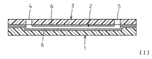
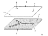
図1〜図4は本発明に係る第1の実施の形態であるマイクロ流路デバイスを示しており、図2はマイクロ流路デバイスの分解斜視図、図3は平面図であり、図1は、図3におけるI−I断面図、図4はIV−IV断面図である。
Embodiments of the present invention will be described below with reference to the drawings.
1 to 4 show a microchannel device according to a first embodiment of the present invention, FIG. 2 is an exploded perspective view of the microchannel device, FIG. 3 is a plan view, and FIG. 3 is a cross-sectional view taken along the line II in FIG. 3, and FIG. 4 is a cross-sectional view taken along the line IV-IV.
1は、プラスチック製の基板であり、例えばポリスチレン、ポリエチレン、ポリプロピレン、ポリエチレンテレフタレート、ポリエチレンナフタレート、ポリメチルメタクリレート、ポリエチレンビニルアルコール、アクリル樹脂、ポリビニル樹脂、エポキシ樹脂、ポリ塩化ビニル、不飽和ポリエステル樹脂、ポリアミド樹脂、ポリイミド樹脂、ポリスルホン樹脂、環状シクロオレフィン樹脂、セルロースアセテート、硝酸セルロース、フルオロカーボン樹脂、又はポリカーボネート等のような有機高分子材料で形成されている。基板1は、例えば一辺が数cm程度の矩形状に形成されていて、その厚みは例えば0.5mm程度である。
1 is a plastic substrate, for example, polystyrene, polyethylene, polypropylene, polyethylene terephthalate, polyethylene naphthalate, polymethyl methacrylate, polyethylene vinyl alcohol, acrylic resin, polyvinyl resin, epoxy resin, polyvinyl chloride, unsaturated polyester resin, It is made of an organic polymer material such as polyamide resin, polyimide resin, polysulfone resin, cyclic cycloolefin resin, cellulose acetate, cellulose nitrate, fluorocarbon resin, or polycarbonate. The
基板1の上面側には、微量の化学薬品や試液等のような液体を流すためのマイクロ流路2が凹んで形成されている。マイクロ流路2は、幅が例えば0.1mm程度で深さが例えば0.05mm程度の矩形状の断面形状に形成され、全体として例えば略Y字状の平面形状に形成されている。ただし、マイクロ流路2の断面形状や平面形状は、そのマイクロ流路デバイスの使用目的等に応じて、流路内部に液溜まり、ステップ、分岐、合流あるいは流路幅変更等の要素を含むものであってもよく、例えば、マイクロ流路2の断面形状は半円形等であってもよく、平面形状が略Y字状以外の形状であってもよい。
On the upper surface side of the
このようなマイクロ流路2は、例えば予めシート状に形成された基板1の素材を加熱された金型でプレス加工することにより容易に製造することができる。なお、基板1を透明な材料で形成すれば、マイクロ流路2内を外部から目視観察したり、光学的な計測や処理を行えたりする点で好ましい。また、マイクロ流路2の断面形状が半円形等であってもよい。
Such a
3は、マイクロ流路2の開放面を塞ぐために基板1の上面に接合固着される蓋板であり、基板1と同様に各種の有機高分子材料から一つを選択して形成することができる。ただし、基板1と同じ材料で形成すれば、接合や熱膨張の程度が基板1と一致する点で好ましい。また、蓋板3はガラス材料で形成してもよく、例えば珪酸ソーダガラス、硼珪酸ガラス、バリウム硼珪酸ガラス、石英ガラス等、あるいは結晶化ガラス、低融点ガラス等のようなガラス材料から選択することもできる。ただし、蓋板3側にもマイクロ流路を形成する場合には、製造コストの点でプラスチック製にした方が有利である。
蓋板3には、マイクロ流路2に連通する液体注入口4と液体排出口5とが形成されている。液体注入口4は、略Y字状に形成されたマイクロ流路2の二つの分岐流路の端部に各々面する位置に蓋板3の表裏を貫通する状態に形成され、液体排出口5は、マイクロ流路2の合流流路の端部に面する位置に蓋板3の表裏を貫通する状態に形成されている。
The
6は、基板1と蓋板3との接合、及びマイクロ流路2の内面コーティングという二つの目的に供せられる塗膜であり、有機バインダーを含有するシリカゾルを主成分とする同一の塗膜6が、この実施の形態では基板1と蓋板3の双方の対向面全面(即ち、基板1の上面と蓋板3の裏面の各全面)に塗布されて、基板1と蓋板3との接合時に加熱硬化処理されている。なお、必要な場合には、液体注入口4と液体排出口5の内周面にも塗膜6が形成される。
6 is a coating film provided for the two purposes of joining the
塗膜6の主成分であるシリカゾルは、二酸化珪素(SiO2 )の微粒子を例えばイソプロピルアルコール水溶液等のような溶媒中に分散させたもの、又は化学的に生成されたシリコンアルコキシドからなるゾルであり、溶媒を発散させるとゲル化して固形膜になる。そして、そのようなシリカゾルによって形成されたコーティング膜は有機バインダー濃度が小さい場合は親水性が大きいので、マイクロ流路2の表面に親水性が必要な場合に、親水性を得るための他の表面処理を施す必要がない。一方、コーティング膜における有機バインダー濃度が大きい場合は疎水性の膜になるので、親水性が必要な場合は親水処理をして用いる。
The silica sol as the main component of the
また、シリカゾルは耐薬性と耐熱性に優れていて、溶剤等が溶け出すことなくプラスチック材に対し強接合され、接着性の低いポリエチレン樹脂系の材料に対しても強固に接合される。ポリエチレン樹脂系の材料は、再生処理や廃棄処理に際して公害発生のおそれが少ないので、リサイクルにも使い捨て使用にも適しており、透明性があることと合わせマイクロ流路デバイスに使用するメリットが大きい。 Silica sol is excellent in chemical resistance and heat resistance, and is strongly bonded to a plastic material without dissolving a solvent or the like, and is also firmly bonded to a polyethylene resin material having low adhesion. Polyethylene resin-based materials are less likely to cause pollution during recycling and disposal, and are therefore suitable for both recycling and single use. In addition to their transparency, there are great advantages in using them for microchannel devices.
シリカゾル中に含まれる有機バインダーは、アクリル樹脂系又はエポキシ樹脂系等のように一般的な有機バインダーを用いることができ、加熱処理により発散させて任意の量だけ残すことができる。したがって、シリカゾル中への混合量と加熱処理の温度と時間等を適宜選択することにより、シリカゾル中に残る有機バインダー量を任意に制御して、例えば二酸化珪素とプラスチック材との熱膨張率の相違を緩衝する機能等を最適な状態に調整することができる。 As the organic binder contained in the silica sol, a general organic binder such as an acrylic resin type or an epoxy resin type can be used, and it can be diffused by heat treatment and left in an arbitrary amount. Therefore, the amount of organic binder remaining in the silica sol can be arbitrarily controlled by appropriately selecting the mixing amount in the silica sol, the temperature and time of the heat treatment, and the difference in thermal expansion coefficient between, for example, silicon dioxide and the plastic material. It is possible to adjust the function for buffering to an optimal state.
このような有機バインダーを含有するシリカゾルを主成分とする塗膜6は、前述のように基板1と蓋板3の双方の対向面全面に塗布形成されている。したがって、マイクロ流路2内においても十分に厚く(例えば100nm〜5μm程度に)形成することができ、マイクロ流路2内での化学反応等により発生した熱でプラスチック製の基板1が溶解しない耐熱性を確保することができる。
The
基板1と蓋板3の各対向面への塗膜6の塗布は、ディッピング、スピンコーティング又は印刷等の手段により所定の膜厚で行うことができる。膜厚は、シリカゾルの粘度、即ちゾル中の固形成分の量や有機バインダーの量等で調整することができる。なお、塗膜6の塗布は、基板1や蓋板3を所定のサイズに切断する前又は後のどちらで行ってもよい。
Application of the
基板1と蓋板3の各々に塗布された塗膜6は、基板1と蓋板3を接合する前に、例えば70℃程度の温度で30秒〜2分程度仮焼成し、有機バインダーを少し発散させて軽く硬化させるとよい。疎水処理又は特別な親水処理等が必要な場合には、この段階で印刷又はディスペンサー等を用いて処理を行う。
The
そして最後に、基板1に塗布された塗膜6と蓋板3に塗布された塗膜6とを密着させ、例えば80〜260℃程度(基板1と蓋板3の材料の選択により異なる)に加熱して塗膜6どうしを圧着させる。そのような熱圧着は、加熱ローラーやスタンパー等を用いて圧接状態で行うとよい。このようにして、基板1と蓋板3の双方の対向面に塗布された塗膜6どうしが結合して、基板1と蓋板3とが強固に接合された状態になり、同時にマイクロ流路2の内面への厚いコーティングが完了し、マイクロ流路デバイスを極めて低コストに製造することができる。
Finally, the
図5と図6は本発明に係る第2の実施の形態であるマイクロ流路デバイスを示しており、図5は平面図、図6は、図5におけるVI−VI断面図である。この実施の形態においては、電極として機能する電気配線7が基板1の上面に設けられている。基板1、マイクロ流路2及び蓋板3自体の構成は前述した第1の実施の形態に係るマイクロ流路デバイスと同様である。なお、蓋板3側に電気配線7を設けてもよい。
5 and 6 show a microchannel device according to a second embodiment of the present invention. FIG. 5 is a plan view, and FIG. 6 is a sectional view taken along line VI-VI in FIG. In this embodiment, an
電気配線7は、図5に示されるようにマイクロ流路2と交差する二箇所に互いの間に間隔をあけて配置され、各電気配線7が、図6に示されるようにマイクロ流路2の底面に面する状態に配置されている。電気配線7は、塗膜6の表裏どちら側に配置してもよいが、この実施の形態のように塗膜6の裏側に配置して、電気配線7がマイクロ流路2内に露出しないようにすれば、電気配線7がマイクロ流路2内の液体により腐食されるおそれがない点で好ましい。
As shown in FIG. 5, the
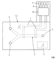
図5に示されるように、基板1から外方に突出して設けられた配線基板(リードフレーム)8には、電気配線7と電気的に導通する接続端子9が設けられていて、電気配線7を外部の測定機器等に接続することができる。ただし、接続端子9に代えてコンタクトホールやコネクター等を設けてもよい。なお、図7に示される第3の実施の形態に係るマイクロ流路デバイスのように、電気配線7を電極として駆動するための駆動IC10(例えば、交流周波数を制御する)を配線基板8に設けてもよい。また、いわゆる電子タグ11を基板1又は蓋板3内に埋設又は貼着して、来歴情報等を記録できるようにしてもよい。
As shown in FIG. 5, a wiring board (lead frame) 8 provided so as to protrude outward from the
図8は、本発明に係る第4の実施の形態であるマイクロ流路デバイスを示しており、前述した第1の実施の形態に係るマイクロ流路デバイスと同様に構成されたマイクロ流路2の途中に疎水領域12を形成したものである。具体的には、その部分だけ塗膜6を塗布せずにプラスチック材の基板1が露出するようにすればその領域が疎水領域12になる。このように、塗膜6は必ずしも基板1と蓋板3の各対向面全面に設けなくてもよい。ただし、塗膜6の一部分に対して疎水処理を施してもよいことはいうまでもない。
FIG. 8 shows a microchannel device according to a fourth embodiment of the present invention, and shows a
図9は、本発明に係る第5の実施の形態を示しており、基板1が全体にシート材で形成されて、マイクロ流路2が形成されている部分では基板1が裏面側に突出する状態になっているものである。マイクロ流路2は、角部に丸みのついた略半円状の断面形状になっている。基板1としてポリエチレン樹脂系の材料やフレキシブル基板を用いる場合等には、このような構成を採ることでマイクロ流路2を容易に低コストで形成することができる。
FIG. 9 shows a fifth embodiment according to the present invention, in which the
1 基板
2 マイクロ流路
3 蓋板
4 液体注入口
5 液体排出口
6 塗膜
7 電気配線
10 駆動IC
11 電子タグ
DESCRIPTION OF
11 Electronic tag
Claims (8)
上記基板と上記蓋板との接合、及び上記マイクロ流路の内面の全部又は一部に対するコーティングが共に、有機バインダーを含有するシリカゾルを主成分とする塗膜で行われていることを特徴とするマイクロ流路デバイス。 A plastic substrate in which a microchannel for flowing a small amount of liquid is recessed is formed with a liquid inlet and a liquid outlet that close the open surface of the microchannel and communicate with the microchannel. In the microchannel device having a configuration in which the lid plate is joined,
The bonding between the substrate and the cover plate and the coating on all or a part of the inner surface of the microchannel are both performed with a coating film mainly composed of silica sol containing an organic binder. Microchannel device.
Priority Applications (1)
| Application Number | Priority Date | Filing Date | Title |
|---|---|---|---|
| JP2007130005A JP2008284626A (en) | 2007-05-16 | 2007-05-16 | Micro-flow channel device |
Applications Claiming Priority (1)
| Application Number | Priority Date | Filing Date | Title |
|---|---|---|---|
| JP2007130005A JP2008284626A (en) | 2007-05-16 | 2007-05-16 | Micro-flow channel device |
Publications (2)
| Publication Number | Publication Date |
|---|---|
| JP2008284626A true JP2008284626A (en) | 2008-11-27 |
| JP2008284626A5 JP2008284626A5 (en) | 2010-02-18 |
Family
ID=40144841
Family Applications (1)
| Application Number | Title | Priority Date | Filing Date |
|---|---|---|---|
| JP2007130005A Pending JP2008284626A (en) | 2007-05-16 | 2007-05-16 | Micro-flow channel device |
Country Status (1)
| Country | Link |
|---|---|
| JP (1) | JP2008284626A (en) |
Cited By (10)
| Publication number | Priority date | Publication date | Assignee | Title |
|---|---|---|---|---|
| JP2011515236A (en) * | 2008-03-28 | 2011-05-19 | プレジデント アンド フェローズ オブ ハーバード カレッジ | Surface comprising microfluidic channels with controlled wetting properties |
| JP2011524815A (en) * | 2008-06-02 | 2011-09-08 | ベーリンガー インゲルハイム マイクロパーツ ゲゼルシャフト ミット ベシュレンクテル ハフツング | Microfluidic foil structure for fluid metering |
| JP2011214996A (en) * | 2010-03-31 | 2011-10-27 | Enplas Corp | Microchannel chip and microanalysis system |
| KR101191881B1 (en) | 2010-02-26 | 2012-10-16 | 한국에너지기술연구원 | protection layer of micro channel reactor and preparation method thereof |
| JP2014030382A (en) * | 2012-08-03 | 2014-02-20 | Univ Of Tokyo | Microfluidic device and method for forming lipid bilayer membrane |
| WO2014087923A1 (en) * | 2012-12-07 | 2014-06-12 | アルプス電気株式会社 | Bonded member and method for producing bonded member |
| US8883291B2 (en) | 2007-08-07 | 2014-11-11 | President And Fellows Of Harvard College | Metal oxide coating on surfaces |
| WO2015159532A1 (en) * | 2014-04-15 | 2015-10-22 | セイコーエプソン株式会社 | Chemical synthesis apparatus, and method for manufacturing chemical synthesis apparatus |
| WO2017179353A1 (en) * | 2016-04-12 | 2017-10-19 | 株式会社日立製作所 | Microreactor, formed product manufacturing system, and microreactor manufacturing method |
| WO2022181554A1 (en) * | 2021-02-25 | 2022-09-01 | キヤノン株式会社 | Microchannel device and method for manufacturing same |
Citations (15)
| Publication number | Priority date | Publication date | Assignee | Title |
|---|---|---|---|---|
| JPS62265130A (en) * | 1986-05-14 | 1987-11-18 | Hitachi Chem Co Ltd | Production of silica glass |
| JP2002518202A (en) * | 1998-06-18 | 2002-06-25 | スリーエム イノベイティブ プロパティズ カンパニー | Microfluidic product and method for producing the same |
| JP2003230829A (en) * | 2001-12-06 | 2003-08-19 | Hitachi Ltd | Plane microfactory |
| JP2004074339A (en) * | 2002-08-15 | 2004-03-11 | Fuji Electric Holdings Co Ltd | Micro-channel chip |
| JP2004516127A (en) * | 2000-06-28 | 2004-06-03 | スリーエム イノベイティブ プロパティズ カンパニー | Sample processing equipment and carrier |
| JP2005037368A (en) * | 2003-05-12 | 2005-02-10 | Yokogawa Electric Corp | Cartridge for chemical reaction, its manufacturing method, and driving system for cartridge for chemical reaction |
| JP2005103423A (en) * | 2003-09-30 | 2005-04-21 | Fuji Kagaku Kk | Microchemistry device |
| JP2005114414A (en) * | 2003-10-03 | 2005-04-28 | Univ Waseda | Flow cell |
| JP2005517959A (en) * | 2002-02-21 | 2005-06-16 | コミツサリア タ レネルジー アトミーク | Components for biological or biochemical analytical microsystems |
| JP2005257283A (en) * | 2004-03-09 | 2005-09-22 | Fluidware Technologies Kk | Microchip |
| JP2006184010A (en) * | 2004-12-24 | 2006-07-13 | Kobe Steel Ltd | Microfluid device, manufacturing method thereof, and chemical analysis device provided with microfluid device |
| JP2007063055A (en) * | 2005-08-30 | 2007-03-15 | Hiroyuki Masaki | Glass joint structure, article having glass joint structure, and method for joining glass |
| JP2007075950A (en) * | 2005-09-14 | 2007-03-29 | Kobe Steel Ltd | Micro fluid device and process of manufacture thereof |
| WO2007046484A1 (en) * | 2005-10-19 | 2007-04-26 | Sharp Kabushiki Kaisha | Electrophoretic chip, electrophoretic device, and electrophoretic system |
| WO2008065868A1 (en) * | 2006-12-01 | 2008-06-05 | Konica Minolta Opto, Inc. | Microchip substrate bonding method and microchip |
-
2007
- 2007-05-16 JP JP2007130005A patent/JP2008284626A/en active Pending
Patent Citations (15)
| Publication number | Priority date | Publication date | Assignee | Title |
|---|---|---|---|---|
| JPS62265130A (en) * | 1986-05-14 | 1987-11-18 | Hitachi Chem Co Ltd | Production of silica glass |
| JP2002518202A (en) * | 1998-06-18 | 2002-06-25 | スリーエム イノベイティブ プロパティズ カンパニー | Microfluidic product and method for producing the same |
| JP2004516127A (en) * | 2000-06-28 | 2004-06-03 | スリーエム イノベイティブ プロパティズ カンパニー | Sample processing equipment and carrier |
| JP2003230829A (en) * | 2001-12-06 | 2003-08-19 | Hitachi Ltd | Plane microfactory |
| JP2005517959A (en) * | 2002-02-21 | 2005-06-16 | コミツサリア タ レネルジー アトミーク | Components for biological or biochemical analytical microsystems |
| JP2004074339A (en) * | 2002-08-15 | 2004-03-11 | Fuji Electric Holdings Co Ltd | Micro-channel chip |
| JP2005037368A (en) * | 2003-05-12 | 2005-02-10 | Yokogawa Electric Corp | Cartridge for chemical reaction, its manufacturing method, and driving system for cartridge for chemical reaction |
| JP2005103423A (en) * | 2003-09-30 | 2005-04-21 | Fuji Kagaku Kk | Microchemistry device |
| JP2005114414A (en) * | 2003-10-03 | 2005-04-28 | Univ Waseda | Flow cell |
| JP2005257283A (en) * | 2004-03-09 | 2005-09-22 | Fluidware Technologies Kk | Microchip |
| JP2006184010A (en) * | 2004-12-24 | 2006-07-13 | Kobe Steel Ltd | Microfluid device, manufacturing method thereof, and chemical analysis device provided with microfluid device |
| JP2007063055A (en) * | 2005-08-30 | 2007-03-15 | Hiroyuki Masaki | Glass joint structure, article having glass joint structure, and method for joining glass |
| JP2007075950A (en) * | 2005-09-14 | 2007-03-29 | Kobe Steel Ltd | Micro fluid device and process of manufacture thereof |
| WO2007046484A1 (en) * | 2005-10-19 | 2007-04-26 | Sharp Kabushiki Kaisha | Electrophoretic chip, electrophoretic device, and electrophoretic system |
| WO2008065868A1 (en) * | 2006-12-01 | 2008-06-05 | Konica Minolta Opto, Inc. | Microchip substrate bonding method and microchip |
Cited By (13)
| Publication number | Priority date | Publication date | Assignee | Title |
|---|---|---|---|---|
| US8883291B2 (en) | 2007-08-07 | 2014-11-11 | President And Fellows Of Harvard College | Metal oxide coating on surfaces |
| US8802027B2 (en) | 2008-03-28 | 2014-08-12 | President And Fellows Of Harvard College | Surfaces, including microfluidic channels, with controlled wetting properties |
| JP2011515236A (en) * | 2008-03-28 | 2011-05-19 | プレジデント アンド フェローズ オブ ハーバード カレッジ | Surface comprising microfluidic channels with controlled wetting properties |
| JP2011524815A (en) * | 2008-06-02 | 2011-09-08 | ベーリンガー インゲルハイム マイクロパーツ ゲゼルシャフト ミット ベシュレンクテル ハフツング | Microfluidic foil structure for fluid metering |
| KR101191881B1 (en) | 2010-02-26 | 2012-10-16 | 한국에너지기술연구원 | protection layer of micro channel reactor and preparation method thereof |
| JP2011214996A (en) * | 2010-03-31 | 2011-10-27 | Enplas Corp | Microchannel chip and microanalysis system |
| JP2014030382A (en) * | 2012-08-03 | 2014-02-20 | Univ Of Tokyo | Microfluidic device and method for forming lipid bilayer membrane |
| WO2014087923A1 (en) * | 2012-12-07 | 2014-06-12 | アルプス電気株式会社 | Bonded member and method for producing bonded member |
| WO2015159532A1 (en) * | 2014-04-15 | 2015-10-22 | セイコーエプソン株式会社 | Chemical synthesis apparatus, and method for manufacturing chemical synthesis apparatus |
| WO2017179353A1 (en) * | 2016-04-12 | 2017-10-19 | 株式会社日立製作所 | Microreactor, formed product manufacturing system, and microreactor manufacturing method |
| JP2017189729A (en) * | 2016-04-12 | 2017-10-19 | 株式会社日立製作所 | Microreactor, chemical product production system and method for producing microreactor |
| US10464039B2 (en) | 2016-04-12 | 2019-11-05 | Hitachi, Ltd. | Microreactor, chemical product manufacturing system and microreactor manufacturing method |
| WO2022181554A1 (en) * | 2021-02-25 | 2022-09-01 | キヤノン株式会社 | Microchannel device and method for manufacturing same |
Similar Documents
| Publication | Publication Date | Title |
|---|---|---|
| JP2008284626A (en) | Micro-flow channel device | |
| KR100998535B1 (en) | Microfluidic circuit element comprising microfluidic channel with nano interstices and fabrication thereof | |
| EP1950569A1 (en) | Flow cell and process for producing the same | |
| Kelly et al. | Thermal bonding of polymeric capillary electrophoresis microdevices in water | |
| DK2394156T3 (en) | Device and method for electrochemical measurement of biochemical reactions as well as method of preparation for the device. | |
| WO2001026812A1 (en) | Microfluidic structures and methods of fabrication | |
| WO2013118447A1 (en) | Fluid handling apparatus and method for manufacturing same | |
| JP2007136292A (en) | Manufacturing method of microchannel structure, microchannel structure, and microreactor | |
| JP2008224431A (en) | Method of manufacturing microchip, and microchip | |
| JP5948248B2 (en) | Microchip and method for manufacturing microchip | |
| CN109701674A (en) | Micro-fluidic chip microelectrode technique | |
| WO2016092973A1 (en) | Fluid handling device and method for manufacturing fluid handling device | |
| JP2012225827A (en) | Fluid handling device and fluid handling system | |
| JP2004340758A (en) | Micro-fine flow passage, and micro chemical chip containing the same | |
| JP2001183291A (en) | Measurement chamber having fluorescent sensor element | |
| EP2083949A1 (en) | Method of bonding a micrifluidic device and a microfluidic device | |
| JP6549355B2 (en) | Fluid handling device | |
| JP2013010076A (en) | Method for manufacturing microchannel device and microchannel chip | |
| JP5471989B2 (en) | Biochemical reaction chip and manufacturing method thereof | |
| JP5239871B2 (en) | Microchip and manufacturing method of microchip | |
| JP4992123B2 (en) | Microchip substrate bonding method and microchip | |
| WO2009125757A1 (en) | Microchip and method for manufacturing microchip | |
| JPWO2010016370A1 (en) | Microchip, microchip manufacturing method, and microchip manufacturing apparatus | |
| JP2008304352A (en) | Channel device and method for bonding channel device-use board | |
| JP2006133003A (en) | Microchemical device and its manufacturing method |
Legal Events
| Date | Code | Title | Description |
|---|---|---|---|
| A521 | Written amendment |
Free format text: JAPANESE INTERMEDIATE CODE: A523 Effective date: 20091222 |
|
| A621 | Written request for application examination |
Free format text: JAPANESE INTERMEDIATE CODE: A621 Effective date: 20091222 |
|
| A131 | Notification of reasons for refusal |
Free format text: JAPANESE INTERMEDIATE CODE: A131 Effective date: 20120404 |
|
| RD03 | Notification of appointment of power of attorney |
Free format text: JAPANESE INTERMEDIATE CODE: A7423 Effective date: 20120420 |
|
| RD04 | Notification of resignation of power of attorney |
Free format text: JAPANESE INTERMEDIATE CODE: A7424 Effective date: 20120420 |
|
| A02 | Decision of refusal |
Free format text: JAPANESE INTERMEDIATE CODE: A02 Effective date: 20121002 |