WO2025135022A1 - 制御装置 - Google Patents
制御装置 Download PDFInfo
- Publication number
- WO2025135022A1 WO2025135022A1 PCT/JP2024/044567 JP2024044567W WO2025135022A1 WO 2025135022 A1 WO2025135022 A1 WO 2025135022A1 JP 2024044567 W JP2024044567 W JP 2024044567W WO 2025135022 A1 WO2025135022 A1 WO 2025135022A1
- Authority
- WO
- WIPO (PCT)
- Prior art keywords
- clock
- power supply
- driver
- control unit
- control
- Prior art date
- Legal status (The legal status is an assumption and is not a legal conclusion. Google has not performed a legal analysis and makes no representation as to the accuracy of the status listed.)
- Pending
Links
Images





















Classifications
-
- H—ELECTRICITY
- H02—GENERATION; CONVERSION OR DISTRIBUTION OF ELECTRIC POWER
- H02M—APPARATUS FOR CONVERSION BETWEEN AC AND AC, BETWEEN AC AND DC, OR BETWEEN DC AND DC, AND FOR USE WITH MAINS OR SIMILAR POWER SUPPLY SYSTEMS; CONVERSION OF DC OR AC INPUT POWER INTO SURGE OUTPUT POWER; CONTROL OR REGULATION THEREOF
- H02M7/00—Conversion of AC power input into DC power output; Conversion of DC power input into AC power output
- H02M7/42—Conversion of DC power input into AC power output without possibility of reversal
- H02M7/44—Conversion of DC power input into AC power output without possibility of reversal by static converters
- H02M7/48—Conversion of DC power input into AC power output without possibility of reversal by static converters using discharge tubes with control electrode or semiconductor devices with control electrode
-
- H—ELECTRICITY
- H02—GENERATION; CONVERSION OR DISTRIBUTION OF ELECTRIC POWER
- H02P—CONTROL OR REGULATION OF ELECTRIC MOTORS, ELECTRIC GENERATORS OR DYNAMO-ELECTRIC CONVERTERS; CONTROLLING TRANSFORMERS, REACTORS OR CHOKE COILS
- H02P27/00—Arrangements or methods for the control of AC motors characterised by the kind of supply voltage
- H02P27/04—Arrangements or methods for the control of AC motors characterised by the kind of supply voltage using variable-frequency supply voltage, e.g. inverter or converter supply voltage
- H02P27/06—Arrangements or methods for the control of AC motors characterised by the kind of supply voltage using variable-frequency supply voltage, e.g. inverter or converter supply voltage using DC to AC converters or inverters
Definitions
- This disclosure relates to a control device.
- Patent Document 1 a two-system configuration is provided in which an inverter circuit and a control unit are provided corresponding to the motor windings.
- Patent Document 1 if a further failure occurs while control is continuing after one failure has occurred, there is a risk that the motor drive cannot be continued.
- the purpose of this disclosure is to provide a control device that can continue abnormality monitoring and the operation of the controlled object even when an abnormality occurs.
- the control device of the present disclosure includes a control unit, a power source, and a clock source.
- the control unit has an arithmetic circuit that performs control calculations.
- the power source supplies power to the control unit.
- the clock source supplies a clock for the control calculation in the arithmetic circuit.
- At least one of the arithmetic circuits, power sources, and clock sources has a redundant configuration of three or more. If an abnormality occurs in a location that is redundant with three or more, the abnormal location is identified and abnormality monitoring and operation can be continued using two or more normal sources. By having redundancy with three or more, even if an abnormality occurs in one location, abnormality monitoring and operation of the controlled object can be continued as long as two or more configurations are normal.
- FIG. 1 is a schematic diagram showing an electric power steering device according to a first embodiment.
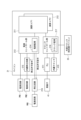
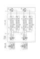
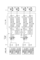
- FIG. 2 is a block diagram showing an ECU according to a first embodiment;
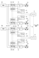
- FIG. 3 is a circuit diagram illustrating a driver circuit according to a first embodiment;
- FIG. 4 is a circuit diagram illustrating a driver component according to a first embodiment;
- FIG. 5 is a circuit diagram illustrating a driver component according to a first embodiment;
- FIG. 6 is a circuit diagram illustrating a driver component according to a first embodiment;
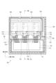
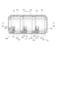
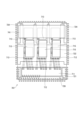
- FIG. 7 is a plan view showing the driver components according to the first embodiment;
- FIG. 1 is a schematic diagram showing an electric power steering device according to a first embodiment.
- FIG. 2 is a block diagram showing an ECU according to a first embodiment;
- FIG. 3 is a circuit diagram illustrating a driver circuit according to a first embodiment;
- FIG. 4 is a circuit diagram illustrating a driver component according to a first embodiment;
- FIG. 5 is a circuit diagram
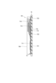
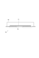
- FIG. 8 is a cross-sectional view taken along line VIII-VIII in FIG. 7;
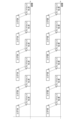
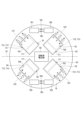
- FIG. 9 is a schematic diagram illustrating a substrate arrangement according to the first embodiment;
- FIG. 10 is a schematic diagram illustrating a substrate arrangement according to the first embodiment;
- FIG. 11 is a schematic diagram illustrating a substrate arrangement according to the first embodiment;
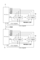
- FIG. 12 is an explanatory diagram for explaining the connection between the microcomputer and the components in two systems.
- FIG. 13 is an explanatory diagram for explaining the connection between the microcomputer and the components in three systems.
- FIG. 14A is an explanatory diagram showing an inter-system connection line according to the first embodiment;
- FIG. 14B is an explanatory diagram showing an inter-system connection line according to the first embodiment;
- FIG. 14A is an explanatory diagram showing an inter-system connection line according to the first embodiment;
- FIG. 14B is an explanatory diagram showing an inter-system connection line according to the first embodiment;
- FIG. 14A is an explanatory diagram showing
- FIG. 15 is an explanatory diagram showing an isolator according to a first embodiment
- FIG. 16 is an explanatory diagram illustrating a communication configuration between a microcomputer and a driver component according to the first embodiment
- FIG. 17 is an explanatory diagram illustrating a communication configuration between a microcomputer and a driver component according to the first embodiment
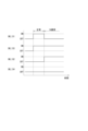
- FIG. 18 is a time chart illustrating data communication according to the first embodiment
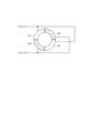
- FIG. 19 is a schematic diagram showing an arrangement in which a motor winding is provided in two systems
- FIG. 20 is a schematic diagram showing an arrangement of four motor windings
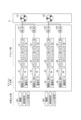
- FIG. 21 is a time chart illustrating communication between the arithmetic core and the pre-driver IC according to the first embodiment
- FIG. 22 is a time chart for explaining communication with the pre-driver IC when some of the arithmetic cores fail according to the first embodiment;
- FIG. 23 is an explanatory diagram illustrating an inter-system connection line according to the first embodiment;
- FIG. 24 is a block diagram illustrating the driving of the power supply relay and the reverse connection protection relay according to the first embodiment;
- FIG. 25 is a block diagram illustrating a redundant configuration in a microcomputer according to a first embodiment;
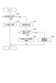
- FIG. 26 is a flowchart illustrating a clock monitoring process according to the first embodiment;
- FIG. 27 is a flowchart illustrating a power supply monitoring process according to the first embodiment.
- FIG. 28 is a block diagram illustrating the driving of a power supply relay and a reverse connection protection relay according to a second embodiment;
- FIG. 29 is a block diagram illustrating the driving of a power supply relay and a reverse connection protection relay according to a third embodiment
- FIG. 30 is a block diagram illustrating an ECU according to the first embodiment
- FIG. 31 is a block diagram illustrating an ECU according to a fourth embodiment
- FIG. 32 is a block diagram illustrating an ECU according to a fifth embodiment
- FIG. 33 is a block diagram illustrating an ECU according to a sixth embodiment
- FIG. 34 is a schematic diagram showing an arrangement of motor windings in a case where the motor windings are arranged in three systems.
- FIG. 35 is a block diagram illustrating an ECU according to a seventh embodiment
- FIG. 36 is a block diagram illustrating an ECU according to an eighth embodiment
- FIG. 37 is a block diagram illustrating an ECU according to a ninth embodiment
- FIG. 38 is a block diagram illustrating the calculation timing according to the ninth embodiment
- FIG. 39 is a block diagram illustrating an ECU according to a tenth embodiment
- FIG. 40 is a time chart illustrating the operation of the motor relay according to the tenth embodiment
- FIG. 41 is a schematic diagram illustrating a substrate arrangement according to an eleventh embodiment
- FIG. 42 is a schematic diagram illustrating a substrate arrangement according to the eleventh embodiment
- FIG. 43 is a schematic diagram illustrating a substrate arrangement according to the twelfth embodiment
- FIG. 44 is a block diagram illustrating an ECU according to a twelfth embodiment
- FIG. 45 is a block diagram illustrating an ECU according to a thirteenth embodiment
- FIG. 46 is a time chart illustrating the operation of the motor relay according to the thirteenth embodiment
- FIG. 47 is a time chart illustrating the operation of the motor relay according to the thirteenth embodiment
- FIG. 48 is a schematic diagram illustrating a substrate arrangement according to the fourteenth embodiment
- FIG. 49 is a schematic diagram illustrating a substrate arrangement according to the fifteenth embodiment
- FIG. 50 is a plan view showing a driver component according to a sixteenth embodiment
- FIG. 51 is a cross-sectional view taken along line LI-LI in FIG. 50
- FIG. 52 is a cross-sectional view taken along line LII-LII of FIG. 50;
- FIG. 53 is a plan view showing a driver component according to a seventeenth embodiment
- FIG. 54 is a cross-sectional view taken along line LIV-LIV in FIG. 53
- FIG. 55 is a cross-sectional view taken along line LV-LV in FIG. 53
- FIG. 56 is a plan view showing a driver component according to the eighteenth embodiment.
- a drive device 10 includes a motor 11 and an ECU 15 as a communication device, and is applied to, for example, an electric power steering device 5, which is a steering device for assisting the steering operation of a vehicle.
- Figure 1 shows the overall configuration of a steering system 90 including the electric power steering device 5.
- the steering system 90 includes a steering wheel 91, which is a steering member, a steering shaft 92, a pinion gear 96, a rack shaft 97, wheels 98, the electric power steering device 5, etc.
- the steering wheel 91 is connected to a steering shaft 92.
- a torque sensor 93 that detects steering torque is provided on the steering shaft 92.
- a pinion gear 96 is provided at the tip of the steering shaft 92.
- the pinion gear 96 meshes with a rack shaft 97.
- a pair of wheels 98 are connected to both ends of the rack shaft 97 via tie rods or the like.
- the steering shaft 92 connected to the steering wheel 91 rotates.
- the rotational motion of the steering shaft 92 is converted into linear motion of a rack shaft 97 by a pinion gear 96.
- a pair of wheels 98 are steered to an angle that corresponds to the amount of displacement of the rack shaft 97.
- the electric power steering device 5 includes a drive unit 10 and a reduction gear 6 as a power transmission unit that reduces the speed of the rotation of the motor 11 and transmits it to the rack shaft 97.
- the electric power steering device 5 of this embodiment is a so-called "rack assist type", but it may also be a so-called “column assist type” that transmits the rotation of the motor 11 to the steering shaft 92.
- the drive unit 10 is a so-called “mechanically and electrically integrated” type in which the ECU 15 is integrally provided on one side of the motor 11 in the axial direction.
- the ECU 15 has a connector 16, and is connected to the vehicle power supply 7, vehicle communication network 8, and torque sensor 93 via the connector 16.
- the vehicle power supply 7 includes power supplies 501 and 502, which will be described later.
- the vehicle communication network 8 is, for example, a CAN (Controller Area Network), and is indicated as "CAN" in the figure.
- the ECU 15 is disposed coaxially with the motor 11, on the opposite side to the output shaft of the motor 11.
- coaxial means that errors and misalignments related to, for example, assembly and design are allowed.
- the axial direction of the motor 11 is regarded as the axial direction of the drive unit 10, and will be referred to simply as the "axial direction.” The same applies to "radial direction” and “circumferential direction.”
- the motor 11 is, for example, a three-phase brushless motor, and has four motor windings 121 to 124.
- the motor 11 outputs all or part of the torque required for steering, and is driven by power supplied from power sources 501 and 502 to rotate the reduction gear 6 forward and reverse.
- the ECU 15 has microcomputers 21, 23, power supply ICs 31, 33, communication units 36, 38, oscillators 41, 43, driver circuits 51-54, pre-driver ICs 61-64, and position sensors 66-69. Note that the subscripts "1", “2", “1A”, “2A”, “1B”, “2B”, etc. indicate that the components are provided correspondingly, and the reference numbers are omitted as appropriate for components that can be identified by the subscripts.
- the components that make up the ECU 15 are mounted on a board 75 that is provided approximately parallel to one end face of the motor 11 in the axial direction (see Figure 1). Although one board 75 is shown in Figure 1, multiple boards may be used.
- the microcomputer 21 has arithmetic cores 211, 212 with lockstep.
- the microcomputer 23 has arithmetic cores 231, 232 with lockstep.
- the microcomputers 21, 23 are arranged so that they can send and receive information to each other through inter-microcomputer communication. In this embodiment, the microcomputers 21, 23 are configured similarly, but the performance and detailed configuration may differ. Details of the microcomputers 21, 23 will be described later.
- Microcontroller 21 receives power from power supply IC 31, and microcontroller 23 receives power from power supply IC 33.
- Power supply ICs 31 and 33 are power management ICs (PMICs).
- PMICs power management ICs
- power is supplied from power supply 501 to the components above the dashed dotted line in FIG. 2, and power is supplied from power supply 502 to the components below the dashed dotted line.
- drive device 10 in this embodiment is a "two power supply system" in which power is supplied from two power supplies 501 and 502.
- the communication units 36 and 38 are used to send and receive various information.
- the communication units 36 and 38 are connected to the vehicle communication network 8 and acquire vehicle signals from the vehicle communication network 8.
- the oscillators 41 and 43 are clock sources such as quartz crystals or ceramic oscillators.
- driver circuit 51 has six switching elements 511-516 and is provided corresponding to winding 121.
- Driver circuit 52 has six switching elements 521-526 and is provided corresponding to winding 122.
- Driver circuit 53 has six switching elements and is provided corresponding to winding 123.
- Driver circuit 54 has six switching elements and is provided corresponding to winding 124.
- Motor relays 131-134 are provided between driver circuits 51-54 and windings 121-124 (see FIG. 39).
- switching elements 511 to 513 are provided on the high potential side, and switching elements 514 to 516 are provided on the low potential side, and are bridge-connected.
- Switching elements 511 and 514 are connected to the U phase of the winding 121
- switching elements 512 and 515 are connected to the V phase of the winding 121
- switching elements 513 and 516 are connected to the W phase of the winding 121.
- switching elements 521 to 523 are provided on the high potential side, and switching elements 524 to 526 are provided on the low potential side, and are bridge-connected.
- Switching elements 521 and 524 are connected to the U phase of the winding 122
- switching elements 522 and 525 are connected to the V phase of the winding 122
- switching elements 523 and 526 are connected to the W phase of the winding 122.
- the switching element on the high potential side will be referred to as the upper arm element
- the switching element on the low potential side as the lower arm element, as appropriate.
- the switching elements in this embodiment are MOSFETs, but may also be IGBTs, bipolar transistors, etc.
- the driver circuits 51 and 52 are connected to the power supply 501. Between the power supply 501 and the driver circuit 51, there are provided a power supply relay 551, a reverse connection protection relay 556, a choke coil 562, and a capacitor 566. The choke coil 561 and the capacitor 566 form a filter circuit. Between the power supply 501 and the driver circuit 52, there are provided a power supply relay 552, a reverse connection protection relay 557, a choke coil 562, and a capacitor 567. The choke coil 562 and the capacitor 567 form a filter circuit. The driver circuits 53 and 54 are connected to the power supply 502.
- the circuit configurations of the driver circuits 53 and 54, and the power supply relay, reverse connection protection relay, and filter circuit provided between the power supply 502 and the driver circuits 53 and 54 are similar to those of the driver circuits 51 and 52, the power supply relays 551 and 552, etc., and therefore will not be described.
- pre-driver ICs 61-64 are provided corresponding to driver circuits 51-54.
- Pre-driver ICs 61 and 62 are provided to be capable of digital communication with microcomputer 21
- pre-driver ICs 63 and 64 are provided to be capable of digital communication with microcomputer 23.
- Microcomputers 21 and 23 transmit three-phase drive commands for motor 11 to each of pre-driver ICs 61-64 as a set of digital signals.
- the pre-driver IC 61 is communicatively connected to the calculation core 211
- the pre-driver IC 62 is communicatively connected to the calculation core 212
- the pre-driver IC 63 is communicatively connected to the calculation core 231
- the pre-driver IC 64 is communicatively connected to the calculation core 232.
- the communication lines connecting the pre-driver ICs 61 to 64 and the calculation cores 211, 212, 231, and 232 are connected by the system connection line 25.
- the system connection lines 25 mean that the four connection lines connecting the cores and the pre-driver ICs are connected to the same potential. Therefore, even if a line is broken at the point indicated by the arrow mid in Figure 2, it is still possible to send and receive signals between the calculation cores 1A, 1B and the pre-drivers 2A, 2B.
- An isolator 28 (not shown in FIG. 2 ), which will be described later, is provided on the inter-system connection line 25.
- the isolator 28 may be provided at any location on the inter-system connection line 25. The same effect can also be achieved by providing an isolator function to necessary components.
- Position sensors 66-69 detect the rotation of motor 11. Position sensors 66-69 are connected to calculation cores 211, 212, 231, 232, respectively. Communication lines connecting position sensors 66-69 and microcomputers 21, 23 are connected by inter-system connection line 256. Communication lines connecting power supply ICs 31, 33 and microcomputers 21, 23 are connected by inter-system connection line 257, and communication lines connecting communication units 36, 38 and microcomputers 21, 23 are connected by inter-system connection line 258. Note that inter-system connection lines 256-258 may be omitted.
- the pre-driver IC will be explained based on FIG. 4.
- the pre-driver IC 61 will be explained as a representative example.
- the pre-driver IC 61 includes a three-phase pre-driver circuit 611 that transmits gate signals to the switching elements that make up the driver circuit 51.
- the pre-driver IC 61 also includes a current detection circuit 612, a temperature detection circuit 613, an abnormality detection unit 614, and a relay driver circuit 621.
- the pre-driver circuit 611 outputs a gate signal as a drive signal to the switching elements 511-516 based on a drive command from the microcomputer 21.
- the current detection circuit 612 detects the motor current based on the detection values of the current detection elements 517-519.
- the current detection elements 517-519 are current sense MOSs, and are built into the low-side chip 713, which will be described later.
- the current sense MOSs may be built into the high-side chip 712, or may be a chip separate from the upper and lower arm elements.
- the current detection element 531 may be a shunt resistor provided in the arm of each phase.
- the shunt resistor is provided on the low potential side of the lower arm element, but it may also be provided on the high potential side of the upper arm element.
- the current detection element 532 may be a Hall element provided between the connection point of the upper and lower arm elements and the motor winding.
- the current detection elements 531, 532 are shown as being provided within the driver component 701 described below, but they may also be provided outside the driver component 701. Note that the motor relay 131 is omitted from FIG. 6.
- the temperature detection circuit 613 detects the temperatures of the driver circuit 50 and the pre-driver IC 60 itself based on the detection value of a temperature detection element (not shown).
- the abnormality detection unit 614 monitors abnormalities in the driver circuit 50 based on the gate-source potential difference and drain-source potential difference of the elements that make up the driver circuit 50, and on drive commands from the microcontroller 21. For example, the abnormality detection unit 614 monitors abnormalities such as short circuits and open terminals based on the potential difference. The abnormality detection unit 614 also monitors overheating abnormalities based on temperature information and abnormalities in the pre-driver IC 61 itself.
- the relay driver circuit 621 outputs a gate signal as a drive signal to the power supply relay 551, reverse connection protection relay 556, and motor relay 131 based on a drive command from the microcontroller 21.
- the pre-driver IC 61 transmits the current detection value, temperature information, and abnormality information to the microcomputer 21.
- Information transmission from the pre-driver IC 61 to the microcomputer 21 may be digital communication or analog communication.
- the corresponding driver circuits 51-54 and pre-driver ICs 61-64 are provided in the same package as a single driver component 701-704.
- a driver component 701 having a driver circuit 51 and a pre-driver IC 61 is illustrated.
- the sealing portion 749 is omitted in order to explain the inside of the component, and in Fig. 8, the hatching of the sealing portion 749 is omitted.
- the driver component 701 has a control chip 711, a high-side chip 712, a low-side chip 713, an intermediate clip 715, a ground clip 716, a lead frame 72, etc., and is sealed with a sealing portion 749.
- the sealing portion 749 is formed in a generally rectangular shape in a plan view, and terminals are formed along the outer edge. The terminal arrangement and shape are not important, and the terminals may be of a non-lead type, or may be formed to protrude outside the sealing portion 749.
- the driver component 701 is also provided with a temperature detection element such as a temperature sensing diode. The temperature detection element may be built into the high-side chip 712 or the low-side chip 713, similar to the current detection elements 517 to 519.
- the lead frame 72 includes a control land 721, a power land 722, an output land 723, and a ground land 724.
- the back side of the lead frame 72 is exposed from the sealing portion 749, and is electrically connected to the wiring pattern of the substrate 75 by soldering or the like. Note that not all lands need to be connected to the substrate 75 on the back side.
- the region on the control land 721 side is referred to as the IC region Ric
- the region on the power land 722 side is referred to as the drive element region Rd.
- the driver component 701 the end on the power land 722 side (upper side of the paper in FIG. 7) is referred to as the element side end, and the end on the control land 721 side (lower side of the paper in FIG. 7) is referred to as the IC side end.
- the control chip 711 constitutes the pre-driver IC 61 and is disposed on the control land 721.
- the control land 721 on which the control chip 711 is mounted is at ground potential, but if a control chip 711 with an insulated back side is used, the potential of the control land 721 may be a potential other than ground potential, such as a power supply potential.
- the control terminals which are terminals provided in the control region Rc, are connected to the microcontroller 21, the power supply IC 31, and the other pre-driver ICs 62 to 64.
- the control terminals include a clock signal terminal, a PWM frequency synchronization terminal, and a sample-and-hold terminal.
- the control terminals include a chip select terminal, a MISO terminal, a MOSI terminal, etc.
- the three high-side chips 712 each have an upper arm element for each phase built in, and the three low-side chips 713 each have a lower arm element for each phase built in.
- the low-side chip 713 also has current detection elements 517 to 519 built in.
- the three high-side chips 712 are arranged on a power land 722, which is at the power supply potential.
- the high-side chips 712 are arranged side by side along the long side of the control chip 711, with their gate electrodes facing the control chip 711.
- the source electrodes of the high-side chips 712 face upward, and the drain electrodes provided on the back side are connected to the power land 722.
- the intermediate clip 715, low-side chip 713, and ground clip 716 are layered in this order, forming a stack structure.
- the intermediate clip 715 is a conductive metal plate made of, for example, copper, and is provided for each of the three high-side chips 712.
- the lower surface of the intermediate clip 715 is connected to the source electrode of the high-side chip 712, and the upper surface is connected to the drain electrode of the low-side chip 713.
- the intermediate clip 715 is shifted to an extent that the signal line 718 can be connected on the control chip 711 side of the high-side chip 712.
- the end of the intermediate clip 715 opposite the control chip 711 is bent downward and connected to the output land 723.
- the output land 723 is connected to the motor terminal and is connected to each phase of the motor winding 121 via board wiring, etc.
- the intermediate clip 715 is spaced apart from adjacent frames in the width direction to an extent that insulation can be ensured, and is formed wider than the high-side chip 712.
- the area of the intermediate clip 715 is formed to be larger than the high-side chip 712.
- the ground clip 716 is a conductive plate made of, for example, copper, and is provided across the three low-side chips 713.
- the ground clip 716 is offset to an extent that the signal line 718 can be connected on the control chip 711 side of the low-side chip 713.
- the ground clip 716 is bent downward on one side in the width direction and connected to the ground land 724.
- the ground clip 716 is provided within the sealing portion 749, but the top surface side may be exposed from the sealing portion 749.
- the high-side chip 712 and the low-side chip 713 are connected to the control chip 711 by signal lines 718.
- the high-side chip 712 and the low-side chip 713 are stacked, but are offset and stacked in a staircase pattern to ensure a non-overlapping area that does not overlap with the components provided above, making it possible to connect the signal lines 718 in the non-overlapping area.
- the connection ends of the signal lines 718 on the control chip 711 side are concentrated on one side of the control chip 711.
- the signal lines 718 include lines for gate drive, current detection, and temperature detection. This makes it possible to separate the inside of the driver component 701 into a drive element region Rd through which a large current flows and an IC region Ric.
- Figs. 9 to 11 show the side of the board 75 facing the motor 11
- Fig. 10 shows the side of the board 75 opposite the motor 11.
- Fig. 11 shows a schematic diagram of the layout of the driver components 701 to 704 and the motor windings 121 to 124 on the board 75. The same is true for Fig. 42 etc.
- driver components 701 to 704 are mounted on a board 75.
- the four driver components 701 to 704 are provided on the surface of the board 75 facing the motor 11.
- the four driver components 701 to 704 are arranged on concentric circles at roughly equal intervals.
- Driver components 701, 702 and driver components 703, 704 are arranged symmetrically with respect to board partition line D1.
- Board partition line D1 is a partition line that separates areas with different power supplies.
- the driver components 701-704 are arranged so that the ends on the element side face radially outward.
- the motor windings 121-124 are connected to the substrate 75 on the radially outer side of the driver components 701-704. That is, from the radially inner side, they are arranged in the order of the control chip 711, the high-side chip 712, the low-side chip 713, and the motor line connection part.
- the take-out wires of the motor windings 121-124 are arranged approximately parallel to the element side ends of the driver components 701-704 so as to correspond to the phase arrangement of the switching elements in the driver components 701-704. Note that the phase arrangement shown in FIG. 11 is an example, and may be different. In FIG. 9-FIG. 11, the winding connection points to which the take-out wires of the motor windings are connected are numbered as the motor windings 121-124. The same applies to the power terminals and the signal terminals.
- a rotation detector 65 is mounted on the surface of the substrate 75 facing the motor 11, in a position opposite a magnet provided at the end of the shaft (not shown) of the motor 11. In this embodiment, the rotation detector 65 is mounted in the center of the substrate 75.
- the rotation detector 65 includes position sensors 66 to 69.
- the power terminals 761, 763 are connected to the outer edge of the board 75 in an area that straddles the board center line D2, which is perpendicular to the board partition line D1.
- the power terminals 761, 763 include a power terminal and a ground terminal.
- the power terminal 761 is supplied with power from the power source 501, and the power terminal 763 is supplied with power from the power source 502.
- the power supply ICs 31, 33 are mounted on the board 75 on the board center line D2 between the rotation detection unit 65 and the power terminals 761, 763.
- the power supply ICs 31, 33 may be located anywhere other than on the board center line D2 as long as they are easily connected to the power terminals 761, 763 and the microcomputers 21, 23.
- a signal terminal 77 is connected to the outer edge of the board 75 in an area that straddles the board partition line D1.
- microcomputers 21 and 23 are mounted on both sides of the board center line D2 on the board partition line D1.
- a wiring pattern is formed so that power is supplied to the microcomputer 21 from power terminal 761, and power is supplied to the microcomputer 23 from power terminal 763.
- the microcomputers 21 and 23 are connected so that they can communicate with each other, and an isolator 28 is mounted at the connection point between the microcomputers 21 and 23.
- the isolator 28 is provided at the center of the board.
- components such as capacitors and coils that constitute a filter circuit are mounted on the surface opposite the motor 11.
- the drive unit 10 is applied to an electric power steering device 5.
- various components may be made redundant to ensure safety even if some components fail.
- FIGS. 12 to 15 conceptually show the communication configuration between the microcontrollers and components.
- a combination of microcontrollers (or calculation cores) M1, M2 and components P1, P2 communicatively connected by communication lines C1, C2 is considered to be a control system
- the microcontroller M1 or component P1 which is the first control system
- the microcontroller M2 and component P2 which are the second control system
- control cannot continue.
- microcomputers M1 and M2 correspond to microcomputers 21 and 23, and components P1 and P2 correspond to driver components 701 and 703.
- Driver components 701 and 703 include pre-driver ICs 61 and 63 that control driver circuits 51 and 53, and output drive signals that drive driver circuits 51 and 53 in response to commands sent from microcomputers 21 and 23.
- driver components 701 and 703 send current detection values, driver outputs, abnormality information, temperature information, etc. to microcomputers 21 and 23.
- the driver components 701 and 703 are capable of digital communication, the first communication line C1 and the second communication line C2 are connected by an inter-system connection line 25.
- the microcomputer 23 issues a command to the driver components 701 and 703. This allows control to continue.
- the second failure occurs in either the driver component 701 or 703, control can be continued with a normal microcomputer and driver component. This increases the possibility of continued operation in the event of a failure, even with two control systems.
- the driver components 701 and 703 may be connected by an inter-system connection line 25.
- the communication between the microcontrollers 21, 23 and the components 701, 703 is, for example, SPI communication, but it may be a communication method other than SPI, such as PSI5, SENT, CAN, Ethernet, Flexray, etc., or it may be wireless communication. Also, in FIG. 14 etc., one communication line is shown, but the number of communication lines and the number of terminals can be set arbitrarily depending on the communication method, etc.
- an isolator 28 is provided as a system separation component in a location where simultaneous failures are undesirable. Note that the illustration of the isolator 28 has been omitted from FIG. 2 and other figures.
- the isolator 28 is provided in the inter-system connection line 25, but it may also be provided, for example, inside the microcontrollers M1 and M2 or the components P1 and P2. Any configuration that can transmit information while maintaining a potential difference is sufficient for separating the systems, and the system separation component may be provided with a passive blocking component such as a resistor or a buffer instead of an isolator. Also, simultaneous failures may be prevented by using wireless communication for communication.
- microcontrollers 21 and 23 can transmit a common clock signal SCLK and a MOSI signal to corresponding driver components 701 to 704, and can transmit a chip select signal CS_A to driver components 701 and 703, and a chip select signal CS_B to driver components 702 and 704.
- driver components 701 to 704 can transmit a MISO signal to the corresponding microcontrollers 21 and 23.
- the microcontrollers 21 and 23 are set up to be able to communicate with each other, and perform PWM synchronization, duty update timing synchronization, and sample hold timing synchronization for the four driver components 701-704.
- the microcontrollers 21 and 23 use the MISO signal to check the PWM update using the PWM reflected value and current detection value.
- PWM update check may be performed by configuring the driver components 701-704 to return the driver output to the microcontrollers 21 and 23. If the driver output is not returned to the microcontrollers 21 and 23, the terminals and wiring for returning the driver output can be omitted.
- driver component 701, and driver component 702 may be connected in a so-called "daisy chain" configuration, in which communication lines are connected in a circular fashion.
- the microcomputer 23, driver component 703, and driver component 704 may be connected in a daisy chain.
- signals from the microcontrollers 21 and 23 are sent to driver components 701 and 703, and the signals are then sent from the driver components 701 and 703 to the driver components 702 and 704.
- the driver components 702 and 704 then send MISO signals to the microcontrollers 21 and 23, and so on.
- the chip select signal and sample and hold may be shared. This makes it possible to reduce the number of terminals and wiring.
- the microcomputers 21 and 23 since the communication lines of each control system are connected by the inter-system connection lines 25, in order to prevent data from being mixed on the communication lines, the microcomputers 21 and 23 will not issue commands when communication from another microcomputer begins, or will output commands a predetermined time after a response from the driver components 701 and 703.
- the destination of commands from the microcomputers 21 and 23 may be specified by chip select, ID assignment, etc.
- FIG. 18 explains an example of data transmission and reception.
- the microcontrollers 21, 23 output an ID and a command to specify the part to be driven.
- the part to be driven is specified by the ID, and a current command value and on-duty are transmitted to the part side by MOSI.
- the ID method the part to be driven is specified by the ID, but it is also possible to set an ID that commands multiple parts simultaneously. This makes it possible, for example, to align the timing of current detection for multiple parts.
- the part to be driven may be specified by the chip select method.
- Driver components 701 and 703 transmit current values and status information to microcontrollers 21 and 23.
- Data transmission from driver components 701 and 703 is performed by MISO, so information can be transmitted even while commands are being transmitted from microcontrollers 21 and 23.
- transmission from driver component 703 is set to start when transmission from driver component 701 is completed.
- Data arbitration can also be performed by setting transmission to be in ID order, for example.
- Figures 19 and 20 show schematic layouts of motor windings, with three-phase wiring depicted as a single line.
- the stator has multiple windings, which are connected to form a three-phase motor with three input terminals.
- Figure 19 shows an example of configuring two sets of three-phase windings; when connecting windings that are 180° apart, the wiring for connecting the multiple windings and the configuration of the busbars that carry the wiring tend to become complicated.
- the board 75 is provided on one side of the motor 11 in the axial direction, and the components corresponding to each power source are concentrated and arranged in an area defined by the board partition line D1 (see Figures 1, 9 to 11).
- the four motor windings 121-124 are assigned to the two power sources 501, 502 and the two microcomputers 21, 23. When the motor 11 is driven by the four motor windings 121-124, the winding sets that are 180° opposed to each other are often driven in the same phase.
- windings with different drive phases that are arranged next to each other on the stator are assigned to one power supply system. Specifically, power is supplied to windings 121 and 122 from power supply 501, and power is supplied to windings 123 and 124 from power supply 502.
- one core can also output commands to windings assigned to other power supplies. Therefore, even if two windings with different drive phases that are arranged next to each other on the stator are assigned to the same power supply, drivers that are driven in the same phase can be operated by commands from the same core.
- the timing at which the current draw reaches its maximum when the motor is driven shifts. This makes it possible to smooth out the power consumption in the driver circuit, and for example to make the smoothing capacitor smaller, compared to when driver circuits driven in the same phase are assigned to the same power supply. It is also possible to consolidate components assigned to the same power supply system on one side of the board, improving layout, and reducing the occurrence of common cause failures due to wiring shorts.
- windings 121 and 123 that are energized in the same phase are shown in white, and windings 122 and 124 that are energized in the same phase but in a different phase from windings 121 and 123 are shown in matte finish.
- calculation core 211 will be referred to as "core 1A”, the calculation core 212 as “core 1B”, the calculation core 231 as “core 2A”, the calculation core 232 as “core 2B”, the pre-driver IC 61 as "pre-driver 1A”, the pre-driver IC 62 as “pre-driver 1B”, the pre-driver IC 63 as "pre-driver 2A”, and the pre-driver IC 64 as "pre-driver 2B".
- windings 121, 123 provided for pre-drivers 1A, 2A are wound around the stator in opposing directions and energized in the same phase.
- Windings 122, 124 provided for pre-drivers 1B, 2B are wound around the stator in opposing directions and energized in the same phase.
- the energization phase of windings 121, 123 is different from the energization phase of windings 122, 124.
- the amplitude of the currents flowing through windings 121 to 124 is assumed to be equal.
- cores 1A and 2A transmit command signals such as duty command values and various drive permission signals to pre-drivers 1A and 2A, which are driven in the same phase.
- Pre-drivers 1A and 2A transmit current detection values and status information (e.g., driver output, abnormality information, temperature information, etc.) to cores 1A and 2A.
- Cores 1B and 2B transmit command signals such as duty command values and various drive permission signals to pre-drivers 1B and 2B, which are driven in the same phase.
- Pre-drivers 1B and 2B transmit current detection values and status information to cores 1B and 2B.
- cores 1A and 2A send drive commands to pre-drivers 1A and 2A, but do not send drive commands to pre-drivers 1B and 2B.
- the pre-drivers 1B and 2B may be configured to send current detection values and status information to cores 1A and 2A that have not received a drive command.
- the pre-drivers 1A and 2A may be configured to send current detection values and status information to cores 1B and 2B that have not received a drive command. This allows each core to grasp the control state of the entire drive device 10.
- Cores 1A and 2A alternately send commands to pre-drivers 1A and 2A.
- cores 1B and 2B alternately send commands to pre-drivers 1B and 2B. This makes it possible to reduce the computational load on each core.
- the command may be sent from the normal core 1A instead of the core 2A. This makes it possible to prevent performance degradation, including the update cycle. Also, the pre-drivers 1B and 2B that do not use the command from the core 2A can continue to perform control without being affected by the failure of the core 2A.
- the system connection line 25 may be divided between group A and group B, which are driven in the same phase.
- the system connection line for group A is "25A”
- the system connection line for group B is "25B”.
- the power relays 551-554 and reverse connection protection relays 556-559 are provided for each driver circuit 51-54, and are driven in normal operation by receiving individual commands from the relay driver circuits 621-624 of the corresponding driver circuits 51-54.
- the power relays and reverse connection protection relays are collectively referred to as "power supply/reverse connection relays", and the calculation core in the microcomputer is omitted.
- the inter-system connection lines are shown as being separate for group A and group B as in FIG. 23, but the inter-system connection lines may be grouped together as in FIG. 2.
- the pre-driver IC 61 If an abnormality occurs in the pre-driver IC 61, power relay 551, or reverse connection protection relay 556, the pre-driver IC 61 is configured to be pulled down (off), and the other pre-driver ICs 62 to 64 are not driven. The same applies if an abnormality occurs in the other pre-driver ICs, power relays, reverse connection protection relays, or motor relays (not shown in FIG. 24).
- the microcomputer 23 issues a command to the relay driver circuits 621, 622 in the pre-driver ICs 61, 62 to drive the power relays 551, 552 and the reverse connection protection relays 556, 557.
- the microcomputer 21 issues a command to the relay driver circuits 623, 624 in the pre-driver ICs 63, 64 to drive the power relays 553, 554 and the reverse connection protection relays 558, 559.
- the motor 11 can continue to be driven by driving the relays with a command from the other microcomputer.
- the microcomputer 21 has arithmetic cores 211 and 212, a power supply control unit 213, and a clock control unit 217.
- the power supply control unit 213 has a power supply monitoring unit 214.
- the power supply control unit 213 is connected to a plurality of power supply circuits PM1 to PM3.
- the power supply circuits PM1 and PM2 correspond to the power supply IC 31, and the power supply circuit PM3 corresponds to the power supply IC 33.
- the power supply IC 31 has, for example, a core power supply voltage output (e.g., about 1.2 [V]) and a power supply output different from the core power supply voltage (e.g., 5 [V]), with the core power supply corresponding to the power supply circuit PM1 and the 5V power supply corresponding to the power supply circuit PM2.
- the power supply circuits PM1 and PM2 correspond to the same power supply IC 31, but generate different voltages inside the power supply IC 31, and can be considered as "different power supply sources.”
- the power supply control unit 213 of this embodiment can be said to have a redundant configuration in which power is supplied from three different power supply sources.
- the power supply circuit PM1 is input to the power supply control unit 213 at its original voltage and used by the arithmetic cores 211 and 212.
- the power from the power supply circuit PM2 is stepped down by an internal step-down circuit 215 and input to the power supply control unit 213 for use in the core arithmetic.
- the power from the power supply circuit PM3 is stepped down by a step-down circuit 216 external to the microcomputer and input to the power supply control unit 213.
- the power supply circuit PM2 may be supplied with power from a power source separate from the power supply IC 31, such as the power supply IC 33, or may be configured to step down the voltage using a step-down circuit external to the microcomputer.
- the power supply monitoring unit 214 monitors the voltage supplied from each power supply circuit.
- the clock control unit 217 has a clock monitoring unit 218.
- the clock control unit 217 obtains a clock signal from the oscillator 41 via a phase-locked loop (PLL) 411.
- the clock control unit 217 also obtains clock signals from an internal clock circuit 415 and an external clock circuit.
- the external clock circuit is the microcomputer 23 of another system, and obtains a clock signal from the microcomputer 23. Note that the external clock circuit is not limited to the microcomputer of another system, and may be a separately provided clock circuit.
- the clock control unit 217 of this embodiment has a redundant configuration in which clocks are supplied from three different clock sources.
- the clock signal obtained from the oscillator 41 via the phase-locked loop circuit 411 will be referred to as the "PLL clock”
- the clock signal obtained from the external clock circuit as the "external clock”.
- step S101 The clock monitoring process of this embodiment will be explained based on the flowchart in Figure 26.
- the process will be explained as being performed by microcomputer 21, but similar processes are performed by microcomputer 23.
- each process in microcomputers 21 and 23 may be software processing performed by the CPU executing a program stored in advance in a physical memory device such as a ROM (i.e., a readable non-transitory tangible recording medium), or it may be hardware processing performed by a dedicated electronic circuit.
- step S101 the "step” in step S101 and other steps will be omitted and simply referred to as the symbol "S".
- the clock monitoring unit 218 judges whether the PLL clock and the built-in clock match. Note that a deviation of the order of error is tolerated and it is judged that they match. The same applies to other match judgments. If it is judged that the PLL clock and the built-in clock match (S101: YES), the process proceeds to S104. If it is judged that the PLL clock and the built-in clock do not match (S101: NO), the process proceeds to S102.
- the clock monitoring unit 218 determines whether the built-in clock and the external clock match. If it is determined that the built-in clock and the external clock match (S102: YES), the process proceeds to S105. If it is determined that the built-in clock and the external clock do not match (S102: NO), the process proceeds to S103.
- the clock monitoring unit 218 determines whether the PLL clock and the external clock match. If it is determined that the PLL clock and the external clock match (S103: YES), the process proceeds to S104. If it is determined that the PLL clock and the external clock do not match (S103: NO), the process proceeds to S106.
- the clock control unit 217 operates the calculation cores 211 and 212 using the built-in clock. That is, the PLL clock is used normally, but when the PLL clock is abnormal, it switches to the built-in clock as a backup clock. At this time, the clock after switching is output to the microcomputer of the other control system, and the clock received by the microcomputer of the other system is synchronized to perform calculations. In addition, abnormality monitoring by comparing the built-in clock with the external clock continues.
- the clock control unit 217 stops the calculations of the calculation cores 211 and 212 and notifies the external IC of the clock abnormality.
- the power supply monitoring unit 214 judges whether the core power supply voltage supplied from the power supply circuit PM1 is normal or not. If it is judged that the core power supply voltage from the power supply circuit PM1 is normal (S201: YES), the process proceeds to S202, and the arithmetic cores 211 and 212 are operated by the core power supply voltage from the power supply circuit PM1. If it is judged that the core power supply from the power supply circuit PM1 is not normal (S201: NO), the process proceeds to S203, and the power supply used for the core arithmetic is switched from the power supply circuit PM1 to the power supply circuit PM2 or the power supply circuit PM3.
- the case where the backup power source is switched to the power supply circuit PM2 will be explained as an example.
- the case where the power supply circuit PM2 is switched to the power supply circuit PM3 can be read as the power supply circuit PM3, so the explanation will be omitted.
- the power supply monitoring unit 214 determines whether the core power supply voltage supplied from the power supply circuit PM2 via the step-down circuit is normal. If it is determined that the core power supply voltage from the power supply circuit PM2 is normal (S204: YES), the process proceeds to S205, where the processor cores 211 and 212 are operated by the core power supply voltage from the power supply circuit PM2. If it is determined that the core power supply voltage from the power supply circuit PM2 is not abnormal (S204: NO), the process proceeds to S206, where the processor cores 211 and 212 stop operating and the external IC is notified of the core power supply voltage abnormality. As a result, even if a core power supply abnormality occurs in the power supply circuit PM1, the processor cores 211 and 212 can continue operating by using the power supply circuits PM2 and PM3 as backup core power supplies.
- the ECU 15 includes the microcomputers 21 and 23, a power source, and a clock source.
- the microcomputers 21 and 23 have calculation cores 211, 212, 231, and 232 that perform control calculations.
- the power source is mainly the power supply ICs 31 and 33, which supply power to the microcomputers 21 and 23.
- the clock source is mainly the oscillators 41 and 43 and the built-in clock circuit 415, which supply clocks to the calculation cores 211, 212, 231, and 232.
- At least one of the computing cores 211, 212, 231, 232, power sources, and clock sources has a redundant configuration of three or more, and if an abnormality occurs in a location that is redundant with three or more, the abnormal location is identified and abnormality monitoring and operation are continued using two or more normal sources.
- abnormality monitoring and operation can be continued as long as two or more configurations are normal.
- the microcomputer 21 has a clock control unit 217 that can obtain clocks from three or more different clock sources and monitors clock abnormalities. If an abnormality occurs in the clock from the clock source used normally, the clock control unit 217 switches to a backup clock to continue operation and monitor for abnormalities.
- oscillator 41 in microcomputer 21, oscillator 41, built-in clock circuit 415, and another microcomputer, microcomputer 23, are the "three different clock sources.”
- the PLL signal obtained from oscillator 41 via phase-locked loop circuit 411 is used, and if the PLL signal becomes abnormal, the built-in clock is used as a backup clock to continue operation, and abnormality monitoring continues by mutually comparing the built-in clock with the external clock. This makes it possible to continue operation and abnormality monitoring appropriately even if some of the clocks become abnormal.
- microcomputers 21 and 23 There are multiple microcomputers 21 and 23, and a control unit that performs control using a backup clock due to a clock abnormality and a clock abnormality control unit, and a normal control unit that is normal.
- the clock abnormality control unit is the microcomputer 21
- the normal control unit is the microcomputer 23.
- the microcomputers 21 and 23 transmit a clock used for calculation from one to the other, and perform calculations in the calculation core in synchronization with the backup clock.
- the microcomputer 21 on the abnormal side outputs the backup clock to the microcomputer 23 on the normal side, and the microcomputer 23 synchronizes the backup clock received from the microcomputer 21 and performs calculations in the calculation core.
- the microcomputer 21 has a power control unit 213 to which power is input from at least three power sources, and if the power source used normally becomes abnormal, the operation of the calculation core is continued using power from the backup power source.
- the power supply circuits PM1 to PM3 are "three different power supply sources", and under normal circumstances, the power supply circuit PM1 is used as the power source, and if the power supply circuit PM1 becomes abnormal, the core calculation is continued using the power supply circuit PM2, which is a power supply circuit other than the power supply circuit PM1. This allows proper operation to continue even when a power source becomes abnormal.
- Computation cores 211, 212, 231, and 232 have a lockstep function that monitors for abnormalities by performing the same calculations across multiple cores. This allows for appropriate detection of abnormalities in computation cores 211, 212, 231, and 232.
- Fig. 28 corresponds to Fig. 24 of the first embodiment, and the power supply relay and the reverse connection protection relay are different from those of the above embodiment.
- the power supply relays 551, 553 and the reverse connection protection relays 556, 558 are provided for each power supply.
- the power supply relay 551 and the reverse connection protection relay 556 are shared by the driver circuits 51, 52, and the power supply relay 553 and the reverse connection protection relay 558 are shared by the driver circuits 53, 54.
- the arbitration circuit 571 When the arbitration circuit 571 is normal, it receives the same command from the relay driver circuits 621 and 622, and drives the power supply relay 551 and the reverse connection protection relay 556 by achieving consistency. If one of the relay driver circuits 621 and 622 is abnormal, the arbitration circuit 571 receives different signals from the relay driver circuits 621 and 622, so it prioritizes the signal from the normally operating side to drive the power supply relay 551 and the reverse connection protection relay 556.
- the arbitration circuit 573 When normal, the arbitration circuit 573 receives the same command from the relay driver circuits 623, 624, and drives the power supply relay 553 and the reverse connection protection relay 558 by achieving consistency. If one of the relay driver circuits 623, 624 is abnormal, the arbitration circuit 573 receives different signals from the relay driver circuits 623, 624, so it prioritizes the signal from the normally operating side to drive the power supply relay 553 and the reverse connection protection relay 558.
- the third embodiment is shown in FIG. 29.
- power supply relays 551-554 and reverse connection protection relays 556-559 are provided for each driver circuit 51-54, and arbitration circuits 571-574 are also provided.
- the arbitration circuit 571 receives commands from the relay driver circuits 621 and 622 and drives the power relay 551 and reverse connection protection relay 556.
- the arbitration circuit 572 receives commands from the relay driver circuits 621 and 622 and drives the power relay 552 and reverse connection protection relay 557.
- the arbitration circuit 573 receives commands from the relay driver circuits 623 and 624 and drives the power relay 553 and reverse connection protection relay 558.
- the arbitration circuit 574 receives commands from the relay driver circuits 623 and 624 and drives the power relay 554 and reverse connection protection relay 559.
- the operation of the arbitration circuits 571 to 574 is generally similar to that of the second embodiment. This allows the motor 11 to continue operating even in a wider range of failure modes. It also provides the same effects as the above embodiment.
- the fourth to eighth embodiments are variations of the redundant configuration.
- the power supply, the vehicle signal input, and the torque signal input are collectively referred to as the "external input system”
- the power supply IC, the communication unit, and the oscillator are collectively referred to as the "microcomputer input system”
- the pre-driver IC and the driver circuit are collectively referred to as the "driver system”.
- the external input system corresponds to the input from the connector 16.
- the oscillator and the inter-system connection lines are omitted as appropriate.
- FIG. 30 shows a simplified configuration of the first embodiment. Note that, unless the number of cores in the microcomputer is mentioned, the microcomputer is assumed to have one arithmetic core with lockstep.
- the fourth embodiment has four microcomputers, each with one lockstep arithmetic core.
- the other configurations are generally similar to those of the first embodiment.
- the fifth embodiment has four external input systems, and the power supplies, microcomputers, drivers, and motor windings are all organized into four systems. By organizing the power supplies, microcomputers, and drivers into four systems, it is easy to combine with a four-system motor. Also, when using a two-power supply configuration, it is easy to separate the power supplies into two systems.
- control can continue even if two of the same components fail. Also, as explained in the first embodiment, by connecting the signal lines with inter-system connection lines, it is possible to provide the same output as normal unless there is a failure on the drive side. When inter-system connection lines are provided, it is preferable to insert an isolator as appropriate to avoid common cause failures.
- the ECU 15 is provided with four power supply ICs 31-34 and four oscillators 41-44, and multiple power supply ICs and oscillators (two in FIG. 36) may be provided for one microcomputer.
- four calculation cores are provided overall, and each calculation core uses a different power supply IC as a power source and a different oscillator as a clock source.
- the microcomputers 21, 23 have three or more calculation cores 261-263 that perform the same calculation, and control the motor 11 based on the results of mutual comparison of the calculation results.
- the motor 11 is controlled using calculation results that are determined to be normal according to the theory of majority voting. This makes it possible to continue controlling the motor 11 even if an abnormality occurs in the calculation results of some of the calculation cores.
- Three or more calculation cores 261 to 264 perform the same calculation at different timings, and compare the calculation results by inputting values whose timing has been adjusted so that the same calculation results can be compared to a comparator 267. This makes it possible to increase the detection coverage of anomaly detection for simultaneous occurrence of calculation errors. It also produces the same effects as the above embodiment.
- Tenth embodiment A tenth embodiment is shown in Fig. 39 to Fig. 41.
- a method of operation in a redundant configuration will be described.
- the four microcomputers may be driven equally, and the output of each set of motor windings may be set to 25%.
- microcomputers and two sets of motor windings are used as drive systems, and the remaining two each as backup systems.
- the motor is driven by the drive systems, resulting in 50% output per set of motor windings. If an abnormality occurs in the drive system, the system switches to drive by the backup systems.
- FIG. 39 shows an example of four microcomputers 21-24 and driver circuits 51-54, and two sets of motor windings 121, 123.
- the microcomputers 21, 22 and driver circuits 51, 52 are connected to the motor winding 121
- the microcomputers 23, 24 and driver circuits 53, 54 are connected to the motor winding 123.
- a motor relay 131 is provided between the driver circuit 51 and the motor winding 121
- a motor relay 132 is provided between the driver circuit 52 and the motor winding 122
- a motor relay 133 is provided between the driver circuit 53 and the motor winding 123
- a motor relay 134 is provided between the driver circuit 54 and the motor winding 124.
- Each of the motor relays 131-134 includes three switching elements corresponding to each phase. In the figure, the motor relay is written as "SW".
- motor relays 131 and 133 are turned on to energize motor windings 121 and 123 using driver circuits 51 and 53, driving motor 11. If an abnormality occurs in microcomputer 21, motor relay 131 is turned off and motor relay 132 is turned on from off, so that driver circuit 52 is used instead of driver circuit 51 to energize motor winding 121. If microcomputer 23 is normal, motor relay 133 remains on and motor relay 134 remains off.
- the motor relay 133 is turned off and the motor relay 134 is turned on instead of off, so that the motor windings 123 are energized using the driver circuit 54 instead of the driver circuit 53. If the microcomputer 21 is normal, the motor relay 131 remains on and the motor relay 132 remains off. As a result, even if an abnormality occurs in the microcomputers 21, 23, the motor 11 can continue to be driven in the same state as before the abnormality occurred.
- the components related to the flow of current through the motor windings 121 are arranged together on one side of the board 75 (the left side of the paper in the example of FIG. 41), and the components related to the flow of current through the motor windings 123 are arranged together on the other side of the board 75 (the right side of the paper in the example of FIG. 41).
- both switching elements 786 and 787 are turned on, and if an abnormality occurs in power supply 1A, switching element 786 on the side where the abnormality occurred is turned off. If an abnormality occurs in power supply 1B, switching element 787 is turned off.
Landscapes
- Engineering & Computer Science (AREA)
- Power Engineering (AREA)
- Power Steering Mechanism (AREA)
- Inverter Devices (AREA)
- Control Of Ac Motors In General (AREA)
Applications Claiming Priority (2)
| Application Number | Priority Date | Filing Date | Title |
|---|---|---|---|
| JP2023-212705 | 2023-12-18 | ||
| JP2023212705A JP2025096790A (ja) | 2023-12-18 | 2023-12-18 | 制御装置 |
Publications (1)
| Publication Number | Publication Date |
|---|---|
| WO2025135022A1 true WO2025135022A1 (ja) | 2025-06-26 |
Family
ID=96137074
Family Applications (1)
| Application Number | Title | Priority Date | Filing Date |
|---|---|---|---|
| PCT/JP2024/044567 Pending WO2025135022A1 (ja) | 2023-12-18 | 2024-12-17 | 制御装置 |
Country Status (2)
| Country | Link |
|---|---|
| JP (1) | JP2025096790A (https=) |
| WO (1) | WO2025135022A1 (https=) |
Citations (3)
| Publication number | Priority date | Publication date | Assignee | Title |
|---|---|---|---|---|
| JP2013054625A (ja) * | 2011-09-06 | 2013-03-21 | Toyota Motor Corp | 情報処理装置、情報処理方法 |
| JP2018139480A (ja) * | 2016-07-11 | 2018-09-06 | 株式会社デンソー | モータ制御装置、モータ駆動システム、及び、モータ制御方法 |
| JP2022077894A (ja) * | 2020-11-12 | 2022-05-24 | 株式会社ジェイテクト | 制御装置 |
-
2023
- 2023-12-18 JP JP2023212705A patent/JP2025096790A/ja active Pending
-
2024
- 2024-12-17 WO PCT/JP2024/044567 patent/WO2025135022A1/ja active Pending
Patent Citations (3)
| Publication number | Priority date | Publication date | Assignee | Title |
|---|---|---|---|---|
| JP2013054625A (ja) * | 2011-09-06 | 2013-03-21 | Toyota Motor Corp | 情報処理装置、情報処理方法 |
| JP2018139480A (ja) * | 2016-07-11 | 2018-09-06 | 株式会社デンソー | モータ制御装置、モータ駆動システム、及び、モータ制御方法 |
| JP2022077894A (ja) * | 2020-11-12 | 2022-05-24 | 株式会社ジェイテクト | 制御装置 |
Also Published As
| Publication number | Publication date |
|---|---|
| JP2025096790A (ja) | 2025-06-30 |
Similar Documents
| Publication | Publication Date | Title |
|---|---|---|
| US10328972B2 (en) | Rotation detecting apparatus and electric power steering apparatus using the same | |
| US11091201B2 (en) | Rotation detecting apparatus and electric power steering apparatus using the same | |
| JP7010281B2 (ja) | 電力変換装置、モータ駆動ユニットおよび電動パワーステアリング装置 | |
| JP6427443B2 (ja) | モータの駆動制御ユニット | |
| US20190118856A1 (en) | Electric power steering apparatus having redundancy for enhancing safety | |
| JP7184038B2 (ja) | 電力変換装置、モータモジュールおよび電動パワーステアリング装置 | |
| US11904958B2 (en) | Detection device, calculation device, control device, and electric power steering device using the same | |
| JP2017191092A (ja) | 回転検出装置、および、これを用いた電動パワーステアリング装置 | |
| JP7188285B2 (ja) | 電源システム | |
| US11159118B2 (en) | Electric power steering device | |
| KR102735499B1 (ko) | 조향 어시스트 장치 및 방법과, 조향 시스템 | |
| US11356036B2 (en) | Power conversion apparatus, motor module, and electric power steering apparatus | |
| CN111034004A (zh) | 电力转换装置、马达驱动单元以及电动助力转向装置 | |
| WO2018180238A1 (ja) | 電力変換装置、モータ駆動ユニットおよび電動パワーステアリング装置 | |
| CN104796046A (zh) | 半导体器件和驱动设备 | |
| WO2025135022A1 (ja) | 制御装置 | |
| WO2025135021A1 (ja) | モータ制御装置 | |
| WO2025135024A1 (ja) | モータ制御装置 | |
| US11533014B2 (en) | Power converter, drive, and power steering device | |
| WO2025135020A1 (ja) | 通信装置 | |
| JP2025097250A (ja) | 通信装置 | |
| JP7151432B2 (ja) | 電力変換装置、駆動装置およびパワーステアリング装置 | |
| WO2023054018A1 (ja) | 検出装置 | |
| JP2023051038A (ja) | 回転検出装置 |
Legal Events
| Date | Code | Title | Description |
|---|---|---|---|
| 121 | Ep: the epo has been informed by wipo that ep was designated in this application |
Ref document number: 24907407 Country of ref document: EP Kind code of ref document: A1 |