WO2025115754A1 - 蓄電モジュールの製造方法及び蓄電モジュール - Google Patents
蓄電モジュールの製造方法及び蓄電モジュール Download PDFInfo
- Publication number
- WO2025115754A1 WO2025115754A1 PCT/JP2024/041311 JP2024041311W WO2025115754A1 WO 2025115754 A1 WO2025115754 A1 WO 2025115754A1 JP 2024041311 W JP2024041311 W JP 2024041311W WO 2025115754 A1 WO2025115754 A1 WO 2025115754A1
- Authority
- WO
- WIPO (PCT)
- Prior art keywords
- storage module
- insert
- layer
- electrode
- viewed
- Prior art date
- Legal status (The legal status is an assumption and is not a legal conclusion. Google has not performed a legal analysis and makes no representation as to the accuracy of the status listed.)
- Pending
Links
Images


Classifications
-
- H—ELECTRICITY
- H01—ELECTRIC ELEMENTS
- H01G—CAPACITORS; CAPACITORS, RECTIFIERS, DETECTORS, SWITCHING DEVICES, LIGHT-SENSITIVE OR TEMPERATURE-SENSITIVE DEVICES OF THE ELECTROLYTIC TYPE
- H01G11/00—Hybrid capacitors, i.e. capacitors having different positive and negative electrodes; Electric double-layer [EDL] capacitors; Processes for the manufacture thereof or of parts thereof
- H01G11/10—Multiple hybrid or EDL capacitors, e.g. arrays or modules
- H01G11/12—Stacked hybrid or EDL capacitors
-
- H—ELECTRICITY
- H01—ELECTRIC ELEMENTS
- H01G—CAPACITORS; CAPACITORS, RECTIFIERS, DETECTORS, SWITCHING DEVICES, LIGHT-SENSITIVE OR TEMPERATURE-SENSITIVE DEVICES OF THE ELECTROLYTIC TYPE
- H01G11/00—Hybrid capacitors, i.e. capacitors having different positive and negative electrodes; Electric double-layer [EDL] capacitors; Processes for the manufacture thereof or of parts thereof
- H01G11/84—Processes for the manufacture of hybrid or EDL capacitors, or components thereof
-
- H—ELECTRICITY
- H01—ELECTRIC ELEMENTS
- H01M—PROCESSES OR MEANS, e.g. BATTERIES, FOR THE DIRECT CONVERSION OF CHEMICAL ENERGY INTO ELECTRICAL ENERGY
- H01M10/00—Secondary cells; Manufacture thereof
- H01M10/04—Construction or manufacture in general
-
- H—ELECTRICITY
- H01—ELECTRIC ELEMENTS
- H01M—PROCESSES OR MEANS, e.g. BATTERIES, FOR THE DIRECT CONVERSION OF CHEMICAL ENERGY INTO ELECTRICAL ENERGY
- H01M10/00—Secondary cells; Manufacture thereof
- H01M10/05—Accumulators with non-aqueous electrolyte
- H01M10/058—Construction or manufacture
- H01M10/0585—Construction or manufacture of accumulators having only flat construction elements, i.e. flat positive electrodes, flat negative electrodes and flat separators
-
- H—ELECTRICITY
- H01—ELECTRIC ELEMENTS
- H01M—PROCESSES OR MEANS, e.g. BATTERIES, FOR THE DIRECT CONVERSION OF CHEMICAL ENERGY INTO ELECTRICAL ENERGY
- H01M50/00—Constructional details or processes of manufacture of the non-active parts of electrochemical cells other than fuel cells, e.g. hybrid cells
- H01M50/10—Primary casings; Jackets or wrappings
- H01M50/102—Primary casings; Jackets or wrappings characterised by their shape or physical structure
- H01M50/103—Primary casings; Jackets or wrappings characterised by their shape or physical structure prismatic or rectangular
-
- H—ELECTRICITY
- H01—ELECTRIC ELEMENTS
- H01M—PROCESSES OR MEANS, e.g. BATTERIES, FOR THE DIRECT CONVERSION OF CHEMICAL ENERGY INTO ELECTRICAL ENERGY
- H01M50/00—Constructional details or processes of manufacture of the non-active parts of electrochemical cells other than fuel cells, e.g. hybrid cells
- H01M50/10—Primary casings; Jackets or wrappings
- H01M50/183—Sealing members
- H01M50/184—Sealing members characterised by their shape or structure
-
- H—ELECTRICITY
- H01—ELECTRIC ELEMENTS
- H01M—PROCESSES OR MEANS, e.g. BATTERIES, FOR THE DIRECT CONVERSION OF CHEMICAL ENERGY INTO ELECTRICAL ENERGY
- H01M50/00—Constructional details or processes of manufacture of the non-active parts of electrochemical cells other than fuel cells, e.g. hybrid cells
- H01M50/60—Arrangements or processes for filling or topping-up with liquids; Arrangements or processes for draining liquids from casings
- H01M50/609—Arrangements or processes for filling with liquid, e.g. electrolytes
- H01M50/627—Filling ports
-
- Y—GENERAL TAGGING OF NEW TECHNOLOGICAL DEVELOPMENTS; GENERAL TAGGING OF CROSS-SECTIONAL TECHNOLOGIES SPANNING OVER SEVERAL SECTIONS OF THE IPC; TECHNICAL SUBJECTS COVERED BY FORMER USPC CROSS-REFERENCE ART COLLECTIONS [XRACs] AND DIGESTS
- Y02—TECHNOLOGIES OR APPLICATIONS FOR MITIGATION OR ADAPTATION AGAINST CLIMATE CHANGE
- Y02E—REDUCTION OF GREENHOUSE GAS [GHG] EMISSIONS, RELATED TO ENERGY GENERATION, TRANSMISSION OR DISTRIBUTION
- Y02E60/00—Enabling technologies; Technologies with a potential or indirect contribution to GHG emissions mitigation
- Y02E60/10—Energy storage using batteries
-
- Y—GENERAL TAGGING OF NEW TECHNOLOGICAL DEVELOPMENTS; GENERAL TAGGING OF CROSS-SECTIONAL TECHNOLOGIES SPANNING OVER SEVERAL SECTIONS OF THE IPC; TECHNICAL SUBJECTS COVERED BY FORMER USPC CROSS-REFERENCE ART COLLECTIONS [XRACs] AND DIGESTS
- Y02—TECHNOLOGIES OR APPLICATIONS FOR MITIGATION OR ADAPTATION AGAINST CLIMATE CHANGE
- Y02P—CLIMATE CHANGE MITIGATION TECHNOLOGIES IN THE PRODUCTION OR PROCESSING OF GOODS
- Y02P70/00—Climate change mitigation technologies in the production process for final industrial or consumer products
- Y02P70/50—Manufacturing or production processes characterised by the final manufactured product
Definitions
- This disclosure relates to a method for manufacturing an energy storage module and to an energy storage module.
- Patent Document 1 discloses a bipolar battery. This bipolar battery is constructed by stacking bipolar plates, each of which has a positive electrode active material coating layer on one side of a conductive plate and a negative electrode active material coating layer on the other side. An electrically insulating frame is attached to the periphery of the conductive plate.
- a method for manufacturing an energy storage module includes a laminate in which a plurality of electrodes, including a bipolar electrode, are laminated in a first direction, and a sealing portion formed by laminating in the first direction a plurality of resin frame portions provided on the outer edge of the electrode so as to surround the laminate when viewed from the first direction, each of the plurality of resin frame portions having an outer portion provided on the outside of the electrode and an inner portion provided on the inside of the electrode when viewed from the first direction, the method comprising the steps of: attaching a resin frame portion to the inner portion of the electrode to form an electrode with a resin frame portion; and arranging a metal nest between adjacent resin frame portions in the first direction.
- the method includes a lamination process in which the resin framed electrodes and the inserts are alternately stacked in a first direction to form a laminate, a restraint process in which the laminate is restrained in the first direction by a pair of restraint plates, and a welding process in which the ends of the multiple outer parts are melted by a heater to form an integrated welded part as viewed from the first direction.
- the inserts extend in a second direction intersecting the first direction, and as viewed from the first direction, a first end of the insert in the second direction overlaps with the inner part and a second end of the insert in the second direction protrudes from the outer part.
- the inserts are heated to a temperature equal to or higher than the melting temperature of the resin frame.
- the insert is heated by a non-contact heater to a temperature equal to or higher than the melting temperature of the resin frame, so heat from the resin frame is less likely to transfer from the peripheral portion of the insert to the insert.
- This allows the welded portion to be formed with sufficient thickness even on the peripheral portion of the insert. As a result, deterioration of sealing performance can be suppressed.
- the heater may be a non-contact heater, and during the welding process, the insert may be heated by the heat of the non-contact heater.
- the end of the outer portion may be located outside the restraining plate when viewed from the first direction.
- the insert may be heated so that the thickness of the peripheral portion of the insert at the welded portion is equal to or greater than the thickness of the non-peripheral portion of the welded portion.
- the heater has a shape that extends in a first direction, the heater is longer than the laminate in the first direction, and multiple heaters may be arranged in a direction that intersects with the first direction during the welding process.
- the resin frame portion provided in the bipolar electrode may have a first seal layer bonded to the outer edge of the first surface of the electrode, a second seal layer bonded to the outer edge of the second surface of the electrode opposite the first surface, and a spacer layer disposed on the first seal layer or the second seal layer.
- the energy storage module comprises a laminate in which a plurality of electrodes including bipolar electrodes are laminated in a first direction, and a resin sealing portion provided on the outer edge of the electrodes so as to surround the laminate when viewed from the first direction, the sealing portion having an inner portion disposed inside the outer edge of the electrodes and joined to the outer edge when viewed from the first direction, an outer portion disposed outside the outer edge of the electrodes, and a welding portion at which an end of the outer portion spaced apart from the inner portion is welded, the sealing portion has a communication hole extending in a second direction intersecting the first direction and communicating with an internal space formed between the electrodes, the welding portion includes a peripheral portion of the communication hole, and the thickness of the peripheral portion of the welding portion is thicker than the thickness of the portion that is not the peripheral portion of the welding portion.
- the welded portion is formed with sufficient thickness even around the periphery of the communication hole. As a result, deterioration of the sealing performance can be suppressed.
- the thickness of the welded portion may increase in the peripheral area as it approaches the communication hole.
- the present disclosure provides a manufacturing method for an energy storage module and an energy storage module that can suppress deterioration of sealing properties.
- FIG. 1 is a schematic plan view showing an electricity storage module according to an embodiment.
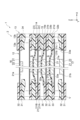
- FIG. 2 is a cross-sectional view taken along line II-II of FIG.
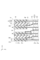
- FIG. 3 is an enlarged view of a portion of FIG.
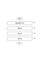
- FIG. 4 is a flowchart showing a method for manufacturing the energy storage module according to the embodiment.
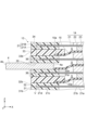
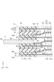
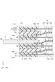
- FIG. 5 is a cross-sectional view for explaining the manufacturing method of the energy storage module according to the embodiment.
- FIG. 6 is a cross-sectional view showing an example of an end face weld portion formed by a welding process according to a comparative example.
- FIG. 7 is a cross-sectional view showing an example of an end surface welded portion formed by the welding step according to the embodiment.
- FIG. 8 is a cross-sectional view showing another example of an end surface welded portion formed by the welding step according to the embodiment.
- FIG. 1 is a schematic plan view of an electric storage module according to an embodiment.
- FIG. 2 is a cross-sectional view taken along line II-II in FIG. 1.
- FIG. 3 is a partially enlarged view of FIG. 2.
- the electric storage module 1 according to the embodiment shown in FIGS. 1 to 3 can be used as a battery for various vehicles such as a forklift, a hybrid vehicle, and an electric vehicle.
- the electric storage module 1 is, for example, a secondary battery such as a nickel-metal hydride secondary battery or a lithium-ion secondary battery.
- the electric storage module 1 may be an electric double layer capacitor or an all-solid-state battery.
- a bipolar lithium-ion secondary battery is exemplified as the electric storage module 1.
- the energy storage module 1 has a module body 2 and a pair of conductive plates (not shown).
- the module body 2 is disposed between the pair of conductive plates in the Z-axis direction.
- the pair of conductive plates apply a restraining load in the Z-axis direction to the module body 2.
- the conductive plates are conductive and also function as terminals for extracting current from the energy storage module 1.
- the conductive plates can be used to electrically connect multiple energy storage modules 1.
- a cooling flow path may be formed in the conductive plate.
- the energy storage module 1 can be cooled by circulating a cooling medium through the cooling flow path formed in the conductive plate.
- the module body 2 includes an electrode laminate (laminate) 12 and a resin sealing portion 13.
- the electrode laminate 12 is configured by stacking multiple electrodes in the Z-axis direction (first direction).
- the Z-axis direction is the stacking direction of the multiple electrodes.
- the multiple electrodes include multiple bipolar electrodes 14, a positive terminal electrode 16, and a negative terminal electrode 17. Separators 15 are interposed between adjacent electrodes.
- the multiple bipolar electrodes 14 are arranged between the positive electrode terminal electrode 16 and the negative electrode terminal electrode 17 in the Z-axis direction.
- the bipolar electrodes 14 include a current collector 21, a positive electrode active material layer 22, and a negative electrode active material layer 23.
- the current collector 21 is a chemically inactive electrical conductor that continues to pass current to the positive electrode active material layer 22 and the negative electrode active material layer 23 during discharging or charging of the lithium-ion secondary battery.
- the current collector 21 is a sheet-like conductive member having a rectangular shape in a plan view.
- the current collector 21 has a first surface 21a and a second surface 21b.
- the first surface 21a and the second surface 21b face opposite each other in the Z-axis direction.
- the current collector 21 is made of metal and is composed of, for example, a metal foil or an alloy foil.
- the metal foil include copper foil, aluminum foil, titanium foil, and nickel foil.
- Examples of the alloy foil include stainless steel foil (e.g., SUS304, SUS316, SUS301, etc., as specified in JIS G 4305:2015), plated steel foil, and stainless steel foil.
- the alloy foil may be an alloy foil of the metals exemplified as the materials for the metal foil.
- the current collector 21 may be formed by integrating or laminating a plurality of metal foils, or may be formed by plating another metal layer on the surface of one metal foil.
- the current collector 21 is formed by bonding an aluminum foil 21A and a copper foil 21B together so that the first surface 21a is an aluminum layer and the second surface 21b is a copper layer.
- the current collector 21 may be, for example, a clad foil formed by stacking and rolling-bonding an aluminum foil 21A and a copper foil 21B.
- the current collector 21 may be a laminated foil. That is, the current collector 21 may be formed by bonding and integrating an aluminum foil 21A and a copper foil 21B with a conductive adhesive resin (adhesive layer) so that the first surface 21a is an aluminum layer and the second surface 21b is a copper layer.
- the current collector 21 may be formed by copper vapor deposition or copper plating on one side of an aluminum foil so that the first surface 21a is an aluminum layer and the second surface 21b is a copper layer.
- the aluminum layer on the first surface 21a of the current collector 21 may be chromated.
- the copper layer on the second surface 21b of the current collector 21 may be nickel-plated.
- the nickel-plated layer may be a roughened surface that is a protruding plated surface with fine protrusions on the surface.
- the roughened surface may be rougher than the unprocessed metal foil, and may be formed by roughening processing such as etching or electrolytic plating.
- the thickness of the current collector 21 may be about 30 ⁇ m to 150 ⁇ m, but is not limited to this.
- the positive electrode active material layer 22 is provided on the first surface 21a of the current collector 21.
- the current collector 21 and the positive electrode active material layer 22 provided on the first surface 21a of the current collector 21 constitute the positive electrode of the bipolar electrode 14.
- the positive electrode active material layer 22 is formed in a rectangular shape in the center of the first surface 21a so that the outer edge portion 21c of the current collector 21 is exposed.
- the positive electrode active material layer 22 is provided on the first surface 21a of the current collector 21 via an adhesive layer.
- the adhesive layer may be formed of an adhesive such as acetylene black.
- the adhesive layer may be provided on the entire surface of the first surface 21a of the current collector 21.
- the edge of the adhesive layer may be formed along the edge of the negative electrode active material layer 23 that surrounds the positive electrode active material layer 22 when viewed from the Z-axis direction.
- the positive electrode active material layer 22 is a layered member including a positive electrode active material, a conductive additive, and a binder.
- the positive electrode active material include a composite oxide, metallic lithium, and sulfur.
- the composition of the composite oxide includes at least one of iron, manganese, titanium, nickel, cobalt, and aluminum, and lithium.
- the composite oxide include olivine-type lithium iron phosphate (LiFePO 4 ), LiCoO 2 , and LiNiMnCoO 2 .
- the binder serves to bind the active material or conductive assistant to the surface of the current collector 21 and maintain the conductive network in the electrode.
- binders include fluorine-containing resins such as polyvinylidene fluoride, polytetrafluoroethylene, and fluorine rubber, thermoplastic resins such as polypropylene and polyethylene, imide resins such as polyimide and polyamideimide, alkoxysilyl group-containing resins, acrylic resins containing monomer units such as acrylic acid and methacrylic acid, styrene-butadiene rubber (SBR), carboxymethyl cellulose, alginates such as sodium alginate and ammonium alginate, water-soluble cellulose ester crosslinked bodies, and starch-acrylic acid graft polymers.
- fluorine-containing resins such as polyvinylidene fluoride, polytetrafluoroethylene, and fluorine rubber
- thermoplastic resins such as polypropylene and polyethylene
- imide resins such as poly
- the positive electrode active material layer 22 may contain a viscosity adjusting solvent such as N-methyl-2-pyrrolidone (NMP).
- NMP N-methyl-2-pyrrolidone
- the negative electrode active material layer 23 is provided on the second surface 21b of the current collector 21.
- the current collector 21 and the negative electrode active material layer 23 provided on the second surface 21b of the current collector 21 constitute the negative electrode of the bipolar electrode 14.
- the negative electrode active material layer 23 is formed in a rectangular shape in the center of the second surface 21b so that the outer edge portion 21c of the current collector 21 is exposed.
- the positive electrode active material layer 22 is contained within the area of the negative electrode active material layer 23 when viewed from the Z-axis direction. That is, the outer edge of the positive electrode active material layer 22 is slightly smaller than the outer edge of the negative electrode active material layer 23.
- the negative electrode active material layer 23 is contained within the area of the conductive plate when viewed from the Z-axis direction. That is, the outer edge of the negative electrode active material layer 23 may be slightly smaller than the outer edge of the conductive plate.
- the negative electrode active material layer 23 may be provided on the second surface 21b of the current collector 21 via an adhesive layer.
- the adhesive layer used for the negative electrode active material layer 23 may be the same as the adhesive layer used for the positive electrode active material layer 22.
- the adhesive layer may be provided on the entire surface of the second surface 21b of the current collector 21.
- the negative electrode active material layer 23 is a layered member containing a negative electrode active material, a conductive additive, and a binder.
- the negative electrode active material include carbon such as graphite, artificial graphite, highly oriented graphite, mesocarbon microbeads, hard carbon, and soft carbon, metal compounds, elements that can be alloyed with lithium or compounds of such elements, and boron-added carbon. Examples of elements that can be alloyed with lithium include silicon and tin.
- the conductive additive and binder used in the negative electrode active material layer 23 may be the same as the conductive additive and binder used in the positive electrode active material layer 22.
- a conventionally known method such as roll coating, die coating, dip coating, doctor blade, spray coating, curtain coating, etc. is used.
- an active material, a solvent, and, if necessary, a binder and a conductive assistant are mixed to produce a slurry-like active material layer forming composition, which is then applied to the first surface 21a and the second surface 21b and then dried.
- the solvent include N-methyl-2-pyrrolidone, methanol, methyl isobutyl ketone, and water. The dried product may be compressed to increase the electrode density.
- the bipolar electrodes 14, 14 adjacent in the Z-axis direction are arranged so that the positive electrode active material layer 22 of one bipolar electrode 14 faces the negative electrode active material layer 23 of the other bipolar electrode 14.
- a separator 15 is arranged between the bipolar electrodes 14, 14 adjacent in the Z-axis direction.
- the separator 15 is a sheet-like member having a rectangular shape in a plan view, and prevents short circuits between the bipolar electrodes 14, 14 adjacent in the Z-axis direction.
- the separator 15 has a rectangular shape that is larger than the positive electrode active material layer 22 and the negative electrode active material layer 23 and smaller than the current collector 21 when viewed from the Z-axis direction.
- the end 15a of the separator 15 is located outside the positive electrode active material layer 22 and the negative electrode active material layer 23 when viewed from the Z-axis direction. In other words, the end 15a of the separator 15 does not overlap with either the positive electrode active material layer 22 or the negative electrode active material layer 23 when viewed from the Z-axis direction.
- the separator 15 is formed, for example, in a sheet shape.
- the separator 15 is, for example, a porous sheet or nonwoven fabric containing a polymer that absorbs and retains an electrolyte. Examples of materials constituting the separator 15 include polypropylene, polyethylene, polyolefin, and polyester.
- the separator 15 may have a single-layer structure or a multi-layer structure. In the case of a multi-layer structure, the separator 15 may include, for example, a base material layer and a pair of adhesive layers, and may be bonded and fixed to the positive electrode active material layer 22 and the negative electrode active material layer 23 by the pair of adhesive layers.
- the separator 15 may include a ceramic layer that serves as a heat-resistant layer.
- the separator 15 may be reinforced with a vinylidene fluoride resin compound.
- Separator 15 is formed by stretching molten resin using a dry process or a wet process.
- separator 15 has a direction in which it shrinks more and a direction in which it shrinks less, depending on the stretching process.
- Separator 15 may be rectangular, with the direction in which it shrinks more along the short sides and the direction in which it shrinks less along the long sides.
- One example of separator 15 is formed by a wet process, with the TD (Transverse Direction) direction in which it shrinks more along the short sides and the MD (Machine Direction) direction in which it shrinks less along the long sides.
- Examples of the electrolyte impregnated in the separator 15 include a liquid electrolyte (electrolytic solution) containing a non-aqueous solvent and an electrolyte salt dissolved in the non-aqueous solvent, or a polymer gel electrolyte containing an electrolyte held in a polymer matrix.
- a liquid electrolyte electrolytic solution
- electrolyte salt dissolved in the non-aqueous solvent
- a polymer gel electrolyte containing an electrolyte held in a polymer matrix examples of the electrolyte impregnated in the separator 15 include a liquid electrolyte (electrolytic solution) containing a non-aqueous solvent and an electrolyte salt dissolved in the non-aqueous solvent, or a polymer gel electrolyte containing an electrolyte held in a polymer matrix.
- known lithium salts such as LiClO 4 , LiAsF 6 , LiPF 6 , LiBF 4
- the positive terminal electrode 16 is composed of a current collector 21 and a positive electrode active material layer 22 provided on a first surface 21a of the current collector 21.
- the positive terminal electrode 16 is arranged on one end side in the Z-axis direction of the electrode laminate 12 so that the positive electrode active material layer 22 on the first surface 21a faces the negative electrode active material layer 23 of the terminal bipolar electrode 14.
- the positive electrode active material layer 22 and the negative electrode active material layer 23 are not provided on the second surface 21b of the current collector 21, and the second surface 21b is electrically connected to an adjacent conductive plate.
- the current collector 21 used in the positive terminal electrode 16 may be composed of aluminum foil.
- the negative terminal electrode 17 is composed of a current collector 21 and a negative active material layer 23 provided on the second surface 21b of the current collector 21.
- the negative terminal electrode 17 is arranged on the other end side in the Z-axis direction of the electrode laminate 12 so that the negative active material layer 23 on the second surface 21b faces the positive active material layer 22 of the terminal bipolar electrode 14.
- the positive active material layer 22 and the negative active material layer 23 are not provided on the first surface 21a of the current collector 21, and the first surface 21a is electrically connected to the adjacent conductive plate.
- the current collector 21 used in the negative terminal electrode 17 may be composed of copper foil.
- the separators 15 described above are arranged between the bipolar electrodes 14, 14 adjacent to each other in the Z-axis direction, as well as between the bipolar electrode 14 and the positive terminal electrode 16, and between the bipolar electrode 14 and the negative terminal electrode 17.
- the arrangement of the separators 15 prevents short circuits between the bipolar electrode 14 and the positive terminal electrode 16, and between the bipolar electrode 14 and the negative terminal electrode 17.
- the sealing portion 13 is a member that seals the internal space S between the collectors 21, 21 adjacent to each other in the Z-axis direction.
- the sealing portion 13 has electrical insulation properties.
- the sealing portion 13 is provided on the outer edge portion 21c of the collector 21 so as to surround the electrode stack 12 when viewed from the Z-axis direction.
- the sealing portion 13 is joined to the outer edge portion 21c of the collector 21.
- the sealing portion 13 is separated from the positive electrode active material layer 22 and the negative electrode active material layer 23, for example.
- the inner edge portion of the sealing portion 13 may overlap with the positive electrode active material layer 22 and the negative electrode active material layer 23.
- the sealing portion 13 When viewed from the Z-axis direction, the sealing portion 13 has a rectangular frame shape. When viewed from the Z-axis direction, the sealing portion 13 is disposed between the collectors 21, 21 adjacent to each other in the Z-axis direction so as to surround the periphery of the positive electrode active material layer 22 and the negative electrode active material layer 23. In the energy storage module 1, an internal space S is defined by the adjacent current collectors 21, 21 in the Z-axis direction and the sealing portion 13. The internal space S contains an electrolyte solution (not shown) that contains an electrolyte. The sealing portion 13 is disposed between the adjacent current collectors 21, 21 in the Z-axis direction, and therefore also functions as a spacer that maintains the distance between the adjacent current collectors 21, 21.
- the sealing portion 13 has a plurality of first sealing layers 31 made of resin, a plurality of second sealing layers 32 made of resin, and a plurality of spacer layers 33 made of resin.
- the first sealing layer 31 is spaced apart from the positive electrode active material layer 22 and joined to the outer edge portion 21c of the first surface 21a of each current collector 21.
- the second sealing layer 32 is spaced apart from the negative electrode active material layer 23 and joined to the outer edge portion 21c of the second surface 21b of each current collector 21.
- the first sealing layer 31 may be spaced apart from the negative electrode active material layer 23 or may overlap with it when viewed from the Z-axis direction.
- the first sealing layer 31 and the second sealing layer 32 are provided on the outer edge portion 21c of the current collector 21 so as to protrude from the outer edge 21d of the current collector 21.
- the first seal layer 31 and the second seal layer 32 have a frame shape (here, a rectangular frame shape) that follows the outer edge 21d of the current collector 21 when viewed from the Z-axis direction.
- the outer edge 21d constitutes the outer edge of the electrode.
- the outer edge 21d of the current collector 21 is larger than the inner edge 31a of the first seal layer 31 and the inner edge 32a of the second seal layer 32, and smaller than the outer edge 31b of the first seal layer 31 and the outer edge 32b of the second seal layer 32.
- the first seal layer 31 is bonded to the first surface 21a in the region from the inner edge 31a of the first seal layer 31 to the outer edge 21d of the current collector 21.
- the second seal layer 32 is bonded to the second surface 21b in the region from the inner edge 32a of the second seal layer 32 to the outer edge 21d of the current collector 21.
- the first sealing layer 31 and the second sealing layer 32 have, for example, the same shape as each other.
- the thickness (length in the Z-axis direction) of the first sealing layer 31 and the second sealing layer 32 may be 100 ⁇ m or more and 200 ⁇ m or less.
- the first sealing layer 31 and the second sealing layer 32 may have shapes different from each other.
- the first sealing layer 31 and the second sealing layer 32 are, for example, made of the same resin material.
- the first sealing layer 31 and the second sealing layer 32 are, for example, made of a polyolefin-based electrolyte-resistant resin material such as acid-modified polyethylene (acid-modified PE), acid-modified polypropylene (acid-modified PP), polyethylene, or polypropylene.
- the resin materials making up the first sealing layer 31 and the second sealing layer 32 may be different from each other.
- the spacer layer 33 is disposed between the first seal layer 31 and the second seal layer 32 adjacent in the Z-axis direction without the current collector 21 in between.
- the spacer layer 33 is disposed between the first seal layer 31 and the second seal layer 32 between the current collectors 21, 21 adjacent in the Z-axis direction.
- a first seal layer 31, a second seal layer 32, and a spacer layer 33 are disposed between the current collectors 21, 21 adjacent in the Z-axis direction.
- the spacer layer 33 seals the internal space S formed between the current collectors 21, 21 adjacent to each other in the Z-axis direction together with the first seal layer 31 and the second seal layer 32.
- the spacer layer 33 has a frame shape (here, a rectangular frame shape) that follows the outer edge 21d of the current collector 21.
- the outer edge 33b of the spacer layer 33 may be in the same position as the outer edge 31b of the first seal layer 31 and the outer edge 32b of the second seal layer 32.
- the spacer layer 33 is made of, for example, a resin material different from the first seal layer 31 and the second seal layer 32.
- the spacer layer 33 is made of, for example, a polyolefin-based resin material having electrolyte resistance, such as acid-modified PE, acid-modified PP, polyethylene, or polypropylene.
- the spacer layer 33 may have, for example, higher crystallinity than the first seal layer 31 and the second seal layer 32. This can suppress moisture permeation through the sealing portion 13.
- the sealing portion 13 has an inner portion 13a and an outer portion 13b.
- the inner portion 13a When viewed from the Z-axis direction, the inner portion 13a is disposed inside the outer edge 21d of the current collector 21 and is joined to the outer edge portion 21c.
- the outer portion 13b When viewed from the Z-axis direction, the outer portion 13b is disposed outside the outer edge 21d of the current collector 21.
- the inner portion 13a is configured to include inner portions of the multiple first sealing layers 31, inner portions of the multiple second sealing layers 32, and inner portions of the multiple spacer layers 33.
- the outer portion 13b is configured to include outer portions of the multiple first sealing layers 31, outer portions of the multiple second sealing layers 32, and outer portions of the multiple spacer layers 33.
- the sealing portion 13 has an end surface welding portion 34 (welded portion) at the end of the outer portion 13b separated from the inner portion 13a when viewed from the Z-axis direction, i.e., the outer edge of the sealing portion 13 is welded.
- the end surface welding portion 34 is formed by integrating the outer edges of the first sealing layers 31, the outer edges of the second sealing layers 32, and the outer edges of the spacer layers 33 with each other by welding, outside the outer edge 21d of the current collector 21 when viewed from the Z-axis direction.
- the first sealing layer 31, the second sealing layer 32, and the spacer layer 33 are not welded to each other in parts other than the end surface welding portion 34, and are only in contact with each other.
- a gap V is formed between the end surface welding portion 34 and the outer edge 21d of the current collector 21.
- the first sealing layer 31 and the second sealing layer 32 are separated from each other with the gap V in between.
- the end face welding portion 34 has a rectangular frame shape when viewed from the Z-axis direction, and surrounds the electrode stack 12.
- the side of the end face welding portion 34 opposite the internal space S extends along the Z-axis direction, and forms the outer surface of the sealing portion 13.
- the sealing portion 13 includes an inner surface facing the internal space S, and an outer surface opposite the inner surface.
- the thickness of the end face weld 34 is determined by the distance between the inner surface and the outer surface of the end face weld 34.
- the thickness of the end face weld 34 is the length of the end face weld 34 in a direction perpendicular to the outer surface.
- the thickness of the end face weld 34 is, for example, 1 mm or more and 10 mm or less. By making the thickness of the end face weld 34 1 mm or more, it is possible to suppress a decrease in sealing performance.
- the thickness of the end face weld 34 may be 3 mm or more.
- end face weld 34 If the heating time or temperature during formation of end face weld 34 is lengthened or increased in order to thicken end face weld 34, the outer surface of end face weld 34 may burn. Even if an attempt is made to provide a resin layer on such an outer surface by, for example, injection molding, it is difficult for the resin layer to weld to end face weld 34. By making the thickness of end face weld 34 10 mm or less, it is possible to prevent damage to the surface of end face weld 34.
- the sealing portion 13 has a communication hole 35 formed therein that communicates with the internal space S formed between the electrodes.
- the communication hole 35 extends in a direction intersecting the Z-axis direction. In this embodiment, the communication hole 35 extends in the X-axis direction.
- the communication hole 35 is formed by partially cutting out the spacer layer 33, and penetrates the spacer layer 33 and the end face welding portion 34.
- the communication hole 35 has one opening in the internal space S and the other opening on the outer surface of the sealing portion 13 formed by the end face welding portion 34.
- a cell including one internal space S is formed between adjacent current collectors 21, 21.
- one communication hole 35 is formed for one cell.
- the communication hole 35 can be used as a liquid injection port for injecting electrolyte into the internal space S. That is, a liquid injection port (opening of the communication hole 35) is provided on the outer surface of the sealing portion 13.
- the side on which the communication hole 35 is provided is called the liquid injection port side.
- the multiple communication holes 35 are distributed and arranged in the Y-axis direction so that the communication holes 35 provided in the internal spaces S adjacent to each other in the Z-axis direction do not overlap each other when viewed from the Z-axis direction. In FIG. 1, only one communication hole 35 is shown by a dashed line, and the other communication holes 35 are not shown.
- the inner edge 33a of the spacer layer 33 at the inlet edge is located inside (toward the internal space S) of the inner edge 31a of the first seal layer 31 and the inner edge 32a of the second seal layer 32.
- the inner edge 33a of the spacer layer 33 at the inlet edge is located, for example, 1 mm or more inside the inner edges 31a and 32a, and is exposed from the first seal layer 31 and the second seal layer 32 so as to face the internal space S.
- the inner edge 33a of the spacer layer 33 at other than the inlet edge may be located outside the inner edge 31a of the first seal layer 31 and the inner edge 32a of the second seal layer 32, or may be located inside the inner edge 31a of the first seal layer 31 and the inner edge 32a of the second seal layer 32.
- the end face welded portion 34 includes the peripheral portion 36 of the communication hole 35.
- the peripheral portion 36 faces the internal space of the communication hole 35.
- the peripheral portion 36 includes the end of the inner surface of the communication hole 35 on the outer surface side of the sealing portion 13.
- the peripheral portion 36 surrounds the communication hole 35 when viewed from the X-axis direction.
- the thickness of the peripheral portion 36 is thicker than the thickness of the portion of the end face welded portion 34 that is not the peripheral portion 36.
- the portion of the end face welded portion 34 that is not the peripheral portion 36 refers to the portion of the end face welded portion 34 other than the peripheral portion 36, or the portion of the end face welded portion 34 excluding the peripheral portion 36.
- the thickness of the end face welded portion 34 becomes thicker in the peripheral portion 36 as it approaches the communication hole 35. That is, around the liquid inlet, the thickness of the end face welded portion 34 is the thickest on the inner surface of the communication hole 35.
- the thickness of the end face welded portion 34 at the side of the liquid inlet is the length of the end face welded portion 34 in the X-axis direction.
- the thickness of the end face welded portion 34 at the side opposite the liquid inlet of the energy storage module 1 is also the length of the end face welded portion 34 in the X-axis direction.
- the thickness of the end face welded portion 34 at the two sides of the energy storage module 1 adjacent to the liquid inlet is the length of the end face welded portion 34 in the Y-axis direction.
- FIG. 4 is a flowchart showing a method for manufacturing an energy storage module according to the embodiment.
- Fig. 5 is a cross-sectional view for explaining the method for manufacturing an energy storage module according to the embodiment.
- the method for manufacturing an energy storage module 1 according to the embodiment includes a resin frame attachment step S1, a stacking step S2, a restraining step S3, and a welding step S4. By carrying out these steps in this order, the energy storage module 1 is obtained.
- the resin frame attachment process S1 is a process of providing a resin frame 11 on the electrode.
- the bipolar electrode 14 and the negative terminal electrode 17 are provided with a first seal layer 31, a second seal layer 32, and a spacer layer 33 as the resin frame 11A.
- the positive terminal electrode 16 is provided with a first seal layer 31 and a second seal layer 32 as the resin frame 11B.
- the inner parts of the first seal layer 31 and the second seal layer 32 are bonded to the outer edge parts 21c of the first surface 21a and the second surface 21b of the multiple electrodes.
- the outer parts of the first seal layer 31 and the second seal layer 32 are arranged to protrude outside the outer edge 21d of the electrode.
- the bonding of the first seal layer 31 and the second seal layer 32 may be performed using a contact type heating device such as an impulse sealer or an ultrasonic sealer, or may be performed using a non-contact type heating device such as a laser sealer.
- the spacer layer 33 is then provided on the second seal layer 32. At this time, the end 15a of the separator 15 is sandwiched between the second seal layer 32 and the spacer layer 33.
- the separator 15 and the spacer layer 33 may be partially welded to the second seal layer 32 by, for example, spot welding.
- the spacer layer 33 is provided so that the outer edge 33b coincides with the outer edge 31b of the first seal layer 31 and the outer edge 32b of the second seal layer 32.
- the resin frame portion 11 When viewed from the Z-axis direction, the resin frame portion 11 has an inner portion 11a provided inside the outer edge portion 21c of the electrode, and an outer portion 11b provided outside the outer edge portion 21c of the electrode.
- the inner portion 11a is stacked in the Z-axis direction to form the inner portion 13a of the sealing portion 13.
- the outer portion 11b is stacked in the Z-axis direction to form the outer portion 13b of the sealing portion 13.
- the lamination process S2 is a process for forming a laminate 10 by alternately laminating the electrodes with resin frames and the inserts 4 in the Z-axis direction so that the metal inserts 4 are arranged between the adjacent resin frame parts 11, 11, as shown in FIG. 5.
- the laminate 10 is a laminate that becomes the module body 2.
- the sealing part 13 is formed by laminating a plurality of resin frame parts 11 in the Z-axis direction.
- the inserts 4 are rectangular metal plates as viewed from the Z-axis direction.
- the inserts 4 are made of, for example, stainless steel.
- the inserts 4 are used to form a communication hole 35 in the sealing part 13.
- the thickness of the inserts 4 is, for example, slightly thinner than the thickness of the spacer layer 33.
- the laminate 10 is formed so that the insert 4 extends in the X-axis direction (second direction) and, as viewed from the Z-axis direction, the first end 4a of the insert 4 in the X-axis direction overlaps with the inner part of the resin frame part 11 and the second end 4b in the X-axis direction protrudes from the outer part of the resin frame part 11.
- the insert 4 is disposed in a cutout partially provided in the spacer layer 33. This cutout becomes the communication hole 35.
- a release layer such as a fluorine coating may be provided on the surface of the insert 4 to facilitate peeling from the resin.
- the release layer is provided on the part of the insert 4 near the first end 4a disposed between the resin frames 11, 11, and does not have to be provided on the part near the second end 4b protruding from the outer part of the resin frame part 11.
- the restraining step S3 is a step of restraining the laminate 10 in the Z-axis direction with a pair of restraining plates 6 so that the outer portions 11b of the laminated resin frame portions 11 protrude.
- the pair of restraining plates 6 are arranged so that, when viewed from the Z-axis direction, the end portions 11c of the outer portions of the resin frame portions 11 protrude from the restraining plates 6 together with the second ends 4b of the inserts 4.
- a resin portion 7 made of, for example, polytetrafluoroethylene (PTFE) is disposed between the restraining plates 6 and the resin frame portion 11. The restraining plates 6 are not in direct contact with the resin frame portion 11.
- PTFE polytetrafluoroethylene
- the welding process S4 is a process in which, as viewed from the Z-axis direction, the end 11c of the outer portion 11b of the resin frame portion 11 that is separated from the inner portion 11a is melted by the heater 5 to form the end surface welded portion 34. That is, in the welding process S4, the end 11c of the resin frame portion 11 that protrudes from the restraining plate 6 as viewed from the Z-axis direction is welded. As the end 11c protrudes from the restraining plate 6 in this way, it can be easily welded.
- the heater 5 has a shape extending in the Z-axis direction.
- the length of the heater 5 in the Z-axis direction is longer than the total length of the stacked resin frame parts 11 in the Z-axis direction.
- the length of the heater 5 in the Z-axis direction is, for example, 30 mm or more.
- the total length of the stacked resin frame parts 11 in the Z-axis direction is, for example, 20 mm.
- the heater 5 is, for example, a non-contact heater.
- the non-contact heater is, for example, an infrared (IR) heater.
- the non-contact heater is, for example, a carbon filament heater.
- a laser device such as an infrared laser may be used as the heater 5.
- a plurality of heaters 5 may be arranged along the sides of the rectangular laminate 10 when viewed from the Z-axis direction. That is, in the welding process S4, a plurality of heaters 5 may be arranged in a direction intersecting the Z-axis direction, specifically in the X-axis direction and the Y-axis direction.
- the heater 5 is disposed away from the insert 4 and the resin frame 11.
- the heater 5 is an IR heater
- the resin frame 11 is melted by absorbing infrared rays.
- the vibrational motion between molecules is activated by absorbing infrared rays, and the energy of the vibrational motion is converted into heat, melting the resin material.
- Metals absorb infrared rays less easily than resins. Therefore, the insert 4 is less likely to be heated by infrared rays than the resin frame 11. Also, metals have a higher heat dissipation property than resins. Therefore, the insert 4 has a higher heat dissipation property than the resin frame 11, and is more likely to lose heat.
- a portion of the input power is not converted into infrared rays, and contributes to heating the filament itself, which is the radiation source of infrared rays.
- the heated filament heats the air near the filament. Therefore, when the insert 4 is disposed near the heater 5, the insert 4 is heated by atmospheric heating in which the heat of the heater 5 is transferred through the nearby air.
- FIG. 6 is a cross-sectional view showing an example of an end face weld formed by the welding process of the comparative example. In the welding process of the comparative example, as shown in Figure 6, the end face weld 34 is not formed with sufficient thickness at the peripheral portion of the insert 4. This is because the temperature of the insert 4 is lower than that of the resin frame 11, so the heat of the resin frame 11 at the peripheral portion of the insert 4 is transferred to the insert 4 and dissipated from the insert 4.
- the insert 4 is heated by the heater 5 to a temperature equal to or higher than the melting temperature of the resin frame 11. This prevents heat from being transferred from the resin frame 11 heated by infrared rays to the insert 4. As a result, the end face welding portion 34 is formed with a thickness capable of preventing a decrease in sealing performance even in the peripheral portion 36. If the heater 5 is placed too close to the resin frame 11, the resin material may be heated not only by radiation via infrared rays, but also by heat transmitted by conduction to the air in contact with the heater 5 and by air convection, and may burn (discolor to brown).
- FIG. 7 is a cross-sectional view showing an example of an end face welded portion formed by the welding process according to the embodiment.
- FIG. 8 is a cross-sectional view showing another example of an end face welded portion formed by the welding process according to the embodiment.
- the end face welded portion 34 is formed to a sufficient thickness even in the peripheral portion 36.
- the insert 4 may be heated so that the thickness of the end face welded portion 34 is thicker in the peripheral portion 36 than in other portions.
- the insert 4 may be heated so that the thickness of the end face welded portion 34 is equal to or greater than in other portions in the peripheral portion 36.
- the insert 4 is removed after the welding process S4, and electrolyte is injected into the internal space S from the communication hole 35.
- the restraining plate 6 and the resin portion 7 are removed from the energy storage module 1 after the electrolyte is injected.
- the insert 4 is heated by the heater 5 to a temperature equal to or higher than the melting temperature of the resin frame portion 11, so heat is unlikely to transfer from the peripheral portion of the insert 4 to the insert 4.
- the end face welded portion 34 is formed with a sufficient thickness even in the peripheral portion of the insert 4, i.e., the peripheral portion 36 of the communication hole 35. As a result, deterioration of sealing performance can be suppressed.
- the insert 4 is heated by the heat of the heater 5, which is a non-contact heater. Therefore, the insert 4 can be heated by the heater 5 to a temperature equal to or higher than the melting temperature of the resin frame portion 11.
- the insert 4 may be heated so that the thickness of the peripheral portion 36 of the end face welded portion 34 becomes equal to or greater than the thickness of the portion of the end face welded portion 34 that is not the peripheral portion 36. In this case, it is possible to reliably prevent a decrease in sealing performance.
- the insert 4 may be heated so that the thickness of the peripheral portion 36 of the end face welded portion 34 becomes thicker than the thickness of the portion of the end face welded portion 34 that is not the peripheral portion 36. In this case, it is possible to more reliably prevent a decrease in sealing performance.
- the thickness of the end face welded portion 34 may increase in the peripheral portion 36 as it approaches the communication hole 35. In this case, the thickness of the end face welded portion 34 is the thickest on the inner surface of the communication hole 35. Therefore, it is possible to more reliably prevent a decrease in sealing performance.
- the heater 5 has a shape that extends in the Z-axis direction.
- the heater 5 is longer than the laminate 10 in the Z-axis direction.
- multiple heaters 5 are arranged in a direction that intersects with the Z-axis direction. This allows the end face welded portion 34 to be formed efficiently.
- the resin frame portion 11A provided on the bipolar electrode 14 has a first seal layer 31 bonded to the outer edge portion 21c of the first surface 21a of the bipolar electrode 14, a second seal layer 32 bonded to the outer edge portion 21c of the second surface 21b of the bipolar electrode 14, and a spacer layer 33 disposed on the first seal layer 31.
- the first seal layer 31 and the second seal layer 32 can improve the bond of the resin frame portion 11A to the bipolar electrode 14.
- the spacer layer 33 can reliably separate adjacent electrodes.
- the end face welded portion 34 is formed with sufficient thickness even in the peripheral portion 36 of the communication hole 35. As a result, deterioration of the sealing performance can be suppressed.
- the insert 4 may be heated by the heater 5 to a temperature equal to or higher than the melting temperature of the resin frame 11, and may be heated such that the thickness of the end face welded portion 34 is thinner at the peripheral portion 36 than at other portions. Even in this case, the thickness of the end face welded portion 34 at the peripheral portion 36 is thicker than in a configuration in which the insert 4 is not heated by the heater 5 to a temperature equal to or higher than the melting temperature of the resin frame 11. This makes it possible to suppress a decrease in sealing performance.
- a spacer layer 33 is provided on the second seal layer 32 of the bipolar electrode 14 and the negative terminal electrode 17, but a spacer layer 33 may also be provided on the first seal layer 31 of the bipolar electrode 14 and the positive terminal electrode 16.
- a method for manufacturing an electricity storage module comprising: a stack in which a plurality of electrodes including a bipolar electrode are stacked in a first direction; and a sealing portion in which a plurality of resin frame portions are stacked in the first direction and provided on outer edges of the electrodes so as to surround the stack when viewed from the first direction, each of the plurality of resin frame portions having an outer portion provided on the outer side of the electrode and an inner portion provided on the inner side of the electrode when viewed from the first direction, a resin frame attachment step of joining the inner portion to an outer edge of the electrode to form a resin-framed electrode; a lamination step of alternately laminating the resin-framed electrodes and the metal inserts in the first direction so that the metal inserts are disposed between the resin frame parts adjacent to each other in the first direction to form a laminate; a restraining step of restraining the laminate in the first direction by a pair of restraint plates; a welding step
- a method for manufacturing an energy storage module [Clause 2] the heater is a non-contact heater, In the welding step, the insert is heated by the heat of the non-contact heater. 2. A method for manufacturing the storage module according to claim 1. [Clause 3] In the restraining step, the end portion of the outer portion is provided on the outer side of the restraining plate as viewed from the first direction. 3. A method for manufacturing the storage module according to claim 1 or 2. [Clause 4] In the welding step, the insert is heated so that a thickness of a peripheral portion of the insert at the welding portion is equal to or greater than a thickness of a portion other than the peripheral portion of the welding portion. A method for manufacturing the storage module according to any one of claims 1 to 3.
- the heater has a shape extending in the first direction, the heater is longer than the stack in the first direction; In the welding step, a plurality of the heaters are arranged in a direction intersecting the first direction.
- Item 5 A method for manufacturing the storage module according to any one of items 1 to 4.
- the resin frame portion provided on the bipolar electrode includes a first seal layer joined to the outer edge portion of a first surface of the bipolar electrode, a second seal layer joined to the outer edge portion of a second surface of the bipolar electrode opposite to the first surface, and a spacer layer disposed on the first seal layer or the second seal layer. 6.
- Energy storage module. [Clause 8] The thickness of the welded portion is increased toward the communication hole in the peripheral portion. 8. The energy storage module of claim 7.
- 1... Electricity storage module 4... Nest, 4a... First end, 4b... Second end, 5... Heater, 6... Restriction plate, 10... Laminated body, 11, 11A, 11B... Resin frame, 11 a...Inner part, 11b...Outer part, 11c...End part, 12...Electrode laminate (laminate), 13...Sealing part, 13a...Inner part, 13b...Outer part, 14...Bipo 21a...first surface, 21b...second surface, 21c...outer edge, 21d...outer edge, 31...first seal layer, 32...second seal layer, 33...spacer layer, 34...
- End face welding part welding part
- 35...Communication hole 36...Peripheral part
- S...Internal space S1...Resin frame attachment process
- S2...Lamination process S3...Restraint process
- S4...Welding process S1...Resin frame attachment process
Landscapes
- Engineering & Computer Science (AREA)
- Chemical & Material Sciences (AREA)
- Chemical Kinetics & Catalysis (AREA)
- Electrochemistry (AREA)
- General Chemical & Material Sciences (AREA)
- Power Engineering (AREA)
- Manufacturing & Machinery (AREA)
- Microelectronics & Electronic Packaging (AREA)
- Sealing Battery Cases Or Jackets (AREA)
Priority Applications (2)
| Application Number | Priority Date | Filing Date | Title |
|---|---|---|---|
| CN202480074912.5A CN122295778A (zh) | 2023-11-27 | 2024-11-21 | 蓄电模块的制造方法和蓄电模块 |
| JP2025561063A JPWO2025115754A1 (cg-RX-API-DMAC7.html) | 2023-11-27 | 2024-11-21 |
Applications Claiming Priority (2)
| Application Number | Priority Date | Filing Date | Title |
|---|---|---|---|
| JP2023-199950 | 2023-11-27 | ||
| JP2023199950 | 2023-11-27 |
Publications (1)
| Publication Number | Publication Date |
|---|---|
| WO2025115754A1 true WO2025115754A1 (ja) | 2025-06-05 |
Family
ID=95896602
Family Applications (1)
| Application Number | Title | Priority Date | Filing Date |
|---|---|---|---|
| PCT/JP2024/041311 Pending WO2025115754A1 (ja) | 2023-11-27 | 2024-11-21 | 蓄電モジュールの製造方法及び蓄電モジュール |
Country Status (3)
| Country | Link |
|---|---|
| JP (1) | JPWO2025115754A1 (cg-RX-API-DMAC7.html) |
| CN (1) | CN122295778A (cg-RX-API-DMAC7.html) |
| WO (1) | WO2025115754A1 (cg-RX-API-DMAC7.html) |
Citations (2)
| Publication number | Priority date | Publication date | Assignee | Title |
|---|---|---|---|---|
| JP2018174079A (ja) * | 2017-03-31 | 2018-11-08 | 株式会社豊田自動織機 | 蓄電モジュールおよびその製造方法 |
| JP2023147142A (ja) * | 2022-03-29 | 2023-10-12 | 株式会社豊田自動織機 | 蓄電装置 |
-
2024
- 2024-11-21 JP JP2025561063A patent/JPWO2025115754A1/ja active Pending
- 2024-11-21 WO PCT/JP2024/041311 patent/WO2025115754A1/ja active Pending
- 2024-11-21 CN CN202480074912.5A patent/CN122295778A/zh active Pending
Patent Citations (2)
| Publication number | Priority date | Publication date | Assignee | Title |
|---|---|---|---|---|
| JP2018174079A (ja) * | 2017-03-31 | 2018-11-08 | 株式会社豊田自動織機 | 蓄電モジュールおよびその製造方法 |
| JP2023147142A (ja) * | 2022-03-29 | 2023-10-12 | 株式会社豊田自動織機 | 蓄電装置 |
Also Published As
| Publication number | Publication date |
|---|---|
| CN122295778A (zh) | 2026-06-26 |
| JPWO2025115754A1 (cg-RX-API-DMAC7.html) | 2025-06-05 |
Similar Documents
| Publication | Publication Date | Title |
|---|---|---|
| JP2023087348A (ja) | 蓄電装置の製造方法及び蓄電装置 | |
| JP2021082450A (ja) | 蓄電モジュールの製造方法 | |
| WO2022264583A1 (ja) | 蓄電装置の製造方法 | |
| JP2023110291A (ja) | 蓄電モジュール | |
| JP2024162813A (ja) | 蓄電モジュール | |
| JP7779204B2 (ja) | 蓄電装置 | |
| KR102834032B1 (ko) | 축전 셀 및 축전 장치 | |
| JP7757859B2 (ja) | 蓄電装置 | |
| CN119072810A (zh) | 电极的制造方法 | |
| KR20240119320A (ko) | 축전 장치 | |
| JP7750402B2 (ja) | 蓄電装置 | |
| US20250201984A1 (en) | Power storage device | |
| KR102841786B1 (ko) | 축전 장치 | |
| US20260074334A1 (en) | Electric power storage module | |
| JP2021103663A (ja) | 蓄電モジュールの製造方法及び蓄電モジュール | |
| WO2024053312A1 (ja) | 蓄電装置 | |
| JP7852478B2 (ja) | 蓄電装置 | |
| JP7740533B2 (ja) | 蓄電モジュール | |
| EP4513603A1 (en) | Electrode manufacturing method | |
| US20250219206A1 (en) | Power storage module and manufacturing method of power storage module | |
| WO2025047414A1 (ja) | 蓄電モジュール | |
| JP2025051097A (ja) | 蓄電装置の製造方法 | |
| JP2025097647A (ja) | 蓄電モジュールの製造方法及び蓄電モジュールの製造装置 | |
| JP2025082960A (ja) | 電池の製造方法、及び、電池 | |
| JP2024162815A (ja) | 蓄電モジュール |
Legal Events
| Date | Code | Title | Description |
|---|---|---|---|
| 121 | Ep: the epo has been informed by wipo that ep was designated in this application |
Ref document number: 24897440 Country of ref document: EP Kind code of ref document: A1 |
|
| ENP | Entry into the national phase |
Ref document number: 2025561063 Country of ref document: JP Kind code of ref document: A |
|
| WWE | Wipo information: entry into national phase |
Ref document number: 2025561063 Country of ref document: JP |
|
| NENP | Non-entry into the national phase |
Ref country code: DE |