WO2025115602A1 - 基板処理方法および基板処理システム - Google Patents
基板処理方法および基板処理システム Download PDFInfo
- Publication number
- WO2025115602A1 WO2025115602A1 PCT/JP2024/040233 JP2024040233W WO2025115602A1 WO 2025115602 A1 WO2025115602 A1 WO 2025115602A1 JP 2024040233 W JP2024040233 W JP 2024040233W WO 2025115602 A1 WO2025115602 A1 WO 2025115602A1
- Authority
- WO
- WIPO (PCT)
- Prior art keywords
- glass substrate
- silicon
- containing film
- film
- substrate
- Prior art date
- Legal status (The legal status is an assumption and is not a legal conclusion. Google has not performed a legal analysis and makes no representation as to the accuracy of the status listed.)
- Pending
Links
Images





Classifications
-
- C—CHEMISTRY; METALLURGY
- C03—GLASS; MINERAL OR SLAG WOOL
- C03C—CHEMICAL COMPOSITION OF GLASSES, GLAZES OR VITREOUS ENAMELS; SURFACE TREATMENT OF GLASS; SURFACE TREATMENT OF FIBRES OR FILAMENTS MADE FROM GLASS, MINERALS OR SLAGS; JOINING GLASS TO GLASS OR OTHER MATERIALS
- C03C17/00—Surface treatment of glass, not in the form of fibres or filaments, by coating
- C03C17/22—Surface treatment of glass, not in the form of fibres or filaments, by coating with other inorganic material
-
- C—CHEMISTRY; METALLURGY
- C23—COATING METALLIC MATERIAL; COATING MATERIAL WITH METALLIC MATERIAL; CHEMICAL SURFACE TREATMENT; DIFFUSION TREATMENT OF METALLIC MATERIAL; COATING BY VACUUM EVAPORATION, BY SPUTTERING, BY ION IMPLANTATION OR BY CHEMICAL VAPOUR DEPOSITION, IN GENERAL; INHIBITING CORROSION OF METALLIC MATERIAL OR INCRUSTATION IN GENERAL
- C23C—COATING METALLIC MATERIAL; COATING MATERIAL WITH METALLIC MATERIAL; SURFACE TREATMENT OF METALLIC MATERIAL BY DIFFUSION INTO THE SURFACE, BY CHEMICAL CONVERSION OR SUBSTITUTION; COATING BY VACUUM EVAPORATION, BY SPUTTERING, BY ION IMPLANTATION OR BY CHEMICAL VAPOUR DEPOSITION, IN GENERAL
- C23C16/00—Chemical coating by decomposition of gaseous compounds, without leaving reaction products of surface material in the coating, i.e. chemical vapour deposition [CVD] processes
- C23C16/22—Chemical coating by decomposition of gaseous compounds, without leaving reaction products of surface material in the coating, i.e. chemical vapour deposition [CVD] processes characterised by the deposition of inorganic material, other than metallic material
- C23C16/24—Deposition of silicon only
-
- C—CHEMISTRY; METALLURGY
- C23—COATING METALLIC MATERIAL; COATING MATERIAL WITH METALLIC MATERIAL; CHEMICAL SURFACE TREATMENT; DIFFUSION TREATMENT OF METALLIC MATERIAL; COATING BY VACUUM EVAPORATION, BY SPUTTERING, BY ION IMPLANTATION OR BY CHEMICAL VAPOUR DEPOSITION, IN GENERAL; INHIBITING CORROSION OF METALLIC MATERIAL OR INCRUSTATION IN GENERAL
- C23C—COATING METALLIC MATERIAL; COATING MATERIAL WITH METALLIC MATERIAL; SURFACE TREATMENT OF METALLIC MATERIAL BY DIFFUSION INTO THE SURFACE, BY CHEMICAL CONVERSION OR SUBSTITUTION; COATING BY VACUUM EVAPORATION, BY SPUTTERING, BY ION IMPLANTATION OR BY CHEMICAL VAPOUR DEPOSITION, IN GENERAL
- C23C16/00—Chemical coating by decomposition of gaseous compounds, without leaving reaction products of surface material in the coating, i.e. chemical vapour deposition [CVD] processes
- C23C16/56—After-treatment
-
- H—ELECTRICITY
- H10—SEMICONDUCTOR DEVICES; ELECTRIC SOLID-STATE DEVICES NOT OTHERWISE PROVIDED FOR
- H10P—GENERIC PROCESSES OR APPARATUS FOR THE MANUFACTURE OR TREATMENT OF DEVICES COVERED BY CLASS H10
- H10P72/00—Handling or holding of wafers, substrates or devices during manufacture or treatment thereof
- H10P72/30—Handling or holding of wafers, substrates or devices during manufacture or treatment thereof for conveying, e.g. between different workstations
Definitions
- Various aspects and embodiments of the present disclosure relate to substrate processing methods and substrate processing systems.
- Patent Document 1 discloses that "When multiple cut thin glass substrates are combined and used as a light guide plate, the cut thin glass substrates are typically stacked and used as the light guide plate. The light guide is applied to display devices such as head-mounted displays.”
- the present disclosure provides a substrate processing method and a substrate processing system that can perform processes such as film formation and etching on glass substrates.
- the processing target is a glass substrate, and to perform processing such as film formation and etching on the glass substrate.
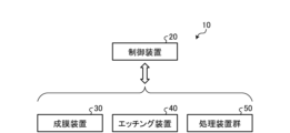
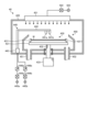
- FIG. 1 is a system configuration diagram illustrating an example of a substrate processing system according to an embodiment of the present disclosure.
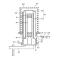
- FIG. 2 is a schematic cross-sectional view showing an example of the configuration of a film forming apparatus.
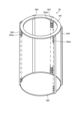
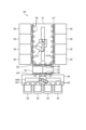
- FIG. 3 is a diagram showing an example of a structure of a boat.
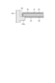
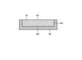
- FIG. 4 is an enlarged cross-sectional view showing an example of the vicinity of a claw portion of a boat.
- FIG. 5 is a schematic cross-sectional view showing an example of an etching apparatus.
- FIG. 6 is a plan view showing an example of a processing apparatus group.
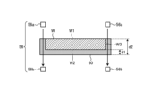
- FIG. 7 is a diagram for explaining an example of a sensing method.
- FIG. 8 is a flowchart showing an example of a substrate processing method according to the first embodiment.
- FIG. 8 is a flowchart showing an example of a substrate processing method according to the first embodiment.
- FIG. 9A is a diagram showing an example of a process for processing a glass substrate.
- FIG. 9B is a diagram showing an example of a process of processing a glass substrate.
- FIG. 9C is a diagram showing an example of a process for processing a glass substrate.
- FIG. 10 is a diagram showing an example of transmittance for each combination of film thickness and light wavelength when the protective film is made of polysilicon.
- FIG. 11 is a diagram showing an example of transmittance for each combination of film thickness and light wavelength when the protective film is made of amorphous silicon.
- FIG. 12 is a flowchart showing an example of a substrate processing method according to the second embodiment.
- FIG. 13A is a diagram showing an example of a process for processing a glass substrate.
- FIG. 13A is a diagram showing an example of a process for processing a glass substrate.
- FIG. 13B is a diagram showing an example of a process for treating a glass substrate.
- FIG. 13C is a diagram showing an example of a process for processing a glass substrate.
- FIG. 13D is a diagram showing an example of a process for treating a glass substrate.
- FIG. 13E is a diagram showing an example of a process for treating a glass substrate.
- FIG. 13F is a diagram showing an example of a process for processing a glass substrate.
- microfabrication technology using glass substrates has been used to manufacture high-performance optical elements such as AR (Augmented Reality) glass.
- processes such as etching and film deposition are performed on glass substrates.
- commercially available glass substrates may have metal elements used during the manufacturing process attached to their surfaces. Therefore, when commercially available glass substrates are used as is in a processing device for etching, film formation, or other processes, the components inside the processing device that come into contact with the glass substrate may become contaminated with metal elements. If the components inside the processing device are contaminated with metal elements, the metal elements may become mixed in during the etching or film formation process on the glass substrate, causing defects in the optical element.
- This disclosure has an aspect that can suppress metal contamination inside processing equipment caused by glass substrates.
- FIG. 10 is a system configuration diagram showing an example of a substrate processing system 10 according to an embodiment of the present disclosure.
- the substrate processing system 10 according to the present embodiment includes a control device 20, a film forming device 30, an etching device 40, and a processing device group 50.
- the film forming device 30 forms a protective film on both surfaces and the side of the glass substrate W, thereby covering both surfaces and the side of the glass substrate W with the protective film.
- the protective film is a silicon-containing film such as polysilicon or amorphous silicon.
- the etching device 40 removes the protective film that covers the surface (hereinafter referred to as the first surface) of the glass substrate W that is covered with the protective film and on which processing such as film formation and etching is performed.
- the etching device 40 is an example of a removal device.
- the processing device group 50 includes processing devices that perform processes such as film formation and etching on the glass substrate W.
- the processing devices perform processes such as film formation and etching on the first surface of the glass substrate W from which the protective film has been removed.
- the control device 20 has a memory, a processor, and an input/output interface. Data such as recipes and programs are stored in the memory.
- the memory is, for example, a RAM (Random Access Memory), a ROM (Read Only Memory), a HDD (Hard Disk Drive), or an SSD (Solid State Drive).
- the processor is, for example, a CPU (Central Processing Unit) or a DSP (Digital Signal Processor). The processor executes a program read from the memory, and controls each part of the film forming device 30, the etching device 40, and the processing device group 50 via the input/output interface based on data such as recipes stored in the memory.
- Fig. 2 is a schematic cross-sectional view showing an example of the configuration of the film formation apparatus 30.
- Fig. 2 shows a batch-type vertical heat treatment apparatus as an example of the film formation apparatus 30.
- the film formation apparatus 30 may be a single-wafer type film formation apparatus as long as it is an apparatus capable of forming a silicon-containing film on both surfaces and a side surface of a glass substrate.
- the film forming apparatus 30 is equipped with a substantially cylindrical reaction tube 32 whose longitudinal direction extends vertically.
- the reaction tube 32 has a double-tube structure including an inner tube 33 and an outer tube 34 with a ceiling that covers the inner tube 33 and is formed to have a certain distance from the inner tube 33.
- the inner tube 33 and the outer tube 34 are formed from a material with excellent heat resistance and corrosion resistance, such as quartz.
- the manifold 35 is airtightly connected to the lower end of the outer tube 34.
- the inner tube 33 protrudes from the inner wall of the manifold 35 and is supported by a support ring 36 formed integrally with the manifold 35.
- a lid body 37 is disposed below the manifold 35.
- the lid body 37 is configured to be movable up and down by a boat elevator 38.
- the lid body 37 is raised by the boat elevator 38, the lower side (furnace opening portion) of the manifold 35 is closed.
- the lid body 37 is lowered by the boat elevator 38, the lower side (furnace opening portion) of the manifold 35 is opened.
- a boat 39 made of, for example, quartz is placed on the lid 37.
- the boat 39 is configured to accommodate multiple glass substrates W at predetermined intervals along the extension direction of the reaction tube 32.
- Figure 3 shows an example of the structure of the boat 39.
- the boat 39 has a top plate 391 and a bottom plate 392.
- a plurality of pillars 393 are provided between the top plate 391 and the bottom plate 392.
- Auxiliary pillars 394 are provided between the pillars 393.
- the pillars 393 are provided with claw portions 393a at predetermined intervals for supporting the glass substrates W.
- the claw portions 393a protrude toward the center of the boat 39 and are formed to have a surface that is approximately parallel to the top plate 391 and the bottom plate 392.
- Figure 4 is an enlarged cross-sectional view showing an example of the vicinity of the claw portion 393a of the boat 39.
- the claw portion 393a supports the edge portion of the glass substrate W on the upper surface of the claw portion 393a. This allows a protective film 60 to be formed on the first surface W1 of the glass substrate W, the second surface W2 behind the first surface W1, and the side surface W3 of the glass substrate W.
- the first surface W1 of the glass substrate W is the surface on which the optical elements are formed.
- an insulator 311 is provided so as to surround the reaction tube 32.
- a heater 312, such as a resistance heating element, is provided on the inner wall surface of the insulator 311. The heater 312 heats the inside of the reaction tube 32 to a predetermined temperature, and the glass substrate W is heated to the predetermined temperature.
- Pipes 313 for introducing multiple process gases are connected to the side of the manifold 35. Specifically, the pipes 313 are connected to the side of the manifold 35 below the support ring 36 (below the inner tube 33). The pipes 313 supply process gas to the space within the reaction tube 32. Note that, although one pipe 313 is depicted in the example of FIG. 2, a number of pipes 313 may be connected according to the type of process gas supplied to the space within the inner tube 33. In this embodiment, in order to form a protective film 60, which is a silicon-containing film, on the surface of the glass substrate W, for example, silane gas is used as the process gas.
- the pipe 313 is connected to a process gas supply source (not shown) via a mass flow controller (not shown) or the like. This allows a predetermined amount of process gas to be supplied from the process gas supply source via the pipe 313 to the space within the reaction tube 32.
- the side of the manifold 35 is provided with an exhaust port 314 for exhausting gas from the space inside the reaction tube 32.
- the exhaust port 314 is provided above the support ring 36 and communicates with the space formed between the inner tube 33 and the outer tube 34 inside the reaction tube 32.
- An exhaust pipe 316 is airtightly connected to the exhaust port 314.
- a valve 17 and a vacuum pump 318 are provided on the exhaust pipe 316.
- the valve 317 adjusts the opening of the exhaust pipe 316 to control the pressure inside the reaction tube 32 to a predetermined pressure.
- the vacuum pump 318 exhausts the gas inside the reaction tube 32 via the exhaust pipe 316.
- a pipe 315 for supplying purge gas is inserted below the exhaust port 314 on the side of the manifold 35.
- a purge gas supply source (not shown) is connected to the pipe 315, and a predetermined amount of purge gas (e.g., nitrogen gas) is supplied from the purge gas supply source through the pipe 315 into the reaction tube 32.
- purge gas e.g., nitrogen gas
- FIG. 5 is a schematic cross-sectional view showing an example of the etching apparatus 40.
- the etching apparatus 40 includes a chamber 420, a substrate holding mechanism 430, a liquid supply unit 440, and a collection cup 450.
- the chamber 420 houses a substrate holding mechanism 430, a liquid supply unit 440, and a collection cup 450.
- An FFU (Fan Filter Unit) 421 is provided on the ceiling of the chamber 420. The FFU 421 creates a downflow within the chamber 420.
- the FFU 421 is connected to a gas supply source 423 via a valve 422.
- the FFU 421 discharges gas such as dry air supplied from the gas supply source 423 into the chamber 420.
- the substrate holding mechanism 430 includes a rotating holding part 431, a support part 432, and a driving part 433.
- the rotating holding part 431 is provided in approximately the center of the chamber 420.
- a holding member 4311 that holds the glass substrate W from the side is provided on the upper surface of the rotating holding part 431.
- the holding member 4311 holds the glass substrate W so that the first surface W1 faces upward.
- the holding member 4311 also holds the glass substrate W horizontally with the glass substrate W slightly spaced from the upper surface of the rotating holding part 431.
- the support portion 432 is a member extending in the vertical direction, its base end is rotatably supported by the drive portion 433, and its tip end horizontally supports the rotation holder 431.
- the drive portion 433 rotates the support portion 432 around the vertical axis.
- the substrate holding mechanism 430 rotates the support part 432 using the drive part 433, thereby rotating the rotating holding part 431 supported by the support part 432. This causes the glass substrate W held by the rotating holding part 431 to rotate.
- the rotating holder 431 is not limited to a type that holds the glass substrate W from the side, but may be a type that holds the glass substrate W by suction from below, such as a vacuum chuck.
- the liquid supply unit 440 supplies various processing liquids to the glass substrate W held by the substrate holding mechanism 430.
- the liquid supply unit 440 includes multiple nozzles 441a, 441b (two in the example of FIG. 5), an arm 442 that horizontally supports the nozzles 441a, 441b, and a pivoting and lifting mechanism 443 that pivots and raises and lowers the arm 442. Note that the nozzles 441a and 441b may be supported by separate arms.
- An etching liquid supply source 445a is connected to the nozzle 441a via a valve 444a and a flow regulator 446a.
- a rinsing liquid supply source 445b is connected to the nozzle 441b via a valve 444b and a flow regulator 446b.
- the etching solution supplied from the etching solution supply source 445a is discharged from the nozzle 441a.
- the etching solution in this embodiment is, for example, TMAH (tetramethylammonium hydroxide), fluoronitric acid, or fluoronitric acid acetic acid.
- Rinse liquid supplied from rinse liquid supply source 445b is ejected from nozzle 441b.
- the rinse liquid is, for example, DIW (deionized water).
- the collection cup 450 is disposed to surround the rotating holder 431, and collects the processing liquid scattered from the glass substrate W by the rotation of the rotating holder 431.
- a drain port 451 is formed at the bottom of the collection cup 450, and the processing liquid collected by the collection cup 450 is discharged from the drain port 451 to the outside of the etching apparatus 40.
- an exhaust port 452 is formed at the bottom of the collection cup 450, which discharges the gas supplied from the FFU 421 to the outside of the etching apparatus 40.
- the number of nozzles provided in the etching device 40 is not limited to the above example, and may be, for example, a configuration including a single nozzle that ejects the etching liquid and the rinsing liquid.
- An etching solution is supplied from the nozzle 441a to the glass substrate W held by the holding member 4311 with the first surface W1 facing upward, thereby removing the protective film 60 formed on the first surface W1 of the glass substrate W. At this time, the protective film 60 formed on the second surface W2 and side surface W3 of the glass substrate W remains without being removed.
- FIG. 6 is a plan view showing an example of a processing apparatus group 50.
- the processing apparatus group 50 includes a vacuum transfer chamber 51, a plurality of processing apparatuses 52, a plurality of load lock chambers 53, and an atmospheric transfer chamber 54.
- the vacuum transfer chamber 51 is an example of a transfer chamber.
- a processing device 52 is connected to the side wall of the vacuum transfer chamber 51 via a gate valve G1. Note that, in the example of FIG. 6, eight processing devices 52 are connected to the vacuum transfer chamber 51, but the disclosed technology is not limited to this. The number of processing devices 52 connected to the vacuum transfer chamber 51 may be seven or less, or nine or more.
- each processing device 52 processes the first surface W1 of the glass substrate W by performing processes such as film formation and etching on the first surface W1 of the glass substrate W, thereby processing the first surface W1 of the glass substrate W or forming a structure on the first surface W1 of the glass substrate W.
- a number of load lock chambers 53 are connected to the other side wall of the vacuum transfer chamber 51 via gate valve G2.
- two load lock chambers 53 are connected to the vacuum transfer chamber 51, but the disclosed technology is not limited to this.
- the number of load lock chambers 53 connected to the vacuum transfer chamber 51 may be one, or three or more.
- a transfer device 511 is disposed within the vacuum transfer chamber 51.
- the transfer device 511 moves within the vacuum transfer chamber 51 along a guide rail 510 provided within the vacuum transfer chamber 51.
- the transfer device 511 transfers the glass substrate W between the processing device 52 and the load lock chamber 53.
- the interior of the vacuum transfer chamber 51 is maintained at a pressure atmosphere lower than atmospheric pressure. Note that the transfer device 511 may be configured to be fixed at a predetermined position within the vacuum transfer chamber 51 and not to move within the vacuum transfer chamber 51.
- One side wall of the load lock chamber 53 is connected to the vacuum transfer chamber 51 via gate valve G2, and the other side wall is connected to the atmospheric transfer chamber 54 via gate valve G3.
- a plurality of load ports 55 are provided on a side wall of the atmospheric transfer chamber 54 other than the side wall on which the gate valve G3 is provided.
- Each load port 55 is connected to a container such as a FOUP (Front Opening Unified Pod) capable of accommodating a plurality of glass substrates W.
- the atmospheric transfer chamber 54 may be provided with an aligner module or the like that changes the orientation of the glass substrates W.
- the pressure inside the atmospheric transfer chamber 54 is atmospheric pressure.
- a transfer device 541 is provided inside the atmospheric transfer chamber 54.
- the transfer device 541 moves inside the atmospheric transfer chamber 54 along a guide rail 540 provided inside the atmospheric transfer chamber 54, and transfers the glass substrate W between the load lock chamber 53 and a container connected to the load port 55.
- the transfer device 541 may be fixed at a predetermined position inside the atmospheric transfer chamber 54 and may not move inside the atmospheric transfer chamber 54.
- the protective film 60 is formed too thick on the glass substrate W. However, if the protective film 60 is too thin, the light emitted from the light emitting portion 56a will pass through the protective film 60.
- the protective film 60 is also formed on the side surface W3 of the glass substrate W.
- the light emitting portion 56a emits light in a direction along the side surface W3 (thickness direction of the glass substrate W) to the protective film 60 formed on the side surface W3 of the glass substrate W. Since the glass substrate W has a thickness of 700 ⁇ m or more, the protective film 60 formed on the side surface W3 has a thickness of 700 ⁇ m or more in the direction along the side surface W3. As a result, even if the protective film 60 is not formed so thick on the second surface W2 of the glass substrate W, the protective film 60 formed on the side surface W3 can block the light emitted from the light emitting portion 56a. As a result, in this embodiment, the position of the glass substrate W can be detected by the sensor 56 while preventing deformation of the glass substrate W.
- commercially available glass substrates W may have metal elements, etc., used during the manufacturing process, adhering to their surfaces. Therefore, if a commercially available glass substrate W is used as is in processing equipment 52 for etching, film formation, etc., the members inside the chamber of processing equipment 52 that come into contact with the glass substrate W may be contaminated with metal elements. If the members inside the chamber are contaminated with metal elements, the metal elements may get mixed in during the etching or film formation process on the glass substrate W, causing defects in the optical element.
- step S10 the glass substrate W is covered with a protective film 60 having a thickness of 40 nm or more. This makes it possible to prevent the components in the chamber of the processing device 52 that come into contact with the glass substrate W from being contaminated with metal elements during the subsequent etching and film formation processes on the glass substrate W.
- step S11 is an example of process b).
- step S11 as shown in FIG. 9B, for example, the protective film 60 formed on the first surface W1 of the glass substrate W is removed by the etching device 40, and the first surface W1 is exposed.
- step S11 the second surface W2 and the side surface W3 remain covered with the protective film 60.
- the protective film 60 formed on at least one of the second surface W2 and the side surface W3 can block the light emitted from the light emitting element 56a, making it possible to detect the position of the glass substrate W.
- the substrate processing method in the first embodiment includes steps a) and b).
- a silicon-containing film (protective film 60) is formed on a first surface (first surface W1) of a glass substrate (glass substrate W) and a second surface (second surface W2) that is the reverse surface of the first surface.
- the silicon-containing film formed on the first surface is removed. This makes it possible to suppress metal contamination by the glass substrate.
- the first embodiment described above is a substrate processing system 10 that includes a film forming apparatus (film forming apparatus 30), a removal apparatus (etching apparatus 40), and a processing apparatus (processing apparatus 52).
- the film forming apparatus forms a silicon-containing film on a first surface of a glass substrate and a second surface that is the reverse side of the first surface, and the removal apparatus removes the silicon-containing film formed on the first surface of the glass substrate.
- the processing apparatus performs at least one of film forming and etching processes on the first surface of the glass substrate from which the silicon-containing film has been removed. This makes it possible to suppress metal contamination by the glass substrate.
- the protective film 60 on the first surface W1 on which the optical elements are to be formed is removed, and the optical elements are formed on the first surface W1 from which the protective film 60 has been removed.
- the protective film 60 formed on the first surface W1 on which the optical elements are to be formed is processed to form optical elements that include a part of the protective film 60 formed on the first surface W1. The following will mainly describe the parts that are different from the first embodiment.
- FIG. 12 is a flowchart showing an example of a substrate processing method according to the second embodiment. The process shown in Fig. 12 is realized by the control device 20 controlling each part of the film forming device 30, the etching device 40, and the processing device group 50.
- a protective film 60 is formed on the glass substrate W (step S20).
- Step S20 is an example of process c).
- the protective film 60 which is a silicon-containing film, is formed on the first surface W1, the second surface W2, and the side surface W3 of the glass substrate W.
- the protective film 60 is formed by the film forming apparatus 30, so that the protective film 60 is simultaneously formed on the first surface W1, the second surface W2, and the side surface W3 of the glass substrate W.
- step S21 a silicon oxide film is formed (step S21).
- the glass substrate W covered with the protective film 60 is carried into a film forming apparatus in the processing apparatus group 50.
- a silane-containing gas such as monosilane gas is introduced into the film forming apparatus as a raw material gas
- an oxygen-containing gas such as oxygen gas or ozone gas is introduced into the film forming apparatus as a reactive gas.
- a silicon oxide film 70 is formed on the protective film 60 formed on the first surface W1 of the glass substrate W, as shown in FIG. 13A, for example.
- the silicon oxide film 70 may be formed by a method other than the CVD (Chemical Vapor Deposition) method, such as the PVD (Physical Vapor Deposition) method, the ALD (Atomic Layer Deposition) method, or spin coating.
- CVD Chemical Vapor Deposition
- PVD Physical Vapor Deposition
- ALD Atomic Layer Deposition
- step S20 if the thickness of the protective film 60 formed on the first surface W1 is not sufficient for forming an optical element, a process of forming a further protective film 60 on the protective film 60 formed on the first surface W1 may be carried out between steps S20 and S21.
- the process of forming a further protective film 60 on the protective film 60 formed on the first surface W1 is an example of process e).
- step S20 if the thickness of the protective film 60 formed on the first surface W1 is greater than the thickness required for forming the optical element, an etching process for reducing the thickness of the protective film 60 formed on the first surface W1 may be performed between steps S20 and S21.
- the etching process for reducing the thickness of the protective film 60 formed on the first surface W1 is an example of process f).
- step S20 If, in step S20, the thickness of the protective film 60 formed on the first surface W1 is not sufficient to form the optical element, then between steps S20 and S21, a further protective film 60 is formed on the protective film 60 formed on the first surface W1.
- the thickness of the protective film 60 may then be fine-tuned by etching the protective film 60 until the thickness of the formed protective film 60 reaches the thickness required to form the optical element.
- step S22 a hard mask is formed (step S22).
- the glass substrate W on which the silicon oxide film 70 has been formed is carried into a coating device in the processing device group 50.
- a processing liquid for forming a hard mask is applied onto the silicon oxide film 70 by the coating device, and a hard mask 71 including a spin-on carbon film 71a and a spin-on glass film 71b is formed on the silicon oxide film 70, as shown in FIG. 13B, for example.
- the hard mask 71 includes two layers, a spin-on carbon film 71a and a spin-on glass film 71b, but the hard mask 71 may include only one of the spin-on carbon film 71a or the spin-on glass film 71b.
- the hard mask 71 may also include a metal-containing film, a silicon oxynitride film, or a back surface anti-reflective film, etc.
- step S23 a resist film is formed (step S23).
- a processing liquid for forming a resist film is applied onto the hard mask 71, thereby forming a resist film on the hard mask 71.
- the glass substrate W on which the resist film has been formed is then carried into an exposure device in the processing device group 50, and a predetermined pattern is exposed onto the resist film.
- the glass substrate W on which the resist film has been exposed into the predetermined pattern is then carried into a developing device in the processing device group 50, and developed.
- a resist film 72 of a predetermined pattern is formed on the hard mask 71, as shown in FIG. 13C, for example.
- the resist film 72 is, for example, a photoresist film for EUV (Extreme Ultraviolet).
- the patterning of the resist film may be performed, for example, by placing a mold (mask) on which a pattern is formed on the resist film, and irradiating the resist film with ultraviolet light or performing a heat treatment through the mold to harden the resin resist film.
- the patterning of the resist film may be performed by nanoimprint lithography.
- step S24 the glass substrate W on which the resist film 72 of a predetermined pattern is formed is carried into an etching device in the processing device group 50. Then, an etching gas such as a fluorine-containing gas is introduced into the etching device, and the hard mask 71 is etched using the resist film 72 as a mask. As a result, a pattern corresponding to the resist film 72 is transferred to the hard mask 71, as shown in FIG. 13D, for example.
- etching gas such as a fluorine-containing gas
- an etching gas such as a fluorine-containing gas is introduced into the etching device, and the silicon oxide film 70 is etched using the hard mask 71 onto which the pattern of the resist film 72 has been transferred as a mask.
- the pattern corresponding to the hard mask 71 is transferred to the silicon oxide film 70, as shown in FIG. 13E, for example.
- the etching of the silicon oxide film 70 is continued until the protective film 60 is exposed from the bottom of the opening 70a in the silicon oxide film 70.
- step S25 the protective film 60 is etched (step S25).
- an etching gas such as a fluorine-containing gas is introduced into an etching device, and the protective film 60 formed on the first surface W1 is etched using the silicon oxide film 70 to which the pattern of the hard mask 71 has been transferred as a mask.
- a pattern 60p of the protective film 60 corresponding to the pattern of the hard mask 71 is formed, as shown in FIG. 13F, for example.
- the etching of the protective film 60 is performed until the first surface W1 of the glass substrate W is exposed from the bottom of the opening 60pi of the protective film 60.
- Steps S21 to S25 are an example of process d).
- the substrate processing method in the second embodiment includes steps c) and d).
- step c) a silicon-containing film is formed on a first surface of a glass substrate and a second surface, which is the reverse surface of the first surface.
- step d) a pattern is formed in the silicon-containing film formed on the first surface. This makes it possible to suppress metal contamination by the glass substrate when forming a pattern in the silicon-containing film formed on the first surface.
- the substrate processing method in the second embodiment described above may also include step e).
- Step e) is performed before step d), and further forms a silicon-containing film on the silicon-containing film formed on the first surface so as to increase the thickness of the silicon-containing film formed on the first surface. This makes it possible to form an optical element including a protective film 60 of a desired thickness.
- the substrate processing method in the second embodiment described above may also include step f).
- Step f) is performed before step d), and etches the silicon-containing film formed on the first surface so as to reduce the thickness of the silicon-containing film formed on the first surface. This makes it possible to form an optical element including a protective film 60 of a desired thickness.
- the second embodiment described above is a substrate processing system 10 that includes a film forming apparatus (film forming apparatus 30) and a processing apparatus (processing apparatus group 50).
- the film forming apparatus forms a silicon-containing film on a first surface of a glass substrate and a second surface, which is the reverse surface of the first surface, and the processing apparatus performs at least one of film forming and etching processes on the silicon-containing film formed on the first surface, thereby forming a pattern in the silicon-containing film formed on the first surface. This makes it possible to suppress metal contamination by the glass substrate when forming a pattern in the silicon-containing film formed on the first surface.
- the position of the glass substrate W is detected based on whether the light emitted from the light-emitting portion 56a is blocked by the protective film 60 formed on the side surface W3 of the glass substrate W, but the disclosed technology is not limited to this.
- the protective film 60 may be formed thick on the second surface W2 of the glass substrate W within a range of 600 nm or less. This makes it possible to detect the position of the glass substrate W based on whether the light emitted from the light-emitting portion 56a is blocked by the protective film 60 formed on the second surface W2. This makes it easier to detect the position of the glass substrate W.
- the protective film 60 is thin. However, if the protective film 60 is too thin, the transmittance of the light emitted from the light-emitting portion 56a may exceed 50%, depending on the material of the protective film 60. If the transmittance of the light emitted from the light-emitting portion 56a is 50% or less, the position of the glass substrate W can be detected by setting a threshold value.
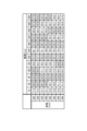
- the transmittance (%) for each combination of the thickness of the protective film 60 and the wavelength of light is, for example, as shown in Figure 10.
- the example in Figure 10 shows the wavelength of red light (625 to 660 nm), which is a visible light that is often used in sensors.
- the thickness of the protective film 60 is in the range of 20 to 200 nm and 300 to 600 nm, the transmittance is below 50% for light of any wavelength. Therefore, when the protective film 60 is made of polysilicon, it is preferable that the thickness is within the range of 20 to 200 nm and 300 to 600 nm.
- the transmittance (%) for each combination of protective film 60 thickness and light wavelength is, for example, as shown in FIG. 11. Referring to FIG. 11, for the entire range of film thicknesses from 40 to 600 nm, the transmittance for light of any wavelength from 625 to 660 nm is below 50%. Therefore, when the protective film 60 is made of amorphous silicon, the position of the glass substrate W can be detected if the film thickness is between 40 and 600 nm.
- the glass substrate W since the glass substrate W is an insulator, it cannot be attracted to an electrostatic chuck by electrostatic force.
- the protective film 60 which is a silicon-containing film, it may be possible to attract the glass substrate W on which the protective film 60 is formed to an electrostatic chuck.
- a protective film 60 having a thickness of 500 nm or more is formed on the second surface W2 of the glass substrate W, it becomes possible to attract the glass substrate W to an electrostatic chuck. This makes it possible to attract the glass substrate W to an electrostatic chuck without having to separately form a conductive film on the glass substrate W.
- the protective film 60 which is a silicon-containing film, may be doped with impurities other than silicon.
- impurities include phosphorus, boron, arsenic, antimony, aluminum, and gallium.
- the conductivity of the protective film 60 can be increased, so that even if the protective film 60 is thinner, the glass substrate W can be attracted to the electrostatic chuck.
- the silicon-containing film is formed of amorphous silicon, polysilicon, or silicon doped with at least one of phosphorus and boron.
- the silicon-containing film is formed of polysilicon; 5.
- the silicon-containing film formed on the first surface and the second surface of the glass substrate has a thickness of 20 nm or more and 200 nm or less, or 300 nm or more and 600 nm or less.
- the silicon-containing film is formed of amorphous silicon; 5.
- the silicon-containing film formed on the first surface and the second surface of the glass substrate has a thickness of 20 nm or more and 600 nm or less.
- Appendix 7 The substrate processing method according to claim 1, wherein in the step a), the silicon-containing film formed on the first surface and the second surface of the glass substrate has a thickness of 500 nm or more.
- Appendix 8) 8. The substrate processing method according to claim 1, wherein in the step a), the silicon-containing film is also formed on a side surface of the glass substrate.
- the silicon-containing film formed on the first surface and the second surface of the glass substrate has a thickness of 600 nm or less.
Landscapes
- Chemical & Material Sciences (AREA)
- General Chemical & Material Sciences (AREA)
- Chemical Kinetics & Catalysis (AREA)
- Engineering & Computer Science (AREA)
- Materials Engineering (AREA)
- Organic Chemistry (AREA)
- Mechanical Engineering (AREA)
- Metallurgy (AREA)
- Inorganic Chemistry (AREA)
- Life Sciences & Earth Sciences (AREA)
- Geochemistry & Mineralogy (AREA)
- Surface Treatment Of Glass (AREA)
Abstract
基板処理方法は、工程a)と、工程b)とを含む。工程a)では、ガラス基板の第1面および第1面の裏面である第2面に、シリコン含有膜が形成される。工程b)では、第1面に形成されたシリコン含有膜が除去される。
Description
本開示の種々の側面および実施形態は、基板処理方法および基板処理システムに関する。
例えば下記の特許文献1には、「複数の切り出された薄板ガラス基板を組み合わせて導光板として用いられる場合、典型的には、切り出された薄板ガラス基板は積層して導光板として用いられる。導光体は、例えば、ヘッドマウントディスプレイなどの表示装置などに適用される。」ことが開示されている。
本開示は、ガラス基板に対して成膜やエッチングなどの処理を行うことができる基板処理方法および基板処理システムを提供する。
本開示の一側面は、基板処理方法であって、工程a)と、工程b)とを含む。工程a)では、ガラス基板の第1面および第1面の裏面である第2面に、シリコン含有膜が形成される。工程b)では、第1面に形成されたシリコン含有膜が除去される。
本開示の種々の側面および実施形態によれば、処理対象がガラス基板であることに起因する一つまたは複数の課題を克服して、ガラス基板に対して成膜やエッチングなどの処理を行うことができる。
以下に、開示される基板処理方法および基板処理システムの実施形態について、図面に基づいて詳細に説明する。なお、以下の実施形態により、開示される基板処理方法および基板処理システムが限定されるものではない。
近年、AR(Augmented Reality)グラス等の高機能の光学素子を製造するために、ガラス基板を用いた微細加工の技術が用いられている。微細加工では、ガラス基板に対してエッチングや成膜等の処理が行われる。
また、市販のガラス基板は、製造の過程で用いられた金属元素が表面に付着している場合がある。そのため、市販のガラス基板をそのまま用いて処理装置によりエッチングや成膜等の処理が行われると、ガラス基板と接触する処理装置内の部材が金属元素で汚染される場合がある。処理装置内の部材が金属元素で汚染されると、ガラス基板に対するエッチングや成膜の過程で、金属元素が混入し、光学素子の欠陥となってしまう場合がある。
本開示は、ガラス基板による処理装置内の金属汚染を抑制することができる側面を有する。
(第1の実施形態)
[基板処理システム10]
図1は、本開示の一実施形態における基板処理システム10の一例を示すシステム構成図である。本実施形態における基板処理システム10は、制御装置20、成膜装置30、エッチング装置40、および処理装置群50を備える。
[基板処理システム10]
図1は、本開示の一実施形態における基板処理システム10の一例を示すシステム構成図である。本実施形態における基板処理システム10は、制御装置20、成膜装置30、エッチング装置40、および処理装置群50を備える。
成膜装置30は、ガラス基板Wの両面および側面に保護膜を形成することにより、ガラス基板Wの両面および側面を保護膜で覆う。本実施形態において、保護膜は、ポリシリコンやアモルファスシリコン等のシリコン含有膜である。
エッチング装置40は、保護膜で覆われたガラス基板Wにおいて、成膜やエッチング等の処理が行われる面(以下、第1面と記載する)を覆う保護膜を除去する。エッチング装置40は、除去装置の一例である。
処理装置群50は、ガラス基板Wに成膜やエッチング等の処理を施す処理装置を有する。処理装置は、保護膜が除去されたガラス基板Wの第1面に対して、成膜やエッチング等の処理を施す。
制御装置20は、メモリ、プロセッサ、および入出力インターフェイスを有する。メモリ内には、レシピ等のデータやプログラム等が格納される。メモリは、例えばRAM(Random Access Memory)、ROM(Read Only Memory)、HDD(Hard Disk Drive)、またはSSD(Solid State Drive)等である。プロセッサは、CPU(Central Processing Unit)またはDSP(Digital Signal Processor)等である。プロセッサは、メモリから読み出されたプログラムを実行することにより、メモリ内に格納されたレシピ等のデータに基づいて、入出力インターフェイスを介して成膜装置30、エッチング装置40、および処理装置群50の各部を制御する。
[成膜装置30の構成]
図2は、成膜装置30の構成の一例を示す概略断面図である。図2には、成膜装置30の一例としてバッチ式の縦型の熱処理装置が示されている。なお、成膜装置30は、ガラス基板の両面および側面にシリコン含有膜を形成することが可能な装置であれば、枚葉式の成膜装置であってもよい。
図2は、成膜装置30の構成の一例を示す概略断面図である。図2には、成膜装置30の一例としてバッチ式の縦型の熱処理装置が示されている。なお、成膜装置30は、ガラス基板の両面および側面にシリコン含有膜を形成することが可能な装置であれば、枚葉式の成膜装置であってもよい。
成膜装置30は、長手方向が鉛直方向に延在する略円筒状の反応管32を備える。反応管32は、内管33と、内管33を覆うと共に内管33と一定の間隔を有するように形成された有天井の外管34とを含む二重管構造である。内管33および外管34は、例えば石英等の耐熱および耐腐食性に優れた材料により形成されている。
外管34の下方には、ステンレス鋼(SUS)等により筒状に形成されたマニホールド35が配置されている。マニホールド35は、外管34の下端と気密に接続されている。また、内管33は、マニホールド35の内壁から突出すると共に、マニホールド35と一体に形成された支持リング36に支持されている。
マニホールド35の下方には蓋体37が配置されている。蓋体37は、ボートエレベータ38により上下動可能に構成されている。ボートエレベータ38により蓋体37が上昇すると、マニホールド35の下方側(炉口部分)が閉鎖される。また、ボートエレベータ38により蓋体37が下降すると、マニホールド35の下方側(炉口部分)が開口される。
蓋体37には、例えば石英等で形成されたボート39が載置される。ボート39は、ガラス基板Wが反応管32の延在方向に沿って所定の間隔をおいて複数枚収容可能に構成されている。図3は、ボート39の構造の一例を示す図である。
例えば図3に示されるように、ボート39は、天板391と底板392とを備える。天板391と底板392との間に複数本(図3の例では3本)の支柱393が設けられている。支柱393の間には補助柱394が設けられている。また、支柱393には、ガラス基板Wを支持するための爪部393aが予め定められた間隔で設けられている。爪部393aは、ボート39の中心方向に向かって突き出し、天板391および底板392と略平行な面を有するように形成されている。
図4は、ボート39の爪部393a付近の一例を示す拡大断面図である。爪部393aは、爪部393aの上面において、ガラス基板Wのエッジ部分を支持する。これにより、ガラス基板Wの第1面W1、第1面W1の裏面の第2面W2、およびガラス基板Wの側面W3に保護膜60を形成することができる。ガラス基板Wの第1面W1は、光学素子が形成される面である。
図2に戻って説明を続ける。反応管32の周囲には、反応管32を取り囲むように断熱体311が設けられている。断熱体311の内壁面には、例えば抵抗発熱体等のヒータ312が設けられている。ヒータ312により反応管32の内部が予め定められた温度に加熱され、ガラス基板Wが予め定められた温度に加熱される。
マニホールド35の側面には、複数の処理ガスを導入するための配管313が接続されている。具体的には、配管313は、支持リング36より下方(内管33の下方)のマニホールド35の側面に接続されている。配管313は、反応管32内の空間に処理ガスを供給する。なお、図2の例では、配管313が1つ描かれているが、内管33内の空間に供給される処理ガスの種類に応じた数の配管313が接続されてもよい。本実施形態では、ガラス基板Wの表面にシリコン含有膜である保護膜60を形成するため、処理ガスとしては、例えばシランガスが用いられる。
配管313は、図示しないマスフローコントローラ等を介して、図示しない処理ガス供給源に接続されている。これにより、処理ガス供給源から配管313を介して予め定められた量の処理ガスが反応管32内の空間に供給される。
マニホールド35の側面には反応管32内の空間のガスを排気するための排気口314が設けられている。排気口314は支持リング36より上方に設けられており、反応管32内の内管33と外管34との間に形成された空間に連通する。排気口314には排気管316が気密に接続されている。排気管316には、バルブ17および真空ポンプ318が設けられている。バルブ317は、排気管316の開度を調整して、反応管32内の圧力を予め定められた圧力に制御する。真空ポンプ318は、排気管316を介して反応管32内のガスを排気する。
マニホールド35の側面の排気口314の下方には、パージガスを供給するための配管315が挿通されている。配管315には、図示しないパージガス供給源が接続されており、パージガス供給源から配管315を介して予め定められた量のパージガス(例えば窒素ガス)が反応管32内に供給される。
[エッチング装置40の構成]
図5は、エッチング装置40の一例を示す概略断面図である。エッチング装置40は、チャンバ420と、基板保持機構430と、液供給部440と、回収カップ450とを備える。
図5は、エッチング装置40の一例を示す概略断面図である。エッチング装置40は、チャンバ420と、基板保持機構430と、液供給部440と、回収カップ450とを備える。
チャンバ420は、基板保持機構430と液供給部440と回収カップ450とを収容する。チャンバ420の天井部には、FFU(Fan Filter Unit)421が設けられている。FFU421は、チャンバ420内にダウンフローを形成する。
FFU421は、バルブ422を介してガス供給源423に接続される。FFU421は、ガス供給源423から供給されるドライエア等のガスをチャンバ420内に吐出する。
基板保持機構430は、回転保持部431と、支柱部432と、駆動部433とを備える。回転保持部431は、チャンバ420の略中央に設けられる。回転保持部431の上面には、ガラス基板Wを側面から保持する保持部材4311が設けられる。保持部材4311は、第1面W1が上方を向くようにガラス基板Wを保持する。また、保持部材4311は、ガラス基板Wが回転保持部431の上面からわずかに離間した状態でガラス基板Wを水平に保持する。
支柱部432は、鉛直方向に延在する部材であり、基端部が駆動部433によって回転可能に支持され、先端部において回転保持部431を水平に支持する。駆動部433は、支柱部432を鉛直軸まわりに回転させる。
基板保持機構430は、駆動部433を用いて支柱部432を回転させることによって支柱部432に支持された回転保持部431を回転させる。これにより、回転保持部431に保持されたガラス基板Wが回転する。
なお、回転保持部431は、ガラス基板Wを側面から保持するタイプに限られず、例えばバキュームチャックのようにガラス基板Wを下方から吸着保持するタイプであってもよい。
液供給部440は、基板保持機構430に保持されたガラス基板Wに対して各種の処理液を供給する。液供給部440は、複数(図5の例では2つ)のノズル441a、441bと、ノズル441a、441bを水平に支持するアーム442と、アーム442を旋回および昇降させる旋回昇降機構443とを備える。なお、ノズル441aおよびノズル441bは、別々のアームに支持されてもよい。
ノズル441aには、バルブ444aおよび流量調整器446aを介してエッチング液供給源445aが接続される。また、ノズル441bには、バルブ444bおよび流量調整器446bを介してリンス液供給源445bが接続される。
ノズル441aからは、エッチング液供給源445aから供給されるエッチング液が吐出される。本実施形態におけるエッチング液は、例えばTMAH(水酸化テトラメチルアンモニウム)、フッ硝酸、またはフッ硝酸酢酸等である。
ノズル441bからは、リンス液供給源445bから供給されるリンス液が吐出される。リンス液は、例えばDIW(脱イオン水)である。
回収カップ450は、回転保持部431を取り囲むように配置され、回転保持部431の回転によってガラス基板Wから飛散する処理液を捕集する。回収カップ450の底部には、排液口451が形成されており、回収カップ450によって捕集された処理液は、排液口451からエッチング装置40の外部へ排出される。また、回収カップ450の底部には、FFU421から供給されるガスをエッチング装置40の外部へ排出する排気口452が形成される。
なお、エッチング装置40に設けられるノズルの個数は、上記の例に限定されるものではなく、例えば、エッチング液およびリンス液を吐出する単一のノズルを備える構成であってもよい。
保持部材4311によって第1面W1が上方を向くように保持されたガラス基板Wに対して、ノズル441aからエッチング液が供給されることにより、ガラス基板Wの第1面W1に形成されていた保護膜60が除去される。この際、ガラス基板Wの第2面W2および側面W3に形成されていた保護膜60は除去されずに残る。
[処理装置群50の構成]
図6は、処理装置群50の一例を示す平面図である。図6では、便宜的に一部の装置の内部の構成要素が透過するように描かれている。処理装置群50は、真空搬送室51、複数の処理装置52、複数のロードロック室53、および大気搬送室54を備える。真空搬送室51は、搬送室の一例である。
図6は、処理装置群50の一例を示す平面図である。図6では、便宜的に一部の装置の内部の構成要素が透過するように描かれている。処理装置群50は、真空搬送室51、複数の処理装置52、複数のロードロック室53、および大気搬送室54を備える。真空搬送室51は、搬送室の一例である。
真空搬送室51の側壁には、ゲートバルブG1を介して処理装置52が接続されている。なお、図6の例では、真空搬送室51に処理装置52が8台接続されているが、開示の技術はこれに限られない。真空搬送室51に接続される処理装置52の数は、7台以下であってもよく、9台以上であってもよい。
それぞれの処理装置52には、第1面W1に形成されていた保護膜60がエッチング装置40によって除去されたガラス基板Wが搬入される。そして、それぞれの処理装置52には、ガラス基板Wの第1面W1に対して成膜やエッチング等の処理を施すことにより、ガラス基板Wの第1面W1を加工したり、ガラス基板Wの第1面W1の上に構造物を形成する。
真空搬送室51の他の側壁には、ゲートバルブG2を介して複数のロードロック室53が接続されている。図6の例では、真空搬送室51に2台のロードロック室53が接続されているが、開示の技術はこれに限られない。真空搬送室51に接続されるロードロック室53の数は、1台であってもよく、3台以上であってもよい。
真空搬送室51内には、搬送装置511が配置されている。搬送装置511は、真空搬送室51内に設けられたガイドレール510に沿って真空搬送室51内を移動する。そして、搬送装置511は、処理装置52とロードロック室53との間でガラス基板Wを搬送する。真空搬送室51内は、大気圧よりも低い圧力雰囲気に保たれている。なお、搬送装置511は、真空搬送室51内の予め定められた位置に固定され、真空搬送室51内を移動しない構成であってもよい。
ロードロック室53の1つの側壁には、ゲートバルブG2を介して真空搬送室51が接続されており、他の1つの側壁には、ゲートバルブG3を介して大気搬送室54が接続されている。ゲートバルブG3が設けられた大気搬送室54の側壁と別な大気搬送室54の側壁には、複数のロードポート55が設けられている。それぞれのロードポート55には、複数のガラス基板Wを収容可能なFOUP(Front Opening Unified Pod)等の容器が接続される。なお、大気搬送室54には、ガラス基板Wの向きを変更するアライナモジュール等が設けられてもよい。
大気搬送室54内の圧力は、大気圧である。大気搬送室54内には、搬送装置541が設けられている。搬送装置541は、大気搬送室54内に設けられたガイドレール540に沿って大気搬送室54内を移動し、ロードロック室53とロードポート55に接続された容器との間でガラス基板Wを搬送する。なお、搬送装置541は、大気搬送室54内の予め定められた位置に固定され、大気搬送室54内を移動しない構成であってもよい。
ゲートバルブG1、ゲートバルブG2、ゲートバルブG3、およびロードポート55の近傍には、ガラス基板Wの位置を検出するセンサ56が設けられている。センサ56は、例えば図7に示されるように、発光部56aと受光部56bとを有する。発光部56aは、受光部56bへ向けて赤色等の可視光を放射する。受光部56bは、発光部56aから放射された光を受光したか否かを制御装置20へ出力する。制御装置20は、発光部56aから放射された光がガラス基板Wによって遮られたか否かに基づいて、ガラス基板Wの位置を検出する。
本実施形態におけるガラス基板Wは光を透過するため、センサ56によってガラス基板Wの位置を検出することが難しい。しかし、本実施形態では、ガラス基板Wの表面に保護膜60が形成されるため、保護膜60の厚さによっては、発光部56aから放射された光が保護膜60によって遮られ、センサ56によってガラス基板Wの位置を検出することが可能となる。しかし、保護膜60を厚くし過ぎると、ガラス基板Wと保護膜60との応力の違いによって反り等のガラス基板Wの変形が起こる場合がある。ガラス基板Wの厚さが700μm程度である場合、保護膜の厚さが例えば600nm以上になると、ガラス基板Wが反る場合がある。ガラス基板Wが反ると、処理装置52によってガラス基板Wに処理を施す場合に、ホールやトレンチの位置や形状の精度が低くなる場合がある。そのため、ガラス基板Wには保護膜60をあまり厚く形成しないことが好ましい。しかし、保護膜60が薄すぎると、発光部56aから放射された光が保護膜60を透過してしまう。
ここで、本実施形態では、ガラス基板Wの側面W3にも保護膜60が形成される。また、例えば図7に示されるように、発光部56aは、ガラス基板Wの側面W3に形成された保護膜60に対して、側面W3に沿う方向(ガラス基板Wの厚さ方向)に光を放射する。ガラス基板Wは、700μm以上の厚さがあるため、側面W3の形成されている保護膜60において、側面W3に沿う方向における保護膜60は700μm以上の厚さがある。これにより、ガラス基板Wの第2面W2に保護膜60をそれほど厚く形成しなくても、側面W3に形成された保護膜60によって発光部56aから放射された光を遮ることができる。これにより、本実施形態では、ガラス基板Wの変形を防止しつつ、センサ56によってガラス基板Wの位置を検出することができる。
[基板処理方法]
図8は、第1の実施形態における基板処理方法の一例を示すフローチャートである。図8に例示される処理は、制御装置20が、成膜装置30、エッチング装置40、および処理装置群50の各部を制御することにより実現される。
図8は、第1の実施形態における基板処理方法の一例を示すフローチャートである。図8に例示される処理は、制御装置20が、成膜装置30、エッチング装置40、および処理装置群50の各部を制御することにより実現される。
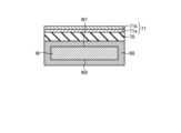
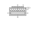
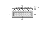
まず、ガラス基板Wに保護膜60が形成される(ステップS10)。ステップS10は、工程a)の一例である。ステップS10では、例えば図9Aに示されるように、ガラス基板Wの第1面W1、第2面W2、および側面W3に、シリコン含有膜である保護膜60が形成される。本実施形態では、成膜装置30によって保護膜60が形成されるため、ガラス基板Wの第1面W1、第2面W2、および側面W3に保護膜60が同時に形成される。ステップS10では、ガラス基板Wが40nm以上かつ600nm以下の厚さの保護膜60で覆われる。
ここで、市販のガラス基板Wは、製造の過程で用いられた金属元素等が表面に付着している場合がある。そのため、市販のガラス基板Wをそのまま用いて処理装置52によりエッチングや成膜等の処理が行われると、ガラス基板Wと接触する処理装置52のチャンバ内の部材が金属元素で汚染される場合がある。チャンバ内の部材が金属元素で汚染されると、ガラス基板Wに対するエッチングや成膜の過程で、金属元素が混入し、光学素子の欠陥となってしまう場合がある。
これに対し、本実施形態では、ステップS10において、ガラス基板Wが40nm以上の厚さの保護膜60で覆われる。これにより、その後のガラス基板Wに対するエッチングや成膜の工程において、ガラス基板Wと接触する処理装置52のチャンバ内の部材等が金属元素で汚染されることを抑制することができる。
また、ステップS10では、ガラス基板Wに形成される保護膜60の厚さが例えば600nm以下に制御される。これにより、ガラス基板Wの変形を抑制することができる。
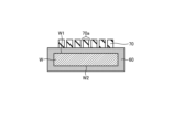
次に、ガラス基板Wの第1面W1に形成された保護膜60が除去される(ステップS11)。ステップS11は、工程b)の一例である。ステップS11では、例えば図9Bに示されるように、エッチング装置40によって、ガラス基板Wの第1面W1に形成された保護膜60が除去され、第1面W1が露出する。
ステップS11では、第2面W2および側面W3は保護膜60で覆われたままとなっている。これにより、ガラス基板Wと接触する処理装置52のチャンバ内の部材(例えばガラス基板Wを載せるステージ)等が金属元素で汚染されることを抑制することができる。また、第2面W2および側面W3の少なくとも一方に形成された保護膜60によって発光部56aから放射された光を遮ることができ、ガラス基板Wの位置を検出することができる。
次に、ガラス基板Wの処理が実行される(ステップS12)。ステップS12は、工程c)の一例である。ステップS12では、例えば図9Cに示されるように、処理装置群50の処理装置52によって、ガラス基板Wに対してエッチングや成膜等の処理が行われ、ガラス基板Wの第1面W1に構造物61が形成される。そして、本フローチャートに示された処理が終了する。
以上、第1の実施形態について説明した。上記したように、第1の実施形態における基板処理方法は、工程a)と、工程b)とを含む。工程a)では、ガラス基板(ガラス基板W)の第1面(第1面W1)および第1面の裏面である第2面(第2面W2)に、シリコン含有膜(保護膜60)が形成される。工程b)では、第1面に形成されたシリコン含有膜が除去される。これにより、ガラス基板による金属汚染を抑制することができる。
また、上記した第1の実施形態において、工程a)では、ガラス基板の第1面および第2面に形成されるシリコン含有膜の膜厚が40nm以上である。これにより、ガラス基板の表面に付着している金属元素の飛散を防止することができる。
また、上記した第1の実施形態において、工程a)では、ガラス基板の第1面および第2面に形成されるシリコン含有膜の膜厚が600nm以下であることが好ましい。これにより、ガラス基板の反りを抑制することができる。
また、上記した第1の実施形態において、シリコン含有膜は、アモルファスシリコンまたはポリシリコンで形成される。これにより、ガラス基板Wの表面を保護膜60で容易に被覆することができると共に、除去工程で保護膜60を容易に除去することができる。
また、上記した第1の実施形態において、工程a)では、ガラス基板の側面(側面W3)にもシリコン含有膜が形成される。これにより、センサ56によってガラス基板Wの位置を検出することができる。
また、上記した第1の実施形態は、基板処理システム10であって、成膜装置(成膜装置30)と、除去装置(エッチング装置40)と、処理装置(処理装置52)とを備える。成膜装置は、ガラス基板の第1面および第1面の裏面である第2面に、シリコン含有膜を形成する、除去装置は、ガラス基板の第1面に形成されたシリコン含有膜を除去する。処理装置は、シリコン含有膜が除去されたガラス基板の第1面に対して、成膜およびエッチングの少なくともいずれかの処理を実行する。これにより、ガラス基板による金属汚染を抑制することができる。
また、上記した第1の実施形態において、基板処理システムは、処理装置に対してガラス基板の搬入および搬出を行う搬送室(真空搬送室51)をさらに備える。搬送室は、ガラス基板を搬送する搬送装置(搬送装置511)と、ガラス基板の位置を検出するセンサ(56)とを有する。成膜装置は、ガラス基板の側面にシリコン含有膜をさらに形成する。センサは、ガラス基板の側面に形成されるシリコン含有膜によって光が遮られるか否かに基づいてガラス基板の位置を検出する。これにより、センサ56によってガラス基板Wの位置を検出することができる。
(第2の実施形態)
第1の実施形態では、ガラス基板Wを保護膜60で覆った後に、光学素子が形成される第1面W1の保護膜60が除去され、保護膜60が除去された第1面W1に光学素子が形成される。これに対し、第2の実施形態では、ガラス基板Wを保護膜60で覆った後に、光学素子が形成される第1面W1に形成された保護膜60を加工することにより、第1面W1に形成された保護膜60の一部が含まれる光学素子が形成される。以下では、第1の実施形態と異なる部分を中心に説明を行う。
第1の実施形態では、ガラス基板Wを保護膜60で覆った後に、光学素子が形成される第1面W1の保護膜60が除去され、保護膜60が除去された第1面W1に光学素子が形成される。これに対し、第2の実施形態では、ガラス基板Wを保護膜60で覆った後に、光学素子が形成される第1面W1に形成された保護膜60を加工することにより、第1面W1に形成された保護膜60の一部が含まれる光学素子が形成される。以下では、第1の実施形態と異なる部分を中心に説明を行う。
[基板処理方法]
図12は、第2の実施形態における基板処理方法の一例を示すフローチャートである。図12に例示される処理は、制御装置20が、成膜装置30、エッチング装置40、および処理装置群50の各部を制御することにより実現される。
図12は、第2の実施形態における基板処理方法の一例を示すフローチャートである。図12に例示される処理は、制御装置20が、成膜装置30、エッチング装置40、および処理装置群50の各部を制御することにより実現される。
まず、ガラス基板Wに保護膜60が形成される(ステップS20)。ステップS20は、工程c)の一例である。ステップS20では、例えば図9Aに示されるように、ガラス基板Wの第1面W1、第2面W2、および側面W3に、シリコン含有膜である保護膜60が形成される。本実施形態では、成膜装置30によって保護膜60が形成されるため、ガラス基板Wの第1面W1、第2面W2、および側面W3に保護膜60が同時に形成される。
次に、シリコン酸化膜が形成される(ステップS21)。ステップS21では、保護膜60で覆われたガラス基板Wが処理装置群50の中の成膜装置内に搬入される。そして、成膜装置内に、原料ガスとしてモノシランガス等のシラン含有ガスが導入され、反応ガスとして酸素ガスまたはオゾンガス等の酸素含有ガスが導入される。これにより、例えば図13Aに示されるように、ガラス基板Wの第1面W1に形成された保護膜60の上に、シリコン酸化膜70が形成される。
なお、シリコン酸化膜70は、CVD(Chemical Vapor Deposition)法以外に、PVD(Physical Vapor Deposition)法、ALD(Atomic Layer Deposition)法、またはスピン塗布等により形成されてもよい。
また、ステップS20において、第1面W1に形成された保護膜60の厚さが、光学素子の形成に必要な厚さに満たない場合、ステップS20とS21との間に、第1面W1に形成された保護膜60の上に、さらに保護膜60を形成する工程が実行されてもよい。第1面W1に形成された保護膜60の上に、さらに保護膜60を形成する工程は、工程e)の一例である。
また、ステップS20において、第1面W1に形成された保護膜60の厚さが、光学素子の形成に必要な厚さよりも大きい場合、ステップS20とS21との間に、第1面W1に形成された保護膜60の厚さを減少させるエッチング工程が実行されてもよい。第1面W1に形成された保護膜60の厚さを減少させるエッチング工程は、工程f)の一例である。
また、ステップS20において、第1面W1に形成された保護膜60の厚さが、光学素子の形成に必要な厚さに満たない場合、ステップS20とS21との間に、第1面W1に形成された保護膜60の上にさらに保護膜60を形成する。そして、形成された保護膜60の厚さが光学素子の形成に必要な厚さとなるまで、保護膜60をエッチングすることにより、保護膜60の厚さを微調整してもよい。
次に、ハードマスクが形成される(ステップS22)。ステップS22では、シリコン酸化膜70が形成されたガラス基板Wが処理装置群50の中の塗布装置内に搬入される。そして、塗布装置によって、シリコン酸化膜70の上にハードマスク形成用の処理液が塗布され、例えば図13Bに示されるように、シリコン酸化膜70の上にスピンオンカーボン膜71aおよびスピンオングラス膜71bを含むハードマスク71が形成される。
なお、図13Bの例では、ハードマスク71にスピンオンカーボン膜71aおよびスピンオングラス膜71bの2つの層が含まれるが、ハードマスク71にはスピンオンカーボン膜71aまたはスピンオングラス膜71bのいずれか一方のみが含まれていてもよい。また、ハードマスク71は、金属含有膜、シリコン酸窒化膜、または裏面反射防止膜等を含んでもよい。
次に、レジスト膜が形成される(ステップS23)。ステップS23では、例えば塗布装置内において、ハードマスク71の上にレジスト膜形成用の処理液が塗布されることにより、ハードマスク71の上にレジスト膜が形成される。そして、レジスト膜が形成されたガラス基板Wが処理装置群50の中の露光装置内に搬入され、レジスト膜に所定のパターンが露光される。そして、レジスト膜に所定のパターンが露光されたガラス基板Wが処理装置群50の中の現像装置内に搬入され、現像される。これにより、例えば図13Cに示されるように、ハードマスク71の上に所定パターンのレジスト膜72が形成される。
レジスト膜72は、例えばEUV(Extreme Ultraviolet)用のフォトレジスト膜である。なお、レジスト膜のパターン形成は、例えば、パターンが形成された型(マスク)をレジスト膜の上に配置し、型を介して紫外線の照射や熱処理等を行い、樹脂のレジスト膜を硬化させることにより行われてもよい。レジスト膜のパターン形成は、ナノインプリントリソグラフィーにより行われてもよい。
次に、ハードマスク71およびシリコン酸化膜70をエッチングする(ステップS24)。ステップS24では、所定パターンのレジスト膜72が形成されたガラス基板Wが処理装置群50の中のエッチング装置内に搬入される。そして、エッチング装置内に、フッ素含有ガス等のエッチングガスを導入することにより、レジスト膜72をマスクとしてハードマスク71がエッチングされる。これにより、例えば図13Dに示されるように、レジスト膜72に対応するパターンがハードマスク71に転写される。
そして、エッチング装置内に、フッ素含有ガス等のエッチングガスを導入することにより、レジスト膜72のパターンが転写されたハードマスク71をマスクとしてシリコン酸化膜70がエッチングされる。これにより、例えば図13Eに示されるように、ハードマスク71に対応するパターンがシリコン酸化膜70に転写される。シリコン酸化膜70のエッチングは、シリコン酸化膜70の開口70aの底部から保護膜60が露出するまで行われる。
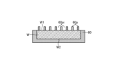
次に、保護膜60がエッチングされる(ステップS25)。ステップS25では、エッチング装置内に、フッ素含有ガス等のエッチングガスを導入することにより、ハードマスク71のパターンが転写されたシリコン酸化膜70をマスクとして、第1面W1に形成された保護膜60がエッチングされる。これにより、例えば図13Fに示されるように、ハードマスク71のパターンに対応した保護膜60のパターン60pが形成される。保護膜60のエッチングは、保護膜60の開口60piの底部からガラス基板Wの第1面W1が露出するまで行われる。ステップS21~S25は、工程d)の一例である。
以上、第2の実施形態について説明した。上記したように、第2の実施形態における基板処理方法は、工程c)と、工程d)とを含む。工程c)では、ガラス基板の第1面および第1面の裏面である第2面に、シリコン含有膜が形成される。工程d)では、第1面に形成されたシリコン含有膜にパターンが形成される。これにより、第1面に形成されたシリコン含有膜にパターンを形成する際のガラス基板による金属汚染を抑制することができる。
また、上記した第2の実施形態における基板処理方法には、工程e)が含まれていてもよい。工程e)は、工程d)の前に実行され、第1面に形成されたシリコン含有膜の厚さを増やすように第1面に形成されたシリコン含有膜の上にさらにシリコン含有膜を形成する。これにより、所望の厚さの保護膜60を含む光学素子を形成することができる。
また、上記した第2の実施形態における基板処理方法には、工程f)が含まれていてもよい。工程f)は、工程d)の前に実行され、第1面に形成されたシリコン含有膜の厚さを減少させるように第1面に形成されたシリコン含有膜をエッチングする。これにより、所望の厚さの保護膜60を含む光学素子を形成することができる。
また、上記した第2の実施形態は、基板処理システム10であって、成膜装置(成膜装置30)と、処理装置(処理装置群50)とを備える。成膜装置は、ガラス基板の第1面および第1面の裏面である第2面に、シリコン含有膜を形成する、処理装置は、第1面に形成されたシリコン含有膜に対して、成膜およびエッチングの少なくともいずれかの処理を実行することにより、第1面に形成されたシリコン含有膜にパターンを形成する。これにより、第1面に形成されたシリコン含有膜にパターンを形成する際のガラス基板による金属汚染を抑制することができる。
[その他]
なお、本願に開示された技術は、上記した実施形態に限定されるものではなく、その要旨の範囲内で数々の変形が可能である。
なお、本願に開示された技術は、上記した実施形態に限定されるものではなく、その要旨の範囲内で数々の変形が可能である。
例えば、上記した各実施形態では、ガラス基板Wの側面W3に形成された保護膜60によって発光部56aから放射された光が遮られるか否かに基づいてガラス基板Wの位置を検出するが、開示の技術はこれに限られない。例えば、600nm以下の範囲内で、ガラス基板Wの第2面W2に保護膜60を厚く形成してもよい。これにより、第2面W2に形成された保護膜60によって発光部56aから放射された光が遮られるか否かに基づいてガラス基板Wの位置を検出することができる。これにより、ガラス基板Wの位置をより容易に検出することができる。
なお、保護膜60の形成に要する時間の短縮やガラス基板Wの反りの防止という観点では、保護膜60は薄い方が好ましい。しかし、保護膜60が薄すぎると、保護膜60の材質によっては、発光部56aから放射された光の透過率が50%を超えてしまう。発光部56aから放射された光の透過率が50%以下であれば、閾値の設定によってはガラス基板Wの位置の検出が可能となる。
保護膜60がポリシリコンである場合、保護膜60の膜厚と光の波長の組み合わせ毎の透過率(%)は、例えば図10のようになる。図10の例では、可視光の中で、センサでよく用いられる赤色の光の波長(625~660nm)について示されている。
図10を参照すると、保護膜60の膜厚が20~200nmおよび300~600nmの範囲では、いずれかの波長の光に対して、透過率が50%を下回っている。従って、保護膜60がポリシリコンである場合には、20~200nmおよび300~600nmの範囲内の膜厚であることが好ましい。
なお、保護膜60がアモルファスシリコンである場合、保護膜60の膜厚と光の波長の組み合わせ毎の透過率(%)は、例えば図11のようになる。図11を参照すると、40~600nmの全範囲の膜厚において、625~660nmのいずれの波長の光の透過率も50%を下回っている。従って、保護膜60がアモルファスシリコンである場合には、40~600nmの膜厚であれば、ガラス基板Wの位置の検出が可能である。
また、ガラス基板Wは、絶縁体であるため、静電気力により静電チャックに吸着させることができない。しかし、シリコン含有膜である保護膜60の膜厚によっては、保護膜60が形成されたガラス基板Wを静電チャックに吸着させることが可能となる。例えば、ガラス基板Wの第2面W2に500nm以上の厚さの保護膜60が形成されると、ガラス基板Wを静電チャックに吸着させることが可能となる。これにより、ガラス基板Wに導電性を有する膜を別途成膜しなくても、ガラス基板Wを静電チャックに吸着させることが可能となる。
また、シリコン含有膜である保護膜60には、シリコン以外の不純物がドープされていてもよい。保護膜60にドープされる不純物としては、例えばリン、ボロン、ヒ素、アンチモン、アルミニウム、またはガリウムなどが挙げられる。不純物の種類によっては保護膜60の導電性を高めることができるので、保護膜60がより薄い場合であっても、ガラス基板Wを静電チャックに吸着させることが可能となる。
なお、今回開示された実施形態は全ての点で例示であって制限的なものではないと考えられるべきである。実に、上記した実施形態は多様な形態で具現され得る。また、上記の実施形態は、添付の請求の範囲およびその趣旨を逸脱することなく、様々な形態で省略、置換、変更されてもよい。
また、上記の各実施形態に関し、さらに以下の付記を開示する。
(付記1)
a)ガラス基板の第1面および前記第1面の裏面である第2面に、シリコン含有膜を形成する工程と、
b)前記第1面に形成された前記シリコン含有膜を除去する工程と
を含む基板処理方法。
(付記2)
前記工程a)では、前記ガラス基板の前記第1面および前記第2面に形成される前記シリコン含有膜の膜厚が40nm以上である付記1に記載の基板処理方法。
(付記3)
前記工程a)では、前記ガラス基板の前記第1面および前記第2面に形成される前記シリコン含有膜の膜厚が600nm以下である付記1または2に記載の基板処理方法。
(付記4)
前記シリコン含有膜は、アモルファスシリコン、ポリシリコン、もしくは、リンまたはボロンの少なくともいずれかが添加されたシリコンで形成される付記1から3のいずれか一つに記載の基板処理方法。
(付記5)
前記シリコン含有膜は、ポリシリコンで形成され、
前記工程a)では、前記ガラス基板の前記第1面および前記第2面に形成される前記シリコン含有膜の膜厚が20nm以上かつ200nm以下、または、300nm以上600nm以下である付記4に記載の基板処理方法。
(付記6)
前記シリコン含有膜は、アモルファスシリコンで形成され、
前記工程a)では、前記ガラス基板の前記第1面および前記第2面に形成される前記シリコン含有膜の膜厚が20nm以上かつ600nm以下である付記4に記載の基板処理方法。
(付記7)
前記工程a)では、前記ガラス基板の前記第1面および前記第2面に形成される前記シリコン含有膜の膜厚が500nm以上である付記1から6のいずれか一つに記載の基板処理方法。
(付記8)
前記工程a)では、前記ガラス基板の側面にも前記シリコン含有膜が形成される付記1から7のいずれか一つに記載の基板処理方法。
(付記9)
ガラス基板の第1面および前記第1面の裏面である第2面に、シリコン含有膜を形成する成膜装置と、
前記ガラス基板の前記第1面に形成された前記シリコン含有膜を除去する除去装置と、
前記シリコン含有膜が除去された前記ガラス基板の前記第1面に対して、成膜およびエッチングの少なくともいずれかの処理を実行する処理装置と
を備える基板処理システム。
(付記10)
前記処理装置に対して前記ガラス基板の搬入および搬出を行う搬送室をさらに備え、
前記搬送室は、
前記ガラス基板を搬送する搬送装置と、
前記ガラス基板の位置を検出するセンサと
を有し、
前記成膜装置は、前記ガラス基板の側面に前記シリコン含有膜をさらに形成し、
前記センサは、前記ガラス基板の第2面および側面の少なくとも一方に形成される前記シリコン含有膜によって光が遮られるか否かに基づいて前記ガラス基板の位置を検出する付記9に記載の基板処理システム。
(付記11)
c)ガラス基板の第1面および前記第1面の裏面である第2面に、シリコン含有膜を形成する工程と、
d)前記第1面に形成された前記シリコン含有膜にパターンを形成する工程と
を含む基板処理方法。
(付記12)
e)前記工程d)の前に実行され、前記第1面に形成された前記シリコン含有膜の厚さを増やすように前記第1面に形成された前記シリコン含有膜の上にさらに前記シリコン含有膜を形成する工程
をさらに含む、付記11に記載の基板処理方法。
(付記13)
f)前記工程d)の前に実行され、前記第1面に形成された前記シリコン含有膜の厚さを減少させるように前記第1面に形成された前記シリコン含有膜をエッチングする工程
をさらに含む、付記11または12に記載の基板処理方法。
(付記14)
前記工程c)では、前記ガラス基板の前記第1面および前記第2面に形成される前記シリコン含有膜の膜厚が40nm以上である付記11から13のいずれか一つに記載の基板処理方法。
(付記15)
前記工程c)では、前記ガラス基板の前記第1面および前記第2面に形成される前記シリコン含有膜の膜厚が600nm以下である付記11から14のいずれか一つに記載の基板処理方法。
(付記16)
前記シリコン含有膜は、アモルファスシリコン、ポリシリコン、もしくは、リンまたはボロンの少なくともいずれかが添加されたシリコンで形成される付記11から15のいずれか一つに記載の基板処理方法。
(付記17)
前記シリコン含有膜は、ポリシリコンで形成され、
前記工程c)では、前記ガラス基板の前記第1面および前記第2面に形成される前記シリコン含有膜の膜厚が20nm以上かつ200nm以下、または、300nm以上600nm以下である付記16に記載の基板処理方法。
(付記18)
前記シリコン含有膜は、アモルファスシリコンで形成され、
前記工程c)では、前記ガラス基板の前記第1面および前記第2面に形成される前記シリコン含有膜の膜厚が20nm以上かつ600nm以下である付記16に記載の基板処理方法。
(付記19)
前記工程c)では、前記ガラス基板の前記第1面および前記第2面に形成される前記シリコン含有膜の膜厚が500nm以上である付記11から18のいずれか一つに記載の基板処理方法。
(付記20)
前記工程c)では、前記ガラス基板の側面にも前記シリコン含有膜が形成される付記11から19のいずれか一つに記載の基板処理方法。
(付記21)
ガラス基板の第1面および前記第1面の裏面である第2面に、シリコン含有膜を形成する成膜装置と、
前記第1面に形成された前記シリコン含有膜に対して、成膜およびエッチングの少なくともいずれかの処理を実行することにより、前記第1面に形成された前記シリコン含有膜にパターンを形成する処理装置と
を備える基板処理システム。
(付記22)
前記処理装置に対して前記ガラス基板の搬入および搬出を行う搬送室をさらに備え、
前記搬送室は、
前記ガラス基板を搬送する搬送装置と、
前記ガラス基板の位置を検出するセンサと
を有し、
前記成膜装置は、前記ガラス基板の側面に前記シリコン含有膜をさらに形成し、
前記センサは、前記ガラス基板の第2面および側面の少なくとも一方に形成される前記シリコン含有膜によって光が遮られるか否かに基づいて前記ガラス基板の位置を検出する付記21に記載の基板処理システム。
G ゲートバルブ
W ガラス基板
W1 第1面
W2 第2面
W3 側面
10 基板処理システム
20 制御装置
30 成膜装置
40 エッチング装置
50 処理装置群
60 保護膜
70 シリコン酸化膜
71 ハードマスク
72 レジスト膜
W ガラス基板
W1 第1面
W2 第2面
W3 側面
10 基板処理システム
20 制御装置
30 成膜装置
40 エッチング装置
50 処理装置群
60 保護膜
70 シリコン酸化膜
71 ハードマスク
72 レジスト膜
Claims (15)
- a)ガラス基板の第1面および前記第1面の裏面である第2面に、シリコン含有膜を形成する工程と、
b)前記第1面に形成された前記シリコン含有膜を除去する工程と
を含む基板処理方法。 - 前記工程a)では、前記ガラス基板の前記第1面および前記第2面に形成される前記シリコン含有膜の膜厚が40nm以上である請求項1に記載の基板処理方法。
- 前記工程a)では、前記ガラス基板の前記第1面および前記第2面に形成される前記シリコン含有膜の膜厚が600nm以下である請求項1または2に記載の基板処理方法。
- 前記シリコン含有膜は、アモルファスシリコン、ポリシリコン、もしくは、リンまたはボロンの少なくともいずれかが添加されたシリコンで形成される請求項1または2に記載の基板処理方法。
- 前記シリコン含有膜は、ポリシリコンで形成され、
前記工程a)では、前記ガラス基板の前記第1面および前記第2面に形成される前記シリコン含有膜の膜厚が20nm以上かつ200nm以下、または、300nm以上600nm以下である請求項4に記載の基板処理方法。 - 前記シリコン含有膜は、アモルファスシリコンで形成され、
前記工程a)では、前記ガラス基板の前記第1面および前記第2面に形成される前記シリコン含有膜の膜厚が20nm以上かつ600nm以下である請求項4に記載の基板処理方法。 - 前記工程a)では、前記ガラス基板の前記第1面および前記第2面に形成される前記シリコン含有膜の膜厚が500nm以上である請求項1または2に記載の基板処理方法。
- 前記工程a)では、前記ガラス基板の側面にも前記シリコン含有膜が形成される請求項1または2に記載の基板処理方法。
- ガラス基板の第1面および前記第1面の裏面である第2面に、シリコン含有膜を形成する成膜装置と、
前記ガラス基板の前記第1面に形成された前記シリコン含有膜を除去する除去装置と、
前記シリコン含有膜が除去された前記ガラス基板の前記第1面に対して、成膜およびエッチングの少なくともいずれかの処理を実行する処理装置と
を備える基板処理システム。 - 前記処理装置に対して前記ガラス基板の搬入および搬出を行う搬送室をさらに備え、
前記搬送室は、
前記ガラス基板を搬送する搬送装置と、
前記ガラス基板の位置を検出するセンサと
を有し、
前記成膜装置は、前記ガラス基板の側面に前記シリコン含有膜をさらに形成し、
前記センサは、前記ガラス基板の第2面および側面の少なくとも一方に形成される前記シリコン含有膜によって光が遮られるか否かに基づいて前記ガラス基板の位置を検出する請求項9に記載の基板処理システム。 - c)ガラス基板の第1面および前記第1面の裏面である第2面に、シリコン含有膜を形成する工程と、
d)前記第1面に形成された前記シリコン含有膜にパターンを形成する工程と
を含む基板処理方法。 - e)前記工程d)の前に実行され、前記第1面に形成された前記シリコン含有膜の厚さを増やすように前記第1面に形成された前記シリコン含有膜の上にさらに前記シリコン含有膜を形成する工程
をさらに含む、請求項11に記載の基板処理方法。 - f)前記工程d)の前に実行され、前記第1面に形成された前記シリコン含有膜の厚さを減少させるように前記第1面に形成された前記シリコン含有膜をエッチングする工程
をさらに含む、請求項11または12に記載の基板処理方法。 - ガラス基板の第1面および前記第1面の裏面である第2面に、シリコン含有膜を形成する成膜装置と、
前記第1面に形成された前記シリコン含有膜に対して、成膜およびエッチングの少なくともいずれかの処理を実行することにより、前記第1面に形成された前記シリコン含有膜にパターンを形成する処理装置と
を備える基板処理システム。 - 前記処理装置に対して前記ガラス基板の搬入および搬出を行う搬送室をさらに備え、
前記搬送室は、
前記ガラス基板を搬送する搬送装置と、
前記ガラス基板の位置を検出するセンサと
を有し、
前記成膜装置は、前記ガラス基板の側面に前記シリコン含有膜をさらに形成し、
前記センサは、前記ガラス基板の第2面および側面の少なくとも一方に形成される前記シリコン含有膜によって光が遮られるか否かに基づいて前記ガラス基板の位置を検出する請求項14に記載の基板処理システム。
Priority Applications (1)
| Application Number | Priority Date | Filing Date | Title |
|---|---|---|---|
| CN202480073297.6A CN122228224A (zh) | 2023-11-27 | 2024-11-13 | 基板处理方法以及基板处理系统 |
Applications Claiming Priority (4)
| Application Number | Priority Date | Filing Date | Title |
|---|---|---|---|
| JP2023199652 | 2023-11-27 | ||
| JP2023-199652 | 2023-11-27 | ||
| JP2024132021 | 2024-08-08 | ||
| JP2024-132021 | 2024-08-08 |
Publications (1)
| Publication Number | Publication Date |
|---|---|
| WO2025115602A1 true WO2025115602A1 (ja) | 2025-06-05 |
Family
ID=95896509
Family Applications (1)
| Application Number | Title | Priority Date | Filing Date |
|---|---|---|---|
| PCT/JP2024/040233 Pending WO2025115602A1 (ja) | 2023-11-27 | 2024-11-13 | 基板処理方法および基板処理システム |
Country Status (2)
| Country | Link |
|---|---|
| CN (1) | CN122228224A (ja) |
| WO (1) | WO2025115602A1 (ja) |
Citations (4)
| Publication number | Priority date | Publication date | Assignee | Title |
|---|---|---|---|---|
| JPH02228043A (ja) * | 1989-02-28 | 1990-09-11 | Hitachi Ltd | 液晶表示装置およびその製造方法 |
| JPH1048245A (ja) * | 1996-08-07 | 1998-02-20 | Nissan Motor Co Ltd | 半導体力学量センサの製造方法 |
| JPH10288580A (ja) * | 1997-04-14 | 1998-10-27 | Olympus Optical Co Ltd | 微小流路素子 |
| JP2002343974A (ja) * | 2001-05-16 | 2002-11-29 | Matsushita Electric Ind Co Ltd | 薄膜トランジスタとその製造方法 |
-
2024
- 2024-11-13 WO PCT/JP2024/040233 patent/WO2025115602A1/ja active Pending
- 2024-11-13 CN CN202480073297.6A patent/CN122228224A/zh active Pending
Patent Citations (4)
| Publication number | Priority date | Publication date | Assignee | Title |
|---|---|---|---|---|
| JPH02228043A (ja) * | 1989-02-28 | 1990-09-11 | Hitachi Ltd | 液晶表示装置およびその製造方法 |
| JPH1048245A (ja) * | 1996-08-07 | 1998-02-20 | Nissan Motor Co Ltd | 半導体力学量センサの製造方法 |
| JPH10288580A (ja) * | 1997-04-14 | 1998-10-27 | Olympus Optical Co Ltd | 微小流路素子 |
| JP2002343974A (ja) * | 2001-05-16 | 2002-11-29 | Matsushita Electric Ind Co Ltd | 薄膜トランジスタとその製造方法 |
Also Published As
| Publication number | Publication date |
|---|---|
| CN122228224A (zh) | 2026-06-16 |
Similar Documents
| Publication | Publication Date | Title |
|---|---|---|
| KR102680084B1 (ko) | 금속-함유 포토레지스트의 재작업 (rework) | |
| US20220344136A1 (en) | Dry chamber clean of photoresist films | |
| TWI896685B (zh) | 光阻的乾式背側及斜角緣部清潔 | |
| US8623765B2 (en) | Processed object processing apparatus, processed object processing method, pressure control method, processed object transfer method, and transfer apparatus | |
| CN112424916B (zh) | 半导体装置的制造方法、基板处理装置和记录介质 | |
| US20200230778A1 (en) | Substrate cleaning device, substrate processing apparatus, substrate cleaning method and substrate processing method | |
| US20100081097A1 (en) | Substrate processing apparatus | |
| KR102676684B1 (ko) | 금속 함유 포토레지스트로부터 금속성 (metallic) 오염의 제어 | |
| EP1630858B1 (en) | Substrate processing system | |
| US20260106122A1 (en) | Dry chamber clean using thermal and plasma processes | |
| TWI425317B (zh) | 光阻塗佈處理方法及光阻圖形之形成方法 | |
| US20260024735A1 (en) | Endpoint detection and tracking of photoresist processes | |
| WO2024196745A1 (en) | Multi-step thermal chamber clean | |
| JP5522903B2 (ja) | 基板乾燥装置およびそれを備えた基板処理装置 | |
| CN120530478A (zh) | 基板处理方法及基板处理系统 | |
| US20090023297A1 (en) | Method and apparatus for hmds treatment of substrate edges | |
| WO2025243875A1 (ja) | 基板処理方法、構造体および成膜装置 | |
| WO2025204318A1 (ja) | 基板処理装置および排気配管洗浄方法 | |
| WO2025064348A1 (en) | Reclamation of hydrogen halides in dry development of photoresists |
Legal Events
| Date | Code | Title | Description |
|---|---|---|---|
| 121 | Ep: the epo has been informed by wipo that ep was designated in this application |
Ref document number: 24897289 Country of ref document: EP Kind code of ref document: A1 |
|
| ENP | Entry into the national phase |
Ref document number: 2025560970 Country of ref document: JP Kind code of ref document: A |
|
| WWE | Wipo information: entry into national phase |
Ref document number: 2025560970 Country of ref document: JP |
|
| NENP | Non-entry into the national phase |
Ref country code: DE |