WO2025100486A1 - 層、光電変換モジュール、層の形成方法及び光電変換モジュールの製造方法 - Google Patents
層、光電変換モジュール、層の形成方法及び光電変換モジュールの製造方法 Download PDFInfo
- Publication number
- WO2025100486A1 WO2025100486A1 PCT/JP2024/039616 JP2024039616W WO2025100486A1 WO 2025100486 A1 WO2025100486 A1 WO 2025100486A1 JP 2024039616 W JP2024039616 W JP 2024039616W WO 2025100486 A1 WO2025100486 A1 WO 2025100486A1
- Authority
- WO
- WIPO (PCT)
- Prior art keywords
- layer
- photoelectric conversion
- groove
- forming
- electrode layer
- Prior art date
- Legal status (The legal status is an assumption and is not a legal conclusion. Google has not performed a legal analysis and makes no representation as to the accuracy of the status listed.)
- Pending
Links
Images







Classifications
-
- B—PERFORMING OPERATIONS; TRANSPORTING
- B23—MACHINE TOOLS; METAL-WORKING NOT OTHERWISE PROVIDED FOR
- B23K—SOLDERING OR UNSOLDERING; WELDING; CLADDING OR PLATING BY SOLDERING OR WELDING; CUTTING BY APPLYING HEAT LOCALLY, e.g. FLAME CUTTING; WORKING BY LASER BEAM
- B23K26/00—Working by laser beam, e.g. welding, cutting or boring
- B23K26/36—Removing material
- B23K26/362—Laser etching
- B23K26/364—Laser etching for making a groove or trench, e.g. for scribing a break initiation groove
-
- H—ELECTRICITY
- H10—SEMICONDUCTOR DEVICES; ELECTRIC SOLID-STATE DEVICES NOT OTHERWISE PROVIDED FOR
- H10F—INORGANIC SEMICONDUCTOR DEVICES SENSITIVE TO INFRARED RADIATION, LIGHT, ELECTROMAGNETIC RADIATION OF SHORTER WAVELENGTH OR CORPUSCULAR RADIATION
- H10F10/00—Individual photovoltaic cells, e.g. solar cells
-
- H—ELECTRICITY
- H10—SEMICONDUCTOR DEVICES; ELECTRIC SOLID-STATE DEVICES NOT OTHERWISE PROVIDED FOR
- H10F—INORGANIC SEMICONDUCTOR DEVICES SENSITIVE TO INFRARED RADIATION, LIGHT, ELECTROMAGNETIC RADIATION OF SHORTER WAVELENGTH OR CORPUSCULAR RADIATION
- H10F10/00—Individual photovoltaic cells, e.g. solar cells
- H10F10/10—Individual photovoltaic cells, e.g. solar cells having potential barriers
- H10F10/16—Photovoltaic cells having only PN heterojunction potential barriers
- H10F10/167—Photovoltaic cells having only PN heterojunction potential barriers comprising Group I-III-VI materials, e.g. CdS/CuInSe2 [CIS] heterojunction photovoltaic cells
-
- H—ELECTRICITY
- H10—SEMICONDUCTOR DEVICES; ELECTRIC SOLID-STATE DEVICES NOT OTHERWISE PROVIDED FOR
- H10F—INORGANIC SEMICONDUCTOR DEVICES SENSITIVE TO INFRARED RADIATION, LIGHT, ELECTROMAGNETIC RADIATION OF SHORTER WAVELENGTH OR CORPUSCULAR RADIATION
- H10F19/00—Integrated devices, or assemblies of multiple devices, comprising at least one photovoltaic cell covered by group H10F10/00, e.g. photovoltaic modules
- H10F19/30—Integrated devices, or assemblies of multiple devices, comprising at least one photovoltaic cell covered by group H10F10/00, e.g. photovoltaic modules comprising thin-film photovoltaic cells
- H10F19/31—Integrated devices, or assemblies of multiple devices, comprising at least one photovoltaic cell covered by group H10F10/00, e.g. photovoltaic modules comprising thin-film photovoltaic cells having multiple laterally adjacent thin-film photovoltaic cells deposited on the same substrate
- H10F19/33—Patterning processes to connect the photovoltaic cells, e.g. laser cutting of conductive or active layers
-
- H—ELECTRICITY
- H10—SEMICONDUCTOR DEVICES; ELECTRIC SOLID-STATE DEVICES NOT OTHERWISE PROVIDED FOR
- H10P—GENERIC PROCESSES OR APPARATUS FOR THE MANUFACTURE OR TREATMENT OF DEVICES COVERED BY CLASS H10
- H10P14/00—Formation of materials, e.g. in the shape of layers or pillars
- H10P14/20—Formation of materials, e.g. in the shape of layers or pillars of semiconductor materials
- H10P14/29—Formation of materials, e.g. in the shape of layers or pillars of semiconductor materials characterised by the substrates
Definitions
- the present invention relates to a layer, a photoelectric conversion module, a method for forming a layer, and a method for manufacturing a photoelectric conversion module.
- a photoelectric conversion module that converts light energy into electrical energy is known (Patent Document 1).
- the photoelectric conversion module described in Patent Document 1 includes a plurality of photoelectric conversion elements arranged adjacent to each other. Each photoelectric conversion element has a conductive substrate, a first electrode layer on the conductive substrate, a photoelectric conversion layer on the first electrode layer, and a second electrode layer on the photoelectric conversion layer.
- a border groove is formed between the first electrode layers of adjacent photoelectric conversion elements.
- a groove is formed between the photoelectric conversion layers of adjacent photoelectric conversion elements.
- the second electrode layer of the photoelectric conversion element is also provided in a part of the groove formed between the photoelectric conversion layers of adjacent photoelectric conversion elements, and is electrically connected to the first electrode layer of the adjacent photoelectric conversion element.
- the second electrode layer (layer) is also formed in the grooves formed between adjacent photoelectric conversion layers to electrically connect the first electrode layer of a photoelectric conversion element to the second electrode layer of an adjacent photoelectric conversion element.
- the layer forming method includes a groove forming step of forming grooves in a base layer along a first direction, and a film forming step of forming a layer on the base layer by physical vapor deposition or chemical vapor deposition while moving the base layer in the first direction.
- the method for manufacturing a photoelectric conversion module includes a first conductive layer forming step of forming a first conductive layer, a step of depositing a photoelectric conversion layer on the first conductive layer to form the base layer, and a second conductive layer forming step of forming a second conductive layer on the base layer.
- the second conductive layer forming step is formed by the above-mentioned layer forming method.
- the layer is formed by the above-mentioned layer formation method.
- the photoelectric conversion module is a photoelectric conversion element manufactured by the above-mentioned method for manufacturing a photoelectric conversion module.
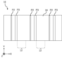
- FIG. 1 is a schematic perspective view of a photoelectric conversion module according to a first embodiment.
- FIG. 2 is a schematic top view of the photoelectric conversion module as viewed in the direction of arrow 2A in FIG.
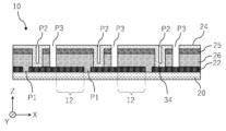
- FIG. 3 is a schematic side view of the photoelectric conversion module as viewed in the direction of arrow 3A in FIG.
- FIG. 4 is a schematic enlarged view of the first conductive layer as viewed in the direction of arrow 4A in FIG.
- FIG. 5 is a schematic enlarged view of the second conductive layer as viewed in the direction of arrow 4A in FIG.
- FIG. 6 is a diagram for explaining the flow of the method for manufacturing the photoelectric conversion module according to the first embodiment.
- FIG. 2 is a schematic top view of the photoelectric conversion module as viewed in the direction of arrow 2A in FIG.
- FIG. 3 is a schematic side view of the photoelectric conversion module as viewed in the direction of arrow 3A in FIG.
- FIG. 4 is a schematic enlarged view of the
- FIG. 7 is a schematic view for explaining one step of the method for manufacturing the photoelectric conversion module according to the first embodiment.
- FIG. 8 is a schematic diagram for explaining a film forming step in the first conductive layer forming process.
- FIG. 9 is a schematic enlarged view of a region 9R in FIG.
- FIG. 10 shows a micrograph of the conductive layer after the deposition step.
- FIG. 11 is a schematic diagram for illustrating a groove forming step (first groove forming step) in the first conductive layer forming process.
- FIG. 12 is a schematic diagram for explaining a state subsequent to FIG.
- FIG. 13 is a schematic diagram for explaining a state subsequent to FIG.
- FIG. 14 is a schematic cross-sectional view taken along line 14A-14A in FIG. FIG.
- FIG. 15 is a schematic side view for explaining the state after the photoelectric conversion layer and the buffer layer are formed.
- FIG. 16 is a schematic diagram for illustrating a step of forming grooves in the photoelectric conversion layer and the buffer layer (second groove forming step).
- FIG. 17 is a schematic cross-sectional view taken along line 17A-17A in FIG.
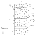
- FIG. 18 is a schematic diagram for explaining a film forming step in the second conductive layer forming process.
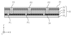
- FIG. 19 is a schematic cross-sectional view taken along line 19A-19A in FIG.
- FIG. 20 is a schematic side view for explaining a state after the film formation step in the second conductive layer formation process.
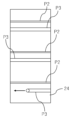
- FIG. 21 is a schematic diagram for illustrating a groove forming step (third groove forming step) in the second conductive layer forming process.
- FIG. 22 is a schematic diagram for explaining a state subsequent to FIG.
- FIG. 23 is a schematic diagram for explaining a state subsequent to FIG.
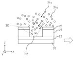
- FIG. 24 is a schematic diagram for explaining a state in which a film is formed while the substrate is moved in a direction (second direction) intersecting the longitudinal direction of the groove in a film forming step in the second conductive layer forming process.
- FIG. 1 is a schematic perspective view of a photovoltaic conversion module according to a first embodiment.
- Fig. 2 is a schematic top view of the photovoltaic conversion module as viewed from the direction of an arrow 2A in Fig. 1.
- Fig. 3 is a schematic side view of the photovoltaic conversion module as viewed from the direction of an arrow 3A in Fig. 1. It should be noted that Figs. 1 to 3 show only a portion of the photovoltaic conversion module.
- the photoelectric conversion module 10 may be, for example, an integrated thin-film photoelectric conversion module.
- the photoelectric conversion module 10 may include a substrate 20 and a plurality of photoelectric conversion elements (cells) 12.
- the plurality of photoelectric conversion elements 12 may be integrated on the substrate 20.
- the photoelectric conversion module 10 is a solar cell module that converts light energy into electrical energy.
- the substrate 20 may be a base on which each film is formed.
- the substrate 20 may be made of, for example, glass, ceramics, resin, or metal.
- Each photoelectric conversion element 12 may have a substantially strip-like shape when viewed from a direction perpendicular to the main surface of the substrate 20.
- Each photoelectric conversion element 12 may extend elongated in a first direction (Y direction in the figure; the same applies below). Furthermore, multiple photoelectric conversion elements 12 are lined up in a second direction (X direction in the figure; the same applies below) that intersects with the first direction.
- Adjacent photoelectric conversion elements 12 may be electrically and/or structurally separated from each other by a first groove P1, a second groove P2, and a third groove P3 that extend in the first direction.
- groove includes both a groove with a bottom and a groove without a bottom.
- the term “groove” also includes a state in which the groove is filled with a material other than the material (layer) in which it is formed.
- Each photoelectric conversion element 12 may include at least a first electrode layer 22, a photoelectric conversion layer 26 on the first electrode layer 22, and a second electrode layer 24 on the photoelectric conversion layer 26.
- the photoelectric conversion layer 26 is provided between the first electrode layer 22 and the second electrode layer 24.
- the first electrode layer 22 is provided on the substrate 20.
- the second electrode layer 24 is located on the opposite side of the photoelectric conversion layer 26 to the substrate 20.
- the first electrode layer (conductive layer) 22 may be made of a conductive metal material or oxide material.
- the metal material can be selected from at least one selected from Ag, Al, Au, Cu, Mo, Ni, Pt, Ti, and Cr, or an alloy thereof.
- the conductive oxide material can be selected from, for example, ITO (indium tin oxide), ITiO (indium titanium oxide), IZO (indium zinc oxide), ZTO (zinc tin oxide), FTO (fluorine doped tin oxide), GZO (gallium doped zinc oxide), etc.
- the second electrode layer (conductive layer) 24 may be made of a conductive metal material or oxide material.
- the metal material can be selected from at least one selected from Ag, Al, Au, Cu, Mo, Ni, Pt, Ti, and Cr, or an alloy thereof.
- the conductive oxide material can be selected from, for example, ITO (indium tin oxide), ITiO (indium titanium oxide), IZO (indium zinc oxide), ZTO (zinc tin oxide), FTO (fluorine doped tin oxide), GZO (gallium doped zinc oxide), etc.
- the first electrode layer 22 may be composed of a transparent electrode layer.
- the substrate 20 is a transparent substrate such as a glass substrate
- the second electrode layer 24 may be a transparent electrode layer or an opaque electrode layer.
- the first electrode layer 22 is composed of a transparent electrode layer, light entering the photoelectric conversion layer 26 or exiting from the photoelectric conversion layer 26 may pass through the substrate 20 and the first electrode layer 22.
- the second electrode layer 24 is formed of an n-type semiconductor, more specifically, a material that has n-type conductivity, a wide band gap, and a relatively low resistance.
- the second electrode layer 24 may be composed of, for example, zinc oxide (ZnO) doped with a group III element or indium tin oxide (ITO). In this case, the second electrode layer 24 can function both as an n-type semiconductor and a transparent electrode layer.
- the photoelectric conversion layer 26 may include, for example, a p-type semiconductor.
- the photoelectric conversion layer 26 is formed of a compound semiconductor including Group I elements (Cu, Ag, Au, etc.), Group III elements (Al, Ga, In, etc.), and Group VI elements (O, S, Se, Te, etc.).
- the photoelectric conversion layer 26 is not limited to the above and may be composed of any material that causes photoelectric conversion.
- the configuration of the photoelectric conversion element 12 is not limited to the above-mentioned embodiment, and can take various forms.
- the photoelectric conversion element 12 may have a configuration in which both an n-type semiconductor and a p-type semiconductor are sandwiched between a first electrode layer and a second electrode layer.
- the second electrode layer does not need to be composed of an n-type semiconductor.
- the photoelectric conversion element 12 is not limited to a p-n bond type structure, and may have a p-i-n bond type structure that includes an intrinsic semiconductor layer (i-type semiconductor) between the n-type semiconductor and the p-type semiconductor.
- the photoelectric conversion element 12 may have a buffer layer 25 between the photoelectric conversion layer 26 and the second electrode layer 24.
- the buffer layer 25 may be a semiconductor material having the same conductivity type as the second electrode layer 24, or may be a semiconductor material having a different conductivity type.
- the buffer layer 25 may be made of a material having a higher electrical resistance than the second electrode layer 24.
- the buffer layer 25 may be a Zn-based buffer layer, a Cd-based buffer layer, or an In-based buffer layer.
- the first electrode layers 22 of adjacent photoelectric conversion elements 12 are electrically separated from each other by the first groove P1.
- the second electrode layers 24 of adjacent photoelectric conversion elements 12 are electrically separated from each other by the third groove P3.
- the photoelectric conversion layers 26 of adjacent photoelectric conversion elements 12 are separated from each other by the second groove P2 and the third groove P3.
- the first groove P1, the second groove P2 and the third groove P3 extend along the first direction.
- the width of the first groove P1 in the second direction may be, for example, in the range of 30 to 200 ⁇ m, preferably in the range of 30 to 100 ⁇ m, and more preferably in the range of 30 to 60 ⁇ m.
- the width of the second groove P2 in the second direction may be, for example, in the range of 30 to 200 ⁇ m, preferably in the range of 30 to 100 ⁇ m, and more preferably in the range of 30 to 60 ⁇ m.
- the width of the third groove P3 in the second direction may be, for example, in the range of 30 to 200 ⁇ m, preferably in the range of 30 to 100 ⁇ m, and more preferably in the range of 30 to 60 ⁇ m.
- the photoelectric conversion module 10 may have electrical connections 34 between adjacent photoelectric conversion elements 12.
- the electrical connections 34 electrically connect adjacent photoelectric conversion elements 12 in series.
- the electrical connections 34 are formed by a portion that extends continuously from the second electrode layer 24.
- the electrical connections 34 are made of the same material as the material that constitutes the second electrode layer 24.
- the electrical connection portion 34 extends in the thickness direction of the photoelectric conversion module 10 at the second groove P2, electrically connecting the first electrode layer 22 of one photoelectric conversion element 12 to the second electrode layer 24 of the other photoelectric conversion element 12.
- FIG. 4 is a schematic enlarged view of the first conductive layer as viewed from the direction of arrow 4A in FIG. 1.
- FIG. 4 shows a schematic view of the shape of the columnar crystals that make up the first electrode layer (first conductive layer) 22.
- the multiple columnar crystals that make up the first electrode layer 22 have a substantially rectangular or ellipsoidal shape that extends long in one direction.
- the long axis direction of the multiple columnar crystals constituting the first electrode layer 22 is oriented at an angle from the direction perpendicular to the surface of the first electrode layer 22.
- the multiple columnar crystals constituting the first electrode layer 22 are oriented at an incline from the direction perpendicular to the surface of the first electrode layer 22 (thickness direction) to a first direction along the surface of the first electrode layer 22.
- the multiple columnar crystals constituting the first electrode layer 22 are oriented at an incline from the direction perpendicular to the surface of the first electrode layer 22 (thickness direction) toward the longitudinal direction of the first groove P1.
- FIG. 5 is a schematic enlarged view of the second conductive layer as viewed from the direction of arrow 4A in FIG. 1.
- FIG. 5 shows a schematic view of the shape of the columnar crystals that make up the second electrode layer (second conductive layer) 24.
- the multiple columnar crystals that make up the second electrode layer 24 have a substantially rectangular or ellipsoidal shape that extends long in one direction.
- the long axis directions of the multiple columnar crystals constituting the second electrode layer 24 are oriented at an angle from the direction perpendicular to the surface of the second electrode layer 24.
- the multiple columnar crystals constituting the second electrode layer 24 are oriented at an incline from the direction perpendicular to the surface of the second electrode layer 24 (thickness direction) to a first direction along the surface of the second electrode layer 24.
- the multiple columnar crystals constituting the second electrode layer 24 are oriented at an incline from the direction perpendicular to the surface of the second electrode layer 24 (thickness direction) toward the longitudinal direction of the third groove P3.
- the long axis direction of the multiple columnar crystals constituting the first electrode layer 22 and the second electrode layer 24 is tilted from the thickness direction toward the longitudinal direction of the first groove P1 and the third groove P3, respectively.
- the long axis direction of the columnar crystals of at least one of the first conductive layer 22 and the second conductive layer 24 may be tilted toward the longitudinal direction of the first groove P1 or the third groove P3.
- the photoelectric conversion module 10 may have wiring (not shown) for extracting power from the photoelectric conversion module 10.
- the photoelectric conversion module 10 may also have a sealing material (not shown) for sealing the first electrode layer 22, the photoelectric conversion layer 26, the buffer layer 25, and the second electrode layer 24.
- FIG. 6 is a diagram for explaining the flow of the method for manufacturing a photoelectric conversion module according to the first embodiment.
- the method for manufacturing a photoelectric conversion module may include a first conductive layer forming step S1, a photoelectric conversion layer forming step S2, a buffer layer forming step S3, and a second conductive layer forming step S4.
- FIG. 7 is a schematic diagram for explaining one step of the manufacturing method of the photoelectric conversion module according to the first embodiment.
- FIG. 8 is a schematic diagram for explaining a film forming step in the first conductive layer forming step.
- FIG. 9 is a schematic enlarged view of a region 9R in FIG. 8.
- FIG. 10 is a diagram showing a microscope photograph of the conductive layer after the film forming step.
- FIG. 11 is a schematic diagram for explaining a groove forming step (first groove forming step) in the first conductive layer forming step.
- FIG. 12 is a schematic diagram for explaining a state subsequent to FIG. 11.
- FIG. 13 is a schematic diagram for explaining a state subsequent to FIG. 12.
- FIG. 14 is a schematic cross-sectional view taken along line 14A-14A in FIG. 11.
- the first conductive layer forming process S1 may include a film forming step S1a followed by a first groove forming step S1b.
- a first electrode layer (first conductive layer) 22 is formed on the substrate 20.
- a first electrode layer (first conductive layer) 22 is formed on the substrate 20 while the substrate 20 is moved in a first direction.
- the movement of the substrate 20 in the first direction can be achieved, for example, by moving a stage on which the substrate 20 is placed.
- the first electrode layers 22 of the multiple photoelectric conversion elements 12 are formed on the substrate 20 in a batch.
- the substrate 20 By depositing a film while moving the substrate 20, the substrate 20 can be moved to the next manufacturing unit while the film is being deposited. This has the advantage of allowing photovoltaic conversion modules to be mass-produced.
- the material constituting the first electrode layer 22 preferably includes a metal material or an oxide material.
- the metal material can be selected from at least one selected from Ag, Al, Au, Cu, Mo, Ni, Pt, Ti, and Cr, or an alloy thereof.
- the conductive oxide material can be selected from, for example, ITO (indium tin oxide), ITiO (indium titanium oxide), IZO (indium zinc oxide), ZTO (zinc tin oxide), FTO (fluorine doped tin oxide), GZO (gallium doped zinc oxide), etc.
- the first electrode layer 22 can be formed by a physical vapor deposition (PVD) method, a chemical vapor deposition (CVD) method, or the like.
- the physical vapor deposition method can be selected from a sputtering method, a vacuum deposition method, an ion plating method, or the like.
- the sputtering method can be a direct current (DC) sputtering method or a radio frequency (RF) sputtering method.
- the chemical vapor deposition method can be selected from a thermal CVD method, a plasma CVD method, an ALD (atomic layer deposition) method, a MOCVD (metal organic chemical vapor deposition) method, or the like.
- the movement speed of the substrate 20 in the first direction may be, for example, in the range of 2 to 60 mm/s, preferably in the range of 30 to 60 mm/s, and more preferably in the range of 45 to 60 mm/s.
- particles 22s constituting the metal material or oxide material rain down on the moving substrate 20 (see FIG. 8).
- particles 22s heading toward the surface of the substrate 20 rain down in a direction (diagonal direction) inclined from a direction perpendicular to the surface of the substrate 20 to the first direction.
- the multiple columnar crystals 22a formed on the substrate 20 are considered to be oriented with an inclination from a direction (thickness direction) perpendicular to the surface of the first electrode layer 22 to the first direction along the surface of the first electrode layer 22, as described above (see also FIGS. 9 and 10).
- Figure 10 shows a micrograph of the first electrode layer 22 after the film formation step, showing how multiple columnar crystals 22a of the first electrode layer 22 formed on the substrate 20 are oriented with an inclination from the thickness direction to the first direction.
- the movement speed of the substrate 20 in the film formation step was low, so the inclination of the columnar crystals 22a is small. It is believed that if the film is formed while moving the substrate 20 at a faster speed, the inclination of the columnar crystals 22a will be greater.
- a first groove P1 is formed along the first direction in the first electrode layer 22 formed in the film formation step S1a (FIGS. 11 to 14). That is, the first groove P1 extends along the movement direction of the substrate 20 in the film formation step S1a.
- the first groove P1 divides the first electrode layer 22 formed in the film formation step S1a into a plurality of regions corresponding to each of the photoelectric conversion elements 12.
- the first groove P1 is preferably formed by a laser or a mechanical blade.
- the substrate 20 may be moved in the first direction while the laser irradiation position or the mechanical blade position SP is kept stationary.
- the laser irradiation position or the mechanical blade position SP may be moved in the first direction while the substrate 20 is kept stationary.
- the multiple first grooves P1 may be formed in sequence while moving the laser irradiation position or the mechanical blade position SP and the substrate 20 back and forth relative to each other along the first direction.
- the first groove P1 is formed so that the width of the first groove P1 is, for example, in the range of 30 to 200 ⁇ m, preferably in the range of 30 to 100 ⁇ m, and more preferably in the range of 30 to 60 ⁇ m.
- the multiple columnar crystals 22a constituting the first electrode layer 22 are considered to be oriented with an inclination from the thickness direction to the first direction (see also Figures 9 and 10).
- the boundaries 22b of the columnar crystals are inclined in the first direction on the side surface viewed from the second direction.
- the first groove P1 is formed along the second direction, since the boundaries 22b of the columnar crystals at both ends of the first groove P1 in the first direction are inclined in the first direction, processing defects are likely to occur at both ends of the first groove P1, and both ends of the first groove P1 are difficult to form neatly straight.
- the first groove P1 is formed along the first direction.
- the boundaries 22b of the columnar crystals at both ends of the first groove P1 in the second direction are hardly inclined in the second direction, so processing defects at both ends of the first groove P1 are suppressed, and both ends of the first groove P1 are easily formed neatly straight.
- the first groove P1 can be formed with high processing quality.
- Step S2 of forming photoelectric conversion layer the photoelectric conversion layer 26 is formed on the first electrode layer 22 with the first groove P1 formed in.
- the photoelectric conversion layer 26 is formed by forming a thin-film precursor layer and then chalcogenizing the precursor layer.
- Methods for forming a precursor layer on the first electrode layer 22 include, for example, sputtering, vapor deposition, and ink coating.
- Vapor deposition is a method for forming a film using atoms that have become gaseous by heating a vapor deposition source.
- Ink coating is a method for dispersing a powder of precursor film material in a solvent such as an organic solvent and coating it on the first electrode layer 22, and then evaporating the solvent to form a precursor layer.
- the precursor layer includes a group I element and a group III element.
- the precursor layer may include Ag as a group I element.
- the group I elements other than Ag included in the precursor layer may be selected from copper, gold, etc.
- the group III elements included in the precursor layer may be selected from indium, gallium, aluminum, etc.
- the precursor layer may also include an alkali metal such as Li, Na, K, Rb, or Cs.
- the precursor layer may also include tellurium as a group VI element in addition to selenium and sulfur.
- the precursor layer is heat-treated in an atmosphere containing a group VI element to chalcogenize it, and the photoelectric conversion layer 26 is formed.
- selenization is first performed by a gas-phase selenization method.
- Selenization is performed by heating the precursor layer in an atmosphere of a selenium source gas (e.g., hydrogen selenide or selenium vapor) that contains selenium as a group VI element source.
- a selenium source gas e.g., hydrogen selenide or selenium vapor
- the precursor layer is converted into a compound (photoelectric conversion layer 26) containing a group I element, a group III element, and selenium.
- the compound (photoelectric conversion layer 26) containing a group I element, a group III element, and selenium may be formed by a method other than the gas-phase selenization method.
- such a compound can also be formed by a solid-phase selenization method, a vapor deposition method, an ink application method, an electrodeposition method, or the like.
- the photoelectric conversion layer 26 containing group I elements, group III elements, and selenium is sulfurized.
- the sulfurization is performed by heating the photoelectric conversion layer 26 in an atmosphere of a sulfur-containing sulfur source gas (e.g., hydrogen sulfide or sulfur vapor).
- a sulfur-containing sulfur source gas e.g., hydrogen sulfide or sulfur vapor.
- the sulfur source gas serves to replace selenium with sulfur in crystals consisting of group I elements, group III elements, and selenium, for example, chalcopyrite crystals, on the surface portion of the photoelectric conversion layer 26.
- a CIS-based photoelectric conversion module has been described as an example of the deposition of the photoelectric conversion layer 26.
- a photoelectric conversion layer 26 having a different layer structure may be deposited.
- the deposition of the photoelectric conversion layer 26 may be appropriately selected according to the layer structure.
- the buffer layer 25 is formed on the photoelectric conversion layer 26.
- the buffer layer 25 can be formed by, for example, a CBD (Chemical Bath Deposition) method or a sputtering method.
- the material constituting the buffer layer 25 is as described above.
- the formation of the buffer layer 25 may be omitted.
- FIG. 15 is a schematic side view for explaining the state after the photoelectric conversion layer and buffer layer are formed.
- a structure (underlying layer) as shown in FIG. 15 is obtained.
- FIG. 15 shows the state as seen from the direction corresponding to the arrow 3A in FIG. 1, i.e., the same direction as FIG. 3.
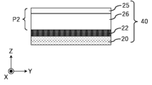
- FIG. 16 is a schematic diagram for explaining a step of forming grooves in the photoelectric conversion layer and the buffer layer (second groove forming step).
- FIG. 17 is a schematic cross-sectional view taken along line 17A-17A in FIG. 16.
- FIG. 18 is a schematic diagram for explaining a film forming step in the second conductive layer forming step.
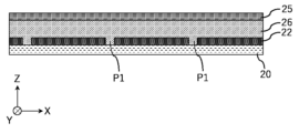
- FIG. 19 is a schematic cross-sectional view taken along line 19A-19A in FIG. 18.
- FIG. 20 is a schematic side view for explaining a state after the film forming step in the second conductive layer forming step.
- FIG. 21 is a schematic diagram for explaining a groove forming step (third groove forming step) in the second conductive layer forming step.
- FIG. 22 is a schematic diagram for explaining a state subsequent to FIG. 21.
- FIG. 23 is a schematic diagram for explaining a state subsequent to FIG. 22.
- the second conductive layer forming step S4 may include a second groove forming step S4a, a film forming step S4b, and a third groove forming step S4c.
- a second groove P2 is formed along the first direction in the laminate including the substrate 20, the first electrode layer 22, the photoelectric conversion layer 26, and the buffer layer 25 (see FIG. 16).
- the laminate including the substrate 20, the first electrode layer 22, the photoelectric conversion layer 26, and the buffer layer 25, and the laminate including the substrate 20, the first electrode layer 22, and the photoelectric conversion layer 26 may be referred to as the "underlayer" (the same applies below).
- the underlayer is not limited to the laminate having the above configuration, and may have any configuration as long as it is a layer that serves as a base for forming the second electrode layer (second conductive layer) 24.
- the underlayer is indicated by the reference symbol 40 in the figure.
- second grooves P2 are formed along the first direction in the photoelectric conversion layer 26 and the buffer layer 25. It is preferable that the second grooves P2 reach the surface of the first electrode layer 22 in the thickness direction.
- the second grooves P2 divide the photoelectric conversion layer 26 and the buffer layer 25 into multiple regions corresponding to each photoelectric conversion element 12.
- the second groove P2 is preferably formed by a laser or a mechanical blade.
- the base layer 40 may be moved in the first direction while the laser irradiation position or the mechanical blade position SP is kept stationary.
- the laser irradiation position or the mechanical blade position SP may be moved in the first direction while the base layer 40 is kept stationary.
- the second groove P2 be formed by a mechanical blade.
- the second groove P2 is formed so that the width of the second groove P2 is in the range of, for example, 30 to 200 ⁇ m, preferably in the range of 30 to 100 ⁇ m, and more preferably in the range of 30 to 60 ⁇ m.
- the multiple second grooves P2 may be formed sequentially while moving the laser irradiation position or the mechanical blade position SP and the base layer 40 back and forth relative to each other along the first direction.
- a second electrode layer 24 (second conductive layer) is deposited on the underlayer 40.
- the second electrode layer (second conductive layer) 24 is deposited on the underlayer 40 while the underlayer 40 is moved in the first direction.
- the movement of the underlayer 40 in the first direction can be achieved, for example, by moving the stage on which the underlayer 40, specifically the substrate 20, is placed.
- the second electrode layers 24 of the multiple photoelectric conversion elements 12 are deposited collectively on the underlayer 40.
- the substrate 20 By depositing the underlayer 40 while moving it, the substrate 20 can be moved to the next manufacturing unit while the film is being deposited. This has the advantage of allowing photovoltaic conversion modules to be mass-produced.
- the material constituting the second electrode layer 24 preferably includes a metal material or an oxide material.
- the metal material can be selected from at least one selected from Ag, Al, Au, Cu, Mo, Ni, Pt, Ti, and Cr, or an alloy thereof.
- the conductive oxide material can be selected from, for example, ITO (indium tin oxide), ITiO (indium titanium oxide), IZO (indium zinc oxide), ZTO (zinc tin oxide), FTO (fluorine doped tin oxide), GZO (gallium doped zinc oxide), etc.
- the second electrode layer 24 can be formed by a PVD method, a CVD method, or the like.
- the PVD method can be selected from a sputtering method, a vacuum deposition method, an ion plating method, or the like.
- the sputtering method can be a DC sputtering method or an RF sputtering method.
- the CVD method can be selected from a thermal CVD method, a plasma CVD method, an ALD method, a MOCVD method, or the like.
- the particles 24s constituting the metal material or oxide material will rain down on the moving underlayer 40. Therefore, the particles 24s heading toward the surface of the underlayer 40 will rain down in a direction (diagonal direction) inclined from a direction perpendicular to the surface of the underlayer 40 to the first direction.
- the multiple columnar crystals 24a formed on the underlayer 40 are considered to be oriented with an inclination from a direction (thickness direction) perpendicular to the surface of the second electrode layer 24 to the first direction along the surface of the second electrode layer 24, as described above (see also FIG. 5).
- FIG. 24 is a schematic diagram for explaining the state in which a film is formed while moving the substrate in a direction (second direction) intersecting the longitudinal direction of the second groove P2 in the film formation step S4b in the second conductive layer formation process S4.
- Particles 24s constituting the metal material or oxide material fall in a direction (diagonal direction) inclined from a direction perpendicular to the surface of the underlayer 40 to the second direction during physical vapor deposition or chemical vapor deposition.
- the region SD of the second groove P2 shown in FIG. 24 is shielded by the photoelectric conversion layer 26 and the buffer layer 25 adjacent to the second groove P2, so that the particles constituting the metal material or oxide material are unlikely to adhere to the region SD.
- the second electrode layer (second conductive layer) 24 is more reliably formed inside the second groove P2. This allows the aforementioned electrical connection portion 34 to be more reliably formed (see also Figure 20). Therefore, it is possible to reduce the possibility of poor electrical connection between the second electrode layer 24 of a certain photoelectric conversion element 12 and the first electrode layer 22 of an adjacent photoelectric conversion element 12.
- the movement speed of the undercoat layer 40 in the first direction may be, for example, in the range of 2 to 60 mm/s, preferably in the range of 30 to 60 mm/s, and more preferably in the range of 45 to 60 mm/s.
- a third groove P3 is formed along the first direction in the second electrode layer 24 formed in the film formation step S4b (FIGS. 21 to 23). That is, the third groove P3 extends along the movement direction of the substrate 20 in the film formation step S4b.
- the third groove P3 divides the second electrode layer 24 formed in the film formation step S4b into multiple regions corresponding to each of the photoelectric conversion elements 12.
- the third groove P3 is preferably formed by a laser or a mechanical blade.
- the substrate 20 may be moved in the first direction while the laser irradiation position or the mechanical blade position SP is kept stationary.
- the laser irradiation position or the mechanical blade position SP may be moved in the first direction while the substrate 20 is kept stationary.
- the multiple third grooves P3 may be formed sequentially while the laser irradiation position or the mechanical blade position SP and the substrate 20 are moved back and forth relative to each other along the first direction.
- the third groove P3 is formed so that the width of the third groove P3 is, for example, in the range of 30 to 200 ⁇ m, preferably in the range of 30 to 100 ⁇ m, and more preferably in the range of 30 to 60 ⁇ m.
- the multiple columnar crystals 24a and columnar crystal boundaries 24b constituting the second electrode layer 24 are considered to be oriented at an angle from the thickness direction to the first direction, similar to the multiple columnar crystals 24a and columnar crystal boundaries 24b constituting the first electrode layer 22 (see also FIG. 5).
- the third groove P3 is formed along the first direction in this state, it is easy to form both ends of the third groove P3 neatly and straight, as explained for the first electrode layer 22 in the first conductive layer formation process S1.
- the third groove P3 can be formed with high processing quality.
- wiring may be connected to extract power from the photoelectric conversion module 10.
- a sealing material (not shown) may be formed to seal the first electrode layer 22, the photoelectric conversion layer 26, the buffer layer 25, and the second electrode layer 24.
- the contents of the present invention are disclosed by taking the photoelectric conversion module and the manufacturing method of the photoelectric conversion module as an example.
- the second conductive layer forming step S4 more specifically the combination of the second groove forming step S4a and the film forming step S4b, can be applied to any layer forming method. That is, the layer forming method according to one aspect only needs to have a groove forming step of forming a groove along a first direction in the base layer, and a film forming step of forming a layer on the base layer by sputtering or vapor deposition while moving the base layer in the first direction.
- the material of the base layer, the conditions for forming the groove, the material of the layer, the conditions for forming the layer, etc. can be those described in the above embodiment.
- the layer formed on the base layer is not particularly limited, but may be a conductive layer.
- the conductive layer may correspond to either or both of the first conductive layer 22 and the second conductive layer 24 described in the above embodiment.
Landscapes
- Physics & Mathematics (AREA)
- Optics & Photonics (AREA)
- Engineering & Computer Science (AREA)
- Plasma & Fusion (AREA)
- Mechanical Engineering (AREA)
- Photovoltaic Devices (AREA)
Abstract
溝の内部に精度よく成膜することができる層の形成方法を提供する。層の形成方法は、下地層(40)に第1方向(Y方向)に沿った溝(P2)を形成する溝形成ステップと、下地層(40)を上記第1方向に移動させつつ、下地層(40)上に物理気相成長又は化学気相成長により層を成膜する成膜ステップと、を有する。
Description
本発明は、層、光電変換モジュール、層の形成方法及び光電変換モジュールの製造方法に関する。
光エネルギーを電気エネルギーに変換する光電変換モジュールが知られている(特許文献1)。特許文献1に記載の光電変換モジュールは、互いに隣接して配置された複数の光電変換素子を備えている。各々の光電変換素子は、導電性基板と、導電性基板上の第1の電極層と、第1の電極層上の光電変換層と、光電変換層上の第2の電極層と、を有する。
互いに隣接する光電変換素子の第1の電極層どうしの間には、縁切り溝が形成されている。互いに隣接する光電変換素子の光電変換層どうしの間には、溝が形成されている。光電変換素子の第2の電極層は、互いに隣接する光電変換素子の光電変換層どうしの間に形成された溝の一部にも設けられており、隣接する光電変換素子の第1の電極層と電気的に接続されている。
第2の電極層(層)は、ある光電変換素子の第1の電極層とそれに隣接する光電変換素子の第2の電極層とを電気的に接続するため、互いに隣接する光電変換層どうしの間に形成された溝にも形成される。しかしながら、特に溝の幅が狭い場合には、層が、溝の内部に成膜しにくいことがある。
したがって、溝の内部に精度よく成膜された層及び当該層を有する光電変換素子、並びに溝の内部に精度よく成膜することができる層の形成方法及び光電変換モジュールの製造方法が望まれる。
一態様に係る層の形成方法は、下地層に第1方向に沿った溝を形成する溝形成ステップと、前記下地層を前記第1方向に移動させつつ、前記下地層上に物理気相成長又は化学気相成長により層を成膜する成膜ステップと、を有する。
一態様に係る光電変換モジュールの製造方法は、第1導電層を形成する第1導電層形成工程と、前記第1導電層上に光電変換層を成膜して前記下地層を形成する工程と、前記下地層上に第2導電層を形成する第2導電層形成工程と、を有する。前記第2導電層形成工程は、上記の層の形成方法により形成される。
一態様に係る層は、上記の層の形成方法により形成された層である。
一態様に係る光電変換モジュールは、上記の光電変換モジュールの製造方法により製造された光電変換素子である。
以下、図面を参照して、実施形態について説明する。以下の図面において、同一又は類似の部分には、同一又は類似の符号を付している。ただし、図面は模式的なものであり、各寸法の比率等は現実のものとは異なることがあることに留意すべきである。
[光電変換モジュール]
図1は、第1実施形態に係る光電変換モジュールの模式的斜視図である。図2は、図1の矢印2A方向から見た光電変換モジュールの模式的上面図である。図3は、図1の矢印3A方向から見た光電変換モジュールの模式的側面図である。なお、図1~3では、光電変換モジュールの一部のみが示されていることに留意されたい。
図1は、第1実施形態に係る光電変換モジュールの模式的斜視図である。図2は、図1の矢印2A方向から見た光電変換モジュールの模式的上面図である。図3は、図1の矢印3A方向から見た光電変換モジュールの模式的側面図である。なお、図1~3では、光電変換モジュールの一部のみが示されていることに留意されたい。
本実施形態に係る光電変換モジュール10は、例えば集積型の薄膜光電変換モジュールであってよい。光電変換モジュール10は、基板20と、複数の光電変換素子(セル)12と、含んでいてよい。複数の光電変換素子12は、基板20上に集積されて設けられていてよい。好ましくは、光電変換モジュール10は、光エネルギーを電気的エネルギーに変換する太陽電池モジュールである。
基板20は、各膜を成膜するベースとなるものであってよい。基板20は、例えばガラス、セラミックス、樹脂又は金属などによって構成されていてよい。
各々の光電変換素子12は、基板20の主面に直交する方向から見て、実質的に帯状の形状を有していてよい。各々の光電変換素子12は第1方向(図のY方向。以下同様。)に長く延びていてよい。また、複数の光電変換素子12は、第1方向に交差する第2方向(図のX方向。以下同様。)に並んでいる。互いに隣接する光電変換素子12は、第1方向に延びる第1溝P1、第2溝P2及び第3溝P3によって互いに電気的及び/又は構造的に分断されていてよい。
本明細書において、「溝」は、底を有する溝と底を有しない溝の両方を含むものとする。また、「溝」という用語は、溝が形成されている材料(層)とは別の材料によって充填されている状態を含むものとする。
各々の光電変換素子12は、少なくとも、第1電極層22と、第1電極層22上の光電変換層26と、光電変換層26上の第2電極層24と、を含んでいてよい。光電変換層26は、第1電極層22と第2電極層24との間に設けられる。第1電極層22は、基板20上に設けられている。第2電極層24は、光電変換層26に関して基板20とは反対側に位置する。
第1電極層(導電層)22は、導電性を有する金属材料又は酸化物材料によって構成されていてよい。金属材料は、Ag,Al,Au,Cu,Mo,Ni,Pt,Ti及びCrから選択された少なくとも1つ、又はこれらの合金から選択可能である。導電性を有する酸化物材料としては、例えば、ITO(酸化インジウムスズ)、ITiO(酸化インジウムチタン)、IZO(酸化インジウム亜鉛)、ZTO(酸化亜鉛スズ)、FTO(フッ素ドープト酸化スズ)、GZO(ガリウムドープト酸化亜鉛)などから選択可能である。
第2電極層(導電層)24は、導電性を有する金属材料又は酸化物材料によって構成されていてよい。金属材料は、Ag,Al,Au,Cu,Mo,Ni,Pt,Ti及びCrから選択された少なくとも1つ、又はこれらの合金から選択可能である。導電性を有する酸化物材料は、例えばITO(酸化インジウムスズ)、ITiO(酸化インジウムチタン)、IZO(酸化インジウム亜鉛)、ZTO(酸化亜鉛スズ)、FTO(フッ素ドープト酸化スズ)、GZO(ガリウムドープト酸化亜鉛)などから選択可能である。
一例では、第2電極層24は透明電極層によって構成されていてよい。この場合、第1電極層22は、透明電極層であってもよく、不透明な電極層であってもよい。第2電極層24が透明電極層によって構成されている場合、光電変換層26へ入射、又は光電変換層26から出射する光は、第2電極層24を通過すればよい。
別の例では、第1電極層22が透明電極層によって構成されていてよい。この場合、基板20は例えばガラス基板のような透明基板であり、かつ第2電極層24は、透明電極層であってもよく、不透明な電極層であってもよい。第1電極層22が透明電極層によって構成されている場合、光電変換層26へ入射、又は光電変換層26から出射する光は、基板20及び第1電極層22を通過すればよい。
好ましい一例として、第2電極層24は、n型半導体、より具体的には、n型の導電性を有し、禁制帯幅が広く、比較的低抵抗の材料によって形成される。第2電極層24は、例えば、III族元素を添加した酸化亜鉛(ZnO)や、酸化インジウムスズ(Indium Tin Oxide:ITO)によって構成されていてよい。この場合、第2電極層24は、n型半導体と透明電極層の機能を兼ねることができる。
光電変換層26は、例えば、p型の半導体を含んでいてよい。CIS系の光電変換モジュールの一例では、光電変換層26は、I族元素(Cu、Ag、Au等)、III族元素(Al、Ga、In等)及びVI族元素(O、S、Se、Te等)を含む化合物半導体で形成される。この代わりに、光電変換層26は、前述したものに限定されず、光電変換を起こす任意の材料によって構成されていてよい。
光電変換素子12の構成は、上記態様に限定されず、様々な態様をとり得ることに留意されたい。例えば、光電変換素子12は、n型半導体とp型半導体の両方が第1電極層と第2電極層との間に挟まれた構成を有していてもよい。この場合、第2電極層はn型半導体によって構成されていなくてよい。また、光電変換素子12は、p-n結合型の構造に限らず、n型半導体とp型半導体との間に真性半導体層(i型半導体)を含むp-i-n結合型の構造を有していてもよい。
光電変換素子12は、光電変換層26と第2電極層24との間にバッファ層25を有していてもよい。この場合、バッファ層25は、第2電極層24と同じ導電型を有する半導体材料であってもよく、異なる導電型を有する半導体材料であってもよい。バッファ層25は、第2電極層24よりも電気抵抗の高い材料によって構成されていればよい。CIS系の光電変換モジュールの一例では、バッファ層25は、Zn系バッファ層、Cd系バッファ層又はIn系バッファ層であってよい。
互いに隣接する光電変換素子12の第1電極層22は、第1溝P1によって互いに電気的に分断されている。同様に、互いに隣接する光電変換素子12の第2電極層24は、第3溝P3によって互いに電気的に分断されている。互いに隣接する光電変換素子12の光電変換層26は、第2溝P2及び第3溝P3によって互いに分断されている。第1溝P1、第2溝P2及び第3溝P3は、第1方向に沿って延びている。
第2方向における第1溝P1の幅は、例えば30~200μmの範囲、好ましくは30~100μmの範囲、より好ましくは30~60μmの範囲であってよい。第2方向における第2溝P2の幅は、例えば30~200μmの範囲、好ましくは30~100μmの範囲、より好ましくは30~60μmの範囲であってよい。第2方向における第3溝P3の幅は、例えば30~200μmの範囲、好ましくは30~100μmの範囲、より好ましくは30~60μmの範囲であってよい。
光電変換モジュール10は、互いに隣接する光電変換素子12どうしの間に電気接続部34を有していてよい。電気接続部34は、互いに隣接する光電変換素子12どうしを電気的に直列に接続する。本実施形態では、電気接続部34は、第2電極層24から連続して延びた部分によって形成されている。この場合、電気接続部34は、第2電極層24を構成する材料と同じ材料から構成される。
電気接続部34は、第2溝P2のところで光電変換モジュール10の厚み方向に延びることで、一方の光電変換素子12の第1電極層22と他方の光電変換素子12の第2電極層24とを互いに電気的に接続する。
図4は、図1の矢印4Aの方向から見た第1導電層の模式的拡大図である。図4は、第1電極層(第1導電層)22を構成する柱状晶の形状を模式的に示している。本実施形態では、第1電極層22を構成する複数の柱状晶は、一方向に長く延びた略直方体又は略楕円体の形状を有する。
第1電極層22を構成する複数の柱状晶の長軸方向は、第1電極層22の表面に直交する方向から角度を付けて配向している。具体的には、第1電極層22を構成する複数の柱状晶は、第1電極層22の表面に直交する方向(厚み方向)から第1電極層22の表面に沿った第1方向に傾斜して配向している。言い換えると、第1電極層22を構成する複数の柱状晶は、第1電極層22の表面に直交する方向(厚み方向)から、第1溝P1の長手方向に向かって傾斜して配向している。
図5は、図1の矢印4Aの方向から見た第2導電層の模式的拡大図である。図5は、第2電極層(第2導電層)24を構成する柱状晶の形状を模式的に示している。本実施形態では、第2電極層24を構成する複数の柱状晶は、一方向に長く延びた略直方体又は略楕円体の形状を有する。
第2電極層24を構成する複数の柱状晶の長軸方向は、第2電極層24の表面に直交する方向から角度を付けて配向している。具体的には、第2電極層24を構成する複数の柱状晶は、第2電極層24の表面に直交する方向(厚み方向)から第2電極層24の表面に沿った第1方向に傾斜して配向している。言い換えると、第2電極層24を構成する複数の柱状晶は、第2電極層24の表面に直交する方向(厚み方向)から、第3溝P3の長手方向に向かって傾斜して配向している。
本実施形態では、第1電極層22及び第2電極層24を構成する複数の柱状晶の長軸方向が、それぞれ、厚み方向から第1溝P1及び第3溝P3の長手方向に向かって傾斜して配向している。この代わりに、第1導電層22と第2導電層24の少なくとも一方の柱状晶の長軸方向が、第1溝P1又は第3溝P3の長手方向に向かって傾斜して配向していてよい。
光電変換モジュール10は、必要に応じて、光電変換モジュール10から電力を取り出す不図示の配線を有していても良い。また、光電変換モジュール10は、第1電極層22、光電変換層26、バッファ層25及び第2電極層24を封止する不図示の封止材を有していても良い。
[層の形成方法及び光電変換モジュールの製造方法]
次に、層の形成方法について説明する。以下では、図6~図23を参照して上記の光電変換モジュールの製造方法を説明しつつ、当該説明のなかで層の形成方法についても説明する。
次に、層の形成方法について説明する。以下では、図6~図23を参照して上記の光電変換モジュールの製造方法を説明しつつ、当該説明のなかで層の形成方法についても説明する。
図6は、第1実施形態に係る光電変換モジュールの製造方法のフローを説明するための図である。光電変換モジュールの製造方法は、第1導電層形成工程S1と、光電変換層を成膜する工程S2と、バッファ層を成膜する工程S3と、第2導電層形成工程S4と、を有していてよい。
(第1導電層形成工程S1)
図7は、第1実施形態に係る光電変換モジュールの製造方法の一工程を説明するための模式図である。図8は、第1導電層形成工程における成膜ステップを説明するための模式図である。図9は、図8の領域9Rの模式的拡大図である。図10は、成膜ステップ後の導電層の顕微鏡写真を示す図である。図11は、第1導電層形成工程における溝形成ステップ(第1溝形成ステップ)を説明するための模式図である。図12は、図11に続く状態を説明するための模式図である。図13は、図12に続く状態を説明するための模式図である。図14は、図11の14A-14A線に沿った模式的断面図である。
図7は、第1実施形態に係る光電変換モジュールの製造方法の一工程を説明するための模式図である。図8は、第1導電層形成工程における成膜ステップを説明するための模式図である。図9は、図8の領域9Rの模式的拡大図である。図10は、成膜ステップ後の導電層の顕微鏡写真を示す図である。図11は、第1導電層形成工程における溝形成ステップ(第1溝形成ステップ)を説明するための模式図である。図12は、図11に続く状態を説明するための模式図である。図13は、図12に続く状態を説明するための模式図である。図14は、図11の14A-14A線に沿った模式的断面図である。
第1導電層形成工程S1は、成膜ステップS1aと、それに続く第1溝形成ステップS1bと、を有していてよい。第1導電層形成工程S1では、基板20上に、第1電極層(第1導電層)22を形成する。
まず、成膜ステップS1aでは、基板20を第1方向に移動させつつ、基板20上に第1電極層(第1導電層)22を成膜する。第1方向への基板20の移動は、例えば基板20を載せたステージを移動させることによって実現できる。複数の光電変換素子12の第1電極層22が、基板20上に一括的に成膜される。
基板20を移動させながら成膜することにより、成膜しつつ次の製造ユニットに基板20を移動させることができる。これにより、光電変換モジュールを大量に製造することができるというメリットが得られる。
第1電極層22を構成する材料は、金属材料又は酸化物材料を含むことが好ましい。金属材料は、Ag,Al,Au,Cu,Mo,Ni,Pt,Ti及びCrから選択された少なくとも1つ、又はこれらの合金から選択可能である。導電性を有する酸化物材料は、例えば、ITO(酸化インジウムスズ)、ITiO(酸化インジウムチタン)、IZO(酸化インジウム亜鉛)、ZTO(酸化亜鉛スズ)、FTO(フッ素ドープト酸化スズ)、GZO(ガリウムドープト酸化亜鉛)などから選択可能である。
第1電極層22の成膜は、物理気相成長(physical vapor deposition:PVD)法、化学気相成長(chemical vapor deposition:CVD)法などにより実施することができる。物理気相成長法としては、スパッタリング法、真空蒸着法、イオンプレーティング法などから選択できる。スパッタリング法は、直流(DC)スパッタリング法でもよいし、高周波(RF)スパッタリング法でもよい。化学気相成長法としては、熱CVD法、プラズマCVD法、ALD(atomic layer deposition)法、MOCVD(Metal Organic Chemical Vapor Deposition)法などから選択できる。
第1方向における基板20の移動速度は、例えば2~60mm/sの範囲、好ましくは30~60mm/sの範囲、より好ましくは45~60mm/sの範囲であってよい。
成膜ステップにおいて、物理気相成長又は化学気相成長中に、金属材料又は酸化物材料を構成する粒子22sは、移動している基板20に降り注ぐことになる(図8参照)。したがって、基板20の表面に向かう粒子22sは、基板20の表面に直交する方向から第1方向に傾斜した方向(斜め方向)に降り注ぐ。これにより、基板20上に成膜された複数の柱状晶22aは、前述したように、第1電極層22の表面に直交する方向(厚み方向)から第1電極層22の表面に沿った第1方向に傾斜して配向すると考えられる(図9及び図10も参照)。
図10は成膜ステップ後の第1電極層22の顕微鏡写真を示しており、基板20上に成膜された第1電極層22の複数の柱状晶22aが、厚み方向から第1方向に傾斜して配向する様子を示している。ここで、図10では、成膜ステップにおける基板20の移動速度が小さかったため、柱状晶22aの傾斜は小さい。より速い速度で基板20を移動させつつ成膜すれば、柱状晶22aの傾斜はより大きくなると考えられる。
次に、第1溝形成ステップS1bにおいて、成膜ステップS1aで成膜された第1電極層22に、上記の第1方向に沿った第1溝P1を形成する(図11~図14)。すなわち、第1溝P1は、成膜ステップS1aにおける基板20の移動方向に沿って延びる。第1溝P1によって、成膜ステップS1aで成膜された第1電極層22は、各々の光電変換素子12に対応する複数の領域に分割される。
第1溝P1は、レーザ又は機械刃によって形成されることが好ましい。第1溝形成ステップS1bでは、レーザの照射位置又は機械刃の位置SPを静止させた状態で、基板20を第1方向に移動させてもよい。この代わりに、基板20を静止させた状態で、レーザの照射位置又は機械刃の位置SPを第1方向に移動させてもよい。
また、図11~図13に示すように、光電変換モジュール10の複数の第1溝P1のそれぞれを順番に形成するため、レーザの照射位置又は機械刃の位置SPと基板20とを第1方向に沿って相対的に往復移動させつつ、複数の第1溝P1を順番に形成してもよい。
第1溝形成ステップS1bにおいて、第1溝P1の幅が例えば30~200μmの範囲、好ましくは30~100μmの範囲、より好ましくは30~60μmの範囲となるように第1溝P1が形成されることが好ましい。
本実施形態において、前述したように、第1電極層22を構成する複数の柱状晶22aは、厚み方向から第1方向に傾斜して配向すると考えられる(図9及び図10も参照)。言い換えると、第2方向から見た側面において柱状晶の境界22bが第1方向に傾斜している。この状態で、仮に第1溝P1が第2方向に沿って形成されるとすると、第1方向における第1溝P1の両端の柱状晶の境界22bが第1方向に傾斜しているため、第1溝P1の当該両端の部分に加工不良が生じやすく、第1溝P1の当該両端部分が綺麗に真っすぐ形成されにくい。一方、本実施形態では、第1溝P1が第1方向に沿って形成される。この場合、第2方向における第1溝P1の両端の柱状晶の境界22bは第2方向にはほとんど傾斜していないため、第1溝P1の当該両端の部分の加工不良が抑制され、第1溝P1の当該両端部分を綺麗に真っすぐ形成し易い。このように、本実施形態によれば、高い加工品質で第1溝P1を形成することができる。
(光電変換層を成膜する工程S2)
次に、第1溝P1が形成された第1電極層22上に、光電変換層26が形成される。CIS系の光電変換モジュールの一例では、光電変換層26は、薄膜状のプリカーサ層を形成した後、当該プリカーサ層をカルコゲン化することで形成される。
次に、第1溝P1が形成された第1電極層22上に、光電変換層26が形成される。CIS系の光電変換モジュールの一例では、光電変換層26は、薄膜状のプリカーサ層を形成した後、当該プリカーサ層をカルコゲン化することで形成される。
第1電極層22上にプリカーサ層を形成する方法としては、例えば、スパッタリング法、蒸着法又はインク塗布法等が挙げられる。蒸着法は、蒸着源を加熱して気相となった原子等を用いて成膜する方法である。インク塗布法は、プリカーサ膜の材料を粉体にしたものを有機溶剤等の溶媒に分散して第1電極層22上に塗布し、その後溶剤を蒸発してプリカーサ層を形成する方法である。
プリカーサ層は、I族元素と、III族元素とを含む。例えば、プリカーサ層はI族元素としてAgを含んでいてもよい。プリカーサ層に含めるAg以外のI族元素は、銅、金などから選択可能である。また、プリカーサ層に含めるIII族元素は、インジウム、ガリウム、アルミニウムなどから選択可能である。また、プリカーサ層は、Li、Na、K、Rb、Cs等のアルカリ金属を含んでいてもよい。また、プリカーサ層は、VI族元素として、セレンおよび硫黄の他に、テルルを含んでいてもよい。
プリカーサ層のカルコゲン化処理では、VI族元素を含む雰囲気中でプリカーサ層を熱処理することでカルコゲン化し、光電変換層26を形成する。例えば、まず、気相セレン化法によるセレン化が行われる。セレン化は、VI族元素源としてセレンを含むセレン源ガス(例えば、セレン化水素またはセレン蒸気)の雰囲気中でプリカーサ層を加熱することにより行う。
その結果、プリカーサ層は、I族元素と、III族元素と、セレンとを含む化合物(光電変換層26)に変換される。なお、I族元素と、III族元素と、セレンとを含む化合物(光電変換層26)は、気相セレン化法以外の方法により形成してもよい。例えば、このような化合物は、固相セレン化法、蒸着法、インク塗布法、電着法などによっても形成可能である。
次に、I族元素と、III族元素と、セレンとを含む光電変換層26の硫化が行われる。硫化は、硫黄を有する硫黄源ガス(例えば、硫化水素又は硫黄蒸気)の雰囲気中で光電変換層26を加熱することにより行う。その結果、光電変換層26は、I族元素と、III族元素と、VI族元素としてセレンおよび硫黄とを含む化合物に変換される。硫黄源ガスは、光電変換層26の表面部において、I族元素と、III族元素と、セレンとからなる結晶、例えば、カルコパイライト結晶内のセレンを硫黄に置換する役割を担う。
光電変換層26の成膜として、CIS系の光電変換モジュールの一例について説明した。この代わりに、別の層構造を有する光電変換層26を成膜してもよい。この場合、光電変換層26の成膜は、当該層構造に応じて適宜選択されればよい。
(バッファ層を成膜する工程S3)
次に、必要に応じて、光電変換層26上に、バッファ層25を成膜する。バッファ層25の成膜は、例えばCBD(Chemical Bath Deposition)法やスパッタリング法などの方法により実施できる。バッファ層25を構成する材料については前述したとおりである。なお、バッファ層25の形成は省略されてもよい。
次に、必要に応じて、光電変換層26上に、バッファ層25を成膜する。バッファ層25の成膜は、例えばCBD(Chemical Bath Deposition)法やスパッタリング法などの方法により実施できる。バッファ層25を構成する材料については前述したとおりである。なお、バッファ層25の形成は省略されてもよい。
図15は、光電変換層及びバッファ層の成膜後の状態を説明するための模式的側面図である。光電変換層26及びバッファ層25の形成により、図15に示すような構造(下地層)が得られる。ここで、図15は、図1の矢印3Aに相当する方向、すなわち図3と同方向から見た状態を示している。
(第2導電層形成工程S4)
図16は、光電変換層及びバッファ層に溝を形成するステップ(第2溝形成ステップ)を説明するための模式図である。図17は、図16の17A-17A線に沿った模式的断面図である。図18は、第2導電層形成工程における成膜ステップを説明するための模式図である。図19は、図18の19A-19A線に沿った模式的断面図である。図20は、第2導電層形成工程における成膜ステップ後の状態を説明するための模式的側面図である。図21は、第2導電層形成工程における溝形成ステップ(第3溝形成ステップ)を説明するための模式図である。図22は、図21に続く状態を説明するための模式図である。図23は、図22に続く状態を説明するための模式図である。
図16は、光電変換層及びバッファ層に溝を形成するステップ(第2溝形成ステップ)を説明するための模式図である。図17は、図16の17A-17A線に沿った模式的断面図である。図18は、第2導電層形成工程における成膜ステップを説明するための模式図である。図19は、図18の19A-19A線に沿った模式的断面図である。図20は、第2導電層形成工程における成膜ステップ後の状態を説明するための模式的側面図である。図21は、第2導電層形成工程における溝形成ステップ(第3溝形成ステップ)を説明するための模式図である。図22は、図21に続く状態を説明するための模式図である。図23は、図22に続く状態を説明するための模式図である。
次に、第2導電層形成工程S4が行われる。第2導電層形成工程S4は、第2溝形成ステップS4aと、成膜ステップS4bと、第3溝形成ステップS4cと、を有していてよい。
第2溝形成ステップS4aでは、基板20、第1電極層22、光電変換層26及びバッファ層25を含む積層体に、第1方向に沿った第2溝P2を形成する(図16参照)。なお、以下では、基板20、第1電極層22、光電変換層26及びバッファ層25を含む積層体、基板20、第1電極層22及び光電変換層26を含む積層体を「下地層」と称することがある(以下、同様)。ただし、下地層は、上記構成の積層体に限られず、第2電極層(第2導電層)24を成膜するための下地(ベース)になる層であれば、どのような構成であってもよい。下地層は、図において符号40で示される。
第2溝形成ステップS4aでは、具体的には、光電変換層26及びバッファ層25に第1方向に沿った第2溝P2を形成する。第2溝P2は、厚み方向において、第1電極層22の表面にまで達することが好ましい。第2溝P2によって、光電変換層26及びバッファ層25は、各々の光電変換素子12に対応する複数の領域に分割される。
第2溝P2は、レーザ又は機械刃によって形成されることが好ましい。第2溝形成ステップS4aでは、レーザの照射位置又は機械刃の位置SPを静止させた状態で、下地層40を第1方向に移動させてもよい。この代わりに、下地層40を静止させた状態で、レーザの照射位置又は機械刃の位置SPを第1方向に移動させてよい。
第2溝P2が第1電極層22に形成されないようにするためには、第2溝P2は、機械刃によって形成されることが好ましい。
第2溝形成ステップS4aにおいて、第2溝P2の幅が例えば30~200μmの範囲、好ましくは30~100μmの範囲、より好ましくは30~60μmの範囲となるように第2溝P2が形成されることが好ましい。
図16に示すように、光電変換モジュール10の複数の第2溝P2のそれぞれを順番に形成するため、レーザの照射位置又は機械刃の位置SPと下地層40とを第1方向に沿って相対的に往復移動させつつ、複数の第2溝P2を順番に形成してもよい。
次に、成膜ステップS4bにおいて、下地層40上に、第2電極層24(第2導電層)を成膜する。成膜ステップS4bでは、下地層40を第1方向に移動させつつ、下地層40上に第2電極層(第2導電層)24を成膜する。第1方向への下地層40の移動は、例えば下地層40、具体的には基板20を載せたステージを移動させることによって実現できる。複数の光電変換素子12の第2電極層24が、下地層40上に一括的に成膜される。
下地層40を移動させながら成膜することにより、成膜しつつ次の製造ユニットに基板20を移動させることができる。これにより、光電変換モジュールを大量に製造することができるというメリットが得られる。
第2電極層24を構成する材料は、金属材料又は酸化物材料を含むことが好ましい。金属材料は、Ag,Al,Au,Cu,Mo,Ni,Pt,Ti及びCrから選択された少なくとも1つ、又はこれらの合金から選択可能である。導電性を有する酸化物材料は、例えば、ITO(酸化インジウムスズ)、ITiO(酸化インジウムチタン)、IZO(酸化インジウム亜鉛)、ZTO(酸化亜鉛スズ)、FTO(フッ素ドープト酸化スズ)、GZO(ガリウムドープト酸化亜鉛)などから選択可能である。
第2電極層24の成膜は、PVD法、CVD法などにより実施することができる。PVD法としては、スパッタリング法、真空蒸着法、イオンプレーティング法などから選択できる。スパッタリング法は、DCスパッタリング法でもよいし、RFスパッタリング法でもよい。CVD法としては、熱CVD法、プラズマCVD法、ALD法、MOCVD法などから選択できる。
成膜ステップS4bにおいて、物理気相成長又は化学気相成長中に、金属材料又は酸化物材料を構成する粒子24sは、移動している下地層40に降り注ぐことになる。したがって、下地層40の表面に向かう粒子24sは、下地層40の表面に直交する方向から第1方向に傾斜した方向(斜め方向)に降り注ぐ。これにより、下地層40上に成膜された複数の柱状晶24aは、前述したように、第2電極層24の表面に直交する方向(厚み方向)から第2電極層24の表面に沿った第1方向に傾斜して配向すると考えられる(図5も参照)。
ここで、上記実施形態の代わりに、下地層40、すなわち基板20を第2方向に移動させつつ、物理気相成長又は化学気相成長させることを考える。図24は、第2導電層形成工程S4における成膜ステップS4bにおいて、第2溝P2の長手方向に交差する方向(第2方向)に基板を移動しつつ成膜する様子を説明するための模式図である。金属材料又は酸化物材料を構成する粒子24sは、物理気相成長又は化学気相成長中に、下地層40の表面に直交する方向から第2方向に傾斜した方向(斜め方向)に降り注ぐ。しかしながら、第2溝P2のうちの図24に示す領域SDは、第2溝P2に隣接する光電変換層26やバッファ層25に遮蔽されるため、金属材料又は酸化物材料を構成する粒子が着きにくい。
一方、上記実施形態のように、下地層40、すなわち基板20を第2溝P2の長手方向(第1方向)に移動させつつ、物理気相成長又は化学気相成長する場合、図18及び図19に示すように、傾斜した方向に降り注ぐ粒子24sは、第2溝P2の内部の全領域に達し易い。したがって、第2電極層(第2導電層)24が、第2溝P2の内部により確実に成膜される。これにより、前述した電気接続部34がより確実に成膜される(図20も参照)。したがって、ある光電変換素子12の第2電極層24と、それに隣接する光電変換素子12の第1電極層22との電気的な接続不良が生じる可能性を低減することができる。
第1方向における下地層40の移動速度は、例えば2~60mm/sの範囲、好ましくは30~60mm/sの範囲、より好ましくは45~60mm/sの範囲であってよい。
次に、第3溝形成ステップS4cにおいて、成膜ステップS4bで成膜された第2電極層24に、第1方向に沿った第3溝P3を形成する(図21~図23)。すなわち、第3溝P3は、成膜ステップS4bにおける基板20の移動方向に沿って延びる。第3溝P3によって、成膜ステップS4bで成膜された第2電極層24は、各々の光電変換素子12に対応する複数の領域に分割される。
第3溝P3は、レーザ又は機械刃によって形成されることが好ましい。第3溝形成ステップS4cでは、レーザの照射位置又は機械刃の位置SPを静止させた状態で、基板20を第1方向に移動させてもよい。この代わりに、基板20を静止させた状態で、レーザの照射位置又は機械刃の位置SPを第1方向に移動させてよい。
また、図21~図23に示すように、光電変換モジュール10の複数の第3溝P3のそれぞれを順番に形成するため、レーザの照射位置又は機械刃の位置SPと基板20とを第1方向に沿って相対的に往復移動させつつ、複数の第3溝P3を順番に形成してもよい。
第3溝形成ステップS4cにおいて、第3溝P3の幅が例えば30~200μmの範囲、好ましくは30~100μmの範囲、より好ましくは30~60μmの範囲となるように第3溝P3が形成されることが好ましい。
本実施形態において、第2電極層24を構成する複数の柱状晶24a及び柱状晶の境界24bは、第1電極層22を構成する複数の柱状晶24a及び柱状晶の境界24bと同様に、厚み方向から第1方向に傾斜して配向すると考えられる(図5も参照)。この状態で、第3溝P3が第1方向に沿って形成されると、第1導電層形成工程S1の第1電極層22で説明したように、第3溝P3の両端の部分を綺麗に真っすぐ形成し易い。このように、本実施形態によれば、高い加工品質で第3溝P3を形成することができる。
次に、必要に応じて、光電変換モジュール10から電力を取り出す配線を接続してもよい。また、第1電極層22、光電変換層26、バッファ層25及び第2電極層24を封止する不図示の封止材が形成されてもよい。
上記実施形態では、光電変換モジュール及び光電変換モジュールの製造方法を例に挙げて本発明の内容を開示した。しかしながら、第2導電層形成工程S4、より具体的には第2溝形成ステップS4aと成膜ステップS4bの組み合わせは、任意の層の形成方法に適用できることに留意されたい。すなわち、一態様に係る層の形成方法は、下地層に第1方向に沿った溝を形成する溝形成ステップと、下地層を第1方向に移動させつつ、下地層上にスパッタ又は蒸着により層を成膜する成膜ステップと、を有していればよい。ここで、下地層の材料、溝の形成の条件、層の材料、層の成膜の条件等は、上記の実施形態で説明したものを利用することができる。下地層上に成膜される層は、特に制限されないが、導電層であってよい。この場合、導電層は、上記実施形態で説明した第1導電層22と第2導電層24のいずれか又は両方に相当していてよい。
上述したように、実施形態を通じて本発明の内容を開示したが、この開示の一部をなす論述及び図面は、本発明を限定するものであると理解すべきではない。この開示から当業者には様々な代替の実施形態、実施例及び運用技術が明らかとなる。したがって、本発明の技術的範囲は、上述の説明から妥当な特許請求の範囲に係る発明特定事項によってのみ定められるものである。
本出願は2023年11月7日に出願された日本国特許出願2023-190254号に基づく優先権を主張するものであり、当該特許出願の全内容がここに参照により援用される。
Claims (15)
- 下地層に第1方向に沿った溝を形成する溝形成ステップと、
前記下地層を前記第1方向に移動させつつ、前記下地層上に物理気相成長又は化学気相成長により層を成膜する成膜ステップと、を有する、層の形成方法。 - 前記溝は、レーザ又は機械刃によって形成される、請求項1に記載の層の形成方法。
- 前記層を形成する材料は、金属材料又は酸化物材料を含む、請求項1又は2に記載の層の形成方法。
- 前記第1方向における前記基板の移動速度は、2~60mm/sの範囲である、請求項1から3のいずれか1項に記載の層の形成方法。
- 前記第1方向における前記基板の移動速度は、30~60mm/sの範囲である、請求項1から4のいずれか1項に記載の層の形成方法。
- 前記第1方向における前記基板の移動速度は、45~60mm/sの範囲である、請求項1から5のいずれか1項に記載の層の形成方法。
- 前記溝形成ステップにおいて、前記溝の幅が30~200μmの範囲となるように前記溝が形成される、請求項1から6のいずれか1項に記載の層の形成方法。
- 前記溝形成ステップにおいて、前記溝の幅が30~100μmの範囲となるように前記溝が形成される、請求項1から7のいずれか1項に記載の層の形成方法。
- 前記溝形成ステップにおいて、前記溝の幅が30~60μmの範囲となるように前記溝が形成される、請求項1から8のいずれか1項に記載の層の形成方法。
- 前記層は、傾斜した柱状晶を含む層を有する、請求項1から9のいずれか1項に記載の層の形成方法。
- 前記層は、光電変換素子を構成する層である、請求項1から10のいずれか1項に記載の層の形成方法。
- 前記層は、導電層を有する、請求項1から11のいずれか1項に記載の層の形成方法。
- 第1導電層を形成する第1導電層形成工程と、
前記第1導電層上に光電変換層を成膜して前記下地層を形成する工程と、
前記下地層上に第2導電層を形成する第2導電層形成工程と、を有し、
前記第2導電層形成工程は、請求項1から12のいずれか1項に記載の層の形成方法により形成される、光電変換モジュールの製造方法。 - 請求項1から12のいずれか1項に記載の層の形成方法により形成された層。
- 請求項13に記載の光電変換モジュールの製造方法により製造された光電変換素子。
Applications Claiming Priority (2)
| Application Number | Priority Date | Filing Date | Title |
|---|---|---|---|
| JP2023190254 | 2023-11-07 | ||
| JP2023-190254 | 2023-11-07 |
Publications (1)
| Publication Number | Publication Date |
|---|---|
| WO2025100486A1 true WO2025100486A1 (ja) | 2025-05-15 |
Family
ID=95696022
Family Applications (1)
| Application Number | Title | Priority Date | Filing Date |
|---|---|---|---|
| PCT/JP2024/039616 Pending WO2025100486A1 (ja) | 2023-11-07 | 2024-11-07 | 層、光電変換モジュール、層の形成方法及び光電変換モジュールの製造方法 |
Country Status (1)
| Country | Link |
|---|---|
| WO (1) | WO2025100486A1 (ja) |
Citations (5)
| Publication number | Priority date | Publication date | Assignee | Title |
|---|---|---|---|---|
| JP2001156026A (ja) * | 1999-11-29 | 2001-06-08 | Canon Inc | 半導体素子及びその製造方法 |
| JP2010242116A (ja) * | 2009-04-01 | 2010-10-28 | Fujifilm Corp | 成膜方法と成膜装置、マスク、パターン膜、光電変換素子、及び太陽電池 |
| JP2012522395A (ja) * | 2009-03-31 | 2012-09-20 | エルジー イノテック カンパニー リミテッド | 太陽光発電装置及びその製造方法 |
| US20130224901A1 (en) * | 2012-02-26 | 2013-08-29 | Jiaxiong Wang | Production Line to Fabricate CIGS Thin Film Solar Cells via Roll-to-Roll Processes |
| WO2019188288A1 (ja) * | 2018-03-27 | 2019-10-03 | 積水化学工業株式会社 | 太陽電池の製造方法、及び、太陽電池 |
-
2024
- 2024-11-07 WO PCT/JP2024/039616 patent/WO2025100486A1/ja active Pending
Patent Citations (5)
| Publication number | Priority date | Publication date | Assignee | Title |
|---|---|---|---|---|
| JP2001156026A (ja) * | 1999-11-29 | 2001-06-08 | Canon Inc | 半導体素子及びその製造方法 |
| JP2012522395A (ja) * | 2009-03-31 | 2012-09-20 | エルジー イノテック カンパニー リミテッド | 太陽光発電装置及びその製造方法 |
| JP2010242116A (ja) * | 2009-04-01 | 2010-10-28 | Fujifilm Corp | 成膜方法と成膜装置、マスク、パターン膜、光電変換素子、及び太陽電池 |
| US20130224901A1 (en) * | 2012-02-26 | 2013-08-29 | Jiaxiong Wang | Production Line to Fabricate CIGS Thin Film Solar Cells via Roll-to-Roll Processes |
| WO2019188288A1 (ja) * | 2018-03-27 | 2019-10-03 | 積水化学工業株式会社 | 太陽電池の製造方法、及び、太陽電池 |
Similar Documents
| Publication | Publication Date | Title |
|---|---|---|
| US20120279556A1 (en) | Photovoltaic Power-Generating Apparatus and Method For Manufacturing Same | |
| US20150340515A1 (en) | Reverse stack structures for thin-film photovoltaic cells | |
| JP2013506991A (ja) | 太陽光発電装置及びその製造方法 | |
| EP2619800B1 (en) | Solar cell | |
| US9379266B2 (en) | Solar cell module and method of fabricating the same | |
| KR101189309B1 (ko) | 태양전지 및 태양전지 모듈 | |
| KR101210046B1 (ko) | 태양전지 및 이의 제조방법 | |
| KR101134730B1 (ko) | 태양전지 및 이의 제조방법 | |
| KR20120113130A (ko) | 태양전지 및 이의 제조방법 | |
| KR101189415B1 (ko) | 태양전지 및 이의 제조방법 | |
| WO2025100485A1 (ja) | 層、光電変換モジュール、層の形成方法及び光電変換モジュールの製造方法 | |
| KR20110012954A (ko) | 박막 태양 전지의 제조방법 | |
| WO2025100487A1 (ja) | 層の形成方法、光電変換モジュールの製造方法及び加工装置 | |
| US9331218B2 (en) | Solar cell module and method of manufacturing the same | |
| KR20150039535A (ko) | 태양전지 및 이의 제조방법 | |
| KR101326964B1 (ko) | 태양전지 모듈 및 이의 제조방법 | |
| KR101034146B1 (ko) | 태양전지 및 이의 제조방법 | |
| KR101327102B1 (ko) | 태양전지 및 이의 제조방법 | |
| KR101638439B1 (ko) | 태양전지용 배면전극, 태양전지용 배면전극의 제조방법, 이를 이용한 태양전지 및 태양전지의 제조방법 | |
| EP4318604A1 (en) | Thin film photovoltaic devices and method of manufacturing them | |
| US20160240700A1 (en) | Solar Battery | |
| US20120125426A1 (en) | Compound semiconductor solar cell | |
| WO2024203785A1 (ja) | 光電変換素子、光発電モジュール、飛翔体及び光電変換素子の製造方法 | |
| KR101231398B1 (ko) | 태양전지 및 이의 제조방법 | |
| JP2014116585A (ja) | 光電変換装置の製造方法 |
Legal Events
| Date | Code | Title | Description |
|---|---|---|---|
| 121 | Ep: the epo has been informed by wipo that ep was designated in this application |
Ref document number: 24888779 Country of ref document: EP Kind code of ref document: A1 |
|
| ENP | Entry into the national phase |
Ref document number: 2025556449 Country of ref document: JP Kind code of ref document: A |