WO2025100050A1 - Rfidモジュール - Google Patents
Rfidモジュール Download PDFInfo
- Publication number
- WO2025100050A1 WO2025100050A1 PCT/JP2024/030672 JP2024030672W WO2025100050A1 WO 2025100050 A1 WO2025100050 A1 WO 2025100050A1 JP 2024030672 W JP2024030672 W JP 2024030672W WO 2025100050 A1 WO2025100050 A1 WO 2025100050A1
- Authority
- WO
- WIPO (PCT)
- Prior art keywords
- substrate
- annular electrode
- rfid module
- main surface
- annular
- Prior art date
- Legal status (The legal status is an assumption and is not a legal conclusion. Google has not performed a legal analysis and makes no representation as to the accuracy of the status listed.)
- Pending
Links
Images


Classifications
-
- G—PHYSICS
- G06—COMPUTING OR CALCULATING; COUNTING
- G06K—GRAPHICAL DATA READING; PRESENTATION OF DATA; RECORD CARRIERS; HANDLING RECORD CARRIERS
- G06K19/00—Record carriers for use with machines and with at least a part designed to carry digital markings
- G06K19/06—Record carriers for use with machines and with at least a part designed to carry digital markings characterised by the kind of the digital marking, e.g. shape, nature, code
- G06K19/067—Record carriers with conductive marks, printed circuits or semiconductor circuit elements, e.g. credit or identity cards also with resonating or responding marks without active components
- G06K19/07—Record carriers with conductive marks, printed circuits or semiconductor circuit elements, e.g. credit or identity cards also with resonating or responding marks without active components with integrated circuit chips
- G06K19/077—Constructional details, e.g. mounting of circuits in the carrier
-
- H—ELECTRICITY
- H01—ELECTRIC ELEMENTS
- H01Q—ANTENNAS, i.e. RADIO AERIALS
- H01Q1/00—Details of, or arrangements associated with, antennas
- H01Q1/36—Structural form of radiating elements, e.g. cone, spiral, umbrella; Particular materials used therewith
- H01Q1/38—Structural form of radiating elements, e.g. cone, spiral, umbrella; Particular materials used therewith formed by a conductive layer on an insulating support
-
- H—ELECTRICITY
- H01—ELECTRIC ELEMENTS
- H01Q—ANTENNAS, i.e. RADIO AERIALS
- H01Q7/00—Loop antennas with a substantially uniform current distribution around the loop and having a directional radiation pattern in a plane perpendicular to the plane of the loop
Definitions
- the present invention relates to an RFID module having a substrate on which an annular electrode is mounted.
- RFID Radio-Frequency Identification
- RFIC Radio-Frequency Integrated Circuit
- Patent Document 1 proposes an RFID module that includes a coil conductor in which coil elements with legs for mounting are arranged in a line.
- the present invention aims to provide an RFID module with improved antenna characteristics relative to its external size.
- An RFID module includes a substrate having a first main surface and a second main surface facing each other, an RFIC chip disposed on the first main surface of the substrate, a coil conductor having a plurality of annular electrodes, and a first pattern disposed on the substrate and electrically connecting the RFIC chip and the coil conductor.
- Each of the plurality of annular electrodes has a first end and a second end, and a gap exists between the first end and the second end.
- the gaps between the plurality of annular electrodes are disposed on a straight line, and the distance of the gap from the first end to the second end is smaller than the opening diameter of the annular electrode.
- the plurality of annular electrodes include a first annular electrode and a second annular electrode, and the coil conductor has a second pattern electrically connecting the second end of the first annular electrode and the first end of the second annular electrode. At least a portion of the first pattern is disposed inside the annular electrodes.
- the present invention provides an RFID module with improved antenna characteristics relative to its external size.
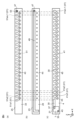
- FIG. 1 is a perspective view of an RFID module according to a first embodiment; A perspective view of an RFID module with the resin layer removed. An exploded perspective view of the substrate disassembled from the coil assembly. A side view of the RFID module with the board removed, viewed in the longitudinal direction A side view of the coil conductor and the substrate viewed in the longitudinal direction. A plan view showing the wiring patterns on each base layer of the substrate.
- FIG. 13 is a perspective view of an RFID module from which a resin layer has been removed according to a modification of the first embodiment; Plan view of resin block FIG. 13 is a perspective view of an RFID module with a resin layer removed according to a second embodiment; FIG.
- FIG. 13 is a perspective view of an RFID module with a resin layer removed according to a third embodiment; 11 is a plan view showing wiring patterns on each main surface of a substrate according to a third embodiment;
- FIG. 13 is a perspective view of an RFID module according to a fourth embodiment; FIG. 13 is a perspective view of an RFID module according to a modification of the fourth embodiment;
- Fig. 1 is an overall perspective view of the RFID module 1 according to the first embodiment.
- Fig. 2 is a perspective view of the RFID module 1 with the resin layer 9 removed.
- Fig. 3 is an exploded perspective view of the coil assembly 6 and the substrate 3 disassembled.
- the X-Y-Z coordinate system is used to facilitate understanding of the invention, but does not limit the invention.
- the X-axis direction indicates the longitudinal direction of the RFID module 1
- the Y-axis direction indicates the depth direction
- the Z-axis direction indicates the thickness direction.
- the X, Y, and Z directions are mutually orthogonal.
- the positive direction of the Z axis is the upward direction
- the negative direction of the Z axis is the downward direction.
- the RFID module 1 of the embodiment includes a substrate 3, a coil assembly 6 connected to a first main surface 4 and a second main surface 5 of the substrate 3, an RFIC chip 7 disposed on the first main surface 4 of the substrate 3, and a resin layer 9 that seals the substrate 3, the coil assembly 6, and the RFIC chip 7.
- the substrate 3 is a double-sided substrate, with the first main surface 4 and the second main surface 5 of the substrate 3 facing each other.
- the substrate 3 is insulating, and is, for example, a glass epoxy substrate or a ceramic substrate.
- the RFIC chip 7 not only outputs information (e.g., ID information and security information) that is pre-stored within the chip, but also includes chips that have built-in sensors for measuring environmental information (e.g., temperature, humidity, pressure) and have the function of outputting the acquired information together with the pre-stored information.
- the resin layer 9 is a molding material that seals the substrate 3, the RFIC chip 7, and the coil conductor 19.
- the resin layer 9 is formed of a general sealing resin such as an epoxy resin.
- the coil assembly 6 includes a plurality of annular electrodes 11.
- the annular electrodes 11 are metallic conductors, and are manufactured, for example, by punching a metal plate. See FIG. 4.
- FIG. 4 is a side view of the RFID module 1 viewed along the longitudinal direction. Note that the substrate 3 is omitted in FIG. 4 for ease of understanding.
- the annular electrode 11 has a first end 13, which is one end, a second end 15, which is the other end, and a gap 17 between the first end 13 and the second end 15.
- the annular electrode 11 has, for example, a shape with a portion of a ring shape missing, and extends continuously from the first end 13 to the second end 15.
- the distance Wa of the gap 17 from the first end 13 to the second end 15 is smaller than the opening diameter Ra of the annular electrode 11, for example, smaller than 1/8 of the opening diameter Ra.
- the annular electrodes 11 are arranged so that the gaps 17 of the annular electrodes 11 are aligned in a straight line. Therefore, as shown in FIG. 5, the substrate 3 can be arranged in the gaps 17 of the annular electrodes 11.
- the first end 13 of the annular electrode 11 is closer to the first main surface 4 than the second main surface 5 of the substrate 3, and the second end 15 of the annular electrode 11 is closer to the second main surface 5 than the first main surface 4 of the substrate 3.
- the substrate 3 is inserted vertically into the gap 17 and is sandwiched between the first end 13 and the second end 15 of the annular electrode 11.
- each annular electrode 11 is connected to the first main surface 4 of the substrate 3, and the second end 15 is connected to the second main surface 5 of the substrate 3. At least a portion of the substrate 3 is arranged inside the inner circumference 12b of the annular electrode 11.
- Each of the multiple annular electrodes 11 of the coil assembly 6 is connected to a conductor pattern arranged on the substrate 3 to form a single coil conductor 19, which functions as an antenna.
- the communication frequency band in the RFID module 1 of the embodiment is, for example, the UHF band from 860 MHz to 960 MHz.
- the number and dimensions of the annular electrodes 11 may be changed according to the communication characteristics.
- Figure 6 is a plan view showing the wiring patterns on each base layer of the substrate 3.
- Figure 6(a) is a perspective plan view of the substrate 3 seen from the first main surface side, showing the conductor pattern on the second main surface 5 of the substrate 3.
- Figure 6(b) is a perspective plan view of the substrate 3 seen from the first main surface side, showing the conductor pattern on the third main surface.
- Figure 6(c) is a perspective plan view of the substrate 3 seen from the first main surface side, showing the conductor pattern on the third main surface.
- the dashed line in Figure 6 indicates the connection by the ring-shaped electrode 11, and the dashed double-dashed line indicates the through-hole connection.
- the substrate 3 is a laminated substrate, and has a first substrate layer 21, a second substrate layer 23, and a third substrate layer 25.
- the third substrate layer 25 is used as the bottom substrate
- the second substrate layer 23 is laminated on the third substrate layer 25
- the first substrate layer 21 is further laminated on the second substrate layer 23.
- the first substrate layer 21 to the third substrate layer 25 are each insulating, and are, for example, a glass epoxy substrate or a ceramic substrate.
- the outer principal surface of the first substrate layer 21 is the first principal surface 4 of the substrate 3.
- the inner principal surface of the first substrate layer 21 is in contact with the principal surface 29 of the second substrate layer 23 on the RFIC chip 7 side.
- the principal surface of the second substrate layer 23 opposite the principal surface 29 is in contact with the inner principal surface 33 of the third substrate layer 25.
- the outer principal surface, which is the bottom surface of the third substrate layer 25, is the second principal surface 5 of the substrate 3.
- the RFIC chip 7 has a first terminal 35 and a second terminal 37, which are input/output terminals.
- a first conductor pattern 39, a plurality of second conductor patterns 41, and interlayer connection conductors 43 and 45 that penetrate the inside of the substrate 3 are arranged on the first main surface 4 of the first base layer 21.
- the first conductor pattern 39 is a pattern for electrically connecting the RFIC chip 7 and the annular electrode 11.
- the second conductor pattern 41 is part of a pattern for electrically connecting the two annular electrodes 11.
- the first end 13 of the annular electrode 11 is connected to one end (upper end) of the second conductor pattern 41 via a solder electrode.
- interlayer connection conductors 45 and 47 that penetrate the inside of the substrate 3 and a third conductor pattern 49 that corresponds to the first pattern are arranged on the main surface 29 of the second base layer 23.
- the interlayer connection conductor 47 and the third conductor pattern 49 are part of a pattern for connecting the annular electrode 11 that is the farthest from the RFIC chip 7 to the RFIC chip 7.
- a plurality of fourth conductor patterns 51, a fifth conductor pattern 53, and interlayer connection conductors 45 and 47 that penetrate the inside of the substrate 3 are arranged on the second principal surface 5 that faces the principal surface 33 of the second base layer 23.
- the fourth conductor pattern 51 is part of a pattern for electrically connecting the two annular electrodes 11.
- one end of the first conductor pattern 39 is electrically connected to the second terminal 37 of the RFIC chip 7 via solder, and the other end of the first conductor pattern 39 is electrically connected to the first end 13 of the annular electrode 11 closest to the RFIC chip 7 via solder.
- the number of annular electrodes 11 in the coil assembly 6 is N.
- N is an integer equal to or greater than 2.
- the N annular electrodes 11 are arranged on one side, for example, as shown in FIG. 3, from the RFIC chip 7 side as annular electrode 11a1, annular electrode 11a2, ..., annular electrode 11an.
- N-1 second conductor patterns 41 are arranged on the first main surface 4 of the first base layer 21, and from the RFIC chip 7 side as second conductor pattern 41a1, second conductor pattern 41a2, ..., second conductor pattern 41an-1.
- N-1 fourth conductor patterns 51 are arranged on the second main surface 5 of the third base layer 25, and from the RFIC chip 7 side as fourth conductor pattern 51a1, fourth conductor pattern 51a2, ..., fourth conductor pattern 51an-1.
- the interlayer connection conductor 43 is a conductive via that connects the first terminal 35 of the RFIC chip 7 on the first substrate layer 21 to the third conductor pattern 49 on the second substrate layer 23.
- the interlayer connection conductor 45 is a conductive via that connects the second conductor pattern 41 on the first substrate layer 21 to the fourth conductor pattern 51 on the third substrate layer 25.
- the interlayer connection conductor 47 is a conductive via that connects the third conductor pattern 49 on the second substrate layer 23 to the fifth conductor pattern 53 on the third substrate layer 25.
- the interlayer connection conductors 43, 45, and 47 are, for example, conductors formed by solidifying (metallizing) a conductive paste that is filled in a hole provided in the insulating substrate 3, but may also be plated through holes.
- the other end of the first conductor pattern 39 of the first substrate layer 21 is electrically connected to the first end 13 of the annular electrode 11a1 closest to the RFIC chip 7 via solder.
- the second end 15 of the annular electrode 11a1 is electrically connected to one end (upper end) of the fourth conductor pattern 51a1 of the third substrate layer 25 via solder.
- the other end (lower end) of the fourth conductor pattern 51a1 of the third substrate layer 25 is electrically connected to the other end (lower end) of the second conductor pattern 41a1 of the first substrate layer 21 via the interlayer connection conductor 45.
- the second conductor pattern 41a1 of the first substrate layer 21 and the first end 13 of the annular electrode 11a2 are electrically connected via solder.
- the second end 15 of the annular electrode 11a2 is electrically connected via solder to one end (upper end) of the fourth conductor pattern 51a2 of the third substrate layer 25.
- the other end (lower end) of the fourth conductor pattern 51a2 of the third substrate layer 25 and the other end (lower end) of the second conductor pattern 41a2 of the first substrate layer 21 are electrically connected via the interlayer connection conductor 45.
- the annular electrodes 11 are electrically connected in sequence in the X-axis direction.
- the coil conductor 19 includes the annular electrode 11, the fourth conductor pattern 51, the interlayer connection conductor 43, and the fifth conductor pattern 53, and functions as one coil.
- the annular electrodes 11 are electrically connected in sequence, and the second end 15 of the annular electrode 11an-1 is electrically connected to one end (upper end) of the fourth conductor pattern 51an-1 of the third substrate layer 25 via solder.
- the other end (lower end) of the fourth conductor pattern 51an-1 of the third substrate layer 25 is electrically connected to the other end (lower end) of the second conductor pattern 41an-1 of the first substrate layer 21 via an interlayer connection conductor 45.
- One end (upper end) of the second conductor pattern 41an-1 of the first substrate layer 21 is electrically connected to the first end 13 of the annular electrode 11an via solder.
- the second end 15 of the annular electrode 11an is electrically connected to the fifth conductor pattern 53 of the third substrate layer 25 via solder.
- the fifth conductor pattern 53 of the third substrate layer 25 and one end of the third conductor pattern 49 of the second substrate layer 23 are electrically connected via the interlayer connection conductor 47.
- the third conductor pattern 49 extends from one end to the other end in the X-axis direction in the third substrate layer 25, and the other end of the third conductor pattern 49 and the first terminal 35 of the RFIC chip 7 of the first substrate layer 21 are electrically connected via the interlayer connection conductor 43.
- the second terminal 37 of the RFIC chip 7 is electrically connected to the first terminal 35 of the RFIC chip 7 through the coil conductor 19, the interlayer connection conductor 47, the third conductor pattern 49, and the interlayer connection conductor 43. As shown in FIG.
- the inside of the annular electrode 11 refers to the inside of the area enclosed by the outer periphery 12a of the annular electrode 11 and the line connecting the outer periphery 12a side of the first end 13 of the annular electrode 11 and the outer periphery 12a side of the second end 15 of the annular electrode 11.
- An LC parallel resonant circuit is configured within the RFID module 1 and is matched to radio waves of the communication frequency, so when the coil conductor 19 receives radio waves of the communication frequency, a current flows through the RFIC chip 7.
- the first conductor pattern 39, the second conductor pattern 41, the third conductor pattern 49, the fourth conductor pattern 51, and the fifth conductor pattern 53 are each a conductor, for example, copper foil patterned by photolithography.
- the RFID module 1 of the first embodiment includes a substrate 3 having a first main surface 4 and a second main surface 5 facing each other, an RFIC chip 7 arranged on the first main surface 4 of the substrate 3, a coil conductor 19 having a plurality of annular electrodes 11, and a third conductor pattern 49 arranged on the substrate 3 as a first pattern electrically connecting the RFIC chip 7 and the coil conductor 19.
- Each of the plurality of annular electrodes 11 has a first end 13 and a second end 15. A gap 17 exists between the first end 13 and the second end 15, and the gaps 17 of the plurality of annular electrodes 11 are each arranged on a straight line.
- the distance Wa of the gap 17 from the first end 13 to the second end 15 is smaller than the opening diameter Ra of the annular electrode 11.
- the plurality of annular electrodes 11 include annular electrodes 11a1 and annular electrodes 11a2.
- the coil conductor 19 has a fourth conductor pattern 51, an interlayer connection conductor 45, and a second conductor pattern 41 as a second pattern that electrically connects the second end 15 of the annular electrode 11a1 and the first end 13 of the annular electrode 11a2. At least a portion of the third conductor pattern 49 is disposed inside the annular electrode 11.
- the third conductor pattern 49 is disposed inside the annular electrode 11, so the opening diameter of the annular electrode 11, which functions as a coil, can be made larger relative to the external size of the RFID module 1. This allows for a longer communication distance relative to the external size of the RFID module 1, and improves the antenna characteristics.
- at least a portion of the third conductor pattern 49 which electrically connects the RFIC chip 7 and the coil conductor 19, is disposed inside the annular electrode 11, so attenuation of the magnetic field generated from the annular electrode 11 by the third conductor pattern 49 can be reduced.
- the width Wb of the substrate 3 is smaller than the opening diameter Ra of the annular electrode 11.
- the opening diameter Ra of the annular electrode 11 can be made larger than the width Wb of the substrate 3, thereby improving the communication characteristics of the RFID module 1.
- the attenuation of the magnetic field generated from the annular electrode 11 by the third conductor pattern 49 can be significantly reduced, thereby further improving the communication characteristics of the RFID module 1.
- first main surface 4 and the second main surface 5 of the substrate 3 intersect with the direction in which the first end 13 and the second end 15 of the annular electrode 11 face each other.
- the substrate 3 is placed in the gap 17 of the annular electrode 11, so that the opening diameter Ra of the annular electrode 11 can be made larger than the external size of the RFID module 1.
- FIG. 7 is a perspective view of an RFID module 1A with the resin layer 9 removed in a modified example of embodiment 1.
- multiple annular electrodes 11 are integrated with a resin block 61 to maintain the pitch of each annular electrode 11.
- the resin block 61 may solidify only a portion of the annular electrodes 11, or may solidify most or all of the annular electrodes 11 while maintaining the gaps 17 between each of the multiple annular electrodes 11.
- the resin block 61 can protect the annular electrodes 11.
- the resin block 61 may be formed by molding the annular electrodes 11 arranged at a predetermined pitch, or the annular electrodes 11 may be fitted into a flexible resin block 61A as shown in FIG. 8.
- the resin block 61A has holes 63 arranged at a predetermined pitch into which the annular electrodes 11A are inserted.
- the holes 63 have notches 65 formed therein that connect to the outer periphery of the resin block 61A.
- the resin block 61A may also be provided with a recess 66 that supports the lower end of the substrate 3, thereby improving the positioning accuracy of the substrate 3.
- Fig. 9 is a perspective view showing an outline of an RFID module 1B according to the second embodiment.
- the annular electrode 11B of the coil conductor 19B of the RFID module 1B in the second embodiment has a rectangular or polygonal shape.
- the configuration of the RFID module 1B in the second embodiment is the same as that of the RFID module 1 in the first embodiment, and a description of the common configuration will be omitted.
- the ring-shaped electrode 11B of the coil conductor 19B shown in FIG. 9 has a substantially octagonal shape, with a gap 17 on one side of the octagon.
- the ring-shaped electrode 11B may be substantially hexagonal, or may be substantially polygonal with 10 or more sides.
- an RFID module 1C which is a modified example of embodiment 2, will be described.
- the first end 13C and the second end 15C may each protrude outwardly of the opening diameter along the substrate 3.
- the mounting area with the substrate 3 can be increased, and the mounting strength can be improved.
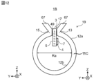
- annular electrode 11C can be manufactured by the following method. As shown in FIG. 11, an annular electrode 11C is formed having protrusions 67 protruding outward from the first end 13C and the second end 15C of the annular electrode 11B with an opening diameter Ra. A plurality of annular electrodes 11C may be integrated by a resin block 61.
- the protrusions 67 can be opened with a tool to insert the substrate 3 into the widened gap 17, reducing the risk of the solder paste applied to the second conductor pattern 41 and the fourth conductor pattern 51 of the substrate 3 coming into contact with other parts of the substrate 3 and flowing.
- the protrusions 67 can be grasped to transport the coil conductor 19C, so that the annular electrode 11C can be transported without being damaged.
- the protruding portion 67 can be cut to form an annular electrode 11C having a first end 13C and a second end 15C that protrude outward as shown in FIG. 10.
- the direction in which the protrusion 67 extends is not limited to a direction parallel to the first main surface 4 and the second main surface 5 of the substrate 3. As shown in FIG. 12, the direction in which the protrusion 67 extends may be a direction intersecting the first main surface 4 and the second main surface 5 of the substrate 3. In this case, the connection end faces of the first end 13 and the second end 15 of the annular electrode 11C to the substrate 3 are inclined with respect to the first main surface 4 and the second main surface 5 of the substrate 3. This makes it possible to increase the attachment area between the first end 13 and the second end 15 of the annular electrode 11C and the substrate 3, and to improve the attachment strength between the annular electrode 11C and the substrate 3.
- FIG. 13 is a perspective view of an RFID module with the resin layer removed according to embodiment 3.
- Fig. 14 is a plan view showing wiring patterns on each main surface of a substrate 3 according to embodiment 3.
- Fig. 14(a) is a plan view of the substrate 3 viewed from the first main surface 4 side, showing the conductor pattern on the first main surface 4 of the substrate 3.
- Fig. 14(b) is a perspective plan view of the substrate 3 viewed from the first main surface 4 side, showing the conductor pattern on the second main surface 5.
- the substrate 3 of the RFID module 1 in embodiment 1 is positioned so as to fit into the gap 17 of the annular electrode 11, whereas the substrate 3 of the RFID module 1D in embodiment 3 is entirely positioned inside the gap 17, i.e., inside the annular electrode 11D.
- the configuration of the RFID module 1D in embodiment 3 is the same as that of the RFID module 1 in embodiment 1, and a description of the common configuration will be omitted.
- An RFIC chip 7 is disposed on the second main surface 5 of the substrate 3D.
- a second terminal 37 of the RFIC chip 7 is electrically connected to a first conductor pattern 39D disposed on the first main surface 4 of the substrate 3D via an interlayer connection conductor.
- the first conductor pattern 39D is also electrically connected to the second end 15 of the annular electrode 11Da1.
- a second conductor pattern 41D electrically connecting the first end 13 of the annular electrode 11Dak and the second end 15 of the adjacent annular electrode 11Dak+1 is arranged on the first main surface 4 of the substrate 3D.
- k is an integer between 1 and N-1.
- the first end 13 and the second end 15 of the annular electrode 11D are attached to the first main surface 4 of the substrate 3D.
- the first end 13 of the annular electrode 11Da1 is electrically connected to one end of the second conductor pattern 41Da1 via solder.
- the other end of the second conductor pattern 41Da1 is electrically connected to the second end 15 of the annular electrode 11Da2 via solder.
- the multiple annular electrodes 11D are electrically connected in sequence via the second conductor pattern 41D, and the second end 15 of the annular electrode 11Dn is electrically connected to one end of the second conductor pattern 41Dan-1 via solder.
- the first end 13 of the annular electrode 11Dn is electrically connected to the fifth conductor pattern 53D via solder.
- the fifth conductor pattern 53D is electrically connected to one end of the third conductor pattern 49D by an interlayer connection conductor.
- the other end of the third conductor pattern 49D is electrically connected to the first terminal 35 of the RFIC chip 7.
- the substrate 3D is entirely disposed inside the annular electrode 11D, so that the substrate 3D is protected from impacts and the like.
- annular electrode 11D of the RFID module 1D in the third embodiment is formed by punching a metal plate
- the annular electrode 11E of the RFID module 1E in the fourth embodiment is formed by rolling a linearly formed pattern electrode on the flexible substrate 71.
- the configuration of the RFID module 1D in the third embodiment and the RFID module 1E in the fourth embodiment is the same, and a description of the common configuration will be omitted.
- substrate 3D and flexible substrate 71 can be attached using a reflow furnace.
- a pattern electrode formed on flexible substrate 71 as annular electrode 11E, costs can be significantly reduced.
- annular electrode 11E can be protected and resin layer 9 can be omitted.
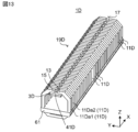
- FIG. 16 is a perspective view of an RFID module 1F according to a modified example of embodiment 4.
- the RFID module 1F further includes a core material 73 in addition to the RFID module 1E of embodiment 4.
- the core material 73 is, for example, a resin material.
- the core material 73 has a generally cylindrical shape, and the flexible substrate 71 is wrapped around and fixed to the core material 73, thereby increasing the strength of the RFID module 1F.
- the substrate 3D may be attached to the core material 73, or may be formed within the core material 73.
- the RFID module includes a substrate having a first main surface and a second main surface facing each other, an RFIC chip disposed on the first main surface of the substrate, a coil conductor having a plurality of annular electrodes, and a first pattern disposed on the substrate and electrically connecting the RFIC chip and the coil conductor.
- Each of the plurality of annular electrodes has a first end and a second end, and a gap exists between the first end and the second end.
- the gaps between the plurality of annular electrodes are disposed on a straight line, and the distance of the gap from the first end to the second end is smaller than the opening diameter of the annular electrode.
- the plurality of annular electrodes include a first annular electrode and a second annular electrode, and the coil conductor has a second pattern electrically connecting the second end of the first annular electrode and the first end of the second annular electrode. At least a part of the first pattern is disposed inside the annular electrodes.
- the first pattern is disposed inside the annular electrode, so the opening diameter of the annular electrode that functions as a coil can be made larger relative to the external size of the RFID module. This makes it possible to increase the communication distance relative to the external size of the RFID module.
- the first pattern is disposed inside the annular electrode, it is possible to reduce attenuation of the magnetic field generated from the annular electrode by the first pattern of the RFID module.
- the width of the substrate is smaller than the opening diameter of the annular electrode.
- the first pattern connects the RFIC chip to the annular electrode that is positioned farthest from the RFIC chip.
- the entire first pattern is disposed inside the annular electrode.
- the first and second main surfaces of the substrate intersect with the direction in which the first and second ends of the annular electrode face each other.
- the first end of the annular electrode is closer to the first main surface of the substrate than the second main surface of the substrate, and the second end of the annular electrode is closer to the second main surface of the substrate than the first main surface of the substrate.
- the first and second ends of the annular electrode are inclined with respect to the first and second main surfaces of the substrate, respectively.
- the multiple annular electrodes are pattern electrodes arranged on a flexible substrate.
- the second pattern is disposed on the first main surface or the second main surface of the substrate, and the first end and the second end of the annular electrode are disposed on either the first main surface or the second main surface of the substrate.
- a resin core material is provided, and a flexible substrate is wound around the core material.
Landscapes
- Engineering & Computer Science (AREA)
- Computer Hardware Design (AREA)
- Microelectronics & Electronic Packaging (AREA)
- Physics & Mathematics (AREA)
- General Physics & Mathematics (AREA)
- Theoretical Computer Science (AREA)
- Coils Or Transformers For Communication (AREA)
Priority Applications (1)
| Application Number | Priority Date | Filing Date | Title |
|---|---|---|---|
| JP2025556216A JPWO2025100050A1 (https=) | 2023-11-06 | 2024-08-28 |
Applications Claiming Priority (2)
| Application Number | Priority Date | Filing Date | Title |
|---|---|---|---|
| JP2023189507 | 2023-11-06 | ||
| JP2023-189507 | 2023-11-06 |
Publications (1)
| Publication Number | Publication Date |
|---|---|
| WO2025100050A1 true WO2025100050A1 (ja) | 2025-05-15 |
Family
ID=95695544
Family Applications (1)
| Application Number | Title | Priority Date | Filing Date |
|---|---|---|---|
| PCT/JP2024/030672 Pending WO2025100050A1 (ja) | 2023-11-06 | 2024-08-28 | Rfidモジュール |
Country Status (2)
| Country | Link |
|---|---|
| JP (1) | JPWO2025100050A1 (https=) |
| WO (1) | WO2025100050A1 (https=) |
Cited By (1)
| Publication number | Priority date | Publication date | Assignee | Title |
|---|---|---|---|---|
| WO2026053597A1 (ja) * | 2024-09-05 | 2026-03-12 | 株式会社村田製作所 | Rfidモジュール及び無線通信デバイス |
Citations (2)
| Publication number | Priority date | Publication date | Assignee | Title |
|---|---|---|---|---|
| WO2016098379A1 (ja) * | 2014-12-19 | 2016-06-23 | 株式会社村田製作所 | 無線icデバイス、樹脂成型体およびその製造方法 |
| WO2018235714A1 (ja) * | 2017-06-19 | 2018-12-27 | 株式会社村田製作所 | コイル素体集合体およびコイルモジュールとその製造方法 |
-
2024
- 2024-08-28 WO PCT/JP2024/030672 patent/WO2025100050A1/ja active Pending
- 2024-08-28 JP JP2025556216A patent/JPWO2025100050A1/ja active Pending
Patent Citations (2)
| Publication number | Priority date | Publication date | Assignee | Title |
|---|---|---|---|---|
| WO2016098379A1 (ja) * | 2014-12-19 | 2016-06-23 | 株式会社村田製作所 | 無線icデバイス、樹脂成型体およびその製造方法 |
| WO2018235714A1 (ja) * | 2017-06-19 | 2018-12-27 | 株式会社村田製作所 | コイル素体集合体およびコイルモジュールとその製造方法 |
Cited By (1)
| Publication number | Priority date | Publication date | Assignee | Title |
|---|---|---|---|---|
| WO2026053597A1 (ja) * | 2024-09-05 | 2026-03-12 | 株式会社村田製作所 | Rfidモジュール及び無線通信デバイス |
Also Published As
| Publication number | Publication date |
|---|---|
| JPWO2025100050A1 (https=) | 2025-05-15 |
Similar Documents
| Publication | Publication Date | Title |
|---|---|---|
| CN106847771B (zh) | 具有天线的半导体封装及其制作方法 | |
| US9748652B2 (en) | Manufacturing method for a magnetic material core-embedded resin multilayer board | |
| US9697946B2 (en) | Electronic component | |
| JP6008069B1 (ja) | 無線icデバイス、それを備えた樹脂成型体、それを備えた通信端末装置、及びその製造方法 | |
| US20050052268A1 (en) | Embedded toroidal inductors | |
| JP6535450B2 (ja) | 電子部品 | |
| GB2461443A (en) | Magnetic field coupling type antenna, magnetic field coupling type antenna module, magnetic field coupling type antenna device,and their manufacturing methods | |
| CN106463833B (zh) | 无线ic设备、树脂成型体及线圈天线的制造方法 | |
| JP6380648B2 (ja) | コイルデバイスおよび電子デバイス | |
| CN106233310A (zh) | 无线ic器件、树脂成型体及其制造方法 | |
| KR20160108934A (ko) | 코일 부품 및 그 실장 기판 | |
| US11949144B2 (en) | Structure for mounting a transmission line substrate having interlayer connection conductors to another substrate by a conductive bonding material | |
| CN108604491A (zh) | 电感器部件及其制造方法 | |
| WO2025100050A1 (ja) | Rfidモジュール | |
| EP3561955B1 (en) | Antenna substrate | |
| KR20160092265A (ko) | 코일 부품 및 그 실장 기판 | |
| KR102029491B1 (ko) | 코일 부품 및 그 실장 기판 | |
| US10096901B2 (en) | Coil module | |
| EP2933878B1 (en) | Antenna device | |
| US9076801B2 (en) | Module IC package structure | |
| KR100519815B1 (ko) | 칩 인덕터 | |
| US20070178729A1 (en) | Electronic circuit module and method for fabrication thereof | |
| US10506717B2 (en) | Inductor component and method of manufacturing inductor component | |
| WO2024048715A1 (ja) | Rfidモジュール | |
| JP7733359B2 (ja) | Rfidモジュール |
Legal Events
| Date | Code | Title | Description |
|---|---|---|---|
| 121 | Ep: the epo has been informed by wipo that ep was designated in this application |
Ref document number: 24888352 Country of ref document: EP Kind code of ref document: A1 |
|
| ENP | Entry into the national phase |
Ref document number: 2025556216 Country of ref document: JP Kind code of ref document: A |
|
| WWE | Wipo information: entry into national phase |
Ref document number: 2025556216 Country of ref document: JP |