WO2025069736A1 - プラズマ処理装置及び基板処理システム - Google Patents
プラズマ処理装置及び基板処理システム Download PDFInfo
- Publication number
- WO2025069736A1 WO2025069736A1 PCT/JP2024/028533 JP2024028533W WO2025069736A1 WO 2025069736 A1 WO2025069736 A1 WO 2025069736A1 JP 2024028533 W JP2024028533 W JP 2024028533W WO 2025069736 A1 WO2025069736 A1 WO 2025069736A1
- Authority
- WO
- WIPO (PCT)
- Prior art keywords
- ring
- edge ring
- plasma processing
- processing apparatus
- substrate
- Prior art date
- Legal status (The legal status is an assumption and is not a legal conclusion. Google has not performed a legal analysis and makes no representation as to the accuracy of the status listed.)
- Ceased
Links
Images







Classifications
-
- H—ELECTRICITY
- H10—SEMICONDUCTOR DEVICES; ELECTRIC SOLID-STATE DEVICES NOT OTHERWISE PROVIDED FOR
- H10P—GENERIC PROCESSES OR APPARATUS FOR THE MANUFACTURE OR TREATMENT OF DEVICES COVERED BY CLASS H10
- H10P72/00—Handling or holding of wafers, substrates or devices during manufacture or treatment thereof
- H10P72/04—Apparatus for manufacture or treatment
- H10P72/0402—Apparatus for fluid treatment
- H10P72/0418—Apparatus for fluid treatment for etching
- H10P72/0421—Apparatus for fluid treatment for etching for drying etching
-
- C—CHEMISTRY; METALLURGY
- C23—COATING METALLIC MATERIAL; COATING MATERIAL WITH METALLIC MATERIAL; CHEMICAL SURFACE TREATMENT; DIFFUSION TREATMENT OF METALLIC MATERIAL; COATING BY VACUUM EVAPORATION, BY SPUTTERING, BY ION IMPLANTATION OR BY CHEMICAL VAPOUR DEPOSITION, IN GENERAL; INHIBITING CORROSION OF METALLIC MATERIAL OR INCRUSTATION IN GENERAL
- C23C—COATING METALLIC MATERIAL; COATING MATERIAL WITH METALLIC MATERIAL; SURFACE TREATMENT OF METALLIC MATERIAL BY DIFFUSION INTO THE SURFACE, BY CHEMICAL CONVERSION OR SUBSTITUTION; COATING BY VACUUM EVAPORATION, BY SPUTTERING, BY ION IMPLANTATION OR BY CHEMICAL VAPOUR DEPOSITION, IN GENERAL
- C23C16/00—Chemical coating by decomposition of gaseous compounds, without leaving reaction products of surface material in the coating, i.e. chemical vapour deposition [CVD] processes
- C23C16/44—Chemical coating by decomposition of gaseous compounds, without leaving reaction products of surface material in the coating, i.e. chemical vapour deposition [CVD] processes characterised by the method of coating
- C23C16/46—Chemical coating by decomposition of gaseous compounds, without leaving reaction products of surface material in the coating, i.e. chemical vapour deposition [CVD] processes characterised by the method of coating characterised by the method used for heating the substrate
-
- H—ELECTRICITY
- H01—ELECTRIC ELEMENTS
- H01J—ELECTRIC DISCHARGE TUBES OR DISCHARGE LAMPS
- H01J37/00—Discharge tubes with provision for introducing objects or material to be exposed to the discharge, e.g. for the purpose of examination or processing thereof
- H01J37/32—Gas-filled discharge tubes
- H01J37/32009—Arrangements for generation of plasma specially adapted for examination or treatment of objects, e.g. plasma sources
- H01J37/32082—Radio frequency generated discharge
- H01J37/321—Radio frequency generated discharge the radio frequency energy being inductively coupled to the plasma
-
- H—ELECTRICITY
- H01—ELECTRIC ELEMENTS
- H01J—ELECTRIC DISCHARGE TUBES OR DISCHARGE LAMPS
- H01J37/00—Discharge tubes with provision for introducing objects or material to be exposed to the discharge, e.g. for the purpose of examination or processing thereof
- H01J37/32—Gas-filled discharge tubes
- H01J37/32009—Arrangements for generation of plasma specially adapted for examination or treatment of objects, e.g. plasma sources
- H01J37/32082—Radio frequency generated discharge
- H01J37/32174—Circuits specially adapted for controlling the RF discharge
-
- H—ELECTRICITY
- H01—ELECTRIC ELEMENTS
- H01J—ELECTRIC DISCHARGE TUBES OR DISCHARGE LAMPS
- H01J37/00—Discharge tubes with provision for introducing objects or material to be exposed to the discharge, e.g. for the purpose of examination or processing thereof
- H01J37/32—Gas-filled discharge tubes
- H01J37/32431—Constructional details of the reactor
- H01J37/32623—Mechanical discharge control means
- H01J37/32642—Focus rings
-
- H—ELECTRICITY
- H01—ELECTRIC ELEMENTS
- H01J—ELECTRIC DISCHARGE TUBES OR DISCHARGE LAMPS
- H01J37/00—Discharge tubes with provision for introducing objects or material to be exposed to the discharge, e.g. for the purpose of examination or processing thereof
- H01J37/32—Gas-filled discharge tubes
- H01J37/32431—Constructional details of the reactor
- H01J37/32697—Electrostatic control
-
- H—ELECTRICITY
- H01—ELECTRIC ELEMENTS
- H01J—ELECTRIC DISCHARGE TUBES OR DISCHARGE LAMPS
- H01J37/00—Discharge tubes with provision for introducing objects or material to be exposed to the discharge, e.g. for the purpose of examination or processing thereof
- H01J37/32—Gas-filled discharge tubes
- H01J37/32431—Constructional details of the reactor
- H01J37/32715—Workpiece holder
-
- H—ELECTRICITY
- H01—ELECTRIC ELEMENTS
- H01J—ELECTRIC DISCHARGE TUBES OR DISCHARGE LAMPS
- H01J37/00—Discharge tubes with provision for introducing objects or material to be exposed to the discharge, e.g. for the purpose of examination or processing thereof
- H01J37/32—Gas-filled discharge tubes
- H01J37/32431—Constructional details of the reactor
- H01J37/32798—Further details of plasma apparatus not provided for in groups H01J37/3244 - H01J37/32788; special provisions for cleaning or maintenance of the apparatus
- H01J37/32807—Construction (includes replacing parts of the apparatus)
-
- H—ELECTRICITY
- H01—ELECTRIC ELEMENTS
- H01J—ELECTRIC DISCHARGE TUBES OR DISCHARGE LAMPS
- H01J37/00—Discharge tubes with provision for introducing objects or material to be exposed to the discharge, e.g. for the purpose of examination or processing thereof
- H01J37/32—Gas-filled discharge tubes
- H01J37/32431—Constructional details of the reactor
- H01J37/32798—Further details of plasma apparatus not provided for in groups H01J37/3244 - H01J37/32788; special provisions for cleaning or maintenance of the apparatus
- H01J37/32889—Connection or combination with other apparatus
-
- H—ELECTRICITY
- H01—ELECTRIC ELEMENTS
- H01J—ELECTRIC DISCHARGE TUBES OR DISCHARGE LAMPS
- H01J37/00—Discharge tubes with provision for introducing objects or material to be exposed to the discharge, e.g. for the purpose of examination or processing thereof
- H01J37/32—Gas-filled discharge tubes
- H01J37/32917—Plasma diagnostics
- H01J37/3299—Feedback systems
-
- H—ELECTRICITY
- H05—ELECTRIC TECHNIQUES NOT OTHERWISE PROVIDED FOR
- H05H—PLASMA TECHNIQUE; PRODUCTION OF ACCELERATED ELECTRICALLY-CHARGED PARTICLES OR OF NEUTRONS; PRODUCTION OR ACCELERATION OF NEUTRAL MOLECULAR OR ATOMIC BEAMS
- H05H1/00—Generating plasma; Handling plasma
- H05H1/24—Generating plasma
- H05H1/46—Generating plasma using applied electromagnetic fields, e.g. high frequency or microwave energy
-
- H—ELECTRICITY
- H10—SEMICONDUCTOR DEVICES; ELECTRIC SOLID-STATE DEVICES NOT OTHERWISE PROVIDED FOR
- H10P—GENERIC PROCESSES OR APPARATUS FOR THE MANUFACTURE OR TREATMENT OF DEVICES COVERED BY CLASS H10
- H10P50/00—Etching of wafers, substrates or parts of devices
- H10P50/20—Dry etching; Plasma etching; Reactive-ion etching
- H10P50/24—Dry etching; Plasma etching; Reactive-ion etching of semiconductor materials
- H10P50/242—Dry etching; Plasma etching; Reactive-ion etching of semiconductor materials of Group IV materials
-
- H—ELECTRICITY
- H10—SEMICONDUCTOR DEVICES; ELECTRIC SOLID-STATE DEVICES NOT OTHERWISE PROVIDED FOR
- H10P—GENERIC PROCESSES OR APPARATUS FOR THE MANUFACTURE OR TREATMENT OF DEVICES COVERED BY CLASS H10
- H10P72/00—Handling or holding of wafers, substrates or devices during manufacture or treatment thereof
- H10P72/04—Apparatus for manufacture or treatment
- H10P72/0451—Apparatus for manufacturing or treating in a plurality of work-stations
- H10P72/0464—Apparatus for manufacturing or treating in a plurality of work-stations characterised by the construction of the transfer chamber
-
- H—ELECTRICITY
- H10—SEMICONDUCTOR DEVICES; ELECTRIC SOLID-STATE DEVICES NOT OTHERWISE PROVIDED FOR
- H10P—GENERIC PROCESSES OR APPARATUS FOR THE MANUFACTURE OR TREATMENT OF DEVICES COVERED BY CLASS H10
- H10P72/00—Handling or holding of wafers, substrates or devices during manufacture or treatment thereof
- H10P72/06—Apparatus for monitoring, sorting, marking, testing or measuring
- H10P72/0604—Process monitoring, e.g. flow or thickness monitoring
-
- H—ELECTRICITY
- H10—SEMICONDUCTOR DEVICES; ELECTRIC SOLID-STATE DEVICES NOT OTHERWISE PROVIDED FOR
- H10P—GENERIC PROCESSES OR APPARATUS FOR THE MANUFACTURE OR TREATMENT OF DEVICES COVERED BY CLASS H10
- H10P72/00—Handling or holding of wafers, substrates or devices during manufacture or treatment thereof
- H10P72/70—Handling or holding of wafers, substrates or devices during manufacture or treatment thereof for supporting or gripping
- H10P72/72—Handling or holding of wafers, substrates or devices during manufacture or treatment thereof for supporting or gripping using electrostatic chucks
- H10P72/722—Details of electrostatic chucks
-
- H—ELECTRICITY
- H10—SEMICONDUCTOR DEVICES; ELECTRIC SOLID-STATE DEVICES NOT OTHERWISE PROVIDED FOR
- H10P—GENERIC PROCESSES OR APPARATUS FOR THE MANUFACTURE OR TREATMENT OF DEVICES COVERED BY CLASS H10
- H10P72/00—Handling or holding of wafers, substrates or devices during manufacture or treatment thereof
- H10P72/70—Handling or holding of wafers, substrates or devices during manufacture or treatment thereof for supporting or gripping
- H10P72/76—Handling or holding of wafers, substrates or devices during manufacture or treatment thereof for supporting or gripping using mechanical means, e.g. clamps or pinches
- H10P72/7604—Handling or holding of wafers, substrates or devices during manufacture or treatment thereof for supporting or gripping using mechanical means, e.g. clamps or pinches the wafers being placed on a susceptor, stage or support
- H10P72/7611—Handling or holding of wafers, substrates or devices during manufacture or treatment thereof for supporting or gripping using mechanical means, e.g. clamps or pinches the wafers being placed on a susceptor, stage or support characterised by edge profile or support profile
-
- H—ELECTRICITY
- H10—SEMICONDUCTOR DEVICES; ELECTRIC SOLID-STATE DEVICES NOT OTHERWISE PROVIDED FOR
- H10P—GENERIC PROCESSES OR APPARATUS FOR THE MANUFACTURE OR TREATMENT OF DEVICES COVERED BY CLASS H10
- H10P72/00—Handling or holding of wafers, substrates or devices during manufacture or treatment thereof
- H10P72/70—Handling or holding of wafers, substrates or devices during manufacture or treatment thereof for supporting or gripping
- H10P72/76—Handling or holding of wafers, substrates or devices during manufacture or treatment thereof for supporting or gripping using mechanical means, e.g. clamps or pinches
- H10P72/7604—Handling or holding of wafers, substrates or devices during manufacture or treatment thereof for supporting or gripping using mechanical means, e.g. clamps or pinches the wafers being placed on a susceptor, stage or support
- H10P72/7612—Handling or holding of wafers, substrates or devices during manufacture or treatment thereof for supporting or gripping using mechanical means, e.g. clamps or pinches the wafers being placed on a susceptor, stage or support characterised by lifting arrangements, e.g. lift pins
-
- H—ELECTRICITY
- H01—ELECTRIC ELEMENTS
- H01J—ELECTRIC DISCHARGE TUBES OR DISCHARGE LAMPS
- H01J2237/00—Discharge tubes exposing object to beam, e.g. for analysis treatment, etching, imaging
- H01J2237/32—Processing objects by plasma generation
- H01J2237/33—Processing objects by plasma generation characterised by the type of processing
- H01J2237/334—Etching
Definitions
- An exemplary embodiment of the present disclosure relates to a plasma processing apparatus and a substrate processing system.
- a plasma processing apparatus is used for plasma processing of a substrate.
- the plasma processing apparatus includes a chamber and a substrate support.
- the substrate support is disposed within the chamber.
- the substrate support includes a base and an electrostatic chuck.
- a bias power supply is connected to the base, which generates an electric bias for attracting ions from the plasma to the substrate.
- the electrostatic chuck is configured to support the substrate and an edge ring surrounding the substrate.
- Patent Document 1 discloses a plasma processing apparatus configured to move the edge ring up and down.
- a plasma processing apparatus in one exemplary embodiment, includes a chamber, a substrate support, an edge ring, a lift mechanism, a plasma generation unit, and a bias power supply.
- the substrate support is disposed in the chamber.
- the edge ring is conductive and disposed to surround the substrate on the substrate support.
- the lift mechanism is configured to move the edge ring up and down.
- the plasma generation unit includes a high frequency power supply and is configured to generate plasma in the chamber.
- the bias power supply is configured to generate an electrical bias to attract ions from the plasma to the substrate on the substrate support.
- the substrate support includes a base electrically coupled to the bias power supply and/or the high frequency power supply, and an electrostatic chuck on the base.
- the lift mechanism includes a conductive ring, a rod, an actuator, and a connecting member.
- the conductive ring supports the edge ring placed thereon and is electrically connected to the edge ring.
- the rod extends vertically below the conductive ring.
- the actuator is configured to move the edge ring up and down via the rod and the conductive ring.
- the connecting member provides an electrical connection between the conductive ring and the base. The connection member is configured to maintain the electrical connection in response to movement of the conductive ring.
- FIG. 1 is a diagram for explaining a configuration example of a plasma processing system.
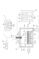
- FIG. 1 is a diagram for explaining a configuration example of an inductively coupled plasma processing apparatus.
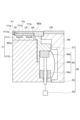
- FIG. 2 illustrates a substrate support and lift mechanism according to an example embodiment.
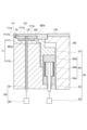
- FIG. 1 illustrates a substrate support and lift mechanism of another exemplary embodiment.
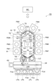
- FIG. 1 illustrates a substrate processing system according to an exemplary embodiment.
- FIG. 13 illustrates a substrate support and lift mechanism according to yet another exemplary embodiment.
- FIG. 13 illustrates a substrate support and lift mechanism according to yet another exemplary embodiment.
- FIG. 13 illustrates a substrate support and lift mechanism according to yet another exemplary embodiment.
- FIG. 13 illustrates a substrate support and lift mechanism according to yet another exemplary embodiment.
- FIG. 13 illustrates a substrate support and lift mechanism according to yet another exemplary embodiment.
- FIG. 13 illustrates a substrate support and lift mechanism according to yet another exemplary embodiment.
- FIG. 13 illustrates a substrate support and lift mechanism according to yet another
- FIG. 13 illustrates a substrate support and lift mechanism according to yet another exemplary embodiment.
- FIG. 13 illustrates a substrate support and lift mechanism according to yet another exemplary embodiment.
- FIG. 13 illustrates a substrate support and lift mechanism according to yet another exemplary embodiment.
- 1 is a flow diagram illustrating a plasma processing method according to an exemplary embodiment.
- FIG. 15(a) is a diagram illustrating an example of an imaging device that can be used with the plasma processing apparatus according to various exemplary embodiments
- FIG. 15(b) is a diagram illustrating an example of a measuring device that can be used with the plasma processing apparatus according to various exemplary embodiments.
- FIG. 4 is a flow diagram illustrating a plasma processing method according to another exemplary embodiment.
- 13 is a flow diagram illustrating a plasma processing method according to yet another exemplary embodiment.
- 1A-1C illustrate example metrology instruments for use with plasma processing apparatus according to various exemplary embodiments.
- FIG. 13 illustrates an edge ring and a conductive ring according to yet another exemplary embodiment.
- FIG. 13 illustrates an edge ring and a conductive ring according to yet another exemplary embodiment.
- FIG. 13 illustrates a substrate support and lift mechanism according to yet another exemplary embodiment.
- 13 is a graph showing experimental results.
- FIG. 2 illustrates a substrate support and lift mechanism according to an example embodiment.
- FIG. 1 is a diagram for explaining an example of the configuration of a plasma processing system.
- the plasma processing system includes a plasma processing device 1 and a control unit 2.
- the plasma processing system is an example of a substrate processing system
- the plasma processing device 1 is an example of a substrate processing device.
- the plasma processing device 1 includes a plasma processing chamber 10, a substrate support unit 11, and a plasma generation unit 12.
- the plasma processing chamber 10 has a plasma processing space.
- the plasma processing chamber 10 also has at least one gas supply port for supplying at least one processing gas to the plasma processing space, and at least one gas exhaust port for exhausting gas from the plasma processing space.
- the gas supply port is connected to a gas supply unit 20 described later, and the gas exhaust port is connected to an exhaust system 40 described later.
- the substrate support unit 11 is disposed in the plasma processing space, and has a substrate support surface for supporting a substrate.
- the plasma generating unit 12 is configured to generate plasma from at least one processing gas supplied into the plasma processing space.
- the plasma formed in the plasma processing space may be capacitively coupled plasma (CCP), inductively coupled plasma (ICP), ECR plasma (Electron-Cyclotron-Resonance Plasma), helicon wave plasma (HWP), or surface wave plasma (SWP), etc.
- various types of plasma generating units may be used, including AC (Alternating Current) plasma generating units and DC (Direct Current) plasma generating units.
- the AC signal (AC power) used in the AC plasma generating unit has a frequency in the range of 100 kHz to 10 GHz.
- AC signals include RF (Radio Frequency) signals and microwave signals.
- the RF signal has a frequency in the range of 100 kHz to 150 MHz.
- the control unit 2 processes computer-executable instructions that cause the plasma processing apparatus 1 to perform the various steps described in this disclosure.
- the control unit 2 may be configured to control each element of the plasma processing apparatus 1 to perform the various steps described herein. In one embodiment, a part or all of the control unit 2 may be included in the plasma processing apparatus 1.
- the control unit 2 may include a processing unit 2a1, a storage unit 2a2, and a communication interface 2a3.
- the control unit 2 is realized, for example, by a computer 2a.
- the processing unit 2a1 may be configured to perform various control operations by reading a program from the storage unit 2a2 and executing the read program. This program may be stored in the storage unit 2a2 in advance, or may be acquired via a medium when necessary.
- the acquired program is stored in the storage unit 2a2 and is read from the storage unit 2a2 by the processing unit 2a1 and executed.
- the medium may be various storage media readable by the computer 2a, or may be a communication line connected to the communication interface 2a3.
- the processing unit 2a1 may be a CPU (Central Processing Unit).
- the memory unit 2a2 may include a RAM (Random Access Memory), a ROM (Read Only Memory), a HDD (Hard Disk Drive), a SSD (Solid State Drive), or a combination of these.
- the communication interface 2a3 may communicate with the plasma processing device 1 via a communication line such as a LAN (Local Area Network).
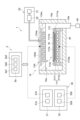
- FIG. 1 is a diagram for explaining an example of the configuration of an inductively coupled plasma processing device.
- the inductively coupled plasma processing apparatus 1 includes a plasma processing chamber 10, a gas supply unit 20, a power supply 30, and an exhaust system 40.
- the plasma processing chamber 10 includes a dielectric window 101.
- the plasma processing apparatus 1 also includes a substrate support unit 11, a gas introduction unit, and an antenna 14.
- the substrate support unit 11 is disposed within the plasma processing chamber 10.
- the antenna 14 is disposed on or above the plasma processing chamber 10 (i.e., on or above the dielectric window 101).
- the plasma processing chamber 10 has a plasma processing space 10s defined by the dielectric window 101, a sidewall 102 of the plasma processing chamber 10, and the substrate support unit 11.
- the plasma processing chamber 10 is grounded.
- the substrate support 11 includes a main body 111 and a ring assembly 112.
- the main body 111 has a central region 111a for supporting the substrate W and an annular region 111b for supporting the ring assembly 112.
- a wafer is an example of a substrate W.
- the annular region 111b of the main body 111 surrounds the central region 111a of the main body 111 in a plan view.
- the substrate W is disposed on the central region 111a of the main body 111
- the ring assembly 112 is disposed on the annular region 111b of the main body 111 so as to surround the substrate W on the central region 111a of the main body 111. Therefore, the central region 111a is also called a substrate support surface for supporting the substrate W, and the annular region 111b is also called a ring support surface for supporting the ring assembly 112.
- the main body 111 includes a base 1110 and an electrostatic chuck 1111.
- the base 1110 includes a conductive member.
- the conductive member of the base 1110 may function as a bias electrode.
- the electrostatic chuck 1111 is disposed on the base 1110.
- the electrostatic chuck 1111 includes a ceramic member 1111a and an electrostatic electrode 1111b disposed within the ceramic member 1111a.
- the ceramic member 1111a has a central region 111a. In one embodiment, the ceramic member 1111a also has an annular region 111b. Note that other members surrounding the electrostatic chuck 1111, such as an annular electrostatic chuck or an annular insulating member, may have the annular region 111b.
- the ring assembly 112 may be disposed on the annular electrostatic chuck or the annular insulating member, or may be disposed on both the electrostatic chuck 1111 and the annular insulating member.
- at least one RF/DC electrode coupled to an RF power source 31 and/or a DC power source 32, which will be described later, may be disposed within the ceramic member 1111a.
- the at least one RF/DC electrode functions as a bias electrode.
- the conductive member of the base 1110 and the at least one RF/DC electrode may function as multiple bias electrodes.
- the electrostatic electrode 1111b may function as a bias electrode.
- the substrate support 11 includes at least one bias electrode.
- the ring assembly 112 includes one or more annular members.
- the one or more annular members include one or more edge rings and at least one cover ring.
- the edge rings are formed of a conductive or insulating material, and the cover rings are formed of an insulating material.
- the substrate support 11 may also include a temperature adjustment module configured to adjust at least one of the electrostatic chuck 1111, the ring assembly 112, and the substrate to a target temperature.
- the temperature adjustment module may include a heater, a heat transfer medium, a flow passage 1110a, or a combination thereof.
- a heat transfer fluid such as brine or a gas flows through the flow passage 1110a.
- the flow passage 1110a is formed in the base 1110, and one or more heaters are disposed in the ceramic member 1111a of the electrostatic chuck 1111.
- the substrate support 11 may also include a heat transfer gas supply configured to supply a heat transfer gas to a gap between the back surface of the substrate W and the central region 111a.
- the gas introduction section is configured to introduce at least one processing gas from the gas supply section 20 into the plasma processing space 10s.
- the gas introduction section includes a center gas injector (CGI) 13.
- the center gas injector 13 is disposed above the substrate support section 11 and attached to a central opening formed in the dielectric window 101.
- the center gas injector 13 has at least one gas supply port 13a, at least one gas flow path 13b, and at least one gas inlet port 13c.
- the processing gas supplied to the gas supply port 13a passes through the gas flow path 13b and is introduced into the plasma processing space 10s from the gas inlet port 13c.
- the gas introduction section may include one or more side gas injectors (SGI) attached to one or more openings formed in the sidewall 102.
- SGI side gas injectors
- the gas supply unit 20 may include at least one gas source 21 and at least one flow controller 22.
- the gas supply unit 20 is configured to supply at least one process gas from a corresponding gas source 21 to the gas inlet via a corresponding flow controller 22.
- Each flow controller 22 may include, for example, a mass flow controller or a pressure-controlled flow controller.
- the gas supply unit 20 may include at least one flow modulation device that modulates or pulses the flow rate of the at least one process gas.
- the power supply 30 includes an RF power supply 31 coupled to the plasma processing chamber 10 via at least one impedance matching circuit.
- the RF power supply 31 is configured to supply at least one RF signal (RF power) to at least one bias electrode and the antenna 14. This causes a plasma to be formed from at least one processing gas supplied to the plasma processing space 10s.
- the RF power supply 31 can function as at least a part of the plasma generating unit 12.
- a bias RF signal to at least one bias electrode, a bias potential is generated on the substrate W, and ions in the formed plasma can be attracted to the substrate W.
- the second RF generating unit 31b is coupled to at least one bias electrode via at least one impedance matching circuit and configured to generate a bias RF signal (bias RF power).
- the frequency of the bias RF signal may be the same as or different from the frequency of the source RF signal.
- the bias RF signal has a lower frequency than the frequency of the source RF signal.
- the bias RF signal has a frequency in the range of 100 kHz to 60 MHz.
- the second RF generating unit 31b may be configured to generate multiple bias RF signals having different frequencies.
- the generated one or more bias RF signals are supplied to at least one bias electrode.
- at least one of the source RF signal and the bias RF signal may be pulsed.
- the power supply 30 may also include a DC power supply 32 coupled to the plasma processing chamber 10.
- the DC power supply 32 includes a bias DC generator 32a.
- the bias DC generator 32a is connected to at least one bias electrode and configured to generate a bias DC signal. The generated bias DC signal is applied to the at least one bias electrode.
- the bias DC signal may be pulsed.
- a sequence of voltage pulses is applied to at least one bias electrode.
- the voltage pulses may have a rectangular, trapezoidal, triangular, or combination of these pulse waveforms.
- a waveform generator for generating a sequence of voltage pulses from the DC signal is connected between the bias DC generator 32a and at least one bias electrode.
- the bias DC generator 32a and the waveform generator constitute a voltage pulse generator.
- the voltage pulses may have a positive polarity or a negative polarity.
- the sequence of voltage pulses may include one or more positive voltage pulses and one or more negative voltage pulses within one period.
- the bias DC generator 32a may be provided in addition to the RF power source 31 or may be provided instead of the second RF generator 31b.
- the antenna 14 includes one or more coils.
- the antenna 14 may include an outer coil and an inner coil arranged coaxially.
- the RF power source 31 may be connected to both the outer coil and the inner coil, or to either the outer coil or the inner coil.
- the same RF generator may be connected to both the outer coil and the inner coil, or separate RF generators may be connected separately to the outer coil and the inner coil.
- the exhaust system 40 may be connected to, for example, a gas exhaust port 10e provided at the bottom of the plasma processing chamber 10.
- the exhaust system 40 may include a pressure regulating valve and a vacuum pump. The pressure in the plasma processing space 10s is adjusted by the pressure regulating valve.
- the vacuum pump may include a turbomolecular pump, a dry pump, or a combination thereof.
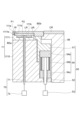
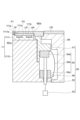
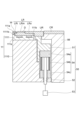
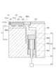
- FIG. 3 is a diagram showing a substrate support and lift mechanism according to one exemplary embodiment.
- the substrate support 11 and lift mechanism 50 shown in FIG. 3 can be employed in the plasma processing apparatus 1.
- the substrate support 11 is configured to support an edge ring UR (upper edge ring).
- the edge ring UR is part of the ring assembly 112.
- the edge ring UR is arranged to surround the substrate W on the substrate support 11.
- the edge ring UR is made of a conductive material such as silicon, silicon carbide, tungsten, etc.
- the substrate support 11 includes a base 1110 and an electrostatic chuck 1111, as described above.
- the base 1110 is or includes a conductive member therein.
- At least one bias power supply such as a second RF generator 31b and/or a bias DC generator 32a, is electrically coupled to the base 1110 (or its conductive member).
- the at least one bias power supply is configured to generate an electrical bias to attract ions from the plasma to the substrate W on the substrate support 11.
- the electrical bias includes a sequence of bias RF signals and/or voltage pulses as described above.
- the electrostatic chuck 1111 is disposed on the base 1110.
- the electrostatic chuck 1111 includes a first portion P1 and a second portion P2.
- the first portion P1 has a substrate support surface (i.e., a central region 111a) as its upper surface.
- the first portion P1 and the substrate support surface have a substantially circular planar shape.
- the central axis of the first portion P1 and the substrate support surface is the central axis of the substrate support portion 11.
- the first portion P1 includes the electrostatic electrode 1111b described above. When a DC voltage is applied to the electrostatic electrode 1111b from a DC power supply, an electrostatic attractive force is generated between the first portion P1 and the substrate W.
- the first portion P1 holds the substrate W by the generated electrostatic attractive force.
- the second part P2 extends circumferentially around the central axis of the substrate support 11 so as to surround the first part P1.
- the second part P2 has a ring support surface (i.e., annular region 111b) as its upper surface.
- the second part P2 and the ring support surface have a substantially annular planar shape.
- the second part P2 may include at least one electrostatic electrode.
- the second part P2 may include electrodes BEa and BEb as at least one electrostatic electrode.
- the electrodes BEa and BEb form a bipolar electrode. A voltage is applied from at least one power source to the electrodes BEa and BEb so that a potential difference is generated between them. This generates an electrostatic attraction between the edge ring UR and the second part P2.
- the second part P2 holds the edge ring UR by the generated electrostatic attraction.
- the ring support surface extends at a lower position than the substrate support surface.
- the first portion P1 includes a sidewall surface 111s extending between the substrate support surface and the ring support surface.
- an edge ring LR (lower edge ring) may be disposed along the sidewall surface 111s and on the ring support surface.
- the edge ring LR constitutes a part of the ring assembly 112.
- the edge ring LR may be formed of a conductive material such as silicon, silicon carbide, tungsten, etc.
- the edge ring LR may be formed of an insulating material such as quartz, etc.
- the edge ring UR is disposed on the edge ring LR. The ring support surface and the sidewall surface 111s are protected by the edge ring LR.
- the substrate support 11 may further include a cover ring CR and an insulating member IM.
- the insulating member IM is made of an insulating material such as quartz and has a generally cylindrical shape.
- the insulating member IM extends in the circumferential direction around the central axis of the substrate support 11 so as to surround the base 1110 and the electrostatic chuck 1111.
- the cover ring CR has a generally disk shape and is disposed on the insulating member IM so as to surround the edge ring UR.
- the plasma processing apparatus 1 further includes a lift mechanism 50.
- the lift mechanism 50 includes a conductive ring 51, at least one rod 52, an actuator 53, and at least one connecting member 54.
- the conductive ring 51 is formed of a metal or conductive material such as aluminum, and has a generally ring shape.
- the conductive ring 51 extends in a circumferential direction around the central axis of the substrate support 11 so as to surround the base 1110 and the electrostatic chuck 1111 inside the insulating member IM.
- the conductive ring 51 is configured to electrically couple to the edge ring UR while supporting the edge ring UR placed thereon. That is, the conductive ring 51 is configured to be conductively or capacitively coupled to the edge ring UR while supporting the edge ring UR placed thereon. In the example of FIG. 3, the conductive ring 51 is conductive to the edge ring UR while supporting the edge ring UR placed thereon.
- the exposed area on the surface of the conductive ring 51 may be covered with a film resistant to plasma.
- This film may be formed of a material such as an aluminum oxide film or yttrium fluoride, and may be formed by a method such as anodizing or thermal spraying.
- At least one rod 52 extends vertically below the conductive ring 51. At least one rod 52 may be insulating. In this case, it is possible to suppress the electrical bias from flowing into the actuator 53 via the at least one rod 52.
- the lift mechanism 50 may include a plurality of rods 52 as the at least one rod 52.
- the multiple rods 52 are arranged in a circumferential direction around the central axis of the substrate support 11. The multiple rods 52 may be arranged at equal intervals in the circumferential direction.
- the actuator 53 is disposed below the at least one rod 52 and is connected to the at least one rod 52.
- the actuator 53 is configured to move the edge ring up and down via the at least one rod 52 and the conductive ring 51.
- the actuator 53 may be, for example, a pneumatic or hydraulic cylinder, or a motor.
- the at least one connection member 54 provides an electrical connection between the conductive ring 51 and the base 1110 (or a conductive member thereof).
- the at least one connection member 54 is configured to maintain the electrical connection in response to movement of the conductive ring 51.
- the at least one connection member 54 may be configured to be deformable in response to movement of the conductive ring 51. Note that when the lift mechanism 50 includes multiple rods 52, the at least one connection member 54 may include multiple connection members 54.
- At least one connecting member 54 includes an upper portion 54a, a deformation portion 54b, and a lower portion 54c.
- the upper portion 54a, the deformation portion 54b, and the lower portion 54c are formed from a conductive material.
- the upper portion 54a is disposed directly below the conductive ring 51 and is fixed to the conductive ring 51.
- the upper portion 54a is electrically connected to the conductive ring 51.
- the lower portion 54c is disposed below the upper portion 54a and is fixed to the base 1110.
- the lower portion 54c is electrically connected to the base 1110.
- the deformation portion 54b extends between the upper portion 54a and the lower portion 54c.
- the upper end of the deformation portion 54b is fixed to the upper portion 54a, and the lower end of the deformation portion 54b is fixed to the lower portion 54c.
- the deformation portion 54b is electrically connected to the upper portion 54a and the lower portion 54c.
- the deformation portion 54b may be a bellows as shown in FIG. 3.
- At least one rod 52 penetrates the lower portion 54c, passes through the deformation portion 54b, and extends to the area directly below the upper portion 54a.
- the edge ring UR is moved upward via the upper portion 54a and the conductive ring 51 (see FIG. 23).
- the edge ring UR is moved upward in accordance with the reduction in its thickness in order to reduce the difference between the upper end position of the plasma sheath on the substrate W and the upper end position of the plasma sheath on the edge ring UR.
- the connection member 54 maintains the electrical connection between the base 1110 and the edge ring UR.
- the edge ring UR since the edge ring UR is not in an electrically floating state, the edge ring UR can exert the function of reducing the difference between the upper end position of the plasma sheath on the substrate W and the upper end position of the plasma sheath on the edge ring UR.
- connection member 54 may be a cylindrical member having a plurality of slits formed in its side wall surface so that it can be elastically deformed in the longitudinal direction.
- connection member 54 may be a flexure.
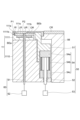
- FIG. 4 is a diagram showing a substrate support and lift mechanism of another exemplary embodiment.
- the substrate support 11 and lift mechanism 50 shown in FIG. 4 can be employed in the plasma processing apparatus 1.
- the embodiment of FIG. 4 will be described below in terms of the differences from the embodiment of FIG. 3.
- the lift mechanism 50 may have a deformation portion 54b that is a contact band instead of a bellows.
- the upper end of the deformation portion 54b may be fixed to the conductive ring 51.
- the lower end of the deformation portion 54b may be fixed to the base 1110.
- the deformation portion 54b shown in FIG. 4 has flexibility in the vertical direction.
- the deformation portion 54b may have a generally arc shape that bulges outward.
- the insulating member IM may provide a recess into which a portion of the deformation portion 54b is disposed.
- FIG. 5 is a diagram showing a substrate processing system according to one exemplary embodiment.
- the substrate processing system PS shown in FIG. 5 includes a transfer module TM, multiple process modules PM1 to PM7 (multiple substrate processing modules), and a controller MC.
- the substrate processing system PS may further include stages LPa to LPd, containers FUa to FUd, a loader module LM, an aligner AN, a load lock module LL1, a load lock module LL2, and a stocker module RSM (ring stocker).
- the number of stages, containers, and load lock modules in the substrate processing system PS may be any number equal to or greater than one.
- the number of process modules in the substrate processing system PS may be any number equal to or greater than two.
- the platforms LPa to LPd are arranged along one edge of the loader module LM.
- the containers FUa to FUd are mounted on the platforms LPa to LPd, respectively.
- Each of the containers FUa to FUd is, for example, a container called a FOUP (Front Opening Unified Pod).
- Each of the containers FUa to FUd is configured to accommodate a substrate W therein.
- the loader module LM has a transfer chamber.
- the pressure in the transfer chamber of the loader module LM is set to atmospheric pressure.
- the loader module LM has a transfer robot LMR.
- the transfer robot LMR is controlled by the controller MC.
- the transfer robot LMR is configured to transfer a substrate W through the transfer chamber of the loader module LM.
- the transfer robot LMR can transfer the substrate W between each of the containers FUa to FUd and the aligner AN, between the aligner AN and each of the load lock modules LL1, LL2, and between each of the load lock modules LL1, LL2 and each of the containers FUa to FUd.
- the aligner AN is connected to the loader module LM.
- the aligner AN is configured to adjust (align) the position of the substrate W.
- the transport module TM has a transport chamber TC (vacuum transport chamber) and a transport robot TR.
- the transport chamber TC is configured so that the space inside it can be depressurized.
- the transport robot TR includes a pick TP (end effector).
- the transport robot TR may include at least two picks TP. In the illustrated example, the transport robot TR includes two picks TP. One of the two picks TP is provided above the other.
- the transport robot TR is configured to transport a substrate W placed on any one of the two picks TP via the transport chamber TC.
- the transport robot TR is controlled by a control unit MC.
- the transfer module TM may be provided with position detection sensors S11 and S12.
- the position detection sensors S11 and S12 are provided on the transfer path of the substrate W and edge ring from the transfer module TM to the process module PM1.
- the position detection sensors S11 and S12 are used to correct the position of the substrate W and edge ring transferred from the transfer module TM to the process module PM1.
- the position detection sensors S11 and S12 are provided, for example, near the gate valve separating the transfer module TM and the process module PM1.
- the position detection sensors S11 and S12 are arranged, for example, such that the distance between them is smaller than the outer diameter of the substrate W and smaller than the inner diameter of the edge ring.
- the transfer module TM may be provided with position detection sensors S21, S22, S31, S32, S41, S42, S51, S52, S61, S62, S71, and S72, similar to the position detection sensors S11 and S12.
- the position detection sensors S21 and S22 are provided on the transport path of the substrate W and edge ring from the transport module TM to the process module PM2.
- the position detection sensors S31 and S32 are provided on the transport path of the substrate W and edge ring from the transport module TM to the process module PM3.
- the position detection sensors S41 and S42 are provided on the transport path of the substrate W and edge ring from the transport module TM to the process module PM4.
- the position detection sensors S51 and S52 are provided on the transport path of the substrate W and edge ring from the transport module TM to the process module PM5.
- the position detection sensors S61 and S62 are provided on the transport path of the substrate W and edge ring from the transport module TM to the process module PM6.
- the position detection sensors S71 and S72 are provided on the transport path of the substrate W and edge ring from the transport module TM to the process module PM7.
- the transport robot TR is configured to transport an edge ring for a substrate support of any one of the process modules PM1 to PM7.
- the edge ring is an edge ring UR or a ring set including an edge ring UR and an edge ring LR.
- the edge ring is placed on any one of the two picks TP and transported.
- Each pick TP has a sensor TS.
- the sensor TS is an optical sensor and configured to measure the position of a ring member such as an edge ring on the substrate support.
- Each of the process modules PM1 to PM7 is an apparatus configured to perform dedicated substrate processing, and has a processing chamber (substrate processing chamber).
- a gate valve is provided between the processing chamber and the transfer chamber TC.
- At least one of the process modules PM1 to PM7 is a plasma processing apparatus 1.
- the stocker module RSM (ring stocker) is connected to the transfer chamber TC via a gate valve.
- the stocker module RSM has a chamber and can accommodate multiple edge rings therein.
- the control unit MC is configured to control each part of the substrate processing system PS.
- the control unit MC may be a computer equipped with a processor, a storage device, an input device, a display device, etc.
- the control unit MC executes a control program stored in the storage device, and controls each part of the substrate processing system PS based on the recipe data stored in the storage device.
- the plasma processing apparatus 1 used as a process module of the substrate processing system PS may include a substrate support 11 as shown in any one of Figures 6 to 9.
- Each of Figures 6 to 9 illustrates a substrate support and a lift mechanism according to yet another exemplary embodiment.
- the edge ring of the plasma processing apparatus 1 can be transported by a transport robot TR and replaced with a corresponding edge ring in the stocker module RSM.
- the substrate support portion 11 provides a plurality of through holes that pass through it in a vertical direction.
- the plurality of through holes in the substrate support portion 11 are arranged in a circumferential direction around the central axis of the substrate support portion 11.
- the plurality of through holes in the substrate support portion 11 may be arranged at equal intervals.
- the edge ring LR is formed with a plurality of through holes that are aligned with the plurality of through holes in the substrate support portion 11.
- the edge ring UR can be lifted upward from the substrate support 11 by a lift mechanism 60.
- the lift mechanism 60 includes a plurality of lift pins 61 and an actuator 62.
- the plurality of lift pins 61 are inserted into a plurality of through holes in the substrate support 11, respectively.
- the actuator 62 is connected to the plurality of lift pins 61 and is configured to move the plurality of lift pins 61 up and down.
- the edge ring UR is lifted upward from the substrate support 11.
- the transport robot TR moves the pick TP below the edge ring UR.
- the edge ring UR is handed over to the pick TP.
- the edge ring UR is then transported to the stocker module RSM by the transport robot TR.
- the replacement edge ring UR is transported from the stocker module RSM into the chamber 10 by the transport robot TR.
- the edge ring UR is then handed over to the multiple lift pins 61 as the multiple lift pins 61 are moved upward by the actuator 62.
- the pick TP then moves outside the chamber 10, and the multiple lift pins 61 move downward.
- the replacement edge ring UR is placed on the substrate support 11.
- the substrate support 11 provides a plurality of through holes passing vertically therethrough.
- the plurality of through holes in the substrate support 11 are arranged circumferentially around the central axis of the substrate support 11.
- the plurality of through holes in the substrate support 11 may be arranged at equal intervals along the circumferential direction.
- the edge ring LR does not have a plurality of through holes that are aligned with the plurality of through holes in the substrate support 11.
- the lift mechanism 70 can lift the ring set including the edge ring UR and the edge ring LR upward from the substrate support 11.
- the lift mechanism 70 includes a plurality of lift pins 71 and an actuator 72.
- the plurality of lift pins 71 are inserted into a plurality of through holes in the substrate support 11, respectively.
- the actuator 72 is connected to the plurality of lift pins 71 and is configured to move the plurality of lift pins 71 up and down.
- the ring set is lifted upward from the substrate support portion 11.
- the transport robot TR moves the pick TP below the ring set.
- the ring set is handed over to the pick TP.
- the ring set is then transported to the stocker module RSM by the transport robot TR.
- the replacement ring set is transported from the stocker module RSM into the chamber 10 by the transport robot TR.
- the multiple lift pins 71 are then moved upward by the actuator 72, and the ring set is handed over to the multiple lift pins 71.
- the pick TP then moves outside the chamber 10, and the multiple lift pins 71 move downward. This places the replacement ring set on the substrate support 11.
- the conductive ring 51 extends to a region on the edge ring LR so as to support the edge ring UR by its upper inner edge.
- an outer ring OR is disposed on the conductive ring 51 so as to surround the edge ring UR.
- the outer ring OR may be formed of an insulating material such as quartz.
- the substrate support 11 also provides a plurality of through holes passing therethrough. The plurality of through holes in the substrate support 11 are arranged in a circumferential direction around the central axis of the substrate support 11. The plurality of through holes in the substrate support 11 may be arranged at equal intervals in a circumferential direction.
- the edge ring LR is formed with a plurality of through holes that are aligned with the plurality of through holes in the substrate support 11.
- the operation of the lift mechanism 60 and the transport robot TR for replacing the edge ring UR in the embodiment of FIG. 8 is similar to the operation of the lift mechanism 60 and the transport robot TR for replacing the edge ring UR in the embodiment of FIG. 6.
- the edge ring LR has an outer diameter smaller than the outer diameter of the edge ring UR.
- the edge ring UR is disposed on the edge ring LR such that its outer edge protrudes radially outward relative to the edge ring LR.
- the conductive ring 51 supports the outer edge of the edge ring UR by its upper inner edge.
- an outer ring OR is disposed on the conductive ring 51 so as to surround the edge ring UR.
- the outer ring OR may be formed from an insulating material such as quartz.
- another outer ring BOR is disposed below the upper end of the conductive ring 51 so as to surround the edge ring LR.
- the outer ring BOR may be formed from an insulating material such as quartz.
- the substrate support 11 provides a plurality of through holes passing therethrough, similar to the embodiment of FIG. 7.
- the plurality of through holes in the substrate support 11 are arranged circumferentially around the central axis of the substrate support 11.
- the plurality of through holes in the substrate support 11 may be equally spaced apart in the circumferential direction.
- the edge ring LR does not have a plurality of through holes that are aligned with the plurality of through holes in the substrate support 11.
- the operation of the lift mechanism 70 and the transport robot TR for replacing the edge ring in the embodiment of FIG. 9 is similar to the operation of the lift mechanism 70 and the transport robot TR for replacing the edge ring in the embodiment of FIG. 7.
- the plasma processing apparatus 1 may be configured to selectively replace only the edge ring UR and replace the above-mentioned ring set.
- the plasma processing apparatus 1 may have both the lift mechanism 60 and the lift mechanism 70.
- the multiple lift pins 61 and the multiple lift pins 71 are arranged alternately along the circumferential direction. Above each of the multiple lift pins 71, no through-hole is formed in the edge ring LR.
- FIG. 10 is a diagram for explaining a configuration example of a capacitively coupled plasma processing apparatus.
- the plasma processing apparatus 1 shown in FIG. 10 includes a substrate support portion 11 and a lift mechanism 50 of a plasma processing apparatus according to any one of the various exemplary embodiments described above.
- the plasma processing apparatus 1 shown in FIG. 10 may include the lift mechanism 60 and/or the lift mechanism 70 described above.
- the plasma processing apparatus 1 shown in FIG. 10 may also be employed as a process module in a substrate processing system PS.
- the capacitively coupled plasma processing apparatus 1 shown in FIG. 10 will be described from the viewpoint of differences from the inductively coupled plasma processing apparatus 1 shown in FIG. 2.
- the gas introduction section includes a shower head 13A.
- the shower head 13A is disposed above the substrate support section 11.
- the shower head 13A constitutes at least a part of the ceiling of the plasma processing chamber 10.
- the plasma processing chamber 10 has a plasma processing space 10s defined by the shower head 13A, a sidewall 10a of the plasma processing chamber 10, and the substrate support section 11.
- the plasma processing chamber 10 is grounded.
- the shower head 13A and the substrate support section 11 are electrically insulated from the housing of the plasma processing chamber 10.
- the shower head 13A is configured to introduce at least one processing gas from the gas supply unit 20 into the plasma processing space 10s.
- the shower head 13A has at least one gas supply port 13Aa, at least one gas diffusion chamber 13Ab, and multiple gas inlets 13Ac.
- the processing gas supplied to the gas supply port 13Aa passes through the gas diffusion chamber 13Ab and is introduced into the plasma processing space 10s from the multiple gas inlets 13Ac.
- the shower head 13A also includes at least one upper electrode.
- the gas introduction unit may include, in addition to the shower head 13A, one or more side gas injectors (SGI) attached to one or more openings formed in the sidewall 10a.
- SGI side gas injectors
- the DC power supply 32 may further include a second DC generating unit 32b in addition to the bias DC generating unit 32a, i.e., the first DC generating unit 32a.
- the first DC generating unit 32a is connected to at least one lower electrode and configured to generate a first DC signal.
- the generated first DC signal is applied to at least one lower electrode.
- the second DC generating unit 32b is connected to at least one upper electrode and configured to generate a second DC signal.
- the generated second DC signal is applied to at least one upper electrode.
- a second DC signal may be pulsed.
- a sequence of voltage pulses is applied to at least one lower electrode and/or at least one upper electrode.
- the voltage pulses may have a rectangular, trapezoidal, triangular or combination thereof pulse waveform.
- a waveform generator for generating a sequence of voltage pulses from the DC signal is connected between the first DC generator 32a and at least one lower electrode.
- the first DC generator 32a and the waveform generator constitute a voltage pulse generator.
- the voltage pulse generator is connected to at least one upper electrode.
- the voltage pulses may have a positive polarity or a negative polarity.
- the sequence of voltage pulses may include one or more positive polarity voltage pulses and one or more negative polarity voltage pulses within one period.
- the first and second DC generating units 32a and 32b may be provided in addition to the RF power source 31, or the first DC generating unit 32a may be provided in place of the second RF generating unit 31b.
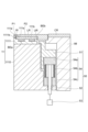
- FIG. 11 is a diagram showing a substrate support and lift mechanism according to yet another exemplary embodiment.
- the substrate support 11 and lift mechanism 50 shown in FIG. 11 can be employed in the inductively coupled plasma processing apparatus 1 or the capacitively coupled plasma processing apparatus 1 described above. Below, the substrate support 11 and lift mechanism 50 shown in FIG. 11 will be described from the perspective of the differences from the substrate support 11 and lift mechanism 50 shown in FIG. 3.
- the lift mechanism 50 shown in FIG. 11 can electrically couple (e.g., conduct) the conductive ring 51 to the edge ring UR while the edge ring UR on the conductive ring 51 is supported by the conductive ring 51. That is, the lift mechanism 50 shown in FIG. 11 can also form a first state in which the edge ring UR and the base 1110 are electrically coupled to each other (e.g., a conductive state between the edge ring UR and the base 1110). The lift mechanism 50 shown in FIG. 11 can also lower the conductive ring 51 downward via the rod 52 by the actuator 53, thereby separating the conductive ring 51 from the edge ring UR. That is, the lift mechanism 50 shown in FIG.
- the lift mechanism 50 shown in FIG. 11 constitutes a switch that is configured to be able to switch between the first state and the second state.
- FIG. 12 is a diagram showing a substrate support and lift mechanism according to yet another exemplary embodiment.
- the substrate support 11 and lift mechanism 50 shown in FIG. 12 can be employed in the inductively coupled plasma processing apparatus 1 or the capacitively coupled plasma processing apparatus 1 described above. Below, the substrate support 11 and lift mechanism 50 shown in FIG. 12 will be described from the perspective of the differences from the substrate support 11 and lift mechanism 50 shown in FIG. 4.
- the plasma processing apparatus 1 including the lift mechanism 50 shown in FIG. 12 further includes a switch 56.
- the switch 56 may be part of the lift mechanism 50.
- the switch 56 includes a switching element and is connected between the connection member 54 and the conductive ring 51 or between the connection member 54 and the base 1110.
- a first state e.g., a conductive state between the edge ring UR and the base 1110 in which the edge ring UR and the base 1110 are electrically coupled to each other is formed.
- FIG. 13 is a diagram showing a substrate support and lift mechanism according to yet another exemplary embodiment.
- the substrate support 11 and lift mechanism 50 shown in FIG. 13 can be employed in the inductively coupled plasma processing apparatus 1 or the capacitively coupled plasma processing apparatus 1 described above. Below, the substrate support 11 and lift mechanism 50 shown in FIG. 13 will be described from the perspective of the differences from the substrate support 11 and lift mechanism 50 shown in FIG. 6.
- the plasma processing apparatus 1 including the lift mechanism 50 shown in FIG. 13 includes a lift mechanism 60 as a switch configured to be able to switch between the first state and the second state described above.
- all the lift pins 61 are made of an insulating material.
- a first state e.g., a conductive state between the edge ring UR and the base 1110 is formed.
- a second state (e.g., a non-conductive state between the edge ring UR and the base 1110) is formed.
- the switch described with reference to Figs. 11 to 13 makes it possible to switch between the first state and the second state as necessary.
- the switch can be controlled by the control unit 2.
- Figs. 14 to 18 a plasma processing method performed in the plasma processing apparatus 1 including the switch shown in Figs. 11 to 13 will be described.
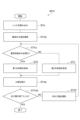
- FIG. 14 is a flow chart showing a plasma processing method according to one exemplary embodiment.
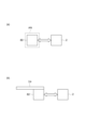
- FIG. 15(a) is a diagram showing an example of an imaging device used with a plasma processing apparatus according to various exemplary embodiments.
- an imaging device 80 shown in FIG. 15(a) may be used.
- the imaging device 80 may be disposed in the aligner AN.
- the imaging device 80 may be disposed in any location as long as it is capable of acquiring an image of the substrate W.
- the method MT is performed with the substrate W placed on the substrate support 11.
- the method MT starts with step STa.
- step STa the recipe is read by the control unit 2.
- the control unit 2 determines whether electrical connection (e.g., conduction) between the edge ring UR and the base 1110 is necessary. In process STJ, if the control unit 2 determines that the plasma density on the edge ring UR should be increased, it may determine that electrical connection between the edge ring UR and the base 1110 is necessary. On the other hand, in process STJ, if the control unit 2 determines that the plasma density on the edge ring UR should not be increased, it may determine that electrical connection between the edge ring UR and the base 1110 is not necessary.
- electrical connection e.g., conduction
- control unit 2 determines that the plasma density on the edge ring UR should be increased, it controls the switch to form a first state (e.g., a conductive state between the edge ring UR and the base 1110) in step STb.
- control unit 2 determines that the plasma density on the edge ring UR should not be increased, it controls the switch to form a second state (e.g., a non-conductive state between the edge ring UR and the base 1110) in step STc.
- process STd is performed.
- the control unit 2 controls each part of the plasma processing apparatus 1 so as to perform plasma processing according to the above-mentioned recipe.
- the edge ring UR and the base 1110 are electrically coupled to each other (for example, they are conductive to each other)
- the plasma density on the edge ring UR increases due to the source RF signal and/or electrical bias supplied from the base 1110 to the edge ring UR via the conductive ring 51.
- the control unit 2 may obtain, from the imaging device 80, an image of the upper surface of the substrate W that has been processed using the same recipe in the plasma processing device 1 before the substrate W placed on the substrate support 11 for the purpose of judgment in the step STJ.
- the control unit 2 may determine whether or not the density of the plasma on the edge ring UR should be increased based on this image.
- a plurality of holes may be formed in the substrate W by the plasma processing based on the recipe. In this case, when the control unit 2 determines in the step STJ from the image obtained from the imaging device 80 that the circularity of the hole in the edge region and the upper surface of the substrate W is equal to or less than the threshold value, it performs the step STb.
- control unit 2 determines in the step STJ from the image obtained from the imaging device 80 that the circularity is greater than the threshold value, it performs the step STc.
- the circularity may be the ratio of the minimum width to the maximum width of the hole in the edge region and the upper surface of the substrate W.
- FIG. 15(b) illustrates an example of a measuring device used with a plasma processing apparatus according to various exemplary embodiments.
- a measuring device 82 shown in FIG. 15(b) may be used.
- the measuring device 82 is attached to a pick TP.
- the measuring device 82 is configured to measure the thickness of the deposit on the edge ring UR.
- the measuring device 82 may include an image sensor that captures an image of the edge ring UR, or may include other optical sensors that are configured to measure the thickness of the deposit on the edge ring UR.
- the control unit 2 may determine whether or not to increase the density of the plasma on the edge ring UR according to the thickness of the deposit on the edge ring UR measured by the measuring device 82.
- the inside of the chamber 10 is cleaned by a plasma process based on a recipe.
- the control unit 2 determines in the process STJ that the thickness of the deposit on the edge ring UR measured by the measuring device 82 is equal to or greater than the threshold value, the control unit 2 performs the process STb.
- the control unit 2 determines in the process STJ that the thickness of the deposit on the edge ring UR measured by the measuring device 82 is smaller than the threshold value, the control unit 2 performs the process STc.
- the process STd When the process STd is performed after the process STb, the density of the plasma on the edge ring UR is increased, and the removal of the deposit on the edge ring UR is promoted.
- a cleaning gas containing an oxygen-containing gas such as O2 gas or other gas is used, and cleaning can be performed by the plasma generated from the cleaning gas.
- no object may be placed on the central region 111a of the substrate support 11, and a dummy wafer may be placed on the central region 111a.
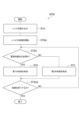
- FIG. 16 is a flow chart showing a plasma processing method according to another exemplary embodiment.
- the plasma processing method shown in FIG. 16 (hereinafter referred to as "method MTA") starts with step STa, which is similar to step STa of method MT.
- Method MTA is performed with the substrate W placed on the substrate support 11.
- the control unit 2 selects the first process specified in the recipe.
- the recipe includes multiple processes, and the recipe specifies setting information regarding the electrical connection (e.g., conductivity) between the edge ring UR and the base 1110 for each process.
- the setting information is information that specifies the first state (e.g., conductive state) or the second state (e.g., non-conductive state) described above.
- the control unit 2 determines whether electrical connection between the edge ring UR and the base 1110 is necessary from the setting information specified in the recipe for the selected process. If the control unit 2 determines that electrical connection between the edge ring UR and the base 1110 is necessary in process STAJ, it performs process STb in the same manner as method MT. On the other hand, if the control unit 2 determines that electrical connection between the edge ring UR and the base 1110 is not necessary in process STAJ, it performs process STc in the same manner as method MT. Then, the control unit 2 controls each part of the plasma processing apparatus 1 to perform the process selected in process STAe.
- control unit 2 determines whether or not all processes included in the recipe have been completed. If the control unit 2 determines that all processes have not been completed, it selects the next process included in the recipe in process STAf and continues processing from process STAJ. On the other hand, if the control unit 2 determines that all processes have been completed in process STAJb, it ends the method MTA.
- Figure 17 is a flow chart showing a plasma processing method according to yet another exemplary embodiment.
- Figure 18 is a diagram showing an example of a measuring device used with plasma processing apparatuses according to various exemplary embodiments.
- a measuring device 200 shown in Figure 18 can be used.
- the measuring device 200 includes a focusing lens 202, an optical fiber 204, a light source 206, a photodetector 208, and a calculation unit 210.
- the focusing lens 202 is provided above the ceiling 10U of the chamber 10, and is optically coupled to the substrate W on the substrate support 11 via an optical window in the ceiling 10U.
- the ceiling 10U is the dielectric window 101 or the shower head 13A.
- the condenser lens 202 is optically connected to a light source 206 and a photodetector 208 (polychrometer) via an optical fiber 204.
- the light source 206 emits light Ls.
- the light Ls emitted from the light source 206 is irradiated onto the substrate W via the optical fiber 204 and the condenser lens 202.
- the light Ls is reflected at multiple points in the substrate W at different height positions, generating interference light Li.
- the interference light Li is input to the photodetector 208 via the condenser lens 202 and the optical fiber 204.
- the photodetector 208 is configured to detect the light intensity of the interference light Li.
- the calculation unit 210 is configured to measure the etching depth of the substrate W based on the change in the light intensity of the interference light Li detected by the photodetector 208.
- the light intensity of the interference light Li changes periodically according to the etching depth of the substrate W. Therefore, the calculation unit 210 can identify the etching depth of the substrate W from the change in the light intensity of the interference light Li.
- step STa which is the same as step STa of method MT.
- Method MTB is performed with the substrate W placed on the substrate support 11.
- the control unit 2 starts plasma processing according to the recipe, specifically, plasma etching of the substrate W.
- the control unit 2 controls each part of the plasma processing apparatus 1 according to the recipe.
- a second state e.g., a non-conductive state between the edge ring UR and the base 1110 is formed.
- Steps STBJ to STBJb are performed during the period in which the plasma etching started in step STBd is being performed.
- the control unit 2 determines whether electrical connection (e.g., conduction) between the edge ring UR and the base 1110 is necessary. Specifically, the control unit 2 determines whether the etching depth measured by the measuring device 200 has reached a threshold value. If the control unit 2 determines that the etching depth has reached the threshold value, it performs step STb. On the other hand, if the control unit 2 determines that the etching depth has not reached the threshold value, it performs step STc and maintains the second state (e.g., non-conductive state).
- the second state e.g., non-conductive state
- step STBJb it is determined whether or not to terminate the process started in step STd, i.e., plasma etching. If plasma etching is not to be terminated, the process is repeated from step STBJ. On the other hand, if plasma etching is to be terminated, the control unit 2 terminates method MTB.
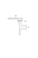
- FIG. 19 is a diagram showing an edge ring and a conductive ring according to yet another exemplary embodiment.
- the conductive ring 51 may contact the edge ring UR and be conductive with the edge ring UR to form a conductive state between the edge ring UR and the base 1110 as a first state.
- the conductive ring 51 may be conductive with the edge ring UR via a member 51c to form a conductive state between the edge ring UR and the base 1110 as a first state.
- the member 51c is made of a conductive material such as a metal. When the first state is formed, the member 51c is sandwiched between the edge ring UR and the conductive ring 51.
- the member 51c may have elasticity.
- the member 51c may be a diagonally wound coil spring.
- FIG. 20 is a diagram showing an edge ring and a conductive ring according to yet another exemplary embodiment.
- the conductive ring 51 may form a first state by capacitively coupling to the edge ring UR.
- the conductive ring 51 may include a dielectric region 51f on its upper surface.
- the conductive ring 51 capacitively couples to the edge ring UR while supporting the edge ring UR placed on the dielectric region 51f.
- the dielectric region 51f may be a film formed from a dielectric material.
- the dielectric region 51f may cover the surface of the conductive ring 51.
- the dielectric region 51f may be formed by thermal spraying of a material such as yttrium oxide.
- FIG. 21 illustrates a substrate support and a lift mechanism according to yet another exemplary embodiment.
- the edge ring UR and the edge ring LR may have the structure shown in FIG. 21.
- the edge ring LR includes an inner periphery LRi, an intermediate portion LRm, and an outer periphery LRo.
- the inner periphery LRi is ring-shaped and is disposed on the ring support surface along the side wall surface 111s.
- the edge region of the substrate W is located above the inner periphery LRi.
- the outer periphery LRo is ring-shaped and extends radially outward relative to the inner periphery LRi.
- the edge ring UR is disposed on the outer periphery LRo.
- the intermediate portion LRm is ring-shaped and extends between the inner periphery LRi and the outer periphery LRo.
- the intermediate portion LRm is interposed between the edge of the substrate W on the substrate support surface and the inner periphery of the edge ring UR.
- the height position of the upper surface of the intermediate portion LRm is higher than the height position of the upper surface of the inner peripheral portion LRi and the height position of the upper surface of the outer peripheral portion LRo.
- the intermediate portion LRm may have a thickness greater than the thickness of the inner peripheral portion LRi and the thickness of the outer peripheral portion LRo.
- the edge ring UR When the edge ring UR is placed on the edge ring LR in contact with the edge ring LR, the edge ring UR exchanges heat with the base 1110 via the edge ring LR and the electrostatic chuck 1111.
- the edge ring UR when the edge ring UR is raised upward relative to the edge ring LR, the temperature of the edge ring UR may rise.
- the intermediate portion LRm as shown in FIG. 21, the inner peripheral surface of the edge ring UR is separated from the edge of the substrate W by a distance D in the radial direction. Therefore, even if the temperature of the edge ring UR rises, the temperature of the edge region of the substrate W is suppressed from rising.
- the difference between the upper end position of the plasma sheath on the substrate W and the upper end position of the plasma sheath on the edge ring UR can be reduced.
- ions can be supplied vertically to the edge region of the substrate W to vertically form a recess such as a hole in the edge region of the substrate W.
- the distance D may be 10 mm or less, 6 mm or less, or approximately 6 mm.
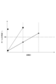
- FIG. 22 is a graph showing the results of the experiment.
- the horizontal axis indicates the drive amount of the conductive ring 51.
- the drive amount is 0.
- the drive amount is larger as the edge ring UR is raised upward from the edge ring LR and the vertical distance between the edge ring UR and the edge ring LR is larger.
- the vertical axis indicates the hole angle.
- the rectangular plot is the hole angle obtained when a non-worn edge ring UR is used in the plasma processing apparatus 1 having the configuration shown in FIG. 3 and the drive amount is 0.
- FIG. 22 the horizontal axis indicates the drive amount of the conductive ring 51.
- any of the above-mentioned containers FUa to FUd may be used as the stocker module RSM.
- a chamber a substrate support disposed within the chamber; an edge ring having electrical conductivity and disposed to surround the substrate on the substrate support; a lift mechanism configured to move the edge ring up and down;
- a plasma generating unit including a high frequency power source and configured to generate plasma in the chamber; a bias power supply configured to generate an electrical bias to attract ions from the plasma to the substrate on the substrate support; Equipped with
- the substrate support includes: a base electrically coupled to the bias power supply and/or the high frequency power supply; an electrostatic chuck on the base; Including,
- the lift mechanism includes: a conductive ring that is electrically coupled to the edge ring while supporting the edge ring placed thereon; a rod extending vertically below the conductive ring; an actuator configured to move the edge ring up and down via the rod and the conductive ring; a connecting member providing an electrical connection between the conductive ring and the base, the connecting member being configured to maintain the electrical connection in response to movement of the conductive ring; and Including, Plasma processing equipment.
- connection member includes a bellows, a contact band, or a cylindrical member having a plurality of slits formed in a side wall surface thereof so as to be elastically deformable in the longitudinal direction.
- the edge ring is a top edge ring;
- the plasma processing apparatus further comprises a lower edge ring on which the upper edge ring is disposed;
- the electrostatic chuck comprises: a first portion having a substrate support surface; a second portion having a ring support surface extending below the substrate support surface and extending outwardly of the first portion; Including, the first portion includes a sidewall surface extending between the substrate support surface and the ring support surface; the lower edge ring is disposed along the sidewall surface and on the ring support surface.
- the lower edge ring is an inner periphery disposed along the side wall surface; an outer periphery extending radially outwardly from the inner periphery and on which the upper edge ring is disposed; an intermediate portion extending between the inner periphery and the outer periphery and interposed between an edge of a substrate on the substrate support surface and an inner periphery of the upper edge ring; Including, The plasma processing apparatus according to E6.
- E11 The plasma processing apparatus described in any one of E1 to E10, further comprising a switch configured to be able to switch between a first state in which the edge ring and the base are electrically coupled to each other and a second state in which the edge ring and the base are electrically isolated from each other.
- E15 The plasma processing apparatus of E11, further comprising a control unit configured to control the switch to form the first state or the second state according to a loaded recipe.
- E16 a measurement device configured to measure an etch depth of a substrate on the substrate support; a controller configured to control the switch to switch from the second state to the first state when the etching depth measured by the measuring device reaches a threshold value;
- the plasma processing apparatus of E11 further comprising:
- E10 The plasma processing apparatus according to E10, a transfer module including a transfer chamber and a transfer robot connected to the plasma processing apparatus; a ring stocker configured to accommodate the upper edge ring or the upper edge ring and the ring set therein; A control unit; Equipped with the control unit is configured to control the separate lift mechanism and the transfer robot to exchange the upper edge ring or the ring set in the chamber of the plasma processing apparatus with the upper edge ring or the ring set in the chamber via the transfer chamber. Substrate processing system.
- a plasma processing apparatus an imaging device configured to capture an image of a substrate etched by the plasma processing device;
- a control unit; Equipped with the control unit is configured to control the switch to form the first state when etching the substrate later in the plasma processing apparatus when the circularity of a hole in an edge region of a previously processed substrate is equal to or less than a threshold value from the image of the substrate.
- E11 a plasma processing apparatus according to the present invention; a gage configured to measure a thickness of the edge ring deposit; and A control unit; Equipped with the control unit is configured to control the switch to form the second state when a thickness of the deposit is smaller than a threshold value during a cleaning process in the chamber, and to form the first state when a thickness of the deposit is equal to or greater than the threshold value.
- Substrate processing system a plasma processing apparatus according to the present invention.
- 1...plasma processing apparatus 10...chamber, 11...substrate support section, 12...plasma generation section, 1110...base, 1111...electrostatic chuck, 50...lift mechanism, 51...conductive ring, 52...rod, 53...actuator, 54...connecting member, PS...substrate processing system, TM...transport module, RSM...stocker module, MC...control section.
Landscapes
- Chemical & Material Sciences (AREA)
- Physics & Mathematics (AREA)
- Engineering & Computer Science (AREA)
- Plasma & Fusion (AREA)
- Analytical Chemistry (AREA)
- Mechanical Engineering (AREA)
- Chemical Kinetics & Catalysis (AREA)
- Materials Engineering (AREA)
- General Chemical & Material Sciences (AREA)
- Metallurgy (AREA)
- Organic Chemistry (AREA)
- Electromagnetism (AREA)
- Spectroscopy & Molecular Physics (AREA)
- Container, Conveyance, Adherence, Positioning, Of Wafer (AREA)
- Chemical Vapour Deposition (AREA)
- Drying Of Semiconductors (AREA)
Abstract
Description
チャンバと、
前記チャンバ内に配置された基板支持部と、
導電性を有し、前記基板支持部上の基板を囲むように配置されるエッジリングと、
前記エッジリングを上下に移動させるように構成されたリフト機構と、
高周波電源を含み、前記チャンバ内でプラズマを生成するように構成されたプラズマ生成部と、
前記基板支持部上の前記基板に前記プラズマからイオンを引き込むために電気バイアスを発生するように構成されたバイアス電源と、
を備え、
前記基板支持部は、
前記バイアス電源及び/又は前記高周波電源と電気的に結合された基台と、
該基台上の静電チャックと、
を含み、
前記リフト機構は、
その上に載置される前記エッジリングを支持した状態で該エッジリングに電気的に結合する導電リングと、
前記導電リングの下方で鉛直方向に延びるロッドと、
前記ロッド及び前記導電リングを介して前記エッジリングを上下に移動させるように構成されたアクチュエータと、
前記導電リングと前記基台との間の電気的接続を提供する接続部材であり、前記導電リングの移動に応じて該電気的接続を維持するように構成された、該接続部材と、
を含む、
プラズマ処理装置。
前記接続部材は、前記導電リングの移動に応じて変形可能である、E1に記載のプラズマ処理装置。
前記接続部材は、ベローズ、コンタクトバンド、又はその長手方向において弾性変形可能であるように複数のスリットがその側壁面に形成された筒状の部材を含む、E2に記載のプラズマ処理装置。
前記ロッドは、絶縁性を有する、E1~E3の何れか一項に記載のプラズマ処理装置。
前記導電リングの表面において露出されている領域は、前記プラズマに対して耐性を有する膜によって覆われている、E1~E4の何れか一項に記載のプラズマ処理装置。
前記エッジリングは、上部エッジリングであり、
該プラズマ処理装置は、その上に前記上部エッジリングが配置される下部エッジリングを更に備え、
前記静電チャックは、
基板支持面を有する第1部分と、
前記基板支持面よりも低い位置で延在するリング支持面を有し、前記第1部分の外側で延在する第2部分と、
を含み、
前記第1部分は、前記基板支持面と前記リング支持面との間で延びる側壁面を含み、
前記下部エッジリングは、前記側壁面に沿って、且つ、前記リング支持面上に配置される、
E1~E5の何れか一項に記載のプラズマ処理装置。
前記下部エッジリングは、
前記側壁面に沿って配置される内周部と、
前記内周部に対して径方向外側で延在し、その上に前記上部エッジリングが配置される外周部と、
前記内周部と前記外周部との間で延在し、前記基板支持面上の基板のエッジと前記上部エッジリングの内周面との間に介在する中間部と、
を含む、
E6に記載のプラズマ処理装置。
前記下部エッジリングは導電性を有する、E6又はE7に記載のプラズマ処理装置。
前記下部エッジリングは絶縁性を有する、E6又はE7に記載のプラズマ処理装置。
前記上部エッジリング又は前記上部エッジリングと前記下部エッジリングを含むリングセットを前記静電チャックから持ち上げるように構成された別のリフト機構を更に備える、E6~E9の何れか一項に記載のプラズマ処理装置。
前記エッジリングと前記基台とが互いに電気的に結合される第1の状態と前記エッジリングと前記基台とが互いから電気的に分離される第2の状態を切り替え可能に構成された切替器を更に備える、E1~E10の何れか一項に記載のプラズマ処理装置。
前記リフト機構は、前記切替器であり、前記エッジリングから前記導電リングを引き離すように前記導電リングを前記アクチュエータによって降下させることにより前記第2の状態を形成するように構成されている、E11に記載のプラズマ処理装置。
前記切替器は、前記接続部材と前記導電リングとの間又は前記接続部材と前記基台との間で接続されたスイッチング素子を含む、E11に記載のプラズマ処理装置。
前記切替器は、前記エッジリングを前記導電リングから持ち上げることにより前記第2の状態を形成するように構成された別のリフト機構を含む、E11に記載のプラズマ処理装置。
読み込んだレシピに従って前記第1の状態又は前記第2の状態を形成するよう前記切替器を制御するように構成された制御部を更に備える、E11に記載のプラズマ処理装置。
前記基板支持部上の基板のエッチング深さを測定するように構成された測定器と、
前記測定器によって測定された前記エッチング深さが閾値に到達したときに前記第2の状態から前記第1の状態に切り替えるよう前記切替器を制御するように構成された制御部と、
を更に備えるE11に記載のプラズマ処理装置。
E10に記載のプラズマ処理装置と、
前記プラズマ処理装置に接続された搬送チャンバ及び搬送ロボットを含む搬送モジュールと、
前記上部エッジリング又は前記上部エッジリングと前記リングセットをその中に収容可能に構成されたリングストッカと、
制御部と、
を備え、
前記制御部は、前記別のリフト機構及び前記搬送ロボットを制御して、前記プラズマ処理装置の前記チャンバ内の前記上部エッジリング又は前記リングセットを、前記チャンバ内の前記上部エッジリング又は前記リングセットと、前記搬送チャンバを介して交換するように構成されている、
基板処理システム。
E11に記載のプラズマ処理装置と、
前記プラズマ処理装置によってエッチングされた基板の画像を取得するように構成された撮像装置と、
制御部と、
を備え、
前記制御部は、先に処理された基板の前記画像から該基板のエッジ領域におけるホールの真円度が閾値以下である場合に、前記プラズマ処理装置において後に基板に対してエッチングを行う際に、前記第1の状態を形成するよう前記切替器を制御するように構成されている、
基板処理システム。
E11に記載のプラズマ処理装置と、
前記エッジリングの堆積物の厚さを測定するように構成された測定器と、
制御部と、
を備え、
前記制御部は、前記チャンバ内でのクリーニング処理の際に、前記堆積物の厚さが閾値よりも小さい場合には前記第2の状態を形成し、前記堆積物の厚さが前記閾値以上である場合には前記第1の通状態を形成するよう前記切替器を制御するように構成されている、
基板処理システム。
Claims (19)
- チャンバと、
前記チャンバ内に配置された基板支持部と、
導電性を有し、前記基板支持部上の基板を囲むように配置されるエッジリングと、
前記エッジリングを上下に移動させるように構成されたリフト機構と、
高周波電源を含み、前記チャンバ内でプラズマを生成するように構成されたプラズマ生成部と、
前記基板支持部上の前記基板に前記プラズマからイオンを引き込むために電気バイアスを発生するように構成されたバイアス電源と、
を備え、
前記基板支持部は、
前記バイアス電源及び/又は前記高周波電源と電気的に結合された基台と、
該基台上の静電チャックと、
を含み、
前記リフト機構は、
その上に載置される前記エッジリングを支持した状態で該エッジリングに電気的に結合する導電リングと、
前記導電リングの下方で鉛直方向に延びるロッドと、
前記ロッド及び前記導電リングを介して前記エッジリングを上下に移動させるように構成されたアクチュエータと、
前記導電リングと前記基台との間の電気的接続を提供する接続部材であり、前記導電リングの移動に応じて該電気的接続を維持するように構成された、該接続部材と、
を含む、
プラズマ処理装置。 - 前記接続部材は、前記導電リングの移動に応じて変形可能である、請求項1に記載のプラズマ処理装置。
- 前記接続部材は、ベローズ、コンタクトバンド、又はその長手方向において弾性変形可能であるように複数のスリットがその側壁面に形成された筒状の部材を含む、請求項2に記載のプラズマ処理装置。
- 前記ロッドは、絶縁性を有する、請求項1~3の何れか一項に記載のプラズマ処理装置。
- 前記導電リングの表面において露出されている領域は、前記プラズマに対して耐性を有する膜によって覆われている、請求項1~3の何れか一項に記載のプラズマ処理装置。
- 前記エッジリングは、上部エッジリングであり、
該プラズマ処理装置は、その上に前記上部エッジリングが配置される下部エッジリングを更に備え、
前記静電チャックは、
基板支持面を有する第1部分と、
前記基板支持面よりも低い位置で延在するリング支持面を有し、前記第1部分の外側で延在する第2部分と、
を含み、
前記第1部分は、前記基板支持面と前記リング支持面との間で延びる側壁面を含み、
前記下部エッジリングは、前記側壁面に沿って、且つ、前記リング支持面上に配置される、
請求項1~3の何れか一項に記載のプラズマ処理装置。 - 前記下部エッジリングは、
前記側壁面に沿って配置される内周部と、
前記内周部に対して径方向外側で延在し、その上に前記上部エッジリングが配置される外周部と、
前記内周部と前記外周部との間で延在し、前記基板支持面上の基板のエッジと前記上部エッジリングの内周面との間に介在する中間部と、
を含む、
請求項6に記載のプラズマ処理装置。 - 前記下部エッジリングは導電性を有する、請求項6に記載のプラズマ処理装置。
- 前記下部エッジリングは絶縁性を有する、請求項6に記載のプラズマ処理装置。
- 前記上部エッジリング又は前記上部エッジリングと前記下部エッジリングを含むリングセットを前記静電チャックから持ち上げるように構成された別のリフト機構を更に備える、請求項6に記載のプラズマ処理装置。
- 前記エッジリングと前記基台とが互いに電気的に結合される第1の状態と前記エッジリングと前記基台とが互いから電気的に分離される第2の状態を切り替え可能に構成された切替器を更に備える、請求項1~3の何れか一項に記載のプラズマ処理装置。
- 前記リフト機構は、前記切替器であり、前記エッジリングから前記導電リングを引き離すように前記導電リングを前記アクチュエータによって降下させることにより前記第2の状態を形成するように構成されている、請求項11に記載のプラズマ処理装置。
- 前記切替器は、前記接続部材と前記導電リングとの間又は前記接続部材と前記基台との間で接続されたスイッチング素子を含む、請求項11に記載のプラズマ処理装置。
- 前記切替器は、前記エッジリングを前記導電リングから持ち上げることにより前記第2の状態を形成するように構成された別のリフト機構を含む、請求項11に記載のプラズマ処理装置。
- 読み込んだレシピに従って前記第1の状態又は前記第2の状態を形成するよう前記切替器を制御するように構成された制御部を更に備える、請求項11に記載のプラズマ処理装置。
- 前記基板支持部上の基板のエッチング深さを測定するように構成された測定器と、
前記測定器によって測定された前記エッチング深さが閾値に到達したときに前記第2の状態から前記第1の状態に切り替えるよう前記切替器を制御するように構成された制御部と、
を更に備える請求項11に記載のプラズマ処理装置。 - 請求項10に記載のプラズマ処理装置と、
前記プラズマ処理装置に接続された搬送チャンバ及び搬送ロボットを含む搬送モジュールと、
前記上部エッジリング又は前記上部エッジリングと前記リングセットをその中に収容可能に構成されたリングストッカと、
制御部と、
を備え、
前記制御部は、前記別のリフト機構及び前記搬送ロボットを制御して、前記プラズマ処理装置の前記チャンバ内の前記上部エッジリング又は前記リングセットを、前記チャンバ内の前記上部エッジリング又は前記リングセットと、前記搬送チャンバを介して交換するように構成されている、
基板処理システム。 - 請求項11に記載のプラズマ処理装置と、
前記プラズマ処理装置によってエッチングされた基板の画像を取得するように構成された撮像装置と、
制御部と、
を備え、
前記制御部は、先に処理された基板の前記画像から該基板のエッジ領域におけるホールの真円度が閾値以下である場合に、前記プラズマ処理装置において後に基板に対してエッチングを行う際に、前記第1の状態を形成するよう前記切替器を制御するように構成されている、
基板処理システム。 - 請求項11に記載のプラズマ処理装置と、
前記エッジリングの堆積物の厚さを測定するように構成された測定器と、
制御部と、
を備え、
前記制御部は、前記チャンバ内でのクリーニング処理の際に、前記堆積物の厚さが閾値よりも小さい場合には前記第2の状態を形成し、前記堆積物の厚さが前記閾値以上である場合には前記第1の状態を形成するよう前記切替器を制御するように構成されている、
基板処理システム。
Priority Applications (8)
| Application Number | Priority Date | Filing Date | Title |
|---|---|---|---|
| KR1020257036939A KR20260065588A (ko) | 2023-09-29 | 2024-08-08 | 플라스마 처리 장치 및 기판 처리 시스템 |
| KR1020257008133A KR102886431B1 (ko) | 2023-09-29 | 2024-08-08 | 플라스마 처리 장치 및 기판 처리 시스템 |
| JP2024575630A JP7671929B1 (ja) | 2023-09-29 | 2024-08-08 | プラズマ処理装置及び基板処理システム |
| CN202480003915.XA CN120077480A (zh) | 2023-09-29 | 2024-08-08 | 等离子体处理装置和基片处理系统 |
| TW113132496A TWI913869B (zh) | 2023-09-29 | 2024-08-29 | 電漿處理裝置及基板處理系統 |
| TW114151853A TW202616346A (zh) | 2023-09-29 | 2024-08-29 | 電漿處理裝置及基板處理系統 |
| US19/074,745 US20250210330A1 (en) | 2023-09-29 | 2025-03-10 | Plasma processing apparatus and substrate processing system |
| JP2025060967A JP2025096346A (ja) | 2023-09-29 | 2025-04-02 | プラズマ処理装置及び基板処理システム |
Applications Claiming Priority (4)
| Application Number | Priority Date | Filing Date | Title |
|---|---|---|---|
| JP2023169430 | 2023-09-29 | ||
| JP2023-169430 | 2023-09-29 | ||
| JP2024-072408 | 2024-04-26 | ||
| JP2024072408 | 2024-04-26 |
Related Child Applications (1)
| Application Number | Title | Priority Date | Filing Date |
|---|---|---|---|
| US19/074,745 Continuation US20250210330A1 (en) | 2023-09-29 | 2025-03-10 | Plasma processing apparatus and substrate processing system |
Publications (1)
| Publication Number | Publication Date |
|---|---|
| WO2025069736A1 true WO2025069736A1 (ja) | 2025-04-03 |
Family
ID=95202954
Family Applications (1)
| Application Number | Title | Priority Date | Filing Date |
|---|---|---|---|
| PCT/JP2024/028533 Ceased WO2025069736A1 (ja) | 2023-09-29 | 2024-08-08 | プラズマ処理装置及び基板処理システム |
Country Status (6)
| Country | Link |
|---|---|
| US (1) | US20250210330A1 (ja) |
| JP (2) | JP7671929B1 (ja) |
| KR (2) | KR20260065588A (ja) |
| CN (1) | CN120077480A (ja) |
| TW (2) | TWI913869B (ja) |
| WO (1) | WO2025069736A1 (ja) |
Families Citing this family (2)
| Publication number | Priority date | Publication date | Assignee | Title |
|---|---|---|---|---|
| CN115440558A (zh) * | 2021-06-03 | 2022-12-06 | 长鑫存储技术有限公司 | 半导体蚀刻设备 |
| JPWO2023042804A1 (ja) * | 2021-09-14 | 2023-03-23 |
Citations (6)
| Publication number | Priority date | Publication date | Assignee | Title |
|---|---|---|---|---|
| US20190206703A1 (en) * | 2017-12-29 | 2019-07-04 | Advanced Micro-Fabrication Equipment Inc, China | Plasma reactor having a function of tuning low frequency rf power distribution |
| US20200194230A1 (en) * | 2018-12-17 | 2020-06-18 | Advanced Micro-Fabrication Equipment Inc. China | Capacitively Coupled Plasma Etching Apparatus |
| US20200335312A1 (en) * | 2019-04-19 | 2020-10-22 | Applied Materials, Inc. | Ring removal from processing chamber |
| JP2022140585A (ja) * | 2018-09-06 | 2022-09-26 | 東京エレクトロン株式会社 | 基板処理装置 |
| JP2022163709A (ja) * | 2019-08-05 | 2022-10-26 | ラム リサーチ コーポレーション | 基板処理システム用の静電容量の変動が低減された可動エッジリング |
| CN217719496U (zh) * | 2022-05-20 | 2022-11-01 | 中微半导体设备(上海)股份有限公司 | 一种晶圆温度控制系统和等离子体处理装置 |
Family Cites Families (11)
| Publication number | Priority date | Publication date | Assignee | Title |
|---|---|---|---|---|
| US8563619B2 (en) * | 2007-06-28 | 2013-10-22 | Lam Research Corporation | Methods and arrangements for plasma processing system with tunable capacitance |
| JP5563347B2 (ja) * | 2010-03-30 | 2014-07-30 | 東京エレクトロン株式会社 | プラズマ処理装置及び半導体装置の製造方法 |
| JP6224958B2 (ja) * | 2013-02-20 | 2017-11-01 | 東京エレクトロン株式会社 | プラズマ処理装置及びプラズマ処理方法 |
| CN105575863B (zh) | 2014-11-10 | 2019-02-22 | 中微半导体设备(上海)有限公司 | 等离子体处理装置、基片卸载装置及方法 |
| JP6995008B2 (ja) * | 2018-04-27 | 2022-01-14 | 東京エレクトロン株式会社 | 基板処理装置 |
| JP7174687B2 (ja) | 2019-11-29 | 2022-11-17 | 東京エレクトロン株式会社 | プラズマ処理装置及びエッチング方法 |
| JP7465733B2 (ja) * | 2019-09-26 | 2024-04-11 | 東京エレクトロン株式会社 | 基板支持器及びプラズマ処理装置 |
| JP7536540B2 (ja) * | 2020-07-16 | 2024-08-20 | 東京エレクトロン株式会社 | プラズマ処理装置及びプラズマ処理方法 |
| WO2022259793A1 (ja) * | 2021-06-08 | 2022-12-15 | 東京エレクトロン株式会社 | プラズマ処理装置 |
| US12394596B2 (en) * | 2021-06-09 | 2025-08-19 | Applied Materials, Inc. | Plasma uniformity control in pulsed DC plasma chamber |
| TWI926112B (zh) | 2021-09-21 | 2026-05-21 | 日商東京威力科創股份有限公司 | 電漿處理裝置及蝕刻方法 |
-
2024
- 2024-08-08 KR KR1020257036939A patent/KR20260065588A/ko active Pending
- 2024-08-08 JP JP2024575630A patent/JP7671929B1/ja active Active
- 2024-08-08 KR KR1020257008133A patent/KR102886431B1/ko active Active
- 2024-08-08 CN CN202480003915.XA patent/CN120077480A/zh active Pending
- 2024-08-08 WO PCT/JP2024/028533 patent/WO2025069736A1/ja not_active Ceased
- 2024-08-29 TW TW113132496A patent/TWI913869B/zh active
- 2024-08-29 TW TW114151853A patent/TW202616346A/zh unknown
-
2025
- 2025-03-10 US US19/074,745 patent/US20250210330A1/en active Pending
- 2025-04-02 JP JP2025060967A patent/JP2025096346A/ja active Pending
Patent Citations (6)
| Publication number | Priority date | Publication date | Assignee | Title |
|---|---|---|---|---|
| US20190206703A1 (en) * | 2017-12-29 | 2019-07-04 | Advanced Micro-Fabrication Equipment Inc, China | Plasma reactor having a function of tuning low frequency rf power distribution |
| JP2022140585A (ja) * | 2018-09-06 | 2022-09-26 | 東京エレクトロン株式会社 | 基板処理装置 |
| US20200194230A1 (en) * | 2018-12-17 | 2020-06-18 | Advanced Micro-Fabrication Equipment Inc. China | Capacitively Coupled Plasma Etching Apparatus |
| US20200335312A1 (en) * | 2019-04-19 | 2020-10-22 | Applied Materials, Inc. | Ring removal from processing chamber |
| JP2022163709A (ja) * | 2019-08-05 | 2022-10-26 | ラム リサーチ コーポレーション | 基板処理システム用の静電容量の変動が低減された可動エッジリング |
| CN217719496U (zh) * | 2022-05-20 | 2022-11-01 | 中微半导体设备(上海)股份有限公司 | 一种晶圆温度控制系统和等离子体处理装置 |
Also Published As
| Publication number | Publication date |
|---|---|
| KR102886431B1 (ko) | 2025-11-17 |
| JP7671929B1 (ja) | 2025-05-02 |
| KR20260065588A (ko) | 2026-05-08 |
| TW202531301A (zh) | 2025-08-01 |
| TWI913869B (zh) | 2026-02-01 |
| TW202616346A (zh) | 2026-04-16 |
| JP2025096346A (ja) | 2025-06-26 |
| KR20250071933A (ko) | 2025-05-22 |
| US20250210330A1 (en) | 2025-06-26 |
| JPWO2025069736A1 (ja) | 2025-04-03 |
| CN120077480A (zh) | 2025-05-30 |
Similar Documents
| Publication | Publication Date | Title |
|---|---|---|
| JP7671929B1 (ja) | プラズマ処理装置及び基板処理システム | |
| JP7055054B2 (ja) | プラズマ処理装置、プラズマ制御方法、及びプラズマ制御プログラム | |
| JP7061918B2 (ja) | プラズマエッチング方法及びプラズマ処理装置 | |
| US11830751B2 (en) | Plasma processing apparatus and plasma processing method | |
| US11315766B2 (en) | Plasma processing apparatus and method for measuring thickness of ring member | |
| KR20200010743A (ko) | 기판 지지 장치 및 이를 포함하는 플라즈마 처리 장치 | |
| US20210035783A1 (en) | Edge ring, substrate support, substrate processing apparatus and method | |
| US20190304824A1 (en) | Plasma processing apparatus and method of transferring workpiece | |
| JP7692853B2 (ja) | エッチング制御方法およびエッチング制御システム | |
| US7754615B2 (en) | Method and apparatus for detecting endpoint in a dry etching system by monitoring a superimposed DC current | |
| JP2008516426A (ja) | プラズマ・エッチング均一性を改良するための方法および装置 | |
| JP7671928B1 (ja) | プラズマ処理装置及びプラズマ処理方法 | |
| US20260018386A1 (en) | Plasma processing apparatus | |
| US12482640B2 (en) | Cleaning method, substrate processing method and plasma processing apparatus | |
| WO2024171715A1 (ja) | プラズマ処理装置 | |
| WO2024171714A1 (ja) | プラズマ処理装置 | |
| WO2025182721A1 (ja) | 基板処理システム及び搬送ロボットのティーチング方法 | |
| US20250166980A1 (en) | Plasma processing method and plasma processing apparatus | |
| JP2026031029A (ja) | プラズマ処理システム及び基板の搬送位置の調整方法 | |
| US12531213B2 (en) | Plasma processing apparatus | |
| WO2025253941A1 (ja) | プラズマ処理装置 | |
| WO2024257401A1 (ja) | プラズマ処理装置 | |
| JP2023064225A (ja) | 基板支持部、プラズマ処理装置及びプラズマ処理方法 | |
| WO2025215890A1 (ja) | プラズマ処理装置 | |
| JP2024111591A (ja) | プラズマ処理装置 |
Legal Events
| Date | Code | Title | Description |
|---|---|---|---|
| ENP | Entry into the national phase |
Ref document number: 2024575630 Country of ref document: JP Kind code of ref document: A |
|
| WWE | Wipo information: entry into national phase |
Ref document number: 2024575630 Country of ref document: JP |
|
| WWE | Wipo information: entry into national phase |
Ref document number: 202480003915.X Country of ref document: CN |
|
| 121 | Ep: the epo has been informed by wipo that ep was designated in this application |
Ref document number: 24871538 Country of ref document: EP Kind code of ref document: A1 |
|
| WWE | Wipo information: entry into national phase |
Ref document number: 11202501665P Country of ref document: SG |
|
| WWP | Wipo information: published in national office |
Ref document number: 11202501665P Country of ref document: SG Ref document number: 202480003915.X Country of ref document: CN |
|
| NENP | Non-entry into the national phase |
Ref country code: DE |
|
| WWG | Wipo information: grant in national office |
Ref document number: 11202501665P Country of ref document: SG |
|
| WWP | Wipo information: published in national office |
Ref document number: 11202501665P Country of ref document: SG |