WO2025062845A1 - 光検出装置、電子機器及び光検出装置の製造方法 - Google Patents
光検出装置、電子機器及び光検出装置の製造方法 Download PDFInfo
- Publication number
- WO2025062845A1 WO2025062845A1 PCT/JP2024/027374 JP2024027374W WO2025062845A1 WO 2025062845 A1 WO2025062845 A1 WO 2025062845A1 JP 2024027374 W JP2024027374 W JP 2024027374W WO 2025062845 A1 WO2025062845 A1 WO 2025062845A1
- Authority
- WO
- WIPO (PCT)
- Prior art keywords
- wiring layer
- semiconductor layer
- wiring
- terminal pad
- layer
- Prior art date
- Legal status (The legal status is an assumption and is not a legal conclusion. Google has not performed a legal analysis and makes no representation as to the accuracy of the status listed.)
- Pending
Links
Images
















Classifications
-
- H—ELECTRICITY
- H10—SEMICONDUCTOR DEVICES; ELECTRIC SOLID-STATE DEVICES NOT OTHERWISE PROVIDED FOR
- H10F—INORGANIC SEMICONDUCTOR DEVICES SENSITIVE TO INFRARED RADIATION, LIGHT, ELECTROMAGNETIC RADIATION OF SHORTER WAVELENGTH OR CORPUSCULAR RADIATION
- H10F39/00—Integrated devices, or assemblies of multiple devices, comprising at least one element covered by group H10F30/00, e.g. radiation detectors comprising photodiode arrays
- H10F39/10—Integrated devices
- H10F39/12—Image sensors
-
- H—ELECTRICITY
- H10—SEMICONDUCTOR DEVICES; ELECTRIC SOLID-STATE DEVICES NOT OTHERWISE PROVIDED FOR
- H10F—INORGANIC SEMICONDUCTOR DEVICES SENSITIVE TO INFRARED RADIATION, LIGHT, ELECTROMAGNETIC RADIATION OF SHORTER WAVELENGTH OR CORPUSCULAR RADIATION
- H10F39/00—Integrated devices, or assemblies of multiple devices, comprising at least one element covered by group H10F30/00, e.g. radiation detectors comprising photodiode arrays
- H10F39/10—Integrated devices
- H10F39/12—Image sensors
- H10F39/18—Complementary metal-oxide-semiconductor [CMOS] image sensors; Photodiode array image sensors
-
- H—ELECTRICITY
- H10—SEMICONDUCTOR DEVICES; ELECTRIC SOLID-STATE DEVICES NOT OTHERWISE PROVIDED FOR
- H10P—GENERIC PROCESSES OR APPARATUS FOR THE MANUFACTURE OR TREATMENT OF DEVICES COVERED BY CLASS H10
- H10P14/00—Formation of materials, e.g. in the shape of layers or pillars
- H10P14/40—Formation of materials, e.g. in the shape of layers or pillars of conductive or resistive materials
-
- H—ELECTRICITY
- H10—SEMICONDUCTOR DEVICES; ELECTRIC SOLID-STATE DEVICES NOT OTHERWISE PROVIDED FOR
- H10W—GENERIC PACKAGES, INTERCONNECTIONS, CONNECTORS OR OTHER CONSTRUCTIONAL DETAILS OF DEVICES COVERED BY CLASS H10
- H10W20/00—Interconnections in chips, wafers or substrates
- H10W20/01—Manufacture or treatment
-
- H—ELECTRICITY
- H10—SEMICONDUCTOR DEVICES; ELECTRIC SOLID-STATE DEVICES NOT OTHERWISE PROVIDED FOR
- H10W—GENERIC PACKAGES, INTERCONNECTIONS, CONNECTORS OR OTHER CONSTRUCTIONAL DETAILS OF DEVICES COVERED BY CLASS H10
- H10W20/00—Interconnections in chips, wafers or substrates
- H10W20/40—Interconnections external to wafers or substrates, e.g. back-end-of-line [BEOL] metallisations or vias connecting to gate electrodes
Definitions
- the technology disclosed herein (the present technology) relates to a light detection device, an electronic device equipped with a light detection device, and a method for manufacturing a light detection device.
- Patent Document 1 discloses a structure in which the emitter region of a protective transistor is electrically connected under the terminal pad.
- This disclosure has been made in consideration of these circumstances, and aims to provide a photodetector device, electronic device, and method for manufacturing a photodetector device that can reduce the chip area.
- One aspect of the present disclosure is a photodetector device that includes a semiconductor layer having a photoelectric conversion unit, one surface of which is a light incidence surface and the other surface of which is an element formation surface, a wiring layer that is laminated on the element formation surface of the semiconductor layer, a terminal pad that is at least partially located in the semiconductor layer and is connected to the metal wiring of the wiring layer, and an element that is disposed between the terminal pad and the wiring layer.
- a photodetector device comprising: a semiconductor layer having a photoelectric conversion portion, one surface of which is a light incident surface and the other surface of which is an element formation surface; a wiring layer laminated on the element formation surface of the semiconductor layer; a terminal pad located on the wiring layer side of the element formation surface of the semiconductor layer and connected to the metal wiring of the wiring layer; and a pad opening formed from the light incident surface of the semiconductor layer to the terminal pad and exposing the terminal pad from the light incident surface, and an element is placed at the formation position of the pad opening before the pad opening is formed.
- Another aspect of the present disclosure is an electronic device including a semiconductor layer having a photoelectric conversion unit, one surface of which is a light incident surface and the other surface of which is an element formation surface, a wiring layer laminated on the element formation surface of the semiconductor layer, a terminal pad located on the wiring layer side of the element formation surface of the semiconductor layer and connected to the metal wiring of the wiring layer, and a pad opening formed from the light incident surface of the semiconductor layer to the terminal pad and exposing the terminal pad from the light incident surface, and including a photodetector that positions an element at the formation position of the pad opening before the pad opening is formed.
- Another aspect of the present disclosure is a method for manufacturing a photodetector, comprising: preparing a semiconductor chip having a photoelectric conversion unit, one surface of which is a light incidence surface and the other surface of which is an element formation surface, and laminating a wiring layer on the element formation surface of the semiconductor layer; forming a terminal pad in the semiconductor layer, the upper surface of which is exposed to the outside; and connecting the lower surface of the terminal pad to the metal wiring of the wiring layer by a via so that an element to be placed in the semiconductor layer is located between the lower surface of the terminal pad and the wiring layer.
- another aspect of the present disclosure is a method for manufacturing a photodetector, comprising: preparing a semiconductor chip having a photoelectric conversion unit, one surface of which is a light incidence surface and the other surface of which is an element formation surface, and laminating a wiring layer on the element formation surface of a semiconductor layer; forming a terminal pad connected to the metal wiring of the wiring layer on the wiring layer side of the element formation surface of the semiconductor layer; and forming a pad opening that extends from the light incidence surface of the semiconductor layer to the terminal pad and exposes the terminal pad from the light incidence surface, and arranging an element at the formation position of the pad opening before forming the pad opening.
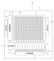
- FIG. 1 is a planar layout diagram illustrating a schematic configuration example of a solid-state imaging device according to a first embodiment of the present disclosure.
- 1 is a block diagram showing a configuration example of a solid-state imaging device according to a first embodiment of the present disclosure.
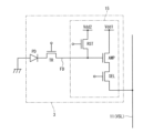
- 2 is an equivalent circuit diagram of a pixel unit of the solid-state imaging device according to the first embodiment of the present disclosure.
- FIG. 1 is a plan view (part 1) illustrating an example of a schematic structure of a solid-state imaging device according to a comparative example of the first embodiment of the present disclosure.
- FIG. 2 is a plan view (part 2) illustrating an example of a schematic structure of a solid-state imaging device according to a comparative example of the first embodiment of the present disclosure.
- FIG. 4B is a partial cross-sectional view showing an example of a schematic structure of a solid-state imaging device taken along line A-A' in FIG. 4A.
- FIG. 1 is a plan view (part 1) illustrating an example of a schematic structure of a solid-state imaging device according to a first embodiment of the present disclosure.
- FIG. 2 is a plan view (part 2) showing an example of a schematic structure of the solid-state imaging device according to the first embodiment of the present disclosure.
- 6B is a partial cross-sectional view showing an example of a schematic structure of a solid-state imaging device taken along line A-A' in FIG. 6A.
- FIG. 1A to 1C are cross-sectional views (part 1) illustrating a process procedure of a method for manufacturing a solid-state imaging device according to a first embodiment of the present disclosure.
- 5A to 5C are cross-sectional views (part 2) illustrating a process procedure of the method for manufacturing the solid-state imaging device according to the first embodiment of the present disclosure.
- 5A to 5C are cross-sectional views (part 3) illustrating a process procedure of the method for manufacturing the solid-state imaging device according to the first embodiment of the present disclosure.
- 4A to 4C are cross-sectional views showing a process procedure of the method for manufacturing the solid-state imaging device according to the first embodiment of the present disclosure (part 4).
- 5A to 5C are cross-sectional views showing a process procedure of the method for manufacturing the solid-state imaging device according to the first embodiment of the present disclosure (part 5).
- 6A to 6C are cross-sectional views showing a process procedure of the method for manufacturing the solid-state imaging device according to the first embodiment of the present disclosure;
- 7A to 7C are cross-sectional views showing a process procedure of the method for manufacturing the solid-state imaging device according to the first embodiment of the present disclosure (part 7).
- FIG. 8 is a cross-sectional view (part 8) showing a process procedure of the method for manufacturing the solid-state imaging device according to the first embodiment of the present disclosure.
- FIG. FIG. 11 is a plan view (part 1) illustrating an example of a schematic structure of a solid-state imaging device according to a second embodiment of the present disclosure, as viewed from an element formation surface.
- FIG. 13 is a plan view (part 2) illustrating an example of a schematic structure of a solid-state imaging device according to a second embodiment of the present disclosure as viewed from an element formation surface.
- FIG. 11A to 11C are cross-sectional views (part 1) illustrating a process procedure of a method for manufacturing a solid-state imaging device according to a second embodiment of the present disclosure.
- 13A to 13C are cross-sectional views (part 2) illustrating a process procedure of a method for manufacturing a solid-state imaging device according to a second embodiment of the present disclosure.
- 11A to 11C are cross-sectional views (part 3) illustrating a process procedure of a method for manufacturing a solid-state imaging device according to a second embodiment of the present disclosure.
- FIG. 11A to 11C are cross-sectional views (part 4) illustrating a process procedure of a method for manufacturing a solid-state imaging device according to a second embodiment of the present disclosure.
- 5A to 5C are cross-sectional views showing a process procedure of a method for manufacturing a solid-state imaging device according to a second embodiment of the present disclosure (part 5).
- 13 is a partial cross-sectional view showing an example of a schematic structure of a solid-state imaging device according to a third embodiment of the present disclosure.
- FIG. FIG. 11 is a partial cross-sectional view (part 1) illustrating an example of a schematic structure of a solid-state imaging device according to a fourth embodiment of the present disclosure.
- FIG. 13 is a partial cross-sectional view (part 2) illustrating an example of a schematic structure of a solid-state imaging device according to a fourth embodiment of the present disclosure.
- FIG. 13 is a partial cross-sectional view (part 1) showing an example of a schematic structure of a solid-state imaging device according to a fifth embodiment of the present disclosure.
- FIG. 13 is a partial cross-sectional view (part 2) illustrating an example of a schematic structure of a solid-state imaging device according to a fifth embodiment of the present disclosure.
- 13 is a partial cross-sectional view showing an example of a schematic structure of a solid-state imaging device according to a sixth embodiment of the present disclosure.
- FIG. 13 is a partial cross-sectional view showing an example of a schematic structure of a solid-state imaging device according to a seventh embodiment of the present disclosure.
- FIG. 13 is a partial cross-sectional view showing an example of a schematic structure of a solid-state imaging device according to an eighth embodiment of the present disclosure.
- FIG. 1 is a block diagram showing an example configuration of an imaging system as an electronic device to which the present technology is applied.
- 1 is a block diagram showing a schematic configuration example of a vehicle control system that is an example of a mobile object control system to which the technology according to the present disclosure can be applied.
- 20 is a diagram showing an example of an installation position of the imaging unit shown in FIG. 19.
- first conductivity type refers to either p-type or n-type
- second conductivity type refers to either p-type or n-type that is different from the “first conductivity type.”
- first conductivity type refers to either p-type or n-type
- second conductivity type refers to either p-type or n-type that is different from the “first conductivity type.”
- “+” or “-” attached to “n” or “p” means that the semiconductor region has a relatively high or low impurity density, respectively, compared to a semiconductor region without the "+” or “-” attached. However, even if the same "n” and "n” are attached to the same semiconductor region, this does not mean that the impurity density of each semiconductor region is strictly the same.
- CMOS Complementary Metal Oxide Semiconductor
- the solid-state imaging device is an example of a photodetection device.
- the photodetection device includes not only solid-state imaging devices but also devices that only detect light, such as distance measuring devices.
- First, the overall configuration of the solid-state imaging device 1A will be described. 1, a solid-state imaging device 1A according to an embodiment of the present technology is mainly configured with a semiconductor chip 2 having a rectangular two-dimensional planar shape when viewed in a plan view.
- the solid-state imaging device 1A is mounted on the semiconductor chip 2.
- This solid-state imaging device 1A takes in image light from a subject via an optical lens (not shown), converts the amount of incident light imaged on an imaging surface into an electrical signal on a pixel-by-pixel basis, and outputs the electrical signal as a pixel signal.
- the semiconductor chip 2 on which the solid-state imaging device 1A is mounted has a square pixel region 2A located in the center of a two-dimensional plane including mutually orthogonal X and Y directions, and a peripheral region 2B disposed outside the pixel region 2A so as to surround the pixel region 2A.
- the pixel region 2A is a light receiving surface that receives light focused by, for example, an optical lens.
- a plurality of pixels 3 are arranged in a matrix on a two-dimensional plane including the X direction and the Y direction.
- the pixels 3 are repeatedly arranged in each of the X direction and the Y direction that are mutually orthogonal within the two-dimensional plane.
- a plurality of terminal pads 14 are arranged in the peripheral region 2B.
- Each of the plurality of terminal pads 14 is arranged, for example, along four sides in a two-dimensional plane of the semiconductor chip 2.
- Each of the plurality of terminal pads 14 is an input/output terminal used when electrically connecting the semiconductor chip 2 to an external device.
- the semiconductor chip 2 includes a logic circuit 13 including a vertical drive circuit 4, a column signal processing circuit 5, a horizontal drive circuit 6, an output circuit 7, and a control circuit 8.
- the logic circuit 13 outputs an output voltage (Vout) for each pixel 3 to the outside.
- the logic circuit 13 is configured with a CMOS (Complementary MOS) circuit including, as field effect transistors, for example, a p-channel conductivity type (first conductivity type) Metal Oxide Semiconductor Field Effect Transistor (MOSFET) and an n-channel conductivity type (second conductivity type) MOSFET.
- CMOS Complementary MOS
- the vertical drive circuit 4 is composed of, for example, a shift register.
- the vertical drive circuit 4 sequentially selects the desired pixel drive lines 10, supplies pulses to the selected pixel drive lines 10 for driving the pixels 3, and drives each pixel 3 row by row. That is, the vertical drive circuit 4 sequentially selects and scans each pixel 3 in the pixel area 2A vertically row by row, and supplies pixel signals from the pixels 3 based on signal charges generated by the photoelectric conversion elements of each pixel 3 according to the amount of light received to the column signal processing circuit 5 via the vertical signal lines 11.
- the column signal processing circuit 5 is arranged, for example, for each column of pixels 3, and performs signal processing such as noise removal for each pixel column on the signals output from one row of pixels 3.
- the column signal processing circuit 5 performs signal processing such as CDS (Correlated Double Sampling) and AD (Analog-to-Digital) conversion to remove pixel-specific fixed pattern noise.
- the horizontal drive circuit 6 is composed of, for example, a shift register.
- the horizontal drive circuit 6 sequentially outputs horizontal scanning pulses to the column signal processing circuits 5, thereby selecting each of the column signal processing circuits 5 in turn, and causing each of the column signal processing circuits 5 to output a pixel signal that has been subjected to signal processing to the horizontal signal line 12.
- the output circuit 7 processes and outputs pixel signals sequentially supplied from each of the column signal processing circuits 5 through the horizontal signal line 12.
- the signal processing may include buffering, black level adjustment, column variation correction, various types of digital signal processing, etc.
- the control circuit 8 generates clock signals and control signals that serve as the basis for the operation of the vertical drive circuit 4, column signal processing circuit 5, horizontal drive circuit 6, etc., based on the vertical synchronization signal, horizontal synchronization signal, and master clock signal. The control circuit 8 then outputs the generated clock signals and control signals to the vertical drive circuit 4, column signal processing circuit 5, horizontal drive circuit 6, etc.
- ⁇ Pixels> 3 is an equivalent circuit diagram showing an example of the configuration of the pixel 3.
- the pixel 3 includes a photoelectric conversion element PD, a charge accumulation region (floating diffusion) FD that accumulates (holds) the signal charge photoelectrically converted by the photoelectric conversion element PD, and a transfer transistor TR that transfers the signal charge photoelectrically converted by the photoelectric conversion element PD to the charge accumulation region FD.
- the pixel 3 also includes a readout circuit 15 electrically connected to the charge accumulation region FD.
- the photoelectric conversion element PD generates a signal charge according to the amount of light received.
- the photoelectric conversion element PD also temporarily accumulates (holds) the generated signal charge.
- the cathode side of the photoelectric conversion element PD is electrically connected to the source region of the transfer transistor TR, and the anode side is electrically connected to a reference potential line (e.g., ground).
- a photodiode is used as the photoelectric conversion element PD.
- a drain region of the transfer transistor TR is electrically connected to the charge storage region FD.
- a gate electrode of the transfer transistor TR is electrically connected to a transfer transistor driving line of the pixel driving line 10 (see FIG. 2).
- the charge holding region FD temporarily holds (accumulates) the signal charge transferred from the photoelectric conversion element PD via the transfer transistor TR.
- the readout circuit 15 reads out the signal charge stored in the charge holding region FD and outputs a pixel signal based on the signal charge.
- the readout circuit 15 includes, but is not limited to, pixel transistors, for example, an amplification transistor AMP, a selection transistor SEL, and a reset transistor RST.
- These transistors are field-effect transistors, for example, MOSFETs with a silicon oxide (SiO2) film as the gate insulating film.
- These transistors may also be MISFETs (Metal Insulator Semiconductor FETs) with a silicon nitride (Si3N4) film or a laminated film of a silicon nitride film and a silicon oxide film as the gate insulating film.
- the source region of the amplification transistor AMP is electrically connected to the drain region of the selection transistor SEL, and the drain region is electrically connected to the power supply line Vdd1.
- the gate electrode of the amplification transistor AMP is electrically connected to the charge storage region FD and the source region of the reset transistor RST.
- the source region of the selection transistor SEL is electrically connected to the vertical signal line 11 (VSL), and the drain region is electrically connected to the source region of the amplification transistor AMP.
- the gate electrode of the selection transistor SEL is electrically connected to the selection transistor drive line of the pixel drive line 10 shown in FIG. 2.
- the source region of the reset transistor RST is electrically connected to the charge storage region FD and the gate electrode of the amplification transistor AMP, and the drain region is electrically connected to the power supply line Vdd2.
- the transfer transistor TR When the transfer transistor TR is turned on, it transfers the signal charge generated by the photoelectric conversion element PD to the charge holding region FD.
- the reset transistor RST When the reset transistor RST is turned on, it resets the potential (signal charge) of the charge holding region FD to the potential of the power supply line Vdd2.
- the selection transistor SEL controls the output timing of the pixel signal from the readout circuit 15.
- the amplification transistor AMP generates a pixel signal whose voltage corresponds to the level of the signal charge held in the charge holding region FD.
- the amplification transistor AMP constitutes a source-follower type amplifier, and outputs a pixel signal whose voltage corresponds to the level of the signal charge generated by the photoelectric conversion element PD.
- the selection transistor SEL is turned on, the amplification transistor AMP amplifies the potential of the charge holding region FD, and outputs a pixel signal corresponding to that potential to the column signal processing circuit 5 via the vertical signal line 11 (VSL).
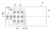
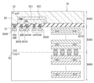
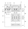
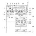
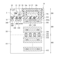
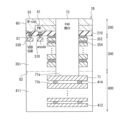
- Comparative Example 4A and 4B are plan views showing an example of a schematic structure of a solid-state imaging device B1 according to a comparative example of the first embodiment of the present disclosure, and Fig. 5A and Fig. 5B are partial cross-sectional views showing an example of a schematic structure of the solid-state imaging device B1 taken along line AA' shown in Fig. 4A and Fig. 4B.
- the solid-state imaging device B1 includes a semiconductor chip B2.
- the semiconductor chip B2 is composed of a single crystal silicon substrate of a first conductivity type, for example, p-type.
- the semiconductor chip B2 includes a well region B21 of a second conductivity type, for example, n-type, and a well region B22 of a first conductivity type, for example, p-type.
- Protection diodes B31 to B33 are disposed in the p-type well region B22.
- a power supply terminal B34 is provided in the n-type well region B21 for applying a power supply VDD to the protection diodes B31 to B33.
- the semiconductor chip B2 is provided with a terminal B35 for supplying a reference potential.
- a terminal pad B14 is provided in an area adjacent to the protection diodes B31 to B33 of the semiconductor chip B2.
- the upper surface of the terminal pad B14 is exposed through an opening B41.
- the semiconductor chip B2 includes a semiconductor layer B200 having a first surface S1 and a second surface S2 located opposite each other, a first wiring layer B300 superimposed on the first surface S1 of the semiconductor layer B200, and a second wiring layer B400 superimposed on a third surface S3, which is the surface of the first wiring layer B300 opposite the surface on the semiconductor layer B200 side.
- a laminated structure can be realized, for example, by stacking the first wiring layer B300 on the first surface S1 of the semiconductor layer B200, and superimposing and bonding the second wiring layer B400 on the third surface S3 of the first wiring layer B300.
- the second surface S2, which is one surface of the semiconductor layer B200 is sometimes called the light incident surface or back surface
- the first surface S1, which is the other surface of the semiconductor layer B200 is sometimes called the element formation surface or front surface.
- the semiconductor chip B2 has an element isolation section B210 on the first surface S1 side.
- the element isolation section B210 is an area that isolates each element including the protection diodes B31 to B33.
- a metal layer B310 connected to the anode of the protection diode B32, a metal layer B320 connected to the cathode of the protection diode B32, a metal layer B330 connected to the power supply terminal B34, and a metal layer B340 connected to the terminal B35 are formed.
- the terminal pads B14 are provided in regions adjacent to the protection diodes B31 to B33 of the semiconductor chip B2.
- the terminal pads B14 are exposed to the outside from the second surface S2 of the semiconductor chip B2 through openings B41.
- an area is required in the semiconductor chip B2 for arranging a certain number of protection diodes B31 to B33, which increases the chip area.
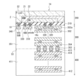
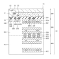
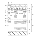
- 6A and 6B are plan views showing an example of a schematic structure of the solid-state imaging device 1A according to the first embodiment of the present disclosure
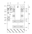
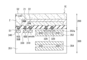
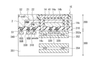
- Fig. 7A and 7B are partial cross-sectional views showing an example of a schematic structure of the solid-state imaging device 1A taken along line AA' shown in Fig. 6A and Fig. 6B.
- the semiconductor chip 2 is composed of a single crystal silicon substrate of a first conductivity type, for example, p-type.
- the semiconductor chip 2 has a well region 21 of a second conductivity type, for example, n-type, and a well region 22 of a first conductivity type, for example, p-type.
- Protection diodes 31-33 are arranged in the p-type well region 22.
- a power supply terminal 34 is provided in the n-type well region 21 for applying a power supply voltage VDD to the protection diodes 31-33.
- the semiconductor chip 2 is provided with a terminal 35 for supplying a reference potential. Note that in addition to the protection diodes 31-33, elements such as transistors that protect the transistors in the semiconductor chip 2 from ESD and PID may also be used.
- the semiconductor chip 2 is provided with an element isolation section 210 on the first surface S1 side.
- terminal pads 14 are provided in the region of the semiconductor chip 2 where the protection diodes 31 to 33 are provided.
- the upper surface of the terminal pads 14 is exposed through an opening 41 (an example of a pad opening).
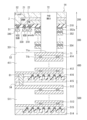
- the semiconductor chip 2 includes a semiconductor layer 200 having a first surface S1 and a second surface S2 located opposite each other, a first wiring layer 300 superimposed on the first surface S1 of the semiconductor layer 200, and a second wiring layer 400 superimposed on a third surface S3, which is the surface of the first wiring layer 300 opposite the surface on the semiconductor layer 200 side.
- a laminated structure can be realized, for example, by stacking the first wiring layer 300 on the first surface S1 of the semiconductor layer 200, and superimposing and bonding the second wiring layer 400 on the third surface S3 of the first wiring layer 300.
- the solid-state imaging device 1A is a back-illuminated imaging device (an example of a light detection device) in which the first surface S1 is the front surface and the second surface S2 is the back surface.
- the semiconductor chip 2 has an element isolation section 210 on the first surface S1 side.
- the element isolation section 210 is an area that isolates each element including the protection diodes 31 to 33.
- a metal layer 310 connected to the anode of the protection diode 32, a metal layer 320 connected to the cathode of the protection diode 32, a metal layer 330 connected to the power supply terminal 34, and a metal layer 340 connected to the terminal 35 are formed.
- the terminal pad 14 is embedded in the semiconductor layer 200, that is, it is located closer to the first surface S1 than the second surface S2 of the semiconductor layer 200, and has an upper surface 14a, a lower surface 14b opposite to the upper surface 14a, and a via 14c.
- the upper surface 14a is an exposed surface exposed to the outside through the opening 41.
- the terminal pad 14 is an input/output terminal used when electrically connecting the solid-state imaging device 1A to an external device. Therefore, the terminal pad 14 is exposed to the outside.
- the lower surface 14b of the terminal pad 14 is connected to the via 14c.
- the terminal pad 14 is made of a conductive material such as aluminum.
- a plurality of vias 14c are provided. More specifically, two vias 14c are provided.
- the vias 14c are embedded in the semiconductor layer 200 and electrically connect the terminal pad 14 to a metal layer 352 described later.
- One end of the via 14c penetrates the semiconductor layer 200 and is connected to the lower surface 14b of the terminal pad 14.
- the other end of the via 14c extends in the thickness direction of the semiconductor layer 200 through the n-type well region 21 and the p-type well region 22 that constitute the protection diodes 31 to 33 and the element isolation portion 210 into the first wiring layer 300. Then, it is connected to a metal layer 352 in the first wiring layer 300.
- the metal layer 352 to which the other end of the via 14c is connected is called the metal layer 352a to distinguish it from the other metal layers 352.
- the protection diodes 31 to 33 are located between the lower surface 14b of the terminal pad 14 and the metal layer 352a.
- the first wiring layer 300 further includes an interlayer insulating film 351, a metal layer 352 (an example of metal wiring), a first connection pad 353, and a via 354.
- the metal layer 352 and the first connection pad 353 are stacked via the interlayer insulating film 351 as shown in the figure.
- the via 354 connects the metal layers 352 to each other and connects the metal layer 352 to the first connection pad 353.
- the second wiring layer 400 includes an interlayer insulating film 411, a metal layer 412, a second connection pad 413, and a via 414.
- the metal layer 412 and the second connection pad 413 are laminated with the interlayer insulating film 411 interposed therebetween as shown in the figure.
- the via 414 connects the metal layers 412 to each other and between the metal layer 412 and the second connection pad 413.
- the second connection pad 413 is joined to the first connection pad 353.
- the terminal pad 14 is electrically connected to the metal layer 412 of the second wiring layer 400.
- FIG. 7B the second wiring layer 400 includes an interlayer insulating film 411, a metal layer 412, a second connection pad 413, and a via 414.
- the metal layer 412 and the second connection pad 413 are laminated with the interlayer insulating film 411 interposed therebetween as shown in the figure.
- the via 414 connects the metal layers 412 to each other and between the metal layer 412 and the second connection
- the second wiring layer 400 may include a logic substrate on which the logic circuit 13 is formed.
- the logic substrate includes, for example, the logic circuit 13 such as the control circuit 8 that controls the operation of each pixel 3.
- Figs. 8A to 8H are cross-sectional views showing the steps of the method for manufacturing the solid-state imaging device 1A according to the first embodiment of the present disclosure.
- the solid-state imaging device 1A is manufactured using various devices such as a film forming device (including a CVD (Chemical Vapor Deposition) device and a sputtering device), an ion implantation device, a heat treatment device, an etching device, a CMP (Chemical Mechanical Polishing) device, and a bonding device.
- a film forming device including a CVD (Chemical Vapor Deposition) device and a sputtering device
- an ion implantation device including a heat treatment device, an etching device, a CMP (Chemical Mechanical Polishing) device, and a bonding device.
- these devices are collectively referred to as manufacturing devices.
- a substrate 51 is prepared in which a semiconductor layer 200, a first wiring layer 300, and a second wiring layer 400 are stacked in that order.
- An n-type well region 21, a p-type well region 22, an element isolation portion 210, and the like are already formed in the semiconductor layer 200.
- a first connection pad 353 and a second connection pad 413 are bonded.
- the manufacturing equipment forms an opening 52 by etching on the second surface S2 of the semiconductor layer 200.
- the manufacturing equipment forms openings 53 and 54 by etching from the opening 52 to the element isolation portion 210.
- the manufacturing equipment fills the openings 52, 53, and 54 with an oxide film 55.
- the manufacturing equipment etches the oxide film 55 to form an opening 56 for forming the terminal pad 14 and its via 14c. At this time, the opening 56 penetrates the element isolation portion 210 and reaches the metal layer 320 of the first wiring layer 300.
- the manufacturing equipment patterns, for example, aluminum in the opening 56 to form the terminal pad 14.
- the manufacturing equipment fills in the areas not filled with aluminum with oxide film 57.
- the manufacturing equipment etches oxide film 57 to form openings 41 that expose upper surfaces 14a of terminal pads 14 to the outside.
- the protection diodes 31 to 33 As described above, according to the first embodiment, by arranging the protection diodes 31 to 33 between the lower surface 14b of the terminal pad 14 and the first wiring layer 300, it is not necessary to secure an area for a certain number of protection diodes 31 to 33 in the semiconductor chip 2 separately from the terminal pad 14, and this makes it possible to reduce the chip area. In addition, by providing the terminal pad 14 in the semiconductor layer 200, wire bonding can be easily performed. Note that the terminal pad 14 may have a structure in which a part of it is embedded in the semiconductor layer 200 and another part of it protrudes above the semiconductor layer 200.
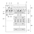
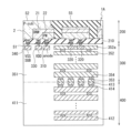
- Second Embodiment 9A and 9B are plan views showing an example of a schematic structure of a solid-state imaging device 1B according to a second embodiment of the present disclosure, as viewed from an element formation surface.
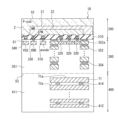
- FIGS. 10A and 10B are partial cross-sectional views showing an example of a schematic structure of the solid-state imaging device 1B cut along line BB' shown in FIGS. 9A and 9B.
- FIGS. 9A and 9B the same parts as those in FIGS. 6A and 6B are given the same reference numerals, and detailed descriptions thereof are omitted.
- FIGS. 10A and 10B the same parts as those in FIGS. 7A and 7B are given the same reference numerals, and detailed descriptions thereof are omitted.
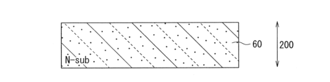
- the semiconductor chip 60 of the solid-state imaging device 1B is composed of a single crystal silicon substrate of a second conductivity type, for example, n-type.
- the semiconductor chip 60 has a well region 61 of a first conductivity type, for example, p-type.
- the semiconductor chip 60 is provided with a power supply terminal 34 for applying a power supply VDD to the protection diodes 31 to 33.
- the cathodes of the protection diodes 31 to 33 are surrounded by a plurality of vias 354 of the first wiring layer 300, which will be described later.
- a terminal pad 71 is provided in the region of the semiconductor chip 60 where the protection diodes 31 to 33 are provided.
- the upper surface 71a of the terminal pad 71 is exposed through an opening 72 (an example of a pad opening).
- the semiconductor chip 60 includes a semiconductor layer 200 having a first surface S1 and a second surface S2 located opposite each other, a first wiring layer 300 superimposed on the first surface S1 of the semiconductor layer 200, and a second wiring layer 400 superimposed on a third surface S3, which is the surface of the first wiring layer 300 opposite the surface on the semiconductor layer 200 side.
- a laminated structure can be realized, for example, by stacking the first wiring layer 300 on the first surface S1 of the semiconductor layer 200, and superimposing and bonding the second wiring layer 400 on the third surface S3 of the first wiring layer 300.
- the second surface S2, which is one surface of the semiconductor layer 200 is sometimes called the light incident surface or back surface
- the first surface S1, which is the other surface of the semiconductor layer 200 is sometimes called the element formation surface or front surface.
- the semiconductor chip 60 has an element isolation section 210 on the first surface S1 side.
- a metal layer 310 connected to the anode of the protection diode 32, a metal layer 320 connected to the cathode of the protection diode 32, and a metal layer 330 connected to the power supply terminal 34 are formed.
- the first wiring layer 300 further includes an interlayer insulating film 351, a metal layer 352 (an example of metal wiring), and a via 354.
- the metal layer 352 is stacked with the interlayer insulating film 351 interposed therebetween as shown.
- the via 354 connects the metal layers 352 to each other.
- the second wiring layer 400 includes a terminal pad 71, an interlayer insulating film 411, a metal layer 412, and a via 414.
- the terminal pad 71 and the metal layer 412 are stacked with the interlayer insulating film 411 interposed therebetween as shown.
- the via 414 connects the metal layers 412 to each other and between the metal layer 412 and the terminal pad 71. This electrically connects the terminal pad 71 to the metal layer 412 of the second wiring layer 400.
- the second wiring layer 400 may include a logic substrate that forms a logic circuit.
- the logic substrate includes, for example, a pixel control circuit that controls the operation of each pixel 3, and a front-end circuit that realizes quenching and recharging of each pixel 3.
- the terminal pad 71 is provided as a metal layer 412 in the second wiring layer 400, and has an upper surface 71a and a lower surface 71b, which is the surface opposite to the upper surface 71a.
- the upper surface 71a is an exposed surface that is exposed to the outside through the opening 72.
- the terminal pad 71 is an input/output terminal used when electrically connecting the solid-state imaging device 1B to an external device. Therefore, the terminal pad 71 is exposed to the outside.
- the lower surface 71b of the terminal pad 71 is connected to the via 414.
- the via 414 electrically connects the terminal pad 71 to the metal layer 412.
- an opening 72 is formed from the second surface S2 of the semiconductor layer 200, i.e., the light incident surface, to the terminal pad 71 of the second wiring layer 400.
- the protection diodes 31 to 33 are disposed at the formation position of this opening 72. After the formation of this opening 72, the protection diodes 31 to 33 disappear.
- Figs. 11A to 11E are cross-sectional views showing the steps of the method for manufacturing the solid-state imaging device 1B according to the second embodiment of the present disclosure.
- the solid-state imaging device 1B is manufactured using various devices such as a film forming device (including a CVD (Chemical Vapor Deposition) device and a sputtering device), an ion implantation device, a heat treatment device, an etching device, a CMP (Chemical Mechanical Polishing) device, and a bonding device.
- a film forming device including a CVD (Chemical Vapor Deposition) device and a sputtering device
- an ion implantation device including a heat treatment device, an etching device, a CMP (Chemical Mechanical Polishing) device, and a bonding device.
- these devices are collectively referred to as manufacturing devices.
- a semiconductor chip 60 including only a semiconductor layer 200 is prepared.
- the manufacturing equipment forms a p-type well region 61 and an element isolation portion 210 in the semiconductor layer 200 of the semiconductor chip 60.
- the manufacturing equipment laminates the first wiring layer 300 on the surface of the semiconductor layer 200 where the element isolation portion 210 is formed.
- an interlayer insulating film 351, a metal layer 352, and a via 354 are formed in the first wiring layer 300.
- the plasma charge generated may cause PID (Process Induced Damage) that causes gate failure of the transistor.
- a protection diode 32 is disposed in the arrangement area of the terminal pad 71, and, for example, a metal layer 310 connected to the anode of the protection diode 32, a metal layer 320 connected to the cathode of the protection diode 32, and a metal layer 330 connected to the power supply terminal 34 are formed in the first wiring layer 300.
- the manufacturing equipment laminates the second wiring layer 400 on the upper surface of the support substrate 73, inverts the semiconductor chip 60 from the state shown in FIG. 11C, and bonds the first connection pad 353 of the first wiring layer 300 to the second connection pad 413 of the second wiring layer 400.
- the manufacturing equipment forms an opening 72 from the second surface S2 of the semiconductor layer 200, i.e., the light incident surface, to the terminal pad 71 of the second wiring layer 400, and exposes the upper surface 71a of the terminal pad 71 to the outside. With the formation of this opening 72, the protection diodes 31 to 33 arranged in the semiconductor layer 200 disappear.
- the protection diodes 31 to 33 are disposed at the formation position of the opening 72. This makes it possible to protect other elements in the semiconductor layer 200 from ESD, PID, and the like until the opening 72 is formed, and also makes it unnecessary to secure an area for a certain number of protection diodes 31 to 33 in the semiconductor layer 200 separate from the terminal pad 71, thereby enabling a reduction in the chip area.
- Third Embodiment 12 is a partial cross-sectional view showing an example of a schematic structure of a solid-state imaging device 1C according to a third embodiment of the present disclosure.
- FIG. 12 the same parts as those in FIG. 7B and FIG. 10A are denoted by the same reference numerals, and detailed description thereof will be omitted.
- the semiconductor chip 60 of the solid-state imaging device 1C is composed of a single crystal silicon substrate of a second conductivity type, for example, n-type.
- the semiconductor chip 60 has a well region 61 of a first conductivity type, for example, p-type.
- the semiconductor chip 60 is provided with a power supply terminal 34 for applying a power supply VDD to the protection diodes 31 to 33.
- the terminal pad 14 is embedded in the semiconductor layer 200, that is, it is located closer to the first surface S1 than the second surface S2 of the semiconductor layer 200, and has an upper surface 14a, a lower surface 14b which is the surface opposite to the upper surface 14a, and a via 14c.
- the upper surface 14a is an exposed surface exposed to the outside through the opening 41.
- the terminal pad 14 is an input/output terminal used when electrically connecting the solid-state imaging device 1A to an external device. Therefore, the terminal pad 14 is exposed to the outside.
- the lower surface 14b of the terminal pad 14 is connected to the via 14c.
- a plurality of vias 14c are provided. More specifically, two vias 14c are provided.
- the vias 14c are embedded in the semiconductor layer 200 and electrically connect the terminal pad 14 and the metal layer 352.
- One end of the via 14c penetrates the semiconductor layer 200 and is connected to the lower surface 14b of the terminal pad 14.
- the other end of the via 14c penetrates the n-type well region 21 and the p-type well region 22 that constitute the protection diodes 31 to 33, and the element isolation portion 210 in the thickness direction of the semiconductor layer 200, and extends into the first wiring layer 300. Then, it is connected to the metal layer 352 in the first wiring layer 300.
- the metal layer 352 to which the other end of the via 14c is connected is called the metal layer 352a to distinguish it from the other metal layers 352.
- the protection diodes 31 to 33 are located between the lower surface 14b of the terminal pad 14 and the metal layer 352a.
- the third embodiment also provides the same effects as the first embodiment.
- the semiconductor chip 2 of the solid-state imaging device 1D is composed of a single crystal silicon substrate of a first conductivity type, for example, p-type.
- the semiconductor chip 2 has a well region 21 of a second conductivity type, for example, n-type, and a well region 22 of the first conductivity type, for example, p-type.
- Protection diodes 31 to 33 are disposed in the p-type well region 22.
- a power supply terminal 34 is provided in the n-type well region 21 for applying a power supply VDD to the protection diodes 31 to 33.
- the semiconductor chip 2 is provided with a terminal 35 for supplying a reference potential.
- a metal layer 310 connected to the anode of the protection diode 32, a metal layer 320 connected to the cathode of the protection diode 32, a metal layer 330 connected to the power supply terminal 34, and a metal layer 340 connected to the terminal 35 are formed.
- the terminal pad 71 is provided as a metal layer 412 in the second wiring layer 400, and has an upper surface 71a and a lower surface 71b, which is the surface opposite to the upper surface 71a.
- the upper surface 71a is an exposed surface that is exposed to the outside through an opening 72.
- the terminal pad 71 is an input/output terminal used when electrically connecting the solid-state imaging device 1B to an external device. Therefore, the terminal pad 71 is exposed to the outside.
- the lower surface 71b of the terminal pad 71 is connected to a via 414.
- the via 414 electrically connects the terminal pad 71 to the metal layer 412.
- an opening 72 is formed from the second surface S2 of the semiconductor layer 200, i.e., the light incident surface, to the terminal pad 71 of the second wiring layer 400.
- the protection diodes 31 to 33 are disposed at the formation position of this opening 72. After the formation of this opening 72, the protection diodes 31 to 33 disappear.
- the fourth embodiment also provides the same effects as the second embodiment.
- Fifth embodiment 14A and 14B are partial cross-sectional views showing an example of a schematic structure of a solid-state imaging device 1E according to a fifth embodiment of the present disclosure.
- Fig. 14A and Fig. 14B the same parts as those in Fig. 7A and Fig. 7B are denoted by the same reference numerals and detailed description thereof will be omitted.
- the semiconductor chip 2 of the solid-state imaging device 1E includes a semiconductor layer 200 having a first surface S1 and a second surface S2 located on opposite sides, and a first wiring layer 300 superimposed on the first surface S1 of the semiconductor layer 200.
- the terminal pad 14 is embedded in the semiconductor layer 200, that is, it is located closer to the first surface S1 than the second surface S2 of the semiconductor layer 200, and has an upper surface 14a, a lower surface 14b which is the surface opposite to the upper surface 14a, and a via 14c.
- the fifth embodiment also provides the same effects as the first embodiment.
- Sixth embodiment 15 is a partial cross-sectional view showing an example of a schematic structure of a solid-state imaging device 1F according to a sixth embodiment of the present disclosure.
- the same parts as those in FIG. 7B are denoted by the same reference numerals, and detailed description thereof will be omitted.
- the semiconductor chip 2 includes a semiconductor layer 200 having a first surface S1 and a second surface S2 located opposite to each other, a first wiring layer 300 superimposed on the first surface S1 of the semiconductor layer 200, a second wiring layer 400 superimposed on a third surface S3, which is the surface of the first wiring layer 300 opposite to the surface on the semiconductor layer 200 side, and a third wiring layer 500 superimposed on a fourth surface S4, which is the surface of the second wiring layer 400 opposite to the third surface S3.
- Such a laminated structure can be realized, for example, by stacking the first wiring layer 300 on the first surface S1 of the semiconductor layer 200, superimposing and bonding the second wiring layer 400 to the third surface S3 of the first wiring layer 300, and superimposing and bonding the third wiring layer 500 to the fourth surface S4 of the second wiring layer 400.
- the third wiring layer 500 includes an interlayer insulating film 511, a metal layer 512, and a via 513.
- the metal layer 512 is laminated via the interlayer insulating film 511 as shown in the figure.
- the via 513 connects the metal layers 512 to each other.
- the metal layer 512 is joined to the metal layer 412 of the second wiring layer 400 by a through via 81 made of a conductive material. This electrically connects the terminal pad 14 to the metal layer 512 of the third wiring layer 500.
- the terminal pad 14, the first connection pad 353, and the second connection pad 413 overlap in the thickness direction of the semiconductor chip 2, but the terminal pad 14 and the through via 81 do not overlap in the thickness direction of the semiconductor chip 2.
- the second wiring layer 400 has a first substrate 415.
- the first substrate 415 is, for example, a second-stage pixel substrate or a logic substrate forming a logic circuit such as the control circuit 8.
- the first substrate 415 is located on the fourth surface S4 side and is made of a semiconductor substrate of a first conductivity type, for example, a p-type.
- the first substrate 415 is provided with an element isolation portion 416 that isolates a plurality of transistors and the like from other elements. Furthermore, the first substrate 415 is electrically connected to the metal layer 412 by a via 414.
- the third wiring layer 500 has a second substrate 514 on which a logic circuit such as the column signal processing circuit 5 is formed.
- the second substrate 514 is located on the surface opposite to the fourth surface and is made of a semiconductor substrate of a first conductivity type, for example, a p-type.
- the second substrate 514 is provided with an element isolation section 515 that isolates a plurality of transistors from other elements. Furthermore, the second substrate 514 is electrically connected to the metal layer 512 by a via 513.
- the sixth embodiment can provide the same effects as the first embodiment. Furthermore, according to the sixth embodiment, various circuits such as the column signal processing circuit 5 and the control circuit 8 constituting the logic circuit 13 can be arranged in the thickness direction of the semiconductor chip 2, so that the area of the entire solid-state imaging device 1F can be reduced.
- Seventh embodiment 16 is a partial cross-sectional view showing an example of a schematic structure of a solid-state imaging device 1G according to a seventh embodiment of the present disclosure.
- Fig. 16 the same parts as those in Fig. 15 are denoted by the same reference numerals and detailed description thereof will be omitted.
- the third wiring layer 500 includes an interlayer insulating film 511, a metal layer 512, a via 513, and a third connection pad 516.
- the metal layer 512 and the third connection pad 516 are stacked with the interlayer insulating film 511 interposed therebetween as shown.
- the via 513 connects the metal layers 512 to each other and between the metal layer 512 and the third connection pad 516.
- the third connection pad 516 is joined to the second connection pad 413. As a result, the terminal pad 14 is electrically connected to the metal layer 512 of the third wiring layer 500.
- the first substrate 415 is located on the third surface S3 side.
- the through via 81 joins the metal layer 352 of the first wiring layer 300 and the metal layer 412 of the second wiring layer 400. At this time, the through via 81 penetrates the first substrate 415.
- the seventh embodiment can provide the same effects as the sixth embodiment.
- FIG. 17 is a partial cross-sectional view showing an example of a schematic structure of a solid-state imaging device 1H according to an eighth embodiment of the present disclosure.
- Fig. 17 the same parts as those in Fig. 13B and Fig. 15 are denoted by the same reference numerals and detailed description thereof will be omitted.
- the terminal pad 71 is provided as a metal layer 412 in the second wiring layer 400, and has an upper surface 71a and a lower surface 71b, which is the surface opposite to the upper surface 71a.
- the upper surface 71a is an exposed surface exposed to the outside through an opening 72.
- the metal layer 512 of the third wiring layer 500 is joined to the metal layer 412 of the second wiring layer 400 by a through via 81 of a conductive material. This electrically connects the terminal pad 71 to the metal layer 512 of the third wiring layer 500.
- the eighth embodiment can provide the same effects as those of the second embodiment. Furthermore, according to the eighth embodiment, various circuits such as the column signal processing circuit 5 and the control circuit 8 constituting the logic circuit 13 can be arranged in the thickness direction of the semiconductor chip 2, so that the area of the entire solid-state imaging device 1H can be reduced.
- FIG. 18 is a block diagram showing an example configuration of an imaging system as an electronic device to which the present technology is applied.
- the imaging system 2201 shown in FIG. 18 is configured with an optical system 2202, a shutter device 2203, a solid-state imaging element 2204 as a solid-state imaging device, a control circuit 2205, a signal processing circuit 2206, a monitor 2207, and two memories 2208, and is capable of capturing still images and moving images.
- the optical system 2202 is configured to have one or more lenses, and guides light from a subject (incident light) to the solid-state image sensor 2204 , forming an image on the light receiving surface of the solid-state image sensor 2204 .
- the shutter device 2203 is disposed between the optical system 2202 and the solid-state image sensor 2204 , and controls the light irradiation period and light blocking period for the solid-state image sensor 2204 under the control of a control circuit 2205 .
- the solid-state imaging element 2204 is configured by a package including the above-mentioned solid-state imaging element.
- the solid-state imaging element 2204 accumulates signal charge for a certain period of time according to the light that is imaged on the light receiving surface via the optical system 2202 and the shutter device 2203.
- the signal charge accumulated in the solid-state imaging element 2204 is transferred according to a drive signal (timing signal) supplied from the control circuit 2205.
- the control circuit 2205 drives the solid-state imaging element 2204 and the shutter device 2203 by outputting a drive signal that controls the transfer operation of the solid-state imaging element 2204 and the shutter operation of the shutter device 2203.
- the signal processing circuit 2206 performs various signal processing on the signal charges output from the solid-state imaging element 2204.
- An image (image data) obtained by performing the signal processing by the signal processing circuit 2206 is supplied to a monitor 2207 and displayed, or is supplied to a memory 2208 and stored (recorded).
- the solid-state imaging devices 1A to 1H can be applied in place of the solid-state imaging element 2204 described above.
- the technology according to the present disclosure can be applied to various products.
- the technology according to the present disclosure may be realized as a device mounted on any type of moving body such as an automobile, an electric vehicle, a hybrid electric vehicle, a motorcycle, a bicycle, a personal mobility device, an airplane, a drone, a ship, or a robot.
- FIG. 19 is a block diagram showing a schematic configuration example of a vehicle control system, which is an example of a mobile object control system to which the technology according to the present disclosure can be applied.
- the vehicle control system 12000 includes a plurality of electronic control units connected via a communication network 12001.
- the vehicle control system 12000 includes a drive system control unit 12010, a body system control unit 12020, an outside-vehicle information detection unit 12030, an inside-vehicle information detection unit 12040, and an integrated control unit 12050.
- a microcomputer 12051, an audio/video output unit 12052, and an in-vehicle network I/F (interface) 12053 are illustrated as functional configurations of the integrated control unit 12050.
- the drive system control unit 12010 controls the operation of devices related to the drive system of the vehicle according to various programs.
- the drive system control unit 12010 functions as a control device for a drive force generating device for generating the drive force of the vehicle, such as an internal combustion engine or a drive motor, a drive force transmission mechanism for transmitting the drive force to the wheels, a steering mechanism for adjusting the steering angle of the vehicle, and a braking device for generating a braking force for the vehicle.
- the body system control unit 12020 controls the operation of various devices installed in the vehicle body according to various programs.
- the body system control unit 12020 functions as a control device for a keyless entry system, a smart key system, a power window device, or various lamps such as headlamps, tail lamps, brake lamps, turn signals, and fog lamps.
- radio waves or signals from various switches transmitted from a portable device that replaces a key can be input to the body system control unit 12020.
- the body system control unit 12020 accepts the input of these radio waves or signals and controls the vehicle's door lock device, power window device, lamps, etc.
- the outside-vehicle information detection unit 12030 detects information outside the vehicle equipped with the vehicle control system 12000.
- the image capturing unit 12031 is connected to the outside-vehicle information detection unit 12030.
- the outside-vehicle information detection unit 12030 causes the image capturing unit 12031 to capture images outside the vehicle, and receives the captured images.
- the outside-vehicle information detection unit 12030 may perform object detection processing or distance detection processing for people, cars, obstacles, signs, or characters on the road surface, based on the received images.
- the imaging unit 12031 is an optical sensor that receives light and outputs an electrical signal according to the amount of light received.
- the imaging unit 12031 can output the electrical signal as an image, or as distance measurement information.
- the light received by the imaging unit 12031 may be visible light, or may be invisible light such as infrared light.
- the microcomputer 12051 can calculate the control target values of the driving force generating device, steering mechanism, or braking device based on the information inside and outside the vehicle acquired by the outside vehicle information detection unit 12030 or the inside vehicle information detection unit 12040, and output a control command to the drive system control unit 12010.
- the microcomputer 12051 can perform cooperative control aimed at realizing the functions of an ADAS (Advanced Driver Assistance System), including avoiding or mitigating vehicle collisions, following the vehicle based on the distance between vehicles, maintaining vehicle speed, vehicle collision warning, or vehicle lane departure warning.
- ADAS Advanced Driver Assistance System
- the microcomputer 12051 can also perform cooperative control for the purpose of autonomous driving, which allows the vehicle to travel autonomously without relying on the driver's operation, by controlling the driving force generating device, steering mechanism, braking device, etc. based on information about the surroundings of the vehicle acquired by the outside vehicle information detection unit 12030 or the inside vehicle information detection unit 12040.
- the microcomputer 12051 can also output control commands to the body system control unit 12020 based on information outside the vehicle acquired by the outside-vehicle information detection unit 12030. For example, the microcomputer 12051 can control the headlamps according to the position of a preceding vehicle or an oncoming vehicle detected by the outside-vehicle information detection unit 12030, and perform cooperative control aimed at preventing glare, such as switching from high beams to low beams.
- the audio/image output unit 12052 transmits at least one output signal of audio and image to an output device capable of visually or audibly notifying the occupants of the vehicle or the outside of the vehicle of information.
- an audio speaker 12061, a display unit 12062, and an instrument panel 12063 are exemplified as output devices.
- the display unit 12062 may include, for example, at least one of an on-board display and a head-up display.
- FIG. 20 is a diagram showing an example of the installation position of the imaging unit 12031.
- a vehicle 12100 has imaging units 12101, 12102, 12103, 12104, and 12105 as an imaging unit 12031.
- the imaging units 12101, 12102, 12103, 12104, and 12105 are provided, for example, at the front nose, side mirrors, rear bumper, back door, and the top of the windshield inside the vehicle cabin of the vehicle 12100.
- the imaging unit 12101 provided at the front nose and the imaging unit 12105 provided at the top of the windshield inside the vehicle cabin mainly acquire images of the front of the vehicle 12100.
- the imaging units 12102 and 12103 provided at the side mirrors mainly acquire images of the sides of the vehicle 12100.
- the imaging unit 12104 provided at the rear bumper or back door mainly acquires images of the rear of the vehicle 12100.
- the images of the front acquired by the imaging units 12101 and 12105 are mainly used to detect preceding vehicles, pedestrians, obstacles, traffic lights, traffic signs, lanes, etc.
- FIG. 20 shows an example of the imaging ranges of the imaging units 12101 to 12104.
- Imaging range 12111 indicates the imaging range of the imaging unit 12101 provided on the front nose
- imaging ranges 12112 and 12113 indicate the imaging ranges of the imaging units 12102 and 12103 provided on the side mirrors, respectively
- imaging range 12114 indicates the imaging range of the imaging unit 12104 provided on the rear bumper or back door.
- an overhead image of the vehicle 12100 viewed from above is obtained by superimposing the image data captured by the imaging units 12101 to 12104.
- At least one of the imaging units 12101 to 12104 may have a function of acquiring distance information.
- at least one of the imaging units 12101 to 12104 may be a stereo camera consisting of multiple imaging elements, or an imaging element having pixels for phase difference detection.
- the microcomputer 12051 can obtain the distance to each solid object within the imaging ranges 12111 to 12114 and the change in this distance over time (relative speed with respect to the vehicle 12100) based on the distance information obtained from the imaging units 12101 to 12104, and can extract as a preceding vehicle, in particular, the closest solid object on the path of the vehicle 12100 that is traveling in approximately the same direction as the vehicle 12100 at a predetermined speed (e.g., 0 km/h or faster). Furthermore, the microcomputer 12051 can set the inter-vehicle distance that should be maintained in advance in front of the preceding vehicle, and perform automatic braking control (including follow-up stop control) and automatic acceleration control (including follow-up start control). In this way, cooperative control can be performed for the purpose of automatic driving, which runs autonomously without relying on the driver's operation.
- automatic braking control including follow-up stop control
- automatic acceleration control including follow-up start control
- the microcomputer 12051 classifies and extracts three-dimensional object data on three-dimensional objects, such as two-wheeled vehicles, ordinary vehicles, large vehicles, pedestrians, utility poles, and other three-dimensional objects, based on the distance information obtained from the imaging units 12101 to 12104, and can use the data to automatically avoid obstacles.
- the microcomputer 12051 distinguishes obstacles around the vehicle 12100 into obstacles that are visible to the driver of the vehicle 12100 and obstacles that are difficult to see.
- the microcomputer 12051 determines the collision risk, which indicates the risk of collision with each obstacle, and when the collision risk is equal to or exceeds a set value and there is a possibility of a collision, it can provide driving assistance for collision avoidance by outputting an alarm to the driver via the audio speaker 12061 or the display unit 12062, or by forcibly decelerating or steering to avoid a collision via the drive system control unit 12010.
- At least one of the imaging units 12101 to 12104 may be an infrared camera that detects infrared rays.
- the microcomputer 12051 can recognize a pedestrian by determining whether or not a pedestrian is present in the captured image of the imaging units 12101 to 12104. The recognition of such a pedestrian is performed, for example, by a procedure of extracting feature points in the captured image of the imaging units 12101 to 12104 as infrared cameras, and a procedure of performing pattern matching processing on a series of feature points that indicate the contour of an object to determine whether or not it is a pedestrian.
- the audio/image output unit 12052 controls the display unit 12062 to superimpose a rectangular contour line for emphasis on the recognized pedestrian.
- the audio/image output unit 12052 may also control the display unit 12062 to display an icon or the like indicating a pedestrian at a desired position.
- the present disclosure can also be configured as follows. (1) a semiconductor layer having a photoelectric conversion portion, one surface of which is a light incidence surface and the other surface of which is an element formation surface; a wiring layer laminated on the element formation surface of the semiconductor layer; a terminal pad at least a part of which is located in the semiconductor layer and which is connected to a metal wiring of the wiring layer; a light detection device comprising an element disposed between the terminal pad and the wiring layer. (2) The photodetector according to claim 1, wherein the element is a protection diode for protecting other elements disposed in the semiconductor layer.
- the wiring layers include a first wiring layer laminated on an element forming surface of the semiconductor layer; a second wiring layer laminated on a surface of the first wiring layer opposite to a surface of the first wiring layer on the semiconductor layer side;
- the wiring layers include a first wiring layer laminated on an element forming surface of the semiconductor layer; a second wiring layer laminated on a surface of the first wiring layer opposite to a surface of the first wiring layer on the semiconductor layer side; a third wiring layer laminated on a surface of the second wiring layer opposite to a surface of the second wiring layer on the first wiring layer side;
- a photodetection device comprising: a first pad opening formed on the first substrate; a second pad opening formed on the first substrate; (9) The photodetector according to claim 8, wherein the element is a protection diode for protecting other elements disposed in the semiconductor layer.
- the photodetector device according to claim 12, wherein the terminal pad is located in the second wiring layer.
- the wiring layers include a first wiring layer laminated on an element forming surface of the semiconductor layer; a second wiring layer laminated on a surface of the first wiring layer opposite to a surface of the first wiring layer on the semiconductor layer side; a third wiring layer laminated on a surface of the second wiring layer opposite to a surface of the second wiring layer on the first wiring layer side;
- the photodetector device wherein the terminal pad is located in the second wiring layer.
- a semiconductor layer having a photoelectric conversion portion one surface of which is a light incidence surface and the other surface of which is an element formation surface; a wiring layer laminated on the element formation surface of the semiconductor layer; a terminal pad at least a part of which is located in the semiconductor layer and which is connected to a metal wiring of the wiring layer; an element disposed between the terminal pad and the wiring layer;
- An electronic device comprising a photodetector, the photodetector
- a method for manufacturing a photodetector comprising: preparing a semiconductor chip having a photoelectric conversion portion, one surface of a semiconductor layer being a light incident surface and the other surface being an element formation surface, and stacking a wiring layer on the element formation surface of the semiconductor layer; forming a terminal pad in the semiconductor layer that is connected to metal wiring of the wiring layer; and arranging an element between the terminal pad and the wiring layer.
- a semiconductor chip is prepared by laminating a wiring layer on an element formation surface of a semiconductor layer having a photoelectric conversion unit, one surface of the semiconductor layer being a light incidence surface and the other surface being an element formation surface; forming a terminal pad connected to a metal wiring of the wiring layer on the wiring layer side of the element formation surface of the semiconductor layer; forming a pad opening extending from the light incident surface of the semiconductor layer to the terminal pad and exposing the terminal pad from the light incident surface;
- a method for manufacturing a photodetector comprising: arranging an element at a position where the pad opening is to be formed before the pad opening is formed.
Landscapes
- Solid State Image Pick-Up Elements (AREA)
- Internal Circuitry In Semiconductor Integrated Circuit Devices (AREA)
Abstract
チップ面積を縮小化することが可能な光検出装置を提供する。光検出装置は、半導体層と、配線層と、端子パッドと、素子とを備える。半導体層は、光電変換部を有し、一方の面が光入射面であり他方の面が素子形成面である。配線層は、半導体層の素子形成面に積層される。端子パッドは、半導体層に少なくとも一部が位置し、配線層の金属配線と接続される。素子は、端子パッドと配線層との間に配置される。
Description
本開示に係る技術(本技術)は、光検出装置、光検出装置を備えた電子機器及び光検出装置の製造方法に関する。
固体撮像装置において、チップ内にESD(Electrostatic Discharge)やPID(Process Induced Damage)等から半導体素子を守るための保護素子が、通常各端子パッドにそれぞれ対応して一定数配置されている。特許文献1には、端子パッドの下に保護トランジスタのエミッタ領域が電気的に連結される構造が開示されている。
固体撮像装置においては、チップサイズの縮小が望まれている。しかし、保護素子は、チップ内に一定数必要とされるため、チップ面積が増大してしまう。
本開示はこのような事情に鑑みてなされたもので、チップ面積を縮小化することが可能な光検出装置、電子機器及び光検出装置の製造方法を提供することを目的とする。
本開示の一態様は、光電変換部を有し、一方の面が光入射面であり他方の面が素子形成面である半導体層と、前記半導体層の前記素子形成面に積層される配線層と、前記半導体層に少なくとも一部が位置し、前記配線層の金属配線と接続される端子パッドと、前記端子パッドと前記配線層との間に配置される素子とを備える光検出装置である。
本開示の他の態様は、光電変換部を有し、一方の面が光入射面であり他方の面が素子形成面である半導体層と、前記半導体層の前記素子形成面に積層される配線層と、前記半導体層の前記素子形成面より前記配線層側に位置し、前記配線層の金属配線と接続される端子パッドと、前記半導体層の前記光入射面から前記端子パッドに至り形成され、前記端子パッドを前記光入射面から露出するパッド開口部と、を備え、前記パッド開口部が形成される前に、前記パッド開口部の形成位置に素子を配置する、光検出装置である。
また、本開示の他の態様は、光電変換部を有し、一方の面が光入射面であり他方の面が素子形成面である半導体層と、前記半導体層の前記素子形成面に積層される配線層と、前記半導体層に少なくとも一部が位置し、前記配線層の金属配線に接続される端子パッドと、前記端子パッドと前記配線層との間に配置される素子と、を備える光検出装置を備えた、電子機器である。
また、本開示の他の態様は、光電変換部を有し、一方の面が光入射面であり他方の面が素子形成面である半導体層と、前記半導体層の前記素子形成面に積層される配線層と、前記半導体層の前記素子形成面より前記配線層側に位置し、前記配線層の金属配線に接続される端子パッドと、前記半導体層の前記光入射面から前記端子パッドに至り形成され、前記端子パッドを前記光入射面から露出するパッド開口部と、を備え、前記パッド開口部が形成される前に、前記パッド開口部の形成位置に素子を配置する、光検出装置を備えた、電子機器である。
また、本開示の他の態様は、光電変換部を有し、一方の面が光入射面であり他方の面が素子形成面である半導体層の前記素子形成面に配線層を積層した半導体チップを用意することと、前記半導体層内に、上面を外部に露出する端子パッドを形成することと、前記半導体層内に配置される素子が前記端子パッドの下面と前記配線層との間に位置するように、前記端子パッドの下面と前記配線層の金属配線とをビアにより接続することと、を備える、光検出装置の製造方法である。
さらに、本開示の他の態様は、光電変換部を有し、一方の面が光入射面であり他方の面が素子形成面である半導体層の前記素子形成面に配線層を積層した半導体チップを用意することと、前記半導体層の前記素子形成面より前記配線層側に、前記配線層の金属配線に接続される端子パッドを形成することと、前記半導体層の前記光入射面から前記端子パッドに至り、前記端子パッドを前記光入射面から露出するパッド開口部を形成することと、を備え、前記パッド開口部を形成する前に、前記パッド開口部の形成位置に素子を配置する、光検出装置の製造方法である。
以下において、図面を参照して本開示の実施形態を説明する。以下の説明で参照する図面の記載において、同一又は類似の部分には同一又は類似の符号を付し、重複する説明を省略する。但し、図面は模式的なものであり、厚みと平面寸法との関係、各装置や各部材の厚みの比率等は現実のものと異なることに留意すべきである。したがって、具体的な厚みや寸法は以下の説明を参酌して判定すべきものである。また、図面相互間においても互いの寸法の関係や比率が異なる部分が含まれていることは勿論である。
本明細書において、「第1導電型」はp型又はn型の一方であり、「第2導電型」はp型又はn型のうちの「第1導電型」とは異なる一方を意味する。また、「n」や「p」に付す「+」や「-」は、「+」及び「-」が付記されていない半導体領域に比して、それぞれ相対的に不純物密度が高い又は低い半導体領域であることを意味する。但し、同じ「n」と「n」とが付された半導体領域であっても、それぞれの半導体領域の不純物密度が厳密に同じであることを意味するものではない。
また、以下の説明における上下等の方向の定義は、単に説明の便宜上の定義であって、本開示の技術的思想を限定するものではない。例えば、対象を90°回転して観察すれば上下は左右に変換して読まれ、180°回転して観察すれば上下は反転して読まれることは勿論である。
なお、本明細書中に記載される効果はあくまで例示であって限定されるものでは無く、また他の効果があってもよい。
なお、本明細書中に記載される効果はあくまで例示であって限定されるものでは無く、また他の効果があってもよい。
<第1の実施形態>
この一実施形態では、裏面照射型のCMOS(Complementary Metal Oxide Semiconductor)イメージセンサである固体撮像装置に本技術を適用した一例について説明する。固体撮像装置は、光検出装置の一例である。光検出装置は、固体撮像装置の他に、測距デバイス等の光を検出するのみのデバイスも含む。
(固体撮像装置の全体構成)
まず、固体撮像装置1Aの全体構成について説明する。
図1に示すように、本技術の一実施形態に係る固体撮像装置1Aは、平面視したときの二次元平面形状が方形状の半導体チップ2を主体に構成されている。換言すれば、固体撮像装置1Aは、半導体チップ2に搭載されている。この固体撮像装置1Aは、光学レンズ(図示せず)を介して被写体からの像光を取り込み、撮像面上に結像された入射光の光量を画素単位で電気信号に変換して画素信号として出力する。
この一実施形態では、裏面照射型のCMOS(Complementary Metal Oxide Semiconductor)イメージセンサである固体撮像装置に本技術を適用した一例について説明する。固体撮像装置は、光検出装置の一例である。光検出装置は、固体撮像装置の他に、測距デバイス等の光を検出するのみのデバイスも含む。
(固体撮像装置の全体構成)
まず、固体撮像装置1Aの全体構成について説明する。
図1に示すように、本技術の一実施形態に係る固体撮像装置1Aは、平面視したときの二次元平面形状が方形状の半導体チップ2を主体に構成されている。換言すれば、固体撮像装置1Aは、半導体チップ2に搭載されている。この固体撮像装置1Aは、光学レンズ(図示せず)を介して被写体からの像光を取り込み、撮像面上に結像された入射光の光量を画素単位で電気信号に変換して画素信号として出力する。
図1に示すように、固体撮像装置1Aが搭載された半導体チップ2は、互いに直交するX方向及びY方向を含む二次元平面において、中央部に設けられた方形状の画素領域2Aと、この画素領域2Aの外側に画素領域2Aを囲むようにして配置された周辺領域2Bとを備えている。
画素領域2Aは、例えば光学レンズにより集光される光を受光する受光面である。そして、画素領域2Aには、X方向及びY方向を含む二次元平面において複数の画素3が行列状に配置されている。換言すれば、画素3は、二次元平面内で互いに直交するX方向及びY方向のそれぞれの方向に繰り返し配置されている。
図1に示すように、周辺領域2Bには、複数の端子パッド14が配置されている。複数の端子パッド14の各々は、例えば、半導体チップ2の二次元平面における4つの辺に沿って配列されている。複数の端子パッド14の各々は、半導体チップ2を外部装置と電気的に接続する際に用いられる入出力端子である。
<ロジック回路>
図2に示すように、半導体チップ2は、垂直駆動回路4、カラム信号処理回路5、水平駆動回路6、出力回路7及び制御回路8などを含むロジック回路13を備えている。ロジック回路13は、画素3毎の出力電圧(Vout)を外部に出力する。ロジック回路13は、電界効果トランジスタとして、例えば、pチャネル導電型(第1の導電型)のMOSFET(Metal Oxide Semiconductor Field Effect Transistor)及びnチャネル導電型(第2の導電型)のMOSFETを含むCMOS(Complementary MOS)回路で構成されている。
図2に示すように、半導体チップ2は、垂直駆動回路4、カラム信号処理回路5、水平駆動回路6、出力回路7及び制御回路8などを含むロジック回路13を備えている。ロジック回路13は、画素3毎の出力電圧(Vout)を外部に出力する。ロジック回路13は、電界効果トランジスタとして、例えば、pチャネル導電型(第1の導電型)のMOSFET(Metal Oxide Semiconductor Field Effect Transistor)及びnチャネル導電型(第2の導電型)のMOSFETを含むCMOS(Complementary MOS)回路で構成されている。
垂直駆動回路4は、例えばシフトレジスタによって構成されている。垂直駆動回路4は、所望の画素駆動線10を順次選択し、選択した画素駆動線10に画素3を駆動するためのパルスを供給し、各画素3を行単位で駆動する。即ち、垂直駆動回路4は、画素領域2Aの各画素3を行単位で順次垂直方向に選択走査し、各画素3の光電変換素子が受光量に応じて生成した信号電荷に基づく画素3からの画素信号を、垂直信号線11を通してカラム信号処理回路5に供給する。
カラム信号処理回路5は、例えば画素3の列毎に配置されており、1行分の画素3から出力される信号に対して画素列毎にノイズ除去等の信号処理を行う。例えばカラム信号処理回路5は、画素固有の固定パターンノイズを除去するためのCDS(Correlated Double Sampling:相関2重サンプリング)及びAD(Analog Digital)変換等の信号処理を行う。
水平駆動回路6は、例えばシフトレジスタによって構成されている。水平駆動回路6は、水平走査パルスをカラム信号処理回路5に順次出力することによって、カラム信号処理回路5の各々を順番に選択し、カラム信号処理回路5の各々から信号処理が行われた画素信号を水平信号線12に出力させる。
出力回路7は、カラム信号処理回路5の各々から水平信号線12を通して順次に供給される画素信号に対し、信号処理を行って出力する。信号処理としては、例えば、バッファリング、黒レベル調整、列ばらつき補正、各種デジタル信号処理等を用いることができる。
制御回路8は、垂直同期信号、水平同期信号、及びマスタクロック信号に基づいて、垂直駆動回路4、カラム信号処理回路5、及び水平駆動回路6等の動作の基準となるクロック信号や制御信号を生成する。そして、制御回路8は、生成したクロック信号や制御信号を、垂直駆動回路4、カラム信号処理回路5、及び水平駆動回路6等に出力する。
<画素>
図3は、画素3の一構成例を示す等価回路図である。画素3は、光電変換素子PDと、この光電変換素子PDで光電変換された信号電荷を蓄積(保持)する電荷蓄積領域(フローティングディフュージョン:Floating Diffusion)FDと、この光電変換素子PDで光電変換された信号電荷を電荷蓄積領域FDに転送する転送トランジスタTRと、を備えている。また、画素3は、電荷蓄積領域FDに電気的に接続された読み出し回路15を備えている。
図3は、画素3の一構成例を示す等価回路図である。画素3は、光電変換素子PDと、この光電変換素子PDで光電変換された信号電荷を蓄積(保持)する電荷蓄積領域(フローティングディフュージョン:Floating Diffusion)FDと、この光電変換素子PDで光電変換された信号電荷を電荷蓄積領域FDに転送する転送トランジスタTRと、を備えている。また、画素3は、電荷蓄積領域FDに電気的に接続された読み出し回路15を備えている。
光電変換素子PDは、受光量に応じた信号電荷を生成する。光電変換素子PDは、また生成された信号電荷を一時的に蓄積(保持)する。光電変換素子PDは、カソード側が転送トランジスタTRのソース領域と電気的に接続され、アノード側が基準電位線(例えばグランド)と電気的に接続されている。光電変換素子PDとしては、例えばフォトダイオードが用いられている。
転送トランジスタTRのドレイン領域は、電荷蓄積領域FDと電気的に接続されている。転送トランジスタTRのゲート電極は、画素駆動線10(図2参照)のうちの転送トランジスタ駆動線と電気的に接続されている。
電荷保持領域FDは、光電変換素子PDから転送トランジスタTRを介して転送された信号電荷を一時的に保持(蓄積)する。
電荷保持領域FDは、光電変換素子PDから転送トランジスタTRを介して転送された信号電荷を一時的に保持(蓄積)する。
読み出し回路15は、電荷保持領域FDに蓄積された信号電荷を読み出し、信号電荷に基づく画素信号を出力する。読み出し回路15は、これに限定されないが、画素トランジスタとして、例えば、増幅トランジスタAMPと、選択トランジスタSELと、リセットトランジスタRSTと、を備えている。これらのトランジスタ(AMP、SEL、RST)は、電界効果トランジスタとして、例えば酸化シリコン(SiO2)膜をゲート絶縁膜とするMOSFETで構成されている。これらのトランジスタとしては、窒化シリコン(Si3N4)膜、或いは窒化シリコン膜及び酸化シリコン膜などの積層膜をゲート絶縁膜とするMISFET(Metal Insulator Semiconductor FET)でも構わない。
増幅トランジスタAMPは、ソース領域が選択トランジスタSELのドレイン領域と電気的に接続され、ドレイン領域が電源線Vdd1と電気的に接続されている。そして、増幅トランジスタAMPのゲート電極は、電荷蓄積領域FD及びリセットトランジスタRSTのソース領域と電気的に接続されている。
選択トランジスタSELは、ソース領域が垂直信号線11(VSL)と電気的に接続され、ドレイン領域が増幅トランジスタAMPのソース領域と電気的に接続されている。そして、選択トランジスタSELのゲート電極は、図2に示す画素駆動線10のうちの選択トランジスタ駆動線と電気的に接続されている。
リセットトランジスタRSTは、ソース領域が電荷蓄積領域FD及び増幅トランジスタAMPのゲート電極と電気的に接続され、ドレイン領域が電源線Vdd2と電気的に接続されている。
転送トランジスタTRは、転送トランジスタTRがオン状態となると、光電変換素子PDで生成された信号電荷を電荷保持領域FDに転送する。リセットトランジスタRSTは、リセットトランジスタRSTがオン状態となると、電荷保持領域FDの電位(信号電荷)を電源線Vdd2の電位にリセットする。選択トランジスタSELは、読み出し回路15からの画素信号の出力タイミングを制御する。
増幅トランジスタAMPは、画素信号として、電荷保持領域FDに保持された信号電荷のレベルに応じた電圧の信号を生成する。増幅トランジスタAMPは、ソースフォロア型のアンプを構成しており、光電変換素子PDで生成された信号電荷のレベルに応じた電圧の画素信号を出力するものである。増幅トランジスタAMPは、選択トランジスタSELがオン状態となると、電荷保持領域FDの電位を増幅して、その電位に応じた画素信号を、垂直信号線11(VSL)を介してカラム信号処理回路5に出力する。
<固体撮像装置の具体的な構成>
<比較例>
図4A及び図4Bは、本開示の第1の実施形態の比較例に係る固体撮像装置B1の概略的構造の一例を示す平面図である。また、図5A及び図5Bは、図4A及び図4Bに示すA-A’線で切断した固体撮像装置B1の概略的構造の一例を示す部分断面図である。
<比較例>
図4A及び図4Bは、本開示の第1の実施形態の比較例に係る固体撮像装置B1の概略的構造の一例を示す平面図である。また、図5A及び図5Bは、図4A及び図4Bに示すA-A’線で切断した固体撮像装置B1の概略的構造の一例を示す部分断面図である。
図4Aに示すように、固体撮像装置B1は、半導体チップB2を備えている。半導体チップB2は、第1の導電型、例えばp型の、単結晶シリコン基板で構成される。半導体チップB2は、第2の導電型、例えばn型のウエル領域B21と、第1の導電型、例えばp型のウエル領域B22とを有する。p型のウエル領域B22には、保護ダイオードB31~B33が配置される。n型のウエル領域B21には、保護ダイオードB31~B33に対し電源VDDを印加するための電源端子B34が設けられている。さらに、半導体チップB2には、基準電位を供給するための端子B35が設けられている。
図4Bに示すように、半導体チップB2の保護ダイオードB31~B33に隣接する領域に、端子パッドB14が設けられる。端子パッドB14は、上面が開口部B41により露出される。
図5Aに示すように、半導体チップB2は、互いに反対側に位置する第1の面S1及び第2の面S2を有する半導体層B200と、半導体層B200の第1の面S1に重ね合わされている第1の配線層B300と、第1の配線層B300の半導体層B200側の面と反対側の面である第3の面S3に重ね合わされている第2の配線層B400と、を備える。このような積層構造は、例えば、第1の配線層B300を半導体層B200の第1の面S1に積層し、第2の配線層B400を第1の配線層B300の第3の面S3と重ね合わせて接合することにより、実現できる。また、半導体層B200の一方の面である第2の面S2側を光入射面又は裏面と呼び、半導体層B200の他方の面である第1の面S1を素子形成面又は表面と呼ぶこともある。
半導体チップB2には、第1の面S1側に素子分離部B210が設けられる。素子分離部B210は、保護ダイオードB31~B33を含む各素子を分離する領域である。第1の配線層B300には、例えば、保護ダイオードB32のアノードに接続されるメタル層B310と、保護ダイオードB32のカソードに接続されるメタル層B320と、電源端子B34に接続されるメタル層B330と、端子B35に接続されるメタル層B340とが形成される。
図5Bに示すように、半導体チップB2の保護ダイオードB31~B33に隣接する領域に、端子パッドB14が設けられる。端子パッドB14は、開口部B41を介して半導体チップB2の第2の面S2から外部に露出している。
ところで、比較例における固体撮像装置B1では、半導体チップB2内に一定数の保護ダイオードB31~B33が配置される領域が必要なため、チップ面積が増大してしまう。
ところで、比較例における固体撮像装置B1では、半導体チップB2内に一定数の保護ダイオードB31~B33が配置される領域が必要なため、チップ面積が増大してしまう。
<第1の実施形態による実現手段>
図6A及び図6Bは、本開示の第1の実施形態に係る固体撮像装置1Aの概略的構造の一例を示す平面図である。また、図7A及び図7Bは、図6A及び図6Bに示すA-A’線で切断した固体撮像装置1Aの概略的構造の一例を示す部分断面図である。
図6A及び図6Bは、本開示の第1の実施形態に係る固体撮像装置1Aの概略的構造の一例を示す平面図である。また、図7A及び図7Bは、図6A及び図6Bに示すA-A’線で切断した固体撮像装置1Aの概略的構造の一例を示す部分断面図である。
図6Aに示すように、半導体チップ2は、第1の導電型、例えばp型の、単結晶シリコン基板で構成される。半導体チップ2は、第2の導電型、例えばn型のウエル領域21と、第1の導電型、例えばp型のウエル領域22とを有する。p型のウエル領域22には、保護ダイオード31~33が配置される。n型のウエル領域21には、保護ダイオード31~33に対し電源電圧VDDを印加するための電源端子34が設けられている。さらに、半導体チップ2には、基準電位を供給するための端子35が設けられている。なお、保護ダイオード31~33以外に、半導体チップ2内のトランジスタをESDやPIDから保護するトランジスタ等の素子であってもよい。半導体チップ2には、第1の面S1側に素子分離部210が設けられる。
図6Bに示すように、半導体チップ2の保護ダイオード31~33が設けられる領域に、端子パッド14が設けられる。端子パッド14は、上面が開口部41(パッド開口部の一例)により露出される。
図7Aに示すように、半導体チップ2は、互いに反対側に位置する第1の面S1及び第2の面S2を有する半導体層200と、半導体層200の第1の面S1に重ね合わされている第1の配線層300と、第1の配線層300の半導体層200側の面と反対側の面である第3の面S3に重ね合わされている第2の配線層400と、を備える。このような積層構造は、例えば、第1の配線層300を半導体層200の第1の面S1に積層し、第2の配線層400を第1の配線層300の第3の面S3と重ね合わせて接合することにより、実現できる。また、半導体層200の一方の面である第2の面S2側を光入射面又は裏面と呼び、半導体層200の他方の面である第1の面S1を素子形成面又は表面と呼ぶこともある。固体撮像装置1Aは、第1の面S1を表面とし、第2の面S2を裏面とする裏面照射型の撮像装置(光検出装置の一例)である。
半導体チップ2には、第1の面S1側に素子分離部210が設けられる。素子分離部210は、保護ダイオード31~33を含む各素子を分離する領域である。第1の配線層300には、例えば、保護ダイオード32のアノードに接続されるメタル層310と、保護ダイオード32のカソードに接続されるメタル層320と、電源端子34に接続されるメタル層330と、端子35に接続されるメタル層340とが形成される。
(端子パッド)
図7Bに示すように、端子パッド14は、半導体層200内に埋め込んで設けられ、つまり半導体層200の第2の面S2よりも第1の面S1側に位置し、上面14aと、上面14aとは反対側の面である下面14bと、ビア14cとを有する。上面14aは、開口部41を介して外部に露出している露出面である。端子パッド14は、固体撮像装置1Aを外部装置と電気的に接続する際に用いられる入出力端子である。そのため、端子パッド14は外部に露出している。そして、端子パッド14の下面14bは、ビア14cと接続されている。端子パッド14は、例えば、アルミニウムといった導電材料により構成される。
図7Bに示すように、端子パッド14は、半導体層200内に埋め込んで設けられ、つまり半導体層200の第2の面S2よりも第1の面S1側に位置し、上面14aと、上面14aとは反対側の面である下面14bと、ビア14cとを有する。上面14aは、開口部41を介して外部に露出している露出面である。端子パッド14は、固体撮像装置1Aを外部装置と電気的に接続する際に用いられる入出力端子である。そのため、端子パッド14は外部に露出している。そして、端子パッド14の下面14bは、ビア14cと接続されている。端子パッド14は、例えば、アルミニウムといった導電材料により構成される。
ビア14cは、複数設けられる。より具体的には、ビア14cは、2本設けられている。ビア14cは、半導体層200内に埋め込まれていて、端子パッド14と後述のメタル層352とを電気的に接続している。ビア14cの一端は、半導体層200を貫通して端子パッド14の下面14bに接続されている。ビア14cの他端は、半導体層200の厚み方向に、保護ダイオード31~33を構成するn型のウエル領域21及びp型のウエル領域22、素子分離部210を突き抜けて、第1の配線層300内にまで延在している。そして、第1の配線層300内のメタル層352に接続されている。ここで、ビア14cの他端が接続されたメタル層352を、他のメタル層352と区別するためにメタル層352aと呼ぶ。このため、保護ダイオード31~33は、端子パッド14の下面14bとメタル層352aとの間に位置する。
(第1の配線層)
図7Bに示すように、第1の配線層300は、さらに、層間絶縁膜351と、メタル層352(金属配線の一例)と、第1の接続パッド353と、ビア354とを含む。メタル層352及び第1の接続パッド353は、図示のように層間絶縁膜351を介して積層されている。ビア354は、メタル層352同士及びメタル層352と第1の接続パッド353とを接続している。
図7Bに示すように、第1の配線層300は、さらに、層間絶縁膜351と、メタル層352(金属配線の一例)と、第1の接続パッド353と、ビア354とを含む。メタル層352及び第1の接続パッド353は、図示のように層間絶縁膜351を介して積層されている。ビア354は、メタル層352同士及びメタル層352と第1の接続パッド353とを接続している。
(第2の配線層)
図7Bに示すように、第2の配線層400は、層間絶縁膜411と、メタル層412と、第2の接続パッド413と、ビア414とを含む。メタル層412及び第2の接続パッド413は、図示のように層間絶縁膜411を介して積層されている。ビア414は、メタル層412同士及びメタル層412と第2の接続パッド413とを接続している。第2の接続パッド413は、第1の接続パッド353と接合されている。これにより、端子パッド14が、第2の配線層400のメタル層412と電気的に接続されている。そして、図7Bに示すように、端子パッド14と、第1の接続パッド353と、第2の接続パッド413とは、半導体チップ2の厚み方向で重なっている。第2の配線層400は、上記ロジック回路13を形成するロジック基板を含み得る。ロジック基板は、例えば各画素3の動作を制御する上記制御回路8といったロジック回路13等を含む。
図7Bに示すように、第2の配線層400は、層間絶縁膜411と、メタル層412と、第2の接続パッド413と、ビア414とを含む。メタル層412及び第2の接続パッド413は、図示のように層間絶縁膜411を介して積層されている。ビア414は、メタル層412同士及びメタル層412と第2の接続パッド413とを接続している。第2の接続パッド413は、第1の接続パッド353と接合されている。これにより、端子パッド14が、第2の配線層400のメタル層412と電気的に接続されている。そして、図7Bに示すように、端子パッド14と、第1の接続パッド353と、第2の接続パッド413とは、半導体チップ2の厚み方向で重なっている。第2の配線層400は、上記ロジック回路13を形成するロジック基板を含み得る。ロジック基板は、例えば各画素3の動作を制御する上記制御回路8といったロジック回路13等を含む。
<固体撮像装置の製造方法>
以下、図8Aから図8Hまでを参照して、本開示の第1の実施形態における固体撮像装置1Aの製造方法について説明する。図8A乃至図8Hは、本開示の第1の実施形態における固体撮像装置1Aの製造方法の工程手順を示す断面図である。なお、固体撮像装置1Aは、成膜装置(CVD(Chemical Vapor Deposition)装置、スパッタ装置を含む)、イオン注入装置、熱処理装置、エッチング装置、CMP(Chemical Mechanical Polishing)装置、貼り合わせ装置など、各種の装置を用いて製造される。以下、これらの装置を、製造装置と総称する。
以下、図8Aから図8Hまでを参照して、本開示の第1の実施形態における固体撮像装置1Aの製造方法について説明する。図8A乃至図8Hは、本開示の第1の実施形態における固体撮像装置1Aの製造方法の工程手順を示す断面図である。なお、固体撮像装置1Aは、成膜装置(CVD(Chemical Vapor Deposition)装置、スパッタ装置を含む)、イオン注入装置、熱処理装置、エッチング装置、CMP(Chemical Mechanical Polishing)装置、貼り合わせ装置など、各種の装置を用いて製造される。以下、これらの装置を、製造装置と総称する。
まず、図8Aに示すように、半導体層200と、第1の配線層300と、第2の配線層400とがその順序で順次重ね合わされた基板51を準備する。半導体層200には、n型のウエル領域21及びp型のウエル領域22、素子分離部210等がすでに形成されている。そして、第1の接続パッド353と第2の接続パッド413とが接合されている。
次に、図8Bに示すように、製造装置は、半導体層200の第2の面S2に、エッチングにより開口部52を形成する。次に、図8Cに示すように、製造装置は、開口部52から素子分離部210に至りエッチングにより開口部53,54を形成する。そして、図8Dに示すように、製造装置は、開口部52,53,54に酸化膜55を埋め込む。
続いて、図8Eに示すように、製造装置は、酸化膜55をエッチングして端子パッド14とそのビア14cとを形成するための開口部56を形成する。このとき、開口部56は、素子分離部210を貫通して第1の配線層300のメタル層320まで至る。次に、図8Fに示すように、製造装置は、開口部56に例えばアルミニウムをパターニングして端子パッド14を形成する。
次に、図8Gに示すように、製造装置は、アルミニウムが埋まらなかった箇所に酸化膜57を埋め込む。次に、図8Hに示すように、製造装置は、酸化膜57をエッチングして端子パッド14の上面14aを外部に露出する開口部41を形成する。
<第1の実施形態による作用効果>
以上のように第1の実施形態によれば、端子パッド14の下面14bと第1の配線層300との間に保護ダイオード31~33を配置することで、半導体チップ2内に端子パッド14とは別に一定数の保護ダイオード31~33の面積を確保する必要がなく、これによりチップ面積の縮小ができる。また、端子パッド14を半導体層200に設けることで、ワイヤボンディングを容易に行える。なお、端子パッド14は、半導体層200内に一部が埋め込まれ、他の一部が半導体層200よりも上部に出ている構造であってもよい。
以上のように第1の実施形態によれば、端子パッド14の下面14bと第1の配線層300との間に保護ダイオード31~33を配置することで、半導体チップ2内に端子パッド14とは別に一定数の保護ダイオード31~33の面積を確保する必要がなく、これによりチップ面積の縮小ができる。また、端子パッド14を半導体層200に設けることで、ワイヤボンディングを容易に行える。なお、端子パッド14は、半導体層200内に一部が埋め込まれ、他の一部が半導体層200よりも上部に出ている構造であってもよい。
<第2の実施形態>
図9A及び図9Bは、本開示の第2の実施形態に係る固体撮像装置1Bの素子形成面から見た概略的構造の一例を示す平面図である。また、図10A及び図10Bは、図9A及び図9Bに示すB-B’線で切断した固体撮像装置1Bの概略的構造の一例を示す部分断面図である。図9A及び図9Bにおいて、上記図6A及び図6Bと同一部分には同一符号を付して詳細な説明を省略する。また、図10A及び図10Bにおいて、上記図7A及び図7Bと同一部分には同一符号を付して詳細な説明を省略する。
図9A及び図9Bは、本開示の第2の実施形態に係る固体撮像装置1Bの素子形成面から見た概略的構造の一例を示す平面図である。また、図10A及び図10Bは、図9A及び図9Bに示すB-B’線で切断した固体撮像装置1Bの概略的構造の一例を示す部分断面図である。図9A及び図9Bにおいて、上記図6A及び図6Bと同一部分には同一符号を付して詳細な説明を省略する。また、図10A及び図10Bにおいて、上記図7A及び図7Bと同一部分には同一符号を付して詳細な説明を省略する。
図9Aに示すように、固体撮像装置1Bの半導体チップ60は、第2の導電型、例えばn型の、単結晶シリコン基板で構成される。半導体チップ60は、第1の導電型、例えばp型のウエル領域61を有する。半導体チップ60には、保護ダイオード31~33に対し電源VDDを印加するための電源端子34が設けられている。保護ダイオード31~33のカソードは、後述する第1の配線層300の複数のビア354により囲まれている。
図9Bに示すように、半導体チップ60の保護ダイオード31~33が設けられる領域に、端子パッド71が設けられる。端子パッド71は、上面71aが開口部72(パッド開口部の一例)により露出される。
図10Aに示すように、半導体チップ60は、互いに反対側に位置する第1の面S1及び第2の面S2を有する半導体層200と、半導体層200の第1の面S1に重ね合わされている第1の配線層300と、第1の配線層300の半導体層200側の面と反対側の面である第3の面S3に重ね合わされている第2の配線層400と、を備える。このような積層構造は、例えば、第1の配線層300を半導体層200の第1の面S1に積層し、第2の配線層400を第1の配線層300の第3の面S3と重ね合わせて接合することにより、実現できる。また、半導体層200の一方の面である第2の面S2側を光入射面又は裏面と呼び、半導体層200の他方の面である第1の面S1を素子形成面又は表面と呼ぶこともある。
半導体チップ60には、第1の面S1側に素子分離部210が設けられる。第1の配線層300には、例えば、保護ダイオード32のアノードに接続されるメタル層310と、保護ダイオード32のカソードに接続されるメタル層320と、電源端子34に接続されるメタル層330とが形成される。
第1の配線層300は、さらに、層間絶縁膜351と、メタル層352(金属配線の一例)と、ビア354とを含む。メタル層352は、図示のように層間絶縁膜351を介して積層されている。ビア354は、メタル層352同士を接続している。
第2の配線層400は、端子パッド71と、層間絶縁膜411と、メタル層412と、ビア414とを含む。端子パッド71及びメタル層412は、図示のように層間絶縁膜411を介して積層されている。ビア414は、メタル層412同士及びメタル層412と端子パッド71とを接続している。これにより、端子パッド71が、第2の配線層400のメタル層412と電気的に接続されている。第2の配線層400は、ロジック回路を形成するロジック基板を含み得る。ロジック基板は、例えば各画素3の動作を制御する画素制御回路と、各画素3のクエンチ及びリチャージを実現するフロントエンド回路等を含む。
図10Bに示すように、端子パッド71は、第2の配線層400内にメタル層412として設けられ、上面71aと、上面71aとは反対側の面である下面71bとを有する。上面71aは、開口部72を介して外部に露出している露出面である。端子パッド71は、固体撮像装置1Bを外部装置と電気的に接続する際に用いられる入出力端子である。そのため、端子パッド71は外部に露出している。そして、端子パッド71の下面71bは、ビア414と接続されている。ビア414は、端子パッド71とメタル層412とを電気的に接続している。
図10Bに示すように、開口部72は、半導体層200の第2の面S2、つまり光入射面から第2の配線層400の端子パッド71に至り形成される。この開口部72の形成位置には、保護ダイオード31~33が配置される。この開口部72の形成後に、保護ダイオード31~33は消失する。
<固体撮像装置の製造方法>
以下、図11Aから図11Eまでを参照して、本開示の第2の実施形態における固体撮像装置1Bの製造方法について説明する。図11A乃至図11Eは、本開示の第2の実施形態における固体撮像装置1Bの製造方法の工程手順を示す断面図である。なお、固体撮像装置1Bは、成膜装置(CVD(Chemical Vapor Deposition)装置、スパッタ装置を含む)、イオン注入装置、熱処理装置、エッチング装置、CMP(Chemical Mechanical Polishing)装置、貼り合わせ装置など、各種の装置を用いて製造される。以下、これらの装置を、製造装置と総称する。
以下、図11Aから図11Eまでを参照して、本開示の第2の実施形態における固体撮像装置1Bの製造方法について説明する。図11A乃至図11Eは、本開示の第2の実施形態における固体撮像装置1Bの製造方法の工程手順を示す断面図である。なお、固体撮像装置1Bは、成膜装置(CVD(Chemical Vapor Deposition)装置、スパッタ装置を含む)、イオン注入装置、熱処理装置、エッチング装置、CMP(Chemical Mechanical Polishing)装置、貼り合わせ装置など、各種の装置を用いて製造される。以下、これらの装置を、製造装置と総称する。
まず、図11Aに示すように、半導体層200のみを含む半導体チップ60を準備する。次に、図11Bに示すように、製造装置は、半導体チップ60の半導体層200内にp型のウエル領域61及び素子分離部210を形成する。
次に、図11Cに示すように、製造装置は、半導体層200の素子分離部210の形成面に第1の配線層300を積層する。このとき、第1の配線層300には、層間絶縁膜351と、メタル層352と、ビア354とが形成される。このメタル層352及びビア354を形成する工程において、発生するプラズマ電荷が、トランジスタのゲート不良を引き起こすPID(Process Induced Damage)が生じることがある。このPIDから固体撮像装置1Bを保護するため、端子パッド71の配置領域内に例えば保護ダイオード32を配置し、第1の配線層300内に、例えば、保護ダイオード32のアノードに接続されるメタル層310と、保護ダイオード32のカソードに接続されるメタル層320と、電源端子34に接続されるメタル層330とを形成するようにしている。
次に、図11Dに示すように、製造装置は、支持基板73の上面に第2の配線層400を積層し、半導体チップ60を図11Cの状態から反転させて、第1の配線層300の第1の接続パッド353と第2の配線層400の第2の接続パッド413とを貼り合わせる。
次に、図11Eに示すように、製造装置は、半導体層200の第2の面S2、つまり光入射面から第2の配線層400の端子パッド71に至り開口部72を形成し、端子パッド71の上面71aを外部に露出する。この開口部72の形成に伴い、半導体層200内に配置していた保護ダイオード31~33は消失する。
<第2の実施形態による作用効果>
以上のように第2の実施形態によれば、端子パッド71が第2の配線層400に位置する場合に、端子パッド71を半導体層200の第2の面S2、つまり光入射面から露出するための開口部72が形成されるまでの間、開口部72の形成位置に保護ダイオード31~33を配置することで、開口部72が形成されるまで半導体層200内の他の素子をESDやPID等から保護することができるとともに、半導体層200内に端子パッド71とは別に一定数の保護ダイオード31~33の面積を確保する必要がなく、これによりチップ面積の縮小ができる。
以上のように第2の実施形態によれば、端子パッド71が第2の配線層400に位置する場合に、端子パッド71を半導体層200の第2の面S2、つまり光入射面から露出するための開口部72が形成されるまでの間、開口部72の形成位置に保護ダイオード31~33を配置することで、開口部72が形成されるまで半導体層200内の他の素子をESDやPID等から保護することができるとともに、半導体層200内に端子パッド71とは別に一定数の保護ダイオード31~33の面積を確保する必要がなく、これによりチップ面積の縮小ができる。
<第3の実施形態>
図12は、本開示の第3の実施形態に係る固体撮像装置1Cの概略的構造の一例を示す部分断面図である。図12において、上記図7B及び図10Aと同一部分には同一符号を付して詳細な説明を省略する。
図12は、本開示の第3の実施形態に係る固体撮像装置1Cの概略的構造の一例を示す部分断面図である。図12において、上記図7B及び図10Aと同一部分には同一符号を付して詳細な説明を省略する。
固体撮像装置1Cの半導体チップ60は、第2の導電型、例えばn型の、単結晶シリコン基板で構成される。半導体チップ60は、第1の導電型、例えばp型のウエル領域61を有する。半導体チップ60には、保護ダイオード31~33に対し電源VDDを印加するための電源端子34が設けられている。
端子パッド14は、半導体層200内に埋め込んで設けられ、つまり半導体層200の第2の面S2よりも第1の面S1側に位置し、上面14aと、上面14aとは反対側の面である下面14bと、ビア14cとを有する。上面14aは、開口部41を介して外部に露出している露出面である。端子パッド14は、固体撮像装置1Aを外部装置と電気的に接続する際に用いられる入出力端子である。そのため、端子パッド14は外部に露出している。そして、端子パッド14の下面14bは、ビア14cと接続されている。
ビア14cは、複数設けられる。より具体的には、ビア14cは、2本設けられている。ビア14cは、半導体層200内に埋め込まれていて、端子パッド14とメタル層352とを電気的に接続している。ビア14cの一端は、半導体層200を貫通して端子パッド14の下面14bに接続されている。ビア14cの他端は、半導体層200の厚み方向に、保護ダイオード31~33を構成するn型のウエル領域21及びp型のウエル領域22、素子分離部210を突き抜けて、第1の配線層300内にまで延在している。そして、第1の配線層300内のメタル層352に接続されている。ここで、ビア14cの他端が接続されたメタル層352を、他のメタル層352と区別するためにメタル層352aと呼ぶ。このため、保護ダイオード31~33は、端子パッド14の下面14bとメタル層352aとの間に位置する。
<第3の実施形態による作用効果>
以上のように第3の実施形態であっても、上記第1の実施形態と同様の作用効果が得られる。
以上のように第3の実施形態であっても、上記第1の実施形態と同様の作用効果が得られる。
<第4の実施形態>
図13A及び図13Bは、本開示の第4の実施形態に係る固体撮像装置1Dの概略的構造の一例を示す部分断面図である。図13A及び図13Bにおいて、上記図10A及び図10Bと同一部分には同一符号を付して詳細な説明を省略する。
図13A及び図13Bは、本開示の第4の実施形態に係る固体撮像装置1Dの概略的構造の一例を示す部分断面図である。図13A及び図13Bにおいて、上記図10A及び図10Bと同一部分には同一符号を付して詳細な説明を省略する。
図13Aに示すように、固体撮像装置1Dの半導体チップ2は、第1の導電型、例えばp型の、単結晶シリコン基板で構成される。半導体チップ2は、第2の導電型、例えばn型のウエル領域21と、第1の導電型、例えばp型のウエル領域22とを有する。p型のウエル領域22には、保護ダイオード31~33が配置される。n型のウエル領域21には、保護ダイオード31~33に対し電源VDDを印加するための電源端子34が設けられている。さらに、半導体チップ2には、基準電位を供給するための端子35が設けられている。
第1の配線層300には、例えば、保護ダイオード32のアノードに接続されるメタル層310と、保護ダイオード32のカソードに接続されるメタル層320と、電源端子34に接続されるメタル層330と、端子35に接続されるメタル層340とが形成される。
図13Bに示すように、端子パッド71は、第2の配線層400内にメタル層412として設けられ、上面71aと、上面71aとは反対側の面である下面71bとを有する。上面71aは、開口部72を介して外部に露出している露出面である。端子パッド71は、固体撮像装置1Bを外部装置と電気的に接続する際に用いられる入出力端子である。そのため、端子パッド71は外部に露出している。そして、端子パッド71の下面71bは、ビア414と接続されている。ビア414は、端子パッド71とメタル層412とを電気的に接続している。
図13Bに示すように、開口部72は、半導体層200の第2の面S2、つまり光入射面から第2の配線層400の端子パッド71に至り形成される。この開口部72の形成位置には、保護ダイオード31~33が配置される。この開口部72の形成後に、保護ダイオード31~33は消失する。
<第4の実施形態による作用効果>
以上のように第4の実施形態であっても、上記第2の実施形態と同様の作用効果が得られる。
以上のように第4の実施形態であっても、上記第2の実施形態と同様の作用効果が得られる。
<第5の実施形態>
図14A及び図14Bは、本開示の第5の実施形態に係る固体撮像装置1Eの概略的構造の一例を示す部分断面図である。図14A及び図14Bにおいて、上記図7A及び図7Bと同一部分には同一符号を付して詳細な説明を省略する。
図14A及び図14Bは、本開示の第5の実施形態に係る固体撮像装置1Eの概略的構造の一例を示す部分断面図である。図14A及び図14Bにおいて、上記図7A及び図7Bと同一部分には同一符号を付して詳細な説明を省略する。
図14Aに示すように、固体撮像装置1Eの半導体チップ2は、互いに反対側に位置する第1の面S1及び第2の面S2を有する半導体層200と、半導体層200の第1の面S1に重ね合わされている第1の配線層300と、を備える。
図14Bに示すように、端子パッド14は、半導体層200内に埋め込んで設けられ、つまり半導体層200の第2の面S2よりも第1の面S1側に位置し、上面14aと、上面14aとは反対側の面である下面14bと、ビア14cとを有する。
<第5の実施形態による作用効果>
以上のように第5の実施形態であっても、上記第1の実施形態と同様の作用効果が得られる。
以上のように第5の実施形態であっても、上記第1の実施形態と同様の作用効果が得られる。
<第6の実施形態>
図15は、本開示の第6の実施形態に係る固体撮像装置1Fの概略的構造の一例を示す部分断面図である。図15において、上記図7Bと同一部分には同一符号を付して詳細な説明を省略する。
図15は、本開示の第6の実施形態に係る固体撮像装置1Fの概略的構造の一例を示す部分断面図である。図15において、上記図7Bと同一部分には同一符号を付して詳細な説明を省略する。
図15に示すように、半導体チップ2は、互いに反対側に位置する第1の面S1及び第2の面S2を有する半導体層200と、半導体層200の第1の面S1に重ね合わされている第1の配線層300と、第1の配線層300の半導体層200側の面と反対側の面である第3の面S3に重ね合わされている第2の配線層400と、第2の配線層400の第3の面S3と反対側の面である第4の面S4に重ね合わされている第3の配線層500と、を備える。このような積層構造は、例えば、第1の配線層300を半導体層200の第1の面S1に積層し、第2の配線層400を第1の配線層300の第3の面S3と重ね合わせて接合し、第3の配線層500を第2の配線層400の第4の面S4と重ね合わせて接合することにより、実現できる。
(第3の配線層)
図15に示すように、第3の配線層500は、層間絶縁膜511と、メタル層512と、ビア513とを含む。メタル層512は、図示のように層間絶縁膜511を介して積層されている。ビア513は、メタル層512同士を接続している。メタル層512は、導電材料の貫通ビア81により第2の配線層400のメタル層412と接合されている。これにより、端子パッド14が、第3の配線層500のメタル層512と電気的に接続されている。端子パッド14と、第1の接続パッド353と、第2の接続パッド413とは、半導体チップ2の厚み方向で重なっているが、端子パッド14と、貫通ビア81とは、半導体チップ2の厚み方向で重なっていない。
図15に示すように、第3の配線層500は、層間絶縁膜511と、メタル層512と、ビア513とを含む。メタル層512は、図示のように層間絶縁膜511を介して積層されている。ビア513は、メタル層512同士を接続している。メタル層512は、導電材料の貫通ビア81により第2の配線層400のメタル層412と接合されている。これにより、端子パッド14が、第3の配線層500のメタル層512と電気的に接続されている。端子パッド14と、第1の接続パッド353と、第2の接続パッド413とは、半導体チップ2の厚み方向で重なっているが、端子パッド14と、貫通ビア81とは、半導体チップ2の厚み方向で重なっていない。
(第1の基板)
図15に示すように、第2の配線層400は、第1の基板415を有する。第1の基板415は、例えば、2段目の画素基板、または上記制御回路8といったロジック回路を形成するロジック基板である。第1の基板415は、第4の面S4側に位置し、第1の導電型、例えばp型の半導体基板で構成される。第1の基板415には、複数のトランジスタ等を他の素子から分離する素子分離部416が設けられる。さらに、第1の基板415は、ビア414によりメタル層412と電気的に接続される。
図15に示すように、第2の配線層400は、第1の基板415を有する。第1の基板415は、例えば、2段目の画素基板、または上記制御回路8といったロジック回路を形成するロジック基板である。第1の基板415は、第4の面S4側に位置し、第1の導電型、例えばp型の半導体基板で構成される。第1の基板415には、複数のトランジスタ等を他の素子から分離する素子分離部416が設けられる。さらに、第1の基板415は、ビア414によりメタル層412と電気的に接続される。
(第2の基板)
図15に示すように、第3の配線層500は、例えば、上記カラム信号処理回路5といったロジック回路を形成する第2の基板514を有する。第2の基板514は、第4の面とは反対の面側に位置し、第1の導電型、例えばp型の半導体基板で構成される。第2の基板514には、複数のトランジスタ等を他の素子から分離する素子分離部515が設けられる。さらに、第2の基板514は、ビア513によりメタル層512と電気的に接続される。
図15に示すように、第3の配線層500は、例えば、上記カラム信号処理回路5といったロジック回路を形成する第2の基板514を有する。第2の基板514は、第4の面とは反対の面側に位置し、第1の導電型、例えばp型の半導体基板で構成される。第2の基板514には、複数のトランジスタ等を他の素子から分離する素子分離部515が設けられる。さらに、第2の基板514は、ビア513によりメタル層512と電気的に接続される。
<第6の実施形態による作用効果>
以上のように第6の実施形態であっても、上記第1の実施形態と同様の作用効果が得られる。さらに、第6の実施形態によれば、半導体チップ2の厚み方向に、例えば上記ロジック回路13を構成するカラム信号処理回路5、制御回路8等の各種回路を配置することができるので、固体撮像装置1F全体の面積を縮小することができる。
以上のように第6の実施形態であっても、上記第1の実施形態と同様の作用効果が得られる。さらに、第6の実施形態によれば、半導体チップ2の厚み方向に、例えば上記ロジック回路13を構成するカラム信号処理回路5、制御回路8等の各種回路を配置することができるので、固体撮像装置1F全体の面積を縮小することができる。
<第7の実施形態>
図16は、本開示の第7の実施形態に係る固体撮像装置1Gの概略的構造の一例を示す部分断面図である。図16において、上記図15と同一部分には同一符号を付して詳細な説明を省略する。
図16は、本開示の第7の実施形態に係る固体撮像装置1Gの概略的構造の一例を示す部分断面図である。図16において、上記図15と同一部分には同一符号を付して詳細な説明を省略する。
図16に示すように、第3の配線層500は、層間絶縁膜511と、メタル層512と、ビア513と、第3の接続パッド516とを含む。メタル層512及び第3の接続パッド516は、図示のように層間絶縁膜511を介して積層されている。ビア513は、メタル層512同士及びメタル層512と第3の接続パッド516とを接続している。第3の接続パッド516は、第2の接続パッド413と接合されている。これにより、端子パッド14が、第3の配線層500のメタル層512と電気的に接続されている。
第1の基板415は、第3の面S3側に位置する。貫通ビア81は、第1の配線層300のメタル層352と第2の配線層400のメタル層412とを接合する。このとき、貫通ビア81は、第1の基板415を貫通する。
<第7の実施形態による作用効果>
以上のように第7の実施形態であっても、上記第6の実施形態と同様の作用効果が得られる。
以上のように第7の実施形態であっても、上記第6の実施形態と同様の作用効果が得られる。
<第8の実施形態>
図17は、本開示の第8の実施形態に係る固体撮像装置1Hの概略的構造の一例を示す部分断面図である。図17において、上記図13B及び図15と同一部分には同一符号を付して詳細な説明を省略する。
図17は、本開示の第8の実施形態に係る固体撮像装置1Hの概略的構造の一例を示す部分断面図である。図17において、上記図13B及び図15と同一部分には同一符号を付して詳細な説明を省略する。
図17に示すように、端子パッド71は、第2の配線層400内にメタル層412として設けられ、上面71aと、上面71aとは反対側の面である下面71bとを有する。上面71aは、開口部72を介して外部に露出している露出面である。第3の配線層500のメタル層512は、導電材料の貫通ビア81により第2の配線層400のメタル層412と接合されている。これにより、端子パッド71が、第3の配線層500のメタル層512と電気的に接続されている。
<第8の実施形態による作用効果>
以上のように第8の実施形態であっても、上記第2の実施形態と同様の作用効果が得られる。さらに、第8の実施形態によれば、半導体チップ2の厚み方向に、例えば上記ロジック回路13を構成するカラム信号処理回路5、制御回路8等の各種回路を配置することができるので、固体撮像装置1H全体の面積を縮小することができる。
以上のように第8の実施形態であっても、上記第2の実施形態と同様の作用効果が得られる。さらに、第8の実施形態によれば、半導体チップ2の厚み方向に、例えば上記ロジック回路13を構成するカラム信号処理回路5、制御回路8等の各種回路を配置することができるので、固体撮像装置1H全体の面積を縮小することができる。
<その他の実施形態>
上記のように、本技術は第1から第8の実施形態によって記載したが、この開示の一部をなす論述及び図面は本技術を限定するものであると理解すべきではない。上記の第1から第8の実施形態が開示する技術内容の趣旨を理解すれば、当業者には様々な代替実施形態、実施例及び運用技術が本技術に含まれ得ることが明らかとなろう。また、第1から第8の実施形態がそれぞれ開示する構成を、矛盾の生じない範囲で適宜組み合わせることができる。例えば、複数の異なる実施形態がそれぞれ開示する構成を組み合わせてもよく、同一の実施形態の複数の異なる変形例がそれぞれ開示する構成を組み合わせてもよい。
上記のように、本技術は第1から第8の実施形態によって記載したが、この開示の一部をなす論述及び図面は本技術を限定するものであると理解すべきではない。上記の第1から第8の実施形態が開示する技術内容の趣旨を理解すれば、当業者には様々な代替実施形態、実施例及び運用技術が本技術に含まれ得ることが明らかとなろう。また、第1から第8の実施形態がそれぞれ開示する構成を、矛盾の生じない範囲で適宜組み合わせることができる。例えば、複数の異なる実施形態がそれぞれ開示する構成を組み合わせてもよく、同一の実施形態の複数の異なる変形例がそれぞれ開示する構成を組み合わせてもよい。
<電子機器への応用例>
上述した固体撮像装置は、例えば、デジタルスチルカメラやデジタルビデオカメラなどの撮像装置、撮像機能を備えた携帯電話機、または、撮像機能を備えた他の機器といった各種の電子機器に適用することができる。
図18は、本技術を適用した電子機器としての撮像システムの構成例を示すブロック図である。
上述した固体撮像装置は、例えば、デジタルスチルカメラやデジタルビデオカメラなどの撮像装置、撮像機能を備えた携帯電話機、または、撮像機能を備えた他の機器といった各種の電子機器に適用することができる。
図18は、本技術を適用した電子機器としての撮像システムの構成例を示すブロック図である。
図18に示される撮像システム2201は、光学系2202、シャッタ装置2203、固体撮像装置としての固体撮像素子2204、制御回路2205、信号処理回路2206、モニタ2207、および2メモリ2208を備えて構成され、静止画像および動画像を撮像可能である。
光学系2202は、1枚または複数枚のレンズを有して構成され、被写体からの光(入射光)を固体撮像素子2204に導き、固体撮像素子2204の受光面に結像させる。
シャッタ装置2203は、光学系2202および固体撮像素子2204の間に配置され、制御回路2205の制御に従って、固体撮像素子2204への光照射期間および遮光期間を制御する。
シャッタ装置2203は、光学系2202および固体撮像素子2204の間に配置され、制御回路2205の制御に従って、固体撮像素子2204への光照射期間および遮光期間を制御する。
固体撮像素子2204は、上述した固体撮像素子を含むパッケージにより構成される。固体撮像素子2204は、光学系2202およびシャッタ装置2203を介して受光面に結像される光に応じて、一定期間、信号電荷を蓄積する。固体撮像素子2204に蓄積された信号電荷は、制御回路2205から供給される駆動信号(タイミング信号)に従って転送される。
制御回路2205は、固体撮像素子2204の転送動作、および、シャッタ装置2203のシャッタ動作を制御する駆動信号を出力して、固体撮像素子2204およびシャッタ装置2203を駆動する。
信号処理回路2206は、固体撮像素子2204から出力された信号電荷に対して各種の信号処理を施す。信号処理回路2206が信号処理を施すことにより得られた画像(画像データ)は、モニタ2207に供給されて表示されたり、メモリ2208に供給されて記憶(記録)されたりする。
このように構成されている撮像システム2201においても、上述した固体撮像素子2204に代えて、固体撮像装置1A乃至1Hを適用することが可能となる。
このように構成されている撮像システム2201においても、上述した固体撮像素子2204に代えて、固体撮像装置1A乃至1Hを適用することが可能となる。
<移動体への応用例>
本開示に係る技術(本技術)は、様々な製品へ応用することができる。例えば、本開示に係る技術は、自動車、電気自動車、ハイブリッド電気自動車、自動二輪車、自転車、パーソナルモビリティ、飛行機、ドローン、船舶、ロボット等のいずれかの種類の移動体に搭載される装置として実現されてもよい。
本開示に係る技術(本技術)は、様々な製品へ応用することができる。例えば、本開示に係る技術は、自動車、電気自動車、ハイブリッド電気自動車、自動二輪車、自転車、パーソナルモビリティ、飛行機、ドローン、船舶、ロボット等のいずれかの種類の移動体に搭載される装置として実現されてもよい。
図19は、本開示に係る技術が適用され得る移動体制御システムの一例である車両制御システムの概略的な構成例を示すブロック図である。
車両制御システム12000は、通信ネットワーク12001を介して接続された複数の電子制御ユニットを備える。図19に示した例では、車両制御システム12000は、駆動系制御ユニット12010、ボディ系制御ユニット12020、車外情報検出ユニット12030、車内情報検出ユニット12040、及び統合制御ユニット12050を備える。また、統合制御ユニット12050の機能構成として、マイクロコンピュータ12051、音声画像出力部12052、及び車載ネットワークI/F(interface)12053が図示されている。
車両制御システム12000は、通信ネットワーク12001を介して接続された複数の電子制御ユニットを備える。図19に示した例では、車両制御システム12000は、駆動系制御ユニット12010、ボディ系制御ユニット12020、車外情報検出ユニット12030、車内情報検出ユニット12040、及び統合制御ユニット12050を備える。また、統合制御ユニット12050の機能構成として、マイクロコンピュータ12051、音声画像出力部12052、及び車載ネットワークI/F(interface)12053が図示されている。
駆動系制御ユニット12010は、各種プログラムにしたがって車両の駆動系に関連する装置の動作を制御する。例えば、駆動系制御ユニット12010は、内燃機関又は駆動用モータ等の車両の駆動力を発生させるための駆動力発生装置、駆動力を車輪に伝達するための駆動力伝達機構、車両の舵角を調節するステアリング機構、及び、車両の制動力を発生させる制動装置等の制御装置として機能する。
ボディ系制御ユニット12020は、各種プログラムにしたがって車体に装備された各種装置の動作を制御する。例えば、ボディ系制御ユニット12020は、キーレスエントリシステム、スマートキーシステム、パワーウィンドウ装置、あるいは、ヘッドランプ、バックランプ、ブレーキランプ、ウィンカー又はフォグランプ等の各種ランプの制御装置として機能する。この場合、ボディ系制御ユニット12020には、鍵を代替する携帯機から発信される電波又は各種スイッチの信号が入力され得る。ボディ系制御ユニット12020は、これらの電波又は信号の入力を受け付け、車両のドアロック装置、パワーウィンドウ装置、ランプ等を制御する。
車外情報検出ユニット12030は、車両制御システム12000を搭載した車両の外部の情報を検出する。例えば、車外情報検出ユニット12030には、撮像部12031が接続される。車外情報検出ユニット12030は、撮像部12031に車外の画像を撮像させるとともに、撮像された画像を受信する。車外情報検出ユニット12030は、受信した画像に基づいて、人、車、障害物、標識又は路面上の文字等の物体検出処理又は距離検出処理を行ってもよい。
撮像部12031は、光を受光し、その光の受光量に応じた電気信号を出力する光センサである。撮像部12031は、電気信号を画像として出力することもできるし、測距の情報として出力することもできる。また、撮像部12031が受光する光は、可視光であっても良いし、赤外線等の非可視光であっても良い。
車内情報検出ユニット12040は、車内の情報を検出する。車内情報検出ユニット12040には、例えば、運転者の状態を検出する運転者状態検出部12041が接続される。運転者状態検出部12041は、例えば運転者を撮像するカメラを含み、車内情報検出ユニット12040は、運転者状態検出部12041から入力される検出情報に基づいて、運転者の疲労度合い又は集中度合いを算出してもよいし、運転者が居眠りをしていないかを判別してもよい。
マイクロコンピュータ12051は、車外情報検出ユニット12030又は車内情報検出ユニット12040で取得される車内外の情報に基づいて、駆動力発生装置、ステアリング機構又は制動装置の制御目標値を演算し、駆動系制御ユニット12010に対して制御指令を出力することができる。例えば、マイクロコンピュータ12051は、車両の衝突回避あるいは衝撃緩和、車間距離に基づく追従走行、車速維持走行、車両の衝突警告、又は車両のレーン逸脱警告等を含むADAS(Advanced Driver Assistance System)の機能実現を目的とした協調制御を行うことができる。
また、マイクロコンピュータ12051は、車外情報検出ユニット12030又は車内情報検出ユニット12040で取得される車両の周囲の情報に基づいて駆動力発生装置、ステアリング機構又は制動装置等を制御することにより、運転者の操作に拠らずに自律的に走行する自動運転等を目的とした協調制御を行うことができる。
また、マイクロコンピュータ12051は、車外情報検出ユニット12030で取得される車外の情報に基づいて、ボディ系制御ユニット12020に対して制御指令を出力することができる。例えば、マイクロコンピュータ12051は、車外情報検出ユニット12030で検知した先行車又は対向車の位置に応じてヘッドランプを制御し、ハイビームをロービームに切り替える等の防眩を図ることを目的とした協調制御を行うことができる。
音声画像出力部12052は、車両の搭乗者又は車外に対して、視覚的又は聴覚的に情報を通知することが可能な出力装置へ音声及び画像のうちの少なくとも一方の出力信号を送信する。図19の例では、出力装置として、オーディオスピーカ12061、表示部12062及びインストルメントパネル12063が例示されている。表示部12062は、例えば、オンボードディスプレイ及びヘッドアップディスプレイの少なくとも一つを含んでいてもよい。
図20は、撮像部12031の設置位置の例を示す図である。
図20では、車両12100は、撮像部12031として、撮像部12101,12102,12103,12104,12105を有する。
図20では、車両12100は、撮像部12031として、撮像部12101,12102,12103,12104,12105を有する。
撮像部12101,12102,12103,12104,12105は、例えば、車両12100のフロントノーズ、サイドミラー、リアバンパ、バックドア及び車室内のフロントガラスの上部等の位置に設けられる。フロントノーズに備えられる撮像部12101及び車室内のフロントガラスの上部に備えられる撮像部12105は、主として車両12100の前方の画像を取得する。サイドミラーに備えられる撮像部12102,12103は、主として車両12100の側方の画像を取得する。リアバンパ又はバックドアに備えられる撮像部12104は、主として車両12100の後方の画像を取得する。撮像部12101及び12105で取得される前方の画像は、主として先行車両又は、歩行者、障害物、信号機、交通標識又は車線等の検出に用いられる。
なお、図20には、撮像部12101ないし12104の撮影範囲の一例が示されている。撮像範囲12111は、フロントノーズに設けられた撮像部12101の撮像範囲を示し、撮像範囲12112,12113は、それぞれサイドミラーに設けられた撮像部12102,12103の撮像範囲を示し、撮像範囲12114は、リアバンパ又はバックドアに設けられた撮像部12104の撮像範囲を示す。例えば、撮像部12101ないし12104で撮像された画像データが重ね合わせられることにより、車両12100を上方から見た俯瞰画像が得られる。
撮像部12101ないし12104の少なくとも1つは、距離情報を取得する機能を有していてもよい。例えば、撮像部12101ないし12104の少なくとも1つは、複数の撮像素子からなるステレオカメラであってもよいし、位相差検出用の画素を有する撮像素子であってもよい。
例えば、マイクロコンピュータ12051は、撮像部12101ないし12104から得られた距離情報を基に、撮像範囲12111ないし12114内における各立体物までの距離と、この距離の時間的変化(車両12100に対する相対速度)を求めることにより、特に車両12100の進行路上にある最も近い立体物で、車両12100と略同じ方向に所定の速度(例えば、0km/h以上)で走行する立体物を先行車として抽出することができる。さらに、マイクロコンピュータ12051は、先行車の手前に予め確保すべき車間距離を設定し、自動ブレーキ制御(追従停止制御も含む)や自動加速制御(追従発進制御も含む)等を行うことができる。このように運転者の操作に拠らずに自律的に走行する自動運転等を目的とした協調制御を行うことができる。
例えば、マイクロコンピュータ12051は、撮像部12101ないし12104から得られた距離情報を元に、立体物に関する立体物データを、2輪車、普通車両、大型車両、歩行者、電柱等その他の立体物に分類して抽出し、障害物の自動回避に用いることができる。例えば、マイクロコンピュータ12051は、車両12100の周辺の障害物を、車両12100のドライバが視認可能な障害物と視認困難な障害物とに識別する。そして、マイクロコンピュータ12051は、各障害物との衝突の危険度を示す衝突リスクを判断し、衝突リスクが設定値以上で衝突可能性がある状況であるときには、オーディオスピーカ12061や表示部12062を介してドライバに警報を出力することや、駆動系制御ユニット12010を介して強制減速や回避操舵を行うことで、衝突回避のための運転支援を行うことができる。
撮像部12101ないし12104の少なくとも1つは、赤外線を検出する赤外線カメラであってもよい。例えば、マイクロコンピュータ12051は、撮像部12101ないし12104の撮像画像中に歩行者が存在するか否かを判定することで歩行者を認識することができる。かかる歩行者の認識は、例えば赤外線カメラとしての撮像部12101ないし12104の撮像画像における特徴点を抽出する手順と、物体の輪郭を示す一連の特徴点にパターンマッチング処理を行って歩行者か否かを判別する手順によって行われる。マイクロコンピュータ12051が、撮像部12101ないし12104の撮像画像中に歩行者が存在すると判定し、歩行者を認識すると、音声画像出力部12052は、当該認識された歩行者に強調のための方形輪郭線を重畳表示するように、表示部12062を制御する。また、音声画像出力部12052は、歩行者を示すアイコン等を所望の位置に表示するように表示部12062を制御してもよい。
なお、本開示は以下のような構成も取ることができる。
(1)
光電変換部を有し、一方の面が光入射面であり他方の面が素子形成面である半導体層と、
前記半導体層の前記素子形成面に積層される配線層と、
前記半導体層に少なくとも一部が位置し、前記配線層の金属配線と接続される端子パッドと、
前記端子パッドと前記配線層との間に配置される素子と
を備える光検出装置。
(2)
前記素子は、前記半導体層に配置される他の素子を保護する保護ダイオードである、上記(1)に記載の光検出装置。
(3)
前記半導体層は、前記素子形成面を表面とし、前記光入射面を裏面とする裏面照射型の光検出装置に用いられる、上記(1)に記載の光検出装置。
(4)
前記端子パッドは、前記半導体層の前記光入射面より前記素子形成面側に位置する、上記(1)に記載の光検出装置。
(5)
前記配線層は、複数積層される、上記(1)に記載の光検出装置。
(6)
複数の前記配線層は、
前記半導体層の素子形成面に積層される第1の配線層と、
前記第1の配線層の半導体層側の面とは反対側の面に積層される第2の配線層と、を備え、
前記第2の配線層は、ロジック回路が形成された基板を有する、上記(5)に記載の光検出装置。
(7)
複数の前記配線層は、
前記半導体層の素子形成面に積層される第1の配線層と、
前記第1の配線層の前記半導体層側の面とは反対側の面に積層される第2の配線層と、
前記第2の配線層の前記第1の配線層側の面とは反対側の面に積層される第3の配線層と、を備え、
前記第2の配線層は、第1のロジック回路が形成された第1の基板を有し、前記第3の配線層は、第2のロジック回路が形成された第2の基板を有する、上記(5)に記載の光検出装置。
(8)
光電変換部を有し、一方の面が光入射面であり他方の面が素子形成面である半導体層と、
前記半導体層の前記素子形成面に積層される配線層と、
前記半導体層の前記素子形成面より前記配線層側に位置し、前記配線層の金属配線と接続される端子パッドと、
前記半導体層の前記光入射面から前記端子パッドに至り形成され、前記端子パッドを前記光入射面から露出するパッド開口部と、を備え、
前記パッド開口部が形成される前に、前記パッド開口部の形成位置に素子を配置する、光検出装置。
(9)
前記素子は、前記半導体層に配置される他の素子を保護する保護ダイオードである、上記(8)に記載の光検出装置。
(10)
前記半導体層は、前記素子形成面を表面とし、前記光入射面を裏面とする裏面照射型の光検出装置に用いられる、上記(8)に記載の光検出装置。
(11)
前記配線層は、複数積層される、上記(8)に記載の光検出装置。
(12)
複数の前記配線層は、
前記半導体層の素子形成面に積層される第1の配線層と、
前記第1の配線層の前記半導体層側の面とは反対側の面に積層される第2の配線層と、を備え、
前記第2の配線層は、ロジック回路が形成された基板を有する、上記(11)に記載の光検出装置。
(13)
前記端子パッドは、前記第2の配線層に位置する、上記(12)に記載の光検出装置。
(14)
複数の前記配線層は、
前記半導体層の素子形成面に積層される第1の配線層と、
前記第1の配線層の前記半導体層側の面とは反対側の面に積層される第2の配線層と、
前記第2の配線層の前記第1の配線層側の面とは反対側の面に積層される第3の配線層と、を備え、
前記第2の配線層は、第1のロジック回路が形成された第1の基板を有し、前記第3の配線層は、第2のロジック回路が形成された第2の基板を有する、上記(11)に記載の光検出装置。
(15)
前記端子パッドは、前記第2の配線層に位置する、上記(14)に記載の光検出装置。
(16)
光電変換部を有し、一方の面が光入射面であり他方の面が素子形成面である半導体層と、
前記半導体層の前記素子形成面に積層される配線層と、
前記半導体層に少なくとも一部が位置し、前記配線層の金属配線に接続される端子パッドと、
前記端子パッドと前記配線層との間に配置される素子と、を備える光検出装置を備えた、電子機器。
(17)
光電変換部を有し、一方の面が光入射面であり他方の面が素子形成面である半導体層と、
前記半導体層の前記素子形成面に積層される配線層と、
前記半導体層の前記素子形成面より前記配線層側に位置し、前記配線層の金属配線に接続される端子パッドと、
前記半導体層の前記光入射面から前記端子パッドに至り形成され、前記端子パッドを前記光入射面から露出するパッド開口部と、を備え、
前記パッド開口部が形成される前に、前記パッド開口部の形成位置に素子を配置する、光検出装置を備えた、電子機器。
(18)
光電変換部を有し、一方の面が光入射面であり他方の面が素子形成面である半導体層の前記素子形成面に配線層を積層した半導体チップを用意することと、前記半導体層内に前記配線層の金属配線と接続される端子パッドを形成することと、前記端子パッドと前記配線層との間に素子を配置することと、を備える、光検出装置の製造方法。
(19)
光電変換部を有し、一方の面が光入射面であり他方の面が素子形成面である半導体層の前記素子形成面に配線層を積層した半導体チップを用意することと、
前記半導体層の前記素子形成面より前記配線層側に、前記配線層の金属配線に接続される端子パッドを形成することと、
前記半導体層の前記光入射面から前記端子パッドに至り、前記端子パッドを前記光入射面から露出するパッド開口部を形成することと、を備え、
前記パッド開口部を形成する前に、前記パッド開口部の形成位置に素子を配置する、光検出装置の製造方法。
(1)
光電変換部を有し、一方の面が光入射面であり他方の面が素子形成面である半導体層と、
前記半導体層の前記素子形成面に積層される配線層と、
前記半導体層に少なくとも一部が位置し、前記配線層の金属配線と接続される端子パッドと、
前記端子パッドと前記配線層との間に配置される素子と
を備える光検出装置。
(2)
前記素子は、前記半導体層に配置される他の素子を保護する保護ダイオードである、上記(1)に記載の光検出装置。
(3)
前記半導体層は、前記素子形成面を表面とし、前記光入射面を裏面とする裏面照射型の光検出装置に用いられる、上記(1)に記載の光検出装置。
(4)
前記端子パッドは、前記半導体層の前記光入射面より前記素子形成面側に位置する、上記(1)に記載の光検出装置。
(5)
前記配線層は、複数積層される、上記(1)に記載の光検出装置。
(6)
複数の前記配線層は、
前記半導体層の素子形成面に積層される第1の配線層と、
前記第1の配線層の半導体層側の面とは反対側の面に積層される第2の配線層と、を備え、
前記第2の配線層は、ロジック回路が形成された基板を有する、上記(5)に記載の光検出装置。
(7)
複数の前記配線層は、
前記半導体層の素子形成面に積層される第1の配線層と、
前記第1の配線層の前記半導体層側の面とは反対側の面に積層される第2の配線層と、
前記第2の配線層の前記第1の配線層側の面とは反対側の面に積層される第3の配線層と、を備え、
前記第2の配線層は、第1のロジック回路が形成された第1の基板を有し、前記第3の配線層は、第2のロジック回路が形成された第2の基板を有する、上記(5)に記載の光検出装置。
(8)
光電変換部を有し、一方の面が光入射面であり他方の面が素子形成面である半導体層と、
前記半導体層の前記素子形成面に積層される配線層と、
前記半導体層の前記素子形成面より前記配線層側に位置し、前記配線層の金属配線と接続される端子パッドと、
前記半導体層の前記光入射面から前記端子パッドに至り形成され、前記端子パッドを前記光入射面から露出するパッド開口部と、を備え、
前記パッド開口部が形成される前に、前記パッド開口部の形成位置に素子を配置する、光検出装置。
(9)
前記素子は、前記半導体層に配置される他の素子を保護する保護ダイオードである、上記(8)に記載の光検出装置。
(10)
前記半導体層は、前記素子形成面を表面とし、前記光入射面を裏面とする裏面照射型の光検出装置に用いられる、上記(8)に記載の光検出装置。
(11)
前記配線層は、複数積層される、上記(8)に記載の光検出装置。
(12)
複数の前記配線層は、
前記半導体層の素子形成面に積層される第1の配線層と、
前記第1の配線層の前記半導体層側の面とは反対側の面に積層される第2の配線層と、を備え、
前記第2の配線層は、ロジック回路が形成された基板を有する、上記(11)に記載の光検出装置。
(13)
前記端子パッドは、前記第2の配線層に位置する、上記(12)に記載の光検出装置。
(14)
複数の前記配線層は、
前記半導体層の素子形成面に積層される第1の配線層と、
前記第1の配線層の前記半導体層側の面とは反対側の面に積層される第2の配線層と、
前記第2の配線層の前記第1の配線層側の面とは反対側の面に積層される第3の配線層と、を備え、
前記第2の配線層は、第1のロジック回路が形成された第1の基板を有し、前記第3の配線層は、第2のロジック回路が形成された第2の基板を有する、上記(11)に記載の光検出装置。
(15)
前記端子パッドは、前記第2の配線層に位置する、上記(14)に記載の光検出装置。
(16)
光電変換部を有し、一方の面が光入射面であり他方の面が素子形成面である半導体層と、
前記半導体層の前記素子形成面に積層される配線層と、
前記半導体層に少なくとも一部が位置し、前記配線層の金属配線に接続される端子パッドと、
前記端子パッドと前記配線層との間に配置される素子と、を備える光検出装置を備えた、電子機器。
(17)
光電変換部を有し、一方の面が光入射面であり他方の面が素子形成面である半導体層と、
前記半導体層の前記素子形成面に積層される配線層と、
前記半導体層の前記素子形成面より前記配線層側に位置し、前記配線層の金属配線に接続される端子パッドと、
前記半導体層の前記光入射面から前記端子パッドに至り形成され、前記端子パッドを前記光入射面から露出するパッド開口部と、を備え、
前記パッド開口部が形成される前に、前記パッド開口部の形成位置に素子を配置する、光検出装置を備えた、電子機器。
(18)
光電変換部を有し、一方の面が光入射面であり他方の面が素子形成面である半導体層の前記素子形成面に配線層を積層した半導体チップを用意することと、前記半導体層内に前記配線層の金属配線と接続される端子パッドを形成することと、前記端子パッドと前記配線層との間に素子を配置することと、を備える、光検出装置の製造方法。
(19)
光電変換部を有し、一方の面が光入射面であり他方の面が素子形成面である半導体層の前記素子形成面に配線層を積層した半導体チップを用意することと、
前記半導体層の前記素子形成面より前記配線層側に、前記配線層の金属配線に接続される端子パッドを形成することと、
前記半導体層の前記光入射面から前記端子パッドに至り、前記端子パッドを前記光入射面から露出するパッド開口部を形成することと、を備え、
前記パッド開口部を形成する前に、前記パッド開口部の形成位置に素子を配置する、光検出装置の製造方法。
1A,1B,1C,1D,1E,1F,1G,1H,B1 固体撮像装置
2,60 半導体チップ
2A 画素領域
2B 周辺領域
3 画素
4 垂直駆動回路
5 カラム信号処理回路
6 水平駆動回路
7 出力回路
8 制御回路
10 画素駆動線
11 垂直信号線
12 水平信号線
13 ロジック回路
14,71 端子パッド
15 読み出し回路
14a,71a 上面
14b,71b 下面
14c ビア
21,22,61 ウエル領域
31,32,33 保護ダイオード
34 電源端子
35 端子
41,52,53,54,56,72 開口部
51 基板
55,57 酸化膜
73 支持基板
81 貫通ビア
200 半導体層
210,416,515 素子分離部
300 第1の配線層
310,320,330,340,352,352a,412,512 メタル層
351,411,511 層間絶縁膜
353 第1の接続パッド
354,414,513 ビア
400 第2の配線層
413 第2の接続パッド
415 第1の基板
500 第3の配線層
514 第2の基板
516 第3の接続パッド
2201 撮像システム
2202 光学系
2203 シャッタ装置
2204 固体撮像素子
2205 制御回路
2206 信号処理回路
2207 モニタ
2208 メモリ
12000 車両制御システム
12001 通信ネットワーク
12010 駆動系制御ユニット
12020 ボディ系制御ユニット
12030 車外情報検出ユニット
12031 撮像部
12040 車内情報検出ユニット
12041 運転者状態検出部
12050 統合制御ユニット
12051 マイクロコンピュータ
12052 音声画像出力部
12061 オーディオスピーカ
12062 表示部
12063 インストルメントパネル
12100 車両
12101~12105 撮像部
12111~12114 撮像範囲
2,60 半導体チップ
2A 画素領域
2B 周辺領域
3 画素
4 垂直駆動回路
5 カラム信号処理回路
6 水平駆動回路
7 出力回路
8 制御回路
10 画素駆動線
11 垂直信号線
12 水平信号線
13 ロジック回路
14,71 端子パッド
15 読み出し回路
14a,71a 上面
14b,71b 下面
14c ビア
21,22,61 ウエル領域
31,32,33 保護ダイオード
34 電源端子
35 端子
41,52,53,54,56,72 開口部
51 基板
55,57 酸化膜
73 支持基板
81 貫通ビア
200 半導体層
210,416,515 素子分離部
300 第1の配線層
310,320,330,340,352,352a,412,512 メタル層
351,411,511 層間絶縁膜
353 第1の接続パッド
354,414,513 ビア
400 第2の配線層
413 第2の接続パッド
415 第1の基板
500 第3の配線層
514 第2の基板
516 第3の接続パッド
2201 撮像システム
2202 光学系
2203 シャッタ装置
2204 固体撮像素子
2205 制御回路
2206 信号処理回路
2207 モニタ
2208 メモリ
12000 車両制御システム
12001 通信ネットワーク
12010 駆動系制御ユニット
12020 ボディ系制御ユニット
12030 車外情報検出ユニット
12031 撮像部
12040 車内情報検出ユニット
12041 運転者状態検出部
12050 統合制御ユニット
12051 マイクロコンピュータ
12052 音声画像出力部
12061 オーディオスピーカ
12062 表示部
12063 インストルメントパネル
12100 車両
12101~12105 撮像部
12111~12114 撮像範囲
Claims (19)
- 光電変換部を有し、一方の面が光入射面であり他方の面が素子形成面である半導体層と、
前記半導体層の前記素子形成面に積層される配線層と、
前記半導体層に少なくとも一部が位置し、前記配線層の金属配線と接続される端子パッドと、
前記端子パッドと前記配線層との間に配置される素子と
を備える光検出装置。 - 前記素子は、前記半導体層に配置される他の素子を保護する保護ダイオードである、請求項1に記載の光検出装置。
- 前記半導体層は、前記素子形成面を表面とし、前記光入射面を裏面とする裏面照射型の光検出装置に用いられる、請求項1に記載の光検出装置。
- 前記端子パッドは、前記半導体層の前記光入射面より素子形成面側に位置する、請求項1に記載の光検出装置。
- 前記配線層は、複数積層される、請求項1に記載の光検出装置。
- 複数の前記配線層は、
前記半導体層の素子形成面に積層される第1の配線層と、
前記第1の配線層の半導体層側の面とは反対側の面に積層される第2の配線層と、を備え、
前記第2の配線層は、ロジック回路が形成された基板を有する、請求項5に記載の光検出装置。 - 複数の前記配線層は、
前記半導体層の素子形成面に積層される第1の配線層と、
前記第1の配線層の半導体層側の面とは反対側の面に積層される第2の配線層と、
前記第2の配線層の第1の配線層側の面とは反対側の面に積層される第3の配線層と、を備え、
前記第2の配線層は、第1のロジック回路が形成された第1の基板を有し、前記第3の配線層は、第2のロジック回路が形成された第2の基板を有する、請求項5に記載の光検出装置。 - 光電変換部を有し、一方の面が光入射面であり他方の面が素子形成面である半導体層と、
前記半導体層の前記素子形成面に積層される配線層と、
前記半導体層の前記素子形成面より前記配線層側に位置し、前記配線層の金属配線と接続される端子パッドと、
前記半導体層の前記光入射面から前記端子パッドに至り形成され、前記端子パッドを前記光入射面から露出するパッド開口部と、を備え、
前記パッド開口部が形成される前に、前記パッド開口部の形成位置に素子を配置する、光検出装置。 - 前記素子は、前記半導体層に配置される他の素子を保護する保護ダイオードである、請求項8に記載の光検出装置。
- 前記半導体層は、前記素子形成面を表面とし、前記光入射面を裏面とする裏面照射型の光検出装置に用いられる、請求項8に記載の光検出装置。
- 前記配線層は、複数積層される、請求項8に記載の光検出装置。
- 複数の前記配線層は、
前記半導体層の素子形成面に積層される第1の配線層と、
前記第1の配線層の半導体層側の面とは反対側の面に積層される第2の配線層と、を備え、
前記第2の配線層は、ロジック回路が形成された基板を有する、請求項11に記載の光検出装置。 - 前記端子パッドは、前記第2の配線層に位置する、請求項12に記載の光検出装置。
- 複数の前記配線層は、
前記半導体層の素子形成面に積層される第1の配線層と、
前記第1の配線層の半導体層側の面とは反対側の面に積層される第2の配線層と、
前記第2の配線層の第1の配線層側の面とは反対側の面に積層される第3の配線層と、を備え、
前記第2の配線層は、第1のロジック回路が形成された第1の基板を有し、前記第3の配線層は、第2のロジック回路が形成された第2の基板を有する、請求項11に記載の光検出装置。 - 前記端子パッドは、前記第2の配線層に位置する、請求項14に記載の光検出装置。
- 光電変換部を有し、一方の面が光入射面であり他方の面が素子形成面である半導体層と、
前記半導体層の前記素子形成面に積層される配線層と、
前記半導体層に少なくとも一部が位置し、前記配線層の金属配線に接続される端子パッドと、
前記端子パッドと前記配線層との間に配置される素子と、を備える光検出装置を備えた、電子機器。 - 光電変換部を有し、一方の面が光入射面であり他方の面が素子形成面である半導体層と、
前記半導体層の前記素子形成面に積層される配線層と、
前記半導体層の前記素子形成面より配線層側に位置し、前記配線層の金属配線に接続される端子パッドと、
前記半導体層の前記光入射面から前記端子パッドに至り形成され、前記端子パッドを前記光入射面から露出するパッド開口部と、を備え、
前記パッド開口部が形成される前に、前記パッド開口部の形成位置に素子を配置する、光検出装置を備えた、電子機器。 - 光電変換部を有し、一方の面が光入射面であり他方の面が素子形成面である半導体層の前記素子形成面に配線層を積層した半導体チップを用意することと、
前記半導体層内に、上面を外部に露出する端子パッドを形成することと、
前記半導体層内に配置される素子が前記端子パッドの下面と前記配線層との間に位置するように、前記端子パッドの下面と前記配線層の金属配線とをビアにより接続することと、
を備える、光検出装置の製造方法。 - 光電変換部を有し、一方の面が光入射面であり他方の面が素子形成面である半導体層の前記素子形成面に配線層を積層した半導体チップを用意することと、
前記半導体層の前記素子形成面より配線層側に、前記配線層の金属配線に接続される端子パッドを形成することと、
前記半導体層の前記光入射面から前記端子パッドに至り、前記端子パッドを前記光入射面から露出するパッド開口部を形成することと、を備え、
前記パッド開口部を形成する前に、前記パッド開口部の形成位置に素子を配置する、光検出装置の製造方法。
Applications Claiming Priority (2)
| Application Number | Priority Date | Filing Date | Title |
|---|---|---|---|
| JP2023-156674 | 2023-09-22 | ||
| JP2023156674A JP2025047905A (ja) | 2023-09-22 | 2023-09-22 | 光検出装置、電子機器及び光検出装置の製造方法 |
Publications (1)
| Publication Number | Publication Date |
|---|---|
| WO2025062845A1 true WO2025062845A1 (ja) | 2025-03-27 |
Family
ID=95072701
Family Applications (1)
| Application Number | Title | Priority Date | Filing Date |
|---|---|---|---|
| PCT/JP2024/027374 Pending WO2025062845A1 (ja) | 2023-09-22 | 2024-07-31 | 光検出装置、電子機器及び光検出装置の製造方法 |
Country Status (2)
| Country | Link |
|---|---|
| JP (1) | JP2025047905A (ja) |
| WO (1) | WO2025062845A1 (ja) |
Citations (4)
| Publication number | Priority date | Publication date | Assignee | Title |
|---|---|---|---|---|
| JP2012015277A (ja) * | 2010-06-30 | 2012-01-19 | Canon Inc | 固体撮像装置、及び撮像システム |
| JP2014013806A (ja) * | 2012-07-04 | 2014-01-23 | Toshiba Corp | 半導体装置 |
| JP2018046039A (ja) * | 2016-09-12 | 2018-03-22 | ソニーセミコンダクタソリューションズ株式会社 | 固体撮像素子および固体撮像装置 |
| WO2022080125A1 (ja) * | 2020-10-16 | 2022-04-21 | ソニーセミコンダクタソリューションズ株式会社 | 撮像装置および電子機器 |
-
2023
- 2023-09-22 JP JP2023156674A patent/JP2025047905A/ja active Pending
-
2024
- 2024-07-31 WO PCT/JP2024/027374 patent/WO2025062845A1/ja active Pending
Patent Citations (4)
| Publication number | Priority date | Publication date | Assignee | Title |
|---|---|---|---|---|
| JP2012015277A (ja) * | 2010-06-30 | 2012-01-19 | Canon Inc | 固体撮像装置、及び撮像システム |
| JP2014013806A (ja) * | 2012-07-04 | 2014-01-23 | Toshiba Corp | 半導体装置 |
| JP2018046039A (ja) * | 2016-09-12 | 2018-03-22 | ソニーセミコンダクタソリューションズ株式会社 | 固体撮像素子および固体撮像装置 |
| WO2022080125A1 (ja) * | 2020-10-16 | 2022-04-21 | ソニーセミコンダクタソリューションズ株式会社 | 撮像装置および電子機器 |
Also Published As
| Publication number | Publication date |
|---|---|
| JP2025047905A (ja) | 2025-04-03 |
Similar Documents
| Publication | Publication Date | Title |
|---|---|---|
| CN111226318B (zh) | 摄像器件和电子设备 | |
| US12349487B2 (en) | Solid-state image pickup device and electronic apparatus | |
| US12041368B2 (en) | Imaging device | |
| WO2019188043A1 (ja) | 撮像装置および撮像装置の製造方法 | |
| US20250201639A1 (en) | Semiconductor device, manufacturing method thereof, and electronic apparatus | |
| WO2019078291A1 (ja) | 撮像装置 | |
| US20220392936A1 (en) | Solid-state imaging device and method of producing the same | |
| WO2023171147A1 (ja) | 半導体装置、光検出装置、及び電子機器 | |
| US12396277B2 (en) | Imaging device | |
| US20250063839A1 (en) | Imaging device and electronic device | |
| WO2024084865A1 (ja) | 半導体装置 | |
| TW202425305A (zh) | 固態攝像裝置 | |
| WO2025062845A1 (ja) | 光検出装置、電子機器及び光検出装置の製造方法 | |
| JP7654571B2 (ja) | 固体撮像装置およびその製造方法 | |
| US20250227390A1 (en) | Linear sensor | |
| WO2025173725A1 (en) | Semiconductor element | |
| WO2025028425A1 (en) | Imaging element and electronic apparatus | |
| CN121986572A (en) | Light detection device, electronic apparatus, and method of manufacturing light detection device | |
| WO2025154549A1 (ja) | 光検出装置及び電子機器 | |
| WO2023090053A1 (ja) | 光検出装置及び電子機器 | |
| WO2024202954A1 (ja) | 固体撮像装置およびその製造方法、並びに電子機器 | |
| WO2023127110A1 (ja) | 光検出装置及び電子機器 | |
| JP2024146132A (ja) | 光検出装置及び電子機器 | |
| WO2026009709A1 (ja) | 光検出装置 | |
| WO2025142996A1 (ja) | 光検出装置 |