WO2025062811A1 - 液晶光学素子及び照明装置 - Google Patents
液晶光学素子及び照明装置 Download PDFInfo
- Publication number
- WO2025062811A1 WO2025062811A1 PCT/JP2024/025916 JP2024025916W WO2025062811A1 WO 2025062811 A1 WO2025062811 A1 WO 2025062811A1 JP 2024025916 W JP2024025916 W JP 2024025916W WO 2025062811 A1 WO2025062811 A1 WO 2025062811A1
- Authority
- WO
- WIPO (PCT)
- Prior art keywords
- liquid crystal
- electrode
- crystal cell
- substrate
- transparent electrode
- Prior art date
- Legal status (The legal status is an assumption and is not a legal conclusion. Google has not performed a legal analysis and makes no representation as to the accuracy of the status listed.)
- Pending
Links
Images












Classifications
-
- G—PHYSICS
- G02—OPTICS
- G02F—OPTICAL DEVICES OR ARRANGEMENTS FOR THE CONTROL OF LIGHT BY MODIFICATION OF THE OPTICAL PROPERTIES OF THE MEDIA OF THE ELEMENTS INVOLVED THEREIN; NON-LINEAR OPTICS; FREQUENCY-CHANGING OF LIGHT; OPTICAL LOGIC ELEMENTS; OPTICAL ANALOGUE/DIGITAL CONVERTERS
- G02F1/00—Devices or arrangements for the control of the intensity, colour, phase, polarisation or direction of light arriving from an independent light source, e.g. switching, gating or modulating; Non-linear optics
- G02F1/01—Devices or arrangements for the control of the intensity, colour, phase, polarisation or direction of light arriving from an independent light source, e.g. switching, gating or modulating; Non-linear optics for the control of the intensity, phase, polarisation or colour
- G02F1/13—Devices or arrangements for the control of the intensity, colour, phase, polarisation or direction of light arriving from an independent light source, e.g. switching, gating or modulating; Non-linear optics for the control of the intensity, phase, polarisation or colour based on liquid crystals, e.g. single liquid crystal display cells
-
- G—PHYSICS
- G02—OPTICS
- G02F—OPTICAL DEVICES OR ARRANGEMENTS FOR THE CONTROL OF LIGHT BY MODIFICATION OF THE OPTICAL PROPERTIES OF THE MEDIA OF THE ELEMENTS INVOLVED THEREIN; NON-LINEAR OPTICS; FREQUENCY-CHANGING OF LIGHT; OPTICAL LOGIC ELEMENTS; OPTICAL ANALOGUE/DIGITAL CONVERTERS
- G02F1/00—Devices or arrangements for the control of the intensity, colour, phase, polarisation or direction of light arriving from an independent light source, e.g. switching, gating or modulating; Non-linear optics
- G02F1/01—Devices or arrangements for the control of the intensity, colour, phase, polarisation or direction of light arriving from an independent light source, e.g. switching, gating or modulating; Non-linear optics for the control of the intensity, phase, polarisation or colour
- G02F1/13—Devices or arrangements for the control of the intensity, colour, phase, polarisation or direction of light arriving from an independent light source, e.g. switching, gating or modulating; Non-linear optics for the control of the intensity, phase, polarisation or colour based on liquid crystals, e.g. single liquid crystal display cells
- G02F1/133—Constructional arrangements; Operation of liquid crystal cells; Circuit arrangements
- G02F1/1333—Constructional arrangements; Manufacturing methods
- G02F1/1343—Electrodes
-
- G—PHYSICS
- G02—OPTICS
- G02F—OPTICAL DEVICES OR ARRANGEMENTS FOR THE CONTROL OF LIGHT BY MODIFICATION OF THE OPTICAL PROPERTIES OF THE MEDIA OF THE ELEMENTS INVOLVED THEREIN; NON-LINEAR OPTICS; FREQUENCY-CHANGING OF LIGHT; OPTICAL LOGIC ELEMENTS; OPTICAL ANALOGUE/DIGITAL CONVERTERS
- G02F1/00—Devices or arrangements for the control of the intensity, colour, phase, polarisation or direction of light arriving from an independent light source, e.g. switching, gating or modulating; Non-linear optics
- G02F1/01—Devices or arrangements for the control of the intensity, colour, phase, polarisation or direction of light arriving from an independent light source, e.g. switching, gating or modulating; Non-linear optics for the control of the intensity, phase, polarisation or colour
- G02F1/13—Devices or arrangements for the control of the intensity, colour, phase, polarisation or direction of light arriving from an independent light source, e.g. switching, gating or modulating; Non-linear optics for the control of the intensity, phase, polarisation or colour based on liquid crystals, e.g. single liquid crystal display cells
- G02F1/133—Constructional arrangements; Operation of liquid crystal cells; Circuit arrangements
- G02F1/1333—Constructional arrangements; Manufacturing methods
- G02F1/1347—Arrangement of liquid crystal layers or cells in which the final condition of one light beam is achieved by the addition of the effects of two or more layers or cells
Definitions
- one embodiment of the present invention aims to provide a liquid crystal optical element and lighting device that can control the light distribution direction and light distribution angle.
- a liquid crystal optical element has a first liquid crystal cell and a second liquid crystal cell overlapping the first liquid crystal cell, and each of the first liquid crystal cell and the second liquid crystal cell has a first substrate, a first electrode and a second electrode arranged on the first substrate, a second substrate arranged opposite the first substrate, a third electrode and a fourth electrode arranged on the second substrate, and a liquid crystal layer arranged between the first substrate and the second substrate, and the first electrode and the second electrode are arranged alternately in parallel to a first direction.
- the third electrodes and the fourth electrodes are alternately arranged parallel to the first direction and extend in the second direction, the first electrodes overlap with a first end of the third electrode, a space between the third electrode and the fourth electrode, and a first end of the fourth electrode in a third direction intersecting the first direction and the second direction, and the fourth electrode overlaps with a space between the first electrode and the second electrode and a first end of the second electrode in the third direction.
- a lighting device has a first liquid crystal cell and a second liquid crystal cell overlapping the first liquid crystal cell, and each of the first liquid crystal cell and the second liquid crystal cell has a first substrate, a first electrode and a second electrode arranged on the first substrate, a second substrate arranged opposite the first substrate, a third electrode and a fourth electrode arranged on the second substrate, and a liquid crystal layer arranged between the first substrate and the second substrate, and the first electrode and the second electrode are alternately arranged parallel to a first direction and extend in a second direction intersecting the first direction, and the third electrode and the fourth electrode are arranged in a first direction and in a second direction intersecting the first direction.
- the electrodes are arranged alternately parallel to the first direction and extend in the second direction, the first electrode overlaps with the first end of the third electrode, the space between the third electrode and the fourth electrode, and the first end of the fourth electrode in a third direction intersecting the first direction and the second direction, and the fourth electrode overlaps with the space between the first electrode and the second electrode and the first end of the second electrode in the third direction.
- a liquid crystal optical element and a control device electrically connected to the liquid crystal optical element and supplying control signals to the first electrode, the second electrode, the third electrode, and the fourth electrode.
- a liquid crystal optical element has a first liquid crystal cell and a second liquid crystal cell overlapping the first liquid crystal cell, and each of the first liquid crystal cell and the second liquid crystal cell has a first substrate, a first electrode and a second electrode arranged on the first substrate, a second substrate arranged opposite the first substrate, a third electrode and a fourth electrode arranged on the second substrate, and a liquid crystal layer arranged between the first substrate and the second substrate, and the first electrode and the second electrode are alternately arranged parallel to a first direction and extend in a second direction intersecting the first direction, and the The third electrode is arranged parallel to the first direction and extends in the second direction, the fourth electrode is arranged on the second substrate so as to cover the third electrode, the first electrode overlaps with a first end of the third electrode and a space between the third electrodes in a third direction intersecting the first direction and the second direction, the third electrode overlaps with a space between the first electrode and the second electrode and a first end of the second electrode in the third direction,
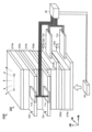
- 1 is a perspective view showing a configuration of an illumination device according to a first embodiment of the present invention.
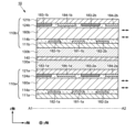
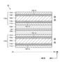
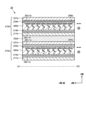
- 1 is a cross-sectional view showing a cross-sectional structure of a portion of a liquid crystal optical element according to a first embodiment of the present invention.
- 1 is a cross-sectional view showing a cross-sectional structure of a portion of a liquid crystal optical element according to a first embodiment of the present invention.
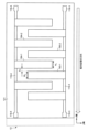
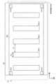
- 1 is a plan view showing an arrangement of electrodes of a liquid crystal optical element according to a first embodiment of the present invention.
- 1 is a plan view showing an arrangement of electrodes of a liquid crystal optical element according to a first embodiment of the present invention.
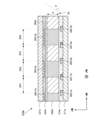
- FIG. 1 is a cross-sectional view showing a cross-sectional structure of a portion of a liquid crystal optical element according to a first embodiment of the present invention.
- 1 is a cross-sectional view for explaining light distribution using a liquid crystal optical element according to a first embodiment of the present invention.
- FIG. 1 is a cross-sectional view showing the orientation of liquid crystal in a liquid crystal layer in a liquid crystal optical element according to a first embodiment of the present invention.
- 3 is a diagram showing the relationship between each region and retardation in the liquid crystal optical element according to the first embodiment of the present invention.
- FIG. 1 is a cross-sectional view showing the orientation of liquid crystal in a liquid crystal layer in a liquid crystal optical element according to a first embodiment of the present invention.
- FIG. 13 is a perspective view showing a configuration of an illumination device according to a fourth embodiment of the present invention.
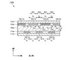
- FIG. 11 is a cross-sectional view showing a cross-sectional structure of a portion of a liquid crystal optical element according to a fourth embodiment of the present invention.
- Fig. 1 is a schematic perspective view showing the configuration of the illumination device 100.
- the first liquid crystal cell 110a and the second liquid crystal cell 110b have the same basic configuration and function. Therefore, when the first liquid crystal cell 110a and the second liquid crystal cell 110b are not distinguished, the liquid crystal cell is described as liquid crystal cell 110, and when the first liquid crystal cell 110a and the second liquid crystal cell 110b are distinguished, the liquid crystal cell is described as the first liquid crystal cell 110a and the second liquid crystal cell 110b.
- the adhesive layer 130a bonds and fixes the first liquid crystal cell 110a and the wave plate 140.
- the adhesive layer 130b bonds and fixes the wave plate 140 and the second liquid crystal cell 110b.
- the material for forming the adhesive layer 130a and the adhesive layer 130b can be an optically elastic resin.
- the optically elastic resin is, for example, an adhesive material containing an acrylic resin having translucency.
- the liquid crystal optical element 10 and the light source 30 are electrically connected to the control device 40.
- the control device 40 is electrically connected to the liquid crystal optical element 10 and the second liquid crystal cell 110b.
- the control device 40 is electrically connected via a first flexible wiring board 11a electrically connected to the terminal portion 12a of the first liquid crystal cell 110a and a second flexible wiring board 11b electrically connected to the terminal portion 12b of the second liquid crystal cell 110b.
- Light emitted from the light source 30 to the liquid crystal optical element 10 passes through the first liquid crystal cell 110a, the adhesive layer 130a, the wave plate 140, the adhesive layer 130b, and the second liquid crystal cell 110b, and is emitted from the second liquid crystal cell 110b. Details will be described later, but for example, the light passing through the liquid crystal optical element 10 is refracted in the x-axis direction or the y-axis direction based on the configuration of each electrode included in the liquid crystal cell 110 and the voltage supplied to each electrode from the control device 40.
- the lighting device 100 is capable of adjusting the light distribution direction and light distribution angle using the liquid crystal optical element 10, and can irradiate light having various adjusted light distribution directions and light distribution angles.
- FIG. 1 Configuration of the liquid crystal optical element 10
- Figures 2 and 3 are schematic cross-sectional views showing a cross-sectional structure of a portion of the liquid crystal optical element 10.
- Figure 2 is a schematic cross-sectional view in the zx plane cut along the line A1-A2 shown in Figure 1
- Figure 3 is a schematic cross-sectional view in the yz plane cut along the line B1-B2 shown in Figure 1.
- configurations that are the same as or similar to those in Figure 1 will be described as necessary.
- the first liquid crystal cell 110a includes a first substrate 111a, a second substrate 121a, a plurality of first transparent electrodes 181 (e.g., first transparent electrode 181-1a), a plurality of second transparent electrodes 182 (e.g., second transparent electrode 182-1a, second transparent electrode 182-2a), a plurality of third transparent electrodes 183 (e.g., third transparent electrode 183-1a, third transparent electrode 183-2a), a plurality of fourth transparent electrodes 184 (e.g., fourth transparent electrode 184-1a, fourth transparent electrode 184-2a), a first alignment film 114a, a second alignment film 124a, and a liquid crystal layer 160a.
- first transparent electrodes 181 e.g., first transparent electrode 181-1a
- second transparent electrode 182 e.g., second transparent electrode 182-1a, second transparent electrode 182-2a
- third transparent electrodes 183 e.g., third transparent electrode 183-1a, third transparent electrode 183-2a
- the multiple first transparent electrodes 181 and the multiple second transparent electrodes 182 are provided on the first substrate 111a and are covered with the first alignment film 114a. A portion of the first alignment film 114a is in contact with the first substrate 111a, the multiple first transparent electrodes 181, and the multiple second transparent electrodes 182.
- the plurality of third transparent electrodes 183 and the plurality of fourth transparent electrodes 184 are provided on the second substrate 121a and are covered with the second alignment film 124a. A portion of the second alignment film 124a is in contact with the second substrate 121a, the plurality of third transparent electrodes 183, and the plurality of fourth transparent electrodes 184.
- the first transparent electrode 181 and the second transparent electrode 182 on the first substrate 111a are arranged to face the third transparent electrode 183 and the fourth transparent electrode 184 on the second substrate 121a.
- a sealant (not shown) is provided around the periphery of the first substrate 111a and the second substrate 121a to bond the first substrate 111a and the second substrate 121a.
- a liquid crystal layer 160a containing liquid crystal is provided in a space surrounded by the first substrate 111a (more specifically, the first alignment film 114a), the second substrate 121a (more specifically, the second alignment film 124a), and the sealant.
- Each of the multiple first transparent electrodes 181, the multiple second transparent electrodes 182, the multiple third transparent electrodes 183, and the multiple fourth transparent electrodes 184 extends in the y-axis direction.
- the first transparent electrodes 181 and the multiple second transparent electrodes 182 are arranged alternately and repeatedly along the x-axis direction.
- the third transparent electrodes 183 and the fourth transparent electrodes 184 are arranged alternately and repeatedly along the x-axis direction.
- the first substrate 111a and the second substrate 121a may be rigid substrates having optical transparency, such as a glass substrate, a quartz substrate, or a sapphire substrate.
- the first substrate 111a and the second substrate 121a may be flexible substrates having optical transparency, such as a polyimide resin substrate, an acrylic resin substrate, a siloxane resin substrate, or a fluororesin substrate.
- the first transparent electrodes 181, the second transparent electrodes 182, the third transparent electrodes 183, and the fourth transparent electrodes 184 function as electrodes for forming an electric field in the liquid crystal layer 160a.
- the first transparent electrodes 181, the second transparent electrodes 182, the third transparent electrodes 183, and the fourth transparent electrodes 184 are made of a transparent conductive material such as indium tin oxide (ITO) or indium zinc oxide (IZO).
- the first transparent electrodes 181 provided in the first liquid crystal cell 110a and the second liquid crystal cell 110b overlap each other so that their extending directions (y-axis direction) match each other.
- the transparent electrodes of the same name provided in the first liquid crystal cell 110a and the second liquid crystal cell 110b overlap each other so that their extending directions (y-axis direction) match each other. That is, the lighting device 100 includes a configuration in which liquid crystal cells (the first liquid crystal cell 110a and the second liquid crystal cell 110b) of the same configuration are overlapped.
- the first liquid crystal cell 110a and the second liquid crystal cell 110b have the same basic configuration and function. Therefore, the first substrate 111a and the first substrate 111b, the second substrate 121a and the second substrate 121b, the plurality of first transparent electrodes 181 (e.g., the first transparent electrode 181-1a, the first transparent electrode 181-1b), the plurality of second transparent electrodes 182 (e.g., the second transparent electrode 182-1a, the second transparent electrode 182-2a, the second transparent electrode 182-1b, the second transparent electrode 182-2b), the plurality of third transparent electrodes 183 (e.g., the third transparent electrode 183-1a, the third transparent electrode 183-2a, the third transparent electrode 183-2b ...
- the plurality of first transparent electrodes 181 e.g., the first transparent electrode 181-1a, the first transparent electrode 181-1b
- the plurality of second transparent electrodes 182 e.g., the second transparent electrode 182-1a, the second transparent electrode 182-2a, the second transparent electrode 182-1b,
- the first and second alignment films 114a and 114b are used to describe the liquid crystal layers 160a and 160b.
- the components contained in the first liquid crystal cell 110a and the second liquid crystal cell 110b described above are not distinguished from one another, the components contained in the first liquid crystal cell 110a and the second liquid crystal cell 110b are described as a first substrate 111, a second substrate 121, a plurality of first transparent electrodes 181, a plurality of second transparent electrodes 182, a plurality of third transparent electrodes 183, a plurality of fourth transparent electrodes 184, a first alignment film 114, a second alignment film 124, and a liquid crystal layer 160.
- FIG. 4 is a schematic plan view showing the arrangement of a plurality of first transparent electrodes 181 and a plurality of second transparent electrodes 182 on the first substrate 111 of the liquid crystal optical element 10.
- FIG. 5 is a schematic plan view showing the arrangement of a plurality of third transparent electrodes 183 and a plurality of fourth transparent electrodes 184 on the second substrate 121 of the liquid crystal optical element 10.
- FIG. 6 is a cross-sectional view showing a cross-sectional structure of a part of the liquid crystal optical element 10. Note that FIG. 6 corresponds to the cross-sectional structure of the first liquid crystal cell 110a taken along the line A1-A2 shown in FIG. Configurations that are the same as or similar to those in FIG. 1 to FIG. 3 will be described as necessary.
- the cross-sectional structure of the first liquid crystal cell 110a is the same as the cross-sectional structure of the second liquid crystal cell 110b, and the cross-sectional structure of the first liquid crystal cell 110a will be described here, and the cross-sectional structure of the second liquid crystal cell 110b will be described as necessary.
- each electrode of the liquid crystal optical element 10 in a planar view will be described.
- a plurality of first transparent electrodes 181, a plurality of second transparent electrodes 182, a first terminal 119-1, and a second terminal 119-2 are provided on the first substrate 111.
- a fifth wiring 116-5, a sixth wiring 116-6, a plurality of first power supply terminals 118-1, a plurality of second power supply terminals 118-2, a third terminal 119-3, and a fourth terminal 119-4 are provided on the first substrate 111.
- the multiple first transparent electrodes 181 and multiple second transparent electrodes 182 are supplied with a control signal (electric potential) from the control device 40, and have the functions of transmitting, impeding transmission of, diffusing, and refracting the light emitted from the light source 30.
- the electrode width of the first transparent electrode 181 and the electrode width of the second transparent electrode 182 are a first width w1 .
- the inter-electrode distance (electrode spacing) in the x-axis direction between the first transparent electrode 181 and the second transparent electrode 182 is a first inter-electrode distance p1.
- the first width w1 is the same as the first inter-electrode distance p1 , but the first width w1 may be different from the first inter-electrode distance p1 .
- the electrode width of the first transparent electrode 181 and the electrode width of the second transparent electrode 182 may be different.
- the plurality of first transparent electrodes 181 are electrically connected to the first wiring 116-1, and the first wiring 116-1 is electrically connected to the first terminal 119-1.
- the first wiring 116-1 may be formed under the plurality of first transparent electrodes 181, or may be formed on the plurality of first transparent electrodes 181. Also, the first wiring 116-1 may be formed in the same layer as the plurality of first transparent electrodes 181.
- the plurality of second transparent electrodes 182 are electrically connected to the second wiring 116-2, and the second wiring 116-2 is electrically connected to the second terminal 119-2.
- the second wiring 116-2 may be formed under the plurality of second transparent electrodes 182, or may be formed on the plurality of second transparent electrodes 182.
- the second wiring 116-2 may be formed in the same layer as the plurality of second transparent electrodes 182.
- the multiple first transparent electrodes 181 and multiple second transparent electrodes 182 of the lighting device 100 are formed in the same layer as the first wiring 116-1 and the second wiring 116-2.
- the first alignment film 114 disposed on the first substrate 111 is aligned in the x-axis direction (the direction indicated by the hollow arrow in FIG. 4).
- the long axes of the liquid crystal molecules on the first substrate 111 side among those constituting the liquid crystal layer 160 are aligned along the x-axis direction.
- the alignment direction of the first alignment film 114 (x-axis direction) is perpendicular to the extension direction (y-axis direction) of the multiple first transparent electrodes 181 and the multiple second transparent electrodes 182.
- a plurality of third transparent electrodes 183, a plurality of fourth transparent electrodes 184, a third wiring 116-3, a fourth wiring 116-4, a plurality of third power supply terminals 118-3, and a plurality of fourth power supply terminals 118-4 are provided on the second substrate 121.
- the plurality of third transparent electrodes 183 and the plurality of fourth transparent electrodes 184 are supplied with a control signal (electric potential) from the control device 40, and have the functions of transmitting, impeding transmission of, diffusing, and refracting the light emitted from the light source 30.
- the plurality of third transparent electrodes 183 include a third transparent electrode 183-1 and a third transparent electrode 183-2.
- the plurality of fourth transparent electrodes 184 include a fourth transparent electrode 184-1 and a fourth transparent electrode 184-2.
- the major axes of the plurality of third transparent electrodes 183 and the plurality of fourth transparent electrodes 184 extend in the y-axis direction, and the third transparent electrodes 183 and the fourth transparent electrodes 184 are alternately arranged along the x-axis direction.
- the electrode width of the third transparent electrode 183 and the electrode width of the fourth transparent electrode 184 are the second width w2 .
- the inter-electrode distance (electrode spacing) between the third transparent electrode 183 and the fourth transparent electrode 184 in the x-axis direction is the second inter-electrode distance p2 .
- the second width w2 is wider (thicker) than the first width w1
- the second inter-electrode distance p2 is narrower (thinner) than the first inter-electrode distance p1 .
- the electrode width of the third transparent electrode 183 and the electrode width of the fourth transparent electrode 184 may be different from each other.
- the plurality of third transparent electrodes 183 are electrically connected to the third wiring 116-3, and the third wiring 116-3 is electrically connected to the plurality of third power supply terminals 118-3.
- the plurality of fourth transparent electrodes 184 are electrically connected to the fourth wiring 116-4, and the fourth wiring 116-4 is electrically connected to the plurality of fourth power supply terminals 118-4.
- the third wiring 116-3 may be formed under the plurality of third transparent electrodes 183, or may be formed on the plurality of third transparent electrodes 183. Furthermore, the third wiring 116-3 may be formed in the same layer as the plurality of third transparent electrodes 183.
- the fourth wiring 116-4 may be formed under the plurality of fourth transparent electrodes 184, or may be formed on the plurality of fourth transparent electrodes 184.
- the first transparent electrodes 181 and the second transparent electrodes 182 face the third transparent electrodes 183 and the fourth transparent electrodes 184 via the liquid crystal layer 160a.
- the direction in which the first transparent electrodes 181 and the second transparent electrodes 182 extend is parallel to the direction in which the third transparent electrodes 183 and the fourth transparent electrodes 184 extend (y-axis direction).
- each of the first power supply terminals 118-1 is electrically connected to the corresponding third power supply terminal 118-3, and each of the second power supply terminals 118-2 is electrically connected to the corresponding fourth power supply terminal 118-4.
- the first wiring 116-1 is electrically connected to the third wiring 116-3
- the second wiring 116-2 is electrically connected to the fourth wiring 116-4.
- the first power supply terminal 118-1 and the third power supply terminal 118-3, and the second power supply terminal 118-2 and the fourth power supply terminal 118-4 can be electrically connected using silver paste or conductive particles.
- the conductive particles include metal-coated particles.
- the terminal portion 12a can be easily attached to the first flexible wiring board 11a and can be easily electrically connected.
- the multiple first transparent electrodes 181 are supplied with a control signal (electric potential) from the control device 40 (see FIG. 1) via the first flexible wiring board 11a, the terminal portion 12a, the first terminal 119-1, and the first wiring 116-1.
- the multiple second transparent electrodes 182 are supplied with a control signal (electric potential) from the control device 40 via the first flexible wiring board 11a, the terminal portion 12a, the second terminal 119-2, and the second wiring 116-2.
- the third transparent electrodes 183 are supplied with a control signal (electric potential) from the control device 40 via the first flexible wiring board 11a, the terminal portion 12a, the third terminal 119-3, the fifth wiring 116-5, the first power supply terminals 118-1, the third wiring 116-3, and the third power supply terminals 118-3.
- the fourth transparent electrodes 184 are supplied with a control signal (electric potential) from the control device 40 via the first flexible wiring board 11a, the terminal portion 12a, the fourth terminal 119-4, the sixth wiring 116-6, the second power supply terminals 118-2, the fourth wiring 116-4, and the fourth power supply terminals 118-4.
- each electrode in the second liquid crystal cell 110b is also supplied with a control signal (electric potential) from the control device 40.
- a photospacer may be formed on the side of the first substrate 111 facing the second substrate 121, or on the side of the second substrate 121 facing the first substrate 111. By including a photospacer, the lighting device 100 can maintain a constant distance between the first substrate 111 and the second substrate 121.
- a metal material can be used as a material for forming the first wiring 116-1, the second wiring 116-2, the third wiring 116-3, the fourth wiring 116-4, the fifth wiring 116-5, the sixth wiring 116-6, the multiple first power supply terminals 118-1, the multiple third power supply terminals 118-3, the multiple second power supply terminals 118-2, the multiple fourth power supply terminals 118-4, the first terminal 119-1, the second terminal 119-2, the third terminal 119-3, and the fourth terminal 119-4.
- the metal material is, for example, aluminum or molybdenum.
- the material forming the first transparent electrodes 181 and the second transparent electrodes 182 is ITO or IZO
- the first transparent electrodes 181 are arranged so as to overlap on the first wiring 116-1 (opposite side to the first substrate 111)
- the second transparent electrodes 182 are arranged so as to overlap on the second wiring 116-2 (opposite side to the first substrate 111).
- the material forming the first transparent electrodes 181 and the second transparent electrodes 182 is ITO or IZO
- the first transparent electrodes 181 and the second transparent electrodes 182 have high resistance to corrosion.
- first transparent electrodes 181 and multiple second transparent electrodes 182 which are highly resistant to corrosion, on the first wiring 116-1, second wiring 116-2, first terminal 119-1, and second terminal 119-2 (on the side opposite the first substrate 111) which are made of a metal material, corrosion of the first wiring 116-1, second wiring 116-2, first terminal 119-1, and second terminal 119-2 can be suppressed.
- the first transparent electrode 181-1a is sandwiched between two adjacent second transparent electrodes 182-1a and 182-2a.
- the first transparent electrode 181-1a overlaps along the z-axis direction with the end of the fourth transparent electrode 184-1a facing the third transparent electrode 183-2a, the space between the fourth transparent electrode 184-1a and the third transparent electrode 183-2a, and the end of the third transparent electrode 183-2a facing the fourth transparent electrode 184-1a.
- the space between the first transparent electrode 181-1a and the second transparent electrode 182-1a overlaps with the fourth transparent electrode 184-1a along the z-axis direction.
- the space between the first transparent electrode 181-1a and the second transparent electrode 182-2a overlaps with the third transparent electrode 183-2a along the z-axis direction.
- the second transparent electrode 182-1a overlaps along the z-axis direction with the end of the third transparent electrode 183-1a facing the fourth transparent electrode 184-1a, the space between the third transparent electrode 183-1a and the fourth transparent electrode 184-1a, and the end of the fourth transparent electrode 184-1a facing the third transparent electrode 183-1a.
- the second transparent electrode 182-2a is configured in the same manner as the second transparent electrode 182-1a.
- the third transparent electrode 183-2a is sandwiched between two adjacent fourth transparent electrodes 184-1a and 184-2a.
- the fourth transparent electrode 184-1a is sandwiched between two adjacent third transparent electrodes 183-1a and 183-2a.
- the first liquid crystal cell 110a includes a plurality of first regions ZN1 and a plurality of second regions ZN2.
- the plurality of first regions ZN1 and the plurality of second regions ZN2 are arranged alternately along the x-axis direction.
- the first region ZN1 is adjacent to the second region ZN2.
- the first region ZN1 also includes a region where the space between the first transparent electrode 181-1a and the second transparent electrode 182-1a overlaps with the fourth transparent electrode 184-1a along the z-axis direction.
- the first region ZN1 also includes a region where the space between the first transparent electrode 181-1a and the second transparent electrode 182-2a overlaps with the third transparent electrode 183-2a along the z-axis direction.
- the width OV2 is the width where the first transparent electrode 181-1a overlaps with the end of the fourth transparent electrode 184-1a on the third transparent electrode 183-2a side along the z-axis direction.
- the width OV3 is the width along the z-axis direction where the first transparent electrode 181-1a overlaps with the end of the third transparent electrode 183-2a on the fourth transparent electrode 184-1a side.
- the second region ZN2 includes, along the z-axis direction, a region where the first transparent electrode 181-1a overlaps with the end of the fourth transparent electrode 184-1a on the side of the third transparent electrode 183-2a, a region where the first transparent electrode 181-1a overlaps with the space between the fourth transparent electrode 184-1a and the third transparent electrode 183-2a, and a region where the first transparent electrode 181-1a overlaps with the end of the third transparent electrode 183-2a on the side of the fourth transparent electrode 184-1a.
- the components contained in the first liquid crystal cell 210a and the second liquid crystal cell 210b described above are not distinguished from one another, the components contained in the first liquid crystal cell 210a and the second liquid crystal cell 210b are described as a first substrate 211, a second substrate 221, a plurality of first transparent electrodes 281, a plurality of second transparent electrodes 282, a plurality of third electrodes 283, a plurality of fourth transparent electrodes 284, a first alignment film 214, a second alignment film 224, and a liquid crystal layer 260.
- the cross-sectional structure of the first liquid crystal cell 210a is the same as the cross-sectional structure of the second liquid crystal cell 210b, and the cross-sectional structure of the first liquid crystal cell 210a will be described here, and the cross-sectional structure of the second liquid crystal cell 210b will be described as necessary.
- each electrode of the liquid crystal optical element 20 in a planar view will be described.
- a plurality of first transparent electrodes 281, a plurality of second transparent electrodes 282, a first terminal 219-1, and a second terminal 219-2 are provided on the first substrate 211.
- a fifth wiring 216-5, a sixth wiring 216-6, a plurality of first power supply terminals 218-1, a plurality of second power supply terminals 218-2, and a third terminal 219-3 are provided on the first substrate 211.
- the multiple first transparent electrodes 281 and multiple second transparent electrodes 282 are supplied with a control signal (electric potential) from the control device 40, and have the functions of transmitting, impeding transmission of, diffusing, and refracting the light emitted from the light source 30.
- the fifth wiring 216-5 is electrically connected to the plurality of first power supply terminals 218-1, the sixth wiring 216-6, the plurality of second power supply terminals 218-2, and the third terminal 219-3.
- the first alignment film 214 disposed on the first substrate 211 is aligned in the x-axis direction (the direction indicated by the hollow arrow in FIG. 19).
- the long axes of the liquid crystal molecules on the first substrate 211 side among those constituting the liquid crystal layer 260 are aligned along the x-axis direction.
- the alignment direction of the first alignment film 214 (x-axis direction) is perpendicular to the extension direction (y-axis direction) of the multiple first transparent electrodes 281 and the multiple second transparent electrodes 282.
- the fourth width w4 is wider (thicker) than the third width w3
- the third inter-electrode distance p3 is narrower (thinner) than the fourth inter-electrode distance p4
- the cell gap d is narrower than the fourth width w4 .
- each of the multiple first power supply terminals 218-1 is electrically connected to the corresponding third power supply terminal 218-3
- each of the multiple second power supply terminals 218-2 is electrically connected to the corresponding fourth power supply terminal 218-4.
- the first wiring 216-1 and the sixth wiring 216-6 are electrically connected to the multiple third electrodes 283 and the fourth transparent electrode 284.
- the first power supply terminal 218-1 and the third power supply terminal 218-3, and the second power supply terminal 218-2 and the fourth power supply terminal 218-4 can be electrically connected using silver paste or conductive particles.
- the conductive particles include particles coated with a metal.
- the length of the second substrate 221 along the x-axis direction is shorter than the length of the first substrate 211 along the x-axis direction.
- the first terminal 219-1, the second terminal 219-2, and the third terminal 219-3 are provided on the terminal portion 22 on the first substrate 211.
- the first terminal 219-1, the second terminal 219-2, and the third terminal 219-3 are exposed and not covered by the second substrate 221.
- the terminal portion 22a can be easily attached to the first flexible wiring board 11a and can be easily electrically connected.
- the multiple first transparent electrodes 281 are supplied with a control signal (electric potential) from the control device 40 (see FIG. 16) via the first flexible wiring board 11a, the terminal portion 22a, the first terminal 219-1, and the first wiring 216-1.
- the multiple second transparent electrodes 282 are supplied with a control signal (electric potential) from the control device 40 via the first flexible wiring board 11a, the terminal portion 22a, the second terminal 219-2, and the second wiring 216-2.
- the third electrodes 283 and the fourth transparent electrodes 284 are supplied with a control signal (electric potential) from the control device 40 via the first flexible wiring board 11a, the terminal portion 22a, the third terminal 219-3, the fifth wiring 216-5, the first power supply terminals 218-1, the sixth wiring 216-6, the second power supply terminals 218-2, the third power supply terminals 218-3, and the fourth power supply terminals 218-4.
- the terminal portion 22b of the second liquid crystal cell 210b can also be easily attached to the second flexible wiring board 11b and easily electrically connected.
- each electrode in the second liquid crystal cell 210b is also supplied with a control signal (electric potential) from the control device 40.
- a metal material can be used as a material for forming the first wiring 216-1, the second wiring 216-2, the fifth wiring 216-5, the sixth wiring 216-6, the multiple first power supply terminals 218-1, the multiple third power supply terminals 218-3, the multiple second power supply terminals 218-2, the multiple fourth power supply terminals 218-4, the first terminal 219-1, the second terminal 219-2, the third terminal 219-3, and the multiple third electrodes 283.
- the metal material is, for example, aluminum or molybdenum.
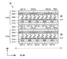
- the first transparent electrode 281-1a is sandwiched between two adjacent second transparent electrodes 282-1a and 282-2a.
- the first transparent electrode 281-1a overlaps along the z-axis direction with the end of the third electrode 283-2a on the third electrode 283-1a side, and with the space between the third electrodes 283-1a and 283-2a.
- the second transparent electrode 282-1a overlaps along the z-axis direction with the end of the third electrode 283-1a facing the third electrode 283-2a, and with the space between the third electrodes 283-1a and 283-2a.
- the first transparent electrode 281-2a is configured similarly to the first transparent electrode 281-1a.
- the second transparent electrode 282-2a and the second transparent electrode 282-3a are configured similarly to the second transparent electrode 282-1a.
- the third electrode 283-2a is sandwiched between two adjacent third electrodes 283-1a and a third transparent electrode 183-3a.
- a fourth transparent electrode 284 is disposed between the third electrodes 283-1a and 283-2a, between the third electrodes 283-2a and 283-3a, on the top surface of the third electrode 283-1a, on the top surface of the third electrode 283-2a, and on the top surface of the third electrode 283-3a.
- the first liquid crystal cell 210a includes a plurality of first regions ZN1 and a plurality of second regions ZN2.
- the plurality of first regions ZN1 and the plurality of second regions ZN2 are arranged alternately along the x-axis direction.
- the first region ZN1 is adjacent to the second region ZN2.
- the first region ZN1 also includes, along the z-axis direction, a region where the space between the first transparent electrode 281-1a and the second transparent electrode 282-1a overlaps with the space between the third electrode 283-1a and the third electrode 283-2a, a region where the space between the third electrode 283-1a and the third electrode 283-2a overlaps with the end of the first transparent electrode 281-1a on the side of the second transparent electrode 282-1a, and a region where the space between the third electrode 283-1a and the third electrode 283-2a overlaps with the end of the second transparent electrode 282-1a on the side of the first transparent electrode 281-1a.
- the first region ZN1 includes, along the z-axis direction, a region where the space between the first transparent electrode 281 and the second transparent electrode 282 overlaps with the space between adjacent third electrodes 283, a region where the space between adjacent third electrodes 283 overlaps with the end of the first transparent electrode 281, and a region where the space between adjacent third electrodes 283 overlaps with the end of the second transparent electrode 282.
- the second region ZN2 includes, along the z-axis direction, a region where the space between the first transparent electrode 281-1a and the second transparent electrode 282-2a overlaps with the opposing third electrode 283-2a, a region where the end of the first transparent electrode 281-1a on the second transparent electrode 282-2a side overlaps with the end of the opposing third electrode 283-2a on the third electrode 283-1a side, and a region where the end of the second transparent electrode 282-2a on the first transparent electrode 281-1a side overlaps with the end of the opposing third electrode 283-2a on the third electrode 283-1a side.
- the second region ZN2 includes, along the z-axis direction, a region where the space between the first transparent electrode 281 and the second transparent electrode 282 overlaps with the opposing third electrode 283, a region where the end of the first transparent electrode 281 overlaps with the opposing third electrode 283, and a region where the end of the second transparent electrode 282 overlaps with the opposing third electrode 283.
- the width OV 5 is the width at which the end of the first transparent electrode 281-1a on the second transparent electrode 282-2a side overlaps with the end of the third electrode 283-2a on the third electrode 283-1a side along the z-axis direction. Also, the width OV 5 is the width at which the end of the first transparent electrode 281-2a on the second transparent electrode 282-3a side overlaps with the end of the third electrode 283-3a on the third electrode 283-2a side along the z-axis direction. In other words, the width OV 5 is the width at which the first transparent electrode 281 overlaps with the end of the third electrode 283 along the z-axis direction.
- Width OV6 is the width at which the end of second transparent electrode 282-2a on the first transparent electrode 281-1a side overlaps with the end of third electrode 283-2a on the third electrode 283-3a side along the z-axis direction. Width OV6 is also the width at which the end of second transparent electrode 282-3a overlaps with the end of third electrode 283-3a along the z-axis direction. In other words, width OV6 is the width at which the end of second transparent electrode 282 overlaps with the end of third electrode 283.
- the cell gap d may be the distance between the surface where the liquid crystal layer 260a and the first alignment film 214a contact and the surface where the liquid crystal layer 260a and the first alignment film 214a contact, or may be the distance between the first substrate 211a and the second substrate 221a.
- the cell gap d of the lighting device 200 is the distance between the surface where the liquid crystal layer 260a and the first alignment film 214a contact and the surface where the liquid crystal layer 260a and the first alignment film 214a contact.
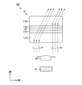
- Fig. 22 is a cross-sectional view for explaining the light distribution using the liquid crystal optical element 20.
- Fig. 23 is a diagram showing the relationship between each region in the first liquid crystal cell 210a and the phase difference.
- Figs. 24 and 25 are timing charts showing the voltages supplied to each terminal included in the liquid crystal optical element 20. Configurations that are the same as or similar to those in Figs. 1 to 21 will be described as necessary.
- the liquid crystal optical element 20 will be described in a state in which a potential is supplied to each transparent electrode of the first liquid crystal cell 210a.
- the configuration and function of the second liquid crystal cell 210b are similar to those of the first liquid crystal cell 210a, and will therefore be described as necessary.
- first electric field occurs between the adjacent first transparent electrodes 281 and second transparent electrodes 282.
- the multiple third electrodes 283 and fourth transparent electrodes 284 are supplied with the same control signal (electric potential) as either the multiple first transparent electrodes 281 or the multiple second transparent electrodes 282 from the control device 40.
- the first electric field is called a transverse electric field.
- the first polarized light 61 incident on the incident surface 63 of the first liquid crystal cell 210e is bent and transmitted, rotated by 90 degrees by the wave plate 240, transmitted through the second liquid crystal cell 210f, and emitted from the liquid crystal optical element 20A. Since the second polarized light 62 is rotated 90 degrees from the first polarized light 61, it passes through the first liquid crystal cell 210e, rotates 90 degrees at the wave plate 240, is bent and passes through the second liquid crystal cell 210f in the same manner as the first polarized light 61, and is emitted from the liquid crystal optical element 20A.
- the first liquid crystal cell 210a, the adhesive layer 230a, the second liquid crystal cell 210b, the adhesive layer 230b, the third liquid crystal cell 210c, the adhesive layer 230c, and the fourth liquid crystal cell 210d are stacked in this order along the z-axis direction, starting from the side closest to the light source.
- the first liquid crystal cell 210a, the second liquid crystal cell 210b, the third liquid crystal cell 210c, and the fourth liquid crystal cell 210d have the same basic configuration and function.
- the configuration and function of the first liquid crystal cell 210a and the second liquid crystal cell 210b are similar to the configuration and function of the first liquid crystal cell 210a and the second liquid crystal cell 210b of the lighting device 200, and will be described as necessary.
- Adhesive layers 230a to 230c can be made of the same material as adhesive layer 130a.
- the light source 30 and the control device 40 have the same configuration as the lighting device 100.
- the control device 40 controls the liquid crystal optical element 20B and the light source 30.
- the control device 40 can supply control signals (electric potentials) capable of controlling the light distribution direction and orientation angle of light to the first liquid crystal cell 210a to the fourth liquid crystal cell 210d of the liquid crystal optical element 20B, and can supply control signals (electric potentials) capable of controlling the lighting and brightness of the light source 30.
- the liquid crystal optical element 20B and the light source 30 are electrically connected to the control device 40.
- the control device 40 is electrically connected via a third flexible wiring board 11c electrically connected to the terminal portion 22c of the first liquid crystal cell 210a, a second flexible wiring board 11b electrically connected to the terminal portion 22b of the second liquid crystal cell 210b, a third flexible wiring board 11c electrically connected to the terminal portion 22c of the third liquid crystal cell 210c, and a fourth flexible wiring board 11d electrically connected to the terminal portion 22d of the fourth liquid crystal cell 210d.
- Figure 29 is a schematic cross-sectional view in the zx plane taken along the line E1-E2 shown in Figure 28.
- the third liquid crystal cell 210c has the same structure and function as the first liquid crystal cell 210a
- the fourth liquid crystal cell 210d has the same structure and function as the second liquid crystal cell 210b.
- the lighting device 200B has a structure in which the liquid crystal optical element 10 (the first liquid crystal cell 210a and the second liquid crystal cell 210b having the same structure) described in the lighting device 200 is rotated 90 degrees and stacked with liquid crystal optical elements (the third liquid crystal cell 210c and the fourth liquid crystal cell 210d having the same structure) having the same structure as the liquid crystal optical element 10.
- the third liquid crystal cell 210c includes a first substrate 211c, a second substrate 221c, a plurality of first transparent electrodes (not shown), a plurality of second transparent electrodes 282 (e.g., second transparent electrode 282-1c), a plurality of third electrodes 283 (e.g., third electrode 283-1c), a fourth transparent electrode 284c, a first alignment film 214c, a second alignment film 224c, and a liquid crystal layer 260c.
- the fourth liquid crystal cell 210d includes a first substrate 211d, a second substrate 221d, a plurality of first transparent electrodes (not shown), a plurality of second transparent electrodes 282 (e.g., second transparent electrode 282-1d), a plurality of third electrodes 283 (e.g., third electrode 283-1d), a fourth transparent electrode 284d, a first alignment film 214d, a second alignment film 224d, and a liquid crystal layer 260d.
- Each component of the fourth liquid crystal cell 210d is similar to each component of the third liquid crystal cell 210c.
- the configurations of the first substrate 211c, the second substrate 221c, the plurality of first transparent electrodes 281, the plurality of second transparent electrodes 282, the first alignment film 214c, the second alignment film 224c, and the liquid crystal layer 260c are similar to the configurations of the first substrate 111a, the second substrate 121a, the plurality of first transparent electrodes 181, the plurality of second transparent electrodes 182, the first alignment film 114a, the second alignment film 124a, and the liquid crystal layer 160a. Therefore, a detailed description of the third liquid crystal cell 210c and the fourth liquid crystal cell 210d will be omitted.
- the direction in which the multiple first transparent electrodes, multiple second transparent electrodes 282, and multiple third electrodes 283 included in the third liquid crystal cell 210c and the fourth liquid crystal cell 210d extend is perpendicular to the direction in which the multiple first transparent electrodes, multiple second transparent electrodes 282, and multiple third electrodes 283 included in the first liquid crystal cell 210a and the second liquid crystal cell 210b extend.
- the direction (x-axis direction) of the alignment treatment of the first substrate 211 of the first liquid crystal cell 210a and the second liquid crystal cell 210b is perpendicular to the direction (y-axis direction) of the alignment treatment of the first substrate 211 of the third liquid crystal cell 210c and the fourth liquid crystal cell 210d.
- the direction (y-axis direction) of the alignment treatment of the second substrate 221 of the first liquid crystal cell 210a and the second liquid crystal cell 210b is perpendicular to the direction (x-axis direction) of the alignment treatment of the second substrate 221 of the third liquid crystal cell 210c and the fourth liquid crystal cell 210d.
- the first liquid crystal cell 210a bends the first polarized light 61 parallel to the y-axis direction in the x-axis direction and rotates it
- the second liquid crystal cell 210b bends the second polarized light 62 parallel to the x-axis direction in the x-axis direction and rotates it
- the third liquid crystal cell 210c bends the first polarized light 61 parallel to the y-axis direction in the y-axis direction and advances it
- the fourth liquid crystal cell 210d bends the second polarized light 62 parallel to the x-axis direction in the y-axis direction and rotates it.
- the lighting device 200B can bend light in two directions, the x-axis direction and the y-axis direction.
- the lighting device 200B can supply a potential to each electrode included in the liquid crystal optical element 20B, thereby causing light bent at a control angle ⁇ corresponding to the supplied potential to be emitted from the liquid crystal optical element 20B. Therefore, the lighting device 200B can adjust the light distribution direction and light distribution angle using the liquid crystal optical element 20B, and can irradiate light having various adjusted light distribution directions and light distribution angles.
- liquid crystal optical element and lighting device exemplified as one embodiment of the present invention may be combined as appropriate as long as they are not mutually inconsistent. Furthermore, the various configurations of the liquid crystal optical element and lighting device exemplified as one embodiment of the present invention may be interchanged as appropriate as long as they are not mutually inconsistent. Liquid crystal optical elements and lighting devices disclosed in this specification and drawings, to which a person skilled in the art has appropriately added or deleted components or modified the design, or to which a process has been added, omitted, or conditions have been changed, are also included within the scope of the present invention as long as they comprise the gist of the present invention.
Landscapes
- Physics & Mathematics (AREA)
- Nonlinear Science (AREA)
- Chemical & Material Sciences (AREA)
- Crystallography & Structural Chemistry (AREA)
- General Physics & Mathematics (AREA)
- Optics & Photonics (AREA)
- Mathematical Physics (AREA)
- Liquid Crystal (AREA)
Abstract
本発明の液晶光学素子(10)は、第1の液晶セル(110a)、及び、第1の液晶セル(110a)に重なる第2の液晶セル(110b)を有し、第1の液晶セル(110a)及び第2の液晶セル(110b)のそれぞれは、第1の基板(111a,111b)、第1の基板(111a,111b)上に配置された第1の電極(181)及び第2の電極(182)、第1の基板(111a,111b)に対向して配置される第2の基板(121a,121b)、第2の基板(121a,121b)上に配置された第3の電極(183)及び第4の電極(184)、及び、第1の基板(111a,111b)と第2の基板(121a,121b)との間に配置される液晶層(160a,160b)を有し、第1の電極(181)及び第2の電極(182)は第1の方向(x軸)に平行に交互に配置され、第3の電極(183)及び第4の電極(184)は第1の方向(x軸)に平行に交互に配置され、第1の電極(181)は、第3の電極(183)の第1の端部、第3の電極(183)と第4の電極(184)との間のスペース、及び、第4の電極(184)の第1の端部と重畳し、第4の電極(184)は、第1の電極(181)と第2の電極(182)との間のスペース、第2の電極(182)の第1の端部と重畳する。
Description
本発明の一実施形態は、液晶の光学特性を利用し配光を制御する素子、及び液晶の光学特性を利用し配光を制御する素子を含む照明装置に関する。
液晶に電圧を供給し液晶の屈折率を変化させ、焦点距離を電気的に制御する液晶を用いた光学素子(液晶光学素子)として、液晶レンズが知られている。例えば、特許文献1には、液晶レンズを用いて、光の広がりを制御可能な照明装置が記載されている。
例えば、近年、光の配光する方向(配向方向)及び光の配光する角度(配向角)の制御が可能な照明装置が求められている。
本発明の一実施形態は、上記問題に鑑み、光の配光方向及び光の配光角を制御可能な液晶光学素子及び照明装置を提供することを目的の一つとする。
本発明の一実施形態に係る液晶光学素子は、第1の液晶セル、及び、前記第1の液晶セルに重なる第2の液晶セル、を有し、前記第1の液晶セル、及び前記第2の液晶セルのそれぞれは、第1の基板、前記第1の基板上に配置された第1の電極及び第2の電極、前記第1の基板に対向して配置される第2の基板、前記第2の基板上に配置された第3の電極及び第4の電極、及び、前記第1の基板と前記第2の基板との間に配置される液晶層を有し、前記第1の電極及び前記第2の電極は、第1の方向に平行に交互に配置され、前記第1の方向に交差する第2の方向に延在し、前記第3の電極及び第4の電極は、前記第1の方向に平行に交互に配置され、前記第2の方向に延在し、前記第1の電極は、前記第1の方向及び前記第2の方向と交差する第3の方向において、前記第3の電極の第1の端部、前記第3の電極と前記第4の電極との間のスペース、及び、前記第4の電極の第1の端部と重畳し、前記第4の電極は、前記第3の方向において、前記第1の電極と前記第2の電極との間のスペース、前記第2の電極の第1の端部と重畳する。
本発明の一実施形態に係る照明装置は、第1の液晶セル、及び、前記第1の液晶セルに重なる第2の液晶セル、を有し、前記第1の液晶セル、及び前記第2の液晶セルのそれぞれは、第1の基板、前記第1の基板上に配置された第1の電極及び第2の電極、前記第1の基板に対向して配置される第2の基板、前記第2の基板上に配置された第3の電極及び第4の電極、及び、前記第1の基板と前記第2の基板との間に配置される液晶層を有し、前記第1の電極及び前記第2の電極は、第1の方向に平行に交互に配置され、前記第1の方向に交差する第2の方向に延在し、前記第3の電極及び第4の電極は、前記第1の方向に平行に交互に配置され、前記第2の方向に延在し、前記第1の電極は、前記第1の方向及び前記第2の方向と交差する第3の方向において、前記第3の電極の第1の端部、前記第3の電極と前記第4の電極との間のスペース、及び、前記第4の電極の第1の端部と重畳し、前記第4の電極は、前記第3の方向において、前記第1の電極と前記第2の電極との間のスペース、前記第2の電極の第1の端部と重畳する液晶光学素子と、前記液晶光学素子と電気的に接続され、前記第1の電極、前記第2の電極、前記第3の電極及び前記第4の電極に制御信号を供給する制御装置含む。
本発明の一実施形態に係る液晶光学素子は、第1の液晶セル、及び、前記第1の液晶セルに重なる第2の液晶セル、を有し、前記第1の液晶セル、及び前記第2の液晶セルのそれぞれは、第1の基板、前記第1の基板上に配置された第1の電極及び第2の電極、前記第1の基板に対向して配置される第2の基板、前記第2の基板上に配置された第3の電極及び第4の電極、及び、前記第1の基板と前記第2の基板との間に配置される液晶層を有し、前記第1の電極及び前記第2の電極は、第1の方向に平行に交互に配置され、前記第1の方向に交差する第2の方向に延在し、前記第3の電極は、前記第1の方向に平行に配置され、前記第2の方向に延在し、前記第4の電極は、前記第3の電極を覆うように前記第2の基板上に配置され、前記第1の電極は、前記第1の方向及び前記第2の方向と交差する第3の方向において、前記第3の電極の第1の端部、及び、前記第3の電極間のスペースと重畳し、前記第3の電極は、前記第3の方向において、前記第1の電極と前記第2の電極との間のスペース、前記第2の電極の第1の端部と重畳し、前記第3の電極間のスペースは、前記第1の電極と前記第2の電極とは異なる第2の電極との間のスペースと重畳する。
以下、本発明の実施の形態を、図面等を参照しながら説明する。但し、本発明は多くの異なる態様で実施することが可能であり、以下に例示する実施の形態の記載内容に限定して解釈されるものではない。図面は説明をより明確にするため、実際の態様に比べ、各部の幅、厚さ、形状等について模式的に表される場合があるが、あくまで一例であって、本開示の解釈を限定するものではない。また、本明細書と各図において、既出の図に関して前述したものと同様の要素には、同一の符号、数字の後にa、b、A、Bなどのアルファベット、又は、数字の後にハイフンと数字を付して、詳細な説明を適宜省略することがある。さらに各要素に対する「第1」、「第2」と付記された文字は、各要素を区別するために用いられる便宜的な標識であり、特段の説明がない限りそれ以上の意味を有しない。
本明細書において、ある部材又は領域が他の部材又は領域の「上に(又は下に)」あるとする場合、特段の限定がない限りこれは他の部材又は領域の直上(又は直下)にある場合のみでなく他の部材又は領域の上方(又は下方)にある場合を含み、すなわち、他の部材又は領域の上方(又は下方)において間に別の構成要素が含まれている場合も含む。
また、本明細書において、ある一つの膜を加工して複数の構造体を形成した場合、各々の構造体は異なる機能、役割を有する場合があり、また、各々の構造体はそれが形成される下地が異なる場合がある。しかしながら、これら複数の構造体は、同一の工程で同一層として形成された膜に由来するものであり、同一の材料を有する。従って、これら複数の膜は同一層に存在しているものと定義する。
また、本明細書において「αはA、B又はCを含む」、「αはA,B及びCのいずれかを含む」、「αはA,B及びCからなる群から選択される一つを含む」、といった表現は、特に明示が無い限り、αはA乃至Cの複数の組み合わせを含む場合を排除しない。さらに、これらの表現は、αが他の要素を含む場合も排除しない。
本明細書において、x軸方向、x軸方向と交差するy軸方向、x軸及びy軸と交差するz軸を、それぞれ、第1の方向、第2の方向、第3の方向と呼ぶ場合がある。また、x軸はy軸と直交し、z軸はxy平面(x軸及びy軸)に垂直である。
本明細書において、直交、垂直、平行、同一及び一致という表記を用いている場合、直交、垂直、同一及び一致には、設計の範囲での誤差が含まれてもよい。
<第1実施形態>
<1-1.照明装置100の構成>
図1を参照し、第1実施形態に係る照明装置100の構成の概略を説明する。図1は照明装置100の構成を示す模式的な斜視図である。
<1-1.照明装置100の構成>
図1を参照し、第1実施形態に係る照明装置100の構成の概略を説明する。図1は照明装置100の構成を示す模式的な斜視図である。
図1に示されるように、照明装置100は、液晶光学素子10、光源30、及び制御装置40を含む。詳細は後述するが、液晶光学素子10は、第1の液晶セル110a、接着層130a、波長板140、接着層130b、及び第2の液晶セル110bを含む。接着層130aは第1の液晶セル110aと波長板140との間に設けられ、接着層130bは波長板140と第2の液晶セル110bとの間に設けられる。第1の液晶セル110a、接着層130a、波長板140、接着層130b、及び第2の液晶セル110bは、z軸方向に沿って、光源に近い方からこの順に位置するように積層されている。
第1の液晶セル110a及び第2の液晶セル110bの基本的な構成及び機能は同じである。よって、第1の液晶セル110a及び第2の液晶セル110bが区別されない場合には、液晶セルは液晶セル110として説明され、第1の液晶セル110a及び第2の液晶セル110bが区別される場合には、液晶セルは第1の液晶セル110a及び第2の液晶セル110bとして説明される。
接着層130aは、第1の液晶セル110a及び波長板140を接着し、固定する。接着層130bは、波長板140及び第2の液晶セル110bを接着し、固定する。接着層130a及び接着層130bを形成する材料は、光学弾性樹脂を用いることができる。光学弾性樹脂は、例えば、透光性を有するアクリル樹脂を含む接着材である。
波長板140は、偏光を制御する機能を有する。例えば、波長板140は、光源から出射された光(入射光180)に含まれるx軸方向の偏光成分(P偏光成分)及びy軸方向の偏光成分(S偏光成分)の間に位相差を与えて出射させる機能を有する。例えば、位相差はλ/2であってよく、λ/2以外であってもよい。照明装置100の波長板140は、一例として、位相差がλ/2の波長板である。
光源30は、液晶光学素子10に向けて光を出射する。例えば、光源30は、発光ダイオード(Light Emitting Diode:LED)を含んでよい。照明装置100に用いられる光源30はLEDに限定されない。光源30は、光を出射することができる素子又は装置であればよい。また、光源30は、複数のLEDを含んでもよい。
制御装置40は、液晶光学素子10及び光源30を制御する。具体的には、制御装置40は、液晶光学素子10の第1の液晶セル110a及び第2の液晶セル110bに、光の配光方向及び配向角を制御可能な制御信号(電位)を供給し、光源30の点灯及び明るさを制御可能な制御信号(電位)を供給することができる。
液晶光学素子10及び光源30は、制御装置40と電気的に接続されている。例えば、制御装置40は、液晶光学素子10の及び第2の液晶セル110bと電気的に接続されている。制御装置40は、第1の液晶セル110aの端子部12aに電気的に接続された第1のフレキシブル配線基板11a及び第2の液晶セル110bの端子部12bに電気的に接続された第2のフレキシブル配線基板11bを介して電気的に接続される。
光源30から液晶光学素子10に出射された光は、第1の液晶セル110a、接着層130a、波長板140、接着層130b、及び第2の液晶セル110bを透過し、第2の液晶セル110bから出射される。詳細は後述されるが、例えば、液晶光学素子10を透過する光は、液晶セル110に含まれる各電極の構成、及び、制御装置40から各電極に供給される電圧に基づき、x軸方向又はy軸方向に屈折する。すなわち、照明装置100は、液晶光学素子10を用いて光の配光方向及び光の配光角を調整することが可能であると共に、調整された様々な配光方向及び配光角を有する光を照射することができる。
<1-2.液晶光学素子10の構成>
図2及び図3を参照し、液晶光学素子10の構成の概略を説明する。図2及び図3は、液晶光学素子10の一部の断面構造を示す模式的な断面図である。具体的には、図2は、図1に示されるA1-A2線に沿って切断されたzx面内の模式的な断面図であり、図3は、図1に示されるB1-B2線に沿って切断されたyz面内の模式的な断面図である。また、図1と同一、又は類似する構成は、必要に応じて説明する。
図2及び図3を参照し、液晶光学素子10の構成の概略を説明する。図2及び図3は、液晶光学素子10の一部の断面構造を示す模式的な断面図である。具体的には、図2は、図1に示されるA1-A2線に沿って切断されたzx面内の模式的な断面図であり、図3は、図1に示されるB1-B2線に沿って切断されたyz面内の模式的な断面図である。また、図1と同一、又は類似する構成は、必要に応じて説明する。
「1-1.照明装置100の構成」で説明したとおり、第1の液晶セル110a及び第2の液晶セル110bの基本的な構成及び機能は同じである。以降の説明では、第1の液晶セル110aの構成及び機能が説明され、必要に応じて、第2の液晶セル110bの構成及び機能が説明される。
第1の液晶セル110aは、第1の基板111a、第2の基板121a、複数の第1の透明電極181(例えば、第1の透明電極181-1a)、複数の第2の透明電極182(例えば、第2の透明電極182-1a、第2の透明電極182-2a)、複数の第3の透明電極183(例えば、第3の透明電極183-1a、第3の透明電極183-2a)、複数の第4の透明電極184(例えば、第4の透明電極184-1a、第4の透明電極184-2a)、第1の配向膜114a、第2の配向膜124a、及び液晶層160aを含む。
複数の第1の透明電極181及び複数の第2の透明電極182は第1の基板111a上に設けられ、第1の配向膜114aに覆われている。第1の配向膜114aの一部は、第1の基板111a、複数の第1の透明電極181及び複数の第2の透明電極182に接している。
複数の第3の透明電極183及び複数の第4の透明電極184は第2の基板121a上に設けられ、第2の配向膜124aに覆われている。第2の配向膜124aの一部は、第2の基板121a、複数の第3の透明電極183及び複数の第4の透明電極184に接している。
第1の基板111a上の第1の透明電極181及び第2の透明電極182は、第2の基板121a上の第3の透明電極183及び第4の透明電極184と対向するように配置される。
なお、シール材(図示は省略)が、第1の基板111a及び第2の基板121aの周辺部に設けられ、第1の基板111aと第2の基板121aとを接着する。液晶を含む液晶層160aが、第1の基板111a(より具体的には、第1の配向膜114a)、第2の基板121a(より具体的には、第2の配向膜124a)、及びシール材で囲まれた空間に設けられている。
複数の第1の透明電極181、複数の第2の透明電極182、複数の第3の透明電極183、複数の第4の透明電極184のそれぞれは、y軸方向に延在する。
複数の第1の透明電極181及び複数の第2の透明電極182において、第1の透明電極181と第2の透明電極182とがx軸方向に沿って交互に繰り返して配置される。複数の第3の透明電極183及び複数の第4の透明電極184において、第3の透明電極183と第4の透明電極184とがx軸方向に沿って交互に繰り返して配置される。
第1の基板111a及び第2の基板121aとして、例えば、ガラス基板、石英基板、またはサファイア基板などの透光性を有する剛性基板が用いられる。また、第1の基板111a及び第2の基板121aとして、例えば、ポリイミド樹脂基板、アクリル樹脂基板、シロキサン樹脂基板、またはフッ素樹脂基板などの透光性を有する可撓性基板を用いてもよい。
複数の第1の透明電極181、複数の第2の透明電極182、複数の第3の透明電極183、及び複数の第4の透明電極184は、液晶層160aに電界を形成するための電極として機能する。複数の第1の透明電極181、複数の第2の透明電極182、複数の第3の透明電極183、及び複数の第4の透明電極184として、例えば、インジウム・スズ酸化物(ITO)またはインジウム・亜鉛酸化物(IZO)などの透明導電材料が用いられる。
第1の配向膜114a及び第2の配向膜124aは、液晶層160a内の液晶分子の長軸を所定の方向に配向させる。各透明電極に電圧が印加されていない状態では、液晶層160a内の液晶分子は、第1の配向膜114a又は第2の配向膜124aの配向特性に基づいて配向する。なお、便宜上、照明装置100の液晶分子の長軸方向を、液晶分子の配向方向とする。第1の配向膜114a及び第2の配向膜124aとして、ポリイミド樹脂などが用いられる。第1の配向膜114a及び第2の配向膜124aは、ラビング法または光配向法などの配向処理によって配向特性が付与されてもよい。ラビング法は、配向膜の表面を一方向に擦る方法である。光配向法は、配向膜に直線偏光の紫外線を照射する方法である。
第1の液晶セル110aの第1の基板111a側の液晶分子の配向方向は、複数の第1の透明電極181及び複数の第2の透明電極182の延在方向と直交する方向となるように、第1の配向膜114aに配向特性が付与される。また、第1の液晶セル110aの第2の基板121a側の液晶分子の配向方向は、複数の第3の透明電極183及び複数の第4の透明電極184の延在方向と直交する方向となるように、第2の配向膜124aに配向特性が付与される。図2及び図3には、便宜上、矢印及び丸印の中にバツを付した記号を用いて、液晶層160a内の液晶分子の配向方向が示されている。矢印は、紙面と平行方向に配向する液晶分子の配向方向を表し、丸印の中にバツを付した記号は、紙面と垂直方向に配向する液晶分子の配向方向を表す。第1の基板111a側の液晶分子の配向方向及び第2の基板121a側の液晶分子の配向方向はx軸方向である。
液晶層160aは、液晶を含む。液晶層160aは、液晶中の液晶分子の配向方向に応じて、透過する光を屈折させ、または透過する光の偏光を変化させることができる。液晶層160aの液晶として、ネマティック液晶などが用いられる。本実施形態で説明する液晶はポジ型であるが、各透明電極に電圧が印加されない状態における液晶分子の配向方向などを変更することにより、ポジ型に代えてネガ型を適用することも可能である。また、液晶には、液晶分子にねじれを付与するカイラル剤が含まれていることが好ましい。
第2の液晶セル110bは、第1の基板111b、第2の基板121b、複数の第1の透明電極181(例えば、第1の透明電極181-1b)、複数の第2の透明電極182(例えば、第2の透明電極182-1b、第2の透明電極182-2b)、複数の第3の透明電極183(例えば、第3の透明電極183-1b、第3の透明電極183-2b)、複数の第4の透明電極184(例えば、第4の透明電極184-1b、第4の透明電極184-2b)、第1の配向膜114b、第2の配向膜124b、及び液晶層160bを含む。第1の基板111b、第2の基板121b、複数の第1の透明電極181(例えば、第1の透明電極181-1b)、複数の第2の透明電極182(例えば、第2の透明電極182-1b、第2の透明電極182-2b)、複数の第3の透明電極183(例えば、第3の透明電極183-1b、第3の透明電極183-2b)、複数の第4の透明電極184(例えば、第4の透明電極184-1b、第4の透明電極184-2b)、第1の配向膜114b、第2の配向膜124b、及び液晶層160bは、それぞれ、第1の基板111a、第2の基板121a、複数の第1の透明電極181(例えば、第1の透明電極181-1a)、複数の第2の透明電極182(例えば、第2の透明電極182-1a、第2の透明電極182-2a)、複数の第3の透明電極183(例えば、第3の透明電極183-1a、第3の透明電極183-2a)、複数の第4の透明電極184(例えば、第4の透明電極184-1a、第4の透明電極184-2a)、第1の配向膜114a、第2の配向膜124a、及び液晶層160aと同様の構成及び機能を有する。よって、ここでの第2の液晶セル110bの説明は省略される。
平面視において、第1の液晶セル110a及び第2の液晶セル110bに設けられる第1の透明電極181同士の延在する方向(y軸方向)は互いに一致するように重畳している。第1の液晶セル110a及び第2の液晶セル110bに設けられる同一名の透明電極も同様に、延在する方向(y軸方向)は互いに一致するように重畳している。すなわち、照明装置100は、同じ構成の液晶セル(第1の液晶セル110a及び第2の液晶セル110b)が重畳した構成を含む。なお、図2及び図3に示されるように、第1の液晶セル110a及び第2の液晶セル110bを構成する上下一対の基板のうち、下側の基板(光源側の基板)が第1の基板111a及び第1の基板111bとなっている。
「1-1.照明装置100の構成」で説明したとおり、第1の液晶セル110a及び第2の液晶セル110bの基本的な構成及び機能は同じである。よって、第1の基板111a及び第1の基板111b、第2の基板121a及び第2の基板121b、複数の第1の透明電極181(例えば、第1の透明電極181-1a、第1の透明電極181-1b)、複数の第2の透明電極182(例えば、第2の透明電極182-1a、第2の透明電極182-2a、第2の透明電極182-1b、第2の透明電極182-2b)、複数の第3の透明電極183(例えば、第3の透明電極183-1a、第3の透明電極183-2a、第3の透明電極183-1b、第3の透明電極183-2b)、複数の第4の透明電極184(例えば、第4の透明電極184-1a、第4の透明電極184-2a、第4の透明電極184-1b、第4の透明電極184-2b)、第1の配向膜114a及び第1の配向膜114b、第2の配向膜124a及び第2の配向膜124b、液晶層160a及び液晶層160bのそれぞれが、区別される場合には、各名称を用いて説明される。上述の第1の液晶セル110a及び第2の液晶セル110bに含まれる各構成要素のそれぞれが区別されない場合には、第1の液晶セル110a及び第2の液晶セル110bに含まれる各構成要素のそれぞれは、第1の基板111、第2の基板121、複数の第1の透明電極181、複数の第2の透明電極182、複数の第3の透明電極183、複数の第4の透明電極184、第1の配向膜114、第2の配向膜124、液晶層160として説明される。
<1-3.透明電極の配置>
図1、図4~図6を参照し、液晶光学素子10の各電極の概略を説明する。図4は、液晶光学素子10の第1の基板111上の複数の第1の透明電極181及び複数の第2の透明電極182の配置を示す模式的な平面図である。図5は、液晶光学素子10の第2の基板121上の複数の第3の透明電極183及び複数の第4の透明電極184の配置を示す模式的な平面図である。図6は、液晶光学素子10の一部の断面構造を示す断面図である。なお、図6は図1に示されたA1-A2線に沿った第1の液晶セル110aの断面構造に対応するものである。図1~図3と同一、又は類似する構成は、必要に応じて説明する。
図1、図4~図6を参照し、液晶光学素子10の各電極の概略を説明する。図4は、液晶光学素子10の第1の基板111上の複数の第1の透明電極181及び複数の第2の透明電極182の配置を示す模式的な平面図である。図5は、液晶光学素子10の第2の基板121上の複数の第3の透明電極183及び複数の第4の透明電極184の配置を示す模式的な平面図である。図6は、液晶光学素子10の一部の断面構造を示す断面図である。なお、図6は図1に示されたA1-A2線に沿った第1の液晶セル110aの断面構造に対応するものである。図1~図3と同一、又は類似する構成は、必要に応じて説明する。
第1の液晶セル110aの断面構造は第2の液晶セル110bの断面構造と同じであり、第1の液晶セル110aの断面構造がここでは説明され、第2の液晶セル110bの断面構造は必要に応じて説明される。
はじめに、図1、図4及び図5を参照し、平面視における液晶光学素子10の各電極の概略を説明する。図4に示されるように、平面視において、複数の第1の透明電極181、複数の第2の透明電極182、第1の端子119-1、及び第2の端子119-2が第1の基板111上に設けられる。また、第5の配線116-5、第6の配線116-6、複数の第1の給電端子118-1、複数の第2の給電端子118-2、第3の端子119-3、及び第4の端子119-4が第1の基板111上に設けられる。
複数の第1の透明電極181及び複数の第2の透明電極182は、制御装置40から制御信号(電位)を供給され、光源30から出射される光を、透過する機能、透過しにくくする機能、拡散する機能、及び屈折する機能を有する。
複数の第1の透明電極181は第1の透明電極181-1を含む。複数の第2の透明電極182は第2の透明電極182-1及び第2の透明電極182-2を含む。複数の第1の透明電極181及び複数の第2の透明電極182のそれぞれの長軸がy軸方向に延在し、第1の透明電極181及び第2の透明電極182はx軸方向に沿って交互に配置される。
第1の透明電極181の電極の幅、及び第2の透明電極182の電極の幅(x軸方向の幅)は、第1の幅w1である。第1の透明電極181と第2の透明電極182とのx軸方向の電極間距離(電極間隔)は、第1の電極間距離p1である。照明装置100において、第1の幅w1は第1の電極間距離p1と同一であるが、第1の幅w1は第1の電極間距離p1と異なっていてもよい。第1の透明電極181の電極の幅と第2の透明電極182の電極の幅は、異なっていてもよい。
また、セルギャップdは、第1の幅w1及び第1の電極間距離p1より小さい(狭い)。例えば、セルギャップdは、8μm≦d≦50μm、好ましくは10μm≦d≦30μm、さらに好ましくは15μm≦d≦25μmである。例えば、照明装置100のセルギャップdは30μmであり、第1の幅w1及び第1の電極間距離p1は、35μmである。そのため、第1の基板111a側及び第2の基板112a側で発生した横電界は、第1の基板111aと第2の基板112aとの間の中央近傍に位置する液晶分子に影響を及ぼし、照明装置100は入射光180を屈曲させることができる。
複数の第1の透明電極181は第1の配線116-1と電気的に接続され、第1の配線116-1は第1の端子119-1と電気的に接続される。第1の配線116-1は、複数の第1の透明電極181の下に形成されてよく、複数の第1の透明電極181の上に形成されてもよい。また、第1の配線116-1は、複数の第1の透明電極181と同じ層に形成されてもよい。複数の第2の透明電極182は第2の配線116-2と電気的に接続され、第2の配線116-2は第2の端子119-2と電気的に接続される。第2の配線116-2は、複数の第2の透明電極182の下に形成されてよく、複数の第2の透明電極182の上に形成されてもよい。また、第2の配線116-2は、複数の第2の透明電極182と同じ層に形成されてもよい。例えば、照明装置100の複数の第1の透明電極181及び複数の第2の透明電極182は、第1の配線116-1及び第2の配線116-2と同じ層に形成されている。
第5の配線116-5は、複数の第1の給電端子118-1、及び第1の端子119-1に電気的に接続される。第6の配線116-6は、複数の第2の給電端子118-2、及び第4の端子119-4に電気的に接続される。
第1の基板111上に配置される第1の配向膜114は、x軸方向(図4において白抜きの矢印で示す方向)に配向処理されている。この場合、液晶層160を構成する液晶分子のうち、第1の基板111側の液晶分子の長軸は、x軸方向に沿って配向する。すなわち、第1の配向膜114の配向方向(x軸方向)と複数の第1の透明電極181及び複数の第2の透明電極182の延在する方向(y軸方向)は直交している。
図5に示されるように、平面視において、複数の第3の透明電極183、複数の第4の透明電極184、第3の配線116-3、第4の配線116-4、複数の第3の給電端子118-3、及び複数の第4の給電端子118-4が第2の基板121上に設けられる。
複数の第3の透明電極183及び複数の第4の透明電極184は、複数の第1の透明電極181及び複数の第2の透明電極182と同様に、制御装置40から制御信号(電位)を供給され、光源30から出射される光を、透過する機能、透過しにくくする機能、拡散する機能、及び屈折する機能を有する。
複数の第3の透明電極183は第3の透明電極183-1及び第3の透明電極183-2を含む。複数の第4の透明電極184は第4の透明電極184-1及び第4の透明電極184-2を含む。複数の第3の透明電極183及び複数の第4の透明電極184のそれぞれの長軸が、y軸方向に延在し、第3の透明電極183及び第4の透明電極184はx軸方向に沿って交互に配置される。第3の透明電極183の電極の幅、及び第4の透明電極184の電極の幅(x軸方向の幅)は、第2の幅w2である。第3の透明電極183と第4の透明電極184とのx軸方向の電極間距離(電極間隔)は、第2の電極間距離p2である。
照明装置100において、第2の幅w2は、第1の幅w1より広く(太く)、第2の電極間距離p2は第1の電極間距離p1より狭い(細い)。なお、第3の透明電極183の電極の幅、及び第4の透明電極184の電極の幅は、異なっていてもよい。
複数の第3の透明電極183は第3の配線116-3と電気的に接続され、第3の配線116-3は複数の第3の給電端子118-3と電気的に接続される。複数の第4の透明電極184は第4の配線116-4と電気的に接続され、第4の配線116-4は複数の第4の給電端子118-4と電気的に接続される。第3の配線116-3は、複数の第3の透明電極183の下に形成されてよく、複数の第3の透明電極183の上に形成されてもよい。また、第3の配線116-3は、複数の第3の透明電極183と同じ層に形成されてよい。第4の配線116-4は、複数の第4の透明電極184の下に形成されてよく、複数の第4の透明電極184の上に形成されてもよい。また、第4の配線116-4は、複数の第4の透明電極184と同じ層に形成されてよい。例えば、照明装置100の複数の第3の透明電極183、複数の第4の透明電極184、第3の配線116-3及び第4の配線116-4は同じ層に形成されている。なお、第3の配線116-3、複数の第3の給電端子118-3、第4の配線116-4、及び複数の第4の給電端子118-4は、複数の第3の透明電極183及び複数の第4の透明電極184と同様に、第3の配線116-3及び第4の配線116-4と同じ層に形成されてよい。
液晶セル110において、複数の第1の透明電極181及び複数の第2の透明電極182と、複数の第3の透明電極183及び複数の第4の透明電極184とは、液晶層160aを介して対向している。また、複数の第1の透明電極181、及び複数の第2の透明電極182の延在する方向(y軸方向)は、複数の第3の透明電極183及び複数の第4の透明電極184の延在する方向(y軸方向)と平行である。
第1の基板111が第2の基板121と貼り合わされると、複数の第1の給電端子118-1のそれぞれは、対応する第3の給電端子118-3に電気的に接続され、複数の第2の給電端子118-2のそれぞれは、対応する第4の給電端子118-4に電気的に接続される。その結果、第1の配線116-1は第3の配線116-3に電気的に接続され、第2の配線116-2は第4の配線116-4に電気的に接続される。例えば、第1の給電端子118-1と第3の給電端子118-3、及び、第2の給電端子118-2と第4の給電端子118-4は、銀ペースト又は導電粒子を用いて、電気的に接続することができる。なお、導電粒子は金属を被覆した粒子を含む。
例えば、図1、図4及び図5に示されるように、第2の基板121のx軸方向に沿った長さは、第1の基板111のx軸方向に沿った長さより短い。第1の端子119-1、第2の端子119-2、第3の端子119-3、及び第4の端子119-4は、第1の基板111上の端子部12に設けられる。その結果、第1の基板111が第2の基板121と貼り合わされると、第1の端子119-1、第2の端子119-2、第3の端子119-3、及び第4の端子119-4は、第2の基板121に覆われずに露出される。
よって、第1の液晶セル110aにおいて、端子部12aは第1のフレキシブル配線基板11aと容易に貼り合わせることができ、容易に電気的に接続することができる。その結果、複数の第1の透明電極181は、第1のフレキシブル配線基板11a、端子部12a、第1の端子119-1、第1の配線116-1を介して、制御装置40(図1を参照)から制御信号(電位)を供給される。複数の第2の透明電極182は、第1のフレキシブル配線基板11a、端子部12a、第2の端子119-2、第2の配線116-2を介して、制御装置40から制御信号(電位)を供給される。複数の第3の透明電極183は、第1のフレキシブル配線基板11a、端子部12a、第3の端子119-3、第5の配線116-5、複数の第1の給電端子118-1、第3の配線116-3、複数の第3の給電端子118-3を介して、制御装置40から制御信号(電位)を供給される。複数の第4の透明電極184は、第1のフレキシブル配線基板11a、端子部12a、第4の端子119-4、第6の配線116-6、複数の第2の給電端子118-2、第4の配線116-4、複数の第4の給電端子118-4を介して、制御装置40から制御信号(電位)を供給される。第1の液晶セル110aと同様に、第2の液晶セル110bの端子部12bも、第2のフレキシブル配線基板11bと容易に貼り合わせることができ、容易に電気的に接続することができる。また、第1の液晶セル110aと同様に、第2の液晶セル110b内の各電極も制御装置40から制御信号(電位)を供給される。
なお、第1の基板111の第2の基板121に対向する側、又は、第2の基板121の第1の基板111に対向する側には、フォトスペーサ(図示は省略)が形成されてよい。フォトスペーサを含むことによって、照明装置100は、第1の基板111と第2の基板121との間隔を一定に保つことができる。
第1の配線116-1、第2の配線116-2、第3の配線116-3、第4の配線116-4、第5の配線116-5、第6の配線116-6、複数の第1の給電端子118-1、複数の第3の給電端子118-3、複数の第2の給電端子118-2、複数の第4の給電端子118-4、第1の端子119-1、第2の端子119-2、第3の端子119-3、及び第4の端子119-4を形成する材料として、金属材料を用いることができる。金属材料は、例えば、アルミニウム、モリブデンである。例えば、第1の配線116-1、第2の配線116-2、第1の端子119-1、及び、第2の端子119-2を形成する材料が金属材料である場合には、複数の第1の透明電極181及び複数の第2の透明電極182を形成する材料はITO又はIZOであって、複数の第1の透明電極181は第1の配線116-1の上(第1の基板111と反対側)に重畳するように配置され、複数の第2の透明電極182は第2の配線116-2の上(第1の基板111と反対側)に重畳するように配置されるとよい。複数の第1の透明電極181及び複数の第2の透明電極182を形成する材料がITO又はIZOの場合には、複数の第1の透明電極181及び複数の第2の透明電極182は腐食に対する耐性が高い。腐食に対する耐性が高い複数の第1の透明電極181及び複数の第2の透明電極182が、金属材料で形成される第1の配線116-1、第2の配線116-2、第1の端子119-1、及び、第2の端子119-2の上(第1の基板111と反対側)に配置されることで、第1の配線116-1、第2の配線116-2、第1の端子119-1、及び、第2の端子119-2の腐食を抑制することができる。
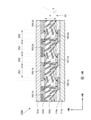
次に、図6を参照し、液晶光学素子10の一部の断面構造を説明する。
第1の透明電極181-1aは、隣り合う2つの第2の透明電極182-1a及び182-2aに挟まれる。第1の透明電極181-1aは、第4の透明電極184-1aにおける第3の透明電極183-2a側の端部、第4の透明電極184-1aと第3の透明電極183-2aと間のスペース、及び第3の透明電極183-2aにおける第4の透明電極184-1a側の端部と、z軸方向に沿って重畳する。
第1の透明電極181-1aと第2の透明電極182-1aとの間のスペースは、第4の透明電極184-1aと、z軸方向に沿って重畳する。第1の透明電極181-1aと第2の透明電極182-2aとの間のスペースは、第3の透明電極183-2aと、z軸方向に沿って重畳する。
第2の透明電極182-1aは、第3の透明電極183-1aにおける第4の透明電極184-1a側の端部、第3の透明電極183-1aと第4の透明電極184-1aとの間のスペース、及び第4の透明電極184-1aにおける第3の透明電極183-1a側の端部と、z軸方向に沿って重畳する。
第2の透明電極182-2aは、第2の透明電極182-1aと同様に構成される。
第3の透明電極183-2aは、隣り合う2つの第4の透明電極184-1a及び184-2aに挟まれる。第4の透明電極184-1aは、隣り合う2つの第3の透明電極183-1a及び183-2aに挟まれる。
第1の液晶セル110aは、複数の第1の領域ZN1、及び、複数の第2の領域ZN2を含む。複数の第1の領域ZN1、及び、複数の第2の領域ZN2は、x軸方向に沿って、交互に配置される。
第1の領域ZN1は、第2の領域ZN2と隣り合う。また、第1の領域ZN1は、z軸方向に沿って、第1の透明電極181-1aと第2の透明電極182-1aとの間のスペースが、第4の透明電極184-1aと重畳する領域を含む。さらに、第1の領域ZN1は、z軸方向に沿って、第1の透明電極181-1aと第2の透明電極182-2aとの間のスペースが、第3の透明電極183-2aと重畳する領域を含む。幅OV2は、z軸方向に沿って第1の透明電極181-1aが第4の透明電極184-1aにおける第3の透明電極183-2a側の端部と重畳する幅である。幅OV3は、z軸方向に沿って、第1の透明電極181-1aが第3の透明電極183-2aにおける第4の透明電極184-1a側の端部と重畳する幅である。
第2の領域ZN2は、z軸方向に沿って、第1の透明電極181-1aが、第4の透明電極184-1aにおける第3の透明電極183-2a側の端部と重畳する領域、第4の透明電極184-1aと第3の透明電極183-2aとの間のスペースと重畳する領域、及び、第1の透明電極181-1aが第3の透明電極183-2aにおける第4の透明電極184-1a側の端部と重畳する領域を含む。また、第2の領域ZN2は、z軸方向に沿って、第2の透明電極182-2aが、第3の透明電極183-2aにおける第4の透明電極184-2a側の端部と重畳する領域、第3の透明電極183-2aと第4の透明電極184-2aとの間のスペースと重畳する領域、及び、第4の透明電極184-2aにおける第3の透明電極183-2a側の端部と重畳する領域を含む。幅OV4は、z軸方向に沿って、第2の透明電極182-2aが第3の透明電極183-2aにおける第4の透明電極184-2a側の端部と重畳する幅である。幅OV1は、z軸方向に沿って、第2の透明電極182-1aが第4の透明電極184-1aにおける第3の透明電極183-1a側の端部と重畳する幅であってよく、z軸方向に沿って、第2の透明電極182-2aが第4の透明電極184-2aにおける第3の透明電極183-2a側の端部と重畳する幅であってもよい。
セルギャップdは、液晶層160aと第1の配向膜114aとが接する面と、液晶層160aと第1の配向膜114aとが接する面との間隔であってよく、第1の基板111aと第2の基板121aとの間隔であってもよい。例えば、照明装置100のセルギャップdは、液晶層160aと第1の配向膜114aとが接する面と、液晶層160aと第1の配向膜114aとが接する面との間隔である。
<1-4.液晶光学素子10による光の配光の制御>
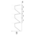
図7~図13を参照し、液晶光学素子10を用いた光の配光を説明する。図7は、図1に示されたA1-A2線に沿った第1の液晶セル110a及び第2の液晶セル110bの断面構造に対応するものである。図8及び図10は、液晶セルにおける液晶層の液晶の配向を示す断面図である。図9及び図11は、液晶セルにおける各領域と位相差の関係を示す図である。図12は、液晶光学素子10に含まれる各端子に供給する電圧を示すタイミングチャートである。図13は照明装置100における光の配光の方向を説明するための概略図である。図1~図6と同一、又は類似する構成は、必要に応じて説明する。
図7~図13を参照し、液晶光学素子10を用いた光の配光を説明する。図7は、図1に示されたA1-A2線に沿った第1の液晶セル110a及び第2の液晶セル110bの断面構造に対応するものである。図8及び図10は、液晶セルにおける液晶層の液晶の配向を示す断面図である。図9及び図11は、液晶セルにおける各領域と位相差の関係を示す図である。図12は、液晶光学素子10に含まれる各端子に供給する電圧を示すタイミングチャートである。図13は照明装置100における光の配光の方向を説明するための概略図である。図1~図6と同一、又は類似する構成は、必要に応じて説明する。
第1の液晶セル110aにおいて、第1の配向膜114aは、x軸方向に、かつ、端子部12から遠ざかる方向に配向処理されている(図4を参照)。第2の配向膜124aは、x軸方向に、かつ、端子部12に近づく方向に配向処理されている(図5を参照)。よって、第1の基板111a側の液晶分子の長軸、及び、第2の基板121a側の液晶分子の長軸は、x軸方向に配向する。第2の液晶セル110bの第1の配向膜114b、第2の配向膜124b及び液晶層160bの液晶分子は、第1の液晶セル110aと同様に構成されている。
はじめに、図7を参照し、第1の液晶セル110a及び第2の液晶セル110bの各透明電極に電位が供給されていない状態の液晶光学素子10を説明する。図7は、第1の透明電極181-1a及び181-1b、第2の透明電極182-1a、182-2a、182-1b及び182-2b、第3の透明電極183-1a、183-2a、183-1b及び183-2b、第4の透明電極184-1a、184-2a、184-1b及び184-2bに電位が供給されていない状態の液晶光学素子10を示す。図7では、接着層130a及び接着層130bは省略されている。
図7に示されるように、光源から出射された光は、x軸方向の偏光成分(P偏光成分)及びy軸方向の偏光成分(S偏光成分)を有するが、ここでは、便宜上、光をP偏光成分とS偏光成分とに分けて説明する。光源から出射された光(図7中の(1)を参照)は、P偏光成分を有する第1の偏光61及びS偏光成分を有する第2の偏光62を含む。図7中の矢印の記号及び丸印にバツを付した記号は、それぞれ、P偏光成分及びS偏光成分を表している。矢印はx軸に平行であることを表し、丸印にバツを付した記号はy軸に平行であることを表す。光源から出射された光は、液晶光学素子10に入射する光(入射光180)である。
第1の偏光61は、第1の基板111aに入射した後、P偏光成分を維持し、第2の基板121a側から出射される(図7中の(2)及び(3)を参照)。また、第1の偏光61は、波長板140に入射した後、第2の液晶セル110bに向かうにつれて、波長板140の位相差であるλ/2に基づき、P偏光成分からS偏光成分に変化する(図7中の(5)を参照)。さらに、第1の偏光61は、第1の基板111bに入射した後、S偏光成分を維持し、第2の基板121a側から出射される(図7中の(6)~(8)を参照)。
第2の偏光62は、第1の基板111aに入射した後、S偏光成分を維持し、第2の基板121a側から出射される(図7中の(2)及び(3)を参照)。また、第2の偏光62は、波長板140に入射した後、第2の液晶セル110bに向かうにつれて、波長板140の位相差であるλ/2に基づき、S偏光成分からP偏光成分に変化する(図7中の(5)を参照)。さらに、第2の偏光62は、第1の基板111bに入射した後、P偏光成分を維持し、第2の基板121a側から出射される(図7中の(5)~(8)を参照)。
液晶光学素子10は、同一の構造を有する2つの液晶セル(第1の液晶セル110a及び第2の液晶セル110b)を積層させた構造を有し、液晶光学素子10に入射する光の偏光成分を1度変化させる。その結果、液晶光学素子10は、入射前の偏光成分と入射後の偏光成分とを変えることができる(図7中の(1)~(8)参照)。すなわち、液晶光学素子10では、入射光180の偏光成分と、出射光の偏光成分とを90度回転することができる。
次に、図8~図13を参照し、第1の液晶セル110aの各透明電極に電位が供給された状態の液晶光学素子10を説明する。なお、第2の液晶セル110bの構成及び機能は第1の液晶セル110aの構成及び機能と同様であるから、必要に応じて説明される。
複数の第1の透明電極181及び複数の第2の透明電極182のうち、隣り合う第1の透明電極181と第2の透明電極182とに制御装置40から異なる制御信号(電位)が供給されると、隣り合う第1の透明電極181と第2の透明電極182との間で電位差が発生する。その結果、隣り合う第1の透明電極181と第2の透明電極182との間に電界(第1の電界)が発生する。第1の透明電極181及び第2の透明電極182と同様に、隣り合う第3の透明電極183と第4の透明電極184とに制御装置40から異なる制御信号(電位)が供給され、隣り合う第3の透明電極183と第4の透明電極184との間で電位差が発生すると、隣り合う第3の透明電極183と第4の透明電極184との間に電界(第2の電界)が発生する。例えば、第1の電界及び第2の電界は横電界と呼ばれる。
また、対向する第1の透明電極181と第3の透明電極183との間、及び、対向する第2の透明電極182と第4の透明電極184との間で電位差が発生する。その結果、対向する第1の透明電極181と第3の透明電極183との間、及び、対向する第2の透明電極182と第4の透明電極184との間に電界(第3の電界、第4の電界)が発生する。なお、対向する第1の透明電極181と第4の透明電極184との間、及び、対向する第2の透明電極182と第3の透明電極183との間には、同一の制御信号(電位)が供給されているため、電位差が発生しない。
例えば、図8及び図12に示されるように、第2の透明電極182-1a、第2の透明電極182-2a、第3の透明電極183-1a及び第3の透明電極183-2aにロー(Low)電位VLが供給され、第1の透明電極181-1a、第4の透明電極184-1a及び第4の透明電極184-2aにハイ(High)電位VHが供給される。その結果、第2の透明電極182-1aと第1の透明電極181-1aとの間には電位差(VH-VL)が発生し、横電界が発生する。その他の隣り合う電極間においても同様に、電位差(VH-VL)が発生し、横電界が発生する。例えば、ハイ電位VHはロー電位VLより大きく(高く)、ハイ電位VHはロー電位VLの極性を反転した電位である。また、中間(Mid)電位VMは、基準となる電位であり、グラウンドであってよく、0Vであってもよい。例えば、ハイ電位VHと中間電位VMとの電位差の絶対値は、ロー電位VLと中間電位との電位差の絶対値と同じである。
また、第2の透明電極182-1aと第4の透明電極184-1aとの間、第1の透明電極181-1aと第3の透明電極183-2aとの間、及び、第2の透明電極182-2aと第4の透明電極184-2aとの間に電位差(VH-VL)が発生し、電界が発生する。なお、第1の透明電極181-1aと第4の透明電極184-1aとの間、及び、第2の透明電極182-2aと第3の透明電極183-2aとの間では電位差が発生せず、電界は発生しない。
電界が発生すると、電界の影響を受けた液晶層160a内の液晶分子の配向状態が変化する。
はじめに、第1の領域ZN1の液晶分子の配向状態を説明する。第1の基板111a側の液晶分子の長軸が、第2の透明電極182-1aと第1の透明電極181-1aとの間の横電界に基づき、x軸方向に凸円弧状に配向する。また、第1の基板111aから第2の基板121aに向かうにつれて、液晶分子の長軸が、第2の透明電極182-1aと第4の透明電極184-1aとの間の電界に基づき、x軸方向からz軸方向に傾いて配向する。なお、液晶分子の長軸が、第4の透明電極184-1aと第3の透明電極183-2aとの間の横電界の影響を受けて、x軸方向からz軸方向に傾いて配向する場合もある。
また、第1の基板111a側の液晶分子の長軸が、第2の透明電極182-1aと第1の透明電極181-1aとの間の横電界に基づき、x軸方向に凸円弧状に配向する。さらに、第1の基板111aから第2の基板121aに向かうにつれて、液晶分子の長軸が、第2の透明電極182-1aと第4の透明電極184-1aとの間の電界に基づき、x軸方向からz軸方向に傾いて配向する。なお、液晶分子の長軸が、第4の透明電極184-1aと第3の透明電極183-2aとの間の横電界の影響を受けて、x軸方向からz軸方向に傾いて配向する場合もある。
その結果、例えば、第1の領域ZN1に入射する第1の偏光61は、第2の透明電極182-1aから第4の透明電極184-1aに向かって、制御角θで屈曲する。第1の領域ZN1に入射する第1の偏光61は、第1の透明電極181-1aから第3の透明電極183-2aに向かって、制御角θで屈曲する。例えば、制御角θは、断面視において、液晶分子の長軸と入射面63とがなす角である。
次に、第2の領域ZN2の液晶分子の配向状態を説明する。例えば、第1の透明電極181-1aと第4の透明電極184-1aとの間には電界が発生しないため、液晶分子の長軸が、x軸に沿って平行に配向する。実際は、液晶分子の長軸が、第2の透明電極182-1aと第1の透明電極181-1aとの間の横電界、及び、第4の透明電極184-1aと第3の透明電極183-2aとの間の横電界の影響を受けて、x軸方向からz軸方向に傾いて配向する場合もある。また、液晶分子の長軸は、第1の透明電極181-1aと第3の透明電極183-2aとの間の電界に基づき、z軸方向に沿って配向する。なお、液晶分子の長軸は、第4の透明電極184-1aと第3の透明電極183-2aとの間の横電界の影響を受けて、z軸方向からx軸方向に傾く場合もある。その結果、例えば、第2の領域ZN2に入射する第1の偏光61は、第2の透明電極182-1aから第4の透明電極184-1aに向かって、概ね直進し、z軸方向からx軸方向に傾く場合もある。
また、例えば、第2の透明電極182-1aと第3の透明電極183-2aとの間には電界が発生しないため、液晶分子の長軸が、x軸に沿って平行に配向する。実際は、液晶分子の長軸が、第2の透明電極182-2aと第1の透明電極181-1aとの間の横電界、及び、第4の透明電極184-2aと第3の透明電極183-2aとの間の横電界の影響を受けて、x軸方向からz軸方向に傾いて配向する場合もある。また、液晶分子の長軸は、第2の透明電極182-2aと第4の透明電極184-2aとの間の電界に基づき、z軸方向に沿って配向する。なお、液晶分子の長軸は、第4の透明電極184-1aと第3の透明電極183-2aとの間の横電界の影響を受けて、z軸方向からx軸方向に傾く場合もある。その結果、例えば、第2の領域ZN2に入射する第1の偏光61は、第2の透明電極182-2aから第4の透明電極184-2aに向かって、概ね直進し、z軸方向からx軸方向に傾く場合もある。
図8に示された各領域における液晶の配向は、各領域と位相差の関係として、図9のように示すことができる。本明細書及び図面において、位相差は、セルギャップd及び係数Δnを用いて、セルギャップdと係数Δnとの積、すなわち、Δndで表される。また、制御角θは、各電極に供給される電位に応じて、調整することができる。例えば、図8及び図9における制御角θは、90度より小さい。
図9に示されるように、第1の領域ZN1に入射した光は、第1の基板111a側から第2の基板121a側に向かうにつれて、位相差が徐々に増加する。位相差が増加することは、光が第1の基板111a側から第2の基板121a側に出射されることを意味する。すなわち、第1の領域ZN1に入射した光は、第1の基板111a側から第2の基板121a側に向かうにつれて屈曲し、第2の基板121aから出射される。また、第2の領域ZN2に入射した光は、第1の基板111a側から第2の基板121a側に向かうにつれて、位相差がわずかに上昇した後に減少する。位相差が減少することは、光が、第2の基板121a側から第1の基板111a側に向かうと共に、第2の基板121aから出射されないことを意味する。すなわち、第2の領域ZN2に入射した光は、第2の基板121aから出射されない。
図8及び図9に示されるように、照明装置100の各電極にハイ電位VH又はロー電位VLが供給されることによって、照明装置100は、第1の液晶セル110aの入射面63に入射した光(例えば、入射光180(図1を参照))を、制御角θで屈曲させて、第1の液晶セル110aから出射させることができる。また、図13に模式的に示すように、第1の液晶セル110aから出射された屈曲した光は、波長板140及び第2の液晶セル110bを透過し、第2の液晶セル110bから出射される。第1の液晶セル110aの入射面63に入射した第1の偏光61は屈曲し、波長板140で90度回転されたのちに、第2の液晶セル110bを透過して、液晶光学素子10から出射される。第2の偏光62は、第1の偏光61と90度回転しているため、第1の液晶セル110a内を透過し、波長板140で90度回転されたのちに、第2の液晶セル110bで第1の偏光61と同様に屈曲されて、液晶光学素子10から出射される。なお、図13に示される図は、照明装置100を模式的に示した図であり、実際は、第1の偏光61及び第2の偏光62は、90度回転する。
例えば、セルギャップdが30μm、第1の電極間距離p1が35μm、及び、Δnが0.2の条件において、ハイ電位VH及びロー電位VLを設定した場合には、制御角θが10度となる。すなわち、当該条件の下では、照明装置100は、第1の液晶セル110aの入射面63に入射した光を、10度の角度で屈曲させて、第1の液晶セル110aから出射させることができる。さらに、照明装置100は、第1の液晶セル110aから出射した10度の角度で屈曲した光を、波長板140で90度回転させたのちに、第2の液晶セル110bを透過させて、液晶光学素子10(第2の液晶セル110b)から出射させることができる。また、照明装置100は、第1の液晶セル110aの入射面63に入射した光を第1の液晶セル110a内を透過させて第1の液晶セル110aから出射させることができる。さらに、照明装置100は、第1の液晶セル110aから出射した光を、波長板140で90度回転させたのちに、第2の液晶セル110bで10度の角度で屈曲させて、液晶光学素子10(第2の液晶セル110b)から出射させることができる。
また、例えば、図10及び図12に示されるように、第2の透明電極182-1a、第2の透明電極182-2a、第4の透明電極184-1a及び第4の透明電極184-2aにハイ電位VH(+)が供給され、第1の透明電極181-1a、第3の透明電極183-1a及び第3の透明電極183-2aにロー電位VL(-)が供給される。その結果、第2の透明電極182-1aと第1の透明電極181-1aとの間には電位差(VH-VL)が発生し、横電界が発生する。その他の隣り合う電極間においても同様に、電位差(VH-VL)が発生し、横電界が発生する。
また、第2の透明電極182-1aと第4の透明電極184-1aとの間、第1の透明電極181-1aと第3の透明電極183-2aとの間、及び、第2の透明電極182-2aと第4の透明電極184-2aとの間に電位差(VH-VL)が発生し、電界が発生する。なお、第2の透明電極182-1aと第3の透明電極183-1aとの間、第1の透明電極181-1aと第4の透明電極184-1aとの間、及び、第2の透明電極182-2aと第3の透明電極183-2aとの間では電位差が発生せず、電界は発生しない。
電界が発生すると、電界の影響を受けた液晶層160a内の液晶分子の配向状態が変化する。
図10で示された構成は、図8で示された構成と、第2の透明電極182-1a、第2の透明電極182-2a及び第1の透明電極181-1aに供給される電位の極性が反転している。よって、図10で示された構成の各領域で液晶分子が配向する方向は、図8で示された構成の各領域で液晶分子が配向する方向と、z軸方向に対称な方向である。以下において、図10で示された構成の各領域で液晶分子が配向する方向の一例を説明するが、以下で説明のない図10で示された構成の各領域で液晶分子が配向する方向は、図8で示された構成の各領域で液晶分子が配向する方向と、z軸方向に対称な方向である。
例えば、第1の領域ZN1の液晶分子の配向状態を説明する。第1の基板111a側の液晶分子の長軸が、第2の透明電極182-1aと第1の透明電極181-1aとの間の横電界に基づき、x軸方向に凸円弧状に配向する。また、第1の基板111aから第2の基板121aに向かうにつれて、液晶分子の長軸が、第1の透明電極181-1aと第4の透明電極184-1aとの間の電界に基づき、x軸方向からz軸方向に傾いて配向する。なお、液晶分子の長軸が、第4の透明電極184-1aと第3の透明電極183-1aとの間の横電界の影響を受けて、x軸方向からz軸方向に傾いて配向する場合もある。
その結果、例えば、第1の領域ZN1に入射する第1の偏光61は、第1の透明電極181-1aから第4の透明電極184-1aに向かって、制御角θで屈曲する。また、第1の領域ZN1に入射する第1の偏光61は、第2の透明電極182-3aから第3の透明電極183-2aに向かって、制御角θで屈曲する。
例えば、第2の領域ZN2の液晶分子の配向状態を説明する。第1の透明電極181-1aと第3の透明電極183-2aとの間には電界が発生しないため、液晶分子の長軸が、x軸に沿って平行に配向する。実際は、液晶分子の長軸が、第2の透明電極182-2aと第1の透明電極181-1aとの間の横電界、及び、第4の透明電極184-1aと第3の透明電極183-2aとの間の横電界の影響を受けて、x軸方向からz軸方向に傾いて配向する場合もある。また、液晶分子の長軸は、第1の透明電極181-1aと第4の透明電極184-1aとの間の電界に基づき、z軸方向に沿って配向する。なお、液晶分子の長軸は、第4の透明電極184-1aと第3の透明電極183-2aとの間の横電界の影響を受けて、z軸方向からx軸方向に傾く場合もある。その結果、例えば、第2の領域ZN2に入射する第1の偏光61は、第1の透明電極181-1aから第4の透明電極184-1aに向かって、概ね直進し、z軸方向からx軸方向に傾く場合もある。また、例えば、複数の第1の透明電極181及び複数の第2の透明電極182を形成する材料は、透明な材料でなく、不透明な材料であってよく、アルミニウム、モリブデンなどの金属材料であってよい。この場合、第2の領域ZN2に入射する第1の偏光61は、第1の透明電極181-1a側から第4の透明電極184-1a側に向かって、概ね直進するため、屈曲した光のみ出射される。
図10に示された各領域における液晶の配向は、各領域と位相差の関係として、図11のように示すことができる。図10で示された構成の各領域で液晶分子が配向する方向は、図8で示された構成の各領域で液晶分子が配向する方向と、z軸方向に対称な方向である。よって、図11に示された各領域と位相差の関係は、図9に示された各領域と位相差の関係と、直線の傾きが反転している。すなわち、図9に示された第1の領域ZN1では、第1の領域ZN1から第2の領域ZN2に近づくほど、位相差は増加するのに対し、図11に示された第1の領域ZN1では、第2の領域ZN2から第1の領域ZN1に近づくほど、位相差は増加する。図11に示された第2の領域の位相差は、図11に示された第1の領域ZN1の位相差と同様に、図9に示された第2の領域の位相差と、直線の傾きが反転している。
すなわち、図10及び図11に示された構成は、図8及び図9に示された構成とx軸方向に反対の向きに、光を屈曲する構成である。例えば、図8で示された構成における制御角θは90度より小さいが、図10で示された構成における制御角θは90度より大きい。例えば、図10で示された構成の照明装置100は、図8で示された構成の照明装置100が右方向に光を屈曲させる条件を用いることによって、左方向に光を屈曲させることができる。
以上説明したとおり、照明装置100は、制御角θで屈曲した光を、液晶光学素子10から出射させることができる。また、照明装置100は、液晶光学素子10に含まれる各電極に電位を供給することによって、供給された電位に応じた制御角θで屈曲した光を、液晶光学素子10から出射させることができる。よって、照明装置100は、液晶光学素子10を用いて、光の配光方向及び光の配光角を調整することが可能であると共に、調整された様々な配光方向及び配光角を有する光を照射することができる。
<1-5.光源30の構成>
図14及び図15は光源30を示す概略図である。例えば、図14に示されるように、光源30は、発光素子31及び反射器32を含んでよく、図15に示されるように、光源30は、発光素子31及び凸レンズ33を含んでもよい。なお、光源の構成及び機能は、光源30の構成及び機能に限定されない。例えば、光源30は、光の配光を狭角に可能な構成であってもよい。
図14及び図15は光源30を示す概略図である。例えば、図14に示されるように、光源30は、発光素子31及び反射器32を含んでよく、図15に示されるように、光源30は、発光素子31及び凸レンズ33を含んでもよい。なお、光源の構成及び機能は、光源30の構成及び機能に限定されない。例えば、光源30は、光の配光を狭角に可能な構成であってもよい。
例えば、発光素子31はLEDである。反射器32は、発光素子31から出射された光を反射し、反射した光を液晶光学素子10に向けて出射することができる。図15に示される反射器32の形状は、略円錐形であるが、反射器32の形状は略円錐形に限定されない。また、反射器32の表面は平面であってよく、曲面であってもよい。凸レンズ33は、発光素子31から出射された光を集光し、集光した光を液晶光学素子10に向けて出射することができる。
<第2実施形態>
図16~図25を参照し、第2実施形態に係る照明装置200の構成の概略を説明する。図16は照明装置200の構成を示す模式的な斜視図である。照明装置200は、照明装置100と比較して、波長板140を含まず、第1の基板上の各電極の構成、第2の基板上の各電極の構成が異なる。照明装置200のその他の構成は、照明装置100の構成と同様である。よって、照明装置100と同様の構成は、必要に応じて、説明する。また、図1~図15と同一、又は類似する構成は、必要に応じて説明する。
図16~図25を参照し、第2実施形態に係る照明装置200の構成の概略を説明する。図16は照明装置200の構成を示す模式的な斜視図である。照明装置200は、照明装置100と比較して、波長板140を含まず、第1の基板上の各電極の構成、第2の基板上の各電極の構成が異なる。照明装置200のその他の構成は、照明装置100の構成と同様である。よって、照明装置100と同様の構成は、必要に応じて、説明する。また、図1~図15と同一、又は類似する構成は、必要に応じて説明する。
<2-1.照明装置200の構成>
図16を参照し、照明装置200の構成の概略を説明する。図16は照明装置200の構成を示す模式的な斜視図である。
図16を参照し、照明装置200の構成の概略を説明する。図16は照明装置200の構成を示す模式的な斜視図である。
図16に示されるように、照明装置200は、液晶光学素子20、光源30、及び制御装置40を含む。詳細は後述するが、液晶光学素子20は、第1の液晶セル210a、接着層230a、及び第2の液晶セル210bを含む。接着層230aは第1の液晶セル210aと第2の液晶セル210bとの間に設けられる。第1の液晶セル210a、接着層230a、及び第2の液晶セル210bは、z軸方向に沿って、光源に近い方からこの順に位置するように積層されている。
第1の液晶セル210a及び第2の液晶セル210bの基本的な構成及び機能は同じである。よって、第1の液晶セル210a及び第2の液晶セル210bが区別されない場合には、液晶セルは液晶セル210として説明され、第1の液晶セル210a及び第2の液晶セル210bが区別される場合には、液晶セルは第1の液晶セル210a及び第2の液晶セル210bとして説明される。
接着層230aは、第1の液晶セル210a及び第2の液晶セル210bを接着し、固定する。接着層230aを形成する材料は、接着層130aと同様の材料を用いることができる。
光源30及び制御装置40は、照明装置100と同様の構成を有する。制御装置40は、液晶光学素子20及び光源30を制御する。具体的には、制御装置40は、液晶光学素子20の第1の液晶セル210a及び第2の液晶セル210bに、光の配光方向及び配向角を制御可能な制御信号(電位)を供給し、光源30の点灯及び明るさを制御可能な制御信号(電位)を供給することができる。
液晶光学素子20及び光源30は、制御装置40と電気的に接続されている。例えば、制御装置40は、液晶光学素子20の及び第2の液晶セル210bと電気的に接続されている。制御装置40は、第1の液晶セル210aの端子部22aに電気的に接続された第1のフレキシブル配線基板11a及び第2の液晶セル210bの端子部22bに電気的に接続された第2のフレキシブル配線基板11bを介して電気的に接続される。
光源30から液晶光学素子20に出射された光は、第1の液晶セル210a、接着層230a、及び第2の液晶セル210bを透過し、第2の液晶セル210bから出射される。詳細は後述されるが、例えば、液晶光学素子20を透過する光は、液晶セル210に含まれる各電極の構成、及び、制御装置40から各電極に供給される電圧に基づき、x軸方向又はy軸方向に屈折する。すなわち、照明装置200は、液晶光学素子20を用いて光の配光方向及び光の配光角を調整することが可能であると共に、調整された様々な配光方向及び配光角を有する光を照射することができる。
<2-2.液晶光学素子20の構成>
図17及び図18を参照し、液晶光学素子20の構成の概略を説明する。図17及び図18は、液晶光学素子20の一部の断面構造を示す模式的な断面図である。具体的には、図17は、図16に示されるC1-C2線に沿って切断されたzx面内の模式的な断面図であり、図18は、図16に示されるD1-D2線に沿って切断されたyz面内の模式的な断面図である。また、図16と同一、又は類似する構成は、必要に応じて説明する。以降の説明では、第1の液晶セル210aの構成及び機能が説明され、必要に応じて、第2の液晶セル210bの構成及び機能が説明される。
図17及び図18を参照し、液晶光学素子20の構成の概略を説明する。図17及び図18は、液晶光学素子20の一部の断面構造を示す模式的な断面図である。具体的には、図17は、図16に示されるC1-C2線に沿って切断されたzx面内の模式的な断面図であり、図18は、図16に示されるD1-D2線に沿って切断されたyz面内の模式的な断面図である。また、図16と同一、又は類似する構成は、必要に応じて説明する。以降の説明では、第1の液晶セル210aの構成及び機能が説明され、必要に応じて、第2の液晶セル210bの構成及び機能が説明される。
第1の液晶セル210aは、第1の基板211a、第2の基板221a、複数の第1の透明電極281(例えば、第1の透明電極281-1a、第1の透明電極281-2a)、複数の第2の透明電極282(例えば、第2の透明電極282-1a、第2の透明電極282-2a、第2の透明電極282-3a)、複数の第3の電極283(例えば、第3の電極283-1a、第3の電極283-2a、第3の電極283-3a)、第4の透明電極284、第1の配向膜214a、第2の配向膜224a、及び液晶層260aを含む。
第1の基板211a、第2の基板221a、複数の第1の透明電極281、複数の第2の透明電極282、第1の配向膜214a、第2の配向膜224a、及び液晶層260aのそれぞれの構成は、第1の基板111a、第2の基板121a、複数の第1の透明電極181、複数の第2の透明電極182、第1の配向膜114a、第2の配向膜124a、及び液晶層160aのそれぞれの構成と同様である。よって、第1の基板211a、第2の基板221a、複数の第1の透明電極281、複数の第2の透明電極282、第1の配向膜214a、第2の配向膜224a、及び液晶層260aの構成は、必要に応じて説明する。
複数の第3の電極283は第2の基板221aの上に配置される。複数の第3の電極283は、光を遮る遮光膜として機能する。第4の透明電極284は、複数の第3の電極283、及び、第2の基板221aを覆うように、複数の第3の電極283、及び、第2の基板221aの上に接するように配置される。第1の基板211aの上の第1の透明電極281及び第2の透明電極282は、第2の基板221aの上の第3の電極283及び第4の透明電極284と対向するように配置される。
なお、照明装置100と同様に、照明装置200の第1の基板211a及び第2の基板221aは、シール材(図示は省略)を用いて接着され、照明装置200の液晶を含む液晶層260aは、第1の配向膜214a、第2の配向膜224a、及びシール材で囲まれた空間に設けられている。
複数の第1の透明電極281、複数の第2の透明電極282、複数の第3の電極283のそれぞれは、y軸方向に延在する。複数の第3の電極283は、x軸方向に沿って、間隔を空けて配置される。
複数の第1の透明電極281、複数の第2の透明電極282、及び、複数の第3の電極283と同様に、第4の透明電極284は、液晶層260aに電界を形成するための電極として機能する。複数の第1の透明電極281、複数の第2の透明電極282、及び第4の透明電極284として、例えば、インジウム・スズ酸化物(ITO)またはインジウム・亜鉛酸化物(IZO)などの透明導電材料が用いられる。
第1の液晶セル210aの第1の基板211a側の液晶分子の配向方向は、複数の第1の透明電極281及び複数の第2の透明電極282の延在方向と直交する方向となるように、第1の配向膜214aに配向特性が付与される。例えば、第1の透明電極281及び第2の透明電極282の長軸の方向が配向処理の方向x軸方向と直交することによって、配向処理の方向と、第1の透明電極281と第2の透明電極282との間に電位差が発生した場合の電界の方向とが一致する。その結果、液晶光学素子10は、光の取り出し効率が良い。
また、第1の液晶セル210aの第2の基板221a側の液・BR>サ分子の配向方向は、複数の第3の電極283の延在方向と平行な方向となるように、第2の配向膜224aに配向特性が付与される。
図17及び図18には、便宜上、矢印及び丸印の中にバツを付した記号を用いて、液晶層260a内の液晶分子の配向方向が示されている。矢印は、紙面と平行方向に配向する液晶分子の配向方向を表し、丸印の中にバツを付した記号は、紙面と垂直方向に配向する液晶分子の配向方向を表す。例えば、第1の基板211a側の液晶分子の配向方向はx軸方向であり、第2の基板221a側の液晶分子の配向方向はy軸方向である。
図17に示されるように、液晶光学素子20のx軸方向の断面構造の液晶分子は、第1の基板211a側から第2の基板221a側に向かうにつれて、液晶分子の配向方向がx軸方向からy軸方向に変化し、90度捩れるように配向する。
図18に示されるように、液晶光学素子20のx軸方向の断面構造の液晶分子は、第1の基板211a側から第2の基板221a側に向かうにつれて、液晶分子の配向方向がy軸方向からx軸方向に変化し、90度捩れるように配向する。なお、図17及び図18は、第1の液晶セル210a及び第2の液晶セル210bの各透明電極に電位が供給されていない状態の液晶光学素子20の状態である。
第2の液晶セル210bは、第1の基板211b、第2の基板221b、複数の第1の透明電極281(例えば、第1の透明電極281-1b、第1の透明電極281-2b)、複数の第2の透明電極282(例えば、第2の透明電極282-1b、第2の透明電極282-2b、第2の透明電極282-3b)、複数の第3の電極283(例えば、第3の電極283-1b、第3の電極283-2b、第3の電極283-3b)、第4の透明電極284、第1の配向膜214b、第2の配向膜224b、及び液晶層260bを含む。第1の基板211b、第2の基板221b、複数の第1の透明電極281、複数の第2の透明電極282、複数の第3の電極283、第4の透明電極284、第1の配向膜214b、第2の配向膜224b、及び液晶層260bは、それぞれ、第1の基板211a、第2の基板221a、複数の第1の透明電極281、複数の第2の透明電極282、複数の第3の電極283、第4の透明電極284、第1の配向膜214a、第2の配向膜224a、及び液晶層260aと同様の構成及び機能を有する。よって、ここでの第2の液晶セル210bの説明は省略される。
平面視において、第1の液晶セル210a及び第2の液晶セル210bに設けられる第1の透明電極281同士の延在する方向(y軸方向)は互いに一致するように重畳している。第1の液晶セル210a及び第2の液晶セル210bに設けられる同一名の透明電極も同様に、延在する方向(y軸方向)は互いに一致するように重畳している。すなわち、照明装置200は、同じ構成の液晶セル(第1の液晶セル210a及び第2の液晶セル210b)が重畳した構成を含む。なお、図17及び図18に示されるように、第1の液晶セル210a及び第2の液晶セル210bを構成する上下一対の基板のうち、下側の基板(光源側の基板)が第1の基板211a及び第1の基板211bとなっている。
「1-1.照明装置200の構成」で説明したとおり、第1の液晶セル210a及び第2の液晶セル210bの基本的な構成及び機能は同じである。よって、第1の基板211a及び第1の基板211b、第2の基板221a及び第2の基板221b、複数の第1の透明電極281、複数の第2の透明電極282、複数の第3の電極283、第4の透明電極284、第1の配向膜214a及び第1の配向膜214b、第2の配向膜224a及び第2の配向膜224b、液晶層260a及び液晶層260bのそれぞれが、区別される場合には、各名称を用いて説明される。上述の第1の液晶セル210a及び第2の液晶セル210bに含まれる各構成要素のそれぞれが区別されない場合には、第1の液晶セル210a及び第2の液晶セル210bに含まれる各構成要素のそれぞれは、第1の基板211、第2の基板221、複数の第1の透明電極281、複数の第2の透明電極282、複数の第3の電極283、複数の第4の透明電極284、第1の配向膜214、第2の配向膜224、液晶層260として説明される。
<2-3.透明電極の配置>
図16、図19~図21を参照し、液晶光学素子20の各電極の概略を説明する。図19は、液晶光学素子20の第1の基板211上の複数の第1の透明電極281及び複数の第2の透明電極282の配置を示す模式的な平面図である。図20は、液晶光学素子20の第2の基板221上の複数の第3の電極283及び第4の透明電極284の配置を示す模式的な平面図である。図21は、液晶光学素子20の一部の断面構造を示す断面図である。なお、図21は図16に示されたC1-C2線に沿った第1の液晶セル210aの断面構造に対応するものである。図16~図18と同一、又は類似する構成は、必要に応じて説明する。
図16、図19~図21を参照し、液晶光学素子20の各電極の概略を説明する。図19は、液晶光学素子20の第1の基板211上の複数の第1の透明電極281及び複数の第2の透明電極282の配置を示す模式的な平面図である。図20は、液晶光学素子20の第2の基板221上の複数の第3の電極283及び第4の透明電極284の配置を示す模式的な平面図である。図21は、液晶光学素子20の一部の断面構造を示す断面図である。なお、図21は図16に示されたC1-C2線に沿った第1の液晶セル210aの断面構造に対応するものである。図16~図18と同一、又は類似する構成は、必要に応じて説明する。
第1の液晶セル210aの断面構造は第2の液晶セル210bの断面構造と同じであり、第1の液晶セル210aの断面構造がここでは説明され、第2の液晶セル210bの断面構造は必要に応じて説明される。
はじめに、図16、図19及び図20を参照し、平面視における液晶光学素子20の各電極の概略を説明する。図19に示されるように、平面視において、複数の第1の透明電極281、複数の第2の透明電極282、第1の端子219-1、及び第2の端子219-2が第1の基板211上に設けられる。また、第5の配線216-5、第6の配線216-6、複数の第1の給電端子218-1、複数の第2の給電端子218-2、及び第3の端子219-3が第1の基板211上に設けられる。
複数の第1の透明電極281及び複数の第2の透明電極282は、制御装置40から制御信号(電位)を供給され、光源30から出射される光を、透過する機能、透過しにくくする機能、拡散する機能、及び屈折する機能を有する。
複数の第1の透明電極281は第1の透明電極281-1を含む。複数の第2の透明電極282は第2の透明電極282-1及び第2の透明電極282-2を含む。複数の第1の透明電極281及び複数の第2の透明電極282のそれぞれの長軸がy軸方向に延在し、第1の透明電極281及び第2の透明電極282はx軸方向に沿って交互に配置される。
第1の透明電極281の電極の幅、及び第2の透明電極282の電極の幅(x軸方向の幅)は、第3の幅w3である。第1の透明電極281と第2の透明電極282とのx軸方向の電極間距離(電極間隔)は、第3の電極間距離p3である。照明装置200において、第3の幅w3は第3の電極間距離p3と異なる。第1の透明電極281の電極の幅と第2の透明電極282の電極の幅は異なっていてもよい。
また、セルギャップdは、第3の電極間距離p3より小さい(狭い)。例えば、照明装置200のセルギャップdは、照明装置100のセルギャップdと同様の構成を有する。例えば、照明装置200のセルギャップdは30μmである。セルギャップdが第3の電極間距離p3より(狭い)小さいことに基づき、第1の基板211a側及び第2の基板112a側で発生した横電界は、第1の基板211aと第2の基板112aとの間の中央近傍に位置する液晶分子に影響を及ぼし、照明装置200は入射光180を屈曲させることができる。
複数の第1の透明電極281は第1の配線216-1と電気的に接続され、第1の配線216-1は第1の端子219-1と電気的に接続される。第1の配線216-1は、複数の第1の透明電極281の下に形成されてよく、複数の第1の透明電極281の上に形成されてもよい。また、第1の配線216-1は、複数の第1の透明電極281と同じ層に形成されてもよい。複数の第2の透明電極282は第2の配線216-2と電気的に接続され、第2の配線216-2は第2の端子219-2と電気的に接続される。第2の配線216-2は、複数の第2の透明電極282の下に形成されてよく、複数の第2の透明電極282の上に形成されてもよい。また、第2の配線216-2は、複数の第2の透明電極282と同じ層に形成されてもよい。例えば、照明装置200の複数の第1の透明電極281及び複数の第2の透明電極282は、第1の配線216-1及び第2の配線216-2と同じ層に形成されている。
第5の配線216-5は、複数の第1の給電端子218-1、第6の配線216-6、複数の第2の給電端子218-2、及び第3の端子219-3に電気的に接続される。
第1の基板211上に配置される第1の配向膜214は、x軸方向(図19において白抜きの矢印で示す方向)に配向処理されている。この場合、液晶層260を構成する液晶分子のうち、第1の基板211側の液晶分子の長軸は、x軸方向に沿って配向する。すなわち、第1の配向膜214の配向方向(x軸方向)と複数の第1の透明電極281及び複数の第2の透明電極282の延在する方向(y軸方向)は直交している。
図20に示されるように、平面視において、複数の第3の電極283、第4の透明電極284、複数の第3の給電端子218-3、及び複数の第4の給電端子218-4が第2の基板221上に設けられる。複数の第3の電極283、複数の第3の給電端子218-3、及び複数の第4の給電端子218-4は、第2の基板221と第4の透明電極284との間に形成されてよく、第2の基板221の上に形成された第4の透明電極284の上に形成されてもよい。例えば、複数の第3の電極283、第4の透明電極284、複数の第3の給電端子218-3、及び複数の第4の給電端子218-4は第2の基板221の上に形成され、第2の基板221と第4の透明電極284との間に形成されている。また、複数の第3の電極283、第4の透明電極284、複数の第3の給電端子218-3、及び複数の第4の給電端子218-4は、第4の透明電極284に覆われ、第4の透明電極284と接している。複数の第3の電極283、及び複数の第3の給電端子218-3は、第4の透明電極284と電気的に接続される。
複数の第3の電極283及び第4の透明電極284は、複数の第1の透明電極281及び複数の第2の透明電極282と同様に、制御装置40から制御信号(電位)を供給され、光源30から出射される光を、透過する機能、透過しにくくする機能、拡散する機能、及び屈折する機能を有する。
複数の第3の電極283は第3の電極283-1、第3の電極283-2及び第3の電極283-3を含む。複数の第3の電極283のそれぞれの長軸が、y軸方向に延在し、第3の電極283はx軸方向に沿って間隔を空けて配置される。第3の電極283の電極の幅は、第4の幅w4である。隣り合う第3の電極283のx軸方向の電極間距離(電極間隔)は、第4の電極間距離p4である。照明装置200において、第4の幅w4は、第3の幅w3より広く(太く)、第3の電極間距離p3は第4の電極間距離p4より狭い(細い)。セルギャップdは、第4の幅w4より狭い。
液晶セル210において、複数の第1の透明電極281及び複数の第2の透明電極282と、複数の第3の電極283及び第4の透明電極284とは、液晶層260aを介して対向している。また、複数の第1の透明電極281、及び複数の第2の透明電極282の延在する方向(y軸方向)は、複数の第3の電極283の延在する方向(y軸方向)と平行である。
第1の基板211が第2の基板221と貼り合わされると、複数の第1の給電端子218-1のそれぞれは、対応する第3の給電端子218-3に電気的に接続され、複数の第2の給電端子218-2のそれぞれは、対応する第4の給電端子218-4に電気的に接続される。その結果、第1の配線216-1及び第6の配線216-6は、複数の第3の電極283及び第4の透明電極284に電気的に接続される。例えば、第1の給電端子218-1と第3の給電端子218-3、及び、第2の給電端子218-2と第4の給電端子218-4は、銀ペースト又は導電粒子を用いて、電気的に接続することができる。なお、導電粒子は金属を被覆した粒子を含む。
例えば、図16、図19及び図20に示されるように、第2の基板221のx軸方向に沿った長さは、第1の基板211のx軸方向に沿った長さより短い。第1の端子219-1、第2の端子219-2、及び第3の端子219-3は、第1の基板211上の端子部22に設けられる。その結果、第1の基板211が第2の基板221と貼り合わされると、第1の端子219-1、第2の端子219-2及び第3の端子219-3は、第2の基板221に覆われずに露出される。
よって、第1の液晶セル210aにおいて、端子部22aは第1のフレキシブル配線基板11aと容易に貼り合わせることができ、容易に電気的に接続することができる。その結果、複数の第1の透明電極281は、第1のフレキシブル配線基板11a、端子部22a、第1の端子219-1、第1の配線216-1を介して、制御装置40(図16を参照)から制御信号(電位)を供給される。複数の第2の透明電極282は、第1のフレキシブル配線基板11a、端子部22a、第2の端子219-2、第2の配線216-2を介して、制御装置40から制御信号(電位)を供給される。複数の第3の電極283及び第4の透明電極284は、第1のフレキシブル配線基板11a、端子部22a、第3の端子219-3、第5の配線216-5、複数の第1の給電端子218-1、第6の配線216-6、複数の第2の給電端子218-2、複数の第3の給電端子218-3、複数の第4の給電端子218-4を介して、制御装置40から制御信号(電位)を供給される。第1の液晶セル210aと同様に、第2の液晶セル210bの端子部22bも、第2のフレキシブル配線基板11bと容易に貼り合わせることができ、容易に電気的に接続することができる。また、第1の液晶セル210aと同様に、第2の液晶セル210b内の各電極も制御装置40から制御信号(電位)を供給される。
第1の配線216-1、第2の配線216-2、第5の配線216-5、第6の配線216-6、複数の第1の給電端子218-1、複数の第3の給電端子218-3、複数の第2の給電端子218-2、複数の第4の給電端子218-4、第1の端子219-1、第2の端子219-2、第3の端子219-3、及び複数の第3の電極283を形成する材料として、金属材料を用いることができる。金属材料は、例えば、アルミニウム、モリブデンである。
次に、図21を参照し、液晶光学素子20の一部の断面構造を説明する。
第1の透明電極281-1aは、隣り合う2つの第2の透明電極282-1a及び282-2aに挟まれる。第1の透明電極281-1aは、第3の電極283-2aにおける第3の電極283-1a側の端部、及び、第3の電極283-1aと第3の電極283-2aと間のスペースと、z軸方向に沿って重畳する。
第1の透明電極281-1aと第2の透明電極282-1aとの間のスペースは、第3の電極283-1aと第3の電極283-2aと間のスペースと、z軸方向に沿って重畳する。
第2の透明電極282-1aは、第3の電極283-1aにおける第3の電極283-2a側の端部、及び、第3の電極283-1aと第3の電極283-2aとの間のスペースと、z軸方向に沿って重畳する。
第1の透明電極281-2aは第1の透明電極281-1aと同様に構成される。第2の透明電極282-2a及び第2の透明電極282-3aは、第2の透明電極282-1aと同様に構成される。
第3の電極283-2aは、隣り合う2つの第3の電極283-1a及び第3の透明電極183-3aに挟まれる。第3の電極283-1aと第3の電極283-2aとの間、第3の電極283-2aと第3の電極283-3aとの間、第3の電極283-1aの上面、第3の電極283-2aの上面、及び第3の電極283-3aの上面は、第4の透明電極284が配置される。
第1の液晶セル210aは、複数の第1の領域ZN1、及び、複数の第2の領域ZN2を含む。複数の第1の領域ZN1、及び、複数の第2の領域ZN2は、x軸方向に沿って、交互に配置される。
第1の領域ZN1は、第2の領域ZN2と隣り合う。また、第1の領域ZN1は、z軸方向に沿って、第1の透明電極281-1aと第2の透明電極282-1aとの間のスペースが第3の電極283-1aと第3の電極283-2aとの間のスペースと重畳する領域、第3の電極283-1aと第3の電極283-2aと間のスペースが第1の透明電極281-1aにおける第2の透明電極282-1a側の端部と重畳する領域、第3の電極283-1aと第3の電極283-2aと間のスペースが第2の透明電極282-1aにおける第1の透明電極281-1a側の端部と重畳する領域を含む。すなわち、第1の領域ZN1は、z軸方向に沿って、第1の透明電極281と第2の透明電極282との間のスペースが、隣り合う第3の電極283の間のスペースと重畳する領域、隣り合う第3の電極283の間のスペースが第1の透明電極281の端部と重畳する領域、隣り合う第3の電極283の間のスペースが第2の透明電極282の端部と重畳する領域を含む。
第2の領域ZN2は、z軸方向に沿って、第1の透明電極281-1aと第2の透明電極282-2aとの間のスペースが、対向する第3の電極283-2aと重畳する領域、第1の透明電極281-1aにおける第2の透明電極282-2a側の端部が、対向する第3の電極283-2aにおける第3の電極283-1a側の端部と重畳する領域、及び、第2の透明電極282-2aにおける第1の透明電極281-1a側の端部が、対向する第3の電極283-2aにおける第3の電極283-1a側の端部と重畳する領域を含む。すなわち、第2の領域ZN2は、z軸方向に沿って、第1の透明電極281と第2の透明電極282との間のスペースが、対向する第3の電極283と重畳する領域、第1の透明電極281の端部が、対向する第3の電極283と重畳する領域、及び、第2の透明電極282の端部が、対向する第3の電極283と重畳する領域を含む。
幅OV5は、z軸方向に沿って、第1の透明電極281-1aにおける第2の透明電極282-2a側の端部が、第3の電極283-2aにおける第3の電極283-1a側の端部と重畳する幅である。また、幅OV5は、z軸方向に沿って、第1の透明電極281-2aにおける第2の透明電極282-3a側の端部が、第3の電極283-3aにおける第3の電極283-2a側の端部と重畳する幅である。すなわち、幅OV5は、z軸方向に沿って、第1の透明電極281が第3の電極283の端部と重畳する幅である。
幅OV6は、z軸方向に沿って、第2の透明電極282-2aにおける第1の透明電極281-1a側の端部が第3の電極283-2aにおける第3の電極283-3a側の端部と重畳する幅である。また、幅OV6は、z軸方向に沿って、第2の透明電極282-3aの端部が第3の電極283-3aの端部と重畳する幅である。すなわち、幅OV6は、第2の透明電極282の端部が第3の電極283の端部と重畳する幅である。
セルギャップdは、液晶層260aと第1の配向膜214aとが接する面と、液晶層260aと第1の配向膜214aとが接する面との間隔であってよく、第1の基板211aと第2の基板221aとの間隔であってもよい。例えば、照明装置200のセルギャップdは、液晶層260aと第1の配向膜214aとが接する面と、液晶層260aと第1の配向膜214aとが接する面との間隔である。
<2-4.液晶光学素子20による光の配光の制御>
図22~図25を参照し、液晶光学素子20を用いた光の配光を説明する。図22は、液晶光学素子20を用いた光の配光を説明するための断面図である。図23は、第1の液晶セル210aにおける各領域と位相差の関係を示す図である。図24及び図25は、液晶光学素子20に含まれる各端子に供給する電圧を示すタイミングチャートである。図1~図21と同一、又は類似する構成は、必要に応じて説明する。
図22~図25を参照し、液晶光学素子20を用いた光の配光を説明する。図22は、液晶光学素子20を用いた光の配光を説明するための断面図である。図23は、第1の液晶セル210aにおける各領域と位相差の関係を示す図である。図24及び図25は、液晶光学素子20に含まれる各端子に供給する電圧を示すタイミングチャートである。図1~図21と同一、又は類似する構成は、必要に応じて説明する。
次に、図22~図25を参照し、第1の液晶セル210aの各透明電極に電位が供給された状態の液晶光学素子20を説明する。なお、第2の液晶セル210bの構成及び機能は第1の液晶セル210aの構成及び機能と同様であるから、必要に応じて説明される。
複数の第1の透明電極281及び複数の第2の透明電極282のうち、隣り合う第1の透明電極281と第2の透明電極282とに制御装置40から異なる制御信号(電位)が供給されると、隣り合う第1の透明電極281と第2の透明電極282との間で電位差が発生する。その結果、隣り合う第1の透明電極281と第2の透明電極282との間に電界(第1の電界)が発生する。複数の第3の電極283及び第4の透明電極284は制御装置40から複数の第1の透明電極281と複数の第2の透明電極282の何れか一方と同じ制御信号(電位)が供給される。例えば、第1の電界は横電界と呼ばれる。
このとき、複数の第3の電極283及び第4の透明電極284と異なる制御信号が供給された第1の透明電極281と第2の透明電極282の何れか一方の電極と、対向する複数の第3の電極283及び第4の透明電極284との間で電位差が発生する。その結果、複数の第3の電極283及び第4の透明電極284と異なる制御信号が供給された第1の透明電極281と第2の透明電極282の何れか一方の電極と、対向する複数の第3の電極283及び第4の透明電極284との間に電界(第3の電界)が発生する。なお、複数の第3の電極283及び第4の透明電極284と同じ制御信号が供給された第1の透明電極281と第2の透明電極282の何れか一方の電極と、対向する複数の第3の電極283及び第4の透明電極284との間には、同一の制御信号(電位)が供給されているため、電位差が発生しない。
例えば、図22及び図24に示されるように、複数の第2の透明電極282(第2の透明電極282-1a、第2の透明電極282-2a、及び第2の透明電極282-3a)にハイ電位VH(+)が供給され、複数の第1の透明電極281(第1の透明電極281-1a、第1の透明電極281-2a)、複数の第3の電極283(第3の電極283-1a~第3の電極283-3a)、及び、第4の透明電極284にロー電位VL(-)が供給される。
その結果、第2の透明電極282と第1の透明電極281との間には電位差(VH-VL)が発生し、横電界が発生する。また、第2の透明電極282と、複数の第3の電極283及び第4の透明電極284との間との間に電位差(VH-VL)が発生し、電界が発生する。なお、複数の第1の透明電極281と、複数の第3の電極283及び第4の透明電極284との間との間では電位差が発生せず、電界は発生しない。電界が発生すると、電界の影響を受けた液晶層260a内の液晶分子の配向状態が変化する。
図22に示された断面図に応じた各領域と位相差の関係は、図23のように示される。例えば、図22及び図23における制御角θは、90度より小さい。
図23に示されるように、第1の領域ZN1に入射した光は、第1の基板211a側から第2の基板221a側に向かうにつれて、位相差が徐々に増加する。すなわち、第1の領域ZN1に入射した光は、第1の基板211a側から第2の基板221a側に向かうにつれて、屈曲し、第3の電極283-1aと第3の電極283-2aとの間のスペース、第3の電極283-2aと第3の電極283-3aとの間のスペース、第3の電極283-3aと隣り合う第3の電極との間のスペースを旋光し、第2の基板221aから出射される。例えば、第2の透明電極282-1aと第1の透明電極281-1aとの間に入射した光は、図23に基づき、第2の透明電極282-1aから第3の電極283-2aに向かうように屈曲する(例えば、右方向に屈曲する)と共に旋光する。また、第2の領域ZN2に入射した光は、第1の基板211a側から第2の基板221a側に向かうにつれて、位相差が徐々に減少する。第2の領域ZN2は、第2の基板221a側に第3の電極283を含む。第3の電極283は遮光の機能を有するため、第2の領域ZN2に入射した光は第2の基板221aから出射されない。
図22及び図23に示されるように、照明装置200の各電極にハイ電位VH又はロー電位VLが供給されることによって、照明装置200は、第1の液晶セル210aの入射面63に入射した光(例えば、入射光180(図16を参照))を、90度より小さい制御角θで屈曲させて、旋光させたのち、第1の液晶セル210aから出射させることができる。第1の液晶セル210aから出射された屈曲した光は、第2の液晶セル210bを透過し、第2の液晶セル210bから出射される。例えば、第1の液晶セル210aの入射面63に入射した第1の偏光61は屈曲すると共に旋光し、第2の液晶セル210b内をさらに旋光すると共に透過して、液晶光学素子20から出射される。第2の偏光62は、第1の偏光61と90度回転しているため、第1の液晶セル210a内を旋光すると共に透過し、第2の液晶セル210bで第1の偏光61と同様に屈曲されると共に旋光し、液晶光学素子20から出射される。
また、例えば、図25に示されるように、複数の第2の透明電極282(第2の透明電極282-1a、第2の透明電極282-2a、及び第2の透明電極282-3a)にロー電位VLが供給され、複数の第1の透明電極281(第1の透明電極281-1a、第1の透明電極281-2a)、複数の第3の電極283(第3の電極283-1a~第3の電極283-3a)、及び、第4の透明電極284にハイ電位VHが供給される。
すなわち、第2の透明電極282-1a、第2の透明電極282-2a、第3の電極283-1a~第3の電極283-3a、及び第4の透明電極284にハイ電位VHが供給され、第1の透明電極281-1a及び第1の透明電極281-1bにロー電位VLが供給される。
その結果、第2の透明電極282と第1の透明電極281との間には電位差(VH-VL)が発生し、横電界が発生する。また、第2の透明電極282と、複数の第3の電極283及び第4の透明電極284との間との間に電位差(VH-VL)が発生し、電界が発生する。なお、複数の第1の透明電極281と、複数の第3の電極283及び第4の透明電極284との間との間では電位差が発生せず、電界は発生しない。電界が発生すると、電界の影響を受けた液晶層260a内の液晶分子の配向状態が変化する。
図25に示されたタイミングチャートを用いて、照明装置200を動作させた場合の制御角θは、90度より大きい。すなわち、第1の領域ZN1に入射した光は、図23に示される第2の領域ZN2のように位相差が変化する。すなわち、第1の領域ZN1に入射した光は、第1の基板211a側から第2の基板221a側に向かうにつれて、屈曲し、第3の電極283-1aと第3の電極283-2aとの間のスペース、第3の電極283-2aと第3の電極283-3aとの間のスペース、第3の電極283-3aと隣り合う第3の電極との間のスペースを旋光し、第2の基板221aから出射される。例えば、第2の透明電極282-1aと第1の透明電極281-1aとの間に入射した光は、第1の透明電極281-1aから第3の電極283-1aに向かうように屈曲する(例えば、左方向に屈曲する)と共に旋光する。また、第2の領域ZN2に入射した光は、第3の電極283によって遮られるため、第2の領域ZN2に入射した光は第2の基板221aから出射されない。
図25に示されたタイミングチャートを用いて、照明装置200の各電極にハイ電位VH又はロー電位VLが供給されることによって、照明装置200は、第1の液晶セル210aの入射面63に入射した光(例えば、入射光180(図16を参照))を、90度より大きな制御角θで屈曲させて、旋光させたのち、第1の液晶セル210aから出射させることができる。第1の液晶セル210aから出射された屈曲した光は、第2の液晶セル210bを透過し、第2の液晶セル210bから出射される。
以上説明したとおり、照明装置200は、照明装置100と同様に、液晶光学素子20に含まれる各電極に電位を供給することによって、供給された電位に応じた制御角θで屈曲した光を、液晶光学素子20から出射させることができる。よって、照明装置200は、液晶光学素子20を用いて、光の配光方向及び光の配光角を調整することが可能であると共に、調整された様々な配光方向及び配光角を有する光を照射することができる。
<第3実施形態>
図26~図27を参照し、第3実施形態に係る照明装置200Aの構成の概略を説明する。図26は照明装置200Aの構成を示す模式的な斜視図である。照明装置200Aは、照明装置200と比較して、第2の基板221上の第2の配向膜224aの配向処理を、照明装置100における第2の基板221上の第2の配向膜224aの配向処理と同じにしている。また、照明装置200Aの第2の基板221上の第2の配向膜224の配向処理が、照明装置100における第2の基板221上の第2の配向膜224の配向処理と同じになるため、照明装置100と同様に、照明装置200Aは、第1の液晶セル210eと第2の液晶セル210fとの間に、波長板240を含む。照明装置200Aのその他の構成は、照明装置100又は照明装置200の構成と同様である。よって、照明装置100又は照明装置200の構成と同様の構成は、必要に応じて、説明する。また、図1~図25と同一、又は類似する構成は、必要に応じて説明する。
図26~図27を参照し、第3実施形態に係る照明装置200Aの構成の概略を説明する。図26は照明装置200Aの構成を示す模式的な斜視図である。照明装置200Aは、照明装置200と比較して、第2の基板221上の第2の配向膜224aの配向処理を、照明装置100における第2の基板221上の第2の配向膜224aの配向処理と同じにしている。また、照明装置200Aの第2の基板221上の第2の配向膜224の配向処理が、照明装置100における第2の基板221上の第2の配向膜224の配向処理と同じになるため、照明装置100と同様に、照明装置200Aは、第1の液晶セル210eと第2の液晶セル210fとの間に、波長板240を含む。照明装置200Aのその他の構成は、照明装置100又は照明装置200の構成と同様である。よって、照明装置100又は照明装置200の構成と同様の構成は、必要に応じて、説明する。また、図1~図25と同一、又は類似する構成は、必要に応じて説明する。
図26を参照し、照明装置200Aの構成の概略を説明する。図26は照明装置200Aの構成を示す模式的な斜視図である。
図26に示されるように、照明装置200Aは、液晶光学素子20A、光源30、及び制御装置40を含む。液晶光学素子20Aは、第1の液晶セル210e、接着層230-1p、波長板240、接着層230-2p、及び第2の液晶セル210fを含む。接着層230-1pは第1の液晶セル210eと波長板240との間に設けられ、接着層230-2pは波長板240と第2の液晶セル210fとの間に設けられる。第1の液晶セル210e、接着層230-1p、波長板240、接着層230-2p、及び第2の液晶セル210fは、z軸方向に沿って、光源に近い方からこの順に位置するように積層されている。
波長板240の構成及び機能は、波長板140の構成及び機能と同様である。接着層230-1p及び接着層230-2pの構成及び機能は、接着層130aと同様である。光源30、及び制御装置40の構成及び機能は、照明装置100又は照明装置200の構成及び機能と同様である。
第1の液晶セル230e及び第2の液晶セル230fの構成及び機能は、第1の液晶セル210a及び第2の液晶セル210bの構成及び機能と、第2の基板221上の第2の配向膜224の配向処理の方向が異なる。第2の基板221上の第2の配向膜224の配向処理は、照明装置100における第2の基板221上の第2の配向膜224の配向処理と同様である。具体的には、図27に示されるように、第2の配向膜224は、x軸方向に、かつ、端子部22に近づく方向に配向処理されている。第1の液晶セル230e及び第2の液晶セル230fの第2の配向膜224の配向処理の方向以外の構成及び機能は、第1の液晶セル210a及び第2の液晶セル210bと同様である。
よって、照明装置200で用いた図24及び図25のタイミングチャートに基づき、照明装置200Aの各電極にハイ電位VH又はロー電位VLが供給されることによって、照明装置200Aは、第1の液晶セル210eの入射面63(図22を参照)に入射した光を、90度より小さい制御角θで屈曲させると共に透過させ、波長板240で90度回転させたのちに、第2の液晶セル110fを透過させて、液晶光学素子20A(第2の液晶セル210f)から出射させることができる。例えば、第1の液晶セル210eの入射面63に入射した第1の偏光61は屈曲すると共に透過し、波長板240で90度回転し、第2の液晶セル210f内を透過して、液晶光学素子20Aから出射される。第2の偏光62は、第1の偏光61と90度回転しているため、第1の液晶セル210e内を透過し、波長板240で90度回転し、第2の液晶セル210fで第1の偏光61と同様に屈曲されると共に透過し、液晶光学素子20Aから出射される。
以上説明したとおり、照明装置200Aは、照明装置100及び照明装置200と同様に、液晶光学素子20Aに含まれる各電極に電位を供給することによって、供給された電位に応じた制御角θで屈曲した光を、液晶光学素子20Aから出射させることができる。よって、照明装置200Aは、液晶光学素子20Aを用いて、光の配光方向及び光の配光角を調整することが可能であると共に、調整された様々な配光方向及び配光角を有する光を照射することができる。
<第4実施形態>
図28及び図29を参照し、第4実施形態に係る照明装置200Bの構成の概略を説明する。図28は照明装置200Bの構成を示す模式的な斜視図である。図29は液晶光学素子20Bの一部の断面構造を示す断面図である。照明装置200Bは、照明装置200と比較して、液晶光学素子20と同様の構成及び機能を有する液晶光学素子をz軸方向に沿って90度回転して、液晶光学素子20に重畳させた構成を含む。照明装置200Bのその他の構成は、照明装置200の構成と同様である。よって、照明装置200と同様の構成は、必要に応じて、説明する。また、図1~図27と同一、又は類似する構成は、必要に応じて説明する。
図28及び図29を参照し、第4実施形態に係る照明装置200Bの構成の概略を説明する。図28は照明装置200Bの構成を示す模式的な斜視図である。図29は液晶光学素子20Bの一部の断面構造を示す断面図である。照明装置200Bは、照明装置200と比較して、液晶光学素子20と同様の構成及び機能を有する液晶光学素子をz軸方向に沿って90度回転して、液晶光学素子20に重畳させた構成を含む。照明装置200Bのその他の構成は、照明装置200の構成と同様である。よって、照明装置200と同様の構成は、必要に応じて、説明する。また、図1~図27と同一、又は類似する構成は、必要に応じて説明する。
はじめに、図28を参照し、照明装置200Bの構成の概略を説明する。
図28に示されるように、照明装置200Bは、液晶光学素子20B、光源30、及び制御装置40を含む。液晶光学素子20Bは、第1の液晶セル210a、接着層230a、第2の液晶セル210b、接着層230b、第3の液晶セル210c、接着層230c、及び第4の液晶セル210dを含む。接着層230aは第1の液晶セル210aと第2の液晶セル210bとの間に設けられ、接着層230bは第2の液晶セル210bと第3の液晶セル210cとの間に設けられ、接着層230cは第3の液晶セル210cと第4の液晶セル210dとの間に設けられる。第1の液晶セル210a、接着層230a、第2の液晶セル210b、接着層230b、第3の液晶セル210c、接着層230c、及び第4の液晶セル210dは、z軸方向に沿って、光源に近い方からこの順に位置するように積層されている。
第1の液晶セル210a、第2の液晶セル210b、第3の液晶セル210c、及び第4の液晶セル210dの基本的な構成及び機能は同じである。第1の液晶セル210a及び第2の液晶セル210bの構成及び機能は、照明装置200の第1の液晶セル210a及び第2の液晶セル210bの構成及び機能と同様であるから、必要に応じて説明される。
接着層230a~接着層230cは、接着層130aと同様の材料を用いることができる。
光源30及び制御装置40は、照明装置100と同様の構成を有する。制御装置40は、液晶光学素子20B及び光源30を制御する。具体的には、制御装置40は、液晶光学素子20Bの第1の液晶セル210a~第4の液晶セル210dに、光の配光方向及び配向角を制御可能な制御信号(電位)を供給し、光源30の点灯及び明るさを制御可能な制御信号(電位)を供給することができる。
液晶光学素子20B及び光源30は、制御装置40と電気的に接続されている。例えば、制御装置40は、第1の液晶セル210aの端子部22cに電気的に接続された第3のフレキシブル配線基板11c、第2の液晶セル210bの端子部22bに電気的に接続された第2のフレキシブル配線基板11b、第3の液晶セル210cの端子部22cに電気的に接続された第3のフレキシブル配線基板11c、及び、第4の液晶セル210dの端子部22dに電気的に接続された第4のフレキシブル配線基板11dを介して電気的に接続される。
光源30から液晶光学素子20Bに出射された光は、第1の液晶セル210a、接着層230a、第2の液晶セル210b、接着層230b、第3の液晶セル210c、接着層230c、及び第4の液晶セル210dから出射される。例えば、液晶光学素子20Bを透過する光は、液晶セル210に含まれる各電極の構成、及び、制御装置40から各電極に供給される電圧に基づき、x軸方向又はy軸方向に屈折する。すなわち、照明装置200Bは、液晶光学素子20Bを用いて光の配光方向及び光の配光角を調整することが可能であると共に、調整された様々な配光方向及び配光角を有する光を照射することができる。
次に、図29を参照し、液晶光学素子20Bの構成の概略を説明する。具体的には、図29は、図28に示されるE1-E2線に沿って切断されたzx面内の模式的な断面図である。
第3の液晶セル210cは第1の液晶セル210aと同様の構成及び機能を有し、第4の液晶セル210dは第2の液晶セル210bと同様の構成及び機能を有する。照明装置200Bは、照明装置200で説明された液晶光学素子10(同一の構造を有する第1の液晶セル210a及び第2の液晶セル210b)に、液晶光学素子10と同一の構成を有する液晶光学素子(同一の構造を有する第3の液晶セル210c及び第4の液晶セル210d)を90度回転させて、積層させた構成を有する。
第3の液晶セル210cは、第1の基板211c、第2の基板221c、複数の第1の透明電極(図示は省略)、複数の第2の透明電極282(例えば、第2の透明電極282-1c)、複数の第3の電極283(例えば、第3の電極283-1c)、第4の透明電極284c、第1の配向膜214c、第2の配向膜224c、及び液晶層260cを含む。
第4の液晶セル210dは、第1の基板211d、第2の基板221d、複数の第1の透明電極(図示は省略)、複数の第2の透明電極282(例えば、第2の透明電極282-1d)、複数の第3の電極283(例えば、第3の電極283-1d)、第4の透明電極284d、第1の配向膜214d、第2の配向膜224d、及び液晶層260dを含む。第4の液晶セル210dの各構成要素は、第3の液晶セル210cの各構成要素と同様である。
第1の基板211c、第2の基板221c、複数の第1の透明電極281、複数の第2の透明電極282、第1の配向膜214c、第2の配向膜224c、及び液晶層260cのそれぞれの構成は、第1の基板111a、第2の基板121a、複数の第1の透明電極181、複数の第2の透明電極182、第1の配向膜114a、第2の配向膜124a、及び液晶層160aのそれぞれの構成と同様である。よって、第3の液晶セル210c及び第4の液晶セル210dの詳細な説明は、省略される。
第3の液晶セル210c及び第4の液晶セル210dに含まれる複数の第1の透明電極、複数の第2の透明電極282、及び複数の第3の電極283の延在する方向は、第1の液晶セル210a及び第2の液晶セル210bに含まれる複数の第1の透明電極、複数の第2の透明電極282、及び複数の第3の電極283の延在する方向と直交する。
また、第1の液晶セル210a及び第2の液晶セル210bの第1の基板211の配向処理の方向(x軸方向)は、第3の液晶セル210c及び第4の液晶セル210dの第1の基板211の配向処理の方向(y軸方向)と直交する。第1の基板211と同様に、第1の液晶セル210a及び第2の液晶セル210bの第2の基板221の配向処理の方向(y軸方向)は、第3の液晶セル210c及び第4の液晶セル210dの第2の基板221の配向処理の方向(x軸方向)と直交する。
その結果、例えば、第1の液晶セル210aは、y軸方向に平行な第1の偏光61をx軸方向に屈曲させると共に旋光させ、第2の液晶セル210bは、x軸方向に平行な第2の偏光62をx軸方向に屈曲させると共に旋光させ、第3の液晶セル210cは、y軸方向に平行な第1の偏光61をy軸方向に屈曲させると共に先行させ、第4の液晶セル210dは、x軸方向に平行な第2の偏光62をy軸方向に屈曲させると共に旋光させることができる。
よって、照明装置200Bは、x軸方向とy軸方向との2軸に光を屈曲させることができる。
また、照明装置200Bは、照明装置200と同様に、液晶光学素子20Bに含まれる各電極に電位を供給することによって、供給された電位に応じた制御角θで屈曲した光を、液晶光学素子20Bから出射させることができる。よって、照明装置200Bは、液晶光学素子20Bを用いて、光の配光方向及び光の配光角を調整することが可能であると共に、調整された様々な配光方向及び配光角を有する光を照射することができる。
本発明の一実施形態として例示した液晶光学素子及び照明装置の各種構成は相互に矛盾しない限り適宜組み合わせることができる。また、本発明の一実施形態として例示した液晶光学素子及び照明装置の各種構成は、相互に矛盾しない限り適宜、入れ替えることができる。本明細書及び図面に開示された液晶光学素子及び照明装置を基にして、当業者が適宜構成要素の追加、削除もしくは設計変更を行ったもの、又は、工程の追加、省略もしくは条件変更を行ったものも、本発明の要旨を備えている限り、本発明の範囲に含まれる。
本明細書に開示された実施形態の態様によりもたらされる作用効果とは異なる他の作用効果であっても、本明細書の記載から明らかなもの、又は、当業者において容易に予測し得るものについては、当然に本発明によりもたらされるものと解される。
10:液晶光学素子、11a:第1のフレキシブル配線基板、11b:第2のフレキシブル配線基板、11c:第3のフレキシブル配線基板、11d:第4のフレキシブル配線基板、12:端子部、12a:端子部、12b:端子部、20:液晶光学素子、20A:液晶光学素子、20B:液晶光学素子、22:端子部、22a:端子部、22b:端子部、22c:端子部、22d:端子部、30:光源、31:発光素子、32:反射器、33:凸レンズ、40:制御装置、61:第1の偏光、62:第2の偏光、63:入射面、100:照明装置、110:液晶セル、110a:第1の液晶セル、110b:第2の液晶セル、110f:第2の液晶セル、111:第1の基板、111a:第1の基板、111b:第1の基板、112a:第2の基板、114:第1の配向膜、114a:第1の配向膜、114b:第1の配向膜、116-1:第1の配線、116-2:第2の配線、116-3:第3の配線、116-4:第4の配線、116-5:第5の配線、116-6:第6の配線、118-1:第1の給電端子、118-2:第2の給電端子、118-3:第3の給電端子、118-4:第4の給電端子、119-1:第1の端子、119-2:第2の端子、119-3:第3の端子、119-4:第4の端子、121:第2の基板、121a:第2の基板、121b:第2の基板、124:第2の配向膜、124a:第2の配向膜、124b:第2の配向膜、130a:接着層、130b:接着層、140:波長板、160:液晶層、160a:液晶層、160b:液晶層、180:入射光、181:第1の透明電極、181-1:第1の透明電極、181-1a:第1の透明電極、181-1b:第1の透明電極、182:第2の透明電極、182-1:第2の透明電極、182-1a:第2の透明電極、182-1b:第2の透明電極、182-2:第2の透明電極、182-2a:第2の透明電極、182-2b:第2の透明電極、182-3a:第2の透明電極、183:第3の透明電極、183-1:第3の透明電極、183-1a:第3の透明電極、183-1b:第3の透明電極、183-2:第3の透明電極、183-2a:第3の透明電極、183-2b:第3の透明電極、183-3a:第3の透明電極、184:第4の透明電極、184-1:第4の透明電極、184-1a:第4の透明電極、184-1b:第4の透明電極、184-2:第4の透明電極、184-2a:第4の透明電極、184-2b:第4の透明電極、200:照明装置、200A:照明装置、200B:照明装置、210:液晶セル、210a:第1の液晶セル、210b:第2の液晶セル、210c:第3の液晶セル、210d:第4の液晶セル、210e:第1の液晶セル、210f:第2の液晶セル、211:第1の基板、211a:第1の基板、211b:第1の基板、211c:第1の基板、211d:第1の基板、214:第1の配向膜、214a:第1の配向膜、214b:第1の配向膜、214c:第1の配向膜、214d:第1の配向膜、216-1:第1の配線、216-2:第2の配線、216-5:第5の配線、216-6:第6の配線、218-1:第1の給電端子、218-2:第2の給電端子、218-3:第3の給電端子、218-4:第4の給電端子、219-1:第1の端子、219-2:第2の端子、219-3:第3の端子、221:第2の基板、221a:第2の基板、221b:第2の基板、221c:第2の基板、221d:第2の基板、224:第2の配向膜、224a:第2の配向膜、224b:第2の配向膜、224c:第2の配向膜、224d:第2の配向膜、230-1p:接着層、230-2p:接着層、230a:接着層、230b:接着層、230c:接着層、230e:第1の液晶セル、230f:第2の液晶セル、240:波長板、260:液晶層、260a:液晶層、260b:液晶層、260c:液晶層、260d:液晶層、281:第1の透明電極、281-1:第1の透明電極、281-1a:第1の透明電極、281-1b:第1の透明電極、281-2a:第1の透明電極、281-2b:第1の透明電極、282:第2の透明電極、282-1:第2の透明電極、282-1a:第2の透明電極、282-1b:第2の透明電極、282-1c:第2の透明電極、282-1d:第2の透明電極、282-2:第2の透明電極、282-2a:第2の透明電極、282-2b:第2の透明電極、282-3a:第2の透明電極、282-3b:第2の透明電極、283:第3の電極、283-1:第3の電極、283-1a:第3の電極、283-1b:第3の電極、283-1c:第3の電極、283-1d:第3の電極、283-2:第3の電極、283-2a:第3の電極、283-2b:第3の電極、283-3:第3の電極、283-3a:第3の電極、283-3b:第3の電極、284:第4の透明電極、284c:第4の透明電極、284d:第4の透明電極
Claims (18)
- 第1の液晶セル、及び、
前記第1の液晶セルに重なる第2の液晶セル、を有し、
前記第1の液晶セル、及び前記第2の液晶セルのそれぞれは、第1の基板、前記第1の基板上に配置された第1の電極及び第2の電極、前記第1の基板に対向して配置される第2の基板、前記第2の基板上に配置された第3の電極及び第4の電極、及び、前記第1の基板と前記第2の基板との間に配置される液晶層を有し、
前記第1の電極及び前記第2の電極は、第1の方向に平行に交互に配置され、前記第1の方向に交差する第2の方向に延在し、
前記第3の電極及び第4の電極は、前記第1の方向に平行に交互に配置され、前記第2の方向に延在し、
前記第1の電極は、前記第1の方向及び前記第2の方向と交差する第3の方向において、前記第3の電極の第1の端部、前記第3の電極と前記第4の電極との間のスペース、及び、前記第4の電極の第1の端部と重畳し、
前記第4の電極は、前記第3の方向において、前記第1の電極と前記第2の電極との間のスペース、前記第2の電極の第1の端部と重畳する、
液晶光学素子。 - 前記第1の液晶セル、及び前記第2の液晶セルのそれぞれは、
前記第1の電極及び前記第2の電極上に配置された第1の配向膜と、
前記第3の電極及び前記第4の電極上に配置され、前記第1の配向膜に対向する第2の配向膜と、
をさらに有する、
請求項1に記載の液晶光学素子。 - 前記第1の配向膜の配向処理の方向、及び、前記第2の配向膜の配向処理の方向は、前記第1の方向に平行な方向である、
請求項2に記載の液晶光学素子。 - 前記液晶光学素子は、前記第1の液晶セルと前記第2の液晶セルとの間に配置された波長板をさらに有する、
請求項1に記載の液晶光学素子。 - 前記第1の電極の幅は、前記第2の電極の幅と同じであり、前記第3の電極の幅より狭い、
請求項1に記載の液晶光学素子。 - 前記第1の電極と前記第2の電極との間のスペースは、前記第3の電極と前記第4の電極との間のスペースより広い、
請求項1に記載の液晶光学素子。 - 前記第3の方向に沿った前記第1の配向膜と前記第2の配向膜との間のセルギャップは、前記第1の電極の幅より狭い、
請求項2に記載の液晶光学素子。 - 前記第1の電極、前記第2の電極、前記第3の電極、及び前記第4の電極は、透明の材料を含む、
請求項1に記載の液晶光学素子。 - 請求項1に記載の前記液晶光学素子と電気的に接続され、
前記第1の電極、前記第2の電極、前記第3の電極及び前記第4の電極に制御信号を供給する制御装置を含む、
照明装置。 - 前記制御装置は、
前記第1の電極及び前記第4の電極に第1の制御信号を供給し、
前記第2の電極及び前記第3の電極に前記第1の制御信号とは異なる極性の第2の制御信号を供給する、
請求項9に記載の照明装置。 - 第1の液晶セル、及び、
前記第1の液晶セルに重なる第2の液晶セル、を有し、
前記第1の液晶セル、及び前記第2の液晶セルのそれぞれは、第1の基板、前記第1の基板上に配置された第1の電極及び第2の電極、前記第1の基板に対向して配置される第2の基板、前記第2の基板上に配置された第3の電極及び第4の電極、及び、前記第1の基板と前記第2の基板との間に配置される液晶層を有し、
前記第1の電極及び前記第2の電極は、第1の方向に平行に交互に配置され、前記第1の方向に交差する第2の方向に延在し、
前記第3の電極は、前記第1の方向に平行に配置され、前記第2の方向に延在し、
前記第4の電極は、前記第3の電極を覆うように前記第2の基板上に配置され、
前記第1の電極は、前記第1の方向及び前記第2の方向と交差する第3の方向において、前記第3の電極の第1の端部、及び、前記第3の電極間のスペースと重畳し、
前記第3の電極は、前記第3の方向において、前記第1の電極と前記第2の電極との間のスペース、前記第2の電極の第1の端部と重畳し、
前記第3の電極間のスペースは、前記第1の電極と前記第2の電極とは異なる第2の電極との間のスペースと重畳する、
液晶光学素子。 - 前記第1の液晶セル、及び前記第2の液晶セルのそれぞれは、
前記第1の電極及び前記第2の電極上に配置された第1の配向膜と、
前記第3の電極及び前記第4の電極上に配置され、前記第1の配向膜に対向する第2の配向膜と、
をさらに有する、
請求項11に記載の液晶光学素子。 - 前記第1の配向膜の配向処理の方向は前記第1の方向に平行な方向であり、
前記第2の配向膜の配向処理の方向は前記第2の方向に平行な方向である、
請求項12に記載の液晶光学素子。 - 前記第3の電極間のスペースは、前記第1の電極と前記第2の電極との間のスペースより広く、
前記第3の方向に沿った前記第1の配向膜と前記第2の配向膜との間のセルギャップは、前記第3の電極の幅より狭い、
請求項12に記載の液晶光学素子。 - 前記第3の電極は、金属材料を含み、前記第1の基板を透過する光を遮光する、
請求項11に記載の液晶光学素子。 - 前記第1の配向膜の配向処理の方向、及び、前記第2の配向膜の配向処理の方向は前記第1の方向に平行な方向である、
請求項12に記載の液晶光学素子。 - 前記液晶光学素子は、前記第1の液晶セルと前記第2の液晶セルとの間に配置された波長板をさらに有する、
請求項16に記載の液晶光学素子。 - 前記液晶光学素子は、
前記第2の液晶セルに重なる第3の液晶セル、及び、
前記第3の液晶セルに重なる第4の液晶セル、
をさらに有し、
前記第3の液晶セル及び前記第4の液晶セルは、前記第3の方向に平行な軸に対して90度回転して、前記第2の液晶セルに重なり、
前記第3の液晶セル及び前記第4の液晶セルのそれぞれは、前記第1の基板、前記第1の電極、前記第2の電極、前記第2の基板、前記第3の電極、前記第4の電極、及び、前記液晶層を有する、
請求項11に記載の液晶光学素子。
Priority Applications (2)
| Application Number | Priority Date | Filing Date | Title |
|---|---|---|---|
| CN202480054101.9A CN121729640A (zh) | 2023-09-21 | 2024-07-19 | 液晶光学元件及照明装置 |
| JP2025547204A JPWO2025062811A1 (ja) | 2023-09-21 | 2024-07-19 |
Applications Claiming Priority (2)
| Application Number | Priority Date | Filing Date | Title |
|---|---|---|---|
| JP2023-156509 | 2023-09-21 | ||
| JP2023156509 | 2023-09-21 |
Publications (1)
| Publication Number | Publication Date |
|---|---|
| WO2025062811A1 true WO2025062811A1 (ja) | 2025-03-27 |
Family
ID=95072671
Family Applications (1)
| Application Number | Title | Priority Date | Filing Date |
|---|---|---|---|
| PCT/JP2024/025916 Pending WO2025062811A1 (ja) | 2023-09-21 | 2024-07-19 | 液晶光学素子及び照明装置 |
Country Status (3)
| Country | Link |
|---|---|
| JP (1) | JPWO2025062811A1 (ja) |
| CN (1) | CN121729640A (ja) |
| WO (1) | WO2025062811A1 (ja) |
Citations (5)
| Publication number | Priority date | Publication date | Assignee | Title |
|---|---|---|---|---|
| US20130229407A1 (en) * | 2012-03-01 | 2013-09-05 | Chunghwa Picture Tubes, Ltd. | Stereo display apparatus |
| JP2016527531A (ja) * | 2013-05-29 | 2016-09-08 | マスターイメージ 3ディー アジア リミテッド ライアビリティ カンパニー | 流動的バリアパターンを備えた立体映像表示装置 |
| WO2022176684A1 (ja) * | 2021-02-18 | 2022-08-25 | 株式会社ジャパンディスプレイ | 液晶光制御装置 |
| WO2022176360A1 (ja) * | 2021-02-18 | 2022-08-25 | 株式会社ジャパンディスプレイ | 光学素子および照明装置 |
| WO2023095459A1 (ja) * | 2021-11-25 | 2023-06-01 | 株式会社ジャパンディスプレイ | 光学素子 |
-
2024
- 2024-07-19 JP JP2025547204A patent/JPWO2025062811A1/ja active Pending
- 2024-07-19 CN CN202480054101.9A patent/CN121729640A/zh active Pending
- 2024-07-19 WO PCT/JP2024/025916 patent/WO2025062811A1/ja active Pending
Patent Citations (5)
| Publication number | Priority date | Publication date | Assignee | Title |
|---|---|---|---|---|
| US20130229407A1 (en) * | 2012-03-01 | 2013-09-05 | Chunghwa Picture Tubes, Ltd. | Stereo display apparatus |
| JP2016527531A (ja) * | 2013-05-29 | 2016-09-08 | マスターイメージ 3ディー アジア リミテッド ライアビリティ カンパニー | 流動的バリアパターンを備えた立体映像表示装置 |
| WO2022176684A1 (ja) * | 2021-02-18 | 2022-08-25 | 株式会社ジャパンディスプレイ | 液晶光制御装置 |
| WO2022176360A1 (ja) * | 2021-02-18 | 2022-08-25 | 株式会社ジャパンディスプレイ | 光学素子および照明装置 |
| WO2023095459A1 (ja) * | 2021-11-25 | 2023-06-01 | 株式会社ジャパンディスプレイ | 光学素子 |
Also Published As
| Publication number | Publication date |
|---|---|
| CN121729640A (zh) | 2026-03-24 |
| JPWO2025062811A1 (ja) | 2025-03-27 |
Similar Documents
| Publication | Publication Date | Title |
|---|---|---|
| US8111338B2 (en) | Beam shaping device | |
| US12140306B2 (en) | Optical element and lighting device | |
| CN116981985B (zh) | 液晶设备 | |
| US12422717B2 (en) | Optical element | |
| JP2024107464A (ja) | 光学素子 | |
| WO2025062811A1 (ja) | 液晶光学素子及び照明装置 | |
| US20250237910A1 (en) | Optical element and lighting device | |
| JP7496037B2 (ja) | 液晶光学素子及び照明装置 | |
| CN116964516B (zh) | 液晶设备 | |
| US12554167B2 (en) | Lighting device | |
| CN115349101A (zh) | 照明装置 | |
| CN117255966B (zh) | 液晶光学元件及照明装置 | |
| US12345985B2 (en) | Optical element | |
| US11630338B2 (en) | Display device and illumination device | |
| US20250155758A1 (en) | Optical device | |
| CN119547008A (zh) | 光学元件及包括光学元件的照明装置 | |
| CN116964516A (zh) | 液晶设备 | |
| HK40092885A (zh) | 光学元件和照明装置 | |
| CN117130180A (zh) | 光学元件以及显示装置 |
Legal Events
| Date | Code | Title | Description |
|---|---|---|---|
| 121 | Ep: the epo has been informed by wipo that ep was designated in this application |
Ref document number: 24867893 Country of ref document: EP Kind code of ref document: A1 |
|
| ENP | Entry into the national phase |
Ref document number: 2025547204 Country of ref document: JP Kind code of ref document: A |
|
| WWE | Wipo information: entry into national phase |
Ref document number: 2025547204 Country of ref document: JP |