WO2025046969A1 - 積層セラミック電子部品 - Google Patents
積層セラミック電子部品 Download PDFInfo
- Publication number
- WO2025046969A1 WO2025046969A1 PCT/JP2024/013805 JP2024013805W WO2025046969A1 WO 2025046969 A1 WO2025046969 A1 WO 2025046969A1 JP 2024013805 W JP2024013805 W JP 2024013805W WO 2025046969 A1 WO2025046969 A1 WO 2025046969A1
- Authority
- WO
- WIPO (PCT)
- Prior art keywords
- spacer
- multilayer ceramic
- layer
- laminate
- electronic component
- Prior art date
- Legal status (The legal status is an assumption and is not a legal conclusion. Google has not performed a legal analysis and makes no representation as to the accuracy of the status listed.)
- Pending
Links
Images





Classifications
-
- H—ELECTRICITY
- H01—ELECTRIC ELEMENTS
- H01G—CAPACITORS; CAPACITORS, RECTIFIERS, DETECTORS, SWITCHING DEVICES, LIGHT-SENSITIVE OR TEMPERATURE-SENSITIVE DEVICES OF THE ELECTROLYTIC TYPE
- H01G2/00—Details of capacitors not covered by a single one of groups H01G4/00-H01G11/00
- H01G2/24—Distinguishing marks, e.g. colour coding
-
- H—ELECTRICITY
- H01—ELECTRIC ELEMENTS
- H01G—CAPACITORS; CAPACITORS, RECTIFIERS, DETECTORS, SWITCHING DEVICES, LIGHT-SENSITIVE OR TEMPERATURE-SENSITIVE DEVICES OF THE ELECTROLYTIC TYPE
- H01G4/00—Fixed capacitors; Processes of their manufacture
- H01G4/002—Details
- H01G4/228—Terminals
-
- H—ELECTRICITY
- H01—ELECTRIC ELEMENTS
- H01G—CAPACITORS; CAPACITORS, RECTIFIERS, DETECTORS, SWITCHING DEVICES, LIGHT-SENSITIVE OR TEMPERATURE-SENSITIVE DEVICES OF THE ELECTROLYTIC TYPE
- H01G4/00—Fixed capacitors; Processes of their manufacture
- H01G4/30—Stacked capacitors
Definitions
- the present invention relates to multilayer ceramic electronic components.
- a multilayer ceramic electronic component that has a bump (spacer) formed on the side of the multilayer ceramic capacitor that is mounted on the substrate so as to cover part of the external electrode.
- Patent Document 1 describes a multilayer ceramic electronic component that includes bumps made of a substrate material such as alumina that has high rigidity and a high Young's modulus.
- Patent Document 2 describes a multilayer ceramic electronic component in which a spacer is formed by applying a spacer-forming paste onto a multilayer ceramic capacitor and then performing a heat treatment.
- the multilayer ceramic electronic components described in Patent Document 1 and Patent Document 2 which are disclosed as multilayer ceramic electronic components with measures against "ringing" have the same hue on the mounting surface side and the non-mounting surface side, making it difficult to distinguish between the mounting surface side and the non-mounting surface side.
- the external electrodes and spacers contain the same type of components, it is difficult to distinguish between the mounting surface side and the non-mounting surface side.
- the present invention therefore aims to provide a multilayer ceramic electronic component that has been designed to reduce "noise” and that allows easy distinction between the mounting surface and non-mounting surface.
- the multilayer ceramic electronic component of the present invention comprises a multilayer ceramic capacitor having a laminate and two external electrodes, a first spacer connected to one of the external electrodes, a second spacer connected to the other external electrode, and a third spacer disposed between the first spacer and the second spacer, the laminate having a second surface which is the non-mounting surface side, and the second surface and the third spacer having different hues.
- the present invention provides a multilayer ceramic electronic component that has been designed to reduce "noise” and that allows easy distinction between the mounting side and the non-mounting side.
- 1 is an external perspective view showing a multilayer ceramic electronic component according to an embodiment of the present invention
- 1 is an external perspective view showing a multilayer ceramic capacitor according to an embodiment of the present invention
- 3 is a cross-sectional view taken along line III-III in FIG. 2.
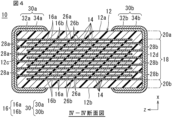
- 4 is a cross-sectional view taken along line IV-IV in FIG. 2.
- 1 is a front view of a multilayer ceramic electronic component according to an embodiment of the present invention.
- FIG. 2 is a bottom view of the multilayer ceramic electronic component according to the embodiment of the present invention.
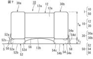
- 1 is a diagram showing a mounting state of a multilayer ceramic electronic component according to an embodiment of the present invention
- FIG. 4 is a bottom view of a multilayer ceramic electronic component according to another embodiment of the present invention.
- FIG. 1 is an external perspective view of a multilayer ceramic electronic component according to an embodiment of the present invention.
- Fig. 2 is an external perspective view of a multilayer ceramic capacitor according to an embodiment of the present invention.
- Fig. 3 is a cross-sectional view taken along line III-III in Fig. 2.
- Fig. 4 is a cross-sectional view taken along line IV-IV in Fig. 2.
- Fig. 5 is a front view of a multilayer ceramic electronic component according to an embodiment of the present invention.
- Fig. 6 is a bottom view of a multilayer ceramic electronic component according to an embodiment of the present invention.
- Fig. 7 is a diagram showing a mounted state of a multilayer ceramic electronic component according to an embodiment of the present invention.
- Fig. 8 is a bottom view of a multilayer ceramic electronic component according to another embodiment of the present invention.
- the multilayer ceramic electronic component 1 of the present invention comprises a multilayer ceramic capacitor 10 having a laminate 12 and two external electrodes 30a, 30b, a first spacer 52 connected to one of the external electrodes 30a, a second spacer 54 connected to the other external electrode 30b, and a third spacer 56 disposed between the first spacer 52 and the second spacer 54.
- the laminate 12 has a hexahedral shape. It is preferable that the corners and ridges of the laminate 12 are rounded. The corners are the parts where three adjacent faces of the laminate 12 intersect, and the ridges are the parts where two adjacent faces of the laminate 12 intersect. Furthermore, unevenness may be formed on some or all of the first face 12a and the second face 12b, the third face 12c and the fourth face 12d, and the fifth face 12e and the sixth face 12f.
- the laminate 12 has an inner layer portion 18 in which multiple internal electrodes 16 face each other.
- the first internal electrode 16a faces the second internal electrode 16b.
- the laminate 12 has a first outer layer 20a located on the first surface 12a side and formed of a plurality of dielectric layers 14 located between the first surface 12a and the outermost surface of the inner layer 18 on the first surface 12a side and an extension of that outermost surface.
- the laminate 12 has a second outer layer 20b located on the second surface 12b side and formed of a plurality of dielectric layers 14 located between the second surface 12b and the outermost surface of the inner layer 18 on the second surface 12b side and an extension of that outermost surface.
- the ceramic material constituting the dielectric layer 14 may be, for example, a dielectric ceramic composed of a main component such as BaTiO3 , CaTiO3 , SrTiO3 , or CaZrO3 .
- a material containing a subcomponent such as a Mn compound, an Fe compound, a Cr compound, a Co compound, or a Ni compound added to the main component may also be used.
- the thickness of the dielectric layer 14 is preferably 0.5 ⁇ m or more and 10 ⁇ m or less. Furthermore, the number of dielectric layers 14, including the first outer layer 20a and the second outer layer 20b, is preferably 10 or more and 700 or less.
- the internal electrode 16 includes a plurality of first internal electrodes 16a and a plurality of second internal electrodes 16b.
- the first internal electrode 16a is disposed on the multiple dielectric layers 14 and is exposed on the third surface 12c.
- the second internal electrode 16b is disposed on the multiple dielectric layers 14 and is exposed on the fourth surface 12d.
- the second internal electrode 16b includes a second opposing electrode portion 26b that faces the first internal electrode 16a, and a second extraction electrode portion 28b that is extracted from the second opposing electrode portion 26b to the fourth surface 12d of the laminate 12.
- the second extraction electrode portion 28b of the second internal electrode 16b has an end portion that is extracted to the surface of the fourth surface 12d of the laminate 12, forming an exposed portion.
- the shape of the first lead electrode portion 28a of the first internal electrode 16a and the second lead electrode portion 28b of the second internal electrode 16b is not particularly limited, but is preferably rectangular. However, the corners may be rounded or angled (tapered).
- capacitance is formed by opposing electrode portions 26 of the internal electrodes 16 facing each other via the dielectric layer 14, and the characteristics of a capacitor are expressed.
- the first internal electrode 16a and the second internal electrode 16b can be made of an appropriate conductive material, such as a metal such as Ni, Cu, Ag, Pd, or Au, or an alloy containing at least one of these metals, such as an Ag-Pd alloy.
- an appropriate conductive material such as a metal such as Ni, Cu, Ag, Pd, or Au, or an alloy containing at least one of these metals, such as an Ag-Pd alloy.
- Sn in the first internal electrode 16a and the second internal electrode 16b, it is possible to reduce electric field concentration at the interface between the internal electrode 16 and the dielectric layer 14, leading to improved high temperature load reliability. In this case, even if Sn is included in only one of the internal electrodes 16, either the first internal electrode 16a or the second internal electrode 16b, it can be sufficiently effective.
- each of the first internal electrode 16a and the second internal electrode 16b is preferably, for example, 0.2 ⁇ m or more and 2.0 ⁇ m or less.
- the number of internal electrodes 16 is preferably 10 or more and 700 or less.
- the external electrode 30 includes a first external electrode 30a and a second external electrode 30b.
- the first external electrode 30a is connected to the first internal electrode 16a and is disposed on the third surface 12c. It may also be disposed on part of the first surface 12a and part of the second surface 12b, part of the fifth surface 12e, and part of the sixth surface 12f. In this embodiment, it is formed extending from the third surface 12c to part of the first surface 12a and part of the second surface 12b, part of the fifth surface 12e, and part of the sixth surface 12f.
- the second external electrode 30b is connected to the second internal electrode 16b and is disposed on the fourth surface 12d. It may also be disposed on part of the first surface 12a and part of the second surface 12b, part of the fifth surface 12e, and part of the sixth surface 12f. In this embodiment, it is formed extending from the fourth surface 12d to part of the first surface 12a and part of the second surface 12b, part of the fifth surface 12e, and part of the sixth surface 12f.
- the first external electrode 30a and the second external electrode 30b have an underlying electrode layer 32 disposed on the surface of the laminate 12 and a plating layer 34 disposed to cover the underlying electrode layer 32.
- the base electrode layer 32 is disposed on the third surface 12c and the fourth surface 12d. Also, on the first external electrode 30a side and the second external electrode 30b side, the base electrode layer 32 may be disposed on a part of the first surface 12a and a part of the second surface 12b, a part of the fifth surface 12e, and a part of the sixth surface 12f. In this embodiment, the base electrode layer 32 is formed so as to extend from the third surface 12c and the fourth surface 12d to a part of the first surface 12a and a part of the second surface 12b, a part of the fifth surface 12e, and a part of the sixth surface 12f on the first external electrode 30a side and the second external electrode 30b side, respectively.
- the base electrode layer 32 has a first base electrode layer 32a and a second base electrode layer 32b.
- the base electrode layer 32 includes at least one selected from a baked layer, a conductive resin layer, a thin film layer, etc.
- the baking layer includes a glass component and a metal.
- the glass component of the baking layer includes at least one selected from, for example, B, Si, Ba, Mg, Al, and Li.
- the metal of the baking layer includes at least one selected from, for example, Cu, Ni, Ag, Pd, an Ag-Pd alloy, Au, and the like.
- the baked layer may be multiple layers.
- the baked layer is formed by applying a conductive paste containing glass and metal to the laminate 12 and baking it.
- the baked layer may be formed by simultaneously baking a laminated chip having an internal electrode 16 and a dielectric layer 14 and a conductive paste applied to the laminated chip, or may be formed by baking a laminated chip having an internal electrode 16 and a dielectric layer 14 to obtain the laminate 12, and then applying a conductive paste to the laminate 12 and baking it.
- a laminated chip having an internal electrode 16 and a dielectric layer 14 and a conductive paste applied to the laminated chip are simultaneously baked, it is preferable to form the baked layer by baking a material to which a dielectric material is added instead of a glass component.
- the thickness in the length direction z connecting the third surface 12c and the fourth surface 12d at the center of the height direction x connecting the first surface 12a and the second surface 12b of the first baked layer located on the third surface 12c is preferably, for example, 3 ⁇ m or more and 160 ⁇ m or less.
- the thickness in the length direction z connecting the third surface 12c and the fourth surface 12d at the center of the height direction x connecting the first surface 12a and the second surface 12b of the second baked layer located on the fourth surface 12d is preferably, for example, 3 ⁇ m or more and 160 ⁇ m or less.
- the thickness in the height direction x connecting the first surface 12a and the second surface 12b at the center of the length direction z connecting the third surface 12c and the fourth surface 12d of the first baked layer located on a part of the first surface 12a and a part of the second surface 12b is preferably, for example, 3 ⁇ m or more and 40 ⁇ m or less.
- the thickness in the height direction x connecting the first surface 12a and the second surface 12b at the center of the length direction z connecting the third surface 12c and the fourth surface 12d of the second baked layer located on a part of the first surface 12a and a part of the second surface 12b is preferably, for example, 3 ⁇ m or more and 40 ⁇ m or less.
- the conductive resin layer may be disposed so as to cover the baked layer. Also, the conductive resin layer may be disposed directly on the laminate 12 without providing a baked layer. The conductive resin layer may completely cover the underlying electrode layer 32 or may cover only a part of the underlying electrode layer 32 .
- the conductive resin layer may be formed of a plurality of layers.
- the conductive resin layer contains, for example, a thermosetting resin and a metal component.
- thermosetting resins that can be used include various known thermosetting resins such as epoxy resin, phenolic resin, urethane resin, silicone resin, and polyimide resin.
- epoxy resin is one of the most suitable resins due to its excellent heat resistance, moisture resistance, and adhesion.
- the conductive resin layer preferably contains a curing agent in addition to the thermosetting resin.
- a curing agent in addition to the thermosetting resin.
- various known compounds such as phenols, amines, acid anhydrides, imidazoles, active esters, and amide-imides can be used as the curing agent.
- the metal contained in the conductive resin layer can be Ag, Cu, Ni, Sn, Bi, or an alloy containing them. Also, a metal powder with an Ag coating on the surface can be used. When using a metal powder with an Ag coating on the surface, it is preferable to use Cu, Ni, Sn, Bi, or an alloy powder of these.
- the reason for using Ag conductive metal powder as the metal contained in the conductive resin layer is that Ag has the lowest resistivity among metals and is therefore suitable as an electrode material, and Ag is a precious metal and therefore does not oxidize and has high weather resistance. Also, it is possible to make the base metal inexpensive while maintaining the above-mentioned characteristics of Ag.
- Cu or Ni that has been subjected to an oxidation prevention treatment can also be used as the metal contained in the conductive resin layer.
- a metal powder with Sn, Ni, or Cu coating on the surface can also be used as the metal contained in the conductive resin layer.
- Ag, Cu, Ni, Sn, Bi, or an alloy powder of these it is preferable to use Ag, Cu, Ni, Sn, Bi, or an alloy powder of these.
- the metal contained in the conductive resin layer can be spherical or flat, but it is preferable to use a mixture of spherical metal powder and flat metal powder.
- the metal contained in the conductive resin layer is mainly responsible for the electrical conductivity of the conductive resin layer. Specifically, when conductive fillers (metal contained in the conductive resin layer) come into contact with each other, an electrical path is formed inside the conductive resin layer.
- the conductive resin layer contains a thermosetting resin, and is therefore more flexible than, for example, an underlying electrode layer made of a plating film or a fired conductive paste. For this reason, even if the multilayer ceramic capacitor is subjected to a physical shock or a shock caused by a thermal cycle, the conductive resin layer functions as a buffer layer and can prevent cracks in the multilayer ceramic capacitor.
- the thickness of the thickest part of the conductive resin layer is preferably, for example, 10 ⁇ m or more and 150 ⁇ m or less.
- the thin film layer is formed by a thin film forming method such as sputtering or vapor deposition, and is a layer of 1 ⁇ m or less in thickness in which metal particles are deposited.
- the plating layer 34 includes a first plating layer 34a and a second plating layer 34b.
- the first plating layer 34a is disposed so as to cover the first base electrode layer 32a.
- the second plating layer 34b is disposed so as to cover the second base electrode layer 32b.
- the plating layer 34 includes at least one selected from the group consisting of Cu, Ni, Sn, Ag, Pd, Ag-Pd alloy, Au, etc.
- the plating layer 34 may be formed of multiple layers. Preferably, it has a two-layer structure of Ni plating and Sn plating.
- the Ni plating layer can prevent the base electrode layer 32 from being eroded by solder when mounting the multilayer ceramic electronic component 1.
- the Sn plating layer improves the wettability of the solder when mounting the multilayer ceramic electronic component 1, making it easier to mount.
- each plating layer 34 is 2 ⁇ m or more and 15 ⁇ m or less.
- the external electrode 30 may be formed using only the plating layer 34 without providing the base electrode layer 32. Below, a structure in which the plating layer 34 is provided without providing the base electrode layer 32 will be described.
- the plating layer 34 includes a lower layer plating electrode formed on the surface of the laminate 12 and an upper layer plating electrode formed on the surface of the lower layer plating electrode.
- the first spacer 52 is disposed between the first external electrode 30a and the mounting surface S, and is connected to the first external electrode 30a.
- the second spacer 54 is disposed between the second external electrode 30b and the mounting surface S, and is connected to the second external electrode 30b.
- the shape may be formed like a cloud shape in which a plurality of convex portions and/or concave portions are formed when viewed from the bottom surface (mounting surface side).
- the first spacer 52 and the second spacer 54 will be described as having a hexahedral shape.
- the edge portion of the first spacer 52 on the center side of the multilayer ceramic capacitor 10 may be located closer to the center than the end of the first external electrode 30a on the center side of the multilayer ceramic capacitor 10.
- the edge portion of the second spacer 54 on the center side of the multilayer ceramic capacitor 10 may be located closer to the center than the end of the second external electrode 30b on the center side of the multilayer ceramic capacitor 10.
- the distance between the inner layer 18, which is the capacitance forming portion of the multilayer ceramic capacitor 10, and the mounting surface S can be increased, thereby suppressing "ringing".
- the dimension T S in the height direction x of the first spacer 52 and the second spacer 54 is preferably, for example, 50 ⁇ m or more and 250 ⁇ m or less.
- the dimension T S in the height direction x of the first spacer 52 and the second spacer 54 is preferably about 160 ⁇ m.
- the first spacer 52 and the second spacer 54 may have unevenness in part. When the first spacer 52 and the second spacer 54 have unevenness in part due to their shapes, it is preferable that the minimum thickness of the dimension T S in the height direction x of the first spacer 52 and the second spacer 54 is about 160 ⁇ m.
- the first spacer 52 and the second spacer 54 contain metal powder.
- the metal powder contains, for example, Cu, Ni, or an alloy of Cu and a metal component (for example, Ni), and Sn.
- Ag or a resin component (for example, rosin) may be contained, and Cu and Ni may be coated with Ag. This allows the laminated ceramic electronic component 1 to be mounted on a substrate while maintaining a desired shape even during soldering because it has a melting point that does not melt even when soldering is performed and does not deform due to heat.
- it is not limited to this, and may contain a different type of metal component.
- first spacer 52 and the second spacer 54 contain Cu, Ni, or an alloy of Cu and a metal component (for example, Ni), and Sn, metal bonding between the first spacer 52 and the second spacer 54 and the external electrodes 30a, 30b of the laminated ceramic capacitor 10 is facilitated.
- the first spacer 52 and the second spacer 54 may contain phenolic resin as a resin component.
- the phenolic resin coats the metal powder particles and is scattered so as to fill the gaps between the particles. Since the phenolic resin has good heat resistance, the amount of vaporization can be reduced during the heat treatment process when forming the spacer. Therefore, the voids within the spacer can be reduced.
- the spacer may contain epoxy resin or rosin in addition to the phenolic resin.
- the first spacer 52 and the second spacer 54 may also be configured to contain metal powder in resin. If the resin component is contained in a larger amount than the metal powder, the vibration of the multilayer ceramic capacitor 10 can be buffered by the resin component, and the vibration transmitted to the substrate can be reduced. In this case, the surfaces of the first spacer 52 and the second spacer 54 may be plated.
- the components of the first spacer 52 and the second spacer 54 can be detected, for example, as follows.
- the multilayer ceramic electronic component 1 is cross-sectionally polished perpendicular to the mounting surface S to 1 ⁇ 6W of the width direction y to expose a cross section (LT surface) in the height direction x and length direction z.
- the components of the first spacer 52 and the second spacer 54 can be detected by qualitative analysis using, for example, EDX of an FE-SEM (SU8230, manufactured by Hitachi High-Technologies Corporation) in the cross section obtained by cross-sectional polishing.
- the cross section obtained by polishing the cross section is magnified at a total magnification of 50 times using a microscope (BX-51, manufactured by Olympus Corporation) and photographed with a digital camera for microscopes (DP22, manufactured by Olympus Corporation), whereby the metal types in the first spacer 52 and the second spacer 54 and, if plating is present on the first spacer 52 and the second spacer 54, the differences in the metal types of the plating can be observed.
- a microscope BX-51, manufactured by Olympus Corporation
- DP22 digital camera for microscopes
- the third spacer 56 is connected to a part of the laminate 12, a part of the first spacer 52, and a part of the second spacer 54. More specifically, the third spacer 56 covers the fourth surface 52d of the first spacer 52 and the third surface 54c of the second spacer 54. It is preferable that the third spacer 56 covers 50% or more of the area of the fourth surface 52d of the first spacer 52, and it is preferable that the third spacer 56 covers 50% or more of the area of the third surface 54c of the second spacer 54. In this case, it is preferable that the third spacer 56 continuously covers the space between the first spacer 52 and the laminate 12, and the space between the second spacer 54 and the laminate 12.
- the third spacer 56 continuously covers the surface of the laminate 12.
- the third spacer 56 may be arranged discontinuously in the longitudinal direction (length direction z) of the multilayer ceramic capacitor 10. This allows the distance between the center portion in the longitudinal direction z, where vibration occurs most, and the multilayer ceramic electronic component 1 to be increased, thereby reducing the possibility of contact between the mounting board and the multilayer ceramic electronic component 1.
- the third spacer 56 may cover the fifth surface 52e and the sixth surface 52f of the first spacer 52, and the fifth surface 54e and the sixth surface 54f of the second spacer 54.
- the third spacer 56 may cover the fifth surface 12e and the sixth surface 12f of the multilayer ceramic capacitor 10 continuously from the fifth surface 52e and the sixth surface 52f of the first spacer 52, and the fifth surface 54e and the sixth surface 54f of the second spacer 54.
- the location where the third spacer 56 covers the multilayer ceramic capacitor 10 is not particularly limited, but it is preferable not to cover the surface (first surface 12a) of the non-mounting surface side of the multilayer ceramic electronic component 1 in order to distinguish the mounting surface side (second surface 12b).
- the central region of the third spacer 56 is a location 1/2L in the length direction z of the multilayer ceramic electronic component 1.
- the end regions of the third spacer 56 are locations where the third spacer 56 contacts the first spacer 52 or the second spacer 54.
- the thickness t1 of the central region of the third spacer 56 is preferably formed thinner than the thicknesses t2 and t3 of the end regions of the third spacer 56.
- the third spacer 56 is arranged so as to draw a curve that is curved toward the mounting surface side.
- the third spacer 56 is shaped so as to be wetted by the first spacer 52 and the second spacer 54. This can reduce the possibility of contact between the third spacer 56 and the mounting surface S when the multilayer ceramic capacitor 10 vibrates.
- the multilayer ceramic electronic component 1 is polished to 1 ⁇ 2W in the width direction y to expose the cross section (LT surface).
- the exposed cross section is measured using a digital microscope (Keyence Corporation, VHX-6000) to measure the distance from the second surface 12b of the multilayer body 12 to the surface of the mounting surface side of the third spacer 56.
- the length w1 in the width direction y of the central region of the third spacer 56 is shorter than the lengths w2 and w3 in the width direction y of the end regions of the third spacer 56.
- the third spacer 56 is preferably disposed between the laminate 12 and the first spacer 52, and between the laminate 12 and the second spacer 54. This fills the gap between the laminate 12 and the first spacer 52, and between the laminate 12 and the second spacer 54 with the third spacer 56, reducing the possibility that the edge portion on the center side of the first spacer 52 (the ridge portion where the first surface 52a and the fourth surface 52d intersect) or the edge portion on the center side of the second spacer 54 (the ridge portion where the first surface 54a and the third surface 54c intersect) will come into contact with and damage the laminate ceramic capacitor 10 when vibration occurs.
- the color of the multilayer ceramic electronic component 1 be different when viewed from the bottom (mounting surface) and when viewed from the top (non-mounting surface).
- the different colors make it easier to select the direction when mounting on a board, and can reduce mounting of the multilayer ceramic electronic component 1 on a surface other than the surface on which it is to be mounted.
- the third spacer 56 includes, for example, carbon, Co, Al, or Cr.
- the third spacer 56 may include an epoxy resin, a hardener, or other organic solvent.
- the hue of the third spacer 56 can be made closer to black. Also, if the third spacer 56 contains a large amount of Co, Al, or Cr, the hue of the third spacer 56 can be made closer to blue. In addition, the hue can be changed by using various other materials.
- the content of the various materials for changing the hue is preferably 0.1 wt% or more and 5.0 wt% or less based on the solid content of the third spacer 56, i.e., the amount of solid content excluding solvent (epoxy resin, phenolic resin), additives (coupling agent, catalyst), and inorganic material (silica, alumina) as a standard. If the weight ratio is small, the change in hue may not be sufficient, and the image may not be correctly recognized during image processing. If the weight ratio is too large, the third spacer 56 may cause electrical conduction between the first external electrode 30a and the second external electrode 30b, or between the first spacer 52 and the second spacer 54.
- hues are different in more than half of the area of the area between the first spacer 52 and the second spacer 54 on the mounting surface side.
- the first surface 12a, which is the non-mounting surface side, and the second surface 12b, which is the mounting surface side, of the multilayer ceramic electronic component 1 are measured (RGB measurement) using a digital microscope (Keyence Corporation, VHX-6000).
- the measurement conditions are brightness auto "100", gain auto "100", and ring removal "medium” for reflection removal.
- the conductive paste for the dielectric sheet and the internal electrodes contains a binder and a solvent.
- Publicly known binders and solvents can be used.
- the laminated sheet is pressed in the stacking direction using a means such as a hydrostatic press to create a laminated block.
- a conductive paste that will become the base electrode layer 32 is applied to the third surface 12c and the fourth surface 12d of the laminate 12 to form the base electrode layer 32.
- a baked layer is formed as the base electrode layer 32.
- a conductive paste containing a glass component and a metal is applied by a method such as dipping, and then a baking process is performed to form the base electrode layer 32.
- the temperature of the baking process at this time is preferably 700°C or higher and 900°C or lower.
- the conductive resin layer can be formed by the following method.
- the conductive resin layer may be formed on the surface of the baked layer, or the conductive resin layer may be formed directly on the laminate without forming a baked layer.
- the third surface 12c and the fourth surface 12d of the laminate 12 are plated to form an underlayer plating electrode on the exposed portion of the internal electrode 16.
- Either electrolytic plating or electroless plating may be used for the plating process, but electroless plating has the disadvantage that it requires pretreatment with a catalyst or the like to improve the plating deposition rate, which complicates the process. Therefore, it is usually preferable to use electrolytic plating.
- As a plating method it is preferable to use barrel plating.
- an upper layer plating electrode may be formed on the surface of the lower layer plating electrode in a similar manner.
- a plating layer 34 is formed on the surface of the base electrode layer 32, the surface of the conductive resin layer or the surface of the lower layer plating electrode, and the surface of the upper layer plating electrode.
- a Ni plating layer and a Sn plating layer are formed on the baked layer.
- the Ni plating layer and the Sn plating layer are formed in sequence, for example, by barrel plating.
- the multilayer ceramic capacitor 10 is manufactured.
- first external electrode 30a and the first spacer manufacturing paste, and the second external electrode 30b and the second spacer manufacturing paste are aligned, and the first spacer manufacturing paste and the second spacer manufacturing paste are attached to the multilayer ceramic capacitor 10. Thereafter, a heat treatment is performed to form the first spacer 52 and the second spacer 54.
- the first spacer 52 and the second spacer 54 can also be disposed in the multilayer ceramic capacitor 10 by the following method.
- the multilayer ceramic capacitor 10 is placed on a holding substrate (e.g., an alumina plate) using an adhesive.
- Each spacer manufacturing paste is placed on the external electrodes 30 of the multilayer ceramic capacitor 10 placed on the holding substrate by a screen printing method, a dispensing method, or the like.
- the first external electrode 30a and the first spacer manufacturing paste, and the second external electrode 30b and the second spacer manufacturing paste are aligned, and the first spacer manufacturing paste and the second spacer manufacturing paste are attached to the multilayer ceramic capacitor 10.
- the first spacer 52 and the second spacer 54 can be formed in the desired shape and placement by changing the amount of paste or modifying the mask design. After that, the first spacer 52 and the second spacer 54 are formed by performing a heat treatment.
- the surface of the multilayer ceramic capacitor 10 on which the first spacer 52 and the second spacer 54 are arranged is cleaned with a solvent. After cleaning is completed, the multilayer ceramic capacitor 10 on which the first spacer 52 and the second spacer 54 are arranged is aligned so that the first spacer 52 and the second spacer 54 face upwards.
- the paste for manufacturing the third spacer 56 is composed of an insulating paste.
- the hue of the third spacer 56 can be changed by adding various materials as additives.
- a third spacer 56 is formed between the first spacer 52 and the second spacer 54 using a dispenser or squeegee printing on the multilayer ceramic capacitor 10 on which the first spacer 52 and the second spacer 54 are arranged.
- the amount of wetting of the first spacer 52 and the second spacer 54 can be changed by changing the amount of paste for manufacturing the third spacer.
- the third spacer 56 When inserting a third spacer 56 between the laminate 12 and the first spacer 52, or between the laminate 12 and the second spacer 54, the third spacer 56 can be inserted by applying a vacuum after placing the paste for manufacturing the third spacer.
- the amount of insertion can be controlled by changing the time and pressure of the vacuum.
- a multilayer ceramic capacitor including a laminate and two external electrodes; a first spacer connected to one of the external electrodes; a second spacer connected to the other external electrode; a third spacer disposed between the first spacer and the second spacer,
- the laminate comprises: A first surface is a surface on a non-mounting side, The first surface and the third spacer have different hues.
- ⁇ 4> The multilayer ceramic electronic component according to any one of ⁇ 1> to ⁇ 3>, wherein the third spacer is disposed between the laminate and the first spacer, or between the laminate and the second spacer.
- ⁇ 5> The multilayer ceramic electronic component according to any one of ⁇ 1> to ⁇ 4>, wherein a lamination direction of the laminate is perpendicular to a mounting surface.
- ⁇ 6> In the longitudinal direction of the multilayer ceramic capacitor, The multilayer ceramic electronic component according to any one of ⁇ 1> to ⁇ 5>, wherein a length in the width direction of the central region of the third spacer is shorter than a length in the width direction of an end region of the third spacer.
- ⁇ 7> The multilayer ceramic electronic component according to any one of ⁇ 1> to ⁇ 6>, wherein the third spacer is disposed between the laminate and the first spacer, and between the laminate and the second spacer.
- a multilayer ceramic capacitor including a laminate and two external electrodes; a first spacer connected to one of the external electrodes; a second spacer connected to the other external electrode; Equipped with The laminate comprises: a second surface which is a mounting surface side; and a first surface which is a non-mounting side surface and faces the second surface; a mounting surface and a non-mounting surface of the laminate have different hues in a direction connecting the first surface and the second surface.
- ⁇ 9> The multilayer ceramic electronic component according to any one of ⁇ 1> to ⁇ 8>, wherein the content of the material for changing the hue is 0.1 wt % or more and 5.0 wt % or less based on the amount of solids excluding the solvent, additives, and inorganic materials.
- Multilayer ceramic electronic component 10 Multilayer ceramic capacitor 12 Laminate 12a First surface 12b Second surface 12c Third surface 12d Fourth surface 12e Fifth surface 12f Sixth surface 14 Dielectric layer 16 Internal electrode 16a First internal electrode 16b Second internal electrode 18 Internal layer portion 20a First outer layer portion 20b Second outer layer portion 26 Counter electrode portion 26a First counter electrode portion 26b Second counter electrode portion 28 Lead electrode portion 28a First lead electrode portion 28b Second lead electrode portion 30 External electrode 30a First external electrode 30b Second external electrode 32 Base electrode layer 32a First base electrode layer 32b Second base electrode layer 34 Plating layer 34a First plating layer 34b second plating layer 50 spacer 52 first spacer 52a first surface of first spacer 52b second surface of first spacer 52c third surface of first spacer 52d fourth surface of first spacer 52e fifth surface of first spacer 52f sixth surface of first spacer 54 second spacer 54a first surface of second spacer 54b second surface of second spacer 54c third surface of second spacer 54d fourth surface of second spacer 54e fifth surface of second
Landscapes
- Engineering & Computer Science (AREA)
- Power Engineering (AREA)
- Microelectronics & Electronic Packaging (AREA)
- Manufacturing & Machinery (AREA)
- Fixed Capacitors And Capacitor Manufacturing Machines (AREA)
- Ceramic Capacitors (AREA)
Priority Applications (3)
| Application Number | Priority Date | Filing Date | Title |
|---|---|---|---|
| CN202480055539.9A CN121794775A (zh) | 2023-08-29 | 2024-04-03 | 层叠陶瓷电子部件 |
| KR1020267006352A KR20260048297A (ko) | 2023-08-29 | 2024-04-03 | 적층 세라믹 전자부품 |
| JP2025542694A JPWO2025046969A1 (https=) | 2023-08-29 | 2024-04-03 |
Applications Claiming Priority (2)
| Application Number | Priority Date | Filing Date | Title |
|---|---|---|---|
| JP2023139087 | 2023-08-29 | ||
| JP2023-139087 | 2023-08-29 |
Publications (1)
| Publication Number | Publication Date |
|---|---|
| WO2025046969A1 true WO2025046969A1 (ja) | 2025-03-06 |
Family
ID=94818654
Family Applications (1)
| Application Number | Title | Priority Date | Filing Date |
|---|---|---|---|
| PCT/JP2024/013805 Pending WO2025046969A1 (ja) | 2023-08-29 | 2024-04-03 | 積層セラミック電子部品 |
Country Status (4)
| Country | Link |
|---|---|
| JP (1) | JPWO2025046969A1 (https=) |
| KR (1) | KR20260048297A (https=) |
| CN (1) | CN121794775A (https=) |
| WO (1) | WO2025046969A1 (https=) |
Citations (2)
| Publication number | Priority date | Publication date | Assignee | Title |
|---|---|---|---|---|
| JP2019067953A (ja) * | 2017-10-02 | 2019-04-25 | 太陽誘電株式会社 | 電子部品、電子装置、電子部品の製造方法、及び電子部品の識別方法 |
| JP2022099069A (ja) * | 2020-12-22 | 2022-07-04 | 株式会社村田製作所 | 積層セラミックコンデンサ及び積層セラミックコンデンサの製造方法 |
-
2024
- 2024-04-03 CN CN202480055539.9A patent/CN121794775A/zh active Pending
- 2024-04-03 KR KR1020267006352A patent/KR20260048297A/ko active Pending
- 2024-04-03 WO PCT/JP2024/013805 patent/WO2025046969A1/ja active Pending
- 2024-04-03 JP JP2025542694A patent/JPWO2025046969A1/ja active Pending
Patent Citations (2)
| Publication number | Priority date | Publication date | Assignee | Title |
|---|---|---|---|---|
| JP2019067953A (ja) * | 2017-10-02 | 2019-04-25 | 太陽誘電株式会社 | 電子部品、電子装置、電子部品の製造方法、及び電子部品の識別方法 |
| JP2022099069A (ja) * | 2020-12-22 | 2022-07-04 | 株式会社村田製作所 | 積層セラミックコンデンサ及び積層セラミックコンデンサの製造方法 |
Also Published As
| Publication number | Publication date |
|---|---|
| JPWO2025046969A1 (https=) | 2025-03-06 |
| KR20260048297A (ko) | 2026-04-09 |
| CN121794775A (zh) | 2026-04-03 |
Similar Documents
| Publication | Publication Date | Title |
|---|---|---|
| JP6806035B2 (ja) | 積層セラミックコンデンサ | |
| US10475584B2 (en) | Electronic component mount structure, electronic component, and method for manufacturing electronic component | |
| US11062848B2 (en) | Multilayer ceramic electronic component | |
| JP7559849B2 (ja) | 積層セラミック電子部品 | |
| JP2015053495A (ja) | セラミック電子部品およびその製造方法 | |
| JP2017220523A (ja) | 積層セラミック電子部品 | |
| US20260024699A1 (en) | Multilayer ceramic electronic component | |
| JP2022077451A (ja) | 積層セラミックコンデンサ | |
| WO2025046969A1 (ja) | 積層セラミック電子部品 | |
| WO2026009776A1 (ja) | 積層セラミック電子部品 | |
| WO2025234429A1 (ja) | 積層セラミック電子部品 | |
| WO2026009777A1 (ja) | 積層セラミック電子部品 | |
| WO2025225548A1 (ja) | 積層セラミック電子部品 | |
| WO2025187811A1 (ja) | 積層セラミック電子部品 | |
| US20260011502A1 (en) | Laminated ceramic electronic component | |
| US20260011504A1 (en) | Multilayer ceramic electronic component | |
| WO2025192599A1 (ja) | 積層セラミック電子部品 | |
| JP2022163423A (ja) | 積層セラミックコンデンサ | |
| US20260018337A1 (en) | Multilayer ceramic electronic component | |
| JP7751261B2 (ja) | 積層セラミックコンデンサ | |
| US20250329496A1 (en) | Multilayer ceramic capacitor | |
| US20260018340A1 (en) | Multilayer ceramic electronic component | |
| WO2026063477A1 (ja) | 積層セラミック電子部品 | |
| WO2026063476A1 (ja) | 積層セラミック電子部品 | |
| JP2019179820A (ja) | 積層セラミックコンデンサ |
Legal Events
| Date | Code | Title | Description |
|---|---|---|---|
| 121 | Ep: the epo has been informed by wipo that ep was designated in this application |
Ref document number: 24859018 Country of ref document: EP Kind code of ref document: A1 |
|
| ENP | Entry into the national phase |
Ref document number: 2025542694 Country of ref document: JP Kind code of ref document: A |
|
| WWE | Wipo information: entry into national phase |
Ref document number: 2025542694 Country of ref document: JP |
|
| ENP | Entry into the national phase |
Ref document number: 1020267006352 Country of ref document: KR Free format text: ST27 STATUS EVENT CODE: A-0-1-A10-A15-NAP-PA0105 (AS PROVIDED BY THE NATIONAL OFFICE) |