WO2025041202A1 - Multi-zone ceramic heater - Google Patents
Multi-zone ceramic heater Download PDFInfo
- Publication number
- WO2025041202A1 WO2025041202A1 PCT/JP2023/029889 JP2023029889W WO2025041202A1 WO 2025041202 A1 WO2025041202 A1 WO 2025041202A1 JP 2023029889 W JP2023029889 W JP 2023029889W WO 2025041202 A1 WO2025041202 A1 WO 2025041202A1
- Authority
- WO
- WIPO (PCT)
- Prior art keywords
- zone
- heater circuit
- ceramic
- ceramic plate
- outer zone
- Prior art date
- Legal status (The legal status is an assumption and is not a legal conclusion. Google has not performed a legal analysis and makes no representation as to the accuracy of the status listed.)
- Pending
Links
Images


Classifications
-
- H—ELECTRICITY
- H05—ELECTRIC TECHNIQUES NOT OTHERWISE PROVIDED FOR
- H05B—ELECTRIC HEATING; ELECTRIC LIGHT SOURCES NOT OTHERWISE PROVIDED FOR; CIRCUIT ARRANGEMENTS FOR ELECTRIC LIGHT SOURCES, IN GENERAL
- H05B3/00—Ohmic-resistance heating
- H05B3/20—Heating elements having extended surface area substantially in a two-dimensional [2D] plane, e.g. plate-heater
- H05B3/22—Heating elements having extended surface area substantially in a two-dimensional [2D] plane, e.g. plate-heater non-flexible
- H05B3/28—Heating elements having extended surface area substantially in a two-dimensional [2D] plane, e.g. plate-heater non-flexible heating conductor embedded in insulating material
- H05B3/283—Heating elements having extended surface area substantially in a two-dimensional [2D] plane, e.g. plate-heater non-flexible heating conductor embedded in insulating material the insulating material being an inorganic material, e.g. ceramic
-
- H—ELECTRICITY
- H05—ELECTRIC TECHNIQUES NOT OTHERWISE PROVIDED FOR
- H05B—ELECTRIC HEATING; ELECTRIC LIGHT SOURCES NOT OTHERWISE PROVIDED FOR; CIRCUIT ARRANGEMENTS FOR ELECTRIC LIGHT SOURCES, IN GENERAL
- H05B2203/00—Aspects relating to Ohmic resistive heating covered by group H05B3/00
- H05B2203/002—Heaters using a particular layout for the resistive material or resistive elements
- H05B2203/005—Heaters using a particular layout for the resistive material or resistive elements using multiple resistive elements or resistive zones isolated from each other
-
- H—ELECTRICITY
- H05—ELECTRIC TECHNIQUES NOT OTHERWISE PROVIDED FOR
- H05B—ELECTRIC HEATING; ELECTRIC LIGHT SOURCES NOT OTHERWISE PROVIDED FOR; CIRCUIT ARRANGEMENTS FOR ELECTRIC LIGHT SOURCES, IN GENERAL
- H05B2203/00—Aspects relating to Ohmic resistive heating covered by group H05B3/00
- H05B2203/016—Heaters using particular connecting means
Definitions
- This disclosure relates to a multi-zone ceramic heater.
- Ceramic heaters are used as support stages to uniformly control the temperature of wafers.
- a widely used ceramic heater of this type is one that has a ceramic plate on which the wafer is placed and a cylindrical ceramic shaft attached to the ceramic plate.
- Multi-zone ceramic heaters that have multiple heating zones are also known as ceramic heaters.
- Patent Document 1 JP 2020-191315 A discloses a heating device that includes a first heater electrode arranged in a substantially circular first region and a second heater electrode arranged in a substantially annular second region surrounding the first heater electrode, both in a plate-shaped member.
- This heating device includes a common driver electrode that is electrically connected to all of the heater electrodes and is also electrically connected to a common power supply terminal, and this common driver electrode has a thick portion that is thicker than the thickness of other portions of the common driver electrode. In other words, it discloses that the thickness of the common driver electrode varies partially within its surface.
- Patent document 2 JP 2015-191837 A discloses a laminated heating element having an inner heater and an outer heater around the inner heater.
- This laminated heating element has a ceramic body, a heater built into the body, a terminal attached to one end of the body in the thickness direction, and a power supply path that supplies power from the terminal to the heater.
- the power supply path is composed of a combination of multiple conductive layers and multiple through vias provided in the body.
- conductive layer X which is located closer to the terminal than the heater, has a connection part P with through via ⁇ and a connection part Q with through via ⁇ , and includes at least a part of the path connecting connection part P and connection part Q.
- This conductive layer X has an area AX with a thickness greater than its surroundings.
- Ceramic heaters are required to have small temperature differences (i.e., thermal uniformity) within the surface on which the wafer is placed. In particular, with the recent trend toward finer processing and higher integration, ceramic heaters are required to have even greater thermal uniformity. From this perspective, it is desirable to minimize the temperature difference between the locations where the resistive heating element is present and those where it is not. To achieve this, it is preferable to place the resistive heating element all over the entire area of the ceramic heater, and a promising candidate for this is a printed resistive heating element.
- the inventors have now discovered that in a multi-zone ceramic heater equipped with an inner zone heater circuit, an outer zone heater circuit, and a jumper, by setting the thickness of the jumper within the range of 1.2 to 3.0 times the thickness of the outer zone heater circuit, it is possible to achieve good thermal uniformity while suppressing breakage during manufacturing, etc.
- the object of the present invention is therefore to provide a multi-zone ceramic heater that can achieve good thermal uniformity while minimizing damage during manufacturing, etc.
- a ceramic plate having a circular shape and a first surface on which a wafer is placed and a second surface opposite to the first surface, the ceramic plate including, when viewed from above, an inner zone defined as a circular region within a predetermined distance from a center of the ceramic plate, and an outer zone defined as an annular region outside the inner zone; an inner zone heater circuit embedded in the inner zone of the ceramic plate parallel to the first surface; an outer zone heater circuit embedded in the outer zone of the ceramic plate parallel to the first surface at a depth different from that of the inner zone heater circuit; a pair of first power supply terminals provided at a central portion of the inner zone of the ceramic plate for supplying power to the inner zone heater circuit; a pair of second power supply terminals provided at a central portion of the inner zone of the ceramic plate for supplying power to the outer zone heater circuit; a pair of jumpers separated from each other and embedded in the inner zone of the ceramic plate at the same depth as the outer zone heater circuit and parallel to the first
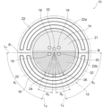
- the outer zone is composed of a plurality of outer subzones partitioned into a circular arc shape, and a linear boundary region, which is not crossed by the outer zone heater circuit, exists between the outer subzones adjacent in the circumferential direction in the radial direction of the ceramic plate so as not to completely divide the outer zone;
- the multi-zone ceramic heater of claim 1 wherein the outer zone heater circuit starts in one or two directions from the first connection portion, and in each starting direction, in a unicursal manner, passes through substantially the entire area of each of the plurality of outer subzones, alternately proceeding in a circumferential direction and turning back just before the boundary region, in a serpentine manner, to reach the second connection portion.
- Aspect 8 Aspect 8.
- each of the inner zone heater circuit, the outer zone heater circuit, and the jumper is in the form of a printed pattern.
- a multi-zone ceramic heater according to any one of the preceding aspects wherein the outer zone heater circuits have a constant thickness in an in-plane direction and the jumpers have a constant thickness in an in-plane direction.
- Aspect 11 Aspect 11.
- the ceramic plate comprises aluminum nitride or aluminum oxide.
- the resistive heating element comprises at least one selected from the group consisting of tungsten, molybdenum, a tungsten-molybdenum alloy, tungsten carbide, a tungsten carbide-titanium nitride composite, and a tungsten carbide-aluminum oxide composite.
- the jumper has a thickness that is 1.8 to 3.0 times the thickness of the outer zone heater circuit.
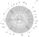
- FIG. 1 is a schematic top view showing an example of a multi-zone ceramic heater according to the present invention.
- FIG. 2 is a schematic cross-sectional view showing the multi-zone ceramic heater shown in FIG. 1.
- FIG. 1 is a schematic top view of a simplified multi-zone ceramic heater for conceptualizing a series circuit.
- FIG. 1 is a schematic top view of a simplified multi-zone ceramic heater for conceptualizing a parallel circuit.
- FIG. 2 is a schematic top view showing another example of a multi-zone ceramic heater, corresponding to Example 1.
- FIG. 11 is a schematic top view showing another example of a multi-zone ceramic heater, corresponding to Examples 2 and 10.
- FIG. 11 is a schematic top view showing another example of a multi-zone ceramic heater, corresponding to Examples 3 and 5.
- FIG. 1 is a schematic top view showing an example of a multi-zone ceramic heater according to the present invention.
- FIG. 2 is a schematic cross-sectional view showing the multi-zone ceramic heater shown in FIG. 1.
- FIG. 11 is a schematic top view showing another example of a multi-zone ceramic heater, corresponding to Examples 4, 7 and 8.
- FIG. 11 is a schematic top view showing another example of a multi-zone ceramic heater, corresponding to Example 6.
- FIG. 11 is a schematic top view showing an example of a multi-zone ceramic heater, corresponding to Example 9 (Comparative Example).
- FIG. 11 is a schematic cross-sectional view showing the multi-zone ceramic heater shown in FIG. 10, corresponding to Example 9 (Comparative Example).
- the multi-zone ceramic heater according to the present invention is a ceramic platform for supporting a wafer in a semiconductor manufacturing device.
- the ceramic heater according to the present invention can be a ceramic heater for a semiconductor film deposition device.
- film deposition devices include CVD (chemical vapor deposition) devices (e.g., thermal CVD devices, plasma CVD devices, photo CVD devices, and MOCVD devices) and PVD (physical vapor deposition) devices.
- the multi-zone ceramic heater 10 shown in Figs. 1 and 2 comprises a ceramic plate 12, an inner zone heater circuit 14, an outer zone heater circuit 16, a pair of first power supply terminals 18, a pair of second power supply terminals 20, and a pair of jumpers 22.
- the ceramic plate 12 is disk-shaped and has a first surface 12a on which a wafer W is placed and a second surface 12b opposite the first surface 12a.
- the ceramic plate 12 includes an inner zone Z1 defined as a circular region within a predetermined distance from the center of the ceramic plate 12, and an outer zone Z2 defined as an annular region outside the inner zone Z1.
- An inner zone heater circuit 14 is embedded in the inner zone Z1 of the ceramic plate 12 parallel to the first surface 12a, while an outer zone heater circuit 16 is embedded in the outer zone Z2 of the ceramic plate 12 parallel to the first surface 12a at a depth different from that of the inner zone heater circuit 14.
- a pair of first power supply terminals 18 are terminals for supplying power to the inner zone heater circuit 14 and are provided in the center of the inner zone Z1 of the ceramic plate 12.
- a pair of second power supply terminals 20 are terminals for supplying power to the outer zone heater circuit 16 and are provided in the center of the inner zone Z1 of the ceramic plate 12.
- a pair of jumpers 22 are separated from each other and embedded in the inner zone Z1 of the ceramic plate 12 parallel to the first surface 12a at the same depth as the outer zone heater circuit 16.
- One of the pair of jumpers 22 electrically connects one of the second power supply terminals 20 to the outer zone heater circuit 16 at a first connection 24, while the other of the pair of jumpers 22 electrically connects the other of the second power supply terminals 20 to the outer zone heater circuit 16 at a second connection 26 at a position different from the first connection 24.
- Each of the inner zone heater circuit 14, the outer zone heater circuit 16, and the jumper 22 is a thin element made of a resistance heating element selected from the group consisting of a printed pattern, a foil, a punched metal, and a mesh.
- the thickness of the jumper 22 is 1.2 to 3.0 times the thickness of the outer zone heater circuit 16.
- the outer zone heater circuit 16 and the jumper 22 by setting the thickness of the jumper 22 within the range of 1.2 to 3.0 times the thickness of the outer zone heater circuit 16, it is possible to achieve good thermal uniformity while suppressing damage during manufacturing, etc.
- ceramic heaters are required to have even greater thermal uniformity (for example, a maximum temperature difference within the surface of 1°C or less). For this reason, it is preferable to place resistance heating elements all over the entire area of the ceramic heater, and a printing type resistance heating element is a promising candidate for this purpose.
- a multi-zone ceramic heater in which a ceramic shaft is placed in the center of a ceramic plate in which a thin resistance heating element (for example, a thickness of 100 ⁇ m or less) is embedded, local hot spots and cool spots are likely to occur in the electrical connection path (jumper connection) from the center of the plate to the resistance heating element on the outer periphery of the plate due to heat generation in the electrical connection path itself.
Landscapes
- Engineering & Computer Science (AREA)
- Chemical & Material Sciences (AREA)
- Ceramic Engineering (AREA)
- Inorganic Chemistry (AREA)
- Resistance Heating (AREA)
- Surface Heating Bodies (AREA)
- Furnace Details (AREA)
- Manufacturing & Machinery (AREA)
Abstract
Description
本開示は、マルチゾーンセラミックヒータに関するものである。 This disclosure relates to a multi-zone ceramic heater.
半導体製造プロセス用の成膜装置において、ウェハの温度を均一に制御するための支持ステージとして、セラミックヒータが用いられている。そのようなセラミックヒータとして、ウェハが載置されるためのセラミックプレートと、このセラミックプレートに取り付けられた円筒状のセラミックシャフトとを備えたものが広く用いられている。また、セラミックヒータとして複数の加熱ゾーンを有するマルチゾーンセラミックヒータも知られている。 In film deposition equipment for semiconductor manufacturing processes, ceramic heaters are used as support stages to uniformly control the temperature of wafers. A widely used ceramic heater of this type is one that has a ceramic plate on which the wafer is placed and a cylindrical ceramic shaft attached to the ceramic plate. Multi-zone ceramic heaters that have multiple heating zones are also known as ceramic heaters.
特許文献1(特開2020-191315号公報)には、略円形の第1の領域に配置される第1のヒータ電極と、その周囲の略環状の第2の領域に配置される第2のヒータ電極とを板状部材内に備えた加熱装置が開示されている。この加熱装置は、複数のヒータ電極の全てに対して電気的に接続され、かつ、共通給電端子に電気的に接続された共通ドライバ電極を備えており、この共通ドライバ電極は、共通ドライバ電極における他の部分の厚さよりも厚い肉厚部分を有している。すなわち、共通ドライバ電極の厚さがその面内で部分的に異なることが開示されている。 Patent Document 1 (JP 2020-191315 A) discloses a heating device that includes a first heater electrode arranged in a substantially circular first region and a second heater electrode arranged in a substantially annular second region surrounding the first heater electrode, both in a plate-shaped member. This heating device includes a common driver electrode that is electrically connected to all of the heater electrodes and is also electrically connected to a common power supply terminal, and this common driver electrode has a thick portion that is thicker than the thickness of other portions of the common driver electrode. In other words, it discloses that the thickness of the common driver electrode varies partially within its surface.
特許文献2(特開2015-191837号公報)には、インナーヒータとその外周のアウターヒータとを有する積層発熱体が開示されている。この積層発熱体は、セラミック製の本体部と、本体部に内蔵されたヒータと、本体部の厚み方向の一端に取り付けられた端子と、端子からヒータに給電する給電経路とを備えている。給電経路は、本体部内に設けられた複数の導電層及び複数のスルービアの組合せで構成される。複数の導電層のうち、ヒータよりも端子側に位置する導電層Xは、スルービアαとの接続部Pと、スルービアβとの接続部Qとを有し、かつ、接続部Pと接続部Qとを結ぶ経路の少なくとも一部を含む。この導電層Xは、その周囲より膜厚が大きい領域AXを有する。 Patent document 2 (JP 2015-191837 A) discloses a laminated heating element having an inner heater and an outer heater around the inner heater. This laminated heating element has a ceramic body, a heater built into the body, a terminal attached to one end of the body in the thickness direction, and a power supply path that supplies power from the terminal to the heater. The power supply path is composed of a combination of multiple conductive layers and multiple through vias provided in the body. Of the multiple conductive layers, conductive layer X, which is located closer to the terminal than the heater, has a connection part P with through via α and a connection part Q with through via β, and includes at least a part of the path connecting connection part P and connection part Q. This conductive layer X has an area AX with a thickness greater than its surroundings.
セラミックヒータにはウェハが載置される面内における温度差が小さいこと(すなわち均熱性)が求められている。とりわけ、近年のプロセスの微細化及び高集積化に伴い、セラミックヒータにはより一層の均熱性が求められている。かかる観点から、抵抗発熱体が存在する場所とそうでない場所の温度差を最小化することが望まれる。そのためには、セラミックヒータの全領域に隈なく抵抗発熱体を配置するのが好ましく、そのための有望な候補として印刷方式の抵抗発熱体が挙げられる。しかし、薄い抵抗発熱体が埋設されたセラミックプレートの中央部にセラミックシャフトが配置されたマルチゾーンセラミックヒータでは、プレート中央部からプレート外周部の抵抗発熱体への電気接続経路(ジャンパ接続)において、電気接続経路自体の発熱に起因して局所的なホットスポットやクールスポットを生じやすい。その影響でマルチゾーンセラミックヒータのプレート部全体の均熱性が悪化する問題があった。 Ceramic heaters are required to have small temperature differences (i.e., thermal uniformity) within the surface on which the wafer is placed. In particular, with the recent trend toward finer processing and higher integration, ceramic heaters are required to have even greater thermal uniformity. From this perspective, it is desirable to minimize the temperature difference between the locations where the resistive heating element is present and those where it is not. To achieve this, it is preferable to place the resistive heating element all over the entire area of the ceramic heater, and a promising candidate for this is a printed resistive heating element. However, in a multi-zone ceramic heater in which a ceramic shaft is placed in the center of a ceramic plate in which a thin resistive heating element is embedded, localized hot spots and cool spots are likely to occur in the electrical connection path (jumper connection) from the center of the plate to the resistive heating element on the outer periphery of the plate due to heat generation in the electrical connection path itself. As a result, there was a problem of deterioration in the thermal uniformity of the entire plate part of the multi-zone ceramic heater.
本発明者らは、今般、内側ゾーンヒータ回路、外側ゾーンヒータ回路及びジャンパを備えたマルチゾーンセラミックヒータにおいて、ジャンパの厚さを外側ゾーンヒータ回路の厚さの1.2~3.0倍の範囲内とすることで、製造時等における破損を抑制しながら、良好な均熱性を実現できることを見出した。 The inventors have now discovered that in a multi-zone ceramic heater equipped with an inner zone heater circuit, an outer zone heater circuit, and a jumper, by setting the thickness of the jumper within the range of 1.2 to 3.0 times the thickness of the outer zone heater circuit, it is possible to achieve good thermal uniformity while suppressing breakage during manufacturing, etc.
したがって、本発明の目的は、製造時等における破損を抑制しながら、良好な均熱性を実現可能なマルチゾーンセラミックヒータを提供することにある。 The object of the present invention is therefore to provide a multi-zone ceramic heater that can achieve good thermal uniformity while minimizing damage during manufacturing, etc.
本開示によれば、以下の態様が提供される。
[態様1]
ウェハが載置されるための第一面と、前記第一面と対向する第二面とを有する円板状のセラミックプレートであって、前記セラミックプレートを平面視した場合に、前記セラミックプレートの中心から所定距離以内の円形領域として規定される内側ゾーンと、前記内側ゾーンの外側の円環状領域として規定される外側ゾーンとを含む、セラミックプレートと、
前記セラミックプレートの前記内側ゾーンに、前記第一面と平行に埋設される、内側ゾーンヒータ回路と、
前記セラミックプレートの前記外側ゾーンに、前記内側ゾーンヒータ回路とは異なる深さ位置で前記第一面と平行に埋設される、外側ゾーンヒータ回路と、
前記セラミックプレートの前記内側ゾーンの中央部に設けられ、前記内側ゾーンヒータ回路に給電するための1対の第一給電端子と、
前記セラミックプレートの前記内側ゾーンの中央部に設けられ、前記外側ゾーンヒータ回路に給電するための1対の第二給電端子と、
前記セラミックプレートの前記内側ゾーンに、前記外側ゾーンヒータ回路と同じ深さ位置で前記第一面と平行に埋設される、互いに分離された1対のジャンパであって、前記1対のジャンパの一方が前記第二給電端子の一方と前記外側ゾーンヒータ回路とを第一接続部で電気的に接続し、かつ、前記1対のジャンパの他方が前記第二給電端子の他方と前記外側ゾーンヒータ回路とを前記第一接続部とは異なる位置の第二接続部で電気的に接続する、1対のジャンパと、
を備え、
前記内側ゾーンヒータ回路、前記外側ゾーンヒータ回路及び前記ジャンパの各々が、印刷パターン、箔、パンチングメタル及びメッシュからなる群から選択される、抵抗発熱体で構成された薄型エレメントであり、
前記ジャンパの厚さが、前記外側ゾーンヒータ回路の厚さの1.2~3.0倍である、マルチゾーンセラミックヒータ。
[態様2]
前記外側ゾーンが、円弧状に区画された複数の外側サブゾーンで構成されており、円周方向に隣り合う前記外側サブゾーンの間に、前記外側ゾーンヒータ回路が横切らない線状の境界領域が、前記外側ゾーンを完全に分断しないように前記セラミックプレートの半径方向に存在しており、
前記外側ゾーンヒータ回路は、前記第一接続部から一方向又は二方向に出発して、各出発方向について一筆書きの要領で、前記複数の外側サブゾーンの各々を概ね全域にわたって通過するように、円周方向への進行及び前記境界領域の手前での折り返しを交互に繰り返しながら蛇行して、前記第二接続部に到達するように設けられる、態様1に記載のマルチゾーンセラミックヒータ。
[態様3]
前記セラミックプレートを平面視した場合に、前記第一接続部及び前記第二接続部の各々について、前記接続部に最も近い前記境界領域の円周方向の中心と前記セラミックプレートの中心とを通る直線と、前記接続部の円周方向の中心とセラミックプレートの中心とを通る直線とが成す角度が20°以上となるように、前記境界領域と前記接続部が離間して配置されている、態様2に記載のマルチゾーンセラミックヒータ。
[態様4]
前記第一接続部及び前記第二接続部の各々を前記内側ゾーンの外周円を構成する円弧とみなした場合に、前記円弧の各々の中心角が6.0~10.0°の範囲内である、態様1~3のいずれか一つに記載のマルチゾーンセラミックヒータ。
[態様5]
前記外側ゾーンヒータ回路が、直列回路を成すように、前記第一接続部から一方向に出発して、一筆書きの要領で前記第二接続部に到達するように設けられる、態様1~4のいずれか一つに記載のマルチゾーンセラミックヒータ。
[態様6]
前記外側ゾーンヒータ回路が、並列回路を成すように、前記第一接続部から二方向に出発して、各出発方向について一筆書きの要領で前記第二接続部に到達するように設けられる、態様1~4のいずれか一つに記載のマルチゾーンセラミックヒータ。
[態様7]
前記セラミックプレートを平面視した場合、前記1対のジャンパ及び前記1対の第二給電端子が、前記1対の第二給電端子を結ぶ線分の垂直二等分線に関して対称となるように配置されている、態様1~6のいずれか一項に記載のマルチゾーンセラミックヒータ。
[態様8]
前記内側ゾーンヒータ回路、前記外側ゾーンヒータ回路及び前記ジャンパの各々が、印刷パターンの形態である、態様1~7のいずれか一項に記載のマルチゾーンセラミックヒータ。
[態様9]
前記外側ゾーンヒータ回路の厚さが面内方向で一定であり、かつ、前記ジャンパの厚さが面内方向で一定である、態様1~8のいずれか一項に記載のマルチゾーンセラミックヒータ。
[態様10]
前記セラミックプレートの、前記内側ゾーンヒータ回路及び前記ジャンパよりも前記第一面に近い深さ位置に埋設されるRF電極及び/又はESC電極をさらに備えた、態様1~9のいずれか一項に記載のマルチゾーンセラミックヒータ。
[態様11]
前記セラミックプレートが、窒化アルミニウム又は酸化アルミニウムを含む、態様1~10のいずれか一項に記載のマルチゾーンセラミックヒータ。
[態様12]
前記セラミックプレートの前記第二面に同心円状に取り付けられ、かつ、内部空間を備えた円筒状のセラミックシャフトをさらに備えた、態様1~11のいずれか一項に記載のマルチゾーンセラミックヒータ。
[態様13]
前記抵抗発熱体が、タングステン、モリブデン、タングステン-モリブデン合金、炭化タングステン、炭化タングステン-窒化チタン複合材料、及び炭化タングステン-酸化アルミニウム複合材料からなる群から選択される少なくとも1種を含む、態様1~12のいずれか一項に記載のマルチゾーンセラミックヒータ。
[態様14]
前記ジャンパの厚さが、前記外側ゾーンヒータ回路の厚さの1.8~3.0倍である、態様1~13のいずれか一項に記載のマルチゾーンセラミックヒータ。
According to the present disclosure, the following aspects are provided.
[Aspect 1]
A ceramic plate having a circular shape and a first surface on which a wafer is placed and a second surface opposite to the first surface, the ceramic plate including, when viewed from above, an inner zone defined as a circular region within a predetermined distance from a center of the ceramic plate, and an outer zone defined as an annular region outside the inner zone;
an inner zone heater circuit embedded in the inner zone of the ceramic plate parallel to the first surface;
an outer zone heater circuit embedded in the outer zone of the ceramic plate parallel to the first surface at a depth different from that of the inner zone heater circuit;
a pair of first power supply terminals provided at a central portion of the inner zone of the ceramic plate for supplying power to the inner zone heater circuit;
a pair of second power supply terminals provided at a central portion of the inner zone of the ceramic plate for supplying power to the outer zone heater circuit;
a pair of jumpers separated from each other and embedded in the inner zone of the ceramic plate at the same depth as the outer zone heater circuit and parallel to the first surface, one of the pair of jumpers electrically connecting one of the second power supply terminals to the outer zone heater circuit at a first connection portion and the other of the pair of jumpers electrically connecting the other of the second power supply terminals to the outer zone heater circuit at a second connection portion located at a position different from the first connection portion;
Equipped with
each of the inner zone heater circuit, the outer zone heater circuit, and the jumper is a low profile element constructed of a resistive heating element selected from the group consisting of a printed pattern, a foil, a punched metal, and a mesh;
A multi-zone ceramic heater, wherein the jumper has a thickness that is 1.2 to 3.0 times the thickness of the outer zone heater circuit.
[Aspect 2]
the outer zone is composed of a plurality of outer subzones partitioned into a circular arc shape, and a linear boundary region, which is not crossed by the outer zone heater circuit, exists between the outer subzones adjacent in the circumferential direction in the radial direction of the ceramic plate so as not to completely divide the outer zone;
The multi-zone ceramic heater of
[Aspect 3]
3. A multi-zone ceramic heater as described in claim 2, wherein, when the ceramic plate is viewed in a plane, for each of the first connection portion and the second connection portion, the boundary region and the connection portion are arranged at a distance from each other so that an angle formed by a line passing through the circumferential center of the boundary region closest to the connection portion and the center of the ceramic plate and a line passing through the circumferential center of the connection portion and the center of the ceramic plate is 20° or more.
[Aspect 4]
A multi-zone ceramic heater as described in any one of
[Aspect 5]
A multi-zone ceramic heater according to any one of
[Aspect 6]
A multi-zone ceramic heater according to any one of
[Aspect 7]
A multi-zone ceramic heater according to any one of
[Aspect 8]
Aspect 8. The multi-zone ceramic heater of any one of aspects 1-7, wherein each of the inner zone heater circuit, the outer zone heater circuit, and the jumper is in the form of a printed pattern.
[Aspect 9]
A multi-zone ceramic heater according to any one of the preceding aspects, wherein the outer zone heater circuits have a constant thickness in an in-plane direction and the jumpers have a constant thickness in an in-plane direction.
[Aspect 10]
A multi-zone ceramic heater as described in any one of the preceding claims, further comprising an RF electrode and/or an ESC electrode embedded in the ceramic plate at a depth closer to the first surface than the inner zone heater circuit and the jumper.
[Aspect 11]
Aspect 11. The multi-zone ceramic heater of any one of aspects 1-10, wherein the ceramic plate comprises aluminum nitride or aluminum oxide.
[Aspect 12]
A multi-zone ceramic heater as described in any one of the preceding aspects, further comprising a cylindrical ceramic shaft concentrically attached to the second surface of the ceramic plate and having an interior space.
[Aspect 13]
A multi-zone ceramic heater as described in any one of the preceding claims, wherein the resistive heating element comprises at least one selected from the group consisting of tungsten, molybdenum, a tungsten-molybdenum alloy, tungsten carbide, a tungsten carbide-titanium nitride composite, and a tungsten carbide-aluminum oxide composite.
[Aspect 14]
本発明によるマルチゾーンセラミックヒータは、半導体製造装置内においてウェハを支持するためのセラミック製の台である。典型的には、本発明によるセラミックヒータは、半導体成膜装置用のセラミックヒータでありうる。成膜装置の典型的な例としては、CVD(化学気相成長)装置(例えば、熱CVD装置、プラズマCVD装置、光CVD装置、及びMOCVD装置)並びにPVD(物理気相成長)装置が挙げられる。 The multi-zone ceramic heater according to the present invention is a ceramic platform for supporting a wafer in a semiconductor manufacturing device. Typically, the ceramic heater according to the present invention can be a ceramic heater for a semiconductor film deposition device. Typical examples of film deposition devices include CVD (chemical vapor deposition) devices (e.g., thermal CVD devices, plasma CVD devices, photo CVD devices, and MOCVD devices) and PVD (physical vapor deposition) devices.
図1及び2にマルチゾーンセラミックヒータの一態様を示す。図1及び2に示されるマルチゾーンセラミックヒータ10は、セラミックプレート12と、内側ゾーンヒータ回路14と、外側ゾーンヒータ回路16と、1対の第一給電端子18と、1対の第二給電端子20と、1対のジャンパ22を備える。セラミックプレート12は、円板状であり、ウェハWが載置されるための第一面12aと、第一面12aと対向する第二面12bとを有する。セラミックプレート12は、平面視した場合に、セラミックプレート12の中心から所定距離以内の円形領域として規定される内側ゾーンZ1と、内側ゾーンZ1の外側の円環状領域として規定される外側ゾーンZ2とを含む。セラミックプレート12の内側ゾーンZ1には内側ゾーンヒータ回路14が第一面12aと平行に埋設される一方、セラミックプレート12の外側ゾーンZ2には外側ゾーンヒータ回路16が内側ゾーンヒータ回路14とは異なる深さ位置で第一面12aと平行に埋設される。1対の第一給電端子18は内側ゾーンヒータ回路14に給電するための端子であり、セラミックプレート12の内側ゾーンZ1の中央部に設けられる。1対の第二給電端子20は外側ゾーンヒータ回路16に給電するための端子であり、セラミックプレート12の内側ゾーンZ1の中央部に設けられる。1対のジャンパ22は、互いに分離されており、セラミックプレート12の内側ゾーンZ1に、外側ゾーンヒータ回路16と同じ深さ位置で第一面12aと平行に埋設される。1対のジャンパ22の一方が、第二給電端子20の一方と外側ゾーンヒータ回路16とを第一接続部24で電気的に接続する一方、1対のジャンパ22の他方が第二給電端子20の他方と外側ゾーンヒータ回路16とを第一接続部24とは異なる位置の第二接続部26で電気的に接続する。内側ゾーンヒータ回路14、外側ゾーンヒータ回路16及びジャンパ22の各々は、印刷パターン、箔、パンチングメタル及びメッシュからなる群から選択される、抵抗発熱体で構成された薄型エレメントである。そして、ジャンパ22の厚さが、外側ゾーンヒータ回路16の厚さの1.2~3.0倍である。このように、内側ゾーンヒータ回路14、外側ゾーンヒータ回路16及びジャンパ22を備えたマルチゾーンセラミックヒータ10において、ジャンパ22の厚さを外側ゾーンヒータ回路16の厚さの1.2~3.0倍の範囲内とすることで、製造時等における破損を抑制しながら、良好な均熱性を実現することができる。
1 and 2 show one embodiment of a multi-zone ceramic heater. The multi-zone
前述のとおり、近年のプロセスの微細化及び高集積化に伴い、セラミックヒータにはより一層の均熱性(例えば面内における最大温度差が1℃以下)が求められている。そのため、セラミックヒータの全領域に隈なく抵抗発熱体を配置するのが好ましく、そのための有望な候補として印刷方式の抵抗発熱体が挙げられる。しかし、薄い抵抗発熱体(例えば厚さ100μm以下)が埋設されたセラミックプレートの中央部にセラミックシャフトが配置されたマルチゾーンセラミックヒータでは、プレート中央部からプレート外周部の抵抗発熱体への電気接続経路(ジャンパ接続)において、電気接続経路自体の発熱に起因して局所的なホットスポットやクールスポットを生じやすい。その影響でマルチゾーンセラミックヒータのプレート部全体の均熱性が悪化する問題があった。この点、本発明によれば、ジャンパ22の厚さを外側ゾーンヒータ回路16の厚さの1.2倍以上とすることで、そのような均熱性を改善することができる。これは、ジャンパ22を外側ゾーンヒータ回路16よりも厚くすることで、内側ゾーンヒータ回路14及び外側ゾーンヒータ回路16と同様に抵抗発熱体で構成されるジャンパ22の抵抗が低減され、その結果、ジャンパ22における発熱量を低く抑えることができ、局所的なホットスポットの低減につながるためである。もっとも、ジャンパ22が外側ゾーンヒータ回路16よりも厚すぎるのは望ましくない。例えば、ジャンパ22の厚さが外側ゾーンヒータ回路16の厚さの3倍を超える場合(例えば4倍以上)、ジャンパ22と外側ゾーンヒータ回路16との接続部(すなわち第一接続部24や第二接続部26)において抵抗発熱体の厚さが変わる部分に大きな段差が生じ、この段差部分に応力が集中して破損が生じうる。この段差部分への応力集中及びそれに起因する破損は、セラミックヒータの製造中(特にセラミックプレートを焼成する際やセラミックプレートにセラミックシャフトを接合する際)に生じやすく、また、セラミックヒータの使用時(すなわち半導体製造装置の運転中)における破損も想定される。例えば、前者においては、セラミックプレート成形工程で生じた応力がセラミックプレート焼成工程で拡大され、段差部分に応力が集中しやすい。また、後者においては、半導体製造装置の運転中は高温に曝されるため、セラミックプレートの熱膨張により段差部分に応力が集中しやすい。この点、ジャンパ22の厚さを外側ゾーンヒータ回路16の厚さの3.0倍以下とすることで、そのような応力集中に起因する破損を効果的に抑制することができる。上述した理由から、ジャンパ22の厚さは、外側ゾーンヒータ回路16の厚さの1.2~3.0倍であり、好ましくは1.3~2.8倍、より好ましくは1.4~2.5倍、さらに好ましくは1.5~2.0倍である。
As mentioned above, with the recent trend toward finer processes and higher integration, ceramic heaters are required to have even greater thermal uniformity (for example, a maximum temperature difference within the surface of 1°C or less). For this reason, it is preferable to place resistance heating elements all over the entire area of the ceramic heater, and a printing type resistance heating element is a promising candidate for this purpose. However, in a multi-zone ceramic heater in which a ceramic shaft is placed in the center of a ceramic plate in which a thin resistance heating element (for example, a thickness of 100 μm or less) is embedded, local hot spots and cool spots are likely to occur in the electrical connection path (jumper connection) from the center of the plate to the resistance heating element on the outer periphery of the plate due to heat generation in the electrical connection path itself. As a result, there was a problem of deterioration in the thermal uniformity of the entire plate part of the multi-zone ceramic heater. In this regard, according to the present invention, such thermal uniformity can be improved by making the thickness of the
セラミックプレート12を平面視した場合に、ジャンパ22の面積は、内側ゾーンZ1の面積の30~80%であるのが好ましく、より好ましくは35~80%、さらに好ましくは40~80%である。このように大面積のジャンパ22であると、抵抗が下がるため、ジャンパ22に起因する発熱量を抑えることができ、均熱性の向上に寄与する。一般的には、大面積のジャンパ22を含む電気接続経路面内に段差が存在する場合、それ自体が応力発生源となって破損を引き起こしやすくなる。この点、本発明においては、上述のとおり、ジャンパ22の厚さを外側ゾーンヒータ回路16の厚さの3.0倍以下とすることで、そのような応力に起因する破損を効果的に抑制することができる。
When the
セラミックプレート12は、内側ゾーンヒータ回路14、外側ゾーンヒータ回路16、ジャンパ22等の埋設部材以外の主要部分(すなわちセラミック基体)は、優れた熱伝導性、高い電気絶縁性、及びシリコンに近い熱膨張特性等の観点から、窒化アルミニウム又は酸化アルミニウムを含むのが好ましく、より好ましくは窒化アルミニウムを含む。
The main portion of the ceramic plate 12 (i.e., the ceramic base) other than the embedded components such as the inner
セラミックプレート12は円板状である。もっとも、円板状のセラミックプレート12の平面視形状は、完全な円形である必要はなく、例えば、オリフラ(orientation flat)のように一部を欠いた不完全な円形であってもよい。セラミックプレート12のサイズは、使用が想定されるウェハの直径に応じて適宜決定すればよく特に限定されないが、円形の場合、直径は典型的には150~450mmであり、例えば300mm程度である。
The
セラミックプレート12は、平面視した場合に、内側ゾーンZ1と外側ゾーンZ2とを含む。内側ゾーンZ1は、セラミックプレート12の中心から所定距離以内の円形領域として規定される。外側ゾーンZ2は、内側ゾーンZ1の外側の円環状領域として規定される。外側ゾーンZ2は、円弧状に区画された複数の外側サブゾーンZ2a,Z2b,Z2c,Z2dで構成されるのが、外側ゾーンヒータ回路16を外側ゾーンZ2の全域にわたって隈なく配設しやすくなる点で好ましい。外側ゾーンZ2は互いに重ならない異なるサイズの2つ又はそれ以上の円環状領域を同心円状に有していてもよい。この場合、外側ゾーンZ2は、内側ゾーンZ1に近接する第一の外側ゾーンと、第一の外側ゾーンの外側に位置する第二の外側ゾーンとを少なくとも有することになる。必要に応じて、第二の外側ゾーンの外側に第三又はそれ以上の外側ゾーンが存在してもよい。
When viewed in a plan view, the
内側ゾーンヒータ回路14は、セラミックプレート12の内側ゾーンZ1に、第一面12aと平行に埋設される。セラミックプレート12の内側ゾーンZ1の中央部には内側ゾーンヒータ回路14に給電するための1対の第一給電端子18が設けられる。好ましくは、内側ゾーンヒータ回路14の両端に第一給電端子18がそれぞれ接続される。第一給電端子18は2対以上存在していてもよい。第一給電端子18はロッド状であり、内側ゾーンヒータ回路14はロッド状の第一給電端子18を経てヒータ電源(図示せず)に接続されている。
The inner
外側ゾーンヒータ回路16は、セラミックプレート12の外側ゾーンZ2に、内側ゾーンヒータ回路14とは異なる深さ位置で第一面12aと平行に埋設される。図2では、内側ゾーンヒータ回路14が外側ゾーンヒータ回路16よりも上方に(すなわち第一面12aに近い深さ位置)に埋設されているが、これに限定されない。したがって、内側ゾーンヒータ回路14が外側ゾーンヒータ回路16よりも下方に(すなわち第二面12bに近い深さ位置)に埋設されていてもよい。セラミックプレート12の内側ゾーンZ1の中央部(ただし第一給電端子18とは異なる位置)には、外側ゾーンヒータ回路16に給電するための1対の第二給電端子20が設けられる。1対の第二給電端子20は外側ゾーンヒータ回路16から離れた位置に配置されているため、1対のジャンパ22を介して1対の第二給電端子20が外側ゾーンヒータ回路16と電気的に接続される。第二給電端子20は2対以上存在していてもよい。第二給電端子20はロッド状であり、外側ゾーンヒータ回路16はジャンパ22及びロッド状の第二給電端子20を経てヒータ電源(図示せず)に接続されている。
The outer
外側ゾーンヒータ回路16は、直列回路及び並列回路のいずれであってもよい。すなわち、図3に電流方向を表す矢印とともに概念的に示されるように、外側ゾーンヒータ回路16が、直列回路を成すように、第一接続部24から一方向に出発して、一筆書きの要領で第二接続部26に到達するように設けられてもよい。この場合、外側ゾーンヒータ回路16の両端に第一接続部24及び第二接続部26がそれぞれ配置されるのが好ましい。あるいは、図4に電流方向を表す矢印とともに概念的に示されるように、外側ゾーンヒータ回路16が、並列回路を成すように、第一接続部24から二方向に出発して、各出発方向について一筆書きの要領で第二接続部26に到達するように設けられてもよい。この場合、外側ゾーンヒータ回路16の始点又は終点となる位置に第一接続部24及び第二接続部26がそれぞれ配置されるのが好ましい。図1に示される外側ゾーンヒータ回路16がこの並列回路に相当する。均熱性の観点では直列回路及び並列回路のいずれも同等であるが、抵抗値の上昇を防止する観点から外側ゾーンヒータ回路16は並列回路であるのが好ましい。並列回路の場合、既存のセラミックヒータで用いられるコイル状の抵抗発熱体に近い抵抗値を実現することができる。
The outer
1対のジャンパ22は、セラミックプレート12の内側ゾーンZ1に、外側ゾーンヒータ回路16と同じ深さ位置で第一面12aと平行に埋設される。1対のジャンパ22は、互いに分離されており、一方のジャンパ22が第二給電端子20の一方と外側ゾーンヒータ回路16とを第一接続部24で電気的に接続する一方、他方のジャンパ22が第二給電端子20の他方と外側ゾーンヒータ回路16とを第一接続部24とは異なる位置の第二接続部26で電気的に接続する。ジャンパ22は、2対以上存在していてもよい。好ましくは、外側ゾーンヒータ回路16の両端に第一接続部24及び第二接続部26がそれぞれ配置される。
A pair of
1対のジャンパ22及び1対の第二給電端子20は、セラミックプレート12を平面視した場合に、1対の第二給電端子20を結ぶ線分の垂直二等分線に関して対称となるように配置されているのが好ましい。かかる構成によれば、1対の第二給電端子20から1対のジャンパ22を経た外側ゾーンヒータ回路16への給電経路長を等しくすることができ、良好な均熱性をより一層実現しやすくなる。
The pair of
前述のとおり、内側ゾーンヒータ回路14、外側ゾーンヒータ回路16及びジャンパ22の各々は、抵抗発熱体で構成された薄型エレメントである。薄型エレメントは、印刷パターン、箔、パンチングメタル及びメッシュからなる群から選択される形態であり、特に好ましくは印刷パターンの形態である。印刷パターン形態の薄型エレメントの場合、内側ゾーンヒータ回路14、外側ゾーンヒータ回路16及びジャンパ22をそれらの厚さを制御しながら印刷により効率的に製造することができる。抵抗発熱体で構成された薄型エレメントの厚さは、好ましくは100μm以下であり、より好ましくは10~100μm、さらに好ましくは10~60μmである。10μm以上の厚さであると、印刷等で薄型エレメントを形成する場合に、厚さのバラつきが生じにくくなる。薄型エレメントを構成する抵抗発熱体は、セラミックヒータにおいて一般的に用いられる抵抗発熱体を用いればよく、特に限定されない。好ましい抵抗発熱体の例としては、タングステン、モリブデン、タングステン-モリブデン合金、炭化タングステン、炭化タングステン-窒化チタン複合材料、炭化タングステン-酸化アルミニウム複合材料、及びそれらの組合せが挙げられる。
As described above, each of the inner
好ましくは、外側ゾーンヒータ回路16の厚さが面内方向で一定であり、かつ、ジャンパ22の厚さが面内方向で一定である。本明細書において外側ゾーンヒータ回路16又はジャンパ22の「厚さが面内方向で一定」とは、意図的に外側ゾーンヒータ回路16又はジャンパ22の厚さを部分的に変えていないことを意味する。したがって、面内方向で完全に厚さが一定であることまで要するものではなく、意図的に厚さを変えていないと認められる程度に略一定の厚さ(例えば厚さのバラつきが5%以下)であれば「厚さが面内方向で一定」であるものとみなすことができる。ここで、厚さのバラつきは厚さの最大値と最小値の差を平均厚さで割って100を乗じた値として算出される。このように外側ゾーンヒータ回路16及びジャンパ22の各々において抵抗発熱体の厚さを面内方向で一定とすることで、厚さ変動に起因する抵抗のムラを無くして良好な均熱性を実現することができる。その結果、ジャンパ22の厚さを外側ゾーンヒータ回路16の厚さの1.2~3.0倍とすることによって得られる効果(すなわち破損の抑制及び良好な均熱性)をより効果的に実現することができる。その意味で、内側ゾーンヒータ回路14の厚さも面内方向で一定であるのが好ましい。この点、内側ゾーンヒータ回路14、外側ゾーンヒータ回路16及びジャンパ22の各々は、印刷パターン等の抵抗発熱体で構成された薄型エレメントであるため、それらの各厚さを面内方向で一定にするのに適しているといえる。
Preferably, the thickness of the outer
外側ゾーンZ2は、円弧状に区画された複数の外側サブゾーンZ2a,Z2b,Z2c,Z2dで構成されるのが好ましい。この場合、円周方向に隣り合う外側サブゾーンZ2a,Z2b,Z2c,Z2dの間に、外側ゾーンヒータ回路16が横切らない線状の境界領域Bが、外側ゾーンZ2を完全に分断しないようにセラミックプレート12の半径方向に存在しているのが好ましい。外側ゾーンヒータ回路16は、第一接続部24から一方向又は二方向に出発して、各出発方向について一筆書きの要領で、外側サブゾーンZ2a,Z2b,Z2c,Z2dの各々を概ね全域にわたって通過するように、円周方向への進行及び境界領域Bの手前での折り返しを交互に繰り返しながら蛇行して、第二接続部26に到達するように設けられるのが好ましい。こうして、外側ゾーンZ2に外側ゾーンヒータ回路16を隈なく配設することができる。すなわち、外側サブゾーンZ2a,Z2b,Z2c,Z2dの各々に外側ゾーンヒータ回路16を隈なく配設しながら、外側サブゾーンZ2a,Z2b,Z2c,Z2dの間における境界領域Bで遮られていない部分にも外側ゾーンヒータ回路16を配設することができ、外側サブゾーンZ2a,Z2b,Z2c,Z2dの各々に外側ゾーンヒータ回路16を第一接続部24から第二接続部26に至る連続した配線としてセラミックプレート12の全面にわたって隈なく配設することができる。かかる態様においても、外側ゾーンヒータ回路16は、前述したとおり直列回路及び並列回路のいずれでもありうるが、好ましくは外側ゾーンヒータ回路16の電気抵抗値を直列回路よりも小さくできる並列回路である。
The outer zone Z2 is preferably composed of a plurality of outer subzones Z2a, Z2b, Z2c, and Z2d that are divided into arcs. In this case, it is preferable that a linear boundary area B that is not crossed by the outer
外側サブゾーンZ2a,Z2b,Z2c,Z2dを有する上記態様においては、第一接続部24及び第二接続部26の円周方向位置と、境界領域Bの円周方向位置とが一致しないようにするのが好ましい。こうすることで、局所的なホットスポットを発生しにくくしてより良い均熱性を実現することができる。具体的には、図1に示されるように、セラミックプレート12を平面視した場合に、第一接続部24及び第二接続部26の各々について、接続部24又は26に最も近い境界領域Bの円周方向の中心とセラミックプレート12の中心とを通る直線L1と、接続部24又は26の円周方向の中心とセラミックプレートの中心とを通る直線L2とが成す角度θ1(以下、ずれ角θ1という)が20°以上となるように、境界領域Bと接続部24又は26が離間して配置されているのが好ましい。なお、直線L1及び/又は直線L2として複数の候補がある場合には、最も小さいずれ角θ1を与えるように直線L1及び直線L2を決定すればよい。ずれ角θ1は20°以上であり、好ましくは30°以上であり、より好ましくは40°以上、さらに好ましくは45°以上、特に好ましくは45~90°である。ずれ角θ1は、接続部24又は26の円周方向の中心の、半径方向に延在する境界領域Bの中心線からのずれ角であるといえる。
In the above embodiment having the outer subzones Z2a, Z2b, Z2c, and Z2d, it is preferable that the circumferential positions of the first connecting
第一接続部24及び第二接続部26は、それらの各々を内側ゾーンZ1の外周円を構成する円弧とみなした場合に、円弧の各々の中心角θ2が6.0~10.0°の範囲内であるのが好ましく、より好ましくは6.0~8.0°である。こうすることで、上記範囲内のずれ角θ1の場合に、第一接続部24及び第二接続部26の円周方向位置と、境界領域Bの円周方向位置とを確実に一致しないようにすることができ、より良い均熱性をより効果的に実現することができる。
When each of the first connecting
セラミックプレート12はRF電極30及び/又はESC電極をさらに備えていてもよい。この場合、RF電極30及び/又はESC電極は、セラミックプレート12の、内側ゾーンヒータ回路14及びジャンパ22よりも第一面12aに近い深さ位置に埋設されるのが好ましい。RF電極は高周波が印加されることで、プラズマCVDプロセスによる成膜を可能とする。ESC電極は、静電チャック(ESC)電極の略称であり、静電電極とも称される。ESC電極は、外部電源によって電圧が印加されるとセラミックプレート12の表面に載置されたウェハをジョンソン・ラーベック力によりチャッキングする。ESC電極は、セラミックプレート12よりもやや小径の円形の薄層電極であるのが好ましく、例えば、細い金属線を網状に編み込んでシート状にしたメッシュ状の電極でありうる。ESC電極はプラズマ電極として利用してもよい。すなわち、ESC電極に高周波を印加することにより、ESC電極をRF電極としても使用することができ、プラズマCVDプロセスによる成膜を行うこともできる。RF電極30又はESC電極には、給電のためのRF端子32又はESC端子が接続されている。RF端子32又はESC端子はロッド状であり、RF電極30又はESC電極はロッド状のRF端子32又はESC端子を経て外部電源(図示せず)に接続されている。
The
所望により、セラミックシャフト28が、セラミックプレート12の第二面12bに同心円状に取り付けられていてもよい。セラミックシャフト28は、内部空間Sを備えた円筒状の部材であり、公知のセラミックサセプタ又はセラミックヒータで採用されるセラミックシャフトと同様の構成でありうる。内部空間Sはその中を第一給電端子18、第二給電端子20、RF端子32等の端子ロッドが通過するように構成される。セラミックシャフト28は、セラミックプレート12と同様のセラミック材料で構成されるのが好ましい。したがって、セラミックシャフト28は窒化アルミニウム又は酸化アルミニウムを含むのが好ましく、より好ましくは窒化アルミニウムを含む。セラミックシャフト28の上端面は、セラミックプレート12の第二面12bに固相接合又は拡散接合により接合されているのが好ましい。セラミックシャフト28の外径は、特に限定されず、例えば44mm程度である。セラミックシャフト28の内径(内部空間Sの径)も、特に限定されず、例えば39mm程度である。
If desired, the
本発明を以下の例によってさらに具体的に説明する。ただし、本発明は以下の例に限定されるものではない。 The present invention will be explained in more detail with reference to the following examples. However, the present invention is not limited to the following examples.
例1
(1)マルチゾーンセラミックヒータの作製
以下に示される構成部材を用いて、図2に示される断面構造及び図5に示される平面配置を有し、かつ、表1に示される条件を満たすマルチゾーンセラミックヒータ10を公知の手順で作製した。
<構成部材及びその仕様>
・セラミックプレート12:円板状の窒化アルミニウム焼結体(直径:340mm、厚さ:18mm)(内側ゾーンヒータ回路14、外側ゾーンヒータ回路16、ジャンパ22、及びRF電極30が内部に埋設されたもの)
・セラミックシャフト28:円筒状の窒化アルミニウム焼結体(高さ:170mm、外径:45mm、内径:39mm)
・内側ゾーンZ1:セラミックプレート12の中央に位置する直径240mmの円形領域
・外側ゾーンZ2:セラミックプレート12における内側ゾーンZ1の外側の円環状領域であり、半径方向に延在する線状の境界領域Bで区画された4つの外側サブゾーンZ2a,Z2b,Z2c,Z2dを有する。
・内側ゾーンヒータ回路14:内側ゾーンZ1の第一面12aからの深さが6mmの位置に埋設された、図5に示される抵抗発熱体の印刷パターン
・外側ゾーンヒータ回路16:外側ゾーンZ2の第一面12aからの深さが12mmの位置に埋設された、図5に示される抵抗発熱体で構成される並列回路の印刷パターン。第一接続部24及び第二接続部26の境界領域Bからのずれ角θ1:20°
・ジャンパ22:内側ゾーンZ1の第一面12aからの深さが12mmの位置に埋設された、図5に示される抵抗発熱体で構成される左右対称の印刷パターン(厚さ比及び面積率は表1を参照)
・抵抗発熱体:炭化タングステン-窒化チタン複合材料(内側ゾーンヒータ回路14、外側ゾーンヒータ回路16及びジャンパ22に共通)
・RF電極30:セラミックプレート12の第一面12aからの深さが1mmの位置に埋設された、モリブデン製の電極層
・第一給電端子18:ニッケル製の2本の端子ロッド
・第二給電端子20:ニッケル製の2本の端子ロッド
・RF端子32:ニッケル製の1本の端子ロッド
・第一接続部24及び第二接続部26:中心角θ2:6.0°の円弧状部分(ジャンパ22の端部)
Example 1
(1) Fabrication of Multi-Zone Ceramic Heater Using the components shown below, a multi-zone
<Components and their specifications>
Ceramic plate 12: a disk-shaped aluminum nitride sintered body (diameter: 340 mm, thickness: 18 mm) (with the inner
Ceramic shaft 28: cylindrical aluminum nitride sintered body (height: 170 mm, outer diameter: 45 mm, inner diameter: 39 mm)
Inner zone Z1: a circular region having a diameter of 240 mm located at the center of the
5 embedded at a depth of 6 mm from the
Jumper 22: A symmetrical print pattern (for thickness ratio and area ratio, see Table 1) composed of the resistance heating element shown in FIG. 5 embedded at a depth of 12 mm from the
Resistive heating element: Tungsten carbide-titanium nitride composite (common to inner
RF electrode 30: a molybdenum electrode layer embedded at a depth of 1 mm from the
上述した内側ゾーンヒータ回路14、外側ゾーンヒータ回路16、ジャンパ22、及びRF電極30が内部に埋設されたセラミックプレート12は、以下の手順で作製したものである。まず、円板状の窒化アルミニウム焼結体を2枚用意した。1枚の窒化アルミニウム焼結体に内側ゾーンヒータ回路14を所定のパターンで印刷した。もう1枚の窒化アルミニウム焼結体に外側ゾーンヒータ回路16及びジャンパ22を図5に示されるパターンで印刷した。このとき、ジャンパ22の厚さの外側ゾーンヒータ回路16の厚さに対する比が焼成後に1.2となるように、ジャンパ22及び外側ゾーンヒータ回路16の各々の厚さを制御した。次に、窒化アルミニウム粉体とRF電極30をプレス成型して、内部にRF電極30が埋設された窒化アルミニウム圧粉体を得た。この窒化アルミニウム圧粉体と上記印刷パターンが施された窒化アルミニウム焼結体とを図2に示される層構造となるように積み重ねてプレス成型した。得られたプレス成型体(積層体)を窒素雰囲気下、1750~1850℃で3時間焼成することにより、内側ゾーンヒータ回路14、外側ゾーンヒータ回路16、ジャンパ22、及びRF電極30が内部に埋設されたセラミックプレート12を得た。
The
(2)評価
マルチゾーンセラミックヒータ10を成膜装置のチャンバ内に設置した。チャンバを真空引きしてN2ガスを導入し、チャンバ内のN2ガス圧を5Torrとした。第一給電端子18、第二給電端子20及びジャンパ22を介して内側ゾーンヒータ回路14及び外側ゾーンヒータ回路16に給電することにより、マルチゾーンセラミックヒータ10を650℃の設定温度に加熱した。この設定温度において、赤外線カメラでセラミックプレート12の第一面12aにおける温度分布を測定した。得られた温度分布マップに基づき、面内における最高温度と最低温度との差(すなわち面内最大温度差)を均熱性の指標として求めた。結果は、表1に示されるとおりであった。
(2) Evaluation The multi-zone
例2
図6及び表1に示されるように、第一接続部24及び第二接続部26の各中心の境界領域Bからのずれ角θ1を0°とした以外は、例1と同様にして、マルチゾーンセラミックヒータ10の作製及び評価を行った。結果は表1に示されるとおりであった。
Example 2
6 and Table 1, the multi-zone
例3
図7及び表1に示されるように、1)第一接続部24及び第二接続部26の境界領域Bからのずれ角θ1を45°とし、かつ、2)ジャンパの形状を内側ゾーンZ1の面積の76%を占める渦巻状としたこと以外は、例1と同様にして、マルチゾーンセラミックヒータ10の作製及び評価を行った。結果は表1に示されるとおりであった。
Example 3
7 and Table 1, a multi-zone
例4
図8及び表1に示されるように、1)第一接続部24及び第二接続部26の境界領域Bからのずれ角θ1を45°とし、かつ、2)ジャンパ22の厚さの外側ゾーンヒータ回路16の厚さに対する比を2.0としたこと以外は、例1と同様にして、マルチゾーンセラミックヒータ10の作製及び評価を行った。結果は表1に示されるとおりであった。
Example 4
8 and Table 1, a multi-zone
例5
図7及び表1に示されるように、ジャンパ22の厚さの外側ゾーンヒータ回路16の厚さに対する比を2.0としたこと以外は、例3と同様にして、マルチゾーンセラミックヒータ10の作製及び評価を行った。結果は表1に示されるとおりであった。
Example 5
7 and Table 1, a multi-zone
例6
図9及び表1に示されるように、1)外側ゾーンZ2を半径方向に延在する2つの境界領域Bで2つの外側サブゾーンZ2a,Z2bに区画し、2)外側ゾーンヒータ回路16を直列回路として構成し、3)第一接続部24及び第二接続部26の境界領域Bからのずれ角θ1を77°とし、4)ジャンパ22の厚さの外側ゾーンヒータ回路16の厚さに対する比を2.0としたこと以外は、例1と同様にして、マルチゾーンセラミックヒータ10の作製及び評価を行った。結果は表1に示されるとおりであった。
Example 6
9 and Table 1, a multi-zone
例7
図8及び表1に示されるように、1)第一接続部24及び第二接続部26の境界領域Bからのずれ角θ1を45°とし、かつ、2)ジャンパ22の厚さの外側ゾーンヒータ回路16の厚さに対する比を3.0としたこと以外は、例1と同様にして、マルチゾーンセラミックヒータ10の作製及び評価を行った。結果は表1に示されるとおりであった。結果は表1に示されるとおりであった。
Example 7
8 and Table 1, a multi-zone
例8(比較)
図8及び表1に示されるように、1)第一接続部24及び第二接続部26の境界領域Bからのずれ角θ1を45°とし、かつ、2)ジャンパ22の厚さの外側ゾーンヒータ回路16の厚さに対する比を4.0としたこと以外は、例1と同様にして、マルチゾーンセラミックヒータ10の作製を試みた。しかしながら、表1に示されるとおり、セラミックヒータの製造中にジャンパ22と外側ゾーンヒータ回路16との接続部(段差部分)付近で破損が生じ、マルチゾーンセラミックヒータ10としての機能が損なわれた。このため、均熱性の評価は行えなかった。この破損は、セラミックプレート成形工程で生じた応力がセラミックプレート焼成工程で拡大されて上記段差部分に応力が集中したためと推定される。
Example 8 (Comparative)
As shown in Fig. 8 and Table 1, a multi-zone
例9(比較)
図10、11及び表1に示されるように、1)内側ゾーンヒータ回路14を外側ゾーンヒータ回路16及びジャンパ22と同じ深さ位置の1層構造にしたこと、2)外側ゾーンZ2を半径方向に延在する2つの境界領域Bで2つの外側サブゾーンZ2a,Z2bに区画したこと、3)外側ゾーンヒータ回路16を直列回路として構成したこと、4)1対のジャンパ22を平行な2列の幅狭の帯状に構成したこと、5)第一接続部24及び第二接続部26の境界領域Bからのずれ角θ1を0°としたこと、及び6)ジャンパ22の厚さの外側ゾーンヒータ回路16の厚さに対する比を1.0としたこと以外は、例1と同様にして、マルチゾーンセラミックヒータ10の作製及び評価を行った。本例のマルチゾーンセラミックヒータ10においては、図10及び11に示されるように、内側ゾーンヒータ回路14、外側ゾーンヒータ回路16及びジャンパ22が抵抗発熱体の1層構造として設けられるため、ジャンパ22が存在する部分には内側ゾーンヒータ回路14を配置できない構造となる。結果は表1に示されるとおりであった。
Example 9 (Comparison)
As shown in FIGS. 10 and 11 and Table 1, a multi-zone
例10(比較)
図6及び表1に示されるように、1)第一接続部24及び第二接続部26の境界領域Bからのずれ角θ1を0°とし、かつ、2)ジャンパ22の厚さの外側ゾーンヒータ回路16の厚さに対する比を1.0としたこと以外は、例1と同様にして、マルチゾーンセラミックヒータ10の作製及び評価を行った。結果は表1に示されるとおりであった。
Example 10 (Comparative)
6 and Table 1, a multi-zone
例11(比較)
表1に示されるように、1)第一接続部24及び第二接続部26の境界領域Bからのずれ角θ1を20°とし、かつ、2)ジャンパ22の厚さの外側ゾーンヒータ回路16の厚さに対する比を1.0としたこと以外は、例3と同様にして、マルチゾーンセラミックヒータ10の作製及び評価を行った。結果は表1に示されるとおりであった。
Example 11 (Comparative)
As shown in Table 1, a multi-zone

Claims (14)
前記セラミックプレートの前記内側ゾーンに、前記第一面と平行に埋設される、内側ゾーンヒータ回路と、
前記セラミックプレートの前記外側ゾーンに、前記内側ゾーンヒータ回路とは異なる深さ位置で前記第一面と平行に埋設される、外側ゾーンヒータ回路と、
前記セラミックプレートの前記内側ゾーンの中央部に設けられ、前記内側ゾーンヒータ回路に給電するための1対の第一給電端子と、
前記セラミックプレートの前記内側ゾーンの中央部に設けられ、前記外側ゾーンヒータ回路に給電するための1対の第二給電端子と、
前記セラミックプレートの前記内側ゾーンに、前記外側ゾーンヒータ回路と同じ深さ位置で前記第一面と平行に埋設される、互いに分離された1対のジャンパであって、前記1対のジャンパの一方が前記第二給電端子の一方と前記外側ゾーンヒータ回路とを第一接続部で電気的に接続し、かつ、前記1対のジャンパの他方が前記第二給電端子の他方と前記外側ゾーンヒータ回路とを前記第一接続部とは異なる位置の第二接続部で電気的に接続する、1対のジャンパと、
を備え、
前記内側ゾーンヒータ回路、前記外側ゾーンヒータ回路及び前記ジャンパの各々が、印刷パターン、箔、パンチングメタル及びメッシュからなる群から選択される、抵抗発熱体で構成された薄型エレメントであり、
前記ジャンパの厚さが、前記外側ゾーンヒータ回路の厚さの1.2~3.0倍である、マルチゾーンセラミックヒータ。 A ceramic plate having a circular shape and a first surface on which a wafer is placed and a second surface opposite to the first surface, the ceramic plate including, when viewed from above, an inner zone defined as a circular region within a predetermined distance from a center of the ceramic plate, and an outer zone defined as an annular region outside the inner zone;
an inner zone heater circuit embedded in the inner zone of the ceramic plate parallel to the first surface;
an outer zone heater circuit embedded in the outer zone of the ceramic plate parallel to the first surface at a depth different from that of the inner zone heater circuit;
a pair of first power supply terminals provided at a central portion of the inner zone of the ceramic plate for supplying power to the inner zone heater circuit;
a pair of second power supply terminals provided at a central portion of the inner zone of the ceramic plate for supplying power to the outer zone heater circuit;
a pair of jumpers separated from each other and embedded in the inner zone of the ceramic plate at the same depth as the outer zone heater circuit and parallel to the first surface, one of the pair of jumpers electrically connecting one of the second power supply terminals to the outer zone heater circuit at a first connection portion and the other of the pair of jumpers electrically connecting the other of the second power supply terminals to the outer zone heater circuit at a second connection portion located at a position different from the first connection portion;
Equipped with
each of the inner zone heater circuit, the outer zone heater circuit, and the jumper is a low profile element constructed of a resistive heating element selected from the group consisting of a printed pattern, a foil, a punched metal, and a mesh;
A multi-zone ceramic heater, wherein the jumper has a thickness that is 1.2 to 3.0 times the thickness of the outer zone heater circuit.
前記外側ゾーンヒータ回路は、前記第一接続部から一方向又は二方向に出発して、各出発方向について一筆書きの要領で、前記複数の外側サブゾーンの各々を概ね全域にわたって通過するように、円周方向への進行及び前記境界領域の手前での折り返しを交互に繰り返しながら蛇行して、前記第二接続部に到達するように設けられる、請求項1に記載のマルチゾーンセラミックヒータ。 the outer zone is composed of a plurality of outer subzones partitioned into a circular arc shape, and a linear boundary region, which is not crossed by the outer zone heater circuit, exists between the outer subzones adjacent in the circumferential direction in the radial direction of the ceramic plate so as not to completely divide the outer zone;
2. The multi-zone ceramic heater according to claim 1, wherein the outer zone heater circuit starts in one or two directions from the first connection portion, and in each starting direction, in a unicursal manner, passes through substantially the entire area of each of the plurality of outer subzones, alternately proceeding in a circumferential direction and turning back just before the boundary region, in a serpentine manner, to reach the second connection portion.
Priority Applications (6)
| Application Number | Priority Date | Filing Date | Title |
|---|---|---|---|
| PCT/JP2023/029889 WO2025041202A1 (en) | 2023-08-18 | 2023-08-18 | Multi-zone ceramic heater |
| JP2024531409A JP7642159B1 (en) | 2023-08-18 | 2023-08-18 | Multi-Zone Ceramic Heater |
| KR1020247020214A KR20260039895A (en) | 2023-08-18 | 2023-08-18 | Multi-zone ceramic heater |
| CN202380014933.3A CN121730018A (en) | 2023-08-18 | 2023-08-18 | Multi-section ceramic heater |
| TW113115607A TW202510629A (en) | 2023-08-18 | 2024-04-26 | Multi-zone ceramic heater |
| US18/675,244 US20250063636A1 (en) | 2023-08-18 | 2024-05-28 | Multizone ceramic heater |
Applications Claiming Priority (1)
| Application Number | Priority Date | Filing Date | Title |
|---|---|---|---|
| PCT/JP2023/029889 WO2025041202A1 (en) | 2023-08-18 | 2023-08-18 | Multi-zone ceramic heater |
Related Child Applications (1)
| Application Number | Title | Priority Date | Filing Date |
|---|---|---|---|
| US18/675,244 Continuation US20250063636A1 (en) | 2023-08-18 | 2024-05-28 | Multizone ceramic heater |
Publications (1)
| Publication Number | Publication Date |
|---|---|
| WO2025041202A1 true WO2025041202A1 (en) | 2025-02-27 |
Family
ID=94609155
Family Applications (1)
| Application Number | Title | Priority Date | Filing Date |
|---|---|---|---|
| PCT/JP2023/029889 Pending WO2025041202A1 (en) | 2023-08-18 | 2023-08-18 | Multi-zone ceramic heater |
Country Status (6)
| Country | Link |
|---|---|
| US (1) | US20250063636A1 (en) |
| JP (1) | JP7642159B1 (en) |
| KR (1) | KR20260039895A (en) |
| CN (1) | CN121730018A (en) |
| TW (1) | TW202510629A (en) |
| WO (1) | WO2025041202A1 (en) |
Citations (6)
| Publication number | Priority date | Publication date | Assignee | Title |
|---|---|---|---|---|
| JP2015191837A (en) * | 2014-03-28 | 2015-11-02 | 日本特殊陶業株式会社 | Layered heating element |
| WO2017170374A1 (en) * | 2016-03-29 | 2017-10-05 | 日本碍子株式会社 | Electrostatic chuck heater |
| JP2018056332A (en) * | 2016-09-29 | 2018-04-05 | 日本特殊陶業株式会社 | Heating device |
| WO2019008889A1 (en) * | 2017-07-07 | 2019-01-10 | 住友電気工業株式会社 | Substrate mounting stand for heating semiconductor substrate |
| WO2020027047A1 (en) * | 2018-07-31 | 2020-02-06 | 京セラ株式会社 | Heater |
| JP2020191315A (en) * | 2019-05-20 | 2020-11-26 | 日本特殊陶業株式会社 | Retainer |
-
2023
- 2023-08-18 WO PCT/JP2023/029889 patent/WO2025041202A1/en active Pending
- 2023-08-18 CN CN202380014933.3A patent/CN121730018A/en active Pending
- 2023-08-18 KR KR1020247020214A patent/KR20260039895A/en active Pending
- 2023-08-18 JP JP2024531409A patent/JP7642159B1/en active Active
-
2024
- 2024-04-26 TW TW113115607A patent/TW202510629A/en unknown
- 2024-05-28 US US18/675,244 patent/US20250063636A1/en active Pending
Patent Citations (6)
| Publication number | Priority date | Publication date | Assignee | Title |
|---|---|---|---|---|
| JP2015191837A (en) * | 2014-03-28 | 2015-11-02 | 日本特殊陶業株式会社 | Layered heating element |
| WO2017170374A1 (en) * | 2016-03-29 | 2017-10-05 | 日本碍子株式会社 | Electrostatic chuck heater |
| JP2018056332A (en) * | 2016-09-29 | 2018-04-05 | 日本特殊陶業株式会社 | Heating device |
| WO2019008889A1 (en) * | 2017-07-07 | 2019-01-10 | 住友電気工業株式会社 | Substrate mounting stand for heating semiconductor substrate |
| WO2020027047A1 (en) * | 2018-07-31 | 2020-02-06 | 京セラ株式会社 | Heater |
| JP2020191315A (en) * | 2019-05-20 | 2020-11-26 | 日本特殊陶業株式会社 | Retainer |
Also Published As
| Publication number | Publication date |
|---|---|
| JP7642159B1 (en) | 2025-03-07 |
| JPWO2025041202A1 (en) | 2025-02-27 |
| US20250063636A1 (en) | 2025-02-20 |
| TW202510629A (en) | 2025-03-01 |
| CN121730018A (en) | 2026-03-24 |
| KR20260039895A (en) | 2026-03-23 |
Similar Documents
| Publication | Publication Date | Title |
|---|---|---|
| KR100859061B1 (en) | electrostatic chuck | |
| KR100497016B1 (en) | A heating apparatus | |
| TWI713408B (en) | Ceramic heater | |
| JP6715699B2 (en) | Ceramics heater | |
| JP7783391B2 (en) | Wafer mounting table | |
| WO2020153086A1 (en) | Ceramic heater | |
| JP7642159B1 (en) | Multi-Zone Ceramic Heater | |
| JP2018005998A (en) | Ceramic heater | |
| US20180096868A1 (en) | Ceramic heater | |
| US7812289B2 (en) | Ceramic heater | |
| JP7673330B1 (en) | Ceramic Heater | |
| US20210242046A1 (en) | Ceramic heater | |
| JP7756263B2 (en) | Ceramic heater | |
| WO2025158627A1 (en) | Ceramic heater | |
| TWI858874B (en) | Electrostatic suction cup | |
| WO2025163850A1 (en) | Ceramic heater | |
| CN113395793B (en) | Ceramic Heater | |
| JP7471566B2 (en) | Electrostatic Chuck | |
| JP2025173436A (en) | Ceramic heater | |
| JP2024119674A (en) | Ceramic heater and its manufacturing method | |
| JP2026008107A (en) | Ceramic heater | |
| WO2026038386A1 (en) | Ceramic heater | |
| WO2026042328A1 (en) | Ceramic heater | |
| WO2025229901A1 (en) | Sample support | |
| WO2025134344A1 (en) | Wafer mounting table |
Legal Events
| Date | Code | Title | Description |
|---|---|---|---|
| ENP | Entry into the national phase |
Ref document number: 2024531409 Country of ref document: JP Kind code of ref document: A |
|
| WWE | Wipo information: entry into national phase |
Ref document number: 2024531409 Country of ref document: JP |
|
| 121 | Ep: the epo has been informed by wipo that ep was designated in this application |
Ref document number: 23949664 Country of ref document: EP Kind code of ref document: A1 |
|
| NENP | Non-entry into the national phase |
Ref country code: DE |