WO2025037540A1 - 処理装置および処理方法 - Google Patents
処理装置および処理方法 Download PDFInfo
- Publication number
- WO2025037540A1 WO2025037540A1 PCT/JP2024/027460 JP2024027460W WO2025037540A1 WO 2025037540 A1 WO2025037540 A1 WO 2025037540A1 JP 2024027460 W JP2024027460 W JP 2024027460W WO 2025037540 A1 WO2025037540 A1 WO 2025037540A1
- Authority
- WO
- WIPO (PCT)
- Prior art keywords
- eag
- substrate
- sheet
- disposed
- layer
- Prior art date
- Legal status (The legal status is an assumption and is not a legal conclusion. Google has not performed a legal analysis and makes no representation as to the accuracy of the status listed.)
- Ceased
Links
Images


Classifications
-
- H—ELECTRICITY
- H01—ELECTRIC ELEMENTS
- H01J—ELECTRIC DISCHARGE TUBES OR DISCHARGE LAMPS
- H01J37/00—Discharge tubes with provision for introducing objects or material to be exposed to the discharge, e.g. for the purpose of examination or processing thereof
- H01J37/32—Gas-filled discharge tubes
- H01J37/32431—Constructional details of the reactor
- H01J37/3244—Gas supply means
-
- H—ELECTRICITY
- H01—ELECTRIC ELEMENTS
- H01J—ELECTRIC DISCHARGE TUBES OR DISCHARGE LAMPS
- H01J37/00—Discharge tubes with provision for introducing objects or material to be exposed to the discharge, e.g. for the purpose of examination or processing thereof
- H01J37/32—Gas-filled discharge tubes
- H01J37/32431—Constructional details of the reactor
- H01J37/32715—Workpiece holder
- H01J37/32724—Temperature
-
- H—ELECTRICITY
- H01—ELECTRIC ELEMENTS
- H01J—ELECTRIC DISCHARGE TUBES OR DISCHARGE LAMPS
- H01J37/00—Discharge tubes with provision for introducing objects or material to be exposed to the discharge, e.g. for the purpose of examination or processing thereof
- H01J37/32—Gas-filled discharge tubes
- H01J37/32009—Arrangements for generation of plasma specially adapted for examination or treatment of objects, e.g. plasma sources
- H01J37/32082—Radio frequency generated discharge
- H01J37/32091—Radio frequency generated discharge the radio frequency energy being capacitively coupled to the plasma
-
- H—ELECTRICITY
- H01—ELECTRIC ELEMENTS
- H01J—ELECTRIC DISCHARGE TUBES OR DISCHARGE LAMPS
- H01J37/00—Discharge tubes with provision for introducing objects or material to be exposed to the discharge, e.g. for the purpose of examination or processing thereof
- H01J37/32—Gas-filled discharge tubes
- H01J37/32431—Constructional details of the reactor
- H01J37/32458—Vessel
- H01J37/32522—Temperature
-
- H—ELECTRICITY
- H01—ELECTRIC ELEMENTS
- H01J—ELECTRIC DISCHARGE TUBES OR DISCHARGE LAMPS
- H01J37/00—Discharge tubes with provision for introducing objects or material to be exposed to the discharge, e.g. for the purpose of examination or processing thereof
- H01J37/32—Gas-filled discharge tubes
- H01J37/32431—Constructional details of the reactor
- H01J37/32532—Electrodes
- H01J37/32541—Shape
-
- H—ELECTRICITY
- H01—ELECTRIC ELEMENTS
- H01J—ELECTRIC DISCHARGE TUBES OR DISCHARGE LAMPS
- H01J37/00—Discharge tubes with provision for introducing objects or material to be exposed to the discharge, e.g. for the purpose of examination or processing thereof
- H01J37/32—Gas-filled discharge tubes
- H01J37/32431—Constructional details of the reactor
- H01J37/32532—Electrodes
- H01J37/3255—Material
-
- H—ELECTRICITY
- H01—ELECTRIC ELEMENTS
- H01J—ELECTRIC DISCHARGE TUBES OR DISCHARGE LAMPS
- H01J37/00—Discharge tubes with provision for introducing objects or material to be exposed to the discharge, e.g. for the purpose of examination or processing thereof
- H01J37/32—Gas-filled discharge tubes
- H01J37/32431—Constructional details of the reactor
- H01J37/32532—Electrodes
- H01J37/32568—Relative arrangement or disposition of electrodes; moving means
-
- H—ELECTRICITY
- H01—ELECTRIC ELEMENTS
- H01J—ELECTRIC DISCHARGE TUBES OR DISCHARGE LAMPS
- H01J37/00—Discharge tubes with provision for introducing objects or material to be exposed to the discharge, e.g. for the purpose of examination or processing thereof
- H01J37/32—Gas-filled discharge tubes
- H01J37/32431—Constructional details of the reactor
- H01J37/32532—Electrodes
- H01J37/32577—Electrical connecting means
-
- H—ELECTRICITY
- H01—ELECTRIC ELEMENTS
- H01J—ELECTRIC DISCHARGE TUBES OR DISCHARGE LAMPS
- H01J37/00—Discharge tubes with provision for introducing objects or material to be exposed to the discharge, e.g. for the purpose of examination or processing thereof
- H01J37/32—Gas-filled discharge tubes
- H01J37/32431—Constructional details of the reactor
- H01J37/32715—Workpiece holder
-
- H—ELECTRICITY
- H10—SEMICONDUCTOR DEVICES; ELECTRIC SOLID-STATE DEVICES NOT OTHERWISE PROVIDED FOR
- H10P—GENERIC PROCESSES OR APPARATUS FOR THE MANUFACTURE OR TREATMENT OF DEVICES COVERED BY CLASS H10
- H10P50/00—Etching of wafers, substrates or parts of devices
- H10P50/20—Dry etching; Plasma etching; Reactive-ion etching
- H10P50/24—Dry etching; Plasma etching; Reactive-ion etching of semiconductor materials
- H10P50/242—Dry etching; Plasma etching; Reactive-ion etching of semiconductor materials of Group IV materials
-
- H—ELECTRICITY
- H10—SEMICONDUCTOR DEVICES; ELECTRIC SOLID-STATE DEVICES NOT OTHERWISE PROVIDED FOR
- H10P—GENERIC PROCESSES OR APPARATUS FOR THE MANUFACTURE OR TREATMENT OF DEVICES COVERED BY CLASS H10
- H10P72/00—Handling or holding of wafers, substrates or devices during manufacture or treatment thereof
- H10P72/04—Apparatus for manufacture or treatment
- H10P72/0402—Apparatus for fluid treatment
- H10P72/0418—Apparatus for fluid treatment for etching
- H10P72/0421—Apparatus for fluid treatment for etching for drying etching
Definitions
- Patent Document 1 discloses that "After extensive research, the inventors focused on electrorheology gel (hereinafter also referred to as "ER gel”), whose surface adhesiveness changes when a voltage is applied. The fixing force of ER gel can be changed by controlling the voltage, and it has excellent responsiveness to changes in voltage. Therefore, the inventors came up with the idea that by using ER gel mixed with a filler that has excellent thermal conductivity, a thermal conductivity variable molded body with a simple structure can be obtained, and this led to the completion of the present invention.”
- ER gel electrorheology gel
- the present disclosure provides a processing device and processing method that can precisely control the temperature distribution of a component.
- the processing device includes a first member, a second member, an EAG (Electro-Adhesive Gel) sheet disposed between the first member and the second member, and a control unit.
- the EAG sheet includes an EAG layer, a plurality of electrode pairs each having two electrodes, and a substrate on which the plurality of electrode pairs are disposed.
- the control unit independently controls the thermal conductivity of the EAG layer in the vicinity of each of the plurality of electrode pairs by independently controlling the voltages applied to each of the plurality of electrode pairs so that the temperature distribution of the first member or the second member becomes a predetermined temperature distribution due to heat exchange between the first member and the second member.
- FIG. 1 is a schematic diagram showing an example of a plasma processing apparatus.
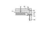
- FIG. 2 is an enlarged cross-sectional view showing an example of a detailed structure in the vicinity of the outer periphery of the shower head.
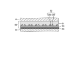
- FIG. 3 is a cross-sectional view showing an example of the structure of an EAG sheet.
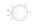
- FIG. 4 is a plan view showing an example of the arrangement of flow paths in a cooling plate.
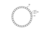
- FIG. 5 is a plan view showing an example of an arrangement of electrode pairs.
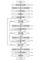
- FIG. 6 is a flow chart showing an example of a processing method.
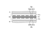
- FIG. 7 is a cross-sectional view showing another example of the structure of the EAG sheet.
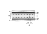
- FIG. 8 is a cross-sectional view showing another example of the structure of the EAG sheet.
- FIG. 1 is a schematic diagram showing an example of a plasma processing apparatus.
- FIG. 2 is an enlarged cross-sectional view showing an example of a detailed structure in the vicinity of the outer periphery of the shower head.
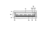
- FIG. 9 is a cross-sectional view showing another example of the structure of the EAG sheet.
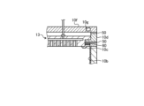
- FIG. 10 is an enlarged cross-sectional view showing another example of the detailed structure of the vicinity of the outer periphery of the shower head.
- FIG. 11 is a flowchart showing another example of the processing method.
- the heat transfer coefficient may differ from one location to another depending on the state of the contact surface.
- the state of the contact surface may change due to temperature changes or changes over time in the components, which may further change the heat transfer coefficient.
- the present disclosure therefore provides technology that can precisely control the temperature distribution of components.
- FIG. 1 is a diagram for explaining an example of the configuration of a capacitively coupled plasma processing apparatus 1.
- the plasma processing apparatus 1 is an example of a processing apparatus.
- the plasma processing system includes a capacitively coupled plasma processing device 1 and a control unit 2.
- the capacitively coupled plasma processing device 1 includes a plasma processing chamber 10, a gas supply unit 20, a power supply 30, and an exhaust system 40.
- the plasma processing chamber 10 is an example of a processing vessel.
- the plasma processing device 1 also includes a substrate support unit 11 and a gas introduction unit.
- the gas introduction unit is configured to introduce at least one processing gas into the plasma processing chamber 10.
- the gas introduction unit includes a shower head 13.
- the substrate support unit 11 is disposed in the plasma processing chamber 10.
- the shower head 13 is disposed above the substrate support unit 11. In one embodiment, the shower head 13 constitutes at least a part of the ceiling of the plasma processing chamber 10.
- the plasma processing chamber 10 has a plasma processing space 10s defined by the shower head 13, the sidewall 10a of the plasma processing chamber 10, and the substrate support unit 11.
- the plasma processing chamber 10 has at least one gas supply port for supplying at least one processing gas to the plasma processing space 10s and at least one gas exhaust port for exhausting gas from the plasma processing space.
- the plasma processing chamber 10 is grounded.
- the showerhead 13 and the substrate support 11 are electrically insulated from the housing of the plasma processing chamber 10.
- the substrate support 11 includes a main body 111 and a ring assembly 112.
- the main body 111 has a central region 111a for supporting the substrate W and an annular region 111b for supporting the ring assembly 112.
- a wafer is an example of a substrate W.
- the annular region 111b of the main body 111 surrounds the central region 111a of the main body 111 in a plan view.
- the substrate W is disposed on the central region 111a of the main body 111
- the ring assembly 112 is disposed on the annular region 111b of the main body 111 so as to surround the substrate W on the central region 111a of the main body 111. Therefore, the central region 111a is also called a substrate support surface for supporting the substrate W, and the annular region 111b is also called a ring support surface for supporting the ring assembly 112.
- the main body 111 includes a base 1110 and an electrostatic chuck 1111.
- the base 1110 includes a conductive member.
- the conductive member of the base 1110 may function as a lower electrode.
- the electrostatic chuck 1111 is disposed on the base 1110.
- the electrostatic chuck 1111 includes a ceramic member 1111a and an electrostatic electrode 1111b disposed within the ceramic member 1111a.
- the ceramic member 1111a has a central region 111a. In one embodiment, the ceramic member 1111a also has an annular region 111b. Note that other members surrounding the electrostatic chuck 1111, such as an annular electrostatic chuck or an annular insulating member, may have the annular region 111b.
- the ring assembly 112 may be disposed on the annular electrostatic chuck or the annular insulating member, or may be disposed on both the electrostatic chuck 1111 and the annular insulating member.
- at least one RF/DC electrode coupled to an RF (Radio Frequency) power source 31 and/or a DC (Direct Current) power source 32 described later may be disposed within the ceramic member 1111a.
- the at least one RF/DC electrode functions as a lower electrode.
- the RF/DC electrode is also called a bias electrode.
- the conductive member of the base 1110 and the at least one RF/DC electrode may function as multiple lower electrodes.
- the electrostatic electrode 1111b may function as a lower electrode.
- the substrate support 11 includes at least one lower electrode.
- the ring assembly 112 includes one or more annular members.
- the one or more annular members include one or more edge rings and at least one cover ring.
- the edge rings are formed of a conductive or insulating material, and the cover rings are formed of an insulating material.
- the substrate support 11 may also include a temperature adjustment module configured to adjust at least one of the electrostatic chuck 1111, the ring assembly 112, and the substrate to a target temperature.
- the temperature adjustment module may include a heater, a heat transfer fluid, a flow passage 1110a, or a combination thereof.
- a heat transfer fluid such as brine or a gas flows through the flow passage 1110a.
- the flow passage 1110a is formed in the base 1110, and one or more heaters are disposed in the ceramic member 1111a of the electrostatic chuck 1111.
- the substrate support 11 may also include a heat transfer gas supply configured to supply a heat transfer gas to a gap between the back surface of the substrate W and the central region 111a.
- a shower head 13 is provided on the upper part of the plasma processing chamber 10.
- the shower head 13 is supported by a support member 10d provided on the side wall 10a of the plasma processing chamber 10.
- a cooling plate 10f is provided above the shower head 13.
- the cooling plate 10f has a flow path 10g through which a heat transfer fluid such as brine or gas flows.
- a deposit shield 10b and a member 10c are provided below the support member 10d.
- the deposit shield 10b covers the side wall 10a and prevents reaction by-products (so-called deposits) generated by processing in the plasma processing space 10s from adhering to the side wall 10a.
- the member 10c is formed of a conductive member such as silicon, and is disposed on the lower surface of the shower head 13 along the outer periphery of the shower head 13.
- the member 10c is grounded.
- the member 10c and the deposit shield 10b are heated by the plasma generated in the plasma processing space 10s.
- the shower head 13 is configured to introduce at least one processing gas from the gas supply unit 20 into the plasma processing space 10s.
- the shower head 13 has at least one gas supply port 13a, at least one gas diffusion chamber 13b, and multiple gas inlets 13c.
- the processing gas supplied to the gas supply port 13a passes through the gas diffusion chamber 13b and is introduced into the plasma processing space 10s from the multiple gas inlets 13c.
- the shower head 13 also includes at least one upper electrode.
- the gas introduction unit may include, in addition to the shower head 13, one or more side gas injectors (SGIs) attached to one or more openings formed in the sidewall 10a.
- SGIs side gas injectors
- the gas supply 20 may include at least one gas source 21 and at least one flow controller 22.
- the gas supply 20 is configured to supply at least one process gas from a respective gas source 21 through a respective flow controller 22 to the showerhead 13.
- Each flow controller 22 may include, for example, a mass flow controller or a pressure-controlled flow controller.
- the gas supply 20 may include one or more flow modulation devices to modulate or pulse the flow rate of the at least one process gas.
- the power supply 30 includes an RF power supply 31 coupled to the plasma processing chamber 10 via at least one impedance matching circuit.
- the RF power supply 31 is configured to supply at least one RF signal (RF power) to at least one lower electrode and/or at least one upper electrode. This causes a plasma to be formed from at least one processing gas supplied to the plasma processing space 10s.
- the RF power supply 31 can function as at least a part of a plasma generating unit configured to generate plasma from one or more processing gases in the plasma processing chamber 10.
- a bias RF signal to the at least one lower electrode, a bias potential is generated on the substrate W, and ion components in the formed plasma can be attracted to the substrate W.
- the RF power supply 31 includes a first RF generating unit 31a and a second RF generating unit 31b.
- the first RF generating unit 31a is coupled to at least one lower electrode and/or at least one upper electrode via at least one impedance matching circuit and configured to generate a source RF signal (source RF power) for plasma generation.
- the source RF signal has a frequency in the range of 10 MHz to 150 MHz.
- the first RF generating unit 31a may be configured to generate multiple source RF signals having different frequencies. The generated one or more source RF signals are supplied to at least one lower electrode and/or at least one upper electrode.
- the second RF generator 31b is coupled to at least one lower electrode via at least one impedance matching circuit and configured to generate a bias RF signal (bias RF power).
- the frequency of the bias RF signal may be the same as or different from the frequency of the source RF signal.
- the bias RF signal has a lower frequency than the frequency of the source RF signal.
- the bias RF signal has a frequency in the range of 100 kHz to 60 MHz.
- the second RF generator 31b may be configured to generate multiple bias RF signals having different frequencies.
- the generated one or more bias RF signals are provided to at least one lower electrode. Also, in various embodiments, at least one of the source RF signal and the bias RF signal may be pulsed.
- the power supply 30 may also include a DC power supply 32 coupled to the plasma processing chamber 10.
- the DC power supply 32 includes a first DC generator 32a and a second DC generator 32b.
- the first DC generator 32a is connected to at least one lower electrode and configured to generate a first DC signal.
- the generated first bias DC signal is applied to the at least one lower electrode.
- the second DC generator 32b is connected to at least one upper electrode and configured to generate a second DC signal.
- the generated second DC signal is applied to the at least one upper electrode.
- At least one of the first and second DC signals may be pulsed.
- a sequence of voltage pulses is applied to at least one lower electrode and/or at least one upper electrode.
- the voltage pulses may have a rectangular, trapezoidal, triangular or combination thereof pulse waveform.
- a waveform generator for generating a sequence of voltage pulses from the DC signal is connected between the first DC generator 32a and at least one lower electrode.
- the first DC generator 32a and the waveform generator constitute a voltage pulse generator.
- the second DC generator 32b and the waveform generator constitute a voltage pulse generator
- the voltage pulse generator is connected to at least one upper electrode.
- the voltage pulses may have a positive polarity or a negative polarity.
- the sequence of voltage pulses may also include one or more positive polarity voltage pulses and one or more negative polarity voltage pulses within one period.
- the first and second DC generating units 32a and 32b may be provided in addition to the RF power source 31, or the first DC generating unit 32a may be provided in place of the second RF generating unit 31b.
- the exhaust system 40 may be connected to, for example, a gas exhaust port 10e provided at the bottom of the plasma processing chamber 10.
- the exhaust system 40 may include a pressure regulating valve and a vacuum pump. The pressure in the plasma processing space 10s is adjusted by the pressure regulating valve.
- the vacuum pump may include a turbomolecular pump, a dry pump, or a combination thereof.
- the control unit 2 processes computer-executable instructions that cause the plasma processing apparatus 1 to perform the various steps described in this disclosure.
- the control unit 2 may be configured to control each element of the plasma processing apparatus 1 to perform the various steps described herein. In one embodiment, a part or all of the control unit 2 may be included in the plasma processing apparatus 1.
- the control unit 2 may include a processing unit 2a1, a storage unit 2a2, and a communication interface 2a3.
- the control unit 2 is realized, for example, by a computer 2a.
- the processing unit 2a1 may be configured to perform various control operations by reading a program from the storage unit 2a2 and executing the read program. This program may be stored in the storage unit 2a2 in advance, or may be acquired via a medium when necessary.
- the acquired program is stored in the storage unit 2a2 and is read from the storage unit 2a2 by the processing unit 2a1 and executed.
- the medium may be various storage media readable by the computer 2a, or may be a communication line connected to the communication interface 2a3.
- the processing unit 2a1 may be a CPU (Central Processing Unit).
- the memory unit 2a2 may include a RAM (Random Access Memory), a ROM (Read Only Memory), a HDD (Hard Disk Drive), an SSD (Solid State Drive), or a combination of these.
- the communication interface 2a3 may communicate with the plasma processing device 1 via a communication line such as a LAN (Local Area Network).
- [Upper Structure of Plasma Processing Chamber 10] 2 is an enlarged cross-sectional view showing an example of a detailed structure near the outer periphery of the shower head 13.
- EAG sheets 50 are arranged between the cooling plate 10f and the support member 10d, between the support member 10d and the deposit shield 10b, and between the support member 10d and the member 10c.
- the cooling plate 10f exchanges heat with the support member 10d through the EAG sheet 50 to cool the support member 10d.
- the support member 10d exchanges heat with the deposit shield 10b and the member 10c through the EAG sheet 50 to cool the deposit shield 10b and the member 10c.
- the cooling plate 10f is an example of a first member
- the support member 10d is an example of a second member
- the support member 10d is an example of a first member
- the deposit shield 10b and member 10c are an example of a second member.
- the EAG sheet 50 has an ER (Electro-Rheological) gel 51, multiple electrode pairs 52, and a substrate 53.
- the ER gel 51 is an example of an EAG layer.
- Each electrode pair 52 has an electrode 520 and an electrode 521, and is disposed on the surface of the substrate 53.
- the electrode pair 52 and the ER gel 51 are disposed on one side of the substrate 53, the ER gel 51 in the EAG sheet 50 is disposed on the component A side, and the substrate 53 is disposed on the component B side.
- a voltage controlled by the control unit 2 is applied between the electrodes 520 and 521.
- the thermal conductivity of the ER gel 51 in the vicinity of the electrodes 520 and 521 changes depending on the magnitude of the voltage applied between the electrodes 520 and 521.
- the magnitude of the voltage applied between the electrodes 520 and 521 is controlled independently for each electrode pair 52. By controlling the voltage applied to each electrode pair 52, the thermal conductivity between member A and member B via the ER gel 51 in the vicinity of the electrode pair 52 can be individually controlled.
- a thermally conductive sheet 54 having high thermal conductivity and elasticity is placed between the substrate 53 and the member B.
- An example of such a thermally conductive sheet 54 is a conductive metal foil tape in which metal particles such as gold, silver, copper, or aluminum are dispersed in an adhesive resin such as epoxy.
- an adhesive using, for example, a metal paste adhesive such as gold, silver, copper, or aluminum, heat-resistant rubber (mainly composed of organic polymers such as natural rubber or synthetic rubber), silicone rubber, silicon, or the like may be placed.
- the substrate 53 can be made of an insulating material such as a resin film, such as polyimide or polyethylene terephthalate, a resin plate, such as glass, epoxy resin or phenolic resin, or a ceramic, such as alumina.
- the substrate 53 is preferably made of a material with high thermal conductivity.
- ER gel 51 contains gel and fine particles.
- gels include silicone gel, silicone oil, and mineral oil.
- Silicone gel is, for example, made by mixing ER fluid with two types of gelling agents and a catalyst, and then gelling it through a heat treatment.
- fine particles examples include inorganic-organic composite fine particles with an acrylic polymer core and coated with tin oxide, silica particles, polymer electrolyte particles, conductive polymer particles, conductive polymer particles with coated surfaces, sodium polymethacrylate particles, lithium polymethacrylate, cellulose, zeolite, carbon, polyaniline, etc.
- the thermal conductivity of the ER gel 51 can be improved.
- three-dimensional microstructures formed by a 3D printer, photolithography, or the like may be added to the ER gel 51.
- the heat transfer coefficient may differ from one location to another on the contact surface depending on the state of the contact surface.
- the state of the contact surface may also change due to temperature changes and changes over time in members A and B, which may further change the heat transfer coefficient.
- the state of the contact surface and changes in the state of the contact surface may differ from device to device.
- a gel-like ER gel 51 is placed between member A and substrate 53, and an elastic heat conductive sheet 54 is placed between substrate 53 and member B.
- a gel-like ER gel 51 is placed between member A and substrate 53, and an elastic heat conductive sheet 54 is placed between substrate 53 and member B.
- the ER gel 51 and heat conductive sheet 54 deform in response to the deformation of members A and B.
- FIG. 4 is a plan view showing an example of the arrangement of the flow paths 10g in the cooling plate 10f.
- the flow paths 10g are indicated by dashed lines.
- a temperature-controlled heat transfer fluid is supplied into the cooling plate 10f from a temperature control device such as a chiller unit (not shown).
- the heat transfer fluid supplied from the temperature control device enters the flow path 10g from the inlet 10g1 and flows through the flow path 10g.
- the heat transfer fluid flowing through the flow path 10g exchanges heat with the support member 10d via the cooling plate 10f and the EAG sheet 50, and is returned to the temperature control device from the outlet 10g2.
- the temperature of the cooling plate 10f in the region R2 near the outlet 10g2 may be higher than the temperature of the cooling plate 10f in the region R1 near the inlet 10g1. In that case, even if the temperature of the heat transfer fluid is controlled, a temperature gradient occurs in the cooling plate 10f along the flow of the heat transfer fluid, causing a bias in the temperature distribution of the cooling plate 10f. This also causes a bias in the temperature distribution of the support member 10d that exchanges heat with the cooling plate 10f.
- an EAG sheet 50 is placed between the cooling plate 10f and the support member 10d.
- a plurality of electrode pairs 52 are placed along the surface of the support member 10d on the cooling plate 10f side.
- the voltage applied to each electrode pair 52 is controlled so that the heat transfer coefficient of the ER gel 51 is low in the part of the cooling plate 10f where the temperature is relatively low, and is high in the part of the cooling plate 10f where the temperature is relatively high.
- the plasma processing chamber 10 there are parts that are heated to a predetermined temperature for the purpose of suppressing the adhesion of deposits during plasma processing. Some of these parts are heated by heat input from the plasma. Examples of such parts include the deposit shield 10b and member 10c (see Figure 2).
- an EAG sheet 50 is placed between the support member 10d and the deposit shield 10b, and between the support member 10d and the member 10c, to control the thermal conductivity between the support member 10d and the deposit shield 10b, and between the support member 10d and the member 10c.
- the voltage applied to the electrode pair 52 of the EAG sheet 50 is controlled so that the thermal conductivity between the support member 10d and the deposit shield 10b, and between the support member 10d and the member 10c is reduced. This allows the deposit shield 10b and the member 10c to be heated by heat input from the plasma, without using a heating means such as a heater.
- the deposit shield 10b and the member 10c are provided with temperature sensors (not shown).
- the voltage applied to the electrode pair 52 of the EAG sheet 50 is controlled so that the heat transfer coefficient between the support member 10d and the deposit shield 10b, and between the support member 10d and the member 10c, is increased. This allows the temperature of the deposit shield 10b and the member 10c to be lowered by heat exchange with the support member 10d.
- the voltage applied to the electrode pair 52 of the EAG sheet 50 is controlled so that the heat transfer coefficient between the support member 10d and the deposit shield 10b, and between the support member 10d and the member 10c, is increased. This allows the temperature of the deposit shield 10b and the member 10c to be reduced quickly.
- the EAG sheet 50 arranged between the support member 10d and the deposit shield 10b, and between the support member 10d and the member 10c, has multiple electrode pairs 52 arranged along the extension direction of the EAG sheet 50, similar to the EAG sheet 50 shown in FIG. 5, for example.
- the EAG sheet 50 arranged between the support member 10d and the deposit shield 10b, and between the support member 10d and the member 10c may have one electrode pair 52 arranged along the extension direction of the EAG sheet 50.
- FIG. 6 is a flow chart showing an example of a processing method. Each step shown in Fig. 6 is realized by the control unit 2 controlling each part of the plasma processing apparatus 1. Note that the flow chart shown in Fig. 6 describes, as an example, the control of the EAG sheet 50 arranged between the cooling plate 10f and the support member 10d, between the support member 10d and the deposit shield 10b, and between the support member 10d and the member 10c.
- Step S10 is an example of process a).
- the voltage applied to each electrode pair 52 included in the EAG sheet 50 arranged between the cooling plate 10f and the support member 10d is individually controlled so as to reduce the bias of the temperature distribution in the support member 10d.
- step S11 the thermal conductivity of the EAG sheet 50 arranged between the support member 10d and the deposit shield 10b, and between the support member 10d and the member 10c, is controlled to be small (step S11).
- step S11 the voltage applied to the electrode pair 52 of the EAG sheet 50 arranged between the support member 10d and the deposit shield 10b, and between the support member 10d and the member 10c is controlled to be, for example, a minimum (for example, 0 V).
- step S12 the substrate W to be processed is loaded into the plasma processing chamber 10 (step S12).
- a gate valve (not shown) provided on the sidewall 10a of the plasma processing chamber 10 is opened, and the substrate W is loaded into the plasma processing chamber 10 by a transfer robot (not shown).
- the substrate W is then handed over to lift pins (not shown) protruding from the upper surface of the electrostatic chuck 1111.
- the lift pins (not shown) are then lowered by driving a lifting mechanism (not shown), and the substrate W is placed on the upper surface of the electrostatic chuck 1111.
- the lifting mechanism (not shown) is controlled by the controller 2.
- Step S13 is an example of process b).
- processing gas is supplied from the gas supply unit 20 into the plasma processing chamber 10 via the shower head 13.
- the pressure inside the plasma processing chamber 10 is then adjusted to a predetermined value by the exhaust system 40.
- RF power is then supplied from the power source 30 into the plasma processing chamber 10, whereby the processing gas in the plasma processing chamber 10 is converted into plasma, and plasma is generated in the plasma processing chamber 10.
- the plasma generated in the plasma processing chamber 10 then performs processing such as etching on the substrate W.
- the member 10c and the deposit shield 10b are heated by the plasma generated in the plasma processing space 10s, suppressing the adhesion of deposits to the member 10c and the deposit shield 10b.
- the thermal conductivity of the EAG sheet 50 arranged between the support member 10d and the deposit shield 10b, and between the support member 10d and the member 10c, is controlled to be small. Therefore, the member 10c and the deposit shield 10b are efficiently heated by the plasma generated in the plasma processing space 10s.
- step S14 it is determined whether the temperature of the members in the plasma processing chamber 10 is equal to or higher than a predetermined first temperature.
- the members in the plasma processing chamber 10 are, for example, the deposit shield 10b and member 10c. If the temperature of the members in the plasma processing chamber 10 is less than the first temperature (step S14: No), the process shown in step S16 is executed.
- step S15 is an example of process d). This promotes heat exchange between, for example, the deposit shield 10b and member 10c and the support member 10d, lowering the temperatures of the deposit shield 10b and member 10c. This makes it possible to prevent overheating of the deposit shield 10b and member 10c.
- step S16 it is determined whether the temperature of the members in the plasma processing chamber 10 is equal to or lower than a predetermined second temperature.
- the second temperature is a temperature lower than the first temperature. If the temperature of the members in the plasma processing chamber 10 is higher than the second temperature (step S16: No), the process shown in step S18 is executed.
- step S16 if the temperature of the member in the plasma processing chamber 10 falls below the second temperature (step S16: Yes), the voltage applied to the electrode pair 52 of the EAG sheet 50 is controlled so that the thermal conductivity of the EAG sheet 50 is reduced (step S17).
- Step S17 is an example of process c). This suppresses heat exchange between, for example, the deposit shield 10b and member 10c and the support member 10d, and the temperatures of the deposit shield 10b and member 10c rise due to heat input from the plasma.
- the temperatures of, for example, the deposit shield 10b and member 10c can be maintained between the first temperature and the second temperature.
- step S18 it is determined whether or not to end the processing of the substrate W (step S18). If the processing of the substrate W is not to be ended (step S18: No), the processing shown in step S14 is executed again.
- step S18 when the processing of the substrate W is to be terminated (step S18: Yes), the thermal conductivity between the support member 10d and the deposit shield 10b, and between the support member 10d and the member 10c is controlled to be increased (step S19).
- Step S19 is an example of process e).
- the voltage applied to the electrode pair 52 of the EAG sheet 50 arranged between the support member 10d and the deposit shield 10b, and between the support member 10d and the member 10c is controlled to be, for example, maximum. This allows the temperature of the deposit shield 10b and the member 10c to be quickly reduced.
- step S20 the substrate W is removed (step S20).
- step S20 the substrate W is lifted by lift pins (not shown) driven by a lifting mechanism (not shown). Then, a gate valve (not shown) is opened, and the substrate W is removed from the plasma processing chamber 10 by a transfer robot (not shown). Then, the process shown in this flowchart is completed.
- the processing apparatus in this embodiment includes a first member (cooling plate 10f), a second member (support member 10d), an EAG (Electro-Adhesive Gel) sheet (EAG sheet 50) disposed between the first member and the second member, and a control unit (control unit 2).
- the EAG sheet includes an EAG layer (ER gel 51), a plurality of electrode pairs (electrode pair 52) having two electrodes (electrode 520 and electrode 521), and a substrate (substrate 53) on which the plurality of electrode pairs are disposed.
- the control unit independently controls the thermal conductivity of the EAG layer near each of the plurality of electrode pairs by independently controlling the voltages applied to each of the plurality of electrode pairs so that the temperature distribution of the first member or the second member becomes a predetermined temperature distribution by heat exchange between the first member and the second member. This allows the temperature distribution of the member to be controlled with precision.
- the electrode pair and EAG layer are arranged on one side of the substrate, the EAG layer of the EAG sheet is arranged on the first member side, and the substrate is arranged on the second member side. This can improve the adhesion between the first member and the EAG sheet.
- a sheet or adhesive having high thermal conductivity, elasticity, and electrical conductivity is placed between the substrate and the second member. This can improve the adhesion between the second member and the substrate of the EAG sheet.
- a temperature-controlled heat transfer fluid flows inside the first member, and the first member exchanges heat with the second member via the EAG sheet. Even if a bias in the temperature distribution of the first member occurs due to a temperature change in the heat transfer fluid, the bias in the temperature distribution of the second member can be suppressed by independently controlling the voltages applied to each of the multiple electrode pairs.
- the processing apparatus in the above embodiment further includes a processing vessel (plasma processing chamber 10) that processes a wafer (substrate W) using plasma generated inside.
- the second member is heated by heat input from the plasma in the processing vessel.
- the control unit controls the voltage applied to the electrode pair so that the thermal conductivity of the EAG sheet is increased. This makes it possible to prevent overheating of the second member.
- control unit controls the voltage applied to the electrode pair so that the thermal conductivity of the EAG sheet decreases when the temperature of the second member becomes equal to or lower than a second temperature that is lower than the first temperature.
- control unit controls the voltage applied to the electrode pair so that the thermal conductivity of the EAG sheet is increased. This allows the temperature of the second member to be quickly reduced.
- the processing apparatus in the above embodiment further includes a shower head 13.
- the first member and the second member are provided around the shower head 13. This allows the temperature distribution of the members around the shower head 13 to be precisely controlled.
- the above-mentioned embodiment is a processing method in a processing apparatus.
- the processing apparatus includes a first member, a second member, an EAG (Electro-Adhesive Gel) sheet disposed between the first member and the second member, a processing vessel for processing a wafer using plasma generated inside, and a control unit.
- the EAG sheet includes an EAG layer, a plurality of electrode pairs each having two electrodes, and a substrate on which the plurality of electrode pairs are disposed.
- the control unit executes step a).
- step a) the voltages applied to each of the plurality of electrode pairs are independently controlled so that the temperature distribution of the first member or the second member becomes a predetermined temperature distribution by heat exchange between the first member and the second member, thereby independently controlling the thermal conductivity of the EAG layer near each of the plurality of electrode pairs. This allows the temperature distribution of the member to be precisely controlled.
- a temperature-controlled heat transfer fluid flows inside the first member, and the second member exchanges heat with the first member via the EAG sheet, and is heated by heat input from the plasma in the processing vessel.
- the control unit further executes steps b) and c).
- step b) plasma is generated in the processing vessel.
- step c) while plasma is being generated in the processing vessel, the voltage applied to the electrode pair is controlled so that the thermal conductivity of the EAG sheet is reduced. This allows the second member to be efficiently heated by the plasma generated in the processing vessel, without the need for a heater to heat the second member.
- control unit further executes step d).
- step d when the temperature of the second member reaches a predetermined temperature, the voltage applied to the electrode pair is controlled so that the thermal conductivity of the EAG sheet is increased. This makes it possible to prevent overheating of the second member.
- control unit further executes step e).
- step e when the generation of plasma in the processing vessel is completed, the voltage applied to the electrode pair is controlled so that the thermal conductivity of the EAG sheet is increased. This allows the temperature of the second member to be quickly reduced.
- the EAG sheet 50 has the ER gel 51 and the electrode pair 52 arranged on one side of the substrate 53, but the disclosed technology is not limited to this.
- the ER gel 51 and the electrode pair 52 may be arranged on both sides of the substrate 53.
- FIG. 7 is a cross-sectional view showing another example of the structure of the EAG sheet 50.
- the EAG sheet 50 illustrated in FIG. 7 has ER gel 51a, ER gel 51b, electrode pair 52a, electrode pair 52b, and substrate 53.
- Electrode pair 52a includes electrode 520a and electrode 521a.
- Electrode pair 52b includes electrode 520b and electrode 521b.
- ER gel 51a and electrode pair 52a are disposed on one side of substrate 53, and ER gel 51b and electrode pair 52b are disposed on the other side of substrate 53.
- Electrode pair 52a is an example of a first electrode pair, and electrode pair 52b is an example of a second electrode pair.
- ER gel 51a is an example of a first EAG layer
- ER gel 51b is an example of a second EAG layer.
- the EAG sheet 50 may have a structure in which the ER gel 51 is sandwiched between two substrates 53, as shown in FIG. 8, for example.
- FIG. 8 is a cross-sectional view showing another example of the structure of the EAG sheet 50.
- the EAG sheet 50 shown in FIG. 8 has an ER gel 51, an electrode pair 52, a substrate 53a, a substrate 53b, a thermally conductive sheet 54a, and a thermally conductive sheet 54b.
- the ER gel 51 is disposed between the substrate 53a and the substrate 53b.
- the electrode pair 52 includes an electrode 520 and an electrode 521, the electrode 520 being disposed on the substrate 53a, and the electrode 521 being disposed on the substrate 53b.
- one electrode included in the electrode pair 52 is disposed on the surface of the substrate 53a on the ER gel 51 side, and the other electrode included in each electrode pair 52 is disposed on the surface of the substrate 53b on the ER gel 51 side.
- a thermally conductive sheet 54a is disposed between member A and substrate 53a, and a thermally conductive sheet 54b is disposed between member B and substrate 53b. Note that instead of thermally conductive sheets 54a and 54b, an adhesive with high thermal conductivity may be disposed.
- Substrate 53a is an example of a first substrate
- substrate 53b is an example of a second substrate.
- a low thermal conductive member 55 may be arranged at the end of the ER gel 51, as shown in FIG. 9.
- the low thermal conductive member 55 is formed of, for example, heat-resistant rubber (mainly composed of organic polymers such as natural rubber or synthetic rubber), resin (member made of polymer compounds such as epoxy resin), ceramic (alumina, zirconia), quartz, SUS (Steel Use Stainless) material, Hastelloy (registered trademark), titanium, Zircaloy, etc.
- FIG. 10 is an enlarged cross-sectional view showing another example of a detailed structure near the outer periphery of the shower head 13. This allows the temperatures of the deposit shield 10b and the member 10c to be heated to a predetermined temperature before plasma is generated in the plasma processing chamber 10. Note that, after plasma is generated in the plasma processing chamber 10, the power supply to the heater 60 may be stopped.
- FIG. 11 is a flow chart showing another example of a processing method.
- the processing illustrated in FIG. 11 is performed by a plasma processing apparatus 1 having the structure illustrated in FIG. 10. Note that, except for the points described below, the processing in FIG. 11 that is given the same reference numerals as in FIG. 6 is the same as the processing described in FIG. 6, and therefore the description thereof will be omitted.
- step S11 the thermal conductivity of the EAG sheet 50 arranged between the support member 10d and the deposit shield 10b, and between the support member 10d and the member 10c is controlled to be small, and then power is supplied to the heater 60 (step S30). This allows the temperature of the deposit shield 10b and the member 10c to be quickly heated to a predetermined temperature.
- step S15 the thermal conductivity of the EAG sheet 50 arranged between the support member 10d and the deposit shield 10b, and between the support member 10d and the member 10c is controlled to be large, and then the power supply to the heater 60 is stopped (step S31). This allows the temperature of the deposit shield 10b and the member 10c to be quickly reduced.
- step S17 the thermal conductivity of the EAG sheet 50 arranged between the support member 10d and the deposit shield 10b, and between the support member 10d and the member 10c is controlled to be small, and then power is supplied to the heater 60 again (step S32).
- step S32 the thermal conductivity of the EAG sheet 50 arranged between the support member 10d and the deposit shield 10b, and between the support member 10d and the member 10c is controlled to be small, and then power is supplied to the heater 60 again (step S32).
- step S32 the thermal conductivity of the EAG sheet 50 arranged between the support member 10d and the deposit shield 10b, and between the support member 10d and the member 10c is controlled to be small, and then power is supplied to the heater 60 again (step S32).
- step S19 the thermal conductivity of the EAG sheet 50 arranged between the support member 10d and the deposit shield 10b, and between the support member 10d and the member 10c is controlled to be increased, and then the power supply to the heater 60 is stopped (step S33). This allows the temperature of the deposit shield 10b and the member 10c to be quickly reduced.
- the EAG sheet 50 is disposed between the cooling plate 10f and the support member 10d, between the support member 10d and the deposit shield 10b, and between the support member 10d and the member 10c, but the disclosed technology is not limited to this.
- the EAG sheet 50 may be disposed between two other members, such as between the electrostatic chuck 1111 and the base 1110, or between the electrostatic chuck 1111 and the ring assembly 112, as long as the two members have heat transfer.
- the plasma processing apparatus 1 is described as performing processing using a capacitively coupled plasma (CCP) as an example of a plasma source, but the plasma source is not limited to this.
- plasma sources other than capacitively coupled plasma include inductively coupled plasma (ICP), microwave excited surface wave plasma (SWP), electron cyclotron resonance plasma (ECP), and helicon wave excited plasma (HWP).
- the EAG sheet is An EAG layer; A plurality of electrode pairs each having two electrodes; a substrate on which a plurality of the electrode pairs are disposed;
- the control unit is A processing device that independently controls the thermal conductivity of the EAG layer in the vicinity of each of the multiple electrode pairs by independently controlling the voltages applied to each of the multiple electrode pairs so that the temperature distribution of the first member or the second member becomes a predetermined temperature distribution due to heat exchange between the first member and the second member.
- the electrode pair and the EAG layer are disposed on one side of the substrate; 2.
- the processing apparatus wherein the EAG layer of the EAG sheet is disposed on the first member side, and the substrate is disposed on the second member side. (Appendix 3) 3. The processing apparatus according to claim 2, wherein a conductive sheet or adhesive is disposed between the substrate and the second member. (Appendix 4) the electrode pairs include a first electrode pair and a second electrode pair; the EAG layer includes a first EAG layer and a second EAG layer; The first electrode pair and the first EAG layer are disposed on one side of the substrate; the second electrode pair and the second EAG layer are disposed on the other side of the substrate; 2. The processing device of claim 1, wherein the first EAG layer is disposed on the first member side and the second EAG layer is disposed on the second member side.
- the substrate includes a first substrate and a second substrate; the EAG layer is disposed between the first substrate and the second substrate; One electrode included in each of the electrode pairs is disposed on a surface of the first substrate on the EAG layer side, The processing device of claim 1, wherein the other electrode in each of the electrode pairs is positioned on the surface of the second substrate on the EAG layer side.
- the first substrate is disposed on the first member side, the second substrate is disposed on the second member side,
- the processing apparatus of claim 5, wherein a conductive and elastic sheet or adhesive is disposed between the first substrate and the first member, and between the second substrate and the second member.
- a temperature-controlled heat transfer fluid flows inside the first member, 7.
- the processing apparatus according to claim 1, wherein the first member exchanges heat with the second member via the EAG sheet.
- Appendix 8 a processing vessel for processing the wafer using the plasma generated therein; the second member is heated by heat input from plasma in the processing chamber; The processing apparatus described in Appendix 7, wherein the control unit controls the voltage applied to the electrode pair so as to increase the thermal conductivity of the EAG sheet when plasma is generated in the processing container and the temperature of the second member is equal to or higher than a predetermined first temperature.
- Appendix 9 The processing device described in Appendix 8, wherein the control unit controls the voltage applied to the electrode pair so that the thermal conductivity of the EAG sheet is reduced when the temperature of the second member becomes lower than a second temperature that is lower than the first temperature.
- the apparatus includes a first member, a second member, an electro-adhesive gel (EAG) sheet disposed between the first member and the second member, a processing vessel for processing a wafer using plasma generated therein, and a control unit;
- the EAG sheet includes an EAG layer, a plurality of electrode pairs each having two electrodes, and a substrate on which the plurality of electrode pairs are disposed.
- the control unit a) a processing method for independently controlling the thermal conductivity of the EAG layer in the vicinity of each of a plurality of electrode pairs by independently controlling the voltages applied to each of the plurality of electrode pairs so that the temperature distribution of the first member or the second member becomes a predetermined temperature distribution due to heat exchange between the first member and the second member.
- a temperature-controlled heat transfer fluid flows inside the first member, the second member exchanges heat with the first member via the EAG sheet and is heated by heat input from plasma in the processing chamber;
- the control unit b) generating a plasma in the processing chamber; c) controlling the voltage applied to the electrode pair so as to reduce the thermal conductivity of the EAG sheet while plasma is being generated in the processing vessel.
- the control unit d) controlling the voltage applied to the electrode pair so as to increase the thermal conductivity of the EAG sheet when the temperature of the second member reaches a predetermined temperature.
- the control unit e) The processing method described in Appendix 14 or 15, further comprising the step of controlling the voltage applied to the electrode pair so as to increase the thermal conductivity of the EAG sheet when plasma generation in the processing vessel is terminated.
- Plasma processing apparatus 10 Plasma processing chamber 10a Side wall 10b Deposit shield 10c Member 10d Support member 10e Gas exhaust port 10f Cooling plate 10g Flow path 10g1 Inlet 10g2 Outlet 10s Plasma processing space 11 Substrate support portion 111 Main body portion 111a Central region 111b Annular region 1110 Base 1110a Flow path 1111 Electrostatic chuck 1111a Ceramic member 1111b Electrostatic electrode 112 Ring assembly 13 shower head 13a Gas supply port 13b Gas diffusion chamber 13c Gas inlet 20 Gas supply portion 21 Gas source 22 Flow rate controller 30 Power source 31 RF power source 31a First RF generator 31b Second RF generator 32 DC power source 32a First DC generator 32b Second DC generator 40 Exhaust system 2 Control unit 2a Computer 2a1 Processing unit 2a2 Storage unit 2a3 Communication interface 50 EAG sheet 51 ER gel 52 Electrode pair 520 Electrode 521 Electrode 53 Substrate 54 Thermally conductive sheet 55 Low thermally conductive member 60 Heater
Landscapes
- Physics & Mathematics (AREA)
- Engineering & Computer Science (AREA)
- Plasma & Fusion (AREA)
- Chemical & Material Sciences (AREA)
- Analytical Chemistry (AREA)
- Chemical Vapour Deposition (AREA)
- Plasma Technology (AREA)
- Dicing (AREA)
- Physical Or Chemical Processes And Apparatus (AREA)
Abstract
Description
以下に、プラズマ処理システムの構成例について説明する。図1は、容量結合型のプラズマ処理装置1の構成例を説明するための図である。プラズマ処理装置1は処理装置の一例である。
図2は、シャワーヘッド13の外周付近の詳細構造の一例を示す拡大断面図である。クーリングプレート10fと支持部材10dとの間、支持部材10dとデポシールド10bとの間、および、支持部材10dと部材10cとの間には、EAGシート50が配置されている。クーリングプレート10fは、EAGシート50を介して支持部材10dとの間で熱交換を行い、支持部材10dを冷却する。支持部材10dは、EAGシート50を介してデポシールド10bおよび部材10cとの間で熱交換を行い、デポシールド10bおよび部材10cを冷却する。クーリングプレート10fと支持部材10dとの関係では、クーリングプレート10fは第1の部材の一例であり、支持部材10dは第2の部材の一例である。また、支持部材10dと、デポシールド10bおよび部材10cとの関係では、支持部材10dは第1の部材の一例であり、デポシールド10bおよび部材10cは第2の部材の一例である。
図6は、処理方法の一例を示すフローチャートである。図6に例示された各ステップは、制御部2がプラズマ処理装置1の各部を制御することにより実現される。なお、図6に例示されたフローチャートでは、一例として、クーリングプレート10fと支持部材10dとの間、支持部材10dとデポシールド10bとの間、および支持部材10dと部材10cとの間に配置されたEAGシート50の制御を説明している。
なお、本願に開示された技術は、上記した実施形態に限定されるものではなく、その要旨の範囲内で数々の変形が可能である。
第1の部材と、
第2の部材と、
前記第1の部材と前記第2の部材の間に配置されるEAG(Electro-Adhesive Gel)シートと、
制御部と
を備え、
前記EAGシートは、
EAG層と、
2つの電極を有する複数の電極ペアと、
複数の前記電極ペアが配置される基板と
を有し、
前記制御部は、
前記第1の部材と前記第2の部材との間の熱交換により前記第1の部材または前記第2の部材の温度分布が予め定められた温度分布となるように、複数の前記電極ペアのそれぞれに印加する電圧を互いに独立に制御することにより、複数の前記電極ペアのそれぞれの近傍の前記EAG層の熱伝導率を独立に制御する処理装置。
(付記2)
前記基板の一方の面に前記電極ペアおよび前記EAG層が配置され、
前記EAGシートにおける前記EAG層が前記第1の部材側に配置され、前記基板が前記第2の部材側に配置される付記1に記載の処理装置。
(付記3)
前記基板と前記第2の部材との間には、導電性を有するシートまたは接着剤が配置される付記2に記載の処理装置。
(付記4)
前記電極ペアは、第1の電極ペアと第2の電極ペアとを含み、
前記EAG層は、第1のEAG層と第2のEAG層とを含み、
前記基板の一方の面に前記第1の電極ペアおよび前記第1のEAG層が配置され、
前記基板の他方の面に前記第2の電極ペアおよび前記第2のEAG層が配置され、
前記第1のEAG層が前記第1の部材側に配置され、前記第2のEAG層が前記第2の部材側に配置される付記1に記載の処理装置。
(付記5)
前記基板は、第1の基板および第2の基板を含み、
前記EAG層は、前記第1の基板と前記第2の基板の間に配置され、
それぞれの前記電極ペアに含まれる一方の電極は、前記EAG層側の前記第1の基板の面に配置され、
それぞれの前記電極ペアに含まれる他方の電極は、前記EAG層側の前記第2の基板の面に配置される付記1に記載の処理装置。
(付記6)
前記第1の基板が前記第1の部材側に配置され、
前記第2の基板が前記第2の部材側に配置され、
前記第1の基板と前記第1の部材との間、および、前記第2の基板と前記第2の部材との間には、導電性及び弾性を有するシートまたは接着剤が配置される付記5に記載の処理装置。
(付記7)
前記第1の部材の内部には温度制御された伝熱流体が流れ、
前記第1の部材は、前記EAGシートを介して前記第2の部材との間で熱交換を行う付記1から6のいずれか一つに記載の処理装置。
(付記8)
内部で生成されたプラズマを用いてウェハに対して処理を行う処理容器をさらに備え、
前記第2の部材は、前記処理容器内のプラズマからの入熱により加熱され、
前記制御部は、前記処理容器内でプラズマが生成されており、かつ、前記第2の部材の温度が予め定められた第1の温度以上の場合に、前記EAGシートの熱伝導率が大きくなるように前記電極ペアに印加される電圧を制御する付記7に記載の処理装置。
(付記9)
前記制御部は、前記第2の部材の温度が前記第1の温度よりの低い第2の温度以下になった場合に、前記EAGシートの熱伝導率が小さくなるように前記電極ペアに印加される電圧を制御する付記8に記載の処理装置。
(付記10)
前記制御部は、前記処理容器内でのプラズマの生成が終了した場合に、前記EAGシートの熱伝導率が大きくなるように前記電極ペアに印加される電圧を制御する付記8または9に記載の処理装置。
(付記11)
前記第2の部材の内部にはヒータが埋め込まれており、
前記制御部は、前記EAGシートの熱伝導率が小さくなるように前記電極ペアに印加される電圧を制御する際に、前記ヒータに電力を供給する付記8から10のいずれか一つに記載の処理装置。
(付記12)
シャワーヘッドをさらに備え、
前記第1の部材および前記第2の部材は、前記シャワーヘッドの周囲に設けられる付記1から11のいずれか一つに記載の処理装置。
(付記13)
第1の部材と、第2の部材と、前記第1の部材と前記第2の部材の間に配置されるEAG(Electro-Adhesive Gel)シートと、内部で生成されたプラズマを用いてウェハに対して処理を行う処理容器と、制御部とを備え、
前記EAGシートは、EAG層と、2つの電極を有する複数の電極ペアと、複数の前記電極ペアが配置される基板とを有し、
前記制御部が、
a)前記第1の部材と前記第2の部材との間の熱交換により前記第1の部材または前記第2の部材の温度分布が予め定められた温度分布となるように、複数の前記電極ペアのそれぞれに印加する電圧を互いに独立に制御することにより、複数の前記電極ペアのそれぞれの近傍の前記EAG層の熱伝導率を独立に制御する工程
を実行する処理方法。
(付記14)
前記第1の部材の内部には温度制御された伝熱流体が流れ、
前記第2の部材は、前記EAGシートを介して前記第1の部材との間で熱交換を行うと共に、前記処理容器内のプラズマからの入熱により加熱され、
前記制御部が、
b)前記処理容器内でプラズマを生成する工程と、
c)前記処理容器内でプラズマが生成されている状態で、前記EAGシートの熱伝導率が小さくなるように前記電極ペアに印加される電圧を制御する工程と
をさらに実行する付記13に記載の処理方法。
(付記15)
前記制御部が、
d)前記第2の部材の温度が予め定められた温度に達した場合に、前記EAGシートの熱伝導率が大きくなるように前記電極ペアに印加される電圧を制御する工程
をさらに実行する付記14に記載の処理方法。
(付記16)
前記制御部が、
e)前記処理容器内でのプラズマの生成が終了した場合に、前記EAGシートの熱伝導率が大きくなるように前記電極ペアに印加される電圧を制御する工程
をさらに実行する付記14または15に記載の処理方法。
W 基板
1 プラズマ処理装置
10 プラズマ処理チャンバ
10a 側壁
10b デポシールド
10c 部材
10d 支持部材
10e ガス排出口
10f クーリングプレート
10g 流路
10g1 入口
10g2 出口
10s プラズマ処理空間
11 基板支持部
111 本体部
111a 中央領域
111b 環状領域
1110 基台
1110a 流路
1111 静電チャック
1111a セラミック部材
1111b 静電電極
112 リングアセンブリ
13 シャワーヘッド
13a ガス供給口
13b ガス拡散室
13c ガス導入口
20 ガス供給部
21 ガスソース
22 流量制御器
30 電源
31 RF電源
31a 第1のRF生成部
31b 第2のRF生成部
32 DC電源
32a 第1のDC生成部
32b 第2のDC生成部
40 排気システム
2 制御部
2a コンピュータ
2a1 処理部
2a2 記憶部
2a3 通信インターフェース
50 EAGシート
51 ERゲル
52 電極ペア
520 電極
521 電極
53 基板
54 熱伝導シート
55 低熱伝導部材
60 ヒータ
Claims (16)
- 第1の部材と、
第2の部材と、
前記第1の部材と前記第2の部材の間に配置されるEAG(Electro-Adhesive Gel)シートと、
制御部と
を備え、
前記EAGシートは、
EAG層と、
2つの電極を有する複数の電極ペアと、
複数の前記電極ペアが配置される基板と
を有し、
前記制御部は、
前記第1の部材と前記第2の部材との間の熱交換により前記第1の部材または前記第2の部材の温度分布が予め定められた温度分布となるように、複数の前記電極ペアのそれぞれに印加する電圧を互いに独立に制御することにより、複数の前記電極ペアのそれぞれの近傍の前記EAG層の熱伝導率を独立に制御する処理装置。 - 前記基板の一方の面に前記電極ペアおよび前記EAG層が配置され、
前記EAGシートにおける前記EAG層が前記第1の部材側に配置され、前記基板が前記第2の部材側に配置される請求項1に記載の処理装置。 - 前記基板と前記第2の部材との間には、導電性及び弾性を有するシートまたは接着剤が配置される請求項2に記載の処理装置。
- 前記電極ペアは、第1の電極ペアと第2の電極ペアとを含み、
前記EAG層は、第1のEAG層と第2のEAG層とを含み、
前記基板の一方の面に前記第1の電極ペアおよび前記第1のEAG層が配置され、
前記基板の他方の面に前記第2の電極ペアおよび前記第2のEAG層が配置され、
前記第1のEAG層が前記第1の部材側に配置され、前記第2のEAG層が前記第2の部材側に配置される請求項1に記載の処理装置。 - 前記基板は、第1の基板および第2の基板を含み、
前記EAG層は、前記第1の基板と前記第2の基板の間に配置され、
それぞれの前記電極ペアに含まれる一方の電極は、前記EAG層側の前記第1の基板の面に配置され、
それぞれの前記電極ペアに含まれる他方の電極は、前記EAG層側の前記第2の基板の面に配置される請求項1に記載の処理装置。 - 前記第1の基板が前記第1の部材側に配置され、
前記第2の基板が前記第2の部材側に配置され、
前記第1の基板と前記第1の部材との間、および、前記第2の基板と前記第2の部材との間には、導電性及び弾性を有するシートまたは接着剤が配置される請求項5に記載の処理装置。 - 前記第1の部材の内部には温度制御された伝熱流体が流れ、
前記第1の部材は、前記EAGシートを介して前記第2の部材との間で熱交換を行う請求項1から6のいずれか一項に記載の処理装置。 - 内部で生成されたプラズマを用いてウェハに対して処理を行う処理容器をさらに備え、
前記第2の部材は、前記処理容器内のプラズマからの入熱により加熱され、
前記制御部は、前記処理容器内でプラズマが生成されており、かつ、前記第2の部材の温度が予め定められた第1の温度以上の場合に、前記EAGシートの熱伝導率が大きくなるように前記電極ペアに印加される電圧を制御する請求項7に記載の処理装置。 - 前記制御部は、前記第2の部材の温度が前記第1の温度よりの低い第2の温度以下になった場合に、前記EAGシートの熱伝導率が小さくなるように前記電極ペアに印加される電圧を制御する請求項8に記載の処理装置。
- 前記制御部は、前記処理容器内でのプラズマの生成が終了した場合に、前記EAGシートの熱伝導率が大きくなるように前記電極ペアに印加される電圧を制御する請求項8に記載の処理装置。
- 前記第2の部材の内部にはヒータが埋め込まれており、
前記制御部は、前記EAGシートの熱伝導率が小さくなるように前記電極ペアに印加される電圧を制御する際に、前記ヒータに電力を供給する請求項8に記載の処理装置。 - シャワーヘッドをさらに備え、
前記第1の部材および前記第2の部材は、前記シャワーヘッドの周囲に設けられる請求項1に記載の処理装置。 - 第1の部材と、第2の部材と、前記第1の部材と前記第2の部材の間に配置されるEAG(Electro-Adhesive Gel)シートと、内部で生成されたプラズマを用いてウェハに対して処理を行う処理容器と、制御部とを備え、
前記EAGシートは、EAG層と、2つの電極を有する複数の電極ペアと、複数の前記電極ペアが配置される基板とを有し、
前記制御部が、
a)前記第1の部材と前記第2の部材との間の熱交換により前記第1の部材または前記第2の部材の温度分布が予め定められた温度分布となるように、複数の前記電極ペアのそれぞれに印加する電圧を互いに独立に制御することにより、複数の前記電極ペアのそれぞれの近傍の前記EAG層の熱伝導率を独立に制御する工程
を実行する処理方法。 - 前記第1の部材の内部には温度制御された伝熱流体が流れ、
前記第2の部材は、前記EAGシートを介して前記第1の部材との間で熱交換を行うと共に、前記処理容器内のプラズマからの入熱により加熱され、
前記制御部が、
b)前記処理容器内でプラズマを生成する工程と、
c)前記処理容器内でプラズマが生成されている状態で、前記EAGシートの熱伝導率が小さくなるように前記電極ペアに印加される電圧を制御する工程と
をさらに実行する請求項13に記載の処理方法。 - 前記制御部が、
d)前記第2の部材の温度が予め定められた温度に達した場合に、前記EAGシートの熱伝導率が大きくなるように前記電極ペアに印加される電圧を制御する工程
をさらに実行する請求項14に記載の処理方法。 - 前記制御部が、
e)前記処理容器内でのプラズマの生成が終了した場合に、前記EAGシートの熱伝導率が大きくなるように前記電極ペアに印加される電圧を制御する工程
をさらに実行する請求項14または15に記載の処理方法。
Priority Applications (4)
| Application Number | Priority Date | Filing Date | Title |
|---|---|---|---|
| JP2025540651A JPWO2025037540A1 (ja) | 2023-08-14 | 2024-08-01 | |
| CN202480051809.9A CN121694052A (zh) | 2023-08-14 | 2024-08-01 | 处理装置和处理方法 |
| KR1020267003950A KR20260053287A (ko) | 2023-08-14 | 2024-08-01 | 처리 장치 및 처리 방법 |
| US19/539,554 US20260179882A1 (en) | 2023-08-14 | 2026-02-13 | Processing apparatus and processing method |
Applications Claiming Priority (2)
| Application Number | Priority Date | Filing Date | Title |
|---|---|---|---|
| JP2023131806 | 2023-08-14 | ||
| JP2023-131806 | 2023-08-14 |
Related Child Applications (1)
| Application Number | Title | Priority Date | Filing Date |
|---|---|---|---|
| US19/539,554 Continuation US20260179882A1 (en) | 2023-08-14 | 2026-02-13 | Processing apparatus and processing method |
Publications (1)
| Publication Number | Publication Date |
|---|---|
| WO2025037540A1 true WO2025037540A1 (ja) | 2025-02-20 |
Family
ID=94632322
Family Applications (1)
| Application Number | Title | Priority Date | Filing Date |
|---|---|---|---|
| PCT/JP2024/027460 Ceased WO2025037540A1 (ja) | 2023-08-14 | 2024-08-01 | 処理装置および処理方法 |
Country Status (6)
| Country | Link |
|---|---|
| US (1) | US20260179882A1 (ja) |
| JP (1) | JPWO2025037540A1 (ja) |
| KR (1) | KR20260053287A (ja) |
| CN (1) | CN121694052A (ja) |
| TW (1) | TW202507813A (ja) |
| WO (1) | WO2025037540A1 (ja) |
Citations (2)
| Publication number | Priority date | Publication date | Assignee | Title |
|---|---|---|---|---|
| JP2014001301A (ja) * | 2012-06-18 | 2014-01-09 | Fujikura Kasei Co Ltd | 電気レオロジーゲルおよびこれを用いた保持具 |
| JP5987699B2 (ja) * | 2013-01-11 | 2016-09-07 | 藤倉化成株式会社 | 電気レオロジーゲル、および熱伝導率可変成形体 |
-
2024
- 2024-07-31 TW TW113128443A patent/TW202507813A/zh unknown
- 2024-08-01 KR KR1020267003950A patent/KR20260053287A/ko active Pending
- 2024-08-01 JP JP2025540651A patent/JPWO2025037540A1/ja active Pending
- 2024-08-01 CN CN202480051809.9A patent/CN121694052A/zh active Pending
- 2024-08-01 WO PCT/JP2024/027460 patent/WO2025037540A1/ja not_active Ceased
-
2026
- 2026-02-13 US US19/539,554 patent/US20260179882A1/en active Pending
Patent Citations (2)
| Publication number | Priority date | Publication date | Assignee | Title |
|---|---|---|---|---|
| JP2014001301A (ja) * | 2012-06-18 | 2014-01-09 | Fujikura Kasei Co Ltd | 電気レオロジーゲルおよびこれを用いた保持具 |
| JP5987699B2 (ja) * | 2013-01-11 | 2016-09-07 | 藤倉化成株式会社 | 電気レオロジーゲル、および熱伝導率可変成形体 |
Also Published As
| Publication number | Publication date |
|---|---|
| CN121694052A (zh) | 2026-03-17 |
| US20260179882A1 (en) | 2026-06-25 |
| JPWO2025037540A1 (ja) | 2025-02-20 |
| KR20260053287A (ko) | 2026-04-21 |
| TW202507813A (zh) | 2025-02-16 |
Similar Documents
| Publication | Publication Date | Title |
|---|---|---|
| US11289356B2 (en) | Stage and plasma processing apparatus | |
| US11227773B2 (en) | Method for controlling electrostatic chuck and plasma processing apparatus | |
| US12451336B2 (en) | Substrate processing apparatus and substrate processing method | |
| TW201933949A (zh) | 直流電壓施加方法及電漿處理裝置 | |
| US20210183685A1 (en) | Edge ring and substrate processing apparatus | |
| CN111029237A (zh) | 基板支承组件、等离子体处理装置、以及等离子体处理方法 | |
| JP2025122191A (ja) | 基板処理装置 | |
| US20240274412A1 (en) | Method of reducing leakage of heat transfer gas and plasma processing apparatus | |
| CN114068279A (zh) | 载置台和等离子体处理装置 | |
| US20250316461A1 (en) | Plasma processing apparatus and control method | |
| TW202507813A (zh) | 處理裝置及處理方法 | |
| WO2024225034A1 (ja) | プラズマ処理装置及び吸着制御方法 | |
| CN118398541A (zh) | 基片处理装置和基片支承部 | |
| KR20250003847A (ko) | 플라즈마 처리 장치 및 플라즈마 처리 방법 | |
| JP2023059081A (ja) | 基板支持部及びプラズマ処理装置 | |
| WO2025204895A1 (ja) | 部材および部材の製造方法 | |
| JP2024115200A (ja) | プラズマ処理装置及びプラズマ処理方法 | |
| JP7709138B1 (ja) | 基板処理装置、伝熱部材及び基板処理方法 | |
| JP2024146827A (ja) | 基板支持体の製造方法及びプラズマ処理装置の構成部材の製造方法 | |
| JP7582749B2 (ja) | 温度制御方法及び温度制御装置 | |
| TW202002069A (zh) | 蝕刻有機區域之方法 | |
| WO2024232265A1 (ja) | 部材および部材の製造方法 | |
| WO2024070267A1 (ja) | 基板処理装置および基板処理方法 | |
| CN118737793A (zh) | 基板支承体的制造方法和等离子体处理装置的结构部件的制造方法 | |
| WO2025164455A1 (ja) | プラズマ処理装置及びリングアセンブリ |
Legal Events
| Date | Code | Title | Description |
|---|---|---|---|
| 121 | Ep: the epo has been informed by wipo that ep was designated in this application |
Ref document number: 24854131 Country of ref document: EP Kind code of ref document: A1 |
|
| ENP | Entry into the national phase |
Ref document number: 2025540651 Country of ref document: JP Kind code of ref document: A |
|
| WWE | Wipo information: entry into national phase |
Ref document number: 2025540651 Country of ref document: JP |
|
| NENP | Non-entry into the national phase |
Ref country code: DE |
|
| 122 | Ep: pct application non-entry in european phase |
Ref document number: 24854131 Country of ref document: EP Kind code of ref document: A1 |