WO2025037420A1 - 磁気デバイス - Google Patents
磁気デバイス Download PDFInfo
- Publication number
- WO2025037420A1 WO2025037420A1 PCT/JP2023/029712 JP2023029712W WO2025037420A1 WO 2025037420 A1 WO2025037420 A1 WO 2025037420A1 JP 2023029712 W JP2023029712 W JP 2023029712W WO 2025037420 A1 WO2025037420 A1 WO 2025037420A1
- Authority
- WO
- WIPO (PCT)
- Prior art keywords
- magnetic
- insulating
- conductive
- layer
- region
- Prior art date
- Legal status (The legal status is an assumption and is not a legal conclusion. Google has not performed a legal analysis and makes no representation as to the accuracy of the status listed.)
- Pending
Links
Images








Classifications
-
- H—ELECTRICITY
- H10—SEMICONDUCTOR DEVICES; ELECTRIC SOLID-STATE DEVICES NOT OTHERWISE PROVIDED FOR
- H10B—ELECTRONIC MEMORY DEVICES
- H10B61/00—Magnetic memory devices, e.g. magnetoresistive RAM [MRAM] devices
-
- H—ELECTRICITY
- H10—SEMICONDUCTOR DEVICES; ELECTRIC SOLID-STATE DEVICES NOT OTHERWISE PROVIDED FOR
- H10N—ELECTRIC SOLID-STATE DEVICES NOT OTHERWISE PROVIDED FOR
- H10N50/00—Galvanomagnetic devices
- H10N50/10—Magnetoresistive devices
Definitions
- An embodiment of the present invention relates to a magnetic device.
- Magnetic devices containing magnetic layers are used in a variety of applications. Improved characteristics of magnetic devices are desirable.
- An embodiment of the present invention provides a magnetic device with improved characteristics.
- the magnetic device includes a first conductive member and a first element unit.
- the first element unit includes a first magnetic layer, a second magnetic layer, and a first non-magnetic layer.
- the first magnetic layer is provided between the first conductive member and the second magnetic layer.
- the first non-magnetic layer is provided between the first magnetic layer and the second magnetic layer in a first direction from the first magnetic layer to the second magnetic layer.
- the first magnetic layer includes a first magnetic region provided between the first conductive member and the first non-magnetic layer, a second magnetic region provided between the first conductive member and the first magnetic region, and a first intermediate region including Ir provided between the second magnetic region and the first magnetic region.
- FIG. 1 is a schematic cross-sectional view illustrating the magnetic device according to the first embodiment.
- FIG. 2 is a schematic cross-sectional view illustrating a magnetic device of a reference example.
- FIG. 3 is a schematic cross-sectional view illustrating a magnetic device of a reference example.
- FIG. 4 is a graph illustrating the characteristics of a magnetic device.
- FIG. 5 is a schematic cross-sectional view illustrating the magnetic device according to the first embodiment.
- FIG. 6 is a schematic cross-sectional view illustrating the magnetic device according to the first embodiment.
- FIG. 7 is a schematic cross-sectional view illustrating the magnetic device according to the first embodiment.
- FIG. 8 is a graph illustrating the characteristics of a magnetic device.
- FIG. 1 is a schematic cross-sectional view illustrating the magnetic device according to the first embodiment.
- FIG. 2 is a schematic cross-sectional view illustrating a magnetic device of a reference example.
- FIG. 3 is a schematic cross-sectional view
- FIG. 9 is a schematic perspective view illustrating the magnetic device according to the second embodiment.
- FIG. 10 is a schematic plan view illustrating the magnetic device according to the second embodiment.
- FIG. 11 is a schematic cross-sectional view illustrating the magnetic device according to the second embodiment.
- FIG. 12 is a schematic cross-sectional view illustrating the magnetic device according to the second embodiment.
- FIG. 13 is a micrograph image illustrating the magnetic device according to the second embodiment.
- FIG. 14 is a schematic cross-sectional view illustrating the magnetic device according to the second embodiment.
- FIG. 15 is a schematic cross-sectional view illustrating the magnetic device according to the second embodiment.
- FIG. 16 is a schematic cross-sectional view illustrating the magnetic device according to the second embodiment.
- FIG. 17 is a schematic cross-sectional view illustrating the magnetic device according to the third embodiment.
- FIG. 18 is a schematic cross-sectional view illustrating the magnetic device according to the fourth embodiment.
- FIG. 19 is a schematic cross-sectional view illustrating the magnetic device according to the fourth embodiment.
- FIG. 1 is a schematic cross-sectional view illustrating the magnetic device according to the first embodiment.
- a magnetic device 101 according to the embodiment includes a first conductive member 51 and a first element portion 11E.
- the first element portion 11E includes a first magnetic layer 11, a second magnetic layer 12, and a first non-magnetic layer 11M.
- the first magnetic layer 11 is provided between the first conductive member 51 and the second magnetic layer 12.
- the first direction D1 from the first magnetic layer 11 to the second magnetic layer 12 is defined as the Z-axis direction.
- One direction perpendicular to the Z-axis direction is defined as the X-axis direction.
- the direction perpendicular to the Z-axis direction and the X-axis direction is defined as the Y-axis direction.
- the first magnetic layer 11, the second magnetic layer 12, and the first non-magnetic layer 11M are aligned along the X-Y plane.
- the first non-magnetic layer 11M is provided between the first magnetic layer 11 and the second magnetic layer 12 in the first direction D1.
- the first magnetic layer 11 includes a first magnetic region 11A, a second magnetic region 11B, and a first intermediate region 11C.
- the first magnetic region 11A is provided between the first conductive member 51 and the first non-magnetic layer 11M.
- the second magnetic region 11B is provided between the first conductive member 51 and the first magnetic region 11A.
- the first intermediate region 11C is provided between the second magnetic region 11B and the first magnetic region 11A.
- the first intermediate region 11C includes Ir.
- the first intermediate region 11C is, for example, an Ir layer.
- the direction of magnetization of the first magnetic layer 11 can be controlled by the current flowing through the first conductive member 51.
- the state of change in the magnetization of the first magnetic layer 11 differs depending on the direction of the current.
- the electrical resistance of the first element unit 11E changes depending on the change in the angle between the magnetization of the first magnetic layer 11 and the magnetization of the second magnetic layer 12.
- the first magnetic layer 11 is a switching layer.
- the second magnetic layer 12 is, for example, a reference layer.
- the electrical resistance of the first element unit 11E can be controlled by a combination of voltage and current.
- multiple first element units 11E may be provided on one first conductive member 51.
- at least one of the multiple first element units 11E can be selected by the voltage, and the electrical resistance can be controlled.
- the magnetic device 101 can be used, for example, as a computing element.
- the magnetic device 101 can be used, for example, as a memory.
- the operation of changing the electrical resistance corresponds to a write operation.
- the magnetization of the first magnetic layer 11 is controlled by the write operation. After the write operation, the magnetization state may change due to, for example, thermal fluctuations, resulting in unintended electrical resistance.
- the time during which the electrical resistance is maintained corresponds to the retention time. It is preferable that the current at which writing is possible (threshold current) is small. On the other hand, it is preferable that the retention time is long. It is preferable that the retention energy corresponding to the retention time is large.
- the first magnetic layer 11 includes a first intermediate region 11C that contains Ir. It has been found that the provision of such a first intermediate region 11C makes it possible to reduce the write current. It has been found that the provision of such a first intermediate region 11C makes it possible to obtain a large retention energy and a long retention time.
- FIGS. 2 and 3 are schematic cross-sectional views illustrating magnetic devices according to reference examples. 2, in the magnetic device 109a of the first reference example, the second magnetic region 11B and the first intermediate region 11C are not provided. Except for this, the configuration of the magnetic device 109a is the same as that of the magnetic device 101.
- the first magnetic layer 11 includes a first magnetic region 11A, a second magnetic region 11B, and a first intermediate region 11C.
- the first intermediate region 11C is a Ru layer. Except for this, the configuration of the magnetic device 109b is the same as the configuration of the magnetic device 101.
- FIG. 4 is a graph illustrating the characteristics of a magnetic device. 4 illustrates the calculation results of the characteristics of the above-mentioned magnetic devices 101, 109a, and 109b.
- the horizontal axis is retention energy RE1.
- the vertical axis is write threshold current Iw. It is preferable that the retention energy RE1 is large. It is preferable that the write threshold current Iw is small.
- the characteristics of the magnetic devices 101, 109a, and 109b when the first element portion 11E has three different sizes are shown.
- the write threshold current Iw is small, but the retention energy RE1 is small.
- the retention time is short, making it difficult to obtain stable characteristics.
- the retention energy RE1 is large compared to the magnetic device 109a, but the write threshold current Iw is large.
- a large write current is required.
- the current consumption is large. The large current easily deteriorates the element.
- the magnetic device 101 As shown in FIG. 4, in the magnetic device 101 according to the embodiment, a large retention energy RE1 is obtained. In the magnetic device 101, the write threshold current Iw is small. In the magnetic device 101, stable characteristics are obtained. Power consumption can be reduced. Deterioration of the elements is suppressed, and stable characteristics can be obtained over a long period of time. According to the embodiment, it is possible to improve the magnetic device, which allows the characteristics to be improved.
- a first intermediate region 11C containing Ir is provided.
- the first intermediate region 11C includes an interface facing the first magnetic region 11A and an interface facing the second magnetic region 11B. It is believed that the inclusion of Ir in the first intermediate region 11C generates perpendicular magnetic anisotropy in the region including these two interfaces. It is believed that the perpendicular magnetic anisotropy makes it easier for magnetization to change in the first magnetic region 11A and the second magnetic region 11B during switching. This is believed to reduce the write threshold current Iw. On the other hand, after switching is completed and the magnetization direction changes, the magnetization is relatively stable, and it is believed that a large retention energy RE1 can be obtained.
- a first intermediate region 11C containing Ru is provided.
- Ru perpendicular magnetic anisotropy does not occur at the two interfaces of the first intermediate region 11C. For this reason, it is believed that the write threshold current Iw is large in the second reference example.
- perpendicular magnetic anisotropy may occur at the interface between the first magnetic layer 11 and the first non-magnetic layer 11M. This is thought to result in a small write threshold current Iw. However, in the first reference example, the magnetization moves as a unit in the first magnetic layer 11. For this reason, the magnetization is relatively unstable, and the retention energy RE1 is thought to be small.
- perpendicular magnetic anisotropy is obtained at the two interfaces of the first intermediate region 11C containing Ir, and perpendicular magnetic anisotropy is also obtained at the interface between the first magnetic region 11A and the first non-magnetic layer 11M.
- a large perpendicular magnetic anisotropy is obtained overall.
- the write threshold current Iw is small.
- these magnetic regions are magnetically coupled, and it is believed that stable magnetization is obtained after switching. As a result, it is believed that a large retention energy RE1 is obtained.
- the write efficiency in the magnetic device 101 according to the embodiment was found to be 3.9 to 4.2 times that of the magnetic device 109b of the second reference example. This is believed to be related to the fact that a small write threshold current Iw is obtained in the magnetic device 101. A higher write efficiency is obtained in the first intermediate region 11C of Ir compared to the first intermediate region 11C of Ru. This is believed to be related to, for example, the difference in the elemental properties (e.g., crystal structure and lattice spacing) between Ir and Ru.
- the first magnetic layer 11 has, for example, an SAF (synthetic anti-ferromagnetic) structure.
- SAF synthetic anti-ferromagnetic
- first magnetic region 11A and the second magnetic region 11B are magnetically coupled. This makes it easier to obtain stable magnetization.
- the first magnetic region 11A and the second magnetic region 11B are anti-parallel coupled.
- the first magnetic region 11A and the second magnetic region 11B may be parallel coupled.
- the thickness of the first intermediate region 11C in the first direction D1 is defined as a first intermediate region thickness t11C.
- the first intermediate region thickness t11C is preferably, for example, 0.3 nm or more and 0.7 nm or less.
- the first magnetic region 11A and the second magnetic region 11B are anti-parallel coupled.
- the first intermediate region thickness t11C is preferably, for example, 0.02 nm or more and less than 0.3 nm.
- the first magnetic region 11A and the second magnetic region 11B are parallel coupled.
- the first intermediate region thickness t11C is preferably, for example, more than 0.7 nm and 5 nm or less. In this case, the first magnetic region 11A and the second magnetic region 11B are parallel coupled.
- the thickness of the first nonmagnetic layer 11M in the first direction D1 is the first nonmagnetic layer thickness t11M.
- the first nonmagnetic layer thickness t11M is 0.8 nm or more and 2 nm or less.
- the thickness of the first magnetic region 11A in the first direction D1 is the first magnetic region thickness t11A.
- the first magnetic region thickness t11A is 0.5 nm or more and 2 nm or less.
- the thickness of the second magnetic region 11B in the first direction D1 is the second magnetic region thickness t11B.
- the second magnetic region thickness t11B is 0.7 nm or more and 3 nm or less.
- the second magnetic region 11B may include at least one selected from the group consisting of Co and Fe.
- the second magnetic region 11B includes, for example, Co and Fe.
- the second magnetic region 11B may include Co 90 Fe 10 or the like.
- the first magnetic region 11A may contain, for example, at least one selected from the group consisting of Co and Fe. As described below, the first magnetic region 11A may contain multiple portions with different compositions.
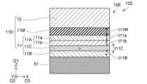
- FIG. 5 is a schematic cross-sectional view illustrating the magnetic device according to the first embodiment. 5, in the magnetic device 102 according to the embodiment, the first magnetic region 11A includes a plurality of portions. Except for this, the configuration of the magnetic device 102 may be similar to the configuration of the magnetic device 101.
- the first magnetic region 11A includes a first magnetic portion 11a and a second magnetic portion 11b.
- the second magnetic portion 11b is provided between the first intermediate region 11C and the first magnetic portion 11a.
- the first magnetic portion 11a includes Co, Fe, and B.
- the second magnetic portion 11b includes Co.
- the second magnetic portion 11b does not include Fe.
- the concentration of Fe in the second magnetic portion 11b is lower than the concentration of Fe in the first magnetic portion 11a. This configuration enables more stable switching of magnetization.
- the thickness of the first magnetic portion 11a in the first direction D1 is the first magnetic portion thickness t11a.
- the first magnetic portion thickness t11a is 0.3 nm or more and 4 nm or less.
- the thickness of the second magnetic portion 11b in the first direction D1 is the second magnetic portion thickness t11b.
- the second magnetic portion thickness t11b is 0.3 nm or more and 3 nm or less.
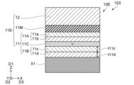
- FIG. 6 is a schematic cross-sectional view illustrating the magnetic device according to the first embodiment. 6, in the magnetic device 103 according to the embodiment, the second magnetic region 11B includes a plurality of portions. Except for this, the configuration of the magnetic device 103 may be similar to that of the magnetic device 101 or the magnetic device 102.
- the second magnetic region 11B includes a third magnetic portion 11c and a fourth magnetic portion 11d.
- the fourth magnetic portion 11d is provided between the first conductive member 51 and the third magnetic portion 11c.
- the concentration of Fe in the fourth magnetic portion 11d is higher than the concentration of Fe in the third magnetic portion 11c.
- the third magnetic portion 11c and the fourth magnetic portion 11d include Co and Fe. The concentration of Fe changes in the third magnetic portion 11c and the fourth magnetic portion 11d.
- the low concentration of Fe in the third magnetic portion 11c makes it easier to obtain, for example, a crystal lattice with a face-centered orientation. This makes it easier to obtain good lattice matching between the third magnetic portion 11c and the first intermediate region 11C containing Ir.
- the high concentration of Fe in the fourth magnetic portion 11d makes it easier to obtain, for example, a small write threshold current Iw.
- FIG. 7 is a schematic cross-sectional view illustrating the magnetic device according to the first embodiment. 7, in the magnetic device 104 according to the embodiment, the first element portion 11E includes a first intermediate layer 11D. Except for this, the configuration of the magnetic device 104 may be the same as the configuration of the magnetic device 101, the magnetic device 102, or the magnetic device 103.
- the first intermediate layer 11D is provided between the first conductive member 51 and the first magnetic layer 11.
- the first intermediate layer 11D is non-magnetic.
- the first intermediate layer 11D includes at least one selected from the group consisting of a first material, a second material, and a third material.
- the first material includes at least one selected from the group consisting of Ta, Hf, Gd, Pt, Mg, Ir, Ti, and Cu, and oxygen.
- the second material includes at least one selected from the group consisting of Ta, Hf, Gd, Pt, Mg, Ir, and Ti, and nitrogen.
- the third material includes at least one selected from the group consisting of Ta, Hf, Gd, Pt, Mg, Ir, and Ti.
- the first intermediate layer 11D including such materials enables more stable control of magnetization.
- FIG. 8 is a graph illustrating the characteristics of a magnetic device.
- Fig. 8 illustrates the calculation results of the characteristics of the magnetic device 104.
- the horizontal axis is the retention energy RE1.
- the vertical axis is the write threshold current Iw.
- Fig. 8 also illustrates the characteristics of the magnetic device 101.
- Fig. 8 illustrates the characteristics of the magnetic devices 101 and 104 when the first element portion 11E has three different sizes.
- a larger retention energy RE1 is obtained compared to the magnetic device 101.
- a smaller write threshold current Iw is obtained compared to the magnetic device 101.
- the first intermediate layer 11D is considered to function as a switching assist layer.
- the first intermediate layer 11D is considered to effectively transmit the action of spin from the first conductive member 51 to the first magnetic layer 11 without adverse effects, for example.
- the first intermediate layer 11D is considered to stabilize the magnetization of the first magnetic layer 11.
- the first conductive member 51 includes at least one selected from the group consisting of, for example, Ta, W, Pt, Hf, Re, Os, Ir, Pd, Cu, Ag, and Au.
- the first conductive member 51 may include, for example, TaB. These materials can efficiently control the magnetization of the first magnetic layer 11. For example, the effect of spin orbit torque can be effectively obtained.
- stress may be applied to the first element unit 11E.
- a configuration such as a shallow insulating member can be used to apply stress to the magnetic layer included in the first element unit 11E. This makes it easier to control the magnetization of the magnetic layer.
- the stress causes distortion in the crystal lattice of the magnetic layer. The above-mentioned effect obtained by Ir is more pronounced when combined with a configuration including the first intermediate region 11C containing Ir.
- the above configuration is applied to the first magnetic layer 11.
- the first intermediate layer 11D may be applied.
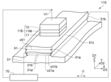
- FIG. 9 is a schematic perspective view illustrating the magnetic device according to the second embodiment.
- FIG. 10 is a schematic plan view illustrating the magnetic device according to the second embodiment.
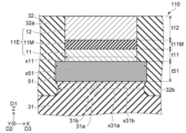
- FIG. 11 is a schematic cross-sectional view illustrating the magnetic device according to the second embodiment.
- FIG. 11 is a cross-sectional view taken along line A1-A2 of FIG.
- the magnetic device 110 according to the embodiment includes a first element portion 11E, a first conductive member 51, and a first insulating member 31.
- the first element unit 11E includes a first magnetic layer 11, a second magnetic layer 12, and a first non-magnetic layer 11M.
- a first direction D1 from the first magnetic layer 11 to the second magnetic layer 12 is defined as the Z-axis direction.
- a direction perpendicular to the Z-axis direction is defined as the Y-axis direction.
- a direction perpendicular to the Z-axis direction and the Y-axis direction is defined as the X-axis direction.
- the first non-magnetic layer 11M is provided between the first magnetic layer 11 and the second magnetic layer 12 in the first direction D1.
- the first conductive member 51 includes a first conductive portion 51a, a second conductive portion 51b, and a third conductive portion 51c.
- a second direction D2 from the first conductive portion 51a to the second conductive portion 51b intersects with the first direction D1.
- the second direction D2 is, for example, the Y-axis direction.
- the first conductive member 51 is in the form of stripes extending along the second direction D2.
- the third conductive portion 51c is provided between the first conductive portion 51a and the second conductive portion 51b in the second direction D2.
- the first magnetic layer 11 is provided between the third conductive portion 51c and the second magnetic layer 12 in the first direction D1.
- the region that overlaps with the first element portion 11E in the first direction D1 corresponds to the third conductive portion 51c.
- the third conductive portion 51c is provided between a part of the first insulating member 31 and the first element portion 11E in the first direction D1.
- the first insulating member 31 includes a first insulating portion 31a and a second insulating portion 31b.
- the first insulating portion 31a and the second insulating portion 31b overlap with the first conductive member 51 in the first direction D1.
- the second insulating portion 31b is oriented between the first insulating portion 31a and the first conductive member 51 in the first direction D1.
- the second insulating portion 31b is oriented between the first insulating portion 31a and the third conductive portion 51c in the first direction D1.
- the first insulating portion 31a is the lower portion.
- the second insulating portion 31b is provided on the first insulating portion 31a.
- the first conductive member 51 is provided on the second insulating portion 31b.
- the third direction D3 intersects with a plane including the first direction D1 and the second direction D2.
- the third direction D3 is, for example, the X-axis direction.
- the length of the first insulating portion 31a along the third direction D3 is defined as the first insulating portion width x31a.
- the length of the second insulating portion 31b along the third direction D3 is defined as the second insulating portion width x31b.
- the first insulating portion width x31a is narrower than the second insulating portion width x31b. With this configuration, stable characteristics are obtained. Stable operation is obtained.
- a control unit 70 may be provided.
- the control unit 70 may be included in the magnetic device 110.
- the control unit 70 may be provided separately from the magnetic device 110.
- the control unit 70 can supply a current i1 to the first conductive member 51.
- the current i1 has a direction from the first conductive portion 51a to the second conductive portion 51b, or a direction from the second conductive portion 51b to the first conductive portion 51a.
- the direction of the current i1 can be controlled, for example, by the control unit 70.
- the direction of magnetization of the first magnetic layer 11 can be controlled by the current i1.
- the state of change in the magnetization of the first magnetic layer 11 differs depending on the direction of the current i1.
- the electrical resistance of the first element unit 11E changes depending on the change in the angle between the magnetization of the first magnetic layer 11 and the magnetization of the second magnetic layer 12.
- the first magnetic layer 11 is a switching layer.
- the second magnetic layer 12 is, for example, a reference layer.
- the control unit 70 can apply a voltage V1 between the first conductive member 51 and the second magnetic layer 12.
- the voltage V1 changes the ease with which the magnetization of the first magnetic layer 11 changes.
- the electrical resistance of the first element unit 11E can be controlled by a combination of the voltage V1 and the current i1.
- multiple first element units 11E may be provided on one first conductive member 51.
- at least one of the multiple first element units 11E can be selected by the voltage V1, and the electrical resistance can be controlled.
- the electrical resistance between the first conductive member 51 and the second magnetic layer 12 can be changed depending on the direction of the current i1 flowing through the first conductive member 51 and the voltage V1 applied between the first conductive member 51 and the second magnetic layer 12.
- the magnetic device 110 can be used, for example, as a computing element.
- the magnetic device 110 can be used, for example, as a memory.
- the first insulating portion width x31a is narrower than the second insulating portion width x31b.
- the write current tends to be large. Conversely, when attempting to reduce the write current, the retention characteristics tend to deteriorate.
- anisotropic stress is generated due to the shape of the first insulating member 31.
- the length of the first insulating portion 31a along the second direction D2 is the first insulating portion length y31a.
- the first insulating portion length y31a is longer than the first insulating portion width x31a (see FIG. 11).
- the first insulating portion length y31a is, for example, the length of the stripe. Since the first insulating portion length y31a is longer than the first insulating portion width x31a, anisotropic stress is generated. The anisotropic stress, for example, more effectively controls the magnetization of the first magnetic layer 11.
- the length of the first conductive member 51 along the third direction D3 is the first conductive member width x51.
- the first insulating portion width x31a is narrower than the first conductive member width x51. Anisotropic stress is effectively obtained.
- the first conductive member width x51 along the third direction D3 of the first conductive member 51 is shorter than the first conductive member length y51 along the second direction D2 of the first conductive member 51.
- the first conductive member 51 is in the form of stripes extending along the second direction D2.
- the first conductive member 51 includes at least one selected from the group consisting of, for example, Ta, W, Pt, Hf, Re, Os, Ir, Pd, Cu, Ag, and Au. This makes it easier to control the magnetization of the first magnetic layer 11 by the action based on the current i1 flowing through the first conductive member 51.
- the action based on the current i1 may include, for example, a spin orbit torque.
- the length of the first element portion 11E along the third direction D3 is the first element portion width x11.
- the first element portion width x11 is narrower than the first conductive member width x51. With this configuration, the magnetization of the first magnetic layer 11 becomes easier to control.
- the length of the first element portion 11E along the second direction D2 is the first element portion length y11.
- the first element portion length y11 may be shorter than the first element portion width x11.
- the magnetization of the first magnetic layer 11 becomes easier to control. It becomes easier to arrange multiple first element portions 11E at high density along the second direction D2.
- the relationship between the first element portion length y11 and the first element portion width x11 may be arbitrary.
- the magnetic device 110 may further include a second insulating member 32.
- the second insulating member 32 is omitted.
- the second insulating member 32 includes a first insulating region 32a and a second insulating region 32b.
- the first element portion 11E is provided between the first insulating region 32a and the second insulating region 32b in the third direction D3.
- the second Young's modulus of the second insulating member 32 is lower than the first Young's modulus of the first insulating member 31. This makes it easier for the anisotropic stress caused by the first insulating member 31 to be applied more effectively to the first element portion 11E.
- the first insulating member 31 may include, for example, at least one selected from the group consisting of silicon oxide, silicon nitride, silicon oxynitride, and aluminum oxide.
- the second insulating member 32 may include a film based on TEOS (tetra ethoxy silane), a SOG (spin on glass) film, or a resin.
- the first insulating member 31 includes a first element and a second element.
- the first element includes at least one element selected from the group consisting of silicon and aluminum.
- the second element includes at least one element selected from the group consisting of oxygen and nitrogen.
- the second insulating member 32 includes silicon, oxygen, and carbon.
- the second insulating member 32 may include a resin.
- the first conductive member thickness t51 (see FIG. 11) along the first direction D1 of the first conductive member 51 is preferably, for example, 2 nm or more and 15 nm or less.
- the first magnetic layer thickness t11 (see FIG. 11) along the first direction D1 of the first magnetic layer 11 is preferably, for example, 0.7 nm or more and 5 nm or less.
- the first non-magnetic layer thickness t11M (see FIG. 11) along the first direction D1 of the first non-magnetic layer 11M is preferably, for example, 0.8 nm or more and 2 nm or less.
- the second magnetic layer thickness t12 (see FIG. 11) along the first direction D1 of the second magnetic layer 12 is preferably, for example, 1 nm or more and 6 nm or less.
- the first nonmagnetic layer 11M includes, for example, at least one selected from the group consisting of MgO, CaO, SrO, TiO, VO, NbO, and Al 2 O 3.
- the first element unit 11E is, for example, a TMR (Tunnel Magneto Resistance) element.
- the first magnetic layer 11 preferably contains, for example, Co x Fe 1-x B.
- the composition ratio x is preferably 0.1 or more and 0.6 or less.
- good element characteristics are easily obtained.
- large resistance change is easily obtained.
- highly stable magnetization is easily obtained.
- a small write current is easily obtained.
- these characteristics are easily obtained simultaneously.
- the concentration of B (boron) in Co x Fe 1-x B is preferably, for example, 5 atm % or more and 30 atm % or less.
- the second magnetic layer 12 may include multiple laminated films.
- FIG. 12 is a schematic cross-sectional view illustrating the magnetic device according to the second embodiment. 12, in the magnetic device 111 according to the embodiment, the second magnetic layer 12 includes a plurality of magnetic films 12m and a plurality of non-magnetic films 12n. Except for this, the configuration of the magnetic device 111 may be similar to that of the magnetic device 110.
- one of the multiple magnetic films 12m is between one of the multiple non-magnetic films 12n and another of the multiple non-magnetic films 12n.
- one of the multiple non-magnetic films 12n is between one of the multiple magnetic films 12m and another of the multiple magnetic films 12m.
- the second magnetic layer 12 has, for example, a SAF (synthetic anti-ferromagnetic) structure. More stable magnetic properties are easily obtained in the second magnetic layer 12.
- the non-magnetic films 12n each include, for example, at least one selected from the group consisting of Ru and Ir.
- the non-magnetic film thickness t12n of one of the non-magnetic films 12n along the first direction D1 is preferably, for example, 0.2 nm or more and 2.0 nm or less.
- the multiple magnetic films 12m include, for example, at least one selected from the group consisting of Fe and Co.
- the magnetic film thickness t12m along the first direction D1 of one of the multiple magnetic films 12m is preferably, for example, 0.2 nm or more and 5.0 nm or less.
- the magnetic device 111 may include a conductive layer 26.
- the second magnetic layer 12 is between the first non-magnetic layer 11M and the conductive layer 26.
- the conductive layer 26 includes, for example, at least one selected from the group consisting of Cu, Al, and Au.
- the conductive layer 26 is, for example, an electrode.
- the magnetic device 111 may include an intermediate conductive layer 25.
- the intermediate conductive layer 25 is between the second magnetic layer 12 and the conductive layer 26.
- the intermediate conductive layer 25 includes at least one selected from the group consisting of Ti and Ta, for example.
- the intermediate conductive layer 25 is, for example, along the cap. This makes it easier to obtain a stable second magnetic layer 12.
- FIG. 13 is a micrograph image illustrating the magnetic device according to the second embodiment.
- FIG. 13 is a high-angle annular dark field scanning transmission electron microscopy (HAADF-STEM) image of the magnetic device 111.
- the first insulating member 31 includes a first insulating portion 31a and a second insulating portion 31b.
- the width of the first insulating portion 31a along the X-axis direction (x31a: see FIG. 11) is narrower than the width of the second insulating portion 31b along the X-axis direction (x31b: see FIG. 11).
- the width of the first insulating portion 31a along the X-axis direction is narrower than the width of the first conductive member 51 along the X-axis direction (x51: see FIG. 11). Such a configuration is obtained by over-etching the first insulating member 31 in processing the first insulating member 31.
- the width of the first element portion 11E along the X-axis direction may be narrower than the width of the first conductive member 51 along the X-axis direction.
- the first conductive member 51 may be curved in a convex shape from the first insulating portion 31a toward the first element portion 11E.
- the first conductive member 51 may be deformed in response to stress.
- the retention characteristic is 150 k B T or more. This value corresponds to non-volatility for 10 years or more.
- the write current threshold in the first sample is less than 50 ⁇ A.
- the width (x31a) of the first insulating portion 31a along the X-axis direction is the same as the width (x51) of the first conductive member 51 along the X-axis direction.
- the retention characteristic is about 50 k B T to 80 k B T.
- the write current threshold in the second sample exceeds 50 ⁇ A, for example, 50 ⁇ A to 75 ⁇ A. In this way, in the magnetic device according to the embodiment (such as the magnetic device 111), good retention characteristics and a small write current are obtained.
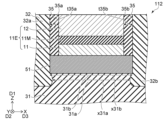
- FIG. 14 is a schematic cross-sectional view illustrating the magnetic device according to the second embodiment. 14, the magnetic device 112 according to the embodiment further includes an intermediate insulating member 35. Except for this, the configuration of the magnetic device 112 may be similar to the configuration of the magnetic device 110 or the magnetic device 111.
- the intermediate insulating member 35 includes a first intermediate insulating portion 35a and a second intermediate insulating portion 35b.
- the first intermediate insulating portion 35a is provided between the first insulating region 32a and the first element portion 11E in the third direction D3.
- the second intermediate insulating portion 35b is provided between the first element portion 11E and the second insulating region 32b in the third direction D3.
- the Young's modulus of the intermediate insulating member 35 is higher than the second Young's modulus.
- the intermediate insulating member 35 may, for example, contain at least one selected from the group consisting of silicon oxide, silicon nitride, silicon oxynitride, and aluminum oxide.
- the intermediate insulating member 35 may, for example, contain at least one selected from the group consisting of silicon and aluminum, and at least one selected from the group consisting of oxygen and nitrogen.
- the second insulating member 32 contains silicon, oxygen, and carbon.
- the second insulating member 32 may contain a resin.
- the intermediate insulating member 35 functions, for example, as a passivation film. A stable first element portion 11E is easily obtained.
- the first intermediate insulating portion thickness t35a along the third direction D3 of the first intermediate insulating portion 35a is preferably, for example, 1 nm or more and 5 nm or less.
- the second intermediate insulating portion thickness t35b along the third direction D3 of the second intermediate insulating portion 35b is preferably, for example, 1 nm or more and 5 nm or less. Good protective characteristics are obtained.
- the stress based on the first insulating member 31 is applied to the first element portion 11E without being impaired.
- FIG. 15 is a schematic cross-sectional view illustrating the magnetic device according to the second embodiment. 15, the magnetic device 113 according to the embodiment further includes a third insulating member 33.
- the configuration of the magnetic device 113 other than this may be similar to the configuration of the magnetic device 110, the magnetic device 111 or the magnetic device 112.
- the first element portion 11E is provided between the third conductive portion 51c and at least a part of the third insulating member 33 in the first direction D1.
- the third Young's modulus of the third insulating member 33 is lower than the first Young's modulus of the first insulating member 31.
- the third insulating member 33 may include a TEOS-based film, an SOG film, a resin, or the like.
- a first conductive layer 61 may be provided.
- the first conductive layer 61 is, for example, a wiring.
- a third insulating member 33 with a low Young's modulus is provided between the first element portion 11E and the first conductive layer 61. By providing the third insulating member 33 with a low Young's modulus, stress caused by the first conductive layer 61 is less likely to be applied to the first element portion 11E. The desired anisotropic stress is effectively applied to the first magnetic layer 11. Even when the first conductive layer 61 is provided, stable characteristics can be maintained. Stable operation can be obtained.
- FIG. 16 is a schematic cross-sectional view illustrating the magnetic device according to the second embodiment. 16, the magnetic device 114 according to the embodiment further includes a fourth insulating member 34. Except for this, the configuration of the magnetic device 114 may be similar to the configuration of the magnetic device 113.
- the first insulating portion 31a is provided between at least a portion of the fourth insulating member 34 and the first conductive member 51 in the first direction D1.
- the fourth Young's modulus of the fourth insulating member 34 is lower than the first Young's modulus of the first insulating member 31.
- the fourth insulating member 34 may include a TEOS-based film, an SOG film, a resin, or the like.
- a second conductive layer 62 may be provided.
- the second conductive layer 62 may be, for example, a wiring.
- the fourth insulating member 34 is provided between the second conductive layer 62 and the first insulating member 31. By providing the fourth insulating member 34 with a low Young's modulus, the stress caused by the second conductive layer 62 is alleviated.
- FIG. 17 is a schematic cross-sectional view illustrating the magnetic device according to the third embodiment.
- the magnetic device 120 also includes a first element unit 11E, a first conductive member 51, and a first insulating member 31.
- the first element unit 11E also includes a first magnetic layer 11, a second magnetic layer 12, and a first nonmagnetic layer (see FIG. 9).
- the first conductive member 51 includes a first conductive portion 51a, a second conductive portion 51b, and a third conductive portion 51c.
- the first insulating member 31 includes a first insulating portion 31a.
- the third conductive portion 51c is provided between a part of the first insulating portion 31a and the first element unit 11E in the first direction D1.
- the configurations of the first element unit 11E and the first conductive member 51 may be the same as those in the magnetic device 110 or the magnetic device 111.
- a third conductive portion 51c is provided between the first insulating portion 31a and the first magnetic layer 11 in the first direction D1.
- the first insulating portion width x31a along the third direction D3 of the first insulating portion 31a is narrower than the first conductive member width x51 along the third direction D3 of the first conductive member 51.
- the third direction D3 intersects with a plane including the first direction D1 and the second direction D2.
- the write current can be reduced. Stable characteristics are obtained. Stable operation is obtained.
- the first element portion width x11 along the third direction D3 of the first element portion 11E may be narrower than the first conductive member width x51 (see FIG. 10).
- the magnetic device 120 may further include a second insulating member 32.
- the second insulating member 32 includes a first insulating region 32a and a second insulating region 32b.
- the first element portion 11E is provided between the first insulating region 32a and the second insulating region 32b in the third direction D3.
- the second Young's modulus of the second insulating member 32 is lower than the first Young's modulus of the first insulating member 31.
- the materials of the second insulating member 32 and the first insulating member 31 may be the same as those described in relation to the second embodiment.
- the magnetic device 120 may further include an intermediate insulating member 35.
- the intermediate insulating member 35 may include a first intermediate insulating portion 35a and a second intermediate insulating portion 35b.
- the first intermediate insulating portion 35a is provided between the first insulating region 32a and the first element portion 11E in the third direction D3.
- the second intermediate insulating portion 35b is provided between the first element portion 11E and the second insulating region 32b in the third direction D3.
- the Young's modulus of the intermediate insulating member 35 is higher than the second Young's modulus.
- the material of the intermediate insulating member 35 may be the same as the material of the intermediate insulating member 35 described in relation to the second embodiment.
- the magnetic device 120 may further include a third insulating member 33 (see FIG. 15).
- the first element portion 11E is disposed between the third conductive portion 51c and at least a portion of the third insulating member 33 in the first direction D1.
- the third Young's modulus of the third insulating member 33 is lower than the first Young's modulus of the first insulating member 31.
- the material of the third insulating member 33 may be the same as the material of the third insulating member 33 described in relation to the second embodiment.
- the magnetic device 120 may further include a fourth insulating member 34 (see FIG. 16).
- the first insulating portion 31a is provided between at least a portion of the fourth insulating member 34 and the first conductive member 51 in the first direction D1.
- the fourth Young's modulus of the fourth insulating member 34 is lower than the first Young's modulus of the first insulating member 31.
- the first magnetic layer 11 may contain Co x Fe 1-x B, where the composition ratio x is equal to or greater than 0.1 and equal to or less than 0.6.
- FIG. 18 is a schematic cross-sectional view illustrating the magnetic device according to the fourth embodiment.
- the magnetic device 130 according to the embodiment includes a first element portion 11E, a first conductive member 51, a first insulating member 31, and a third insulating member 33.
- the configurations of the first element portion 11E and the first conductive member 51 in the magnetic device 130 may be similar to those in the magnetic device 110 and the like.
- the first conductive member 51 also includes a first conductive portion 51a, a second conductive portion 51b, and a third conductive portion 51c.
- the first insulating member 31 includes a first insulating portion 31a.
- the third conductive portion 51c is provided between the first insulating portion 31a and the first element portion 11E in the first direction D1.
- the length of the first insulating portion 31a along the second direction D2 is longer than the length of the first insulating portion 31a along the third direction D3 (first insulating portion width x31a) (see FIG. 11).
- the first insulating portion 31a is, for example, a stripe.
- the first insulating portion 31a is striped and extends along the second direction D2.
- Anisotropic stress is generated due to the anisotropic planar shape of the first insulating portion 31a. The anisotropic stress, for example, more effectively controls the magnetization of the first magnetic layer 11.
- the third conductive portion 51c is provided between a part of the first insulating member 31 and the first element portion 11E in the first direction D1.
- the first element portion 11E is provided between the third conductive portion 51c and at least a part of the third insulating member 33 in the first direction D1.
- the third Young's modulus of the third insulating member 33 is lower than the first Young's modulus of the first insulating member 31.
- the stress caused by other members is alleviated. This allows the anisotropic stress from the first insulating member 31 to be effectively applied to the first magnetic layer 11. Good retention characteristics can also be obtained in the magnetic device 130. The write current can be reduced. Stable characteristics can be obtained. Stable operation can be obtained.
- FIG. 19 is a schematic cross-sectional view illustrating the magnetic device according to the fourth embodiment.
- a magnetic device 131 according to the embodiment includes a first element portion 11E, a first conductive member 51, a first insulating member 31, and a third insulating member 33.
- the position of the third insulating member 33 is different from the position of the third insulating member 33 in the magnetic device 130.
- the configuration of the magnetic device 131 may be similar to the configuration of the magnetic device 130.
- the first insulating member 31 is provided between at least a portion of the third insulating member 33 and the first conductive member 51 in the first direction D1.
- the third Young's modulus of the third insulating member 33 is lower than the first Young's modulus of the first insulating member 31.
- the first insulating member 31 may include, for example, at least one selected from the group consisting of silicon oxide, silicon nitride, silicon oxynitride, and aluminum oxide.
- the third insulating member 33 may include a TEOS-based film, a SOG (Spin On Glass) film, or a resin, etc.
- the first insulating member 31 includes a first element and a second element.
- the first element includes at least one element selected from the group consisting of silicon and aluminum.
- the second element includes at least one element selected from the group consisting of oxygen and nitrogen.
- the third insulating member 33 includes silicon, oxygen, and carbon.
- the third insulating member 33 may include a resin.
- a second insulating member 32 may be provided in the magnetic device 130 and the magnetic device 131.
- An intermediate insulating member 35 may be provided in the magnetic device 130 and the magnetic device 131.
- the embodiments may include the following technical solutions.
- (Technical proposal 1) A first conductive member; A first element portion; Equipped with the first element portion includes a first magnetic layer, a second magnetic layer, and a first non-magnetic layer, the first magnetic layer is provided between the first conductive member and the second magnetic layer, the first nonmagnetic layer is provided between the first magnetic layer and the second magnetic layer in a first direction from the first magnetic layer to the second magnetic layer,
- the first magnetic layer is a first magnetic region provided between the first conductive member and the first nonmagnetic layer; a second magnetic region provided between the first conductive member and the first magnetic region; a first intermediate region including Ir and provided between the second magnetic region and the first magnetic region; 2.
- a magnetic device comprising:
- the first magnetic region is A first magnetic portion; a second magnetic portion provided between the first intermediate region and the first magnetic portion; Including, the first magnetic portion includes Co, Fe, and B; The second magnetic portion includes Co, The magnetic device described in Technical Solution 1 or 2, wherein the second magnetic portion does not contain Fe, or the concentration of Fe in the second magnetic portion is lower than the concentration of Fe in the first magnetic portion.
- the second magnetic layer is A third magnetic portion; and a fourth magnetic portion provided between the first conductive member and the third magnetic portion; Including, A magnetic device described in any one of technical proposals 1 to 5, wherein the concentration of Fe in the fourth magnetic portion is higher than the concentration of Fe in the third magnetic portion.
- the first element portion further includes a non-magnetic first intermediate layer provided between the first conductive member and the first magnetic layer, the first intermediate layer includes at least one selected from the group consisting of a first material, a second material, and a third material;
- the first material includes at least one selected from the group consisting of Ta, Hf, Gd, Pt, Mg, Ir, Ti, and Cu, and oxygen;
- the second material includes at least one selected from the group consisting of Ta, Hf, Gd, Pt, Mg, Ir, and Ti, and nitrogen;
- the magnetic device according to any one of technical proposals 1 to 6, wherein the third material includes at least one selected from the group consisting of Ta, Hf, Gd, Pt, Mg, Ir and Ti.
- a first insulating member is further provided, the first conductive member includes a first conductive portion, a second conductive portion, and a third conductive portion; a second direction from the first conductive portion to the second conductive portion intersects with the first direction; the third conductive portion is provided between the first conductive portion and the second conductive portion in the second direction, the first magnetic layer is provided between the third conductive portion and the second magnetic layer in the first direction, the third conductive portion is provided between a part of the first insulating member and the first element portion in the first direction, the first insulating member includes a first insulating portion and a second insulating portion, the second insulating portion is provided between the first insulating portion and the first conductive member in the first direction, a first insulating portion width along the third direction of the first insulating portion is narrower than a second insulating portion width along the third direction of the second insulating portion; A magnetic device described in any one of technical proposals 1 to 8, wherein the third direction intersects with
- the first magnetic layer includes Co x Fe 1-x B; The magnetic device according to any one of technical proposals 1 to 17, wherein x is greater than or equal to 0.1 and less than or equal to 0.6.
- a first insulating member is further provided, the first conductive member includes a first conductive portion, a second conductive portion, and a third conductive portion; a second direction from the first conductive portion to the second conductive portion intersects with the first direction; the third conductive portion is provided between the first conductive portion and the second conductive portion in the second direction, the first magnetic layer is provided between the third conductive portion and the second magnetic layer in the first direction,
- the first insulating member includes a first insulating portion, the third conductive portion is provided between a part of the first insulating portion and the first element portion in the first direction, the third conductive portion is provided between the first insulating portion and the first magnetic layer in the first direction; a first insulating portion width along the third direction of the first insulating portion is narrower than a first conductive member width along the third direction of the first conductive member, A magnetic device described in any one of technical proposals 1 to 8, wherein the third direction intersects with a plane including the first direction and the second direction.
- the first magnetic layer includes Co x Fe 1-x B;
- the first conductive member includes a first conductive portion, a second conductive portion, and a third conductive portion; a second direction from the first conductive portion to the second conductive portion intersects with the first direction; the third conductive portion is provided between the first conductive portion and the second conductive portion in the second direction, the first magnetic layer is provided between the third conductive portion and the second magnetic layer in the first direction,
- the first insulating member includes a first insulating portion, the third conductive portion is provided between the first insulating portion and the first element portion in the first direction, the first element portion is provided between the third conductive portion and at least a portion of the third insulating member in the first direction, or the first insulating member is provided between at least a portion of the third insulating member and the first conductive member in the first direction,
- the present invention is not limited to these specific examples.
- the specific configurations of each element included in the magnetic device such as the element portion, magnetic layer, non-magnetic member, magnetic member, intermediate layer, intermediate member, conductive member, and insulating member, are included within the scope of the present invention as long as a person skilled in the art can implement the present invention in a similar manner and obtain similar effects by appropriately selecting from the known range.
Landscapes
- Hall/Mr Elements (AREA)
Priority Applications (3)
| Application Number | Priority Date | Filing Date | Title |
|---|---|---|---|
| PCT/JP2023/029712 WO2025037420A1 (ja) | 2023-08-17 | 2023-08-17 | 磁気デバイス |
| CN202380100935.4A CN121621042A (zh) | 2023-08-17 | 2023-08-17 | 磁器件 |
| JP2025540588A JPWO2025037420A1 (https=) | 2023-08-17 | 2023-08-17 |
Applications Claiming Priority (1)
| Application Number | Priority Date | Filing Date | Title |
|---|---|---|---|
| PCT/JP2023/029712 WO2025037420A1 (ja) | 2023-08-17 | 2023-08-17 | 磁気デバイス |
Publications (1)
| Publication Number | Publication Date |
|---|---|
| WO2025037420A1 true WO2025037420A1 (ja) | 2025-02-20 |
Family
ID=94632858
Family Applications (1)
| Application Number | Title | Priority Date | Filing Date |
|---|---|---|---|
| PCT/JP2023/029712 Pending WO2025037420A1 (ja) | 2023-08-17 | 2023-08-17 | 磁気デバイス |
Country Status (3)
| Country | Link |
|---|---|
| JP (1) | JPWO2025037420A1 (https=) |
| CN (1) | CN121621042A (https=) |
| WO (1) | WO2025037420A1 (https=) |
Citations (4)
| Publication number | Priority date | Publication date | Assignee | Title |
|---|---|---|---|---|
| JP2018098432A (ja) * | 2016-12-16 | 2018-06-21 | 株式会社東芝 | 磁気記憶装置 |
| WO2019138778A1 (ja) * | 2018-01-10 | 2019-07-18 | 国立大学法人東北大学 | 磁気抵抗効果素子及び磁気メモリ |
| WO2020166141A1 (ja) * | 2019-02-13 | 2020-08-20 | 国立大学法人東北大学 | 磁性積層膜、磁気メモリ素子及び磁気メモリ |
| WO2021149242A1 (ja) * | 2020-01-24 | 2021-07-29 | Tdk株式会社 | スピン素子及びリザボア素子 |
-
2023
- 2023-08-17 CN CN202380100935.4A patent/CN121621042A/zh active Pending
- 2023-08-17 JP JP2025540588A patent/JPWO2025037420A1/ja active Pending
- 2023-08-17 WO PCT/JP2023/029712 patent/WO2025037420A1/ja active Pending
Patent Citations (4)
| Publication number | Priority date | Publication date | Assignee | Title |
|---|---|---|---|---|
| JP2018098432A (ja) * | 2016-12-16 | 2018-06-21 | 株式会社東芝 | 磁気記憶装置 |
| WO2019138778A1 (ja) * | 2018-01-10 | 2019-07-18 | 国立大学法人東北大学 | 磁気抵抗効果素子及び磁気メモリ |
| WO2020166141A1 (ja) * | 2019-02-13 | 2020-08-20 | 国立大学法人東北大学 | 磁性積層膜、磁気メモリ素子及び磁気メモリ |
| WO2021149242A1 (ja) * | 2020-01-24 | 2021-07-29 | Tdk株式会社 | スピン素子及びリザボア素子 |
Also Published As
| Publication number | Publication date |
|---|---|
| CN121621042A (zh) | 2026-03-06 |
| JPWO2025037420A1 (https=) | 2025-02-20 |
Similar Documents
| Publication | Publication Date | Title |
|---|---|---|
| US12501838B2 (en) | Spin current magnetization rotational element, magnetoresistance effect element, and magnetic memory | |
| US12290002B2 (en) | Magnetization rotational element, magnetoresistance effect element, semiconductor element, magnetic recording array, and method for manufacturing magnetoresistance effect element | |
| US10580472B2 (en) | Magnetic memory device | |
| US10797229B2 (en) | Magnetic memory device | |
| US10096770B2 (en) | Magnetic memory device and method for manufacturing the same | |
| JP5085703B2 (ja) | 磁気記録素子および不揮発性記憶装置 | |
| KR101983856B1 (ko) | 기억 소자, 기억 장치 | |
| JP6200471B2 (ja) | 磁気メモリ | |
| US20120236633A1 (en) | Magnetic recording element and nonvolatile memory device | |
| US10170694B1 (en) | Magnetic memory | |
| CN101030443A (zh) | 磁阻效应元件和磁存储器 | |
| US10388854B2 (en) | Magnetic memory device | |
| WO2019045055A1 (ja) | スピン軌道トルク型磁化反転素子及び磁気メモリ | |
| JPWO2019230341A1 (ja) | スピン軌道トルク型磁化回転素子、スピン軌道トルク型磁気抵抗効果素子及び磁気メモリ | |
| US10276786B2 (en) | Magnetic memory | |
| JP7555200B2 (ja) | 磁気抵抗素子,磁気メモリ及び磁気抵抗素子の製造方法 | |
| WO2025037420A1 (ja) | 磁気デバイス | |
| TW202238984A (zh) | 磁儲存裝置 | |
| US20260076097A1 (en) | Magnetic device | |
| US10998490B2 (en) | Magnetic element | |
| KR102586671B1 (ko) | 자성 메모리 셀 | |
| JP2007281247A (ja) | スピンメモリ | |
| WO2019187800A1 (ja) | 磁気抵抗効果素子及び磁気メモリ | |
| US20220190234A1 (en) | Magnetization rotation element, magnetoresistance effect element, magnetic memory, and method of manufacturing spin-orbit torque wiring | |
| US12598918B2 (en) | Magneto-resistive element and method of manufacturing the magneto-resistive element |
Legal Events
| Date | Code | Title | Description |
|---|---|---|---|
| 121 | Ep: the epo has been informed by wipo that ep was designated in this application |
Ref document number: 23949188 Country of ref document: EP Kind code of ref document: A1 |
|
| ENP | Entry into the national phase |
Ref document number: 2025540588 Country of ref document: JP Kind code of ref document: A |
|
| WWE | Wipo information: entry into national phase |
Ref document number: 2025540588 Country of ref document: JP |
|
| NENP | Non-entry into the national phase |
Ref country code: DE |