WO2025033118A1 - 半導体装置および電力変換装置 - Google Patents
半導体装置および電力変換装置 Download PDFInfo
- Publication number
- WO2025033118A1 WO2025033118A1 PCT/JP2024/025493 JP2024025493W WO2025033118A1 WO 2025033118 A1 WO2025033118 A1 WO 2025033118A1 JP 2024025493 W JP2024025493 W JP 2024025493W WO 2025033118 A1 WO2025033118 A1 WO 2025033118A1
- Authority
- WO
- WIPO (PCT)
- Prior art keywords
- semiconductor element
- wiring
- semiconductor
- terminal
- snubber circuit
- Prior art date
- Legal status (The legal status is an assumption and is not a legal conclusion. Google has not performed a legal analysis and makes no representation as to the accuracy of the status listed.)
- Pending
Links
Images


Classifications
-
- H—ELECTRICITY
- H02—GENERATION; CONVERSION OR DISTRIBUTION OF ELECTRIC POWER
- H02M—APPARATUS FOR CONVERSION BETWEEN AC AND AC, BETWEEN AC AND DC, OR BETWEEN DC AND DC, AND FOR USE WITH MAINS OR SIMILAR POWER SUPPLY SYSTEMS; CONVERSION OF DC OR AC INPUT POWER INTO SURGE OUTPUT POWER; CONTROL OR REGULATION THEREOF
- H02M7/00—Conversion of AC power input into DC power output; Conversion of DC power input into AC power output
- H02M7/42—Conversion of DC power input into AC power output without possibility of reversal
- H02M7/44—Conversion of DC power input into AC power output without possibility of reversal by static converters
- H02M7/48—Conversion of DC power input into AC power output without possibility of reversal by static converters using discharge tubes with control electrode or semiconductor devices with control electrode
-
- H—ELECTRICITY
- H10—SEMICONDUCTOR DEVICES; ELECTRIC SOLID-STATE DEVICES NOT OTHERWISE PROVIDED FOR
- H10W—GENERIC PACKAGES, INTERCONNECTIONS, CONNECTORS OR OTHER CONSTRUCTIONAL DETAILS OF DEVICES COVERED BY CLASS H10
- H10W90/00—Package configurations
Definitions
- the disclosure in this specification relates to semiconductor devices and power conversion devices.
- Patent Document 1 referring to Figures 1 to 3, discloses a module in which snubber circuits are adjacent to both the semiconductor element constituting the upper arm and the semiconductor element constituting the lower arm.
- the snubber circuit is arranged alongside both semiconductor elements in a direction perpendicular to the direction in which the semiconductor elements of the upper arm and the semiconductor elements of the lower arm are arranged.
- the snubber circuit faces both semiconductor elements, so it is susceptible to the effects of heat dissipation from both semiconductor elements.
- the purpose of the disclosure in this specification is to provide a semiconductor device and a power conversion device that aim to reduce the thermal effect of semiconductor elements on snubber circuits.
- One of the disclosed semiconductor devices includes a first semiconductor element forming an upper arm, a second semiconductor element arranged in parallel with the first semiconductor element and forming a lower arm, and snubber circuit components forming a snubber circuit connected in parallel with the upper arm and the lower arm,
- the snubber circuit component is provided adjacent to a semiconductor element group in which the first semiconductor element and the second semiconductor element are formed side by side in an element arrangement direction in which the first semiconductor element and the second semiconductor element are arranged.
- one of the disclosed power conversion devices includes the above-mentioned semiconductor device and a smoothing capacitor.
- This semiconductor device provides a snubber circuit component that is adjacent to one of the first and second semiconductor elements arranged side by side but not adjacent to the other. This makes it possible to suppress the thermal effect of the other of the semiconductor elements constituting the upper and lower arms on the snubber circuit. This semiconductor device can suppress the thermal effect of the semiconductor elements on the snubber circuit. Furthermore, a configuration including this semiconductor device can provide a power conversion device that can suppress the thermal effect of the semiconductor elements on the snubber circuit.
- FIG. 1 is a circuit diagram of a power conversion device according to a first embodiment.
- FIG. 1 is a plan view illustrating a configuration of a semiconductor device. 1 is a cross-sectional view showing a configuration of a portion of a semiconductor device; 4 is a plan view showing the positional relationship between the semiconductor elements and snubber circuits of the upper and lower arms.
- FIG. 4 is a plan view showing the positional relationship between the semiconductor elements and snubber circuits of the upper and lower arms.
- FIG. 4 is a plan view showing the positional relationship between the semiconductor elements and snubber circuits of the upper and lower arms.
- FIG. 4 is a plan view showing the positional relationship between the semiconductor elements and snubber circuits of the upper and lower arms.
- the power conversion device can be applied to an on-board power conversion device mounted on vehicles such as electric cars, hybrid cars, and plug-in hybrid cars.
- the power conversion device can also be mounted on flying objects such as electric vertical take-off and landing aircraft and drones, ships, construction machinery, agricultural machinery, and the like.
- flying objects such as electric vertical take-off and landing aircraft and drones, ships, construction machinery, agricultural machinery, and the like.
- the vehicle drive system 1 includes a DC power source 2, a motor generator 3, and a power conversion device 4.
- the DC power source 2 is a DC voltage source composed of a chargeable and dischargeable secondary battery.
- the secondary battery is, for example, a lithium ion battery, a nickel-metal hydride battery, etc.
- the motor generator 3 is, for example, a three-phase AC rotating electric machine.
- the motor generator 3 functions as a drive source for the vehicle, i.e., an electric motor.
- the motor generator 3 functions as a generator during regeneration.
- the power conversion device 4 performs power conversion between the DC power source 2 and the motor generator 3.
- the power conversion device 4 includes a power conversion circuit. As shown in FIG. 1, the power conversion device 4 includes a smoothing capacitor 5 and an inverter 6, which is a power conversion circuit.
- the smoothing capacitor 5 mainly functions to smooth the DC voltage supplied from the DC power source 2.
- the smoothing capacitor 5 is connected to a P line 7, which is a power supply line on the high potential side, and an N line 8, which is a power supply line on the low potential side.
- the smoothing capacitor 5 is connected in parallel to the DC power supply 2.
- the P line 7 is connected to the positive terminal of the DC power supply 2.
- the N line 8 is connected to the negative terminal of the DC power supply 2.
- the positive terminal of the smoothing capacitor 5 is connected to the P line 7 between the DC power supply 2 and the inverter 6.
- the negative terminal of the smoothing capacitor 5 is connected to the N line 8 between the DC power supply 2 and the inverter 6.
- the P line 7 has a plurality of P bus bars that connect electrical components to each other.
- the N line 8 has a plurality of N bus bars that connect electrical components to each other.
- the inverter 6 is a DC-AC conversion circuit. In accordance with switching control by a control circuit provided on the control circuit board, the inverter 6 converts DC voltage into three-phase AC voltage and outputs it to the motor generator 3. This operation drives the motor generator 3 to generate a predetermined torque. During regenerative braking of the vehicle, the inverter 6 converts the three-phase AC voltage generated by the motor generator 3 in response to rotational force from the wheels into DC voltage in accordance with switching control of the control circuit. The converted DC power is output to the P line 7. In this way, the inverter 6 performs bidirectional power conversion between the DC power source 2 and the motor generator 3.
- the control circuit for the switching element generates a drive command for operating the MOSFET 11 and outputs it to the drive circuit.
- the control circuit generates the drive command based on, for example, a torque request input from a higher-level ECU and signals detected by various sensors.
- ECU is an abbreviation for Electronic Control Unit.
- the various sensors include, for example, a current sensor, a rotation angle sensor, and a voltage sensor.
- the current sensor detects the phase current flowing through the winding 3a of each phase.
- the rotation angle sensor detects the rotation angle of the rotor of the motor generator 3.
- the voltage sensor detects the voltage across the smoothing capacitor 5.
- the control circuit outputs, for example, a PWM signal as the drive command.
- the control circuit is configured to include, for example, a processor and a memory.
- PWM is an abbreviation for Pulse Width Modulation.
- the inverter 6 has upper and lower arm circuits 9 corresponding to each of the three phases.
- the upper and lower arm circuits 9 are sometimes referred to as legs.
- the upper and lower arm circuits 9 have an upper arm 9H and a lower arm 9L.
- the upper arm 9H and the lower arm 9L are connected in series between the P line 7 and the N line 8, with the upper arm 9H on the P line 7 side and the lower arm 9L on the N line 8 side.
- connection point between the upper arm 9H and the lower arm 9L is connected to the winding 3a of the corresponding phase in the motor generator 3 via an output line 10.
- the U-phase upper and lower arm circuit 9U is connected to the U-phase winding 3a via a corresponding output line 10.
- the V-phase upper and lower arm circuit 9V is connected to the V-phase winding 3a via a corresponding output line 10.
- the W-phase upper and lower arm circuit 9W is connected to the W-phase winding 3a via a corresponding output line 10.
- At least a portion of the output line 10 is composed of a conductive member such as a bus bar.
- Inverter 6 has six arms. Each arm has a switching element. There is no particular limit to the number of switching elements constituting each arm. There may be one or more. When there are more than one, the multiple switching elements connected in parallel are turned on and off at the same timing by a common gate drive signal.
- MOSFET is used as the switching element constituting each arm.
- MOSFET is an abbreviation for Metal Oxide Semiconductor Field Effect Transistor.
- the drain of the MOSFET 11 is connected to the P line 7.
- the source of the MOSFET 11 is connected to the N line 8.
- the source of the MOSFET 11 in the upper arm 9H and the drain of the MOSFET 11 in the lower arm 9L are connected to each other.
- a freewheeling diode 12 is connected in inverse parallel to each MOSFET 11.
- the diode 12 may be a parasitic diode of the MOSFET 11, or may be provided separately from the parasitic diode.
- the anode of the diode 12 is connected to the source of the corresponding MOSFET 11.
- the cathode of the diode 12 is connected to the drain.
- the switching element is not limited to a MOSFET 11.
- An IGBT may be used as the switching element.
- IGBT is an abbreviation for Insulated Gate Bipolar Transistor.
- a freewheeling diode is also connected in inverse parallel.
- the inverter 6 is equipped with snubber circuits 13.
- the snubber circuits 13 absorb the transient high voltage that occurs during switching, known as switching surges. This enables high-speed switching.
- the snubber circuits 13 may be provided individually for the upper and lower arm circuits 9 and connected in parallel to the corresponding upper and lower arm circuits 9.
- the snubber circuit 13 has at least a capacitor 131.
- the snubber circuit 13 may be, for example, a C snubber circuit having a capacitor 131, or an RC snubber circuit having a capacitor 131 and a resistor 132 as shown in FIG. 1. It may also be an RCD snubber circuit having a capacitor 131, a resistor 132, and a diode.
- FIG. 2 is a plan view showing the configuration of an example semiconductor device.
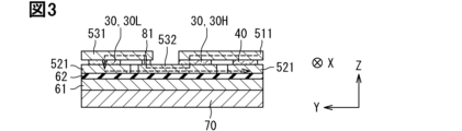
- FIG. 3 is a cross-sectional view of a portion of the semiconductor device.
- the thickness direction of the substrate is defined as the Z direction
- one direction perpendicular to the Z direction is defined as the Y direction.
- the direction perpendicular to both the Z direction and the Y direction is defined as the X direction.
- a shape viewed in a plane along the Z direction in other words a shape along the XY plane defined by the X and Y directions, is defined as a planar shape.
- a planar view in a direction along the Z direction may also be referred to simply as a planar view.
- the semiconductor device 21 includes upper and lower arm circuits 9, snubber circuit components 40, and a housing 60. As shown in FIG. 3, the semiconductor device 21 may include a cooler 70.
- the semiconductor device 21, together with other elements such as the capacitor device, may be housed in a case that forms the outer casing of the power conversion device 4.
- the semiconductor device 21 includes a first semiconductor element 30H forming the upper arm 9H and a second semiconductor element 30L forming the lower arm 9L.
- the first semiconductor element 30H and the second semiconductor element 30L form a semiconductor element group arranged side by side in the element arrangement direction.
- the element arrangement direction corresponds to the Y direction in each drawing.
- the semiconductor device 21 includes a snubber circuit component 40 arranged adjacent to the semiconductor element group in the element arrangement direction.
- the snubber circuit component 40 includes a snubber circuit 13 connected in parallel to the upper arm 9H and the lower arm 9L.
- the snubber circuit component 40 is formed, for example, from a thin-film element.
- the first semiconductor element 30H forms a flat outer shell and includes multiple semiconductor elements 30 contained inside the shell.
- the second semiconductor element 30L forms a flat outer shell and includes multiple semiconductor elements 30 contained inside the shell.
- Multiple here means two or more. There is no particular limit to the number of semiconductor elements 30 included in each of the first semiconductor element 30H and the second semiconductor element 30L. There may be one each, or multiple each.
- the multiple semiconductor elements 30 are connected in parallel to provide the MOSFET 11 of one phase arm.
- the multiple semiconductor elements 30 are lined up in the X direction.
- the flat outer shell is, for example, a thin plate or a thin film.
- Each semiconductor element 30 is arranged in such a manner that the thickness direction, which is the minimum length direction, is perpendicular to the element arrangement direction.
- the thickness direction is the plate thickness direction of the thin plate, and corresponds to the Z direction.
- the multiple semiconductor elements 30 included in the first semiconductor element 30H are arranged in a direction in which the flat maximum surface is perpendicular to both the element arrangement direction and the thickness direction.
- the multiple semiconductor elements 30 included in the second semiconductor element 30L are arranged in a direction in which the flat maximum surface is perpendicular to both the element arrangement direction and the thickness direction. As shown in FIG. 2, the multiple semiconductor elements are arranged in the X direction.
- the semiconductor element 30 is formed by forming a vertical element on a semiconductor substrate made of materials such as silicon (Si) or a wide band gap semiconductor with a wider band gap than silicon.
- Examples of wide band gap semiconductors include silicon carbide (SiC), gallium nitride (GaN), gallium oxide (Ga2O3), and diamond.
- the semiconductor element 30 is sometimes called a power element, a semiconductor chip, etc.
- the vertical element is configured to pass a main current in the thickness direction of the semiconductor element 30.
- the semiconductor element 30 is arranged so that its thickness direction is along the Z direction.
- the semiconductor element 30 has main electrodes on both sides in the thickness direction.
- the semiconductor element 30 of this embodiment is formed by forming an n-channel MOSFET 11 as a vertical element on a semiconductor substrate made of SiC.
- the semiconductor element 30 has a drain electrode on one plate-like surface as a main electrode, and a source electrode on the other plate-like surface.
- MOSFET 11 When MOSFET 11 is turned on, a current flows between the main electrodes, that is, between the drain electrode and the source electrode. If diode 12 is a parasitic diode, the source electrode also serves as the anode electrode, and the drain electrode also serves as the cathode electrode. The drain electrode is the main electrode on the high potential side, and the source electrode is the main electrode on the low potential side.
- Semiconductor element 30 has a rectangular shape when viewed in a plane in the Z direction.
- the first semiconductor element 30H and the second semiconductor element 30L are arranged at approximately the same height in the Z direction.
- the multiple semiconductor elements 30 included in the first semiconductor element 30H are arranged in the same orientation so that the drain electrodes are on the P wiring 511 side.
- the multiple semiconductor elements 30 of the first semiconductor element 30H are arranged in the same orientation so that the source electrodes are on the opposite side to the P wiring 511.
- the multiple semiconductor elements 30 included in the second semiconductor element 30L are arranged in the same orientation so that the drain electrodes are on the O wiring 531 side.
- the multiple semiconductor elements 30 of the second semiconductor element 30L are arranged in the same orientation as the multiple semiconductor elements 30 of the first semiconductor element 30H so that the source electrodes are on the N wiring 521 side.
- the semiconductor device 21 has a P terminal 51 connected to the drain electrode of the first semiconductor element 30H via a P wiring 511.
- the semiconductor device 21 has an N terminal 52 connected to the source electrode of the second semiconductor element 30L via an N wiring 521.
- the P terminal 51 is an external connection terminal electrically connected to the P line 7.
- the P terminal 51 is electrically connected to the positive terminal of the smoothing capacitor 5.
- the N terminal 52 is an external connection terminal electrically connected to the N line 8.
- the N terminal 52 is electrically connected to the negative terminal of the smoothing capacitor 5.
- the P wiring 511 is formed from a single wiring board.
- the N wiring 521 is formed from a single wiring board.
- the P terminal 51 is an end of the P wiring 511 formed from a single wiring board.
- the P terminal 51 is shaped to protrude from the snubber circuit component 40 on the opposite side to the semiconductor element group in the element arrangement direction.
- the N terminal 52 is an end of the N wiring 521 formed from a single wiring board.
- the N terminal 52 is shaped to protrude from the snubber circuit component 40 on the opposite side to the semiconductor element group in the element arrangement direction.
- the P wiring board and the N wiring board shown in FIG. 3 are provided at positions shifted from each other in the thickness direction of the first semiconductor element, which is perpendicular to the element arrangement direction and is the direction of the minimum dimension length.
- the P wiring 511 is connected to the drain electrode of the first semiconductor element 30H.
- the P wiring 511 electrically connects the drain electrode of the first semiconductor element 30H to the P terminal 51.
- the P wiring 511 is connected to the positive electrode portion of the snubber circuit 13 included in the snubber circuit component 40.
- the P wiring 511 electrically connects the positive electrode portion of the snubber circuit 13 to the P terminal 51.
- the P wiring 511 is sometimes referred to as the positive wiring, high potential power supply wiring, etc.
- the source electrode of the second semiconductor element 30L is electrically connected to the N wiring 521.
- the N wiring 521 electrically connects the source electrode of the second semiconductor element 30L to the N terminal 52.
- the N wiring 521 is connected to the negative pole of the snubber circuit 13 included in the snubber circuit component 40.
- the N wiring 521 may be referred to as the negative pole wiring, low potential power supply wiring, etc.
- the O terminal 53 is an external connection terminal electrically connected to the output line 10.
- the O terminal 53 is electrically connected to the winding 3a of the opposing phase of the motor generator 3.
- the O terminal 53 may be referred to as an output terminal, an AC terminal, etc.
- the O wiring 531 is formed of a single wiring board.
- the O terminal 53 is an end of the O wiring 531 formed of a single wiring board.
- the O terminal 53 is shaped to protrude on the opposite side of the snubber circuit component 40 with respect to the second semiconductor element 30L in the element arrangement direction.
- the O terminal 53 protrudes on the opposite side of the P terminal 51 and the N terminal 52 in the semiconductor device 21.
- the O wiring 531 is connected to the drain electrode of the second semiconductor element 30L.
- the O wiring 531 electrically connects the source electrode of the second semiconductor element 30L and the N terminal 52.
- the O wiring 532 is formed from a single wiring board.
- the O wiring 532 is connected to the source electrode of the first semiconductor element 30H.
- the P wiring 511 and the O wiring 531 are arranged at approximately the same height in the Z direction.
- the P wiring 511 and the O wiring 531 are formed so as to overlap in the element arrangement direction.
- the N wiring 521 and the O wiring 532 are arranged at approximately the same height in the Z direction.
- the N wiring 521 and the O wiring 532 are formed so as to overlap in the element arrangement direction.
- the O wiring 532 electrically connects the source electrode of the first semiconductor element 30H and the O wiring 531.
- the O wiring 531 is sometimes referred to as an output wiring, etc.
- Height adjustment member 81 is a conductive member for offsetting the height positions of O wiring 531 and O wiring 532 in the Z direction.
- the signal terminal 54 is shaped to protrude from the second semiconductor element 30L on the opposite side to the snubber circuit component 40 in the element arrangement direction.
- the signal terminal 54 is on the same side as the O terminal 53 in the semiconductor device 21, and protrudes on the opposite side to the P terminal 51 and N terminal 52.
- the signal terminal 54 is connected to a pad of the first semiconductor element 30H via a signal wiring.
- the signal terminal 55 is shaped to protrude from the second semiconductor element 30L on the opposite side to the snubber circuit component 40 in the element arrangement direction.
- the signal terminal 55 is on the same side as the O terminal 53 in the semiconductor device 21, and protrudes on the opposite side to the P terminal 51 and N terminal 52.
- the signal terminal 55 is connected to a pad of the second semiconductor element 30L via a signal wiring.
- Each signal terminal electrically connects the semiconductor element 30 to the control circuit board.
- Each signal terminal is electrically connected to a pad of the semiconductor element 30 via a connecting member such as a bonding wire.
- the signal terminal may include at least a terminal for applying a drive voltage to the gate electrode of the semiconductor element 30.
- the signal terminal may include a terminal for detecting the source potential of the semiconductor element 30.
- the signal terminal may include a terminal for detecting the drain potential of the semiconductor element 30.
- the signal terminal may include a terminal for detecting the temperature of the semiconductor element 30.
- the snubber circuit component 40 includes at least a capacitor as an electronic component, and provides the snubber circuit 13 shown in FIG. 1.
- the snubber circuit 13 is an RC snubber circuit.
- the snubber circuit 13 includes a resistor 132 in addition to a capacitor 131.
- the semiconductor device 21 is disposed on one surface of the cooler 70 in the Z direction.
- the semiconductor device 21 is fixed to the cooler 70.
- the cooler 70 is in close contact with a heat sink 61, which is a member that promotes heat dissipation.
- An insulating member 62 is interposed between the heat sink 61 and the N wiring 521 and O wiring 532.
- the insulating member 62 is a sheet-like member, grease, gel-like substance, etc., made of an insulating material.
- the components other than the cooler 70 and heat sink 61 shown in FIG. 2 are covered by the housing 60.
- the housing 60 is formed using an electrically insulating material such as resin.
- the housing 60 may be, for example, a resin molded body.
- the housing 60 may hold some of the components of the semiconductor device 21. Some of the components of the semiconductor device 21 may be molded integrally with the housing 60 as an insert part.
- the housing 60 may be fixed to the case of the power conversion device 4 together with the cooler 70.
- the housing 60 may be formed, for example, from a gel or potting resin.
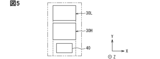
- Figures 4 to 6 show a plan view of the semiconductor device 21 in the thickness direction of the semiconductor element 30.
- the dashed lines show the extensions of the sides located at the ends in the X direction of the outer periphery of the semiconductor element group along the arrangement direction of the elements to the snubber circuit component 40.
- the snubber circuit component 40 is provided over a range including the extensions of the sides on both sides in the X direction.
- the dashed lines show the extensions of the sides located at the ends in the X direction of the outer periphery of the semiconductor element group, extending along the direction in which the elements are arranged, to the snubber circuit component 40.
- the snubber circuit component 40 is provided in an area that is inside the extensions of the sides on both sides in the X direction.
- the dashed lines show the extensions of the sides located at the ends in the X direction of the outer periphery of the semiconductor element group along the arrangement direction of the elements to the snubber circuit component 40.
- the snubber circuit component 40 is provided over an area that overlaps with one of the extensions of the sides on both sides in the X direction.
- the semiconductor device 21 includes a first semiconductor element 30H forming the upper arm 9H and a second semiconductor element 30L forming the lower arm 9L.
- the first semiconductor element 30H and the second semiconductor element 30L are arranged side by side to form a semiconductor element group.
- the semiconductor device 21 includes a snubber circuit component 40 forming a snubber circuit 13 connected in parallel to the upper arm 9H and the lower arm 9L.
- the snubber circuit component 40 is arranged adjacent to the semiconductor element group in the element arrangement direction in which the first semiconductor element 30H and the second semiconductor element 30L are arranged side by side.
- This semiconductor device 21 includes a snubber circuit component 40 that is adjacent to one of the first semiconductor element 30H and the second semiconductor element 30L that are arranged side by side but not adjacent to the other.
- This configuration realizes suppression of heat dissipation from the other of the semiconductor elements that make up the upper and lower arms to the snubber circuit 13. Therefore, the semiconductor device 21 can suppress the thermal effect of the semiconductor element group on the snubber circuit 13. Furthermore, the current flowing from the snubber circuit to the drain electrode of the first semiconductor element and the current returning from the source electrode of the second semiconductor element to the snubber circuit flow in opposite directions. Therefore, a semiconductor device that can reduce the inductance between the semiconductor elements and the snubber circuit can be provided.
- the semiconductor device 21 includes a P terminal 51 connected to the drain electrode of the first semiconductor element via a P wiring 511, and an N terminal 52 connected to the source electrode of the second semiconductor element via an N wiring 521.
- the P terminal 51 and the N terminal 52 are provided so as to protrude from the snubber circuit 13 on the opposite side to the semiconductor element group in the element arrangement direction.
- the P terminal and N terminal protrude beyond the area where the snubber circuit capacitor is mounted, so the thermal effects from the semiconductor element to both terminals can be suppressed. Furthermore, the current from the P terminal to the drain electrode of the first semiconductor element and the current from the source electrode of the second semiconductor element to the N terminal can be formed in the opposite direction. This makes it possible to provide a semiconductor device that can reduce the inductance between the semiconductor element and the smoothing capacitor 5. Furthermore, with this configuration, the device for cooling the P terminal and N terminal can be made smaller, so a power conversion device equipped with three-phase semiconductor devices can be made compact.
- the P wiring 511 extends so as to form a current from the P terminal 51 to the drain electrode of the first semiconductor element.
- the N wiring 521 extends so as to form a current from the source electrode of the second semiconductor element to the N terminal 52 in the opposite direction to the current flowing through the P wiring 511.
- At least one of the P wiring 511 and the N wiring 521 is formed from a single wiring board. With this configuration, it is possible to simplify the shape of the P wiring 511 and the N wiring 521 and to reduce the thickness of the semiconductor device. Therefore, it is possible to provide a semiconductor device that contributes to the miniaturization of the power conversion device. This configuration is useful for miniaturizing a power conversion device that includes semiconductor devices for three phases.
- Each of the P wiring 511 and the N wiring 521 is formed from a single wiring board.
- the P wiring board and the N wiring board are provided at positions offset from each other in the thickness direction of the first semiconductor element, which is perpendicular to the element arrangement direction and is the direction of the minimum dimension length.
- the semiconductor device includes an O wiring 532 that connects the source electrode of the first semiconductor element and the drain electrode of the second semiconductor element.
- the O wiring 532 and the N wiring 521 are formed to overlap in the direction in which the elements are arranged. With this configuration, it is possible to adopt a configuration that allows the P wiring, N wiring, O wiring, first semiconductor element, and second semiconductor element to be formed compactly in terms of their lengths in the thickness direction.
- the first semiconductor element 30H and the snubber circuit component 40 are arranged so as to overlap in the direction in which the elements are arranged. This configuration allows the first semiconductor element 30H and the snubber circuit component 40 to be compact in terms of their length in the thickness direction.
- the power conversion device 4 includes the semiconductor device described in this specification and a smoothing capacitor 5. As a result, as described above, it is possible to provide a power conversion device that suppresses the thermal effects of the semiconductor elements on the snubber circuit 13.
- the disclosure of this specification is not limited to the exemplified embodiments.
- the disclosure includes the exemplified embodiments and modifications by those skilled in the art based thereon.
- the disclosure is not limited to the combination of parts and elements shown in the embodiments, and can be implemented in various modifications.
- the disclosure can be implemented by various combinations.
- the disclosure can have additional parts that can be added to the embodiments.
- the disclosure includes those in which parts and elements of the embodiments are omitted.
- the disclosure includes replacement or combination of parts and elements between one embodiment and another embodiment.
- the disclosed technical scope is not limited to the description of the embodiments.
- the disclosed technical scope is indicated by the description of the claims, and should be interpreted as including all modifications within the meaning and scope equivalent to the description of the claims.
- the power conversion device 4 of the above embodiment may be further configured to include a converter as a power conversion circuit.
- the converter is a DC-DC conversion circuit that converts a DC voltage into a DC voltage of a different value. This converter is provided between the DC power source 2 and the smoothing capacitor 5.
- the converter is configured to include, for example, a reactor and the above-mentioned upper and lower arm circuits 9. In this configuration, voltage step-up and step-down are possible.
- the power conversion device 4 may be configured to include a filter capacitor that removes power supply noise from the DC power source 2. This filter capacitor is provided between the DC power source 2 and the converter.
- a power conversion device capable of achieving the objectives disclosed in the specification may be configured such that a portion of the snubber circuit overlaps a portion of the semiconductor element in the thickness direction.
- Each of the first semiconductor element and the second semiconductor element includes a plurality of semiconductor elements contained within a flat outer shell, the plurality of semiconductor elements are disposed in such a manner that a thickness direction, which is a length direction of a minimum dimension, is perpendicular to an arrangement direction of the elements,
- a semiconductor device according to technical idea 1 wherein each of the first semiconductor element and the second semiconductor element is formed by a plurality of semiconductor elements arranged in a direction perpendicular to both the element arrangement direction and the thickness direction, the largest flat surface of each of the first semiconductor element and the second semiconductor element being formed by a plurality of semiconductor elements arranged in a direction perpendicular to both the element arrangement direction and the thickness direction.
- the P wiring extends so as to form a current from the P terminal to a drain electrode of the first semiconductor element;
- the semiconductor device according to Technical Concept 3 wherein the N wiring extends so as to form a current from the source electrode of the second semiconductor element to the N terminal in a direction opposite to the direction of the current flowing through the P wiring.
- Each of the P wiring and the N wiring is formed from a single wiring board, A semiconductor device according to technical idea 5, wherein the P wiring board and the N wiring board are arranged at positions offset from each other in the thickness direction of the first semiconductor element, which is perpendicular to the arrangement direction of the elements and is the direction of the minimum dimension length.
Landscapes
- Engineering & Computer Science (AREA)
- Power Engineering (AREA)
- Inverter Devices (AREA)
Priority Applications (1)
| Application Number | Priority Date | Filing Date | Title |
|---|---|---|---|
| CN202480051281.5A CN121666685A (zh) | 2023-08-08 | 2024-07-16 | 半导体装置和电力转换装置 |
Applications Claiming Priority (2)
| Application Number | Priority Date | Filing Date | Title |
|---|---|---|---|
| JP2023129544A JP2025025085A (ja) | 2023-08-08 | 2023-08-08 | 半導体装置および電力変換装置 |
| JP2023-129544 | 2023-08-08 |
Publications (1)
| Publication Number | Publication Date |
|---|---|
| WO2025033118A1 true WO2025033118A1 (ja) | 2025-02-13 |
Family
ID=94534020
Family Applications (1)
| Application Number | Title | Priority Date | Filing Date |
|---|---|---|---|
| PCT/JP2024/025493 Pending WO2025033118A1 (ja) | 2023-08-08 | 2024-07-16 | 半導体装置および電力変換装置 |
Country Status (3)
| Country | Link |
|---|---|
| JP (1) | JP2025025085A (https=) |
| CN (1) | CN121666685A (https=) |
| WO (1) | WO2025033118A1 (https=) |
Citations (2)
| Publication number | Priority date | Publication date | Assignee | Title |
|---|---|---|---|---|
| JP2009219268A (ja) * | 2008-03-11 | 2009-09-24 | Daikin Ind Ltd | 電力変換装置 |
| JP2014053516A (ja) * | 2012-09-10 | 2014-03-20 | Hitachi Automotive Systems Ltd | パワー半導体モジュール |
-
2023
- 2023-08-08 JP JP2023129544A patent/JP2025025085A/ja active Pending
-
2024
- 2024-07-16 WO PCT/JP2024/025493 patent/WO2025033118A1/ja active Pending
- 2024-07-16 CN CN202480051281.5A patent/CN121666685A/zh active Pending
Patent Citations (2)
| Publication number | Priority date | Publication date | Assignee | Title |
|---|---|---|---|---|
| JP2009219268A (ja) * | 2008-03-11 | 2009-09-24 | Daikin Ind Ltd | 電力変換装置 |
| JP2014053516A (ja) * | 2012-09-10 | 2014-03-20 | Hitachi Automotive Systems Ltd | パワー半導体モジュール |
Also Published As
| Publication number | Publication date |
|---|---|
| CN121666685A (zh) | 2026-03-13 |
| JP2025025085A (ja) | 2025-02-21 |
Similar Documents
| Publication | Publication Date | Title |
|---|---|---|
| CN101202495B (zh) | 电力转换装置 | |
| US20240215211A1 (en) | Power conversion device | |
| JP7711821B2 (ja) | 電力変換装置 | |
| US20240213887A1 (en) | Power conversion device | |
| WO2025033118A1 (ja) | 半導体装置および電力変換装置 | |
| WO2024142671A1 (ja) | 電力変換装置 | |
| JP7392557B2 (ja) | 半導体装置 | |
| US20240145349A1 (en) | Semiconductor device | |
| US20250343105A1 (en) | Power conversion device | |
| WO2026009619A1 (ja) | 電力変換装置 | |
| WO2025173485A1 (ja) | 電力変換装置 | |
| WO2026014180A1 (ja) | 電力変換装置 | |
| WO2025182385A1 (ja) | 電力変換モジュール | |
| WO2025158813A1 (ja) | 電力変換モジュール | |
| WO2025158814A1 (ja) | 電力変換モジュール | |
| WO2025158816A1 (ja) | 電力変換モジュール | |
| JP2025113863A (ja) | 電力変換モジュール | |
| WO2026004494A1 (ja) | コンデンサモジュール | |
| WO2026009620A1 (ja) | コンデンサモジュール | |
| WO2025158815A1 (ja) | 電力変換モジュール | |
| JP2026017815A (ja) | 電力変換装置 | |
| WO2025028221A1 (ja) | 半導体モジュールおよび電力変換装置 | |
| JP2025170199A (ja) | コンデンサモジュール |
Legal Events
| Date | Code | Title | Description |
|---|---|---|---|
| 121 | Ep: the epo has been informed by wipo that ep was designated in this application |
Ref document number: 24851547 Country of ref document: EP Kind code of ref document: A1 |