WO2025032691A1 - 冷凍サイクル装置 - Google Patents
冷凍サイクル装置 Download PDFInfo
- Publication number
- WO2025032691A1 WO2025032691A1 PCT/JP2023/028777 JP2023028777W WO2025032691A1 WO 2025032691 A1 WO2025032691 A1 WO 2025032691A1 JP 2023028777 W JP2023028777 W JP 2023028777W WO 2025032691 A1 WO2025032691 A1 WO 2025032691A1
- Authority
- WO
- WIPO (PCT)
- Prior art keywords
- unit
- voltage
- conversion device
- current
- power conversion
- Prior art date
- Legal status (The legal status is an assumption and is not a legal conclusion. Google has not performed a legal analysis and makes no representation as to the accuracy of the status listed.)
- Pending
Links
Images






Classifications
-
- H—ELECTRICITY
- H02—GENERATION; CONVERSION OR DISTRIBUTION OF ELECTRIC POWER
- H02M—APPARATUS FOR CONVERSION BETWEEN AC AND AC, BETWEEN AC AND DC, OR BETWEEN DC AND DC, AND FOR USE WITH MAINS OR SIMILAR POWER SUPPLY SYSTEMS; CONVERSION OF DC OR AC INPUT POWER INTO SURGE OUTPUT POWER; CONTROL OR REGULATION THEREOF
- H02M1/00—Details of apparatus for conversion
- H02M1/12—Arrangements for reducing harmonics from AC input or output
-
- H—ELECTRICITY
- H02—GENERATION; CONVERSION OR DISTRIBUTION OF ELECTRIC POWER
- H02M—APPARATUS FOR CONVERSION BETWEEN AC AND AC, BETWEEN AC AND DC, OR BETWEEN DC AND DC, AND FOR USE WITH MAINS OR SIMILAR POWER SUPPLY SYSTEMS; CONVERSION OF DC OR AC INPUT POWER INTO SURGE OUTPUT POWER; CONTROL OR REGULATION THEREOF
- H02M7/00—Conversion of AC power input into DC power output; Conversion of DC power input into AC power output
- H02M7/42—Conversion of DC power input into AC power output without possibility of reversal
- H02M7/44—Conversion of DC power input into AC power output without possibility of reversal by static converters
- H02M7/48—Conversion of DC power input into AC power output without possibility of reversal by static converters using discharge tubes with control electrode or semiconductor devices with control electrode
Definitions
- This disclosure relates to a refrigeration cycle device equipped with a power conversion device.
- Leakage current can be a problem in refrigeration cycle equipment such as air conditioners and freezers.
- Leakage current is a high-frequency current that flows through stray capacitance between the compressor (load) and earth potential due to switching control of the switching elements equipped in the inverter.
- Leakage current that flows to earth potential returns to the refrigeration cycle equipment (source) via the ground point where the AC power supply is grounded, and is therefore also called "common mode current.”
- Patent Document 1 discloses a technology that monitors a current corresponding to a common mode current leaking from a load, and when the instantaneous value, average value or peak value of the monitored current is greater than a threshold value, controls a switch to close and outputs a compensation signal to compensate for the common mode current.
- the switch sets whether or not a detection current proportional to the monitor current is input to a compensation signal output section.
- a compensation signal is not output from the compensation signal output section unless the switch is closed.
- Patent Document 1 In air conditioners, which are one of the products to which refrigeration cycle devices are applied, an efficiency index called APF (Annual Performance Factor) is clearly stated, and the selling price is set according to the efficiency index, so there is a demand to reduce losses as much as possible.
- APF Automatic Performance Factor
- the present disclosure has been made in consideration of the above, and aims to provide a refrigeration cycle device that can suppress an increase in loss when outputting a compensation signal that compensates for a common mode current.
- the refrigeration cycle device includes a compressor and a fan, and a power conversion device that converts a power supply voltage applied from an AC power supply into a drive voltage for a compressor motor connected to the compressor and a fan motor connected to the fan.
- the power conversion device includes a rectifier, a converter, a detector, a compensation signal generator, and an injection unit. The rectifier rectifies the power supply voltage, and the converter converts the rectified voltage rectified by the rectifier into a drive voltage.
- the detector detects a physical quantity that is correlated with a common mode current flowing inside the power conversion device via an earth potential that is the reference for the power supply voltage, and the compensation signal generator generates a compensation signal for canceling the common mode current based on the physical quantity detected by the detector, and the injection unit injects the compensation signal into the earth potential.
- the compensation signal generator generates a compensation signal at the peak of the power supply voltage.
- the refrigeration cycle device disclosed herein has the advantage of being able to suppress an increase in loss when outputting a compensation signal that compensates for a common mode current.
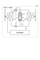
- FIG. 1 is a diagram showing a configuration example of a refrigeration cycle device according to a first embodiment
- FIG. 2 is a diagram showing a configuration example of a power conversion device according to a first embodiment provided in the refrigeration cycle device shown in FIG.
- FIG. 1 is a diagram showing a configuration example of a rectification unit provided in a power conversion device according to a first embodiment
- FIG. 1 is a first diagram illustrating an operation of a power conversion device according to a first embodiment of the present invention
- FIG. 2 is a second diagram illustrating the operation of the power conversion device according to the first embodiment.
- FIG. 11 is a front view showing the configuration of an outdoor unit constituting a refrigeration cycle device according to a second embodiment.
- FIG. 7 is a diagram for explaining the air flow inside the housing of the outdoor unit shown in FIG. 6 .
- FIG. 3 is a diagram showing a configuration of a first modified example of a rectification unit provided in the power conversion device shown in FIG. 2 .
- FIG. 3 is a diagram showing a configuration of a second modified example of a rectification unit provided in the power conversion device shown in FIG. 2 .
- FIG. 3 is a diagram showing a configuration of a third modified example of a rectification unit provided in the power conversion device shown in FIG. 2 .
- FIG. 4 is a diagram showing a configuration of a fourth modified example of a rectification unit provided in the power conversion device shown in FIG. FIG.
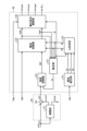
- FIG. 13 is a diagram showing a configuration example of a power conversion device according to a fourth embodiment
- FIG. 13 is a diagram showing the configuration of a motor control unit and a load pulsation compensation unit shown in FIG. 12
- FIG. 13 is a diagram showing a configuration example of a synchronous PWM control unit shown in FIG. 12
- FIG. 13 is a diagram showing an example of a hardware configuration for implementing a control unit included in a power conversion device according to a fourth embodiment.
- FIG. 13 is a diagram for explaining current flowing in and out of a smoothing capacitor provided in a power conversion device according to a fifth embodiment. A diagram showing the current flow that causes deterioration of a smoothing capacitor as a comparative example.
- FIG. 13 is a diagram showing the configuration example of a power conversion device according to a fourth embodiment
- FIG. 13 is a diagram showing the configuration of a motor control unit and a load pulsation compensation unit shown in FIG. 12 .
- FIG. 13 is a diagram showing
- FIG. 13 is a diagram for explaining a power supply pulsation compensation control function in a power conversion device according to a fifth embodiment.
- FIG. 13 is a diagram showing a configuration example of a power conversion device according to a sixth embodiment; 13 is a flowchart for explaining the operation of the waveform shape change control performed by the power conversion device according to the sixth embodiment.
- FIG. 1 is a diagram showing a configuration example of a refrigeration cycle device 150 according to a first embodiment.
- the refrigeration cycle device 150 can be used in an air conditioner, a heat pump water heater, a refrigerator, a freezer, and the like.
- the refrigeration cycle device 150 includes a compressor 60, a four-way valve 102, an outdoor unit heat exchanger 103, an expansion mechanism 104, and an indoor unit heat exchanger 105. These components are connected in sequence via a refrigerant pipe 106 to form a refrigeration cycle.
- the compressor 60 includes a compression mechanism 107 that compresses the refrigerant, and a compressor motor 61 that operates the compression mechanism 107.
- the compressor 60 is a fluid machine that draws in low-pressure gas refrigerant, compresses it, and discharges it as high-pressure gas refrigerant.
- various types of compressors such as reciprocating, rotary, scroll, or screw compressors are used.
- the refrigeration cycle device 150 also includes an outdoor fan 109 for passing air through the outdoor unit heat exchanger 103, an outdoor unit fan motor 110 for driving the outdoor fan 109, an indoor fan 111 for passing air through the indoor unit heat exchanger 105, and an indoor unit fan motor 112 for driving the indoor fan 111.
- An example of the outdoor fan 109 is a propeller fan
- an example of the indoor fan 111 is a centrifugal fan or a crossflow fan.
- the power conversion device 100 drives the compressor motor 61 connected to the compressor 60 and the outdoor unit fan motor 110 connected to the outdoor fan 109. Specifically, the power conversion device 100 drives the compressor motor 61 and the outdoor unit fan motor 110 by converting the power supply voltage applied from an AC power supply not shown in FIG. 1 into a drive voltage to the compressor motor 61 and the outdoor unit fan motor 110. Note that the drive device that drives the indoor unit fan motor 112 is not shown in FIG. 1.
- FIG. 2 is a diagram showing an example of the configuration of the power conversion device 100 according to the first embodiment provided in the refrigeration cycle device 150 shown in FIG. 1.
- the power conversion device 100 shown in FIG. 1 drives the compressor motor 61 and the fan motor 65 by converting the power supply voltage applied from the AC power supply 50 into a drive voltage for the compressor motor 61 connected to the compressor 60 and the fan motor 65 connected to the fan 64, which is an outdoor fan.
- the midpoint 54 of the AC power supply 50 is grounded to the earth potential 51.
- the earth potential 51 is the potential of a ground wire or ground surface not shown, and is the reference potential of the power supply voltage.
- the AC power supply 50 may be a single-phase two-wire system, a three-phase three-wire system, or a three-phase four-wire system.
- the power distribution system of the AC power supply 50 is determined according to the specifications of the refrigeration cycle device 150
- the power conversion device 100 includes a noise filter 11, a rectifier 12, a smoothing capacitor 13, inverters 15 and 17, and a canceller 80.
- the noise filter 11 is a passive filter composed of passive elements such as an inductor and a capacitor.
- the noise filter 11 is electrically connected to an earth potential 52.
- the noise filter 11 is disposed between an AC power source 50 and the rectifier 12, and operates to reduce noise currents flowing in and out of the power conversion device 100.
- the rectifier 12 rectifies the power supply voltage applied from the AC power source 50.
- the smoothing capacitor 13 is disposed between a DC bus 71 and a DC bus 72, which are electrical wiring for electrically connecting the rectifier 12 and the inverters 15 and 17, and smoothes and holds the rectified voltage rectified by the rectifier 12.
- the inverters 15 and 17 are conversion units that convert the rectified voltage rectified by the rectifier 12 into a drive voltage for each load.
- the inverter 15 includes multiple switching elements 14, and converts the rectified voltage rectified by the rectifier 12 into a drive voltage for the compressor motor 61 to drive the compressor motor 61.
- the inverter 17 includes multiple switching elements 16, and converts the rectified voltage rectified by the rectifier 12 into a drive voltage for the fan 64 to drive the fan motor 65.
- the canceller 80 also includes a detection unit 20, a compensation signal generation unit 30, and an injection unit 40.
- the detection unit 20 includes a first coil 21 and a second coil 22 that is magnetically coupled to the first coil 21.
- the first coil 21 includes two windings 21a and 21b.
- the winding 21a is arranged on the power line 18, and the winding 22a is arranged on the power line 19.
- the power lines 18 and 19 are electrical wiring for electrically connecting the noise filter 11 and the rectification unit 12.
- the second coil 22 includes two windings 22a and 22b, each of which is magnetically coupled to the winding 21b.
- the black circles in the figure are symbols indicating the polarity of the voltage generated in each winding.
- the compensation signal generating unit 30 includes termination resistors 31 and 32, gate resistors 33 and 34, and voltage-driven elements 35 and 36.
- the termination resistor 31, gate resistor 33, and voltage-driven element 35 are provided to correspond to the winding 22a, and the termination resistor 32, gate resistor 34, and voltage-driven element 36 are provided to correspond to the winding 22b.
- An example of the voltage-driven elements 35 and 36 is the illustrated MOSFET (Metal-Oxide-Semiconductor Field-Effect Transistor), but voltage-driven elements other than MOSFETs may also be used.
- the injection unit 40 includes a resistor 41 and a capacitor 42 connected in series to the resistor 41.
- the injection unit 40 is electrically connected to earth potential 52. Note that in FIG. 2, the connection order of the resistor 41 and the capacitor 42 in the injection unit 40 may be reversed from that shown in the figure. That is, the resistor 41 may be disposed on the side of the earth potential 52. Also, the injection unit 40 does not need to include both the resistor 41 and the capacitor 42, and it is sufficient if it includes at least one of the resistor 41 and the capacitor 42.
- the inverter 15 or the inverter 17 When the inverter 15 or the inverter 17 performs a switching operation, the inverter 15 or the inverter 17 generates power. At this time, the inverter 15 or the inverter 17 becomes a noise source, that is, a source of noise power, and a common mode current flows inside the power conversion device 100.
- the common mode current here means a leakage current that flows through the parasitic capacitance 62 between the compressor 60 and the earth potential 63. Since the common mode current flows inside the power conversion device 100, it also flows through the power lines 18 and 19.
- the windings 22a and 22b of the detection unit 20 detect a physical quantity that is correlated with the common mode current flowing through the power lines 18 and 19.
- the detection voltage of the winding 22a is generated across the termination resistor 31, and the voltage of the termination resistor 31 is applied to the voltage-driven element 35 via the gate resistor 33.
- the detection voltage of the winding 22a is a physical quantity that is correlated with the common mode current.
- the voltage-driven element 35 When the voltage of the termination resistor 31 exceeds the threshold voltage of the voltage-driven element 35, the voltage-driven element 35 becomes conductive. When the voltage-driven element 35 becomes conductive, the connection point 37 between the voltage-driven element 35 and the voltage-driven element 36 is electrically connected to the high-potential DC bus 71 via the conductive voltage-driven element 35, and a compensation current flows from the connection point 37 toward the earth potential 52 via the injection unit 40. This direction cancels out the common mode current, and the compensation current flowing via the injection unit 40 reduces the common mode current.
- the detection voltage of winding 22b is generated across termination resistor 32, and the voltage of termination resistor 32 is applied to voltage-driven element 36 via gate resistor 34.
- voltage-driven element 36 becomes conductive.
- connection point 37 is electrically connected to low-potential DC bus 72 via conductive voltage-driven element 36, and a compensation current flows from earth potential 52 toward connection point 37 via injection unit 40.
- This direction is the opposite to when voltage-driven element 35 is conductive, but because winding 22a and winding 22b are connected with opposite polarity, this direction cancels out the common mode current. Therefore, even when voltage-driven element 36 is conductive, the common mode current is reduced by the compensation current flowing via injection unit 40.
- the detection unit 20 detects a physical quantity that is correlated with the common mode current flowing between the noise filter 11 and the rectification unit 12, and the compensation signal generation unit 30 that generates a compensation current based on the detected physical quantity is connected between the rectification unit 12 and the inverters 15 and 17 that are the noise power supply sources. Therefore, the detection unit 20 and the compensation signal generation unit 30 are configured as a feedback system when viewed from the inverters 15 and 17.
- the detection unit 20 and the compensation signal generation unit 30 can generate compensation currents of both polarities, but even with a compensation current of one polarity, it is possible to reduce the common mode current. Therefore, when a configuration is used to generate a compensation current of one polarity, one of the windings 22a, 22b of the detection unit 20 can be omitted.
- the set of the termination resistor 31, the gate resistor 33, and the voltage-driven element 35 in the compensation signal generation unit 30, and the set of the termination resistor 32, the gate resistor 34, and the voltage-driven element 36 one of the sets of the windings 22a, 22b corresponding to the omitted winding can be omitted.
- FIG. 2 illustrates a configuration in which the compensation signal generating unit 30 generates a compensation current
- the compensation signal generating unit 30 may generate a compensation voltage.
- the compensation voltage generated by the compensation signal generating unit 30 is applied to, for example, the power lines 18 and 19. In this manner, it is possible to reduce the common mode current.
- the detection unit 20 detects a physical quantity that is correlated with the common mode current flowing inside the power conversion device 100 via the earth potential that is the reference for the power supply voltage. Furthermore, the compensation signal generation unit 30 generates a compensation current or compensation voltage as a compensation signal for canceling out the common mode current based on the physical quantity detected by the detection unit 20. Then, the injection unit 40 injects the compensation signal output from the compensation signal generation unit 30 into the earth potential.
- FIG. 3 is a diagram showing an example of the configuration of the rectifier 12 provided in the power conversion device 100 according to the first embodiment.
- Fig. 4 is a first diagram used to explain the operation of the power conversion device 100 according to the first embodiment
- Fig. 5 is a second diagram used to explain the operation of the power conversion device 100 according to the first embodiment.
- FIG. 3 is a circuit diagram showing a typical configuration of the rectifier 12, and shows a full-wave rectifier circuit.
- a full-wave rectifier circuit is configured by connecting four diodes D1 to D4 in a bridge configuration.
- FIGS. 4 and 5 show the operating waveforms of the main parts when the power conversion device 100 generates a compensation signal.
- FIG. 4 shows the operating waveforms under light load conditions
- FIG. 5 shows the operating waveforms under heavy load conditions.
- the dashed line indicates the bus voltage
- the solid line indicates the absolute value of the power supply voltage.
- the bus voltage is the voltage between the DC buses 71 and 72.
- Each upper center part indicates the input current to the rectifier 12.
- Each lower center part indicates the end-to-end voltages Vd1 to Vd4 generated at both ends of the diodes D1 to D4.
- the end-to-end voltages Vd1 to Vd4 refer to the anode side as positive (+) and the cathode side as negative (-).
- Each lower part indicates the common mode current flowing through the power lines 18 and 19.
- the horizontal axis in Figures 4 and 5 indicates time.
- the power supply voltage vertex refers to a section with a certain phase width that includes 90 degrees of the power supply voltage phase. 90 degrees of the power supply voltage phase is the phase where the absolute value of the power supply voltage is at its peak. The phase width varies depending on the load conditions.
- the period during which the input current flows is longer under heavy load conditions than under light load conditions. This is because the fluctuations in the bus voltage are greater under heavy load conditions than under light load conditions.
- the period during which the input current flows is the period during which diodes D1 and D4 or diodes D2 and D3 of the rectifier 12 are conducting, and during this time the voltage across each diode is approximately 0.6 V, which is the forward voltage when each diode is conducting. Note that approximately 0.6 V is an example of a forward voltage, and may vary depending on the characteristics of each diode.
- the resistance values of the termination resistors 31 and 32 in the compensation signal generating unit 30 are set so that a compensation signal is generated at the peak of the power supply voltage.
- the compensation signal is automatically generated by the operation of the detection unit 20 and the compensation signal generating unit 30 without the involvement of the control unit 90 described later. Therefore, it is possible to extremely reduce the time lag between generating and outputting the compensation signal.
- the method of the first embodiment does not use a switch to set whether or not to output the compensation signal, as in Patent Document 1, so it is possible to suppress an increase in loss.
- the refrigeration cycle device includes a compressor and a fan, and a power conversion device that converts the power supply voltage applied from an AC power supply into a drive voltage for a compressor motor connected to the compressor and a fan motor connected to the fan.
- the power conversion device includes a rectifier, a converter, a detector, a compensation signal generator, and an injection unit. The rectifier rectifies the power supply voltage, and the converter converts the rectified voltage rectified by the rectifier into a drive voltage.
- the detector detects a physical quantity that is correlated with the common mode current flowing through the power conversion device via the earth potential that is the reference for the power supply voltage, and the compensation signal generator generates a compensation signal for canceling the common mode current based on the physical quantity detected by the detector, and the injection unit injects the compensation signal into the earth potential.
- the compensation signal generator generates a compensation signal at the peak of the power supply voltage. If a power conversion device configured in this manner is used, the compensation signal is automatically generated by the operation of the detector and the compensation signal generator without the involvement of a control unit or the like. This provides the effect of extremely reducing the time lag between generating and outputting the compensation signal.
- the power conversion device according to embodiment 1 does not use loss components such as switches, which has the effect of suppressing an increase in loss when outputting a compensation signal.
- Fig. 6 is a front view showing a configuration of an outdoor unit 200 that constitutes a refrigeration cycle device 150 according to the second embodiment.
- Fig. 7 is a diagram for explaining an air flow inside a housing 201 of the outdoor unit 200 shown in Fig. 6.
- the outdoor unit 200 has a housing 201 that forms the outer shell of the outdoor unit 200, and the housing 201 has an air outlet 208. Inside the housing 201, there are housed a blower 209 that directs air taken in from outside the housing 201 toward the outlet 208, and a compressor 210 that compresses the refrigerant.
- the blower 209 is located behind the outlet 208.
- the blower 209 has a fan 213 and a fan motor 214 that is the power source for the fan 213.
- the fan 213 rotates as the fan motor 214 is driven, generating an air flow.
- the rear surface 203 and the side surface 204 are provided with openings (not shown) for taking in air from outside the housing 201 into the inside of the housing 201. Air taken in from outside the housing 201 through the openings in the rear surface 203 and the side surface 204 flows toward the air outlet 208. In FIG. 7, the direction of the air flow is indicated by an arrow.
- a board 217 on which electronic components are mounted is housed inside the housing 201.
- Electronic components for driving the compressor 210 and electronic components for driving the blower 209 are mounted on the board 217. These electronic components are housed together with the board 217 in an electrical component box 220.
- the voltage-driven elements 35, 36 provided in the compensation signal generating unit 30 can be mounted on the substrate 217 together with the electronic components that drive the compressor 210 and the blower 209, but may be placed anywhere on the air flow path as shown in FIG. 7. By placing them in such a location, the voltage-driven elements 35, 36 can be cooled efficiently without the need for heat dissipation components, etc.
- the compensation signal generating unit provided in the canceller includes at least one voltage-driven element, and the voltage-driven element is disposed on the path of the airflow generated by the rotation of the fan. This makes it possible to suppress heat generation from the voltage-driven element without providing any heat dissipation components, etc.
- Embodiment 3 In the third embodiment, variations in the configuration of the rectifier 12 will be described with reference to Fig. 8 to Fig. 11.
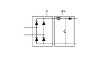
- Fig. 8 to Fig. 11 are diagrams showing the configurations of first to fourth modified examples of the rectifier 12 provided in the power conversion device 100 shown in Fig. 2.
- a boost circuit 12a is provided downstream of the rectifier 12, i.e., between the rectifier 12 and a smoothing capacitor 13 (not shown in FIG. 8).
- the boost circuit 12a it is possible to boost the bus voltage while improving the power factor of the power supply current flowing into the power conversion device 100.
- a reactor 12b is inserted before the rectifier 12, i.e., between the rectifier 12 and the detector 20 (not shown in FIG. 9). Also, in FIG. 9, a short circuit 12c is provided to short the power supply voltage applied to the rectifier 12. By providing the reactor 12b and the short circuit 12c, the bus voltage can be boosted. Furthermore, by providing the reactor 12b, the power factor of the power supply current can be improved.
- a reactor 12b is inserted, and a single-phase bridge circuit 12d is provided in which each of the four diodes constituting the full-wave rectifier circuit is replaced with a switching element.
- the reactor 12b and the single-phase bridge circuit 12d can boost the bus voltage while improving the power factor of the power supply current.
- a reactor 12b is inserted, and a single-phase bridge circuit 12e is provided in which two diodes in one of two sets of diode groups connected in series among the four diodes that make up the full-wave rectifier circuit are replaced with switching elements. Even with the configuration in FIG. 11, it is possible to boost the bus voltage while improving the power factor of the power supply current.
- Air conditioners often incorporate reactors or boost circuits to improve the power factor and boost the bus voltage in response to demands such as harmonic regulations and an expanded operating range.
- boosting the bus voltage increases the common mode current compared to when the bus voltage is not boosted. Therefore, the canceller 80 described in embodiment 1 is useful for air conditioners that have a bus voltage boost function.
- the canceller 80 described in the first embodiment is installed in this type of air conditioner, the voltage-driven elements 35, 36 provided in the canceller 80 are required to be high-voltage products.
- the voltage-driven elements 35, 36 are MOSFETs, high-voltage MOSFETs are easy to obtain, but the higher the voltage, the higher the on-resistance and the greater the tendency for losses to increase.
- the canceller 80 described in the first embodiment does not use loss components such as switches, as mentioned above, so it is possible to suppress the increase in losses when outputting a compensation signal. Therefore, applying the canceller 80 described in the first embodiment to an air conditioner with a bus voltage boost function is particularly useful from the perspective of suppressing the increase in losses.
- the rectifier provided in the power conversion device is configured to be capable of boosting voltage, then by installing the canceller described in embodiment 1, it becomes possible to appropriately comply with harmonic regulations while suppressing losses in the power conversion device.
- Embodiment 4 an application example to a power conversion device 100 having a load pulsation compensation control function will be described.
- the load pulsation compensation control function is a function for suppressing noise of the compressor 60 caused by vibration of the compressor motor 61 by superimposing a current having a frequency correlated with the rotation speed of the compressor motor 61 on the current output by the inverter 15.
- FIG. 12 is a diagram showing an example of the configuration of a power conversion device 100 according to embodiment 4.
- components that are the same as or equivalent to those in FIG. 2 are given the same reference numerals.
- the inverter 17, the fan 64, and the fan motor 65 are not shown.
- the power conversion device 100 includes a smoothing capacitor 13 and an inverter 15, as well as a DC voltage detection unit 82, a current detection unit 84, and a control unit 90.
- the inverter 15 includes switching elements 94a to 94f and diodes 95a to 95f connected in parallel to each of the switching elements 94a to 94f.
- the control unit 90 includes a motor control unit 96, a synchronous PWM (Pulse Width Modulation) control unit 97, and a load pulsation compensation unit 98.
- the DC voltage detection unit 82 detects the voltage across the smoothing capacitor 13 as the bus voltage Vdc.
- the current detection unit 84 detects the DC current Idc flowing through the input side of the inverter 15.
- the control unit 90 also includes a motor control unit 96 that generates a voltage command value, a synchronous PWM control unit 97 that generates synchronous PWM signals UP, VP, WP, UN, VN, and WN, and a load pulsation compensation unit 98 that generates a signal that compensates for load pulsation.
- FIG. 13 is a diagram showing an example of the configuration of the motor control unit 96 and the load pulsation compensation unit 98 shown in FIG. 12.
- the motor control unit 96 includes a current restoration unit 121 that restores the current, a dq conversion unit 122 that converts a three-phase current into a two-phase current and performs a dq conversion of the two-phase current, an estimation unit 123 that estimates the position and speed, a speed control unit 124 that controls the speed, a current control unit 125 that controls the current, and a voltage command calculation unit 126 that generates a voltage command value.
- the current restoration unit 121 restores the phase currents Iu, Iv, and Iw flowing through the compressor motor 61 based on the DC current Idc detected by the current detection unit 84.
- the dq conversion unit 122 converts the three-phase currents Iu, Iv, and Iw into two-phase currents based on the rotor pole position ⁇ of the compressor motor 61, and performs dq conversion on the two-phase currents to a d-axis current Id and a q-axis current Iq on the dq coordinate axes.
- the estimation unit 123 calculates the rotor magnetic pole position ⁇ and the estimated speed value ⁇ of the compressor motor 61 based on the d-axis current Id and the q-axis current Iq, and the d-axis voltage command value Vd* and the q-axis voltage command value Vq* generated by the current control unit 125.
- the speed control unit 124 calculates the q-axis current command value Iq* so that the speed estimate value ⁇ matches the speed command value ⁇ *.
- the current control unit 125 calculates a d-axis voltage command value Vd* such that the d-axis current Id matches the externally input d-axis current command value Id*, and calculates a q-axis voltage command value Vq* such that the q-axis current Iq matches the q-axis current command value Iq*.
- the voltage command calculation unit 126 calculates the voltage command values Vu*, Vv*, and Vw* of the UVW phases based on the d-axis voltage command value Vd*, the q-axis voltage command value Vq*, the bus voltage Vdc detected by the DC voltage detection unit 82, and the rotor pole position ⁇ .
- the load pulsation compensation unit 98 includes a compensation unit 131 that calculates the speed command value compensation amount ⁇ * and the carrier frequency command value compensation amount ⁇ fc*, and an adder 132 that generates the speed command value ⁇ *.
- the compensation unit 131 calculates a speed command value compensation amount ⁇ * and a carrier frequency command value compensation amount ⁇ fc* based on the speed command value ⁇ * (ave) provided by a higher-level controller of the motor control unit 96.
- the compensation unit 131 compensates for the speed command value ⁇ * (ave) using the speed command value compensation amount ⁇ *.
- the compensation unit 131 also compensates for the carrier using the carrier frequency command value compensation amount ⁇ fc*.
- An adder 132 adds the speed command value ⁇ * (ave) and the speed command value compensation amount ⁇ * to generate the speed command value ⁇ *.
- FIG. 14 is a diagram showing an example of the configuration of the synchronous PWM control unit 97 shown in FIG. 12.
- the synchronous PWM control unit 97 includes a carrier generation unit 133 that generates a carrier, and a carrier comparison unit 134 that generates the synchronous PWM signals UP, VP, WP, UN, VN, and WN.
- the carrier generating unit 133 generates a carrier so as to synchronize with the voltage phase ⁇ v generated by the voltage command calculating unit 126.
- the carrier generating unit 133 also compensates the carrier by the carrier frequency command value compensation amount ⁇ fc*.
- the carrier comparator 134 compares the magnitude of the carrier with the voltage command values Vu*, Vv*, and Vw*, and outputs High and Low synchronous PWM signals.
- the power conversion device 100 compensates for the speed command value ⁇ * (ave) by the speed command value compensation amount ⁇ * generated by the load pulsation compensation unit 98, and compensates for the carrier by the carrier frequency command value compensation amount ⁇ fc* generated by the load pulsation compensation unit 98. Therefore, when periodic pulsation occurs in the load connected to the compressor motor 61, the frequency of the synchronous PWM signal output from the synchronous PWM control unit 97 can perform stable synchronous PWM modulation while suppressing the load pulsation.
- FIG. 15 is a diagram showing an example of a hardware configuration for implementing the control unit 90 provided in the power conversion device 100 according to the fourth embodiment.
- the control unit 90 is implemented by a processor 91 and a memory 92.
- the processor 91 is a CPU (also called a Central Processing Unit, central processing unit, processing unit, arithmetic unit, microprocessor, microcomputer, processor, or DSP (Digital Signal Processor)) or a system LSI (Large Scale Integration).
- Examples of the memory 92 include non-volatile or volatile semiconductor memories such as RAM (Random Access Memory), ROM (Read Only Memory), flash memory, EPROM (Erasable Programmable Read Only Memory), and EEPROM (registered trademark) (Electrically Erasable Programmable Read Only Memory).
- the memory 92 is not limited to these, and may be a magnetic disk, optical disk, compact disk, mini disk, or DVD (Digital Versatile Disc).
- Load pulsation compensation control is a technology unique to air conditioners. In load pulsation compensation control, an additional compensation current must be passed in addition to the current required for normal motor control. Therefore, applying the canceller 80 described in embodiment 1 to an air conditioner that performs load pulsation compensation control is particularly useful from the perspective of suppressing an increase in losses.
- the power conversion device is configured to perform load pulsation compensation control in which a current of a frequency correlated with the rotation speed of the compressor motor is superimposed on the current output by the inverter, by installing the canceller described in embodiment 1, it is possible to appropriately comply with harmonic regulations while suppressing losses in the power conversion device and suppressing compressor noise.
- Embodiment 5 an example of application to a power conversion device 100 having a power supply pulsation compensation control function will be described.
- the power supply pulsation compensation control function is a function for suppressing deterioration of the smoothing capacitor 13 by superimposing a current having a frequency correlated with the frequency of the power supply voltage that can flow through the smoothing capacitor 13 on the current output by the inverter 15.
- FIG. 16 is a diagram explaining the current flowing in and out of the smoothing capacitor 13 provided in the power conversion device 100 according to embodiment 5.
- the current flowing from the rectifier 12 to the smoothing capacitor 13 side is current I1
- the current flowing into the inverter 15 is current I2
- the current flowing out from the smoothing capacitor 13 is current I3.
- Current I2 is a combination of current I1 and current I3.
- Current I3 can be expressed as the difference between current I2 and current I1, that is, current I2 - current I1.
- the discharge direction of smoothing capacitor 13 is the positive direction of current I3, and the charge direction of smoothing capacitor 13 is the negative direction.
- FIG. 17 is a diagram showing, as a comparative example, the current flow that causes the deterioration of the smoothing capacitor 13.
- FIG. 18 is a diagram provided for explaining the power supply pulsation compensation control function in the power conversion device 100 according to embodiment 5.
- the upper parts indicate current I1
- the upper middle parts indicate current I2
- the lower middle parts indicate current I3
- the lower parts indicate the bus voltage Vdc.
- the horizontal axis in FIGS. 17 and 18 indicates time. Note that in reality, the carrier component of the inverter 15 is superimposed on currents I2 and I3, but this is omitted here.
- FIG. 18 shows an example of the waveforms of currents I1 to I3 and bus voltage Vdc when the power conversion device 100 according to embodiment 5 controls the operation of the inverter 15 to reduce the current I3 flowing through the smoothing capacitor 13.
- the power conversion device 100 controls the operation of the inverter 15 so that a current I2 including a pulsating current whose main component is the frequency component of the current I1 flows through the inverter 15.
- the pulsating current whose main component is the frequency component of the current I1 referred to here is a current whose frequency is correlated with the frequency of the power supply voltage that can flow through the smoothing capacitor 13.
- the power conversion device when the power conversion device is configured to perform power supply pulsation compensation control in which a current of a frequency correlated with the frequency of the power supply voltage that can flow through the smoothing capacitor is superimposed on the current output by the inverter, by installing the canceller described in embodiment 1, it becomes possible to appropriately respond to harmonic regulations while suppressing losses in the power conversion device and suppressing deterioration of the smoothing capacitor.
- Embodiment 6 an application example to a power conversion device 100 having a waveform shape modification control function will be described.
- the waveform shape modification control function is a function for modifying the waveform shape of the switching waveform of the switching elements provided in the inverters 15, 17.
- the waveform shape modification control function is particularly useful when the air conditioner performs constrained energization.
- Constrained energization is a technique for heating the liquid refrigerant accumulated inside the compressor 60 by applying a high-frequency AC voltage higher than the operating frequency range during compression operation to the three-phase windings of the compressor motor 61.
- FIG. 19 is a diagram showing an example of the configuration of a power conversion device 100 according to embodiment 6.
- components that are the same as or equivalent to those in FIG. 2 and FIG. 12 are given the same reference numerals. Also, in FIG. 19, the inverter 17, the fan 64, and the fan motor 65 are not shown.
- the power conversion device 100 includes a rectifier 12, state quantity detection units 501, 502, 505, and 506, a smoothing capacitor 13, an inverter 15, and a control unit 90.
- the control unit 90 includes a basic pulse generation unit 410 and a waveform shape control signal output unit 420.
- the inverter 15 includes a waveform shape modification unit 340 that can change the waveform shape of the switching waveform of the switching elements 94a to 94f.
- the waveform shape modification unit 340 can output two or more waveform shapes as the waveform shapes of the switching waveform of the switching elements 94a to 94f.
- the state quantity detection unit 501 detects state quantities that indicate the operating state of the power conversion device 100.
- the state quantity detection unit 501 detects, for example, the voltage value of the DC power supplied from the smoothing capacitor 13 to the inverter 15, the current value of the DC power supplied from the smoothing capacitor 13 to the inverter 15, etc.
- the state quantity detection unit 502 detects a state quantity indicating the operating state of the power conversion device 100.
- the state quantity detection unit 502 detects, for example, the voltage value of the AC power supplied from the inverter 15 to the compressor motor 61, and the current value of the AC power supplied from the inverter 15 to the compressor motor 61.
- the state quantity detection unit 505 detects a state quantity indicating the operating state of the power conversion device 100.
- the state quantity detection unit 505 detects, for example, the current value of the DC power supplied from the smoothing capacitor 13 to the inverter 15.
- the state quantity detection unit 506 detects a state quantity indicating the operating state of the power conversion device 100.
- the state quantity detection unit 506 detects, for example, the current flowing through the switching elements 94b, 94d, and 94f.
- the control unit 90 acquires the state quantities detected by the state quantity detection units 501, 502, 505, and 506 from the state quantity detection units 501, 502, 505, and 506, and controls the operation of the inverter 15 based on the acquired state quantities, specifically, controls the on/off of the switching elements 94a to 94f of the inverter 15.
- the basic pulse generating unit 410 calculates a duty ratio according to the state quantities detected by the state quantity detecting units 501, 502, 505, and 506, and generates a basic pulse for controlling the operation of the switching elements 94a to 94f of the inverter 15.
- the basic pulse is, for example, a PWM signal having a duty ratio according to the state quantities detected by the state quantity detecting units 501, 502, 505, and 506.
- the basic pulse generating unit 410 outputs the basic pulse for controlling the operation of the switching elements 94a to 94f of the inverter 15 to the waveform shape control signal output unit 420.
- the waveform shape control signal output unit 420 sets the waveform shape of the switching waveform of the switching elements 94a to 94f when the switching waveform of the switching elements 94a to 94f is changed by the waveform shape change unit 340 of the inverter 15 according to the state quantities detected by the state quantity detection units 501, 502, 505, and 506, and outputs a control signal indicating the set waveform shape.
- the waveform shape control signal output unit 420 controls the magnitude of the drive signal that the waveform shape change unit 340 of the inverter 15 outputs to the switching elements 94a to 94f to actually drive the switching elements 94a to 94f, and the timing of outputting the drive signal.
- the waveform shape control signal output unit 420 outputs a control signal for controlling the operation of the waveform shape change unit 340 to the waveform shape change unit 340.
- the compressor motor 61 rotates according to the amplitude and phase of the AC power supplied from the inverter 15, and performs compression operation.
- the compressor motor 61 is supplied with power for restricting current supply from the inverter 15, and heats the liquid refrigerant accumulated inside the compressor 60.
- the power conversion device 100 can change the waveform shape of the switching waveform of the switching elements 94a to 94f of the inverter 15 by the waveform shape control signal output unit 420 and the waveform shape change unit 340. Specifically, the power conversion device 100 can change the switching speed, delay time, etc., when the switching elements 94a to 94f of the inverter 15 perform a switching operation.
- FIG. 20 is a flowchart explaining the operation of the waveform shape change control performed by the power conversion device 100 according to the sixth embodiment.
- the basic pulse generation unit 410 generates a basic pulse for driving the switching elements 94a to 94f of the inverter 15 based on the state quantities obtained from the state quantity detection units 501, 502, 505, and 506 (step S1).
- the basic pulse generation unit 410 generates a basic pulse based on the state quantities obtained from the state quantity detection units 501, 502, 505, and 506, and determines the timing for turning on and off the switching elements 94a to 94f.
- the basic pulse generation unit 410 outputs the generated basic pulse to the waveform shape control signal output unit 420.
- the waveform shape control signal output unit 420 sets a waveform shape for changing the waveform shape of the switching waveform of the switching elements 94a to 94f of the inverter 15 based on the basic pulse obtained from the basic pulse generation unit 410 and the state quantities obtained from the state quantity detection units 501, 502, 505, and 506. In this way, in the control unit 90, the waveform shape control signal output unit 420 sets the waveform shape of the switching waveform at the timing to turn on and turn off the switching elements 94a to 94f determined by the basic pulse generation unit 410 based on the state quantities obtained from the state quantity detection units 501, 502, 505, and 506.
- the waveform shape control signal output unit 420 outputs a control signal to the waveform shape change unit 340 that can change the magnitude and output timing of the drive signal according to the set waveform shape (step S2).
- the waveform shape modification unit 340 modifies the waveform shape of the gate current to be output to the switching elements 94a to 94f of the inverter 15, i.e., the waveform shape of the switching waveform of the switching elements 94a to 94f, based on the control signal obtained from the waveform shape control signal output unit 420 (step S3).
- the waveform shape modification unit 340 outputs the gate current after the waveform shape modification to the switching elements 94a to 94f of the inverter 15.
- the power conversion device 100 can change the magnitude and output timing of the drive signal for driving the switching elements 94a to 94f of the inverter 15 by using the functions of the basic pulse generating unit 410 and the waveform shape control signal output unit 420 described above.
- the power conversion device 100 When the power conversion device 100 has a waveform shape change control function, the power conversion device 100 may be required to increase the switching speed of the switching elements 94a to 94f in order to improve performance. On the other hand, the faster the switching speed, the greater the common mode current, and therefore the larger the compensation signal must be. Therefore, applying the canceller 80 described in embodiment 1 to an air conditioner that performs waveform shape change control is particularly useful from the perspective of suppressing increases in losses.
- the inverter and control unit provided in the power conversion device are configured to be able to change the waveform shape of the switching waveform of the switching element, by installing the canceller described in embodiment 1, it becomes possible to appropriately comply with harmonic regulations while suppressing losses in the power conversion device.
Landscapes
- Engineering & Computer Science (AREA)
- Power Engineering (AREA)
- Inverter Devices (AREA)
Priority Applications (3)
| Application Number | Priority Date | Filing Date | Title |
|---|---|---|---|
| JP2025538969A JPWO2025032691A1 (https=) | 2023-08-07 | 2023-08-07 | |
| CN202380100919.5A CN121693851A (zh) | 2023-08-07 | 2023-08-07 | 制冷循环装置 |
| PCT/JP2023/028777 WO2025032691A1 (ja) | 2023-08-07 | 2023-08-07 | 冷凍サイクル装置 |
Applications Claiming Priority (1)
| Application Number | Priority Date | Filing Date | Title |
|---|---|---|---|
| PCT/JP2023/028777 WO2025032691A1 (ja) | 2023-08-07 | 2023-08-07 | 冷凍サイクル装置 |
Publications (1)
| Publication Number | Publication Date |
|---|---|
| WO2025032691A1 true WO2025032691A1 (ja) | 2025-02-13 |
Family
ID=94534371
Family Applications (1)
| Application Number | Title | Priority Date | Filing Date |
|---|---|---|---|
| PCT/JP2023/028777 Pending WO2025032691A1 (ja) | 2023-08-07 | 2023-08-07 | 冷凍サイクル装置 |
Country Status (3)
| Country | Link |
|---|---|
| JP (1) | JPWO2025032691A1 (https=) |
| CN (1) | CN121693851A (https=) |
| WO (1) | WO2025032691A1 (https=) |
Citations (4)
| Publication number | Priority date | Publication date | Assignee | Title |
|---|---|---|---|---|
| JP2005033895A (ja) * | 2003-07-10 | 2005-02-03 | Toshiba Corp | 電力変換装置 |
| JP2019187176A (ja) * | 2018-04-16 | 2019-10-24 | サンデン・オートモーティブコンポーネント株式会社 | 電力変換装置 |
| JP6906731B1 (ja) * | 2020-02-17 | 2021-07-21 | 三菱電機株式会社 | ノイズ抑制装置 |
| JP2023051880A (ja) * | 2021-09-30 | 2023-04-11 | ダイキン工業株式会社 | ノイズ低減回路、負荷システム、電力変換装置及び冷凍装置 |
-
2023
- 2023-08-07 WO PCT/JP2023/028777 patent/WO2025032691A1/ja active Pending
- 2023-08-07 JP JP2025538969A patent/JPWO2025032691A1/ja active Pending
- 2023-08-07 CN CN202380100919.5A patent/CN121693851A/zh active Pending
Patent Citations (4)
| Publication number | Priority date | Publication date | Assignee | Title |
|---|---|---|---|---|
| JP2005033895A (ja) * | 2003-07-10 | 2005-02-03 | Toshiba Corp | 電力変換装置 |
| JP2019187176A (ja) * | 2018-04-16 | 2019-10-24 | サンデン・オートモーティブコンポーネント株式会社 | 電力変換装置 |
| JP6906731B1 (ja) * | 2020-02-17 | 2021-07-21 | 三菱電機株式会社 | ノイズ抑制装置 |
| JP2023051880A (ja) * | 2021-09-30 | 2023-04-11 | ダイキン工業株式会社 | ノイズ低減回路、負荷システム、電力変換装置及び冷凍装置 |
Also Published As
| Publication number | Publication date |
|---|---|
| CN121693851A (zh) | 2026-03-17 |
| JPWO2025032691A1 (https=) | 2025-02-13 |
Similar Documents
| Publication | Publication Date | Title |
|---|---|---|
| US8169180B2 (en) | Motor controller of air conditioner | |
| KR20150141085A (ko) | 모터 구동장치 및 이를 구비하는 공기조화기 | |
| JP4033628B2 (ja) | 電源装置及びその電源装置を用いた空気調和機 | |
| JP7459308B2 (ja) | 電力変換装置、モータ駆動装置及び冷凍サイクル適用機器 | |
| CN116897498A (zh) | 电力转换装置、马达驱动装置以及空调机 | |
| WO2022149207A1 (ja) | 電力変換装置、モータ駆動装置及び冷凍サイクル適用機器 | |
| KR101936631B1 (ko) | 모터 구동장치 및 이를 구비하는 공기조화기 | |
| JP7566175B2 (ja) | 電力変換装置、電動機駆動装置及び冷凍サイクル適用機器 | |
| KR102043950B1 (ko) | 전력변환장치 및 이를 포함하는 공기조화기 | |
| KR20140112297A (ko) | 전력변환장치, 및 이를 구비하는 공기조화기 | |
| JP7507894B2 (ja) | 電力変換装置、モータ駆動装置及び冷凍サイクル適用機器 | |
| KR20150074754A (ko) | 모터 구동장치 및 이를 구비하는 공기조화기 | |
| US20240405694A1 (en) | Power converting apparatus, motor drive unit, and refrigeration cycle-incorporating device | |
| KR20140108956A (ko) | 전력변환장치 및 이를 포함하는 공기조화기 | |
| JP2004364492A (ja) | モータ駆動装置及び空気調和装置 | |
| WO2025032691A1 (ja) | 冷凍サイクル装置 | |
| JP7542751B2 (ja) | 電力変換装置、電動機駆動装置及び冷凍サイクル適用機器 | |
| CN116783810A (zh) | 电力转换装置、马达驱动装置以及制冷循环应用设备 | |
| KR20210092540A (ko) | 전력 변환 장치 및 이를 이용하는 공기 조화기 | |
| JP7566174B2 (ja) | 電力変換装置、電動機駆動装置及び冷凍サイクル適用機器 | |
| JP7278497B2 (ja) | 電力変換装置および空気調和機 | |
| WO2023095311A1 (ja) | 電力変換装置、電動機駆動装置及び冷凍サイクル適用機器 | |
| KR20160026529A (ko) | 모터 구동장치 및 이를 구비하는 공기조화기 | |
| KR20160043433A (ko) | 모터 구동장치 및 이를 구비하는 공기조화기 | |
| JP7825794B1 (ja) | 電力変換装置、モータ駆動装置および冷凍サイクル適用機器 |
Legal Events
| Date | Code | Title | Description |
|---|---|---|---|
| 121 | Ep: the epo has been informed by wipo that ep was designated in this application |
Ref document number: 23948411 Country of ref document: EP Kind code of ref document: A1 |
|
| ENP | Entry into the national phase |
Ref document number: 2025538969 Country of ref document: JP Kind code of ref document: A |
|
| WWE | Wipo information: entry into national phase |
Ref document number: 2025538969 Country of ref document: JP |