WO2025018348A1 - 信号伝達装置、電子機器及び車両 - Google Patents
信号伝達装置、電子機器及び車両 Download PDFInfo
- Publication number
- WO2025018348A1 WO2025018348A1 PCT/JP2024/025526 JP2024025526W WO2025018348A1 WO 2025018348 A1 WO2025018348 A1 WO 2025018348A1 JP 2024025526 W JP2024025526 W JP 2024025526W WO 2025018348 A1 WO2025018348 A1 WO 2025018348A1
- Authority
- WO
- WIPO (PCT)
- Prior art keywords
- signal
- pulses
- potential
- insulating layer
- pulse
- Prior art date
- Legal status (The legal status is an assumption and is not a legal conclusion. Google has not performed a legal analysis and makes no representation as to the accuracy of the status listed.)
- Pending
Links
Images








Classifications
-
- H—ELECTRICITY
- H03—ELECTRONIC CIRCUITRY
- H03K—PULSE TECHNIQUE
- H03K17/00—Electronic switching or gating, i.e. not by contact-making and –breaking
- H03K17/51—Electronic switching or gating, i.e. not by contact-making and –breaking characterised by the components used
- H03K17/56—Electronic switching or gating, i.e. not by contact-making and –breaking characterised by the components used by the use, as active elements, of semiconductor devices
- H03K17/687—Electronic switching or gating, i.e. not by contact-making and –breaking characterised by the components used by the use, as active elements, of semiconductor devices the devices being field-effect transistors
- H03K17/689—Electronic switching or gating, i.e. not by contact-making and –breaking characterised by the components used by the use, as active elements, of semiconductor devices the devices being field-effect transistors with galvanic isolation between the control circuit and the output circuit
- H03K17/691—Electronic switching or gating, i.e. not by contact-making and –breaking characterised by the components used by the use, as active elements, of semiconductor devices the devices being field-effect transistors with galvanic isolation between the control circuit and the output circuit using transformer coupling
-
- H—ELECTRICITY
- H03—ELECTRONIC CIRCUITRY
- H03K—PULSE TECHNIQUE
- H03K19/00—Logic circuits, i.e. having at least two inputs acting on one output; Inverting circuits
- H03K19/0175—Coupling arrangements; Interface arrangements
-
- H—ELECTRICITY
- H03—ELECTRONIC CIRCUITRY
- H03K—PULSE TECHNIQUE
- H03K7/00—Modulating pulses with a continuously-variable modulating signal
- H03K7/08—Duration or width modulation ; Duty cycle modulation
-
- H—ELECTRICITY
- H04—ELECTRIC COMMUNICATION TECHNIQUE
- H04L—TRANSMISSION OF DIGITAL INFORMATION, e.g. TELEGRAPHIC COMMUNICATION
- H04L25/00—Baseband systems
- H04L25/02—Details ; arrangements for supplying electrical power along data transmission lines
Definitions
- the present disclosure provides a signal transmission device configured to have a transmitter configured to receive an input signal and output a primary side transmission pulse signal having a number of pulses determined according to the input signal every time a predetermined first time period elapses, and a receiver configured to receive a secondary side transmission pulse signal having the same number of pulses as the primary side transmission pulse signal by performing insulated communication with the transmitter, obtain the number of pulses contained in the secondary side transmission pulse signal, and output an output signal according to the number of pulses.
- FIG. 1 is a diagram showing a basic configuration of a signal transmission device.
- FIG. 2 is a diagram showing the basic structure of a transformer chip.
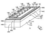
- FIG. 3 is a perspective view of a semiconductor device used as a two-channel type transformer chip.
- FIG. 4 is a plan view of the semiconductor device shown in FIG.
- FIG. 5 is a plan view showing a layer in which the low potential coil is formed in the semiconductor device of FIG.
- FIG. 6 is a plan view showing a layer in which a high potential coil is formed in the semiconductor device of FIG.
- FIG. 7 is a cross-sectional view taken along line VIII-VIII shown in FIG.
- FIG. 8 is an enlarged view (isolation structure) of the region XIII shown in FIG.
- FIG. 9 is a diagram illustrating an example of the layout of a transformer chip.
- FIG. 10 is a diagram illustrating an embodiment of a signal transmission device.
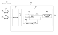
- FIG. 11 is a diagram showing an example of the configuration of a receiving section including a signal output circuit.
- FIG. 12 is a timing chart showing an example of a signal state during operation of the signal transmission device.
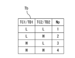
- 13 is a diagram showing an example of a conversion table for converting an input signal into a primary side transmission pulse signal.
- FIG. 14 is a diagram showing an example of the operation of the signal transmission device when the input signal is switched.
- FIG. 15 is a timing chart showing another example of the switching timing of the primary side transmission pulse signal.
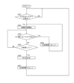
- FIG. 16 is a flowchart showing an example of the operation of the signal transmission device of the first modified example.
- FIG. 17 is a timing chart showing an example of the operation of the signal transmission device of the second modified example.
- FIG. 18 is a flowchart showing the operation of the signal transmission device of the second modified example
- the signal transmission device 200 of this configuration example is a semiconductor integrated circuit device (so-called insulated gate driver IC) that transmits a pulse signal from the primary circuit system 200p to the secondary circuit system 200s while isolating the primary circuit system 200p (VCC1-GND1 system) from the secondary circuit system 200s (VCC2-GND2 system) and drives the gate of a switch element (not shown) provided in the secondary circuit system 200s.
- the signal transmission device 200 is formed by sealing a controller chip 210, a driver chip 220, and a transformer chip 230 in a single package.
- the controller chip 210 is a semiconductor chip that operates by receiving a power supply voltage VCC1 (for example, up to 7 V based on GND1).
- the controller chip 210 includes, for example, a pulse transmission circuit 211 and buffers 212 and 213 integrated therein.
- the pulse transmission circuit 211 is a pulse generator that generates the transmission pulse signals S11 and S21 in response to the input pulse signal IN. More specifically, when the pulse transmission circuit 211 notifies that the input pulse signal IN is at a high level, it pulse drives the transmission pulse signal S11 (outputs a single or multiple transmission pulses), and when it notifies that the input pulse signal IN is at a low level, it pulse drives the transmission pulse signal S21. In other words, the pulse transmission circuit 211 pulse drives either the transmission pulse signal S11 or S21 in response to the logical level of the input pulse signal IN.
- the buffer 212 receives the transmission pulse signal S11 from the pulse transmission circuit 211 and pulse-drives the transformer chip 230 (specifically, the transformer 231).
- the buffer 213 receives the transmission pulse signal S21 from the pulse transmission circuit 211 and pulse-drives the transformer chip 230 (specifically, the transformer 232).
- the driver chip 220 is a semiconductor chip that operates by receiving a power supply voltage VCC2 (for example, up to 30 V based on GND2).
- the driver chip 220 includes, for example, buffers 221 and 222, a pulse receiving circuit 223, and a driver 224.
- the buffer 221 shapes the waveform of the received pulse signal S12 induced in the transformer chip 230 (specifically, the transformer 231) and outputs it to the pulse receiving circuit 223.
- the buffer 222 shapes the waveform of the received pulse signal S22 induced in the transformer chip 230 (specifically, the transformer 232) and outputs it to the pulse receiving circuit 223.
- the pulse receiving circuit 223 generates the output pulse signal OUT by driving the driver 224 in response to the received pulse signals S12 and S22 input via the buffers 221 and 222. More specifically, the pulse receiving circuit 223 drives the driver 224 so as to raise the output pulse signal OUT to a high level in response to the pulse drive of the received pulse signal S12, and to lower the output pulse signal OUT to a low level in response to the pulse drive of the received pulse signal S22. In other words, the pulse receiving circuit 223 switches the logical level of the output pulse signal OUT in response to the logical level of the input pulse signal IN.
- an RS flip-flop can be suitably used as the pulse receiving circuit 223.
- the driver 224 generates an output pulse signal OUT based on the drive control of the pulse receiving circuit 223.
- the transformer chip 230 uses transformers 231 and 232 to provide DC insulation between the controller chip 210 and the driver chip 220, and outputs the transmission pulse signals S11 and S21 input from the pulse transmission circuit 211 to the pulse reception circuit 223 as reception pulse signals S12 and S22, respectively.
- DC insulation means that the objects to be insulated are not connected by a conductor.
- the transformer 231 outputs a received pulse signal S12 from the secondary coil 231s in response to a transmitted pulse signal S11 input to the primary coil 231p.
- the transformer 232 outputs a received pulse signal S22 from the secondary coil 232s in response to a transmitted pulse signal S21 input to the primary coil 232p.
- the input pulse signal IN is separated into two transmission pulse signals S11 and S21 (corresponding to the rise signal and fall signal), and then transmitted from the primary circuit system 200p to the secondary circuit system 200s via the two transformers 231 and 232.
- the signal transmission device 200 of this configuration example has an independent transformer chip 230 equipped with only transformers 231 and 232, in addition to the controller chip 210 and driver chip 220, and these three chips are sealed in a single package.
- the controller chip 210 and the driver chip 220 can both be formed using a general low to medium voltage process (withstands a few volts to several tens of volts), eliminating the need to use a dedicated high voltage process (withstands a few kV), making it possible to reduce manufacturing costs.
- the signal transmission device 200 can be suitably used, for example, in a power supply device or a motor drive device for on-board equipment mounted in a vehicle.
- the above vehicles include not only engine vehicles, but also electric vehicles (BEVs [battery electric vehicles], HEVs [hybrid electric vehicles], PHEVs/PHVs (plug-in hybrid electric vehicles/plug-in hybrid vehicles), or xEVs such as FCEVs/FCVs (fuel cell electric vehicles/fuel cell vehicles)).
- FIG. 2 is a diagram showing the basic structure of the transformer chip 230.
- the transformer 231 includes a primary coil 231p and a secondary coil 231s that face each other in the vertical direction.
- the transformer 232 includes a primary coil 232p and a secondary coil 232s that face each other in the vertical direction.
- the primary coils 231p and 232p are both formed on the first wiring layer (lower layer) 230a of the transformer chip 230.
- the secondary coils 231s and 232s are both formed on the second wiring layer (upper layer in this figure) 230b of the transformer chip 230.
- the secondary coil 231s is disposed directly above the primary coil 231p and faces the primary coil 231p.
- the secondary coil 232s is disposed directly above the primary coil 232p and faces the primary coil 232p.
- the primary coil 231p is laid in a spiral shape starting from a first end connected to the internal terminal X21, surrounding the internal terminal X21 in a clockwise direction, and its second end corresponding to its end point is connected to the internal terminal X22.
- the primary coil 232p is laid in a spiral shape starting from a first end connected to the internal terminal X23, surrounding the internal terminal X23 in a counterclockwise direction, and its second end corresponding to its end point is connected to the internal terminal X22.
- the internal terminals X21, X22, and X23 are linearly arranged in the order shown.
- the internal terminal X21 is connected to the external terminal T21 of the second layer 230b via the conductive wiring Y21 and via Z21.
- the internal terminal X22 is connected to the external terminal T22 of the second layer 230b via the conductive wiring Y22 and via Z22.
- the internal terminal X23 is connected to the external terminal T23 of the second layer 230b via the conductive wiring Y23 and via Z23.
- the external terminals T21 to T23 are arranged in a straight line and are used for wire bonding with the controller chip 210.
- the secondary coil 231s is laid in a spiral shape starting from a first end connected to the external terminal T24, surrounding the external terminal T24 in a counterclockwise direction, and its second end corresponding to its end point is connected to the external terminal T25.
- the secondary coil 232s is laid in a spiral shape starting from a first end connected to the external terminal T26, surrounding the external terminal T26 in a clockwise direction, and its second end corresponding to its end point is connected to the external terminal T25.
- the external terminals T24, T25, and T26 are arranged linearly in the order shown in the figure, and are used for wire bonding with the driver chip 220.
- Secondary coils 231s and 232s are AC-connected to primary coils 231p and 232p by magnetic coupling, and are DC-insulated from primary coils 231p and 232p, respectively. That is, driver chip 220 is AC-connected to controller chip 210 via transformer chip 230, and is DC-insulated from controller chip 210 by transformer chip 230.
- FIG. 3 is a perspective view showing a semiconductor device 5 used as a two-channel transformer chip.
- FIG. 4 is a plan view of the semiconductor device 5 shown in FIG. 3.
- FIG. 5 is a plan view showing a layer in which a low-potential coil 22 (corresponding to a primary coil of a transformer) is formed in the semiconductor device 5 shown in FIG. 3.
- FIG. 6 is a plan view showing a layer in which a high-potential coil 23 (corresponding to a secondary coil of a transformer) is formed in the semiconductor device 5 shown in FIG. 3.
- FIG. 7 is a cross-sectional view taken along line VIII-VIII shown in FIG. 6.
- FIG. 8 is an enlarged view of region XIII shown in FIG. 7, showing an isolation structure 130.
- the semiconductor device 5 includes a semiconductor chip 41 having a rectangular parallelepiped shape.
- the semiconductor chip 41 includes at least one of silicon, a wide band gap semiconductor, and a compound semiconductor.
- a wide bandgap semiconductor is made of a semiconductor whose bandgap exceeds that of silicon (approximately 1.12 eV).
- the bandgap of a wide bandgap semiconductor is preferably 2.0 eV or more.
- the wide bandgap semiconductor may be SiC (silicon carbide).
- the compound semiconductor may be a III-V compound semiconductor.
- the compound semiconductor may include at least one of AlN (aluminum nitride), InN (indium nitride), GaN (gallium nitride), and GaAs (gallium arsenide).
- the semiconductor chip 41 includes a semiconductor substrate made of silicon.
- the semiconductor chip 41 may be an epitaxial substrate having a layered structure including a semiconductor substrate made of silicon and an epitaxial layer made of silicon.
- the conductivity type of the semiconductor substrate may be n-type or p-type.
- the epitaxial layer may be n-type or p-type.
- the semiconductor chip 41 has a first main surface 42 on one side, a second main surface 43 on the other side, and chip sidewalls 44A-44D connecting the first main surface 42 and the second main surface 43.
- the first main surface 42 and the second main surface 43 are formed in a quadrangular shape (rectangular in this embodiment) when viewed in a plan view from their normal direction Z (hereinafter simply referred to as "plan view").
- the chip sidewalls 44A to 44D include a first chip sidewall 44A, a second chip sidewall 44B, a third chip sidewall 44C, and a fourth chip sidewall 44D.
- the first chip sidewall 44A and the second chip sidewall 44B form the long sides of the semiconductor chip 41.
- the first chip sidewall 44A and the second chip sidewall 44B extend along the first direction X and face the second direction Y.
- the third chip sidewall 44C and the fourth chip sidewall 44D form the short sides of the semiconductor chip 41.
- the third chip sidewall 44C and the fourth chip sidewall 44D extend in the second direction Y and face the first direction X.
- the chip sidewalls 44A to 44D are made of ground surfaces.
- the semiconductor device 5 further includes an insulating layer 51 formed on the first main surface 42 of the semiconductor chip 41.
- the insulating layer 51 has an insulating main surface 52 and insulating side walls 53A-53D.
- the insulating main surface 52 is formed in a quadrangular shape (rectangular in this embodiment) that matches the first main surface 42 in a plan view.
- the insulating main surface 52 extends parallel to the first main surface 42.
- the insulating sidewalls 53A to 53D include a first insulating sidewall 53A, a second insulating sidewall 53B, a third insulating sidewall 53C, and a fourth insulating sidewall 53D.
- the insulating sidewalls 53A to 53D extend from the periphery of the insulating main surface 52 toward the semiconductor chip 41 and are continuous with the chip sidewalls 44A to 44D. Specifically, the insulating sidewalls 53A to 53D are formed flush with the chip sidewalls 44A to 44D.
- the insulating sidewalls 53A to 53D form a ground surface that is flush with the chip sidewalls 44A to 44D.
- the insulating layer 51 is made of a multi-layer insulating laminate structure including a bottom insulating layer 55, a top insulating layer 56, and a plurality of (11 in this embodiment) interlayer insulating layers 57.
- the bottom insulating layer 55 is an insulating layer that directly covers the first main surface 42.
- the top insulating layer 56 is an insulating layer that forms the insulating main surface 52.
- the plurality of interlayer insulating layers 57 are insulating layers interposed between the bottom insulating layer 55 and the top insulating layer 56.
- the bottom insulating layer 55 has a single-layer structure including silicon oxide.
- the top insulating layer 56 has a single-layer structure including silicon oxide.
- the thickness of the bottom insulating layer 55 and the top insulating layer 56 may each be 1 ⁇ m or more and 3 ⁇ m or less (for example, about 2 ⁇ m).
- the multiple interlayer insulating layers 57 each have a stacked structure including a first insulating layer 58 on the bottom insulating layer 55 side and a second insulating layer 59 on the top insulating layer 56 side.
- the first insulating layer 58 may include silicon nitride.
- the first insulating layer 58 is formed as an etching stopper layer for the second insulating layer 59.
- the thickness of the first insulating layer 58 may be 0.1 ⁇ m or more and 1 ⁇ m or less (for example, about 0.3 ⁇ m).
- the second insulating layer 59 is formed on the first insulating layer 58. It contains an insulating material different from that of the first insulating layer 58.
- the second insulating layer 59 may contain silicon oxide.
- the thickness of the second insulating layer 59 may be 1 ⁇ m or more and 3 ⁇ m or less (for example, about 2 ⁇ m). It is preferable that the thickness of the second insulating layer 59 exceeds the thickness of the first insulating layer 58.
- the total thickness DT of the insulating layers 51 may be 5 ⁇ m or more and 50 ⁇ m or less.
- the total thickness DT of the insulating layers 51 and the number of layers of the interlayer insulating layers 57 are arbitrary and are adjusted according to the dielectric strength voltage (dielectric breakdown resistance) to be achieved.
- the insulating materials of the bottom insulating layer 55, the top insulating layer 56 and the interlayer insulating layer 57 are arbitrary and are not limited to a specific insulating material.
- the semiconductor device 5 includes a first functional device 45 formed in an insulating layer 51.
- the first functional device 45 includes one or more (in this embodiment, multiple) transformers 21 (corresponding to the aforementioned transformer).
- the semiconductor device 5 is a multi-channel device including multiple transformers 21.
- the multiple transformers 21 are formed in the inner part of the insulating layer 51 at intervals from the insulating side walls 53A-53D.
- the multiple transformers 21 are formed at intervals in the first direction X.
- the multiple transformers 21 specifically include a first transformer 21A, a second transformer 21B, a third transformer 21C, and a fourth transformer 21D, which are formed in this order from the insulating side wall 53C side to the insulating side wall 53D side in a plan view.
- the multiple transformers 21A to 21D each have a similar structure.
- the structure of the first transformer 21A will be explained as an example.
- the explanation of the structures of the second transformer 21B, third transformer 21C, and fourth transformer 21D will be omitted, as the explanation of the structure of the first transformer 21A applies mutatis mutandis.
- the first transformer 21A includes a low-potential coil 22 and a high-potential coil 23.
- the low-potential coil 22 is formed in an insulating layer 51.
- the high-potential coil 23 is formed in the insulating layer 51 so as to face the low-potential coil 22 in the normal direction Z.
- the low-potential coil 22 and the high-potential coil 23 are formed in a region sandwiched between the bottom insulating layer 55 and the top insulating layer 56 (i.e., multiple interlayer insulating layers 57).
- the low-potential coil 22 is formed on the bottom insulating layer 55 (semiconductor chip 41) side within the insulating layer 51, and the high-potential coil 23 is formed on the top insulating layer 56 (insulating main surface 52) side of the low-potential coil 22 within the insulating layer 51.
- the high-potential coil 23 faces the semiconductor chip 41 with the low-potential coil 22 in between.
- the low-potential coil 22 and the high-potential coil 23 may be positioned at any location. Furthermore, it is sufficient that the high-potential coil 23 faces the low-potential coil 22 with one or more interlayer insulating layers 57 in between.
- the distance between the low potential coil 22 and the high potential coil 23 (i.e., the number of layers of the interlayer insulating layer 57) is adjusted appropriately according to the dielectric strength and electric field strength between the low potential coil 22 and the high potential coil 23.
- the low potential coil 22 is formed in the third interlayer insulating layer 57 counting from the bottom insulating layer 55 side.
- the high potential coil 23 is formed in the first interlayer insulating layer 57 counting from the top insulating layer 56 side.
- the low-potential coil 22 is embedded in the interlayer insulating layer 57, penetrating the first insulating layer 58 and the second insulating layer 59.
- the low-potential coil 22 includes a first inner end 24, a first outer end 25, and a first spiral portion 26 wound in a spiral shape between the first inner end 24 and the first outer end 25.
- the first spiral portion 26 is wound in a spiral shape that extends in an elliptical shape (oval shape) in a plan view.
- the portion that forms the innermost edge of the first spiral portion 26 defines a first inner region 66 that is elliptical in a plan view.
- the number of turns of the first spiral portion 26 may be 5 or more and 30 or less.
- the width of the first spiral portion 26 may be 0.1 ⁇ m or more and 5 ⁇ m or less.
- the width of the first spiral portion 26 is preferably 1 ⁇ m or more and 3 ⁇ m or less.
- the width of the first spiral portion 26 is defined by the width in a direction perpendicular to the spiral direction.
- the first winding pitch of the first spiral portion 26 may be 0.1 ⁇ m or more and 5 ⁇ m or less.
- the first winding pitch is preferably 1 ⁇ m or more and 3 ⁇ m or less.
- the first winding pitch is defined by the distance between two adjacent portions of the first spiral portion 26 in a direction perpendicular to the spiral direction.
- the winding shape of the first spiral portion 26 and the planar shape of the first inner region 66 are arbitrary and are not limited to the form shown in FIG. 5, etc.
- the first spiral portion 26 may be wound in a polygonal shape, such as a triangular shape or a rectangular shape, or in a circular shape in a planar view.
- the first inner region 66 may be partitioned into a polygonal shape, such as a triangular shape or a rectangular shape, or in a circular shape in a planar view, depending on the winding shape of the first spiral portion 26.
- the low potential coil 22 may include at least one of titanium, titanium nitride, copper, aluminum, and tungsten.
- the low potential coil 22 may have a laminated structure including a barrier layer and a main body layer.
- the barrier layer defines a recess space in the interlayer insulating layer 57.
- the barrier layer may include at least one of titanium and titanium nitride.
- the main body layer may include at least one of copper, aluminum, and tungsten.
- the high-potential coil 23 is embedded in the interlayer insulating layer 57, penetrating the first insulating layer 58 and the second insulating layer 59.
- the high-potential coil 23 includes a second inner end 27, a second outer end 28, and a second spiral portion 29 wound in a spiral shape between the second inner end 27 and the second outer end 28.
- the second spiral portion 29 is wound in a spiral shape extending in an elliptical shape (oval shape) in a planar view.
- the portion forming the innermost periphery of the second spiral portion 29 defines a second inner region 67 that is elliptical in a planar view.
- the second inner region 67 of the second spiral portion 29 faces the first inner region 66 of the first spiral portion 26 in the normal direction Z.
- the number of turns of the second spiral portion 29 may be 5 or more and 30 or less.
- the number of turns of the second spiral portion 29 relative to the number of turns of the first spiral portion 26 is adjusted according to the voltage value to be boosted. It is preferable that the number of turns of the second spiral portion 29 exceeds the number of turns of the first spiral portion 26.
- the number of turns of the second spiral portion 29 may be less than the number of turns of the first spiral portion 26, or may be equal to the number of turns of the first spiral portion 26.
- the width of the second spiral portion 29 may be 0.1 ⁇ m or more and 5 ⁇ m or less.
- the width of the second spiral portion 29 is preferably 1 ⁇ m or more and 3 ⁇ m or less.
- the width of the second spiral portion 29 is defined by the width in a direction perpendicular to the spiral direction.
- the width of the second spiral portion 29 is preferably equal to the width of the first spiral portion 26.
- the second winding pitch of the second spiral portion 29 may be 0.1 ⁇ m or more and 5 ⁇ m or less.
- the second winding pitch is preferably 1 ⁇ m or more and 3 ⁇ m or less.
- the second winding pitch is defined by the distance between two adjacent portions of the second spiral portion 29 in a direction perpendicular to the spiral direction.
- the second winding pitch is preferably equal to the first winding pitch of the first spiral portion 26.
- the winding shape of the second spiral portion 29 and the planar shape of the second inner region 67 are arbitrary and are not limited to the form shown in FIG. 6, etc.
- the second spiral portion 29 may be wound in a polygonal shape, such as a triangular shape or a rectangular shape, or in a circular shape in a planar view.
- the second inner region 67 may be partitioned into a polygonal shape, such as a triangular shape or a rectangular shape, or in a circular shape in a planar view, depending on the winding shape of the second spiral portion 29.
- the high-potential coil 23 is preferably formed from the same conductive material as the low-potential coil 22.
- the high-potential coil 23 preferably includes a barrier layer and a main body layer, similar to the low-potential coil 22.
- the semiconductor device 5 includes a plurality (12 in this figure) of low potential terminals 11 and a plurality (12 in this figure) of high potential terminals 12.
- the plurality of low potential terminals 11 are each electrically connected to the low potential coils 22 of the corresponding transformers 21A to 21D.
- the plurality of high potential terminals 12 are each electrically connected to the high potential coils 23 of the corresponding transformers 21A to 21D.
- the low-potential terminals 11 are formed on the insulating main surface 52 of the insulating layer 51. Specifically, the low-potential terminals 11 are formed in an area on the insulating sidewall 53B side at intervals in the second direction Y from the transformers 21A-21D, and are arranged at intervals in the first direction X.
- the low potential terminals 11 include a first low potential terminal 11A, a second low potential terminal 11B, a third low potential terminal 11C, a fourth low potential terminal 11D, a fifth low potential terminal 11E, and a sixth low potential terminal 11F.
- two of each of the low potential terminals 11A to 11F are formed.
- the number of low potential terminals 11A to 11F is arbitrary.
- the first low potential terminal 11A faces the first transformer 21A in the second direction Y in a plan view.
- the second low potential terminal 11B faces the second transformer 21B in the second direction Y in a plan view.
- the third low potential terminal 11C faces the third transformer 21C in the second direction Y in a plan view.
- the fourth low potential terminal 11D faces the fourth transformer 21D in the second direction Y in a plan view.
- the fifth low potential terminal 11E is formed in the area between the first low potential terminal 11A and the second low potential terminal 11B in a plan view.
- the sixth low potential terminal 11F is formed in the area between the third low potential terminal 11C and the fourth low potential terminal 11D in a plan view.
- the first low potential terminal 11A is electrically connected to the first inner end 24 of the first transformer 21A (low potential coil 22).
- the second low potential terminal 11B is electrically connected to the first inner end 24 of the second transformer 21B (low potential coil 22).
- the third low potential terminal 11C is electrically connected to the first inner end 24 of the third transformer 21C (low potential coil 22).
- the fourth low potential terminal 11D is electrically connected to the first inner end 24 of the fourth transformer 21D (low potential coil 22).
- the fifth low potential terminal 11E is electrically connected to the first outer end 25 of the first transformer 21A (low potential coil 22) and the first outer end 25 of the second transformer 21B (low potential coil 22).
- the sixth low potential terminal 11F is electrically connected to the first outer end 25 of the third transformer 21C (low potential coil 22) and the first outer end 25 of the fourth transformer 21D (low potential coil 22).
- the multiple high potential terminals 12 are formed on the insulating main surface 52 of the insulating layer 51 at intervals from the multiple low potential terminals 11. Specifically, the multiple high potential terminals 12 are formed in the area on the insulating sidewall 53A side at intervals from the multiple low potential terminals 11 in the second direction Y, and are arranged at intervals in the first direction X.
- the multiple high potential terminals 12 are each formed in an area close to the corresponding transformer 21A-21D in a planar view.
- the high potential terminals 12 being close to the transformers 21A-21D means that the distance between the high potential terminal 12 and the transformer 21 in a planar view is less than the distance between the low potential terminal 11 and the high potential terminal 12.
- the multiple high potential terminals 12 are formed at intervals along the first direction X so as to face the multiple transformers 21A to 21D along the first direction X in a plan view. More specifically, the multiple high potential terminals 12 are formed at intervals along the first direction X so as to be located in the second inner region 67 of the high potential coil 23 and in the region between adjacent high potential coils 23 in a plan view. As a result, the multiple high potential terminals 12 are arranged in a row with the multiple transformers 21A to 21D in the first direction X in a plan view.
- the multiple high potential terminals 12 include a first high potential terminal 12A, a second high potential terminal 12B, a third high potential terminal 12C, a fourth high potential terminal 12D, a fifth high potential terminal 12E, and a sixth high potential terminal 12F.
- a first high potential terminal 12A a second high potential terminal 12B
- a third high potential terminal 12C a third high potential terminal 12C
- a fourth high potential terminal 12D a fifth high potential terminal 12E
- a sixth high potential terminal 12F a sixth high potential terminal 12F.
- two of each of the multiple high potential terminals 12A to 12F are formed.
- the number of multiple high potential terminals 12A to 12F is arbitrary.
- the first high potential terminal 12A is formed in the second inner region 67 of the first transformer 21A (high potential coil 23) in a plan view.
- the second high potential terminal 12B is formed in the second inner region 67 of the second transformer 21B (high potential coil 23) in a plan view.
- the third high potential terminal 12C is formed in the second inner region 67 of the third transformer 21C (high potential coil 23) in a plan view.
- the fourth high potential terminal 12D is formed in the second inner region 67 of the fourth transformer 21D (high potential coil 23) in a plan view.
- the fifth high potential terminal 12E is formed in the region between the first transformer 21A and the second transformer 21B in a plan view.
- the sixth high potential terminal 12F is formed in the region between the third transformer 21C and the fourth transformer 21D in a plan view.
- the first high potential terminal 12A is electrically connected to the second inner end 27 of the first transformer 21A (high potential coil 23).
- the second high potential terminal 12B is electrically connected to the second inner end 27 of the second transformer 21B (high potential coil 23).
- the third high potential terminal 12C is electrically connected to the second inner end 27 of the third transformer 21C (high potential coil 23).
- the fourth high potential terminal 12D is electrically connected to the second inner end 27 of the fourth transformer 21D (high potential coil 23).
- the fifth high potential terminal 12E is electrically connected to the second outer end 28 of the first transformer 21A (high potential coil 23) and the second outer end 28 of the second transformer 21B (high potential coil 23).
- the sixth high potential terminal 12F is electrically connected to the second outer end 28 of the third transformer 21C (high potential coil 23) and the second outer end 28 of the fourth transformer 21D (high potential coil 23).
- the semiconductor device 5 includes a first low potential wiring 31, a second low potential wiring 32, a first high potential wiring 33, and a second high potential wiring 34, each formed in an insulating layer 51.
- a plurality of first low potential wirings 31, a plurality of second low potential wirings 32, a plurality of first high potential wirings 33, and a plurality of second high potential wirings 34 are formed.
- the first low-potential wiring 31 and the second low-potential wiring 32 fix the low-potential coil 22 of the first transformer 21A and the low-potential coil 22 of the second transformer 21B to the same potential.
- the first low-potential wiring 31 and the second low-potential wiring 32 also fix the low-potential coil 22 of the third transformer 21C and the low-potential coil 22 of the fourth transformer 21D to the same potential.
- the first low-potential wiring 31 and the second low-potential wiring 32 fix all the low-potential coils 22 of the transformers 21A to 21D to the same potential.
- the first high-potential wiring 33 and the second high-potential wiring 34 fix the high-potential coil 23 of the first transformer 21A and the high-potential coil 23 of the second transformer 21B to the same potential.
- the first high-potential wiring 33 and the second high-potential wiring 34 also fix the high-potential coil 23 of the third transformer 21C and the high-potential coil 23 of the fourth transformer 21D to the same potential.
- the first high-potential wiring 33 and the second high-potential wiring 34 fix all the high-potential coils 23 of the transformers 21A to 21D to the same potential.
- the multiple first low potential wirings 31 are electrically connected to the corresponding low potential terminals 11A to 11D and the first inner ends 24 of the corresponding transformers 21A to 21D (low potential coils 22).
- the multiple first low potential wirings 31 have the same structure.
- the structure of the first low potential wiring 31 connected to the first low potential terminal 11A and the first transformer 21A will be described as an example.
- the structure of the other first low potential wirings 31 will be omitted, as the description of the structure of the first low potential wiring 31 connected to the first transformer 21A applies mutatis mutandis.
- the first low-potential wiring 31 includes a through wiring 71, a low-potential connection wiring 72, a lead-out wiring 73, a first connection plug electrode 74, a second connection plug electrode 75, one or more (in this embodiment, multiple) pad plug electrodes 76, and one or more (in this embodiment, multiple) substrate plug electrodes 77.
- the through wiring 71, the low-potential connection wiring 72, the draw-out wiring 73, the first connection plug electrode 74, the second connection plug electrode 75, the pad plug electrode 76, and the substrate plug electrode 77 are preferably each formed from the same conductive material as the low-potential coil 22, etc.
- the through wiring 71, the low-potential connection wiring 72, the draw-out wiring 73, the first connection plug electrode 74, the second connection plug electrode 75, the pad plug electrode 76, and the substrate plug electrode 77 each preferably include a barrier layer and a main body layer, similar to the low-potential coil 22, etc.
- the through wiring 71 penetrates the multiple interlayer insulating layers 57 in the insulating layer 51 and extends in a columnar shape extending along the normal direction Z.
- the through wiring 71 is formed in the region between the bottom insulating layer 55 and the top insulating layer 56 in the insulating layer 51.
- the through wiring 71 has an upper end on the top insulating layer 56 side and a lower end on the bottom insulating layer 55 side.
- the upper end of the through wiring 71 is formed in the same interlayer insulating layer 57 as the high potential coil 23 and is covered by the top insulating layer 56.
- the lower end of the through wiring 71 is formed in the same interlayer insulating layer 57 as the low potential coil 22.
- the through wiring 71 includes a first electrode layer 78, a second electrode layer 79, and a plurality of wiring plug electrodes 80.
- the first electrode layer 78, the second electrode layer 79, and the wiring plug electrodes 80 are each formed from the same conductive material as the low potential coil 22, etc.
- the first electrode layer 78, the second electrode layer 79, and the wiring plug electrodes 80 each include a barrier layer and a main body layer, similar to the low potential coil 22, etc.
- the first electrode layer 78 forms the upper end of the through-wire 71.
- the second electrode layer 79 forms the lower end of the through-wire 71.
- the first electrode layer 78 is formed in an island shape and faces the low potential terminal 11 (first low potential terminal 11A) in the normal direction Z.
- the second electrode layer 79 is formed in an island shape and faces the first electrode layer 78 in the normal direction Z.
- the multiple wiring plug electrodes 80 are embedded in multiple interlayer insulating layers 57 located in the region between the first electrode layer 78 and the second electrode layer 79.
- the multiple wiring plug electrodes 80 are stacked from the bottom insulating layer 55 toward the top insulating layer 56 so as to be electrically connected to each other, and electrically connect the first electrode layer 78 and the second electrode layer 79.
- the multiple wiring plug electrodes 80 each have a planar area less than the planar area of the first electrode layer 78 and the planar area of the second electrode layer 79.
- the number of layers of the multiple wiring plug electrodes 80 matches the number of layers of the multiple interlayer insulating layers 57. In this embodiment, six wiring plug electrodes 80 are embedded in each interlayer insulating layer 57, but the number of wiring plug electrodes 80 embedded in each interlayer insulating layer 57 is arbitrary. Of course, one or more wiring plug electrodes 80 may be formed penetrating the multiple interlayer insulating layers 57.
- the low-potential connection wiring 72 is formed in the first inner region 66 of the first transformer 21A (low-potential coil 22) in the same interlayer insulating layer 57 as the low-potential coil 22.
- the low-potential connection wiring 72 is formed in an island shape and faces the high-potential terminal 12 (first high-potential terminal 12A) in the normal direction Z. It is preferable that the low-potential connection wiring 72 has a planar area that exceeds the planar area of the wiring plug electrode 80.
- the low-potential connection wiring 72 is electrically connected to the first inner end 24 of the low-potential coil 22.
- the draw-out wiring 73 is formed in the interlayer insulating layer 57 in the region between the semiconductor chip 41 and the through wiring 71.
- the draw-out wiring 73 is formed in the first interlayer insulating layer 57 counting from the bottom insulating layer 55.
- the draw-out wiring 73 includes a first end on one side, a second end on the other side, and a wiring portion connecting the first end and the second end.
- the first end of the draw-out wiring 73 is located in the region between the semiconductor chip 41 and the lower end of the through wiring 71.
- the second end of the draw-out wiring 73 is located in the region between the semiconductor chip 41 and the low-potential connection wiring 72.
- the wiring portion extends along the first main surface 42 of the semiconductor chip 41 and extends in a strip shape in the region between the first end and the second end.
- the first connection plug electrode 74 is formed in the region between the through wiring 71 and the draw-out wiring 73 in the interlayer insulating layer 57, and is electrically connected to first ends of the through wiring 71 and the draw-out wiring 73.
- the second connection plug electrode 75 is formed in the region between the low-potential connection wiring 72 and the draw-out wiring 73 in the interlayer insulating layer 57, and is electrically connected to second ends of the low-potential connection wiring 72 and the draw-out wiring 73.
- the multiple pad plug electrodes 76 are formed in the uppermost insulating layer 56 in a region between the low potential terminal 11 (first low potential terminal 11A) and the through wiring 71, and are electrically connected to the upper ends of the low potential terminal 11 and the through wiring 71, respectively.
- the multiple substrate plug electrodes 77 are formed in the lowermost insulating layer 55 in a region between the semiconductor chip 41 and the draw-out wiring 73. In this embodiment, the substrate plug electrodes 77 are formed in a region between the semiconductor chip 41 and the first ends of the draw-out wiring 73, and are electrically connected to the semiconductor chip 41 and the first ends of the draw-out wiring 73, respectively.
- the multiple first high potential wirings 33 are electrically connected to the corresponding high potential terminals 12A-12D and the second inner ends 27 of the corresponding transformers 21A-21D (high potential coils 23).
- the multiple first high potential wirings 33 each have a similar structure.
- the structure of the first high potential wiring 33 connected to the first high potential terminal 12A and the first transformer 21A will be described as an example.
- the structure of the other first high potential wirings 33 will be omitted, as the description of the structure of the first high potential wiring 33 connected to the first transformer 21A applies mutatis mutandis.
- the first high-potential wiring 33 includes a high-potential connection wiring 81 and one or more (in this embodiment, multiple) pad plug electrodes 82.
- the high-potential connection wiring 81 and the pad plug electrode 82 are preferably formed from the same conductive material as the low-potential coil 22, etc.
- the high-potential connection wiring 81 and the pad plug electrode 82 preferably include a barrier layer and a main body layer, similar to the low-potential coil 22, etc.
- the high-potential connection wiring 81 is formed in the second inner region 67 of the high-potential coil 23 in the same interlayer insulating layer 57 as the high-potential coil 23.
- the high-potential connection wiring 81 is formed in an island shape and faces the high-potential terminal 12 (first high-potential terminal 12A) in the normal direction Z.
- the high-potential connection wiring 81 is electrically connected to the second inner end 27 of the high-potential coil 23.
- the high-potential connection wiring 81 is formed at a distance from the low-potential connection wiring 72 in a plan view and does not face the low-potential connection wiring 72 in the normal direction Z. This increases the insulation distance between the low-potential connection wiring 72 and the high-potential connection wiring 81, and increases the dielectric strength of the insulating layer 51.
- the multiple pad plug electrodes 82 are formed in the uppermost insulating layer 56 in a region between the high potential terminal 12 (first high potential terminal 12A) and the high potential connection wiring 81, and are electrically connected to the high potential terminal 12 and the high potential connection wiring 81, respectively.
- the multiple pad plug electrodes 82 each have a planar area less than the planar area of the high potential connection wiring 81 in a plan view.
- the distance D1 between the low potential terminal 11 and the high potential terminal 12 is preferably greater than the distance D2 between the low potential coil 22 and the high potential coil 23 (D2 ⁇ D1).
- the distance D1 is preferably greater than the total thickness DT of the multiple interlayer insulating layers 57 (DT ⁇ D1).
- the ratio D2/D1 of the distance D2 to the distance D1 may be 0.01 or more and 0.1 or less.
- the distance D1 is preferably 100 ⁇ m or more and 500 ⁇ m or less.
- the distance D2 may be 1 ⁇ m or more and 50 ⁇ m or less.
- the distance D2 is preferably 5 ⁇ m or more and 25 ⁇ m or less.
- the values of the distance D1 and the distance D2 are arbitrary and are adjusted appropriately according to the dielectric strength voltage to be realized.
- the semiconductor device 5 includes a dummy pattern 85 embedded in the insulating layer 51 so as to be positioned around the transformers 21A to 21D in a plan view.
- the dummy pattern 85 is formed in a pattern (discontinuous pattern) different from the high potential coil 23 and the low potential coil 22, and is independent of the transformers 21A to 21D. In other words, the dummy pattern 85 does not function as a transformer 21A to 21D.
- the dummy pattern 85 is formed as a shield conductor layer that shields the electric field between the low potential coil 22 and the high potential coil 23 in the transformers 21A to 21D and suppresses electric field concentration on the high potential coil 23.
- the dummy pattern 85 is routed with a line density per unit area equal to the line density of the high potential coil 23.
- the line density of the dummy pattern 85 being equal to the line density of the high potential coil 23 means that the line density of the dummy pattern 85 falls within a range of ⁇ 20% of the line density of the high potential coil 23.
- the depth position of the dummy pattern 85 inside the insulating layer 51 is arbitrary and is adjusted according to the electric field strength to be relaxed.
- the dummy pattern 85 is preferably formed in a region closer to the high potential coil 23 than to the low potential coil 22 in the normal direction Z. Note that the dummy pattern 85 being closer to the high potential coil 23 in the normal direction Z means that the distance between the dummy pattern 85 and the high potential coil 23 in the normal direction Z is less than the distance between the dummy pattern 85 and the low potential coil 22.
- the dummy pattern 85 is preferably formed in the same interlayer insulating layer 57 as the high-potential coil 23. In this case, electric field concentration on the high-potential coil 23 can be further appropriately suppressed.
- the dummy pattern 85 includes multiple dummy patterns with different electrical states.
- the dummy pattern 85 may include a high-potential dummy pattern.
- the depth position of the high-potential dummy pattern 86 inside the insulating layer 51 is arbitrary and is adjusted according to the electric field strength to be relaxed.
- the high-potential dummy pattern 86 is preferably formed in a region closer to the high-potential coil 23 than the low-potential coil 22 in the normal direction Z.
- the high-potential dummy pattern 86 being closer to the high-potential coil 23 in the normal direction Z means that the distance between the high-potential dummy pattern 86 and the high-potential coil 23 in the normal direction Z is less than the distance between the high-potential dummy pattern 86 and the low-potential coil 22.
- the dummy pattern 85 includes a floating dummy pattern formed in an electrically floating state within the insulating layer 51 so as to be positioned around the transformers 21A to 21D.
- the floating dummy pattern is routed in dense lines so as to partially cover and partially expose the area around the high-potential coil 23 in a plan view.
- the floating dummy pattern may be formed with ends or without ends.
- the depth position of the floating dummy pattern inside the insulating layer 51 is arbitrary and is adjusted according to the electric field strength to be mitigated.
- the number of floating lines is arbitrary and is adjusted according to the electric field to be mitigated.
- the floating dummy pattern may be composed of multiple floating lines.
- the semiconductor device 5 includes a second functional device 60 formed on the first main surface 42 of the semiconductor chip 41 in a device region 62.
- the second functional device 60 is formed using a surface portion of the first main surface 42 of the semiconductor chip 41 and/or a region above the first main surface 42 of the semiconductor chip 41, and is covered by an insulating layer 51 (lowest insulating layer 55).
- the second functional device 60 is shown in a simplified form by a dashed line drawn on the surface portion of the first main surface 42.
- the second functional device 60 is electrically connected to the low potential terminal 11 via a low potential wiring, and is electrically connected to the high potential terminal 12 via a high potential wiring.
- the low potential wiring has a structure similar to that of the first low potential wiring 31 (second low potential wiring 32), except that it is routed within the insulating layer 51 so as to be connected to the second functional device 60.
- the high potential wiring has a structure similar to that of the first high potential wiring 33 (second high potential wiring 34), except that it is routed within the insulating layer 51 so as to be connected to the second functional device 60.
- a specific description of the low potential wiring and high potential wiring related to the second functional device 60 will be omitted.
- the second functional device 60 may include at least one of a passive device, a semiconductor rectifier device, and a semiconductor switching device.
- the second functional device 60 may include a circuit network in which any two or more types of devices selected from the passive device, the semiconductor rectifier device, and the semiconductor switching device are selectively combined.
- the circuit network may form part or all of an integrated circuit.
- the passive device may include a semiconductor passive device.
- the passive device may include either or both of a resistor and a capacitor.
- the semiconductor rectifier device may include at least one of a pn junction diode, a PIN diode, a Zener diode, a Schottky barrier diode, and a fast recovery diode.
- the semiconductor switching device may include at least one of a BJT [Bipolar Junction Transistor], a MISFET [Metal Insulator Semiconductor Field Effect Transistor], an IGBT [Insulated Gate Bipolar Junction Transistor], and a JFET [Junction Field Effect Transistor].
- the semiconductor device 5 further includes a seal conductor 61 embedded in the insulating layer 51.
- the seal conductor 61 is embedded in the insulating layer 51 in a wall shape at a distance from the insulating side walls 53A to 53D in a plan view, and divides the insulating layer 51 into a device region 62 and an outer region 63.
- the seal conductor 61 prevents moisture and cracks from entering the device region 62 from the outer region 63.
- the device region 62 is an area including the first functional device 45 (multiple transformers 21), the second functional device 60, multiple low potential terminals 11, multiple high potential terminals 12, the first low potential wiring 31, the second low potential wiring 32, the first high potential wiring 33, the second high potential wiring 34, and the dummy pattern 85.
- the outer region 63 is an area outside the device region 62.
- the seal conductor 61 is electrically isolated from the device region 62. Specifically, the seal conductor 61 is electrically isolated from the first functional device 45 (multiple transformers 21), the second functional device 60, the multiple low potential terminals 11, the multiple high potential terminals 12, the first low potential wiring 31, the second low potential wiring 32, the first high potential wiring 33, the second high potential wiring 34, and the dummy pattern 85. More specifically, the seal conductor 61 is fixed in an electrically floating state. The seal conductor 61 does not form a current path leading to the device region 62.
- the seal conductor 61 is formed in a band shape along the insulating side walls 53 to 53D in a plan view.
- the seal conductor 61 is formed in a square ring shape (specifically, a rectangular ring shape) in a plan view.
- the seal conductor 61 defines a square-shaped (specifically, rectangular) device region 62 in a plan view.
- the seal conductor 61 also defines a square-shaped (specifically, rectangular) outer region 63 that surrounds the device region 62 in a plan view.
- the seal conductor 61 has an upper end on the insulating principal surface 52 side, a lower end on the semiconductor chip 41 side, and a wall extending in a wall shape between the upper end and the lower end.
- the upper end of the seal conductor 61 is formed at a distance from the insulating principal surface 52 to the semiconductor chip 41 side, and is located within the insulating layer 51.
- the upper end of the seal conductor 61 is covered by the uppermost insulating layer 56.
- the upper end of the seal conductor 61 may be covered by one or more interlayer insulating layers 57.
- the upper end of the seal conductor 61 may be exposed from the uppermost insulating layer 56.
- the lower end of the seal conductor 61 is formed at a distance from the semiconductor chip 41 toward the upper end side.
- the seal conductor 61 is embedded in the insulating layer 51 so as to be located on the semiconductor chip 41 side relative to the multiple low potential terminals 11 and multiple high potential terminals 12. Furthermore, the seal conductor 61 faces the first functional device 45 (multiple transformers 21), the first low potential wiring 31, the second low potential wiring 32, the first high potential wiring 33, the second high potential wiring 34, and the dummy pattern 85 in the insulating layer 51 in a direction parallel to the insulating principal surface 52.
- the seal conductor 61 may face a part of the second functional device 60 in the insulating layer 51 in a direction parallel to the insulating principal surface 52.
- the seal conductor 61 includes a plurality of seal plug conductors 64 and one or more (in this embodiment, multiple) seal via conductors 65.
- the number of seal via conductors 65 is arbitrary.
- the uppermost seal plug conductor 64 among the plurality of seal plug conductors 64 forms the upper end of the seal conductor 61.
- the plurality of seal via conductors 65 each form the lower end of the seal conductor 61.
- the seal plug conductor 64 and the seal via conductor 65 are preferably formed from the same conductive material as the low potential coil 22. In other words, the seal plug conductor 64 and the seal via conductor 65 preferably include a barrier layer and a main body layer, similar to the low potential coil 22, etc.
- the multiple seal plug conductors 64 are embedded in the multiple interlayer insulating layers 57, and are each formed in a square ring shape (specifically, a rectangular ring shape) surrounding the device region 62 in a planar view.
- the multiple seal plug conductors 64 are stacked from the bottom insulating layer 55 to the top insulating layer 56 so as to be connected to each other.
- the number of stacked layers of the multiple seal plug conductors 64 matches the number of stacked layers of the multiple interlayer insulating layers 57.
- one or more seal plug conductors 64 may be formed penetrating the multiple interlayer insulating layers 57.
- a single annular seal conductor 61 is formed by an assembly of multiple seal plug conductors 64, it is not necessary for all of the multiple seal plug conductors 64 to be formed in an annular shape.
- at least one of the multiple seal plug conductors 64 may be formed with ends.
- at least one of the multiple seal plug conductors 64 may be divided into multiple strip-shaped portions with ends.
- the multiple seal plug conductors 64 are formed in an endless (annular) shape.
- the multiple seal via conductors 65 are each formed in the area between the semiconductor chip 41 and the seal plug conductor 64 in the bottom insulating layer 55.
- the multiple seal via conductors 65 are formed at a distance from the semiconductor chip 41 and are connected to the seal plug conductor 64.
- the multiple seal via conductors 65 have a planar area less than the planar area of the seal plug conductor 64.
- the single seal via conductor 65 may have a planar area equal to or greater than the planar area of the seal plug conductor 64.
- the width of the sealing conductor 61 may be 0.1 ⁇ m or more and 10 ⁇ m or less.
- the width of the sealing conductor 61 is preferably 1 ⁇ m or more and 5 ⁇ m or less.
- the width of the sealing conductor 61 is defined by the width in a direction perpendicular to the direction in which the sealing conductor 61 extends.
- the semiconductor device 5 further includes an isolation structure 130 that is interposed between the semiconductor chip 41 and the seal conductor 61 and electrically isolates the seal conductor 61 from the semiconductor chip 41.
- the isolation structure 130 preferably includes an insulator.
- the isolation structure 130 is made of a field insulating film 131 formed on the first main surface 42 of the semiconductor chip 41.
- the field insulating film 131 includes at least one of an oxide film (silicon oxide film) and a nitride film (silicon nitride film).
- the field insulating film 131 is preferably made of a low-COS (low-cal oxidation of silicon) film, which is an example of an oxide film formed by oxidizing the first main surface 42 of the semiconductor chip 41.
- the thickness of the field insulating film 131 is arbitrary as long as it can insulate the semiconductor chip 41 and the seal conductor 61.
- the thickness of the field insulating film 131 may be 0.1 ⁇ m or more and 5 ⁇ m or less.
- the isolation structure 130 is formed on the first main surface 42 of the semiconductor chip 41, and extends in a band shape along the seal conductor 61 in a planar view.
- the isolation structure 130 is formed in a square ring shape (specifically, a rectangular ring shape) in a planar view.
- the isolation structure 130 has a connection portion 132 to which the lower end portion (seal via conductor 65) of the seal conductor 61 is connected.
- the connection portion 132 may form an anchor portion in which the lower end portion (seal via conductor 65) of the seal conductor 61 is embedded toward the semiconductor chip 41.
- the connection portion 132 may be formed flush with the main surface of the isolation structure 130.
- the separation structure 130 includes an inner end 130A on the device region 62 side, an outer end 130B on the outer region 63 side, and a main body 130C between the inner end 130A and the outer end 130B.
- the inner end 130A defines the region in which the second functional device 60 is formed (i.e., the device region 62) in a plan view.
- the inner end 130A may be formed integrally with an insulating film (not shown) formed on the first main surface 42 of the semiconductor chip 41.
- the outer end 130B is exposed from the chip sidewalls 44A to 44D of the semiconductor chip 41 and is continuous with the chip sidewalls 44A to 44D of the semiconductor chip 41. More specifically, the outer end 130B is formed flush with the chip sidewalls 44A to 44D of the semiconductor chip 41. The outer end 130B forms a flush ground surface between the chip sidewalls 44A to 44D of the semiconductor chip 41 and the insulating sidewalls 53A to 53D of the insulating layer 51. Of course, in other embodiments, the outer end 130B may be formed in the first main surface 42 at a distance from the chip sidewalls 44A to 44D.
- the main body 130C has a flat surface that extends approximately parallel to the first main surface 42 of the semiconductor chip 41.
- the main body 130C has a connection portion 132 to which the lower end portion (seal via conductor 65) of the seal conductor 61 is connected.
- the connection portion 132 is formed in a portion of the main body 130C that is spaced apart from the inner end portion 130A and the outer end portion 130B.
- the isolation structure 130 can take various forms in addition to the field insulating film 131.
- the semiconductor device 5 further includes an inorganic insulating layer 140 formed on the insulating principal surface 52 of the insulating layer 51 so as to cover the seal conductor 61.
- the inorganic insulating layer 140 may be referred to as a passivation layer.
- the inorganic insulating layer 140 protects the insulating layer 51 and the semiconductor chip 41 from above the insulating principal surface 52.
- the inorganic insulating layer 140 has a laminated structure including a first inorganic insulating layer 141 and a second inorganic insulating layer 142.
- the first inorganic insulating layer 141 may include silicon oxide.
- the first inorganic insulating layer 141 preferably includes USG (undoped silicate glass), which is silicon oxide without added impurities.
- the thickness of the first inorganic insulating layer 141 may be 50 nm or more and 5000 nm or less.
- the second inorganic insulating layer 142 may include silicon nitride.
- the thickness of the second inorganic insulating layer 142 may be 500 nm or more and 5000 nm or less.
- the breakdown voltage (V/cm) of the USG exceeds the breakdown voltage (V/cm) of silicon nitride. Therefore, when thickening the inorganic insulating layer 140, it is preferable to form the first inorganic insulating layer 141 thicker than the second inorganic insulating layer 142.
- the first inorganic insulating layer 141 may contain at least one of BPSG (boron doped phosphor silicate glass) and PSG (phosphorus silicate glass), which are examples of silicon oxide. However, in this case, since impurities (boron or phosphorus) are contained in the silicon oxide, it is particularly preferable to form the first inorganic insulating layer 141 made of USG in order to increase the dielectric strength on the high-potential coil 23.
- the inorganic insulating layer 140 may have a single-layer structure made of either the first inorganic insulating layer 141 or the second inorganic insulating layer 142.
- the inorganic insulating layer 140 covers the entire area of the sealing conductor 61, and has a plurality of low potential pad openings 143 and a plurality of high potential pad openings 144 formed in the area outside the sealing conductor 61.
- the plurality of low potential pad openings 143 expose the plurality of low potential terminals 11, respectively.
- the plurality of high potential pad openings 144 expose the plurality of high potential terminals 12, respectively.
- the inorganic insulating layer 140 may have an overlap portion that rides up on the peripheral portion of the low potential terminal 11.
- the inorganic insulating layer 140 may have an overlap portion that rides up on the peripheral portion of the high potential terminal 12.
- the semiconductor device 5 further includes an organic insulating layer 145 formed on the inorganic insulating layer 140.
- the organic insulating layer 145 may include a photosensitive resin.
- the organic insulating layer 145 may include at least one of polyimide, polyamide, and polybenzoxazole. In this embodiment, the organic insulating layer 145 includes polyimide.
- the thickness of the organic insulating layer 145 may be 1 ⁇ m or more and 50 ⁇ m or less.
- the thickness of the organic insulating layer 145 is preferably greater than the total thickness of the inorganic insulating layer 140. Furthermore, the total thickness of the inorganic insulating layer 140 and the organic insulating layer 145 is preferably greater than or equal to the distance D2 between the low potential coil 22 and the high potential coil 23. In this case, the total thickness of the inorganic insulating layer 140 is preferably greater than or equal to 2 ⁇ m and less than or equal to 10 ⁇ m. Furthermore, the thickness of the organic insulating layer 145 is preferably greater than or equal to 5 ⁇ m and less than or equal to 50 ⁇ m.
- These structures can suppress the thickening of the inorganic insulating layer 140 and the organic insulating layer 145, while at the same time, the laminated film of the inorganic insulating layer 140 and the organic insulating layer 145 can appropriately increase the dielectric strength voltage on the high potential coil 23.
- the organic insulating layer 145 includes a first portion 146 covering the region on the low potential side and a second portion 147 covering the region on the high potential side.
- the first portion 146 covers the seal conductor 61 with the inorganic insulating layer 140 in between.
- the first portion 146 has a plurality of low potential terminal openings 148 that respectively expose a plurality of low potential terminals 11 (low potential pad openings 143) in the region outside the seal conductor 61.
- the first portion 146 may have an overlap portion that rises onto the periphery (overlap portion) of the low potential pad opening 143.
- the second portion 147 is formed at a distance from the first portion 146, exposing the inorganic insulating layer 140 between the second portion 147 and the first portion 146.
- the second portion 147 has a plurality of high potential terminal openings 149 that respectively expose a plurality of high potential terminals 12 (high potential pad openings 144).
- the second portion 147 may have an overlap portion that rises onto the periphery (overlap portion) of the high potential pad opening 144.
- the second portion 147 collectively covers the transformers 21A-21D and the dummy pattern 85. Specifically, the second portion 147 collectively covers the multiple high potential coils 23, the multiple high potential terminals 12, the first high potential dummy pattern 87, the second high potential dummy pattern 88, and the floating dummy pattern 121.
- the embodiments of the present disclosure can be implemented in further different forms.
- an example in which a first functional device 45 and a second functional device 60 are formed has been described.
- a form having only a second functional device 60 without a first functional device 45 may also be adopted.
- the dummy pattern 85 may be removed.
- the second functional device 60 can achieve the same effects as those described in the first embodiment (excluding the effects associated with the dummy pattern 85).
- the second functional device 60 was formed.
- the second functional device 60 is not necessarily required, and may be removed.
- the dummy pattern 85 was formed.
- the dummy pattern 85 is not necessarily required and may be removed.
- the first functional device 45 is a multi-channel type that includes multiple transformers 21.
- a first functional device 45 that is a single-channel type that includes a single transformer 21 may also be used.
- ⁇ Transformer arrangement> 9 is a plan view (top view) showing a schematic example of a transformer arrangement in a two-channel transformer chip 300 (corresponding to the semiconductor device 5 described above).
- the transformer chip 300 in this figure has a first transformer 301, a second transformer 302, a third transformer 303, a fourth transformer 304, a first guard ring 305, a second guard ring 306, pads a1 to a8, pads b1 to b8, pads c1 to c4, and pads d1 to d4.
- pads a1 and b1 are connected to one end of the secondary coil L1s forming the first transformer 301, and pads c1 and d1 are connected to the other end of the secondary coil L1s.
- Pads a2 and b2 are connected to one end of the secondary coil L2s forming the second transformer 302, and pads c1 and d1 are connected to the other end of the secondary coil L2s.
- pads a3 and b3 are connected to one end of the secondary coil L3s forming the third transformer 303, and pads c2 and d2 are connected to the other end of the secondary coil L3s.
- Pads a4 and b4 are connected to one end of the secondary coil L4s forming the fourth transformer 304, and pads c2 and d2 are connected to the other end of the secondary coil L4s.
- the primary coil forming the first transformer 301, the primary coil forming the second transformer 302, the primary coil forming the third transformer 303, and the primary coil forming the fourth transformer 304 are not shown in this diagram.
- the primary coils basically have the same configuration as the secondary coils L1s to L4s, and are arranged directly below each of the secondary coils L1s to L4s, facing the secondary coils L1s to L4s, respectively.
- pads a5 and b5 are connected to one end of the primary coil forming the first transformer 301, and pads c3 and d3 are connected to the other end of the primary coil. Also, pads a6 and b6 are connected to one end of the primary coil forming the second transformer 302, and pads c3 and d3 are connected to the other end of the primary coil.
- pads a7 and b7 are connected to one end of the primary coil forming the third transformer 303, and pads c4 and d4 are connected to the other end of the primary coil.
- pads a8 and b8 are connected to one end of the primary coil forming the fourth transformer 304, and pads c4 and d4 are connected to the other end of the primary coil.
- pads a5 to a8, pads b5 to b8, pads c3 and c4, and pads d3 and d4 are pulled out from the inside of the transformer chip 300 to the surface through vias (not shown).
- pads a1 to a8 correspond to first current supply pads
- pads b1 to b8 correspond to first voltage measurement pads
- pads c1 to c4 correspond to second current supply pads
- pads d1 to d4 correspond to second voltage measurement pads.
- the series resistance component of each coil can be accurately measured during the defective product inspection. This makes it possible to not only reject defective products where each coil has a break in the wire, but also to appropriately reject defective products where the resistance value of each coil is abnormal (for example, a short circuit between coils), which in turn makes it possible to prevent defective products from being released onto the market.
- the above-mentioned multiple pads can be used as a connection means with the primary side chip and the secondary side chip (for example, the aforementioned controller chip 210 and driver chip 220).
- pads a1 and b1, pads a2 and b2, pads a3 and b3, and pads a4 and b4 may be connected to the signal input or output terminals of the secondary chip, respectively.
- Pads c1 and d1, and pads c2 and d2 may be connected to the common voltage application terminal (GND2) of the secondary chip, respectively.
- pads a5 and b5, pads a6 and b6, pads a7 and b7, and pads a8 and b8 may be connected to the signal input or output terminals of the primary chip, respectively.
- pads c3 and d3, and pads c4 and d4 may be connected to the common voltage application terminal (GND1) of the primary chip, respectively.
- the first transformer 301 to the fourth transformer 304 are arranged in a coupled manner according to the respective signal transmission directions.
- the first transformer 301 and the second transformer 302 which transmit signals from the primary chip to the secondary chip are arranged as a first pair by the first guard ring 305.
- the third transformer 303 and the fourth transformer 304, which transmit signals from the secondary chip to the primary chip are arranged as a second pair by the second guard ring 306.
- the reason for this coupling is to ensure a sufficient withstand voltage between the primary coil and the secondary coil when the primary coil and the secondary coil that respectively form the first transformer 301 to the fourth transformer 304 are stacked vertically on the substrate of the transformer chip 300.
- the first guard ring 305 and the second guard ring 306 are not necessarily essential components.
- the first guard ring 305 and the second guard ring 306 may be connected to a low impedance wiring such as a ground terminal via pads e1 and e2, respectively.
- pads c1 and d1 are shared between the secondary coil L1s and secondary coil L2s.
- Pads c2 and d2 are shared between the secondary coil L3s and secondary coil L4s.
- Pads c3 and d3 are shared between the primary coil L1p and primary coil L2p.
- Pads c4 and d4 are shared between the corresponding primary coils. This configuration makes it possible to reduce the number of pads and miniaturize the transformer chip 300.
- transformer arrangement in this diagram is merely one example, and the number, shape, and arrangement of the coils, as well as the arrangement of the pads, are optional.
- chip structure and transformer arrangement that have been explained so far can be applied to semiconductor devices in general that integrate coils on a semiconductor chip.
- ⁇ Signal transmission device 400> 10 is a diagram showing an embodiment of a signal transmission device 400.
- the signal transmission device 400 of this embodiment is mounted in an electronic device A together with a microcomputer M1 and a processing device Pr.
- the signal transmission device 400 shown in FIG. 10 has a transmitting unit 410, a receiving unit 420, and a transformer unit 430, similar to the signal transmission device 200 described above (see FIG. 1, etc.).
- the signal transmission device 400 may be configured by sealing the transmitting unit 410, the receiving unit 420, and the transformer unit 430 in a single package.
- the signal transmission device 400 insulates the microcomputer M1 from the processing device Pr, and transmits an output signal Sout corresponding to an input signal Sin output from the microcomputer M1 to the processing device Pr.
- the transmitting unit 410 has a pulse transmitting circuit 411 and a transmission pulse signal generating circuit 412.
- the pulse transmitting circuit 411 has a configuration similar to that of the controller chip 210 including the pulse transmitting circuit 211, buffers 212 and 213 of the signal transmission device 200 described above. Therefore, a detailed description of the pulse transmitting circuit 411 will be omitted.
- the transmission pulse signal generating circuit 412 converts the input signal Sin received from the microcomputer M1 into a primary side transmission pulse signal Stp. As will be described in detail later, the input signal Sin is a 2-bit signal, and the transmission pulse signal generating circuit 412 generates the pulsed primary side transmission pulse signal Stp from the 2-bit signal.
- the primary side transmission pulse signal Stp is a signal that corresponds to the input pulse signal IN input to the signal transmission device 200.
- the primary side transmission pulse signal Stp is a signal that includes a predetermined number of pulses in a transmission period Ft (first time T1, for example, 10 ⁇ s). Each pulse is a pulse signal with the same period (pulse period Fp, for example, 100 ns).
- the pulse transmission circuit 411 outputs a first transmission pulse St1 (single or multiple pulse output) when the primary side transmission pulse signal Stp is at a high level.
- the pulse transmission circuit 411 outputs a second transmission pulse St2 (single or multiple pulse output) when the primary side transmission pulse signal Stp is at a low level.
- the pulse transmission circuit 411 pulse-drives the first transmission pulse St1 or the second transmission pulse St2 according to the logical level of the primary side transmission pulse signal Stp.
- the first transmission pulse St1 and the second transmission pulse St2 are single pulse outputs.
- the first transmission pulse St1 and the second transmission pulse St2 are transmitted to the receiving unit 420 as the first reception pulse Sr1 and the second reception pulse Sr2 via the transformer unit 430.
- the transformer unit 430 has a configuration similar to that of the transformer chip 230 of the signal transmission device 200. Therefore, a detailed description of the transformer unit 430 will be omitted.
- the receiving unit 420 has a pulse receiving circuit 421 and a signal output circuit 422.
- the pulse receiving circuit 421 has a configuration similar to that of the driver chip 220 including the buffers 221, 222 and the pulse receiving circuit 223 of the signal transmission device 200 described above. Therefore, a detailed description of the pulse receiving circuit 421 will be omitted.
- the pulse receiving circuit 421 generates a secondary side transmission pulse signal Srp from the first receiving pulse Sr1 and the second receiving pulse Sr2.
- the secondary side transmission pulse signal Srp generated by the pulse receiving circuit 421 is input to the signal output circuit 422.
- the signal output circuit 422 converts the secondary side transmission pulse signal Srp into an output signal Sout and outputs it to the processing device Pr.
- the output signal Sout is a signal corresponding to the input signal Sin, and in this case is a 2-bit signal.
- FIG. 11 is a diagram showing an example of a configuration of a receiving section 420 including a signal output circuit 422.
- transformers 431 and 432 integrated in a transformer section 430 are depicted as insulating transmission means from the first transmission pulse St1 and the second transmission pulse St2 to the first reception pulse Sr1 and the second transmission pulse St2, respectively.
- the pulse transmission circuit 411 notifies the receiving unit 420 of the first transmission pulse St1, which indicates that the primary side transmission pulse signal Stp is at a high level, as the first reception pulse Sr1 via the transformer 431.
- the pulse transmission circuit 411 also notifies the receiving unit 420 of the second transmission pulse St2, which indicates that the primary side transmission pulse signal Stp is at a low level, as the second reception pulse Sr2 via the transformer 432.
- the pulse receiving circuit 421 receives the first receiving pulse Sr1 and raises the secondary side transmission pulse signal Srp to a high level. On the other hand, the pulse receiving circuit 421 receives the second receiving pulse Sr2 and lowers the secondary side transmission pulse signal Srp to a low level. In this way, the pulse receiving circuit 421 generates the secondary side transmission pulse signal Srp.
- the secondary side transmission pulse signal Srp is a signal having the same number of pulses as the primary side transmission pulse signal Stp when there is no influence of noise, circuit malfunction, etc.
- the primary side transmission pulse signal Stp and the secondary side transmission pulse signal Srp have the same transmission period Ft and pulse period Fp, but they may be different.
- the signal output circuit 422 generates an output signal Sout in response to the secondary side transmission pulse signal Srp.
- the signal output circuit 422 has a counter circuit 423, a timer circuit 424, and a count value determination circuit 425.
- the secondary side transmission pulse signal Srp has the same number of pulses as the primary side transmission pulse signal Stp in the transmission period Ft (every first time T1).
- the time from the rising edge of the first pulse to the falling edge of the last pulse is defined as a second time T2.
- the second time T2 is shorter than the first time T1.
- the timer circuit 424 measures the time from when a pulse of the secondary side transmission pulse signal Srp is detected. Here, the timer circuit 424 starts measuring from the rising edge of the first pulse of the secondary side transmission pulse signal Srp. Note that the timer circuit 424 may also start measuring from the falling edge of the first pulse.
- the timer circuit 424 measures the time from the start of time measurement until a third time T3 (e.g., 1 ⁇ s) described below has elapsed.
- the third time T3 is equal to or greater than the second time T2 and less than the first time T1. It is preferable that the difference between the third time T3 and the second time T2 is longer than the pulse period Fp (e.g., 100 ns). In this way, if the counter circuit 423 does not detect a pulse before the third time T3 has elapsed, the last pulse detected can be determined to be the last pulse, and the number of pulses can be identified.
- the timer circuit 424 transmits a reset signal Rss to the counter circuit 423 and the count value determination circuit 425.
- the reset signal Rss is a signal that can take on a high or low level.
- the timer circuit 424 outputs a low-level reset signal Rss when time measurement is not being performed, and outputs a high-level reset signal Rss until a third time T3 has elapsed since the start of measurement. After that, the timer circuit 424 outputs a low-level reset signal Rss.
- the counter circuit 423 counts the number of pulses of the secondary side transmission pulse signal Srp.
- the counter circuit 423 may be configured to detect, for example, the rising or falling edge of each pulse of the secondary side transmission pulse signal Srp as a pulse, or may detect the voltage level of the secondary side transmission pulse signal Srp and detect the number of times it becomes higher than a threshold as a pulse.
- the counter circuit 423 generates a count signal Sct according to a count value Nc obtained by accumulating pulses detected for each transmission period Ft, and outputs the count signal Sct to the count value determination circuit 425.
- An inverted reset signal Rss is input to the reset terminal of the counter circuit 423.
- the counter circuit 423 is configured to accumulate the count value Nc when the reset signal Rss is at a high level, and to reset the count value Nc when the reset signal Rss is at a low level.
- processing device Pr can be configured to output a drive signal that drives the gate of a switch element included in the switching output section.
- output signal Sout can be an enable signal that operates, that is, determines which switching output section is enabled.
- output signal Sout is a signal that has 2 bits of information, it can also be used as a signal that specifies the voltage value to be output from processing device Pr to the switching output section.
- the switching output section may be a half-bridge output section or a full-bridge output section.
- the half-bridge output section and the full-bridge output section may be used as a load driving means such as a motor driver, or as a power conversion means such as an inverter.
- the switching elements of the half-bridge output section and the full-bridge output section may be IGBTs.
- the switching elements may also be MOSFETs [metal oxide semiconductor field effect transistors].
- the signal transmission device 400 can also be considered a semiconductor integrated circuit device (a so-called insulated gate driver IC) that insulates the microcomputer M1 from the processing device Pr and drives the gate of the switch element of the switching output section based on the input signal from the microcomputer M1.
- a semiconductor integrated circuit device a so-called insulated gate driver IC
- Fig. 12 is a timing chart showing an example of a signal state during operation of the signal transmission device 400.
- Fig. 13 is a diagram showing an example of a conversion table Tb for converting an input signal Sin into a primary side transmission pulse signal Stp. Note that, although details will be described later, a similar conversion table is also used when converting a secondary side transmission pulse signal Srp into an output signal Sout. Therefore, the conversion table Tb shown in Fig. 13 also shows the secondary side transmission pulse signal Srp and the output signal Sout.
- the input signal Sin, the output signal Sout, the primary side transmission pulse signal Stp, the secondary side transmission pulse signal Srp, the first transmission pulse St1, the second transmission pulse St2, the first reception pulse Sr1, the second reception pulse Sr2, the reset signal Rss, and the count signal Sct are depicted.
- the input signal Sin is a 2-bit signal having a first input information TC1 and a second input information TC2.
- the first input information TC1 and the second input information TC2 are at high and low levels, respectively.
- the output signal Sout is a 2-bit signal having a first output information TD1 and a second output information TD2.
- the first output information TD1 and the second output information TD2 are at high and low levels, respectively. Details will be described later, but the first output information TD1 and the second output information TD2 are information transmitted by the signal transmission device 400 from the first input information TC1 and the second input information TC2.
- the transmission pulse signal generating circuit 412 receives the first input information TC1 and the second input information TC2, and generates the primary side transmission pulse signal Stp according to the levels of the first input information TC1 and the second input information TC2.
- the transmission pulse signal generating circuit 412 references, for example, the conversion table Tb shown in FIG. 13 and generates the primary side transmission pulse signal Stp according to the input signal Sin.
- the conversion table Tb shown in FIG. 13 associates the levels of the first input information TC1 and the second input information TC2 with the number of pulses Np included in the transmission period Ft (first time T1, for example, 10 ⁇ s) of the primary side transmission pulse signal Stp.
- the transmission pulse signal generating circuit 412 converts the levels of the first input information TC1 and the second input information TC2 into the pulse number Np.
- the input signal Sin is a 2-bit signal, but is not limited to this and may be a 3-bit or more signal.
- the number of pulses Np of the primary side transmission pulse signal Stp is "1" to "8".
- the number of pulses Np of the primary side transmission pulse signal Stp is "1" to "2 n ".
- the transmission pulse signal generating circuit 412 generates a primary side transmission pulse signal Stp that outputs pulses of a determined pulse number Np in a third time T3 (e.g., 1 ⁇ s) that is shorter than the first time T1.
- the pulse period Fp (e.g., 100 ns) is determined so that the signal can be transmitted reliably in the transformer unit 430.
- the third time T3 is also determined so as to include a time of at least one pulse period Fp after the pulses of the pulse number Np are output in the pulse period Fp.
- the transmission pulse signal generating circuit 412 since the input signal Sin is at a high level for both the first input information TC1 and the second input information TC2, the transmission pulse signal generating circuit 412 generates a primary side transmission pulse signal Stp that outputs four pulses for each transmission period Ft.
- the pulse transmission circuit 411 outputs a first transmission pulse St1 at the rising edge of the pulse of the primary side transmission pulse signal Stp.
- the pulse transmission circuit 411 also outputs a second transmission pulse St2 at the falling edge of the pulse of the primary side transmission pulse signal Stp. In other words, the pulse transmission circuit 411 alternately outputs the first transmission pulse St1 and the second transmission pulse St2.
- the secondary side transmission pulse signal Srp is sent to the signal output circuit 422.
- the timer circuit 424 of the signal output circuit 422 starts measuring time when it detects the rising edge of the first pulse of each transmission period Ft of the secondary side transmission pulse signal Srp.
- the timer circuit 424 then outputs a high level reset signal Rss at the same time as measuring time.
- the timer circuit 424 drops the reset signal Rss to a low level.
- the counter circuit 423 When the counter circuit 423 detects the rising edge of the first pulse in the transmission cycle Ft, it sets the count value Nc to 1, and increases (counts up) the count value Nc by "1" each time it detects a rising edge of the pulse.
- the counter circuit 423 When the reset signal Rss is at a high level, the counter circuit 423 counts up the count value Nc each time it detects a pulse. When the reset signal Rss is at a low level, the counter circuit 423 resets the count value Nc. In other words, the counter circuit 423 detects pulses from the rising edge of the first pulse of each transmission period Ft of the secondary side transmission pulse signal Srp until the third time T3 has elapsed, and accumulates the count value Nc. The counter circuit 423 then sends a count signal Sct containing information about the current count value Nc to the count value determination circuit 425. When the reset signal Rss rises to a high level, the counter circuit 423 drops the count signal Sct to a low level.
- the count value determination circuit 425 When the reset signal Rss falls from high to low, the count value determination circuit 425 holds the count value Nc according to the count signal Sct being received at that time.
- the count value determination circuit 425 references the conversion table Tb shown in FIG. 13 and outputs an output signal Sout based on the held count value. In this case, since the count value Nc is 4, the count value determination circuit 425 outputs an output signal Sout in which the first output information TD1 and the second output information TD2 are both at high level to the processing device Pr.
- the count value determination circuit 425 holds the current count value until the reset signal Rss falls from high to low in the next transmission cycle Ft, and outputs an output signal Sout based on the current count value.
- FIG. 14 is a diagram showing an example of the operation of the signal transmission device 400 when the input signal Sin switches.
- the same signals as in FIG. 12 are displayed in FIG. 14. Therefore, a description of each signal in the timing chart of FIG. 14 will be omitted.
- the count value determination circuit 425 recognizes that the count value Nc has changed from "4" to "3.” Therefore, at time Tm2, which is the third time T3 since the start of the next transmission cycle Ft, the count value determination circuit 425 starts outputting the output signal Sout in which the first output information TD1 has been changed to a low level while the second output information TD2 remains at a high level.
- the transmitter 410 switches the primary side transmission pulse signal Stp at the timing of the next transmission cycle Ft, but this is not limited to this.
- the transmitter 410 may switch the primary side transmission pulse signal Stp when a fourth time T4, which is greater than the third time T3 and less than or equal to the first time T1, has elapsed from the switching of the input signal Sin (see FIG. 15).
- Fig. 16 is a flow chart showing an example of the operation of the signal transmission device 400 of the first modification.
- Fig. 16 shows an example of the operation of the signal transmission device 400 when the input signal Sin is switched.
- the signal transmission device 400 of the first modification has a different operation of the count value determination circuit 425, but has the same configuration as the signal transmission device 400 shown in Fig. 10 etc. Therefore, in the signal transmission device 400 of the first modification, the same reference numerals are given to the parts that are substantially the same as those of the signal transmission device 400 shown in Fig. 10, and detailed description thereof will be omitted.
- signals are transmitted by electromagnetic coupling between the transformers 431 and 432 of the transformer section 430.
- errors may occur in the transmitted signal due to electrical noise, magnetism, etc. Therefore, in the signal transmission device 400, a signal check is performed to ensure the accuracy of the transmitted signal. An example of a method for checking the signal is described below.
- the count value determination circuit 425 acquires a new count value Nc1 corresponding to the count signal Sct currently being received (step S101). Then, the count value determination circuit 425 detects whether the reset signal Rss has fallen from high level to low level (step S102). If the reset signal Rss has not fallen to low level (No in step S102), the count value determination circuit 425 returns to step S101 and acquires a new count value Nc1.
- the count value determination circuit 425 checks whether or not there is a retained count value Nc0 (step S103). If there is no retained count value Nc0 (No in step S103), the count value determination circuit 425 sets the newly acquired count value Nc1 to the retained count value Nc0 (step S105). Then, the count value determination circuit 425 outputs an output signal Sout corresponding to the retained count value Nc0 (step S109).
- the count value determination circuit 425 checks whether there is a reserved count value Nc2 (step S106).
- the reserved count value Nc2 is the count value acquired in the immediately preceding transmission cycle Ft, and is generated if it is different from the count value held when acquired.
- the count value determination circuit 425 replaces the count value Nc2 with a new count value Nc1 (step S107).
- the count value determination circuit 425 checks whether the new count value Nc1 is the same as the reserved count value Nc2 (step S108). If the new count value Nc1 is the same as the reserved count value Nc2 (Yes in step S108), the count value determination circuit 425 determines that the change in count value is not an error but a change in the input signal, since the same count value has been obtained twice in a row. Processing then proceeds to step S105, where the held count value Nc0 is replaced with the current count value Nc1, and processing continues.
- step S108 If the new count value Nc1 is different from the reserved count value Nc2 (No in step S108), the count value determination circuit 425 replaces the new count value Nc1 with the reserved count value Nc2 (step S107). After that, the process proceeds to step S109 and continues.
- the count value determination circuit 425 determines that the change in count value is due to a change in the input signal, holds the newly acquired count value, and outputs an output signal Sout corresponding to the held count value. On the other hand, if a newly acquired count value different from the previous count value is acquired, it determines that the new count value may be due to an error, and outputs an output signal Sout corresponding to the currently held count value. In this way, it is possible to prevent the output signal Sout due to an error from becoming a signal different from the input signal Sin.
- the count value determination circuit 425 determines that the new count value is not an error when the same count value is reached twice in a row, but this is not limited to this, and it may also determine that there is no error when the same count value is reached three or more times in a row.
- Fig. 17 is a timing chart showing an example of the operation of the signal transmission device 400 of the second modification.
- Fig. 18 is a flowchart showing the operation of the signal transmission device 400 of the second modification.
- the signal transmission device 400 of the second modification differs in the operation of the timer circuit 424.
- the operation of the counter circuit 423 and the count value determination circuit 425 when the reset signal Rst is input is also different.
- Other points are the same as those of the signal transmission device 400 shown in Fig. 10 and the like. Therefore, in the signal transmission device 400 of the second modification, the same reference numerals are given to parts that are substantially the same as those of the signal transmission device 400 shown in Fig. 10, and detailed explanations are omitted.
- the timer circuit 424 outputs a pulsed reset signal Rst.
- the reset signal Rst output from the timer circuit 424 is input to the counter circuit 423 and the count value determination circuit 425.
- the timer circuit 424 detects the falling edge of the pulse of the secondary side transmission pulse signal Srp (step S201). Then, the timer circuit 424 starts measuring time from the detected falling edge of the pulse (step S202). Then, the timer circuit 424 checks whether or not a new rising edge of a pulse has been detected (step S203). If a rising edge of the pulse has been detected (Yes in step S203), the timer circuit 424 resets the measurement time (step S204), returns to step S203, and detects the falling edge of the pulse.
- step S203 If a new rising edge of a pulse is not detected (No in step S203), it is checked whether the fifth time T5 (e.g., 500 ns) has elapsed since the start of measurement (step S205). If the fifth time T5 has not elapsed since the start of measurement (No in step S205), the timer circuit 424 determines that there is a possibility that a rising edge of a pulse will be detected in the future, and returns to step S203 to detect the rising edge of a pulse.
- the fifth time T5 e.g., 500 ns
- step S205 If the time from the start of measurement has elapsed to the fifth time T5 (Yes in step S205), the timer circuit 424 outputs a pulsed reset signal Rst (step S206). After resetting the measurement time (step S207), the timer circuit 424 continues the process from step S201.
- the counter circuit 423 is configured so that the count value Nc is reset by inputting a reset signal Rst.
- the count value determination circuit 425 holds the count value Nc according to the count signal Sct input when the reset signal Rst is input, and outputs an output signal Sout according to the count value Nc.
- the timer circuit 424 to measure time from the falling edge of the pulse of the secondary side transmission pulse signal Srp, the number of pulses in the transmission period Ft can be accurately detected.
- the time from the beginning of the transmission period Ft of the secondary side transmission pulse signal Srp until the number of pulses is determined can be shortened.
- ⁇ Application to vehicles> 19 is a diagram showing the external appearance of a vehicle B.
- Vehicle B of this configuration example is equipped with various electronic devices that operate by receiving power supply from a battery.
- Vehicle B includes not only engine vehicles, but also electric vehicles (BEVs [battery electric vehicles], HEVs [hybrid electric vehicles], PHEVs/PHVs (plug-in hybrid electric vehicles/plug-in hybrid vehicles), and xEVs such as FCEVs/FCVs (fuel cell electric vehicles/fuel cell vehicles)).
- BEVs battery electric vehicles
- HEVs hybrid electric vehicles
- PHEVs/PHVs plug-in hybrid electric vehicles/plug-in hybrid vehicles
- FCEVs/FCVs fuel cell electric vehicles/fuel cell vehicles
- the signal transmission device 200 or 400 described above can be incorporated into any of the electronic devices installed in vehicle B.
- the signal transmission device (400) described above is a configuration (first configuration) that has a transmitting unit (410) configured to receive an input signal (Sin) and output a primary transmission pulse signal (Stp) having a number of pulses (Np) determined according to the input signal (Sin) every time a predetermined first time (T1) elapses, and a receiving unit (420) configured to receive a secondary transmission pulse signal (Srp) having the same number of pulses (Np) as the primary transmission pulse signal (Stp) by performing insulated communication with the transmitting unit (410), obtain the number of pulses (Np) contained in the secondary transmission pulse signal (Srp), and output an output signal (Sout) according to the number of pulses (Np).
- a transmitting unit (410) configured to receive an input signal (Sin) and output a primary transmission pulse signal (Stp) having a number of pulses (Np) determined according to the input signal (Sin) every time a predetermined first time (T1) elapses
- the receiving unit (420) is configured (second configuration) to generate an output signal (Sout) when the number of pulses (Np) contained in the secondary side transmission pulse signal (Srp) is the same a predetermined number of times in succession.
- the receiving unit (420) is configured to output the output signal (Sout) currently being output (third configuration).
- the transmission unit (410) is configured to generate one transmission pulse signal (Stp) in response to a multi-bit input signal (Sin) (fourth configuration).
- a count value determination circuit (425) configured to determine whether or not there is a pulse
- the counter circuit (423) resets the counted number of pulses (Np) each time a third time (T3) that is less than the first time (T1) and is equal to or greater than the second time (T2) elapses
- the count value determination circuit (425) is configured to set the number of pulses (Np) when the counter circuit (423) is reset as the number of pulses (Np) of the secondary side transmission pulse signal (Srp) (fifth configuration).
- the transmission unit (410) is configured to output a new primary side transmission pulse signal (Stp) when the input signal (Sin) switches and a fourth time (T4) that is greater than the third time (T3) and less than the first time (T1) has elapsed from the timing of the switch (sixth configuration).
- the transmission unit (410) is configured to generate a primary side transmission pulse signal (Stp) in which all pulses rise during a second time (T2) shorter than a first time (T1), and the reception unit (420) is configured to count the number of pulses (Np) of the secondary side transmission pulse signal (Srp) and to determine whether the number of pulses (Np) obtained from the counter circuit (423) is the same consecutively.
- a count value determination circuit (425) configured to reset the number of pulses (Np) when the counter circuit (423) does not update the number of pulses (Np) until a fifth time (T5) has elapsed, which is smaller than the difference between the first time (T1) and the second time (T2) from the falling edge of the pulse, and the counter circuit (423) resets the number of pulses (Np), and the determination unit is configured to set the number of pulses when the counter circuit is reset as the number of pulses of the transmission pulse signal (seventh configuration).
- the transmitting unit (410) and the receiving unit (420) are configured to be sealed in a single package (eighth configuration).
- the electronic device (A) has a switching element and a signal transmission device (400) having any one of the first to eighth configurations described above, and the receiving unit (420) is configured to be capable of outputting an output signal (Sout) including information for driving the switching element (ninth configuration).
- the vehicle (B) according to the present disclosure has a configuration (tenth configuration) that includes a signal transmission device (400) having any of the first to eighth configurations described above.
Landscapes
- Engineering & Computer Science (AREA)
- Power Engineering (AREA)
- Computer Hardware Design (AREA)
- Computer Networks & Wireless Communication (AREA)
- Signal Processing (AREA)
- Physics & Mathematics (AREA)
- Computing Systems (AREA)
- General Engineering & Computer Science (AREA)
- Mathematical Physics (AREA)
- Semiconductor Integrated Circuits (AREA)
Abstract
信号伝達装置(400)は入力信号が入力されるとともに予め決められた第1時間(T1)経過するごとに入力信号(Sin)に応じて決められたパルス数の一次側伝送パルス信号(Stp)を出力するように構成された送信部(410)と、送信部(410)との間で絶縁通信を行うことで一次側伝送パルス信号(Stp)と同数のパルス数の二次側伝送パルス信号(Srp)を受信し、パルス数に応じて出力信号(Sout)を出力するように構成された受信部(420)と、を有するように構成されている。
Description
信号伝達装置、信号伝達装置を有する電子機器及び車両に関する。
従来、一次回路系と二次回路系との間を電気的に絶縁しつつ、一次回路系と二次回路系との間で信号を伝達する信号伝達装置は、様々なアプリケーション(電源装置及びモータ駆動装置など)に用いられている(特許文献1参照)。
[概要]
しかしながら、従来の信号伝達装置では、伝達する信号のビット数が多くなるとチャンネル数を増やす必要があり、小型化について改善の余地があった。
しかしながら、従来の信号伝達装置では、伝達する信号のビット数が多くなるとチャンネル数を増やす必要があり、小型化について改善の余地があった。
例えば、本開示は、信号伝達装置であって、入力信号が入力されるとともに予め決められた第1時間経過するごとに前記入力信号に応じて決められたパルス数の一次側伝送パルス信号を出力するように構成された送信部と、前記送信部との間で絶縁通信を行うことで前記一次側伝送パルス信号と同数のパルス数の二次側伝送パルス信号を受信するとともに前記二次側伝送パルス信号に含まれるパルス数を取得し、前記パルス数に応じて出力信号を出力するように構成された受信部と、を有するように構成される。
[詳細な説明]
<信号伝達装置(基本構成)>
図1は、信号伝達装置の基本構成を示す図である。本構成例の信号伝達装置200は、一次回路系200p(VCC1-GND1系)と二次回路系200s(VCC2-GND2系)との間を絶縁しつつ、一次回路系200pから二次回路系200sにパルス信号を伝達し、二次回路系200sに設けられたスイッチ素子(不図示)のゲートを駆動する半導体集積回路装置(いわゆる絶縁ゲートドライバIC)である。例えば、信号伝達装置200は、コントローラチップ210と、ドライバチップ220と、トランスチップ230と、を単一のパッケージに封止して成る。
<信号伝達装置(基本構成)>
図1は、信号伝達装置の基本構成を示す図である。本構成例の信号伝達装置200は、一次回路系200p(VCC1-GND1系)と二次回路系200s(VCC2-GND2系)との間を絶縁しつつ、一次回路系200pから二次回路系200sにパルス信号を伝達し、二次回路系200sに設けられたスイッチ素子(不図示)のゲートを駆動する半導体集積回路装置(いわゆる絶縁ゲートドライバIC)である。例えば、信号伝達装置200は、コントローラチップ210と、ドライバチップ220と、トランスチップ230と、を単一のパッケージに封止して成る。
コントローラチップ210は、電源電圧VCC1(例えばGND1基準で最大7V)の供給を受けて動作する半導体チップである。コントローラチップ210には、例えば、パルス送信回路211と、バッファ212及び213が集積されている。
パルス送信回路211は、入力パルス信号INに応じて送信パルス信号S11及びS21を生成するパルスジェネレータである。より具体的に述べると、パルス送信回路211は、入力パルス信号INがハイレベルである旨を通知するときには、送信パルス信号S11のパルス駆動(単発または複数発の送信パルス出力)を行い、入力パルス信号INがローレベルである旨を通知するときには、送信パルス信号S21のパルス駆動を行う。すなわち、パルス送信回路211は、入力パルス信号INの論理レベルに応じて、送信パルス信号S11及びS21のいずれか一方をパルス駆動する。
バッファ212は、パルス送信回路211から送信パルス信号S11の入力を受けて、トランスチップ230(具体的にはトランス231)をパルス駆動する。
バッファ213は、パルス送信回路211から送信パルス信号S21の入力を受けて、トランスチップ230(具体的にはトランス232)をパルス駆動する。
ドライバチップ220は、電源電圧VCC2(例えばGND2基準で最大30V)の供給を受けて動作する半導体チップである。ドライバチップ220には、例えば、バッファ221及び222と、パルス受信回路223と、ドライバ224が集積されている。
バッファ221は、トランスチップ230(具体的にはトランス231)に誘起される受信パルス信号S12を波形整形してパルス受信回路223に出力する。
バッファ222は、トランスチップ230(具体的にはトランス232)に誘起される受信パルス信号S22を波形整形してパルス受信回路223に出力する。
パルス受信回路223は、バッファ221及び222を介して入力される受信パルス信号S12及びS22に応じてドライバ224を駆動することにより出力パルス信号OUTを生成する。より具体的に述べると、パルス受信回路223は、受信パルス信号S12のパルス駆動を受けて出力パルス信号OUTをハイレベルに立ち上げる一方、受信パルス信号S22のパルス駆動を受けて出力パルス信号OUTをローレベルに立ち下げるようにドライバ224を駆動する。すなわち、パルス受信回路223は、入力パルス信号INの論理レベルに応じて出力パルス信号OUTの論理レベルを切り替える。なお、パルス受信回路223としては、例えば、RSフリップフロップを好適に用いることができる。
ドライバ224は、パルス受信回路223の駆動制御に基づいて出力パルス信号OUTを生成する。
トランスチップ230は、トランス231及び232を用いてコントローラチップ210とドライバチップ220との間を直流的に絶縁しつつ、パルス送信回路211から入力される送信パルス信号S11及びS21をそれぞれ受信パルス信号S12及びS22としてパルス受信回路223に出力する。なお、本明細書中において、「直流的に絶縁する」とは、絶縁すべき対象物が導体では接続されていないということである。
より具体的に述べると、トランス231は、一次側コイル231pに入力される送信パルス信号S11に応じて、二次側コイル231sから受信パルス信号S12を出力する。一方、トランス232は、一次側コイル232pに入力される送信パルス信号S21に応じて、二次側コイル232sから受信パルス信号S22を出力する。
このように、絶縁間通信に用いられるスパイラルコイルの特性上、入力パルス信号INは、2本の送信パルス信号S11及びS21(=ライズ信号及びフォール信号に相当)に分離された後、2つのトランス231及び232を介して一次回路系200pから二次回路系200sに伝達される。
なお、本構成例の信号伝達装置200は、コントローラチップ210及びドライバチップ220とは別に、トランス231及び232のみを搭載するトランスチップ230を独立に有しており、これら3つのチップを単一のパッケージに封止して成る。
このような構成とすることにより、コントローラチップ210、及び、ドライバチップ220については、いずれも一般の低耐圧~中耐圧プロセス(数V~数十V耐圧)で形成することができるので、専用の高耐圧プロセス(数kV耐圧)を用いる必要がなくなり、製造コストを低減することが可能となる。
なお、信号伝達装置200は、例えば、車両に搭載される車載機器の電源装置またはモータ駆動装置などで好適に利用することができる。上記の車両には、エンジン車のほか、電動車(BEV[battery electric vehicle]、HEV[hybrid electric vehicle」、PHEV/PHV(plug-in hybrid electric vehicle/plug-in hybrid vehicle]、又は、FCEV/FCV(fuel cell electric vehicle/fuel cell vehicle]などのxEV)も含まれる。
<トランスチップ(基本構造)>
次に、トランスチップ230の基本構造について説明する。図2は、トランスチップ230の基本構造を示す図である。本図のトランスチップ230において、トランス231は、上下方向に対向する一次側コイル231pと二次側コイル231sを含む。トランス232は、上下方向に対向する一次側コイル232pと二次側コイル232sを含む。
次に、トランスチップ230の基本構造について説明する。図2は、トランスチップ230の基本構造を示す図である。本図のトランスチップ230において、トランス231は、上下方向に対向する一次側コイル231pと二次側コイル231sを含む。トランス232は、上下方向に対向する一次側コイル232pと二次側コイル232sを含む。
一次側コイル231p及び232pは、いずれも、トランスチップ230の第1配線層(下層)230aに形成されている。二次側コイル231s及び232sは、いずれも、トランスチップ230の第2配線層(本図では上層)230bに形成されている。なお、二次側コイル231sは、一次側コイル231pの直上に配置され、一次側コイル231pに対向している。また、二次側コイル232sは、一次側コイル232pの直上に配置され、一次側コイル232pに対向している。
一次側コイル231pは、内部端子X21に接続された第1端を始点として、内部端子X21の周囲を時計回りで取り囲むように螺旋状に敷設されており、その終点に相当する第2端が内部端子X22に接続されている。一方、一次側コイル232pは、内部端子X23に接続された第1端を始点として、内部端子X23の周囲を反時計回りで取り囲むように螺旋状に敷設されており、その終点に相当する第2端が内部端子X22に接続されている。内部端子X21、X22及びX23は、図示の順で直線的に配列されている。
内部端子X21は、導電性の配線Y21及びビアZ21を介して、第2層230bの外部端子T21に接続されている。内部端子X22は、導電性の配線Y22及びビアZ22を介して、第2層230bの外部端子T22に接続されている。内部端子X23は、導電性の配線Y23及びビアZ23を介して、第2層230bの外部端子T23に接続されている。なお、外部端子T21~T23は、直線的に並べて配置されており、コントローラチップ210とのワイヤボンディングに用いられる。
二次側コイル231sは、外部端子T24に接続された第1端を始点として、外部端子T24の周囲を反時計回りで取り囲むように螺旋状に敷設されており、その終点に相当する第2端が外部端子T25に接続されている。一方、二次側コイル232sは、外部端子T26に接続された第1端を始点として、外部端子T26の周囲を時計回りで取り囲むように螺旋状に敷設されており、その終点に相当する第2端が外部端子T25に接続されている。なお、外部端子T24、T25及びT26は、図示の順で直線的に並べて配置されており、ドライバチップ220とのワイヤボンディングに用いられる。
二次側コイル231s及び232sは、それぞれ、磁気結合によって一次側コイル231p及び232pに交流接続されると共に、一次側コイル231p及び232pから直流絶縁されている。すなわち、ドライバチップ220は、トランスチップ230を介してコントローラチップ210に交流接続されると共に、トランスチップ230によりコントローラチップ210から直流絶縁されている。
<トランスチップ(2チャンネル型)>
図3は、2チャンネル型のトランスチップとして用いられる半導体装置5を示す斜視図である。図4は、図3に示す半導体装置5の平面図である。図5は、図3に示す半導体装置5において低電位コイル22(=トランスの一次側コイルに相当)が形成された層を示す平面図である。図6は、図3に示す半導体装置5において高電位コイル23(=トランスの二次側コイルに相当)が形成された層を示す平面図である。図7は、図6に示すVIII-VIII線に沿う断面図である。図8は、図7に示す領域XIIIの拡大図であって、分離構造130を示す図である。
図3は、2チャンネル型のトランスチップとして用いられる半導体装置5を示す斜視図である。図4は、図3に示す半導体装置5の平面図である。図5は、図3に示す半導体装置5において低電位コイル22(=トランスの一次側コイルに相当)が形成された層を示す平面図である。図6は、図3に示す半導体装置5において高電位コイル23(=トランスの二次側コイルに相当)が形成された層を示す平面図である。図7は、図6に示すVIII-VIII線に沿う断面図である。図8は、図7に示す領域XIIIの拡大図であって、分離構造130を示す図である。
図3~図7を参照して、半導体装置5は、直方体形状の半導体チップ41を含む。半導体チップ41は、シリコン、ワイドバンドギャップ半導体および化合物半導体のうちの少なくとも1つを含む。
ワイドバンドギャップ半導体は、シリコンのバンドギャップ(約1.12eV)を超える半導体からなる。ワイドバンドギャップ半導体のバンドギャップは、2.0eV以上であることが好ましい。ワイドバンドギャップ半導体は、SiC(炭化シリコン)であってもよい。化合物半導体は、III-V族化合物半導体であってもよい。化合物半導体は、AlN(窒化アルミニウム)、InN(窒化インジウム)、GaN(窒化ガリウム)およびGaAs(ヒ化ガリウム)のうちの少なくとも1つを含んでいてもよい。
半導体チップ41は、この形態では、シリコン製の半導体基板を含む。半導体チップ41は、シリコン製の半導体基板およびシリコン製のエピタキシャル層を含む積層構造を有するエピタキシャル基板であってもよい。半導体基板の導電型は、n型またはp型であってもよい。エピタキシャル層は、n型またはp型であってもよい。
半導体チップ41は、一方側の第1主面42、他方側の第2主面43、並びに、第1主面42及び第2主面43を接続するチップ側壁44A~44Dを有している。第1主面42及び第2主面43は、それらの法線方向Zから見た平面視(以下、単に「平面視」という)において、四角形状(この形態では長方形状)に形成されている。
チップ側壁44A~44Dは、第1チップ側壁44A、第2チップ側壁44B、第3チップ側壁44Cおよび第4チップ側壁44Dを含む。第1チップ側壁44Aおよび第2チップ側壁44Bは、半導体チップ41の長辺を形成している。第1チップ側壁44Aおよび第2チップ側壁44Bは、第1方向Xに沿って延び、第2方向Yに対向している。第3チップ側壁44Cおよび第4チップ側壁44Dは、半導体チップ41の短辺を形成している。第3チップ側壁44Cおよび第4チップ側壁44Dは、第2方向Yに延び、第1方向Xに対向している。チップ側壁44A~44Dは、研削面からなる。
半導体装置5は、半導体チップ41の第1主面42の上に形成された絶縁層51をさらに含む。絶縁層51は、絶縁主面52および絶縁側壁53A~53Dを有している。絶縁主面52は、平面視において第1主面42に整合する四角形状(この形態では長方形状)に形成されている。絶縁主面52は、第1主面42に対して平行に延びている。
絶縁側壁53A~53Dは、第1絶縁側壁53A、第2絶縁側壁53B、第3絶縁側壁53Cおよび第4絶縁側壁53Dを含む。絶縁側壁53A~53Dは、絶縁主面52の周縁から半導体チップ41に向けて延び、チップ側壁44A~44Dに連なっている。絶縁側壁53A~53Dは、具体的には、チップ側壁44A~44Dに対して面一に形成されている。絶縁側壁53A~53Dは、チップ側壁44A~44Dに面一な研削面を形成している。
絶縁層51は、最下絶縁層55、最上絶縁層56および複数(この形態では11層)の層間絶縁層57を含む多層絶縁積層構造からなる。最下絶縁層55は、第1主面42を直接被覆する絶縁層である。最上絶縁層56は、絶縁主面52を形成する絶縁層である。複数の層間絶縁層57は、最下絶縁層55および最上絶縁層56の間に介在する絶縁層である。最下絶縁層55は、この形態では、酸化シリコンを含む単層構造を有している。最上絶縁層56は、この形態では、酸化シリコンを含む単層構造を有している。最下絶縁層55の厚さおよび最上絶縁層56の厚さは、それぞれ1μm以上3μm以下(たとえば2μm程度)であってもよい。
複数の層間絶縁層57は、最下絶縁層55側の第1絶縁層58および最上絶縁層56側の第2絶縁層59を含む積層構造をそれぞれ有している。第1絶縁層58は、窒化シリコンを含んでいてもよい。第1絶縁層58は、第2絶縁層59に対するエッチングストッパ層として形成されている。第1絶縁層58の厚さは、0.1μm以上1μm以下(たとえば0.3μm程度)であってもよい。
第2絶縁層59は、第1絶縁層58の上に形成されている。第1絶縁層58とは異なる絶縁材料を含む。第2絶縁層59は、酸化シリコンを含んでいてもよい。第2絶縁層59の厚さは、1μm以上3μm以下(たとえば2μm程度)であってもよい。第2絶縁層59の厚さは、第1絶縁層58の厚さを超えていることが好ましい。
絶縁層51の総厚さDTは、5μm以上50μm以下であってもよい。絶縁層51の総厚さDT及び層間絶縁層57の積層数は任意であって、実現すべき絶縁耐圧(絶縁破壊耐量)に応じて調整される。また、最下絶縁層55、最上絶縁層56および層間絶縁層57の絶縁材料は任意であり、特定の絶縁材料に限定されない。
半導体装置5は、絶縁層51に形成された第1機能デバイス45を含む。第1機能デバイス45は、1つ又は複数(この形態では複数)の変圧器21(先出のトランスに相当)を含む。つまり、半導体装置5は、複数の変圧器21を含むマルチチャネル型デバイスである。複数の変圧器21は、絶縁側壁53A~53Dから間隔を空けて絶縁層51の内方部に形成されている。複数の変圧器21は、第1方向Xに間隔を空けて形成されている。
複数の変圧器21は、具体的には、平面視において絶縁側壁53C側から絶縁側壁53D側に向けてこの順に形成された第1変圧器21A、第2変圧器21B、第3変圧器21Cおよび第4変圧器21Dを含む。複数の変圧器21A~21Dは、同様の構造をそれぞれ有している。以下では、第1変圧器21Aの構造を例にとって説明する。第2変圧器21B、第3変圧器21Cおよび第4変圧器21Dの構造の説明については、第1変圧器21Aの構造の説明が準用されるものとし、省略する。
図5~図7を参照して、第1変圧器21Aは、低電位コイル22および高電位コイル23を含む。低電位コイル22は、絶縁層51内に形成されている。高電位コイル23は、法線方向Zに低電位コイル22と対向するように絶縁層51内に形成されている。低電位コイル22および高電位コイル23は、この形態では、最下絶縁層55および最上絶縁層56に挟まれた領域(つまり複数の層間絶縁層57)に形成されている。
低電位コイル22は、絶縁層51内において最下絶縁層55(半導体チップ41)側に形成されており、高電位コイル23は、絶縁層51内において低電位コイル22に対して最上絶縁層56(絶縁主面52)側に形成されている。つまり、高電位コイル23は、低電位コイル22を挟んで半導体チップ41に対向している。低電位コイル22および高電位コイル23の配置箇所は任意である。また、高電位コイル23は、1層以上の層間絶縁層57を挟んで低電位コイル22に対向していればよい。
低電位コイル22及び高電位コイル23の間の距離(つまり層間絶縁層57の積層数)は、低電位コイル22及び高電位コイル23の間の絶縁耐圧及び電界強度に応じて適宜調整される。低電位コイル22は、この形態では、最下絶縁層55側から数えて3層目の層間絶縁層57に形成されている。高電位コイル23は、この形態では、最上絶縁層56側から数えて1層目の層間絶縁層57に形成されている。
低電位コイル22は、層間絶縁層57において第1絶縁層58及び第2絶縁層59を貫通して埋め込まれている。低電位コイル22は、第1内側末端24、第1外側末端25、ならびに、第1内側末端24および第1外側末端25の間を螺旋状に引き回された第1螺旋部26を含む。第1螺旋部26は、平面視において楕円形状(長円形状)に延びる螺旋状に引き回されている。第1螺旋部26の最内周縁を形成する部分は、平面視において楕円形状の第1内側領域66を区画している。
第1螺旋部26の巻回数は、5以上30以下であってもよい。第1螺旋部26の幅は、0.1μm以上5μm以下であってもよい。第1螺旋部26の幅は、1μm以上3μm以下であることが好ましい。第1螺旋部26の幅は、螺旋方向に直交する方向の幅によって定義される。第1螺旋部26の第1巻回ピッチは、0.1μm以上5μm以下であってもよい。第1巻回ピッチは、1μm以上3μm以下であることが好ましい。第1巻回ピッチは、第1螺旋部26において螺旋方向に直交する方向に隣り合う2つの部分の間の距離によって定義される。
第1螺旋部26の巻回形状及び第1内側領域66の平面形状は任意であり、図5などに示される形態に限定されない。第1螺旋部26は、平面視において三角形状、四角形状等の多角形状、または、円形状に巻回されていてもよい。第1内側領域66は、第1螺旋部26の巻回形状に応じて、平面視において三角形状、四角形状等の多角形状、または、円形状に区画されていてもよい。
低電位コイル22は、チタン、窒化チタン、銅、アルミニウム及びタングステンのうちの少なくとも1つを含んでいてもよい。低電位コイル22は、バリア層および本体層を含む積層構造を有していてもよい。バリア層は、層間絶縁層57内においてリセス空間を区画する。バリア層は、チタンおよび窒化チタンのうちの少なくとも1つを含んでいてもよい。本体層は、銅、アルミニウムおよびタングステンのうちの少なくとも1つを含んでいてもよい。
高電位コイル23は、層間絶縁層57において第1絶縁層58及び第2絶縁層59を貫通して埋め込まれている。高電位コイル23は、第2内側末端27、第2外側末端28、ならびに、第2内側末端27および第2外側末端28の間を螺旋状に引き回された第2螺旋部29を含む。第2螺旋部29は、平面視において楕円形状(長円形状)に延びる螺旋状に引き回されている。第2螺旋部29の最内周縁を形成する部分は、この形態では、平面視において楕円形状の第2内側領域67を区画している。第2螺旋部29の第2内側領域67は、法線方向Zに第1螺旋部26の第1内側領域66に対向している。
第2螺旋部29の巻回数は、5以上30以下であってもよい。第1螺旋部26の巻回数に対する第2螺旋部29の巻回数は、昇圧すべき電圧値に応じて調整される。第2螺旋部29の巻回数は、第1螺旋部26の巻回数を超えていることが好ましい。むろん、第2螺旋部29の巻回数は、第1螺旋部26の巻回数未満であってもよいし、第1螺旋部26の巻回数と等しくてもよい。
第2螺旋部29の幅は、0.1μm以上5μm以下であってもよい。第2螺旋部29の幅は、1μm以上3μm以下であることが好ましい。第2螺旋部29の幅は、螺旋方向に直交する方向の幅によって定義される。第2螺旋部29の幅は、第1螺旋部26の幅と等しいことが好ましい。
第2螺旋部29の第2巻回ピッチは、0.1μm以上5μm以下であってもよい。第2巻回ピッチは、1μm以上3μm以下であることが好ましい。第2巻回ピッチは、第2螺旋部29において螺旋方向に直交する方向に隣り合う2つの部分の間の距離によって定義される。第2巻回ピッチは、第1螺旋部26の第1巻回ピッチと等しいことが好ましい。
第2螺旋部29の巻回形状及び第2内側領域67の平面形状は任意であり、図6などに示される形態に限定されない。第2螺旋部29は、平面視において三角形状、四角形状等の多角形状、または、円形状に巻回されていてもよい。第2内側領域67は、第2螺旋部29の巻回形状に応じて、平面視において三角形状、四角形状等の多角形状、または、円形状に区画されていてもよい。
高電位コイル23は、低電位コイル22と同一の導電材料によって形成されていることが好ましい。つまり、高電位コイル23は、低電位コイル22と同様に、バリア層および本体層を含むことが好ましい。
図4を参照して、半導体装置5は、複数(本図では12個)の低電位端子11、及び、複数(本図では12個)の高電位端子12を含む。複数の低電位端子11は、対応する変圧器21A~21Dの低電位コイル22にそれぞれ電気的に接続されている。複数の高電位端子12は、対応する変圧器21A~21Dの高電位コイル23にそれぞれ電気的に接続されている。
複数の低電位端子11は、絶縁層51の絶縁主面52の上に形成されている。複数の低電位端子11は、具体的には、複数の変圧器21A~21Dから第2方向Yに間隔を空けて絶縁側壁53B側の領域に形成され、第1方向Xに間隔を空けて配列されている。
複数の低電位端子11は、第1低電位端子11A、第2低電位端子11B、第3低電位端子11C、第4低電位端子11D、第5低電位端子11Eおよび第6低電位端子11Fを含む。複数の低電位端子11A~11Fは、この形態では、2個ずつそれぞれ形成されている。複数の低電位端子11A~11Fの個数は任意である。
第1低電位端子11Aは、平面視において第2方向Yに第1変圧器21Aに対向している。第2低電位端子11Bは、平面視において第2方向Yに第2変圧器21Bに対向している。第3低電位端子11Cは、平面視において第2方向Yに第3変圧器21Cに対向している。第4低電位端子11Dは、平面視において第2方向Yに第4変圧器21Dに対向している。第5低電位端子11Eは、平面視において第1低電位端子11Aおよび第2低電位端子11Bの間の領域に形成されている。第6低電位端子11Fは、平面視において第3低電位端子11Cおよび第4低電位端子11Dの間の領域に形成されている。
第1低電位端子11Aは、第1変圧器21A(低電位コイル22)の第1内側末端24に電気的に接続されている。第2低電位端子11Bは、第2変圧器21B(低電位コイル22)の第1内側末端24に電気的に接続されている。第3低電位端子11Cは、第3変圧器21C(低電位コイル22)の第1内側末端24に電気的に接続されている。第4低電位端子11Dは、第4変圧器21D(低電位コイル22)の第1内側末端24に電気的に接続されている。
第5低電位端子11Eは、第1変圧器21A(低電位コイル22)の第1外側末端25および第2変圧器21B(低電位コイル22)の第1外側末端25に電気的に接続されている。第6低電位端子11Fは、第3変圧器21C(低電位コイル22)の第1外側末端25および第4変圧器21D(低電位コイル22)の第1外側末端25に電気的に接続されている。
複数の高電位端子12は、複数の低電位端子11から間隔を空けて絶縁層51の絶縁主面52の上に形成されている。複数の高電位端子12は、具体的には、複数の低電位端子11から第2方向Yに間隔を空けて絶縁側壁53A側の領域に形成され、第1方向Xに間隔を空けて配列されている。
複数の高電位端子12は、平面視において対応する変圧器21A~21Dに近接する領域にそれぞれ形成されている。高電位端子12が変圧器21A~21Dに近接するとは、平面視において高電位端子12および変圧器21の間の距離が、低電位端子11および高電位端子12の間の距離未満であることを意味する。
複数の高電位端子12は、具体的には、平面視において第1方向Xに沿って複数の変圧器21A~21Dと対向するように第1方向Xに沿って間隔を空けて形成されている。複数の高電位端子12は、さらに具体的には、平面視において高電位コイル23の第2内側領域67および隣り合う高電位コイル23の間の領域に位置するように第1方向Xに沿って間隔を空けて形成されている。これにより、複数の高電位端子12は、平面視において第1方向Xに複数の変圧器21A~21Dと一列に並んで配列されている。
複数の高電位端子12は、第1高電位端子12A、第2高電位端子12B、第3高電位端子12C、第4高電位端子12D、第5高電位端子12Eおよび第6高電位端子12Fを含む。複数の高電位端子12A~12Fは、この形態では、2個ずつそれぞれ形成されている。複数の高電位端子12A~12Fの個数は任意である。
第1高電位端子12Aは、平面視において第1変圧器21A(高電位コイル23)の第2内側領域67に形成されている。第2高電位端子12Bは、平面視において第2変圧器21B(高電位コイル23)の第2内側領域67に形成されている。第3高電位端子12Cは、平面視において第3変圧器21C(高電位コイル23)の第2内側領域67に形成されている。第4高電位端子12Dは、平面視において第4変圧器21D(高電位コイル23)の第2内側領域67に形成されている。第5高電位端子12Eは、平面視において第1変圧器21Aおよび第2変圧器21Bの間の領域に形成されている。第6高電位端子12Fは、平面視において第3変圧器21Cおよび第4変圧器21Dの間の領域に形成されている。
第1高電位端子12Aは、第1変圧器21A(高電位コイル23)の第2内側末端27に電気的に接続されている。第2高電位端子12Bは、第2変圧器21B(高電位コイル23)の第2内側末端27に電気的に接続されている。第3高電位端子12Cは、第3変圧器21C(高電位コイル23)の第2内側末端27に電気的に接続されている。第4高電位端子12Dは、第4変圧器21D(高電位コイル23)の第2内側末端27に電気的に接続されている。
第5高電位端子12Eは、第1変圧器21A(高電位コイル23)の第2外側末端28および第2変圧器21B(高電位コイル23)の第2外側末端28に電気的に接続されている。第6高電位端子12Fは、第3変圧器21C(高電位コイル23)の第2外側末端28および第4変圧器21D(高電位コイル23)の第2外側末端28に電気的に接続されている。
図5~図7を参照して、半導体装置5は、絶縁層51内にそれぞれ形成された第1低電位配線31、第2低電位配線32、第1高電位配線33及び第2高電位配線34を含む。この形態では、複数の第1低電位配線31、複数の第2低電位配線32、複数の第1高電位配線33および複数の第2高電位配線34が形成されている。
第1低電位配線31および第2低電位配線32は、第1変圧器21Aの低電位コイル22および第2変圧器21Bの低電位コイル22を同電位に固定している。また、第1低電位配線31および第2低電位配線32は、第3変圧器21Cの低電位コイル22および第4変圧器21Dの低電位コイル22を同電位に固定している。第1低電位配線31および第2低電位配線32は、この形態では、変圧器21A~21Dの全ての低電位コイル22を同電位に固定している。
第1高電位配線33および第2高電位配線34は、第1変圧器21Aの高電位コイル23および第2変圧器21Bの高電位コイル23を同電位に固定している。また、第1高電位配線33および第2高電位配線34は、第3変圧器21Cの高電位コイル23および第4変圧器21Dの高電位コイル23を同電位に固定している。第1高電位配線33および第2高電位配線34は、この形態では、変圧器21A~21Dの全ての高電位コイル23を同電位に固定している。
複数の第1低電位配線31は、対応する低電位端子11A~11Dおよび対応する変圧器21A~21D(低電位コイル22)の第1内側末端24にそれぞれ電気的に接続されている。複数の第1低電位配線31は、同様の構造を有している。以下では、第1低電位端子11Aおよび第1変圧器21Aに接続された第1低電位配線31の構造を例にとって説明する。他の第1低電位配線31の構造の説明については、第1変圧器21Aに接続された第1低電位配線31の構造の説明が準用されるものとし、省略する。
第1低電位配線31は、貫通配線71、低電位接続配線72、引き出し配線73、第1接続プラグ電極74、第2接続プラグ電極75、1つまたは複数(この形態では複数)のパッドプラグ電極76、および、1つまたは複数(この形態では複数)の基板プラグ電極77を含む。
貫通配線71、低電位接続配線72、引き出し配線73、第1接続プラグ電極74、第2接続プラグ電極75、パッドプラグ電極76および基板プラグ電極77は、低電位コイル22等と同一の導電材料によってそれぞれ形成されていることが好ましい。つまり、貫通配線71、低電位接続配線72、引き出し配線73、第1接続プラグ電極74、第2接続プラグ電極75、パッドプラグ電極76および基板プラグ電極77は、低電位コイル22等と同様に、バリア層および本体層をそれぞれ含むことが好ましい。
貫通配線71は、絶縁層51において複数の層間絶縁層57を貫通し、法線方向Zに沿って延びる柱状に延びている。貫通配線71は、この形態では、絶縁層51において最下絶縁層55および最上絶縁層56の間の領域に形成されている。貫通配線71は、最上絶縁層56側の上端部、および、最下絶縁層55側の下端部を有している。貫通配線71の上端部は、高電位コイル23と同一の層間絶縁層57に形成され、最上絶縁層56によって被覆されている。貫通配線71の下端部は、低電位コイル22と同一の層間絶縁層57に形成されている。
貫通配線71は、この形態では、第1電極層78、第2電極層79、および、複数の配線プラグ電極80を含む。貫通配線71では、第1電極層78、第2電極層79および配線プラグ電極80が低電位コイル22等と同一の導電材料によってそれぞれ形成されている。つまり、第1電極層78、第2電極層79および配線プラグ電極80は、低電位コイル22等と同様に、バリア層および本体層をそれぞれ含む。
第1電極層78は、貫通配線71の上端部を形成している。第2電極層79は、貫通配線71の下端部を形成している。第1電極層78は、アイランド状に形成され、法線方向Zに低電位端子11(第1低電位端子11A)に対向している。第2電極層79は、アイランド状に形成され、法線方向Zに第1電極層78に対向している。
複数の配線プラグ電極80は、第1電極層78および第2電極層79の間の領域に位置する複数の層間絶縁層57にそれぞれ埋設されている。複数の配線プラグ電極80は、互いに電気的に接続されるように最下絶縁層55から最上絶縁層56に向けて積層され、かつ、第1電極層78および第2電極層79を電気的に接続している。複数の配線プラグ電極80は、第1電極層78の平面積および第2電極層79の平面積未満の平面積をそれぞれ有している。
なお、複数の配線プラグ電極80の積層数は、複数の層間絶縁層57の積層数に一致している。この形態では、6個の配線プラグ電極80が各層間絶縁層57内に埋設されているが、各層間絶縁層57内に埋設される配線プラグ電極80の個数は任意である。もちろん、複数の層間絶縁層57を貫通する1つまたは複数の配線プラグ電極80が形成されていてもよい。
低電位接続配線72は、低電位コイル22と同一の層間絶縁層57内において第1変圧器21A(低電位コイル22)の第1内側領域66に形成されている。低電位接続配線72は、アイランド状に形成され、法線方向Zに高電位端子12(第1高電位端子12A)に対向している。低電位接続配線72は、配線プラグ電極80の平面積を超える平面積を有していることが好ましい。低電位接続配線72は、低電位コイル22の第1内側末端24に電気的に接続されている。
引き出し配線73は、層間絶縁層57内において半導体チップ41および貫通配線71の間の領域に形成されている。引き出し配線73は、この形態では、最下絶縁層55から数えて1層目の層間絶縁層57内に形成されている。引き出し配線73は、一方側の第1端部、他方側の第2端部、ならびに、第1端部および第2端部を接続する配線部を含む。引き出し配線73の第1端部は、半導体チップ41および貫通配線71の下端部の間の領域に位置している。引き出し配線73の第2端部は、半導体チップ41および低電位接続配線72の間の領域に位置している。配線部は、半導体チップ41の第1主面42に沿って延び、第1端部および第2端部の間の領域を帯状に延びている。
第1接続プラグ電極74は、層間絶縁層57内において貫通配線71および引き出し配線73の間の領域に形成され、貫通配線71および引き出し配線73の第1端部に電気的に接続されている。第2接続プラグ電極75は、層間絶縁層57内において低電位接続配線72および引き出し配線73の間の領域に形成され、低電位接続配線72および引き出し配線73の第2端部に電気的に接続されている。
複数のパッドプラグ電極76は、最上絶縁層56内において低電位端子11(第1低電位端子11A)および貫通配線71の間の領域に形成され、低電位端子11および貫通配線71の上端部にそれぞれ電気的に接続されている。複数の基板プラグ電極77は、最下絶縁層55内において半導体チップ41および引き出し配線73の間の領域に形成されている。基板プラグ電極77は、この形態では、半導体チップ41および引き出し配線73の第1端部の間の領域に形成され、半導体チップ41および引き出し配線73の第1端部にそれぞれ電気的に接続されている。
図6及び図7を参照して、複数の第1高電位配線33は、対応する高電位端子12A~12Dおよび対応する変圧器21A~21D(高電位コイル23)の第2内側末端27にそれぞれ電気的に接続されている。複数の第1高電位配線33は、同様の構造をそれぞれ有している。以下では、第1高電位端子12A及び第1変圧器21Aに接続された第1高電位配線33の構造を例にとって説明する。他の第1高電位配線33の構造の説明については、第1変圧器21Aに接続された第1高電位配線33の構造の説明が準用されるものとし、省略する。
第1高電位配線33は、高電位接続配線81、および、1つまたは複数(この形態では複数)のパッドプラグ電極82を含む。高電位接続配線81およびパッドプラグ電極82は、低電位コイル22等と同一の導電材料によって形成されていることが好ましい。つまり、高電位接続配線81およびパッドプラグ電極82は、低電位コイル22等と同様に、バリア層および本体層を含むことが好ましい。
高電位接続配線81は、高電位コイル23と同一の層間絶縁層57内において高電位コイル23の第2内側領域67に形成されている。高電位接続配線81は、アイランド状に形成され、法線方向Zに高電位端子12(第1高電位端子12A)に対向している。高電位接続配線81は、高電位コイル23の第2内側末端27に電気的に接続されている。高電位接続配線81は、平面視において低電位接続配線72から間隔を空けて形成され、法線方向Zに低電位接続配線72には対向していない。これにより、低電位接続配線72と高電位接続配線81の間の絶縁距離が増加し、絶縁層51の絶縁耐圧が高められている。
複数のパッドプラグ電極82は、最上絶縁層56内において高電位端子12(第1高電位端子12A)および高電位接続配線81の間の領域に形成され、高電位端子12及び高電位接続配線81にそれぞれ電気的に接続されている。複数のパッドプラグ電極82は、平面視において高電位接続配線81の平面積未満の平面積をそれぞれ有している。
図7を参照して、低電位端子11および高電位端子12の間の距離D1は、低電位コイル22および高電位コイル23の間の距離D2を超えていることが好ましい(D2<D1)。距離D1は、複数の層間絶縁層57の総厚さDTを超えていることが好ましい(DT<D1)。距離D1に対する距離D2の比D2/D1は、0.01以上0.1以下であってもよい。距離D1は、100μm以上500μm以下であることが好ましい。距離D2は、1μm以上50μm以下であってもよい。距離D2は、5μm以上25μm以下であることが好ましい。距離D1および距離D2の値は任意であり、実現すべき絶縁耐圧に応じて適宜調整される。
図6及び図7を参照して、半導体装置5は、平面視において変圧器21A~21Dの周囲に位置するように絶縁層51内に埋設されたダミーパターン85を含む。
ダミーパターン85は、高電位コイル23および低電位コイル22とは異なるパターン(不連続なパターン)で形成されており、変圧器21A~21Dから独立している。つまり、ダミーパターン85は、変圧器21A~21Dとしては機能しない。ダミーパターン85は、変圧器21A~21Dにおいて低電位コイル22および高電位コイル23の間の電界を遮蔽し、高電位コイル23に対する電界集中を抑制するシールド導体層として形成されている。ダミーパターン85は、この形態では、単位面積当たりにおいて高電位コイル23のライン密度と等しいライン密度で引き回されている。ダミーパターン85のライン密度が高電位コイル23のライン密度と等しいとは、ダミーパターン85のライン密度が高電位コイル23のライン密度の±20%の範囲内に収まることを意味する。
絶縁層51の内部におけるダミーパターン85の深さ位置は任意であり、緩和すべき電界強度に応じて調整される。ダミーパターン85は、法線方向Zに関して低電位コイル22に対して高電位コイル23に近接する領域に形成されていることが好ましい。なお、法線方向Zに関してダミーパターン85が高電位コイル23に近接するとは、法線方向Zに関して、ダミーパターン85および高電位コイル23の間の距離が、ダミーパターン85および低電位コイル22の間の距離未満であることを意味する。
この場合、高電位コイル23に対する電界集中を適切に抑制できる。法線方向Zに関して、ダミーパターン85及び高電位コイル23の間の距離を小さくするほど、高電位コイル23に対する電界集中を抑制できる。ダミーパターン85は、高電位コイル23と同一の層間絶縁層57内に形成されていることが好ましい。この場合、高電位コイル23に対する電界集中を更に適切に抑制できる。ダミーパターン85は、電気的状態が異なる複数のダミーパターンを含む。ダミーパターン85は高電位ダミーパターンを含んでもよい。
絶縁層51の内部における高電位ダミーパターン86の深さ位置は任意であり、緩和すべき電界強度に応じて調整される。高電位ダミーパターン86は、法線方向Zに関して低電位コイル22に対して高電位コイル23に近接する領域に形成されていることが好ましい。法線方向Zに関して高電位ダミーパターン86が高電位コイル23に近接するとは、法線方向Zに関して、高電位ダミーパターン86および高電位コイル23の間の距離が、高電位ダミーパターン86及び低電位コイル22の間の距離未満であることを意味する。
ダミーパターン85は、変圧器21A~21Dの周囲に位置するように絶縁層51内に電気的に浮遊状態に形成された浮遊ダミーパターンを含む。
浮遊ダミーパターンは、この形態では、平面視において高電位コイル23の周囲の領域を部分的に被覆し、かつ、部分的に露出させるように密なライン状に引き回されている。浮遊ダミーパターンは、有端状に形成されていてもよいし、無端状に形成されてもよい。
絶縁層51の内部における浮遊ダミーパターンの深さ位置は任意であり、緩和すべき電界強度に応じて調整される。
浮遊ラインの個数は任意であり、緩和すべき電界に応じて調整される。浮遊ダミーパターンは、複数の浮遊ラインから構成されていてもよい。
図7を参照して、半導体装置5は、デバイス領域62において半導体チップ41の第1主面42に形成された第2機能デバイス60を含む。第2機能デバイス60は、半導体チップ41の第1主面42の表層部、および/または、半導体チップ41の第1主面42の上の領域を利用して形成され、絶縁層51(最下絶縁層55)によって被覆されている。図7では、第2機能デバイス60が第1主面42の表層部に示された破線によって簡略化して示されている。
第2機能デバイス60は、低電位配線を介して低電位端子11に電気的に接続され、高電位配線を介して高電位端子12に電気的に接続されている。低電位配線は、第2機能デバイス60に接続されるように絶縁層51内に引き回されている点を除いて、第1低電位配線31(第2低電位配線32)と同様の構造を有している。高電位配線は、第2機能デバイス60に接続されるように絶縁層51内に引き回されている点を除いて、第1高電位配線33(第2高電位配線34)と同様の構造を有している。第2機能デバイス60に係る低電位配線および高電位配線の具体的な説明は省略される。
第2機能デバイス60は、受動デバイス、半導体整流デバイスおよび半導体スイッチングデバイスのうちの少なくとも1つを含んでいてもよい。第2機能デバイス60は、受動デバイス、半導体整流デバイスおよび半導体スイッチングデバイスのうちの任意の2種以上のデバイスが選択的に組み合わされた回路網を含んでいてもよい。回路網は、集積回路の一部または全部を形成していてもよい。
受動デバイスは、半導体受動デバイスを含んでいてもよい。受動デバイスは、抵抗及びコンデンサのいずれか一方または双方を含んでいてもよい。半導体整流デバイスは、pn接合ダイオード、PINダイオード、ツェナーダイオード、ショットキーバリアダイオードおよびファーストリカバリーダイオードのうちの少なくとも1つを含んでいてもよい。半導体スイッチングデバイスは、BJT[Bipolar Junction Transistor]、MISFET[Metal Insulator Semiconductor Field Effect Transistor]、IGBT[Insulated Gate Bipolar Junction Transistor]およびJFET[Junction Field Effect Transistor]のうちの少なくとも1つを含んでいてもよい。
図5~図7を参照して、半導体装置5は、絶縁層51内に埋設されたシール導体61をさらに含む。シール導体61は、平面視において絶縁側壁53A~53Dから間隔を空けて絶縁層51内に壁状に埋設され、絶縁層51をデバイス領域62および外側領域63に区画している。シール導体61は、外側領域63からデバイス領域62への水分の進入及びクラックの進入を抑制する。
デバイス領域62は、第1機能デバイス45(複数の変圧器21)、第2機能デバイス60、複数の低電位端子11、複数の高電位端子12、第1低電位配線31、第2低電位配線32、第1高電位配線33、第2高電位配線34およびダミーパターン85を含む領域である。外側領域63は、デバイス領域62外の領域である。
シール導体61は、デバイス領域62から電気的に切り離されている。シール導体61は、具体的には、第1機能デバイス45(複数の変圧器21)、第2機能デバイス60、複数の低電位端子11、複数の高電位端子12、第1低電位配線31、第2低電位配線32、第1高電位配線33、第2高電位配線34およびダミーパターン85から電気的に切り離されている。シール導体61は、さらに具体的には、電気的に浮遊状態に固定されている。シール導体61は、デバイス領域62に繋がる電流経路を形成しない。
シール導体61は、平面視において、絶縁側壁53~53Dに沿う帯状に形成されている。シール導体61は、この形態では、平面視において、四角環状(具体的には長方形環状)に形成されている。これにより、シール導体61は、平面視において四角形状(具体的には長方形状)のデバイス領域62を区画している。また、シール導体61は、平面視においてデバイス領域62を取り囲む四角環状(具体的には長方形環状)の外側領域63を区画している。
シール導体61は、具体的には、絶縁主面52側の上端部、半導体チップ41側の下端部、ならびに、上端部および下端部の間を壁状に延びる壁部を有している。シール導体61の上端部は、この形態では、絶縁主面52から半導体チップ41側に間隔を空けて形成され、絶縁層51内に位置している。シール導体61の上端部は、この形態では、最上絶縁層56によって被覆されている。シール導体61の上端部は、1つまたは複数の層間絶縁層57によって被覆されていてもよい。シール導体61の上端部は、最上絶縁層56から露出していてもよい。シール導体61の下端部は、半導体チップ41から上端部側に間隔を空けて形成されている。
このように、シール導体61は、この形態では、複数の低電位端子11および複数の高電位端子12に対して半導体チップ41側に位置するように絶縁層51内に埋設されている。また、シール導体61は、絶縁層51内において第1機能デバイス45(複数の変圧器21)、第1低電位配線31、第2低電位配線32、第1高電位配線33、第2高電位配線34およびダミーパターン85に絶縁主面52に平行な方向に対向している。シール導体61は、絶縁層51内において、第2機能デバイス60の一部に絶縁主面52に平行な方向に対向していてもよい。
シール導体61は、複数のシールプラグ導体64、および、1つまたは複数(この形態では複数)のシールビア導体65を含む。シールビア導体65の個数は任意である。複数のシールプラグ導体64のうちの最上のシールプラグ導体64は、シール導体61の上端部を形成している。複数のシールビア導体65は、シール導体61の下端部をそれぞれ形成している。シールプラグ導体64およびシールビア導体65は、低電位コイル22と同一の導電材料によって形成されていることが好ましい。つまり、シールプラグ導体64およびシールビア導体65は、低電位コイル22等と同様に、バリア層および本体層を含むことが好ましい。
複数のシールプラグ導体64は、複数の層間絶縁層57にそれぞれ埋め込まれ、平面視においてデバイス領域62を取り囲む四角環状(具体的には長方形環状)にそれぞれ形成されている。複数のシールプラグ導体64は、互いに接続されるように最下絶縁層55から最上絶縁層56に向かって積層されている。複数のシールプラグ導体64の積層数は、複数の層間絶縁層57の積層数に一致している。むろん、複数の層間絶縁層57を貫通する1つまたは複数のシールプラグ導体64が形成されていてもよい。
複数のシールプラグ導体64の集合体により1つの環状のシール導体61が形成されるのであれば、複数のシールプラグ導体64の全てが環状に形成される必要はない。たとえば、複数のシールプラグ導体64の少なくとも1つが有端状に形成されていてもよい。また、複数のシールプラグ導体64の少なくとも1つが複数の有端帯状部分に分割されていてもよい。ただし、デバイス領域62への水分及びクラックの進入のリスクを鑑みると、複数のシールプラグ導体64は、無端状(環状)に形成されていることが好ましい。
複数のシールビア導体65は、最下絶縁層55において半導体チップ41およびシールプラグ導体64の間の領域にそれぞれ形成されている。複数のシールビア導体65は、半導体チップ41から間隔を空けて形成され、シールプラグ導体64に接続されている。複数のシールビア導体65は、シールプラグ導体64の平面積未満の平面積を有している。単一のシールビア導体65が形成されている場合、単一のシールビア導体65は、シールプラグ導体64の平面積以上の平面積を有していてもよい。
シール導体61の幅は、0.1μm以上10μm以下であってもよい。シール導体61の幅は、1μm以上5μm以下であることが好ましい。シール導体61の幅は、シール導体61が延びる方向に直交する方向の幅によって定義される。
図7及び図8を参照して、半導体装置5は、半導体チップ41及びシール導体61の間に介在し、シール導体61を半導体チップ41から電気的に切り離す分離構造130を更に含む。分離構造130は、絶縁体を含むことが好ましい。分離構造130は、この形態では、半導体チップ41の第1主面42に形成されたフィールド絶縁膜131からなる。
フィールド絶縁膜131は、酸化膜(酸化シリコン膜)及び窒化膜(窒化シリコン膜)のうちの少なくとも一方を含む。フィールド絶縁膜131は、半導体チップ41の第1主面42の酸化によって形成された酸化膜の一例としてのローCOS(ローcal oxidation of silicon)膜からなることが好ましい。フィールド絶縁膜131の厚さは、半導体チップ41およびシール導体61を絶縁できる限り任意である。フィールド絶縁膜131の厚さは、0.1μm以上5μm以下であってもよい。
分離構造130は、半導体チップ41の第1主面42に形成され、平面視においてシール導体61に沿う帯状に延びている。分離構造130は、この形態では、平面視において四角環状(具体的には長方形環状)に形成されている。分離構造130は、シール導体61の下端部(シールビア導体65)が接続された接続部132を有している。接続部132は、シール導体61の下端部(シールビア導体65)が半導体チップ41側に向けて食い込んだアンカー部を形成していてもよい。むろん、接続部132は、分離構造130の主面に対して面一に形成されていてもよい。
分離構造130は、デバイス領域62側の内端部130A、外側領域63側の外端部130B、ならびに、内端部130Aおよび外端部130Bの間の本体部130Cを含む。内端部130Aは、平面視において第2機能デバイス60が形成された領域(つまり、デバイス領域62)を区画している。内端部130Aは、半導体チップ41の第1主面42に形成された絶縁膜(図示せず)と一体的に形成されていてもよい。
外端部130Bは、半導体チップ41のチップ側壁44A~44Dから露出し、半導体チップ41のチップ側壁44A~44Dに連なっている。外端部130Bは、より具体的には、半導体チップ41のチップ側壁44A~44Dに対して面一に形成されている。外端部130Bは、半導体チップ41のチップ側壁44A~44Dおよび絶縁層51の絶縁側壁53A~53Dとの間で面一な研削面を形成している。むろん、他の形態において、外端部130Bは、チップ側壁44A~44Dから間隔を空けて第1主面42内に形成されていてもよい。
本体部130Cは、半導体チップ41の第1主面42に対してほぼ平行に延びる平坦面を有している。本体部130Cは、シール導体61の下端部(シールビア導体65)が接続された接続部132を有している。接続部132は、本体部130Cにおいて内端部130A及び外端部130Bから間隔を空けた部分に形成されている。分離構造130は、フィールド絶縁膜131の他、種々の形態を採り得る。
図7を参照して、半導体装置5は、シール導体61を被覆するように絶縁層51の絶縁主面52の上に形成された無機絶縁層140をさらに含む。無機絶縁層140は、パッシベーション層と称されてもよい。無機絶縁層140は、絶縁主面52の上から絶縁層51及び半導体チップ41を保護する。
無機絶縁層140は、この形態では、第1無機絶縁層141及び第2無機絶縁層142を含む積層構造を有する。第1無機絶縁層141は、酸化シリコンを含んでいてもよい。第1無機絶縁層141は、不純物無添加の酸化シリコンであるUSG(undoped silicate glass)を含むことが好ましい。第1無機絶縁層141の厚さは、50nm以上5000nm以下であってもよい。第2無機絶縁層142は、窒化シリコンを含んでいてもよい。第2無機絶縁層142の厚さは、500nm以上5000nm以下であってもよい。無機絶縁層140の総厚さを大きくすることにより、高電位コイル23上の絶縁耐圧を高めることができる。
第1無機絶縁層141がUSGからなり、第2無機絶縁層142が窒化シリコンからなる場合、USGの絶縁破壊電圧(V/cm)は窒化シリコンの絶縁破壊電圧(V/cm)を超える。したがって、無機絶縁層140を厚化する場合、第2無機絶縁層142よりも厚い第1無機絶縁層141が形成されることが好ましい。
第1無機絶縁層141は、酸化シリコンの一例としてのBPSG(boron doped phosphor silicate glass)およびPSG(phosphorus silicate glass)のうちの少なくとも一方を含んでいてもよい。ただし、この場合、酸化シリコン内に不純物(ホウ素又はリン)が含まれるため、高電位コイル23上の絶縁耐圧を高める上では、USGからなる第1無機絶縁層141が形成されることが特に好ましい。むろん、無機絶縁層140は、第1無機絶縁層141および第2無機絶縁層142のいずれか一方からなる単層構造を有していてもよい。
無機絶縁層140は、シール導体61の全域を被覆し、シール導体61外の領域に形成された複数の低電位パッド開口143及び複数の高電位パッド開口144を有している。複数の低電位パッド開口143は、複数の低電位端子11をそれぞれ露出させている。複数の高電位パッド開口144は、複数の高電位端子12をそれぞれ露出させている。無機絶縁層140は、低電位端子11の周縁部に乗り上げたオーバラップ部を有していてもよい。無機絶縁層140は、高電位端子12の周縁部に乗り上げたオーバラップ部を有していてもよい。
半導体装置5は、無機絶縁層140の上に形成された有機絶縁層145を更に含む。有機絶縁層145は、感光性樹脂を含んでいてもよい。有機絶縁層145は、ポリイミド、ポリアミドおよびポリベンゾオキサゾールのうちの少なくとも1つを含んでいてもよい。有機絶縁層145は、この形態では、ポリイミドを含む。有機絶縁層145の厚さは、1μm以上50μm以下であってもよい。
有機絶縁層145の厚さは、無機絶縁層140の総厚さを超えていることが好ましい。さらに、無機絶縁層140および有機絶縁層145の総厚さは、低電位コイル22及び高電位コイル23の間の距離D2以上であることが好ましい。この場合、無機絶縁層140の総厚さは2μm以上10μm以下であることが好ましい。また、有機絶縁層145の厚さは5μm以上50μm以下であることが好ましい。これらの構造によれば、無機絶縁層140及び有機絶縁層145の厚化を抑制できると同時に、無機絶縁層140及び有機絶縁層145の積層膜により高電位コイル23上の絶縁耐圧を適切に高めることができる。
有機絶縁層145は、低電位側の領域を被覆する第1部分146及び高電位側の領域を被覆する第2部分147を含む。第1部分146は、無機絶縁層140を挟んでシール導体61を被覆している。第1部分146は、シール導体61外の領域において複数の低電位端子11(低電位パッド開口143)をそれぞれ露出させる複数の低電位端子開口148を有している。第1部分146は、低電位パッド開口143の周縁(オーバラップ部)に乗り上がったオーバラップ部を有していてもよい。
第2部分147は、第1部分146から間隔を空けて形成されており、第1部分146との間から無機絶縁層140を露出させている。第2部分147は、複数の高電位端子12(高電位パッド開口144)をそれぞれ露出させる複数の高電位端子開口149を有している。第2部分147は、高電位パッド開口144の周縁(オーバラップ部)に乗り上がったオーバラップ部を有していてもよい。
第2部分147は、変圧器21A~21Dおよびダミーパターン85を一括して被覆している。第2部分147は、具体的には、複数の高電位コイル23、複数の高電位端子12、第1高電位ダミーパターン87、第2高電位ダミーパターン88および浮遊ダミーパターン121を一括して被覆している。
本開示の実施形態は、さらに他の形態で実施できる。前述の実施形態では、第1機能デバイス45および第2機能デバイス60が形成された例について説明した。しかし、第1機能デバイス45を有さずに、第2機能デバイス60だけを有する形態が採用されてもよい。この場合、ダミーパターン85は取り除かれてもよい。この構造によれば、第2機能デバイス60について、第1実施形態において述べた効果(ダミーパターン85に係る効果を除く)と同様の効果を奏することができる。
つまり、低電位端子11および高電位端子12を介して第2機能デバイス60に電圧が印加された場合において、高電位端子12およびシール導体61の間の不所望な導通を抑制できる。また、低電位端子11および高電位端子12を介して第2機能デバイス60に電圧が印加された場合において、低電位端子11およびシール導体61の間の不所望な導通を抑制できる。
また、前述の実施形態では、第2機能デバイス60が形成された例について説明した。しかし、第2機能デバイス60は必ずしも必要ではなく、取り除かれてもよい。
また、前述の実施形態では、ダミーパターン85が形成された例について説明した。しかし、ダミーパターン85は必ずしも必要ではなく、取り除かれてもよい。
また、前述の実施形態では、第1機能デバイス45が、複数の変圧器21を含むマルチチャネル型からなる例について説明した。しかし、単一の変圧器21を含むシングルチャネル型からなる第1機能デバイス45が採用されてもよい。
<トランス配列>
図9は、2チャンネル型のトランスチップ300(先出の半導体装置5に相当)におけるトランス配列の一例を模式的に示す平面図(上面図)である。本図のトランスチップ300は、第1トランス301と、第2トランス302と、第3トランス303と、第4トランス304と、第1ガードリング305と、第2ガードリング306と、パッドa1~a8と、パッドb1~b8と、パッドc1~c4と、パッドd1~d4と、を有する。
図9は、2チャンネル型のトランスチップ300(先出の半導体装置5に相当)におけるトランス配列の一例を模式的に示す平面図(上面図)である。本図のトランスチップ300は、第1トランス301と、第2トランス302と、第3トランス303と、第4トランス304と、第1ガードリング305と、第2ガードリング306と、パッドa1~a8と、パッドb1~b8と、パッドc1~c4と、パッドd1~d4と、を有する。
トランスチップ300において、第1トランス301を形成する二次側コイルL1sの一端には、パッドa1及びb1が接続されており、二次側コイルL1sの他端には、パッドc1及びd1が接続されている。第2トランス302を形成する二次側コイルL2sの一端には、パッドa2及びb2が接続されており、二次側コイルL2sの他端には、パッドc1及びd1が接続されている。
また、第3トランス303を形成する二次側コイルL3sの一端には、パッドa3及びb3が接続されており、二次側コイルL3sの他端には、パッドc2及びd2が接続されている。第4トランス304を形成する二次側コイルL4sの一端には、パッドa4及びb4が接続されており、二次側コイルL4sの他端には、パッドc2及びd2が接続されている。
なお、第1トランス301を形成する一次側コイル、第2トランス302を形成する一次側コイル、第3トランス303を形成する一次側コイル、及び、第4トランス304を形成する一次側コイルは、いずれも本図に明示されていない。ただし、一次側コイルは、それぞれ、基本的に二次側コイルL1s~L4sと同様の構成を有しており、二次側コイルL1s~L4sとそれぞれ対向する形で、二次側コイルL1s~L4sそれぞれの直下に配置されている。
すなわち、第1トランス301を形成する一次側コイルの一端には、パッドa5及びb5が接続されており、一次側コイルの他端には、パッドc3及びd3が接続されている。また、第2トランス302を形成する一次側コイルの一端には、パッドa6及びb6が接続されており、一次側コイルの他端には、パッドc3及びd3が接続されている。
また、第3トランス303を形成する一次側コイルの一端には、パッドa7及びb7が接続されており、一次側コイルの他端には、パッドc4及びd4が接続されている。また、第4トランス304を形成する一次側コイルの一端には、パッドa8及びb8が接続されており、一次側コイルの他端には、パッドc4及びd4が接続されている。
ただし、上記のパッドa5~a8、パッドb5~b8、パッドc3及びc4、並びに、パッドd3及びd4については、不図示のビアを介してトランスチップ300の内部から表面まで引き出されている。
上記複数のパッドのうち、パッドa1~a8は、それぞれ、第1の電流供給用パッドに相当し、パッドb1~b8は、それぞれ、第1の電圧測定用パッドに相当する。また、パッドc1~c4は、それぞれ、第2の電流供給用パッドに相当し、パッドd1~d4は、それぞれ、第2の電圧測定用パッドに相当する。
従って、本構成例のトランスチップ300であれば、その不良品検査時に各コイルの直列抵抗成分を正確に測定することができる。従って、各コイルの断線が生じている不良品をリジェクトすることはもちろん、各コイルの抵抗値異常(例えば、コイル同士の中途短絡)が生じている不良品についても、これを適切にリジェクトすることが可能となり、延いては、不良品の市場流出を未然に防止することが可能となる。
なお、上記の不良品検査を通過したトランスチップ300については、上記複数のパッドを一次側チップ及び二次側チップ(例えば先出のコントローラチップ210及びドライバチップ220)との接続手段として用いればよい。
具体的に述べると、パッドa1及びb1、パッドa2及びb2、パッドa3及びb3、並びに、パッドa4及びb4は、それぞれ、二次側チップの信号入力端または信号出力端に接続すればよい。また、パッドc1及びd1、並びに、パッドc2及びd2は、それぞれ、二次側チップのコモン電圧印加端(GND2)に接続すればよい。
一方、パッドa5及びb5、パッドa6及びb6、パッドa7及びb7、並びに、パッドa8及びb8は、それぞれ、一次側チップの信号入力端または信号出力端に接続すればよい。また、パッドc3及びd3、並びに、パッドc4及びd4は、それぞれ、一次側チップのコモン電圧印加端(GND1)に接続すればよい。
ここで、第1トランス301~第4トランス304は、図9に示すように、それぞれの信号伝達方向毎にカップリングして並べられている。本図に即して述べると、例えば一次側チップから二次側チップに向けて信号を伝達する第1トランス301と第2トランス302が第1ガードリング305によって第1のペアとされている。また、例えば二次側チップから一次側チップに向けて信号を伝達する第3トランス303と第4トランス304が第2ガードリング306によって第2のペアとされている。
このようなカップリングを行った理由は、第1トランス301~第4トランス304をそれぞれ形成する一次側コイルと二次側コイルをトランスチップ300の基板上下方向に積み重ねる形で積層形成した場合において、一次側コイルと二次側コイルとの間で耐圧を確保するためである。ただし、第1ガードリング305、及び、第2ガードリング306については、必ずしも必須の構成要素ではない。
なお、第1ガードリング305及び第2ガードリング306は、それぞれ、パッドe1及びe2を介して、接地端などの低インピーダンス配線に接続すればよい。
また、トランスチップ300において、パッドc1及びd1は、二次側コイルL1sと二次側コイルL2sとの間で共有されている。また、パッドc2及びd2は、二次側コイルL3sと二次側コイルL4sとの間で共有されている。また、パッドc3及びd3は、一次側コイルL1pと一次側コイルL2pとの間で共有されている。また、パッドc4及びd4は、対応するそれぞれの一次側コイルとの間で共有されている。このような構成とすることにより、パッド数を削減して、トランスチップ300の小型化を図ることが可能となる。
また、図9に示したように、第1トランス301~第4トランス304をそれぞれ形成する一次側コイルと二次側コイルは、トランスチップ300の平面視において、長方形状(または角を丸めたトラック状)となるように巻き回すことが望ましい。このような構成とすることにより、一次側コイルと二次側コイルが互いに重複する部分の面積が大きくなり、トランスの伝達効率を高めることが可能となる。
もちろん、本図のトランス配列はあくまでも一例であり、コイルの個数、形状、配置、及び、パッドの配置は任意である。また、これまでに説明してきたチップ構造及びトランス配列などについては、半導体チップ上にコイルを集積化した半導体装置全般に適用することが可能である。
<信号伝達装置400>
図10は、信号伝達装置400の一実施形態を示す図である。本実施形態の信号伝達装置400は、マイコンM1、処理装置Prとともに電子機器Aに搭載される。
図10は、信号伝達装置400の一実施形態を示す図である。本実施形態の信号伝達装置400は、マイコンM1、処理装置Prとともに電子機器Aに搭載される。
図10に示す信号伝達装置400は、前出の信号伝達装置200(図1等参照)と同様、送信部410と、受信部420と、トランス部430と、を有する。信号伝達装置400は、送信部410と、受信部420と、トランス部430と、を単一のパッケージに封止して成るものであってもよい。信号伝達装置400は、マイコンM1と、処理装置Prとを絶縁するとともに、マイコンM1から出力される入力信号Sinに応じた出力信号Soutを処理装置Prに伝達する。
送信部410は、パルス送信回路411と、伝送パルス信号生成回路412と、を有する。パルス送信回路411は、前述の信号伝達装置200のパルス送信回路211、バッファ212、213を含むコントローラチップ210と同様の構成を有する。そのため、パルス送信回路411の詳細な説明は省略する。
伝送パルス信号生成回路412は、マイコンM1から受信した入力信号Sinを一次側伝送パルス信号Stpに変換する。詳細は後述するが、入力信号Sinは、2ビットの信号であり、伝送パルス信号生成回路412は、2ビットの信号をパルス状の一次側伝送パルス信号Stpを生成する。なお、一次側伝送パルス信号Stpは、信号伝達装置200に入力する入力パルス信号INに対応する信号である。
さらに詳しく説明すると、後述の図12に示すように、一次側伝送パルス信号Stpは、伝送周期Ft(第1時間T1、例えば、10μs)に所定数のパルスが含まれる信号である。各パルスは、同じ周期(パルス周期Fp、例えば、100ns)のパルス信号である。
パルス送信回路411は、一次側伝送パルス信号Stpがハイレベルのとき、第1送信パルスSt1(単発又は複数発のパルス出力)を出力する。また、パルス送信回路411は、一次側伝送パルス信号Stpがローレベルのとき、第2送信パルスSt2(単発又は複数発のパルス出力)を出力する。すなわち、パルス送信回路411は、一次側伝送パルス信号Stpの論理レベルに応じて、第1送信パルスSt1又は第2送信パルスSt2をパルス駆動する。なお、本実施形態では、第1送信パルスSt1及び第2送信パルスSt2は、単発のパルス出力とする。
第1送信パルスSt1及び第2送信パルスSt2は、トランス部430を介して第1受信パルスSr1及び第2受信パルスSr2として受信部420に伝達される。トランス部430は、信号伝達装置200のトランスチップ230と同様の構成を有する。そのため、トランス部430の詳細な説明は省略する。
受信部420は、パルス受信回路421と、信号出力回路422と、を有する。パルス受信回路421は、前述の信号伝達装置200のバッファ221、222、パルス受信回路223を含むドライバチップ220と同様の構成を有する。そのため、パルス受信回路421の詳細な説明は省略する。
パルス受信回路421は、第1受信パルスSr1及び第2受信パルスSr2から二次側伝送パルス信号Srpを生成する。パルス受信回路421で生成された二次側伝送パルス信号Srpは、信号出力回路422に入力される。信号出力回路422は、二次側伝送パルス信号Srpを出力信号Soutに変換し、処理装置Prに出力する。なお、出力信号Soutは、入力信号Sinと対応する信号であり、ここでは、2ビットの信号である。
ここで、信号出力回路422について、図面を参照して説明する。図11は、信号出力回路422を含む受信部420の一構成例を示す図である。図11に示す受信部420では、第1送信パルスSt1及び第2送信パルスSt2から第1受信パルスSr1及び第2送信パルスSt2それぞれへの絶縁伝達手段として、トランス部430に集積されるトランス431及び432が描写される。
パルス送信回路411は、トランス431を介して一次側伝送パルス信号Stpがハイレベルである旨を示す第1送信パルスSt1を第1受信パルスSr1として受信部420に通知する。また、パルス送信回路411は、トランス432を介して一次側伝送パルス信号Stpがローレベルである旨を示す第2送信パルスSt2を第2受信パルスSr2として受信部420に通知する。
パルス受信回路421は、第1受信パルスSr1を受けて、二次側伝送パルス信号Srpをハイレベルに立ち上げる。一方、パルス受信回路421は、第2受信パルスSr2を受けて、二次側伝送パルス信号Srpをローレベルに立ち下げる。パルス受信回路421は、このようにして二次側伝送パルス信号Srpを生成する。なお、二次側伝送パルス信号Srpは、ノイズの影響、回路の不具合等がない場合、一次側伝送パルス信号Stpと同数のパルスを有する信号である。本実施形態では、一次側伝送パルス信号Stpと二次側伝送パルス信号Srpとは、伝送周期Ft、パルス周期Fpが同じであるとしているが、異なっていてもよい。
信号出力回路422は、二次側伝送パルス信号Srpに応じて出力信号Soutを生成する。図11に示すように、信号出力回路422は、カウンター回路423と、タイマー回路424と、カウント値判定回路425と、を有する。二次側伝送パルス信号Srpは、伝送周期Ft(第1時間T1毎)に一次側伝送パルス信号Stpと同数のパルスを有する。一次側伝送パルス信号Stp及び二次側伝送パルス信号Srpにおいて、最初のパルス立ち上がりから最後のパルスの立ち下がりまでの時間を第2時間T2とする。第2時間T2は、第1時間T1よりも短い。
タイマー回路424は、二次側伝送パルス信号Srpのパルスを検出したときからの時間を計測する。ここでは、タイマー回路424は、二次側伝送パルス信号Srpの最初のパルスの立ち上がりから計測を開始する。なお、タイマー回路424は、最初のパルスの立ち下がりから計測を開始してもよい。
タイマー回路424は、時間の計測開始から後述する第3時間T3(例えば、1μs)が経過するまでの時間を計測する。第3時間T3は、第2時間T2以上であるとともに第1時間T1未満である。第3時間T3と第2時間T2との差は、パルス周期Fp(例えば、100ns)よりも長い時間であることが好ましい。このようにすることで、カウンター回路423が第3時間T3経過するまでにパルスを検出しない場合、最後に検出したパルスが最後のパルスと判断でき、パルス数を特定可能である。
タイマー回路424は、カウンター回路423及びカウント値判定回路425にリセット信号Rssを送信する。リセット信号Rssは、ハイレベル及びローレベルをとる信号である。タイマー回路424は、時間の計測を行っていないとき、ローレベルのリセット信号Rssを出力し、計測開始から第3時間T3経過するまでハイレベルのリセット信号Rssを出力する。その後、タイマー回路424は、ローレベルのリセット信号Rssを出力する。
カウンター回路423は、二次側伝送パルス信号Srpのパルス数をカウントする。カウンター回路423は、例えば、二次側伝送パルス信号Srpの各パルスの立ち上がり又は立ち下がりをパルスとして検出する構成であってもよいし、二次側伝送パルス信号Srpの電圧レベルを検出し、閾値よりも高くなる回数をパルスとして検出してもよい。
カウンター回路423は、伝送周期Ftごとに検出したパルスを累積したカウント値Ncに応じたカウント信号Sctを生成し、カウント値判定回路425に出力する。カウンター回路423のリセット端子には、反転されたリセット信号Rssが入力される。カウンター回路423は、リセット信号Rssがハイレベルのときカウント値Ncを累積し、リセット信号Rssがローレベルのとき、カウント値Ncをリセットするように構成されている。
カウント値判定回路425は、カウンター回路423からのカウント信号Sctを受信する。また、カウント値判定回路425は、タイマー回路424からのリセット信号Rssを受信する。カウント値判定回路425は、カウンター回路423からのカウント信号Sctに応じたカウント値Ncを取得する。そして、カウント値判定回路425は、伝送周期Ftの間、カウント値Ncを保持し、保持しているカウント値Ncに応じた出力信号Soutを生成し、処理装置Prに出力する。処理装置Prは、出力信号Soutに応じて、予め決められた出力電圧Voutを出力可能な構成を有する。
例えば、電子機器Aがスイッチング出力部を有する構成の場合、処理装置Prは、スイッチング出力部に含まれるスイッチ素子のゲートを駆動する駆動信号を出力する構成とすることができる。このとき、出力信号Soutは動作させる、つまり、有効にするスイッチング出力部を決定するイネーブル信号とすることができる。また、出力信号Soutが2ビットの情報を有する信号であることから、処理装置Prからスイッチング出力部に出力する電圧値を特定する信号として用いることもできる。
なお、スイッチング出力部としては、ハーフブリッジ出力部又はフルブリッジ出力部を挙げることができる。ハーフブリッジ出力部及びフルブリッジ出力部は、モータドライバなどの負荷駆動手段として用いられてもよいし、インバータなどの電力変換手段として用いられてもよい。ハーフブリッジ出力部及びフルブリッジ出力部のスイッチ素子は、IGBTであってもよい。また、スイッチ素子は、MOSFET[metal oxide semiconductor field effect transistor]であってもよい。
信号伝達装置400は、マイコンM1と処理装置Prとを絶縁し、マイコンM1からの入力信号に基づいてスイッチング出力部のスイッチ素子のゲートを駆動する半導体集積回路装置(いわゆる絶縁ゲートドライバIC)であるともいえる。
<信号伝達装置400の動作>
図12は、信号伝達装置400の動作時における信号状態の一例を示すタイミングチャートである。図13は、入力信号Sinを一次側伝送パルス信号Stpに変換する変換テーブルTbの一例を示す図である。なお、詳細は後述するが、二次側伝送パルス信号Srpを出力信号Soutに変換する場合も同様の変換テーブルを用いる。そのため、図13に示す変換テーブルTbには、二次側伝送パルス信号Srp及び出力信号Soutについても記載している。
図12は、信号伝達装置400の動作時における信号状態の一例を示すタイミングチャートである。図13は、入力信号Sinを一次側伝送パルス信号Stpに変換する変換テーブルTbの一例を示す図である。なお、詳細は後述するが、二次側伝送パルス信号Srpを出力信号Soutに変換する場合も同様の変換テーブルを用いる。そのため、図13に示す変換テーブルTbには、二次側伝送パルス信号Srp及び出力信号Soutについても記載している。
図12には、入力信号Sin、出力信号Sout、一次側伝送パルス信号Stp、二次側伝送パルス信号Srp、第1送信パルスSt1、第2送信パルスSt2、第1受信パルスSr1、第2受信パルスSr2、リセット信号Rss、カウント信号Sctが描画されている。
図12に示すように、入力信号Sinは、第1入力情報TC1及び第2入力情報TC2を有するの2ビットの信号である。第1入力情報TC1及び第2入力情報TC2は、それぞれ、ハイレベル及びローレベルをとる。また、出力信号Soutは、第1出力情報TD1及び第2出力情報TD2を有する2ビットの信号である。第1出力情報TD1及び第2出力情報TD2は、それぞれ、ハイレベル及びローレベルをとる。詳細は後述するが、第1出力情報TD1及び第2出力情報TD2は、第1入力情報TC1及び第2入力情報TC2を信号伝達装置400で伝達した情報である。
伝送パルス信号生成回路412は、第1入力情報TC1及び第2入力情報TC2を受け、第1入力情報TC1及び第2入力情報TC2のレベルに応じて、一次側伝送パルス信号Stpを生成する。伝送パルス信号生成回路412は、例えば、図13に示す変換テーブルTbを参照し、入力信号Sinに応じた一次側伝送パルス信号Stpを生成する。図13に示す変換テーブルTbは、第1入力情報TC1及び第2入力情報TC2のレベルと、一次側伝送パルス信号Stpの伝送周期Ft(第1時間T1、例えば、10μs)に含まれるパルス数Npと、を関連付けている。
例えば、図13に示すように、第1入力情報TC1及び第2入力情報TC2が、ともにローレベル(L)のとき、パルス数Npは「1」である。また、第1入力情報TC1及び第2入力情報TC2が、ともにハイレベル(H)のとき、パルス数Npは「4」である。このようにして、伝送パルス信号生成回路412は、第1入力情報TC1及び第2入力情報TC2のレベルを、パルス数Npに変換する。
なお、本実施形態では、入力信号Sinとして2ビットの信号としているが、これに限定されず、3ビット以上の信号であってもよい。例えば、3ビットの場合、一次側伝送パルス信号Stpのパルス数Npは、「1」~「8」である。すなわち、入力信号Sinがnビットの信号の場合、一次側伝送パルス信号Stpのパルス数Npは、「1」~「2n」である。
そして、伝送パルス信号生成回路412は、第1時間T1よりも短い第3時間T3(例えば、1μs)で決められたパルス数Npのパルスを出力するような一次側伝送パルス信号Stpを生成する。なお、パルス周期Fp(例えば、100ns)はトランス部430で信号を確実に伝送可能なように決められている。また、第3時間T3は、パルス周期Fpでパルス数Npのパルスを出力した後にパルス周期Fpの1つ分以上の時間が含まれるように決められている。
図12に示すように、入力信号Sinは第1入力情報TC1及び第2入力情報TC2ともに、ハイレベルであるため、伝送パルス信号生成回路412は、伝送周期Ftごとに4個のパルスを出力するような、一次側伝送パルス信号Stpを生成する。
図12に示すように、パルス送信回路411は、一次側伝送パルス信号Stpのパルスの立ち上がり時に第1送信パルスSt1を出力する。また、パルス送信回路411は、一次側伝送パルス信号Stpのパルスの立下り時に第2送信パルスSt2を出力する。つまり、パルス送信回路411は、第1送信パルスSt1と第2送信パルスSt2を交互に出力する。
第1送信パルスSt1及び第2送信パルスSt2は、トランス部430のトランス431及び432によって、第1受信パルスSr1及び第2受信パルスSr2として伝達される。そして、図12に示すように、パルス受信回路421は、第1受信パルスSr1を受信したときに立ち上がり、第2受信パルスSr2を受信したときに立ち下がる二次側伝送パルス信号Srpを生成する。
二次側伝送パルス信号Srpは、信号出力回路422に送られる。信号出力回路422のタイマー回路424は、二次側伝送パルス信号Srpの各伝送周期Ftの最初のパルスの立ち上がりを検出したとき、時間の計測を開始する。そして、タイマー回路424は、時間の計測と同時に、ハイレベルのリセット信号Rssを出力する。タイマー回路424は、計測開始から第3時間T3経過した後、リセット信号Rssをローレベルに立下げる。
カウンター回路423は、伝送周期Ftの最初のパルスの立ち上がりを検出したとき、カウント値Ncを1とし、パルスの立ち上がりを検出する毎に、カウント値Ncを「1」ずつ増加(カウントアップ)する。
カウンター回路423は、リセット信号Rssがハイレベルのとき、パルスを検出する毎にカウント値Ncをカウントアップする。そして、カウンター回路423は、リセット信号Rssがローレベルのとき、カウント値Ncをリセットする。つまり、カウンター回路423は、二次側伝送パルス信号Srpの各伝送周期Ftの最初のパルスの立ち上がりから第3時間T3経過するまで、パルスを検出し、カウント値Ncの累積を行う。そして、カウンター回路423は、現在のカウント値Ncの情報を含むカウント信号Sctをカウント値判定回路425に送る。また、カウンター回路423は、リセット信号Rssがハイレベルに立ち上がったとき、カウント信号Sctをローレベルに立下げる。
カウント値判定回路425は、リセット信号Rssがハイレベルからローレベルに立ち下がったとき、そのときに受信しているカウント信号Sctに応じたカウント値Ncを保持する。カウント値判定回路425は、図13に示す変換テーブルTbを参照し、保持しているカウント値に基づいて出力信号Soutを出力する。ここでは、カウント値Ncが4なので、カウント値判定回路425は、第1出力情報TD1及び第2出力情報TD2がともにハイレベルである出力信号Soutを処理装置Prに対して出力する。
カウント値判定回路425は、次の伝送周期Ftにおけるリセット信号Rssがハイレベルからローレベルに立ち下がるまでの間、現在のカウント値を保持し、現在のカウント値に基づいて出力信号Soutを出力する。
次に、入力信号Sinが切り替わる場合について説明する。図14は、入力信号Sinが切り替わるときの信号伝達装置400の動作の一例を示す図である。図14には、図12と同じ信号が表示されている。そのため、図14のタイミングチャートにおける各信号の説明は省略する。
図14に示すタイミングチャートにおいて、入力信号Sinは、第1入力情報TC1及び第2入力情報TC2がともにハイレベルとなっている。そして、時刻Tm1において第1入力情報TC1がハイレベルからローレベルに立ち下がる。最初の伝送周期Ftにおいて、伝送周期Ftの開始から、第3時間T3経過するまでの間、リセット信号Rssはハイレベルである。そのため、カウント値判定回路425は、直前の伝送周期Ftで保持していたカウント値Nc(=4)に応じて出力信号Soutを出力する。
伝送パルス信号生成回路412は、時刻Tm1が含まれる伝送周期Ftの次の伝送周期Ft(以下、次の伝送周期Ftと称する)では、第1入力情報TC1がローレベル且つ第2入力情報TC2がハイレベルのときのパルス数Np(=3)の一次側伝送パルス信号Stpを送信する。
次の伝送周期Ftの開始から第3時間T3が経過したとき、カウント値判定回路425はカウント値Ncが「4」から「3」に変化していることを認識する。そのため、カウント値判定回路425は、次の伝送周期Ftの開始から第3時間T3経過した時刻Tm2で、第2出力情報TD2はハイレベルのまま、第1出力情報TD1をローレベルに変更した出力信号Soutの出力を開始する。
以上示したとおり、本実施形態にかかる信号伝達装置400では、入力信号Sin及び出力信号Soutが複数のビット数を有する信号であっても、2個のトランス431、432で信号を伝達できる。そのため、信号伝達装置400のパッケージを小型化することが可能である。
なお、上述の構成では、送信部410は、一次側伝送パルス信号Stpの切り替わりを、次の伝送周期Ftのタイミングとしているが、これに限定されない。送信部410は、入力信号Sinの切り替わりから第3時間T3よりも大きく第1時間T1以下の第4時間T4が経過した時点から、一次側伝送パルス信号Stpを切り替えてもよい(図15参照)。
<第1変形例>
図16は、第1変形例の信号伝達装置400の動作の一例を示すフローチャートである。図16は、入力信号Sinが切り替わるときの信号伝達装置400の動作の一例を示す。第1変形例の信号伝達装置400は、カウント値判定回路425の動作は異なるが、構成は図10等に示す信号伝達装置400と同じである。そのため、第1変形例の信号伝達装置400において、図10に示す信号伝達装置400と実質上同じ部分には、同じ符号を付すとともに、詳細な説明は省略する。
図16は、第1変形例の信号伝達装置400の動作の一例を示すフローチャートである。図16は、入力信号Sinが切り替わるときの信号伝達装置400の動作の一例を示す。第1変形例の信号伝達装置400は、カウント値判定回路425の動作は異なるが、構成は図10等に示す信号伝達装置400と同じである。そのため、第1変形例の信号伝達装置400において、図10に示す信号伝達装置400と実質上同じ部分には、同じ符号を付すとともに、詳細な説明は省略する。
信号伝達装置400では、トランス部430のトランス431及び432の電磁結合によって、信号を伝達している。このような構成において、電気的なノイズ、磁気等によって、伝達された信号にエラーが発生する場合がある。そこで、信号伝達装置400では、伝達される信号の正確性を担保するために信号のチェックを実行している。以下に信号のチェックの方法の一例について説明する。
第1変形例の信号伝達装置400において、カウント値判定回路425は、その時受信しているカウント信号Sctに応じた新たなカウント値Nc1を取得する(ステップS101)。そして、カウント値判定回路425は、リセット信号Rssがハイレベルからローレベルに立ち下がったか否か検出する(ステップS102)。リセット信号Rssがローレベルに立ち下がっていない場合(ステップS102でNoの場合)、カウント値判定回路425は、ステップS101に戻り、新たなカウント値Nc1の取得を行う。
リセット信号Rssがローレベルに立ち下がったことを検出したとき(ステップS102でYesのとき)、カウント値判定回路425は、保持しているカウント値Nc0があるか否か確認する(ステップS103)。保持しているカウント値Nc0がないとき(ステップS103でNoのとき)、カウント値判定回路425は、新たに取得したカウント値Nc1を保持しているカウント値Nc0とする(ステップS105)。そして、カウント値判定回路425は、保持しているカウント値Nc0に応じた出力信号Soutを出力する(ステップS109)。
カウント値判定回路425が保持しているカウント値Nc0があるとき(ステップS103でYesのとき)、カウント値判定回路425は新たなカウント値Nc1と保持しているカウント値Nc0が同じか否か確認する(ステップS104)。保持しているカウント値Nc0と新たなカウント値Nc1とが同じである場合(ステップS104でYesの場合)、カウント値判定回路425は、保持しているカウント値Nc0に応じた出力信号Soutを出力する(ステップS109)。そして、処理は、ステップS101に戻る。
保持しているカウント値Nc0と新たなカウント値Nc1が異なる場合(ステップS104でNoの場合)、カウント値判定回路425は保留しているカウント値Nc2があるか否か確認する(ステップS106)。保留しているカウント値Nc2とは、直前の伝送周期Ftで取得したカウント値であって、取得したときに保持しているカウント値と異なる場合に生成される。
保留しているカウント値Nc2がない場合(ステップS106でNoの場合)、カウント値判定回路425はカウント値Nc2を新たなカウント値Nc1に置き換える(ステップS107)。
保留しているカウント値Nc2がある場合(ステップS106でYesの場合)、カウント値判定回路425は新たなカウント値Nc1と保留しているカウント値Nc2が同じか否か確認する(ステップS108)。新たなカウント値Nc1が保留しているカウント値Nc2と同じである場合(ステップS108でYesの場合)、カウント値判定回路425は、2回連続して同じカウント値を取得しているため、カウント値の変更がエラーではなく入力信号の変更であると判定する。その後、処理はステップS105に移動し、保持しているカウント値Nc0を現在のカウント値Nc1に置き換え、処理を継続する。
新たなカウント値Nc1が保留しているカウント値Nc2と異なる場合(ステップS108でNoの場合)、カウント値判定回路425は、新たなカウント値Nc1を保留しているカウント値Nc2に置き換える(ステップS107)。その後、処理はステップS109に移動し、処理を継続する。
カウント値判定回路425は、連続して取得されたカウント値が同じである場合、入力信号の変化によるカウント値の変化であると判定し、新たに取得されたカウント値を保持し、保持されたカウント値に応じた出力信号Soutを出力する。一方で、直前のカウント値と異なるカウント値を新たなに取得した場合、新たなカウント値は、エラーによる可能性があると判定し、現在保持されているカウント値に応じた出力信号Soutを出力する。このようにすることで、エラーによる出力信号Soutが入力信号Sinと異なる信号になることを抑制することができる。
なお、上述の例では、カウント値判定回路425は、2回連続同じカウント値になったときに、新たなカウント値がエラーではないと判定しているが、これに限定されず、3回以上連続して同じカウント値である場合にエラーではないと判定してもよい。
<第2変形例>
図17は、第2変形例の信号伝達装置400の動作の一例を示すタイミングチャートである。図18は、第2変形例の信号伝達装置400の動作を示すフローチャートである。第2変形例の信号伝達装置400は、タイマー回路424の動作が異なる。また、リセット信号Rstが入力したときのカウンター回路423及びカウント値判定回路425の動作も異なる。これ以外の点については、図10等に示す信号伝達装置400と同じである。そのため、第2変形例の信号伝達装置400において、図10に示す信号伝達装置400と実質上同じ部分には、同じ符号を付すとともに、詳細な説明は省略する。
図17は、第2変形例の信号伝達装置400の動作の一例を示すタイミングチャートである。図18は、第2変形例の信号伝達装置400の動作を示すフローチャートである。第2変形例の信号伝達装置400は、タイマー回路424の動作が異なる。また、リセット信号Rstが入力したときのカウンター回路423及びカウント値判定回路425の動作も異なる。これ以外の点については、図10等に示す信号伝達装置400と同じである。そのため、第2変形例の信号伝達装置400において、図10に示す信号伝達装置400と実質上同じ部分には、同じ符号を付すとともに、詳細な説明は省略する。
図17に示すように、タイマー回路424は、パルス状のリセット信号Rstを出力する。そして、タイマー回路424から出力されたリセット信号Rstは、カウンター回路423及びカウント値判定回路425に入力している。
図18に示すとおり、信号伝達装置400において、タイマー回路424は、二次側伝送パルス信号Srpのパルスの立ち下がりを検出する(ステップS201)。そして、タイマー回路424は、検出したパルスの立ち下がりから時間の計測を開始する(ステップS202)。そして、タイマー回路424は、新たなパルスの立ち上がりを検出したか否か確認する(ステップS203)。パルスの立ち上がりを確認した場合(ステップS203でYesの場合)、タイマー回路424は、計測時間をリセットし(ステップS204)、ステップS203に戻り、パルスの立ち下がりの検出を行う。
新たなパルスの立ち上がりが検出されない場合(ステップS203でNoの場合)、計測開始からの時間が第5時間T5(例えば、500ns)経過したか否か確認する(ステップS205)。計測開始からの時間が第5時間T5経過していない場合(ステップS205でNoの場合)、タイマー回路424は、この後パルスの立ち上がりが検出さ入れる可能性があると判定し、ステップS203に戻り、パルスの立ち上がりの検出を行う。
また、計測開始からの時間が第5時間T5を経過した場合(ステップS205でYesの場合)、タイマー回路424は、パルス状のリセット信号Rstを出力する(ステップS206)。タイマー回路424は、計測時間をリセットし(ステップS207)た後、ステップS201から処理を継続する。
カウンター回路423は、リセット信号Rstの入力によって、カウント値Ncがリセットされるように構成されている。また、カウント値判定回路425は、リセット信号Rstが入力されたときに入力されているカウント信号Sctに応じたカウント値Ncを保持し、カウント値Ncの応じた出力信号Soutを出力する。
図17に示すように、時刻Tm3で第1入力情報TC1がローレベル立ち下がったとする。このとき、送信部410は、時刻Tm3の直後の伝送周期Ftの開始から、パルス数Np(=3)の一次側伝送パルス信号Stpを送信する。そして、タイマー回路424は、3個目のパルスの立ち下がりを検出した後、第5時間T5を経過したときに、二次側伝送パルス信号Srpのパルス数Npが4から3に切り替わったと判定する。これにより、カウント値判定回路425は、第5時間T5経過したとき、第1出力情報TD1をローレベルとした、出力信号Soutを出力する。
このように、タイマー回路424が、二次側伝送パルス信号Srpのパルスの立ち下がりから時間を計測するように構成することで、伝送周期Ftにおけるパルス数を正確に検出することができる。また、二次側伝送パルス信号Srpの伝送周期Ftの最初からパルス数を確定するまでの時間を短くすることができる。
<車両への適用>
図19は、車両の外観を示す図である。本構成例の車両Bは、バッテリから電力供給を受けて動作する種々の電子機器を搭載している。
図19は、車両の外観を示す図である。本構成例の車両Bは、バッテリから電力供給を受けて動作する種々の電子機器を搭載している。
車両Bには、エンジン車のほか、電動車(BEV[battery electric vehicle]、HEV[hybrid electric vehicle]、PHEV/PHV(plug-in hybrid electric vehicle/plug-in hybrid vehicle]、又は、FCEV/FCV(fuel cell electric vehicle/fuel cell vehicle]などのxEV)も含まれる。
なお、先に説明した信号伝達装置200又は400は、車両Bに搭載される電子機器のいずれにも組み込むことが可能である。
<その他>
上記実施形態は、全ての点で例示であって、制限的なものではないと考えられるべきであり、本開示の技術的範囲は、上記実施形態の説明ではなく、特許請求の範囲によって示されるものであり、特許請求の範囲と均等の意味及び範囲内に属する全ての変更が含まれると理解されるべきである。
上記実施形態は、全ての点で例示であって、制限的なものではないと考えられるべきであり、本開示の技術的範囲は、上記実施形態の説明ではなく、特許請求の範囲によって示されるものであり、特許請求の範囲と均等の意味及び範囲内に属する全ての変更が含まれると理解されるべきである。
以上説明した信号伝達装置(400)は入力信号(Sin)が入力されるとともに予め決められた第1時間(T1)経過するごとに入力信号(Sin)に応じて決められたパルス数(Np)の一次伝送パルス信号(Stp)を出力するように構成された送信部(410)と、送信部(410)との間で絶縁通信を行うことで一次側伝送パルス信号(Stp)と同数のパルス数(Np)の二次側伝送パルス信号(Srp)を受信するとともに二次側伝送パルス信号(Srp)に含まれるパルス数(Np)を取得し、パルス数(Np)に応じて出力信号(Sout)を出力するように構成された受信部(420)と、を有するように構成された構成(第1の構成)である。
上記第1の構成の信号伝達装置(400)において、受信部(420)は、二次側伝送パルス信号(Srp)に含まれるパルス数(Np)が連続して所定回数同じであるときに出力信号(Sout)を生成するように構成された構成(第2の構成)である。
上記第1又は第2の構成の信号伝達装置(400)において、直前のパルス数(Np)と異なるパルス数(Np)を取得した場合、受信部(420)は現在出力中の出力信号(Sout)の出力を行うように構成された構成(第3の構成)である。
上記第1から第3のいずれかの構成の信号伝達装置(400)において、送信部(410)は、複数ビットの入力信号(Sin)に応じて1つの伝送パルス信号(Stp)を生成するように構成された構成(第4の構成)である。
上記第1から第4のいずれかの構成の信号伝達装置(400)において、送信部(410)は、第1時間(T1)よりも短い第2時間(T2)の間に全てのパルスが立ち上がる一次側伝送パルス信号(Stp)を生成するように構成され、受信部(420)は、二次側伝送パルス信号(Srp)のパルス数(Np)をカウントするように構成されたカウンター回路(423)と、カウンター回路(423)から取得したパルス数(Np)が連続して同じであるか否か判定するように構成されたカウント値判定回路(425)と、を有しカウンター回路(423)は、第1時間(T1)未満且つ第2時間(T2)以上の第3時間(T3)が経過するごとにカウントしたパルス数(Np)をリセットし、カウント値判定回路(425)は、カウンター回路(423)がリセットされたときのパルス数(Np)を二次側伝送パルス信号(Srp)のパルス数(Np)とするように構成された構成(第5の構成)である。
上記第5の構成の信号伝達装置(400)において、送信部(410)は、入力信号(Sin)が切り替わったとき、その切り替わりのタイミングから第3時間(T3)よりも大きく第1時間(T1)以下の第4時間(T4)が経過した時点から新たな一次側伝送パルス信号(Stp)を出力するように構成された構成(第6の構成)である。
上記第1から第4のいずれかの構成の信号伝達装置(400)において、前記送信部(410)は、第1時間(T1)よりも短い第2時間(T2)の間に全てのパルスが立ち上がる一次側伝送パルス信号(Stp)を生成するように構成され、受信部(420)は、二次側伝送パルス信号(Srp)のパルス数(Np)をカウントするように構成されたカウンター回路(423)と、カウンター回路(423)から取得したパルス数(Np)が連続して同じであるか否か判定するように構成されたカウント値判定回路(425)と、を有し、パルスの立下りからの時間が第1時間(T1)と第2時間(T2)との差分値よりも小さい第5時間(T5)経過するまでに、カウンター回路(423)がパルス数(Np)を更新しない場合、カウンター回路(423)はパルス数(Np)をリセットし、前記判定部は、前記カウンター回路がリセットされたときのパルス数を前記伝送パルス信号のパルス数とするように構成された構成(第7の構成)である。
上記第1から第6のいずれかの構成の信号伝達装置(400)において、送信部(410)と、受信部(420)と、は、単一のパッケージに封止されるように構成された構成(第8の構成)である。
また、例えば、本開示に係る電子機器(A)は、スイッチング素子と、上記第1から第8のいずれかの構成の信号伝達装置(400)と、を有し、受信部(420)は、スイッチング素子を駆動させる情報を含む出力信号(Sout)を出力可能なように構成された構成(第9の構成)である。
また、例えば、本開示に係る車両(B)は、上記第1から第8のいずれかの構成の信号伝達装置(400)を有する構成(第10の構成)である。
5 半導体装置
11、11A~11F 低電位端子
12、12A~12F 高電位端子
21、21A~21D 変圧器(トランス)
22 低電位コイル(一次側コイル)
23 高電位コイル(二次側コイル)
24 第1内側末端
25 第1外側末端
26 第1螺旋部
27 第2内側末端
28 第2外側末端
29 第2螺旋部
31 第1低電位配線
32 第2低電位配線
33 第1高電位配線
34 第2高電位配線
41 半導体チップ
42 第1主面
43 第2主面
44A~44D チップ側壁
45 第1機能デバイス
51 絶縁層
52 絶縁主面
53A~53D 絶縁側壁
55 最下絶縁層
56 最上絶縁層
57 層間絶縁層
58 第1絶縁層
59 第2絶縁層
60 第2機能デバイス
61 シール導体
62 デバイス領域
63 外側領域
64 シールプラグ導体
65 シールビア導体
66 第1内側領域
67 第2内側領域
71 貫通配線
72 低電位接続配線
73 引き出し配線
74 第1接続プラグ電極
75 第2接続プラグ電極
76 パッドプラグ電極
77 基板プラグ電極
78 第1電極層
79 第2電極層
80 配線プラグ電極
81 高電位接続配線
82 パッドプラグ電極
85 ダミーパターン
86 高電位ダミーパターン
87 第1高電位ダミーパターン
88 第2高電位ダミーパターン
89 第1領域
90 第2領域
91 第3領域
92 第1接続部
93 第1パターン
94 第2パターン
95 第3パターン
96 第1外周ライン
97 第2外周ライン
98 第1中間ライン
99 第1接続ライン
100 スリット
130 分離構造
140 無機絶縁層
141 第1無機絶縁層
142 第2無機絶縁層
143 低電位パッド開口
144 高電位パッド開口
145 有機絶縁層
146 第1部分
147 第2部分
148 低電位端子開口
149 高電位端子開口
200 信号伝達装置
200p 一次回路系
200s 二次回路系
210 コントローラチップ(第1チップ)
211 パルス送信回路(パルスジェネレータ)
212、213 バッファ
220 ドライバチップ(第2チップ)
221、222 バッファ
223 パルス受信回路(RSフリップフロップ)
224 ドライバ
230 トランスチップ(第3チップ)
230a 第1配線層(下層)
230b 第2配線層(上層)
231、232 トランス
231p、232p 一次側コイル
231s、232s 二次側コイル
300 トランスチップ
301 第1トランス
302 第2トランス
303 第3トランス
304 第4トランス
305 第1ガードリング
306 第2ガードリング
a1~a8 パッド(第1の電流供給用パッドに相当)
b1~b8 パッド(第1の電圧測定用パッドに相当)
c1~c4 パッド(第2の電流供給用パッドに相当)
d1~d4 パッド(第2の電圧測定用パッドに相当)
e1、e2 パッド
L1p、L2p 一次側コイル
L1s、L2s、L3s、L4s 二次側コイル
T21、T22、T23、T24、T25、T26 外部端子
X21、X22、X23 内部端子
Y21、Y22、Y23 配線
Z21、Z22、Z23 ビア
400 信号伝達装置
410 送信部
411 パルス送信回路
412 伝送パルス信号生成回路
420 受信部
421 パルス受信回路
422 信号出力回路
423 カウンター回路
424 タイマー回路
425 カウント値判定回路
430 トランス部
431、432 トランス
11、11A~11F 低電位端子
12、12A~12F 高電位端子
21、21A~21D 変圧器(トランス)
22 低電位コイル(一次側コイル)
23 高電位コイル(二次側コイル)
24 第1内側末端
25 第1外側末端
26 第1螺旋部
27 第2内側末端
28 第2外側末端
29 第2螺旋部
31 第1低電位配線
32 第2低電位配線
33 第1高電位配線
34 第2高電位配線
41 半導体チップ
42 第1主面
43 第2主面
44A~44D チップ側壁
45 第1機能デバイス
51 絶縁層
52 絶縁主面
53A~53D 絶縁側壁
55 最下絶縁層
56 最上絶縁層
57 層間絶縁層
58 第1絶縁層
59 第2絶縁層
60 第2機能デバイス
61 シール導体
62 デバイス領域
63 外側領域
64 シールプラグ導体
65 シールビア導体
66 第1内側領域
67 第2内側領域
71 貫通配線
72 低電位接続配線
73 引き出し配線
74 第1接続プラグ電極
75 第2接続プラグ電極
76 パッドプラグ電極
77 基板プラグ電極
78 第1電極層
79 第2電極層
80 配線プラグ電極
81 高電位接続配線
82 パッドプラグ電極
85 ダミーパターン
86 高電位ダミーパターン
87 第1高電位ダミーパターン
88 第2高電位ダミーパターン
89 第1領域
90 第2領域
91 第3領域
92 第1接続部
93 第1パターン
94 第2パターン
95 第3パターン
96 第1外周ライン
97 第2外周ライン
98 第1中間ライン
99 第1接続ライン
100 スリット
130 分離構造
140 無機絶縁層
141 第1無機絶縁層
142 第2無機絶縁層
143 低電位パッド開口
144 高電位パッド開口
145 有機絶縁層
146 第1部分
147 第2部分
148 低電位端子開口
149 高電位端子開口
200 信号伝達装置
200p 一次回路系
200s 二次回路系
210 コントローラチップ(第1チップ)
211 パルス送信回路(パルスジェネレータ)
212、213 バッファ
220 ドライバチップ(第2チップ)
221、222 バッファ
223 パルス受信回路(RSフリップフロップ)
224 ドライバ
230 トランスチップ(第3チップ)
230a 第1配線層(下層)
230b 第2配線層(上層)
231、232 トランス
231p、232p 一次側コイル
231s、232s 二次側コイル
300 トランスチップ
301 第1トランス
302 第2トランス
303 第3トランス
304 第4トランス
305 第1ガードリング
306 第2ガードリング
a1~a8 パッド(第1の電流供給用パッドに相当)
b1~b8 パッド(第1の電圧測定用パッドに相当)
c1~c4 パッド(第2の電流供給用パッドに相当)
d1~d4 パッド(第2の電圧測定用パッドに相当)
e1、e2 パッド
L1p、L2p 一次側コイル
L1s、L2s、L3s、L4s 二次側コイル
T21、T22、T23、T24、T25、T26 外部端子
X21、X22、X23 内部端子
Y21、Y22、Y23 配線
Z21、Z22、Z23 ビア
400 信号伝達装置
410 送信部
411 パルス送信回路
412 伝送パルス信号生成回路
420 受信部
421 パルス受信回路
422 信号出力回路
423 カウンター回路
424 タイマー回路
425 カウント値判定回路
430 トランス部
431、432 トランス
Claims (10)
- 入力信号が入力されるとともに予め決められた第1時間経過するごとに前記入力信号に応じて決められたパルス数の一次側伝送パルス信号を出力するように構成された送信部と、
前記送信部との間で絶縁通信を行うことで前記一次側伝送パルス信号と同数のパルス数の二次側伝送パルス信号を受信するとともに前記二次側伝送パルス信号に含まれるパルス数を取得し、前記パルス数に応じて出力信号を出力するように構成された受信部と、を有するように構成された信号伝達装置。 - 前記受信部は、前記二次側伝送パルス信号に含まれる前記パルス数が連続して所定回数同じであるときに当該パルス数に応じた前記出力信号を生成するように構成された請求項1に記載の信号伝達装置。
- 直前のパルス数と異なるパルス数を取得した場合、前記受信部は現在出力中の前記出力信号の出力を行うように構成された請求項1又は請求項2に記載の信号伝達装置。
- 前記送信部は、複数ビットの前記入力信号に応じて1つの前記一次側伝送パルス信号を生成するように構成された請求項1から請求項3のいずれかに記載の信号伝達装置。
- 前記送信部は、前記第1時間よりも短い第2時間の間に全てのパルスが立ち上がる前記一次側伝送パルス信号を生成するように構成され、
前記受信部は、
前記二次側伝送パルス信号の前記パルス数をカウントするように構成されたカウンター回路と、
前記カウンター回路から取得した前記パルス数が連続して同じであるか否か判定するように構成されたカウント値判定回路と、を有し、
前記カウンター回路は、前記第1時間未満且つ前記第2時間以上の第3時間が経過するごとにカウントした前記パルス数をリセットし、前記カウント値判定回路は、前記カウンター回路がリセットされたときのパルス数を前記二次側伝送パルス信号のパルス数とするように構成された請求項1から請求項4のいずれかに記載の信号伝達装置。 - 前記送信部は、前記入力信号が切り替わったとき、その切り替わりのタイミングから前記第3時間よりも大きく第1時間以下の第4時間が経過した時点から新たな前記一次側伝送パルス信号を出力するように構成された請求項5に記載の信号伝達装置。
- 前記送信部は、前記第1時間よりも短い第2時間の間に全てのパルスが立ち上がる前記一次側伝送パルス信号を生成するように構成され、
前記受信部は、
前記二次側伝送パルス信号の前記パルス数をカウントするように構成されたカウンター回路と、
前記カウンター回路から取得した前記パルス数が連続して同じであるか否か判定するように構成されたカウント値判定回路と、を有し、
前記パルスの立下りからの時間が前記第1時間と前記第2時間との差分値よりも小さい第5時間経過するまでに、前記カウンター回路がパルス数を更新しない場合、前記カウンター回路は前記パルス数をリセットし、前記カウント値判定回路は、前記カウンター回路がリセットされたときのパルス数を前記二次側伝送パルス信号のパルス数とするように構成された請求項1から請求項4のいずれかに記載の信号伝達装置。 - 前記送信部と、前記受信部と、は、単一のパッケージに封止されるように構成された請求項1から請求項6のいずれかに記載の信号伝達装置。
- スイッチング素子と、
請求項1から請求項8のいずれかに記載の信号伝達装置と、を有し、
前記受信部は、前記スイッチング素子を駆動させる情報を含む前記出力信号を出力可能なように構成された電子機器。 - 請求項1から請求項8のいずれかに記載の信号伝達装置を有するように構成された車両。
Priority Applications (1)
| Application Number | Priority Date | Filing Date | Title |
|---|---|---|---|
| JP2025534070A JPWO2025018348A1 (ja) | 2023-07-19 | 2024-07-16 |
Applications Claiming Priority (2)
| Application Number | Priority Date | Filing Date | Title |
|---|---|---|---|
| JP2023117657 | 2023-07-19 | ||
| JP2023-117657 | 2023-07-19 |
Publications (1)
| Publication Number | Publication Date |
|---|---|
| WO2025018348A1 true WO2025018348A1 (ja) | 2025-01-23 |
Family
ID=94282184
Family Applications (1)
| Application Number | Title | Priority Date | Filing Date |
|---|---|---|---|
| PCT/JP2024/025526 Pending WO2025018348A1 (ja) | 2023-07-19 | 2024-07-16 | 信号伝達装置、電子機器及び車両 |
Country Status (2)
| Country | Link |
|---|---|
| JP (1) | JPWO2025018348A1 (ja) |
| WO (1) | WO2025018348A1 (ja) |
Citations (3)
| Publication number | Priority date | Publication date | Assignee | Title |
|---|---|---|---|---|
| JPH09178785A (ja) * | 1995-12-27 | 1997-07-11 | Fujitsu Ten Ltd | パルス計数回路およびfv変換回路 |
| WO2011055611A1 (ja) * | 2009-11-05 | 2011-05-12 | ローム株式会社 | 信号伝達回路装置、半導体装置とその検査方法及び検査装置、並びに、信号伝達装置及びこれを用いたモータ駆動装置 |
| JP2017017788A (ja) * | 2015-06-29 | 2017-01-19 | 株式会社デンソー | スイッチング素子の駆動回路 |
-
2024
- 2024-07-16 WO PCT/JP2024/025526 patent/WO2025018348A1/ja active Pending
- 2024-07-16 JP JP2025534070A patent/JPWO2025018348A1/ja active Pending
Patent Citations (3)
| Publication number | Priority date | Publication date | Assignee | Title |
|---|---|---|---|---|
| JPH09178785A (ja) * | 1995-12-27 | 1997-07-11 | Fujitsu Ten Ltd | パルス計数回路およびfv変換回路 |
| WO2011055611A1 (ja) * | 2009-11-05 | 2011-05-12 | ローム株式会社 | 信号伝達回路装置、半導体装置とその検査方法及び検査装置、並びに、信号伝達装置及びこれを用いたモータ駆動装置 |
| JP2017017788A (ja) * | 2015-06-29 | 2017-01-19 | 株式会社デンソー | スイッチング素子の駆動回路 |
Also Published As
| Publication number | Publication date |
|---|---|
| JPWO2025018348A1 (ja) | 2025-01-23 |
Similar Documents
| Publication | Publication Date | Title |
|---|---|---|
| US20240221992A1 (en) | Transformer chip and signal transmission device | |
| JP7820317B2 (ja) | トランスチップ、信号伝達装置 | |
| JP2025153490A (ja) | 信号伝達装置、電子機器、車両 | |
| WO2025018348A1 (ja) | 信号伝達装置、電子機器及び車両 | |
| WO2024203213A1 (ja) | 信号伝達装置、電子機器、車両 | |
| JP2025022527A (ja) | 信号伝達装置、電子機器、及び車両 | |
| WO2024185358A1 (ja) | 信号伝達装置、電子機器、車両 | |
| JP2024123430A (ja) | 駆動回路、信号伝達装置、電子機器、車両 | |
| WO2024181002A1 (ja) | 駆動回路、信号伝達装置、電子機器、車両 | |
| JP2024141350A (ja) | ロジック、信号伝達装置、電子機器、車両 | |
| WO2025028104A1 (ja) | 信号伝達装置、電子機器、車両 | |
| WO2025062993A1 (ja) | 信号伝達装置および信号伝達装置を備えた電子機器、並びに電子機器を備えた車両 | |
| WO2025069731A1 (ja) | 抵抗回路、電圧検出装置、電子機器、車両 | |
| JP2025171245A (ja) | 信号伝達装置、電子機器、車両、絶縁ゲートドライバic | |
| JP2024051586A (ja) | 信号伝達装置 | |
| WO2025057601A1 (ja) | 信号伝達装置、電子機器、車両 | |
| JP2024083790A (ja) | 信号伝達装置、産業機器、車両 | |
| WO2025089228A1 (ja) | 半導体装置、信号伝達装置、電子機器及び車両 | |
| JP2025118020A (ja) | 信号伝達装置、電子機器、車両 | |
| JP2025176835A (ja) | ドライバ、信号伝達装置、電子機器、車両 | |
| JP2025119441A (ja) | 信号伝達装置、電子機器、車両、パラメータ調整方法 | |
| JP2024129615A (ja) | 信号伝達装置およびそれを備えた電子機器 | |
| JP2026074563A (ja) | 信号伝達装置、絶縁スイッチ、電子機器、車両 | |
| JP2025079972A (ja) | 信号伝達装置、電子機器及び車両 | |
| JP2025030181A (ja) | 制御システム、絶縁誤差アンプ |
Legal Events
| Date | Code | Title | Description |
|---|---|---|---|
| 121 | Ep: the epo has been informed by wipo that ep was designated in this application |
Ref document number: 24843138 Country of ref document: EP Kind code of ref document: A1 |
|
| ENP | Entry into the national phase |
Ref document number: 2025534070 Country of ref document: JP Kind code of ref document: A |
|
| WWE | Wipo information: entry into national phase |
Ref document number: 2025534070 Country of ref document: JP |
|
| NENP | Non-entry into the national phase |
Ref country code: DE |