WO2025017809A1 - 送信指向性制御装置、及び送信指向性制御方法 - Google Patents
送信指向性制御装置、及び送信指向性制御方法 Download PDFInfo
- Publication number
- WO2025017809A1 WO2025017809A1 PCT/JP2023/026143 JP2023026143W WO2025017809A1 WO 2025017809 A1 WO2025017809 A1 WO 2025017809A1 JP 2023026143 W JP2023026143 W JP 2023026143W WO 2025017809 A1 WO2025017809 A1 WO 2025017809A1
- Authority
- WO
- WIPO (PCT)
- Prior art keywords
- photoelectric conversion
- optical
- optical signal
- conversion units
- phase
- Prior art date
- Legal status (The legal status is an assumption and is not a legal conclusion. Google has not performed a legal analysis and makes no representation as to the accuracy of the status listed.)
- Pending
Links
Images






Classifications
-
- H—ELECTRICITY
- H04—ELECTRIC COMMUNICATION TECHNIQUE
- H04B—TRANSMISSION
- H04B10/00—Transmission systems employing electromagnetic waves other than radio-waves, e.g. infrared, visible or ultraviolet light, or employing corpuscular radiation, e.g. quantum communication
- H04B10/80—Optical aspects relating to the use of optical transmission for specific applications, not provided for in groups H04B10/03 - H04B10/70, e.g. optical power feeding or optical transmission through water
Definitions
- the present invention relates to a transmission directivity control device and a transmission directivity control method.
- Methods of beam steering that have been devised and used include mechanically controlling the direction of the antenna, and controlling the radio waves emitted from the antenna by refracting or reflecting them with movable lenses or reflectors.
- these methods have problems with durability and ability to follow movement, as they have mechanically moving parts.
- phased array antennas which have no mechanically moving parts and are suitable for making antennas smaller and lighter, are becoming more widely used.
- beam steering is performed electronically by controlling the phase and amplitude of the RF (Radio Frequency) signal supplied to each antenna element (hereinafter, this control is also called weighting) using means such as variable delay circuits, variable attenuator circuits, and digital signal processing connected to multiple antenna elements arranged on a line or surface.
- RF Radio Frequency
- phased array antennas that use analog circuits for weighting are widely used.
- phased array antennas require weighting to perform two-dimensional beam steering using a two-dimensional array antenna in which antenna elements are arranged in a plane.
- Non-Patent Document 1 discloses a 256-element phased array antenna for use in a fifth-generation mobile communication base station in the 28 GHz band.
- the 28 GHz band if the radio frequency becomes about 10 times higher, the free space propagation loss will increase by 100 times, that is, by 20 dB. Therefore, for example, it is expected that tens of thousands of antenna elements will be required to compensate for this free space propagation loss with the antenna gain of the base station.
- sixth-generation mobile communications which aim to provide even higher transmission rates, the use of the 300 GHz band (the so-called terahertz band) is being considered, and it is expected that even more antenna elements will be required than in fifth-generation mobile communications.
- each phase shifter circuit In order to minimize the power supply loss to the antenna elements, it is necessary to place each phase shifter circuit in the vicinity of each antenna element. For example, a phase shifter circuit is placed immediately behind a planar antenna element formed on a printed circuit board, and power is supplied via a through hole.
- a phase shifter circuit is placed immediately behind a planar antenna element formed on a printed circuit board, and power is supplied via a through hole.
- the radio frequency is 300 GHz
- the free space wavelength is 1 mm
- the spacing between antenna elements is generally set to half the wavelength, or 0.5 mm.
- phase shifter circuits In addition, to configure a circuit that forms multiple beams (a so-called multi-beam forming circuit), it is necessary to place the same number of phase shifter circuits in parallel as the number of beams, and it is easy to imagine that the placement of the phase shifter circuits will become difficult.
- Non-Patent Document 3 proposes a means of applying optical circuit manufacturing technology that can implement small low-loss waveguides to convert signals into light and then perform weighting using an optical circuit. This is thought to increase the possibility of configuring a multi-element, two-dimensional weighting circuit, but the number of components in the weighting circuit increases depending on the number of antenna elements.
- Patent Document 1 discloses a technology relating to a three-dimensional optical circuit that performs two-dimensional beam steering using a wavelength dispersion line.
- Patent Document 2 discloses a technology for forming multiple beams using wavelength multiplexing, and this technology is considered to be two-dimensional and multi-element capable.
- Non-Patent Document 4 discloses a technology that can accommodate multi-elementization without increasing the number of components in the circuit that implements weighting, by using a loop configuration that repeatedly reuses phase shifters while converting the optical wavelength.
- Non-Patent Document 5 discloses a technology that combines a planar phase shift circuit with an FBG (Fiber Bragg Gratings) reflection line, in which the delay time varies depending on the optical wavelength, to perform one-dimensional (within one plane) beam steering using a planar phase shift circuit. Furthermore, Non-Patent Document 5 discloses a technology that performs two-dimensional beam steering by enabling beam steering in a plane perpendicular to the plane of the planar phase shift circuit using an FBG reflection line. It is believed that by adopting this technology, it is possible to perform two-dimensional beam steering while reducing the number of circuit components.
- FBG Field Bragg Gratings
- Patent Document 1 requires a matrix circuit with multi-layer wiring that is difficult to manufacture, and is therefore unsuitable for mass production using a planar circuit manufacturing process.
- Patent Document 2 has the problem that the number of components that make up the circuit becomes enormous as the number of antenna elements increases and becomes two-dimensional.
- Non-Patent Document 4 has the problem of complex wiring due to the use of a loop configuration that repeatedly reuses phase shifters while converting the optical wavelength.
- the FBG used in the technology disclosed in Non-Patent Document 5 has a strong frequency band dependency, so when multiple wavelengths are multiplexed to accommodate a large number of antenna elements or beams, the number of FBG reflection lines becomes enormous.
- the object of the present invention is to provide a transmission directivity control device and a transmission directivity control method that enable appropriate weighting without complicating the wiring structure, even when the scale of the array antenna is large, and that enables control of the transmission directivity using a circuit with a simple structure suitable for miniaturization and mass production.
- One aspect of the present invention is a system including a plurality of antenna elements arranged along an arrangement line that is arbitrarily determined in three-dimensional space, a transmission optical signal generation unit that modulates light with a transmission signal to generate a first optical signal and a second optical signal of different frequency bands, a weighting unit that imparts a phase gradient to the second optical signal that is predetermined according to the direction of the arrangement line and a desired transmission direction, to generate a second optical signal with a phase gradient that corresponds to each of the antenna elements arranged along the arrangement line, and photoelectric conversion units that are provided corresponding to each of the antenna elements and are arranged in a row.
- a photoelectric conversion unit that combines the corresponding second optical signal with a phase tilt and the first optical signal to convert the combined signal into an electrical signal, and outputs the converted electrical signal to the corresponding antenna element, and selects each of the path differences of the optical paths between the photoelectric conversion units adjacent in the row and the wavelength of the light so that a phase difference that occurs in one of the two optical signals combined by each of the photoelectric conversion units, which is caused by the path difference of the optical path until the one optical signal reaches each of the photoelectric conversion units, is absorbed.
- One aspect of the present invention is a method for controlling transmission directivity for a plurality of antenna elements arranged along an arrangement line that is arbitrarily determined in a three-dimensional space, comprising the steps of: a transmission optical signal generating unit modulating light with a transmission signal to generate a first optical signal and a second optical signal of different frequency bands; a weighting unit imparting a phase gradient to the second optical signal that is determined in advance according to the direction of the arrangement line and the desired transmission direction, thereby generating a second optical signal with a phase gradient corresponding to each of the antenna elements arranged along the arrangement line; and a weighting unit provided corresponding to each of the antenna elements and arranged in a row.
- the transmission directivity control method includes a step in which each of the photoelectric conversion units connected to the optical fiber combines the corresponding second optical signal with a phase tilt and the first optical signal to convert the combined signal into an electrical signal, and outputs the converted electrical signal to the corresponding antenna element, and selects each of the path differences of the optical paths between the photoelectric conversion units adjacent in the row and the wavelength of the light so that a phase difference that occurs in one of the two optical signals combined by each of the photoelectric conversion units, which is caused by a path difference of the optical path until the one optical signal reaches each of the photoelectric conversion units, is absorbed.
- the present invention makes it possible to control the transmission directivity using a circuit with a simple structure suitable for miniaturization and mass production, enabling appropriate weighting without complicating the wiring structure, even when the array antenna is large.
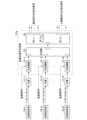
- FIG. 1 is a diagram illustrating an example of the configuration of a transmission directivity control device according to a first embodiment
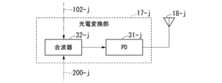
- 3A and 3B are diagrams illustrating an internal configuration of a photoelectric conversion unit according to the first embodiment and a connection relationship with an antenna element.
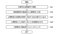
- 4 is a flowchart showing the operation of the transmission directivity control device according to the first embodiment.
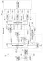
- FIG. 11 is a diagram illustrating an example of the configuration of a transmission directivity control device according to a second embodiment.
- FIG. 11 is a diagram showing an arrangement of antenna elements according to a second embodiment.
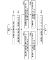
- 10 is a flowchart showing an operation of a transmission directivity control device according to a second embodiment.
- FIG. 13 is a diagram illustrating an example of the configuration of a transmission directivity control device according to a third embodiment.
- FIG. 13 is a diagram showing an internal configuration of a transmission optical signal generator according to a fourth embodiment, a connection relationship between the transmission optical signal generator and a light source, and a wavelength designation unit connected to the light source.
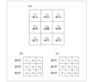
- FIG. 13A and 13B are diagrams showing the correspondence between wavelengths and directions according to the fourth embodiment, and the correspondence between output terminals assigned within a first scanning switching circuit and a second scanning switching circuit and wavelengths.
- FIG. 13 is a diagram illustrating an example of the configuration of a transmission directivity control device according to a fifth embodiment.
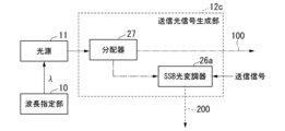
- FIG. 13 is a diagram (part 1) showing another configuration example of the transmission optical signal generating unit shown in the first, second, third, and fifth embodiments, the connection relationship with the light source, and a wavelength specifying unit connected to the light source.
- FIG. 2 is a diagram (part 2) showing another configuration example of the transmission optical signal generating unit shown in the first, second, third, and fifth embodiments, the connection relationship with the light source, and a wavelength specifying unit connected to the light source.
- 13A to 13C are diagrams illustrating other configuration examples of the photoelectric conversion unit shown in the first and fifth embodiments and the connection relationship with the antenna element.
- Fig. 1 is a block diagram showing an example of the configuration of a transmission directivity control device 1 according to a first embodiment.
- the transmission directivity control device 1 includes a wavelength designation unit 10, a light source 11, a transmission optical signal generation unit 12, a weighting unit 13, an operation unit 16, photoelectric conversion units 17-1 to 17-M, and antenna elements 18-1 to 18-M.
- M is a natural number of 2 or more, and in this description, a natural number is a positive integer not including 0.
- the wavelength specification unit 10 generates and outputs a wavelength specification signal including the wavelength ⁇ selected by the user in response to a user operation.
- the light source 11 is a wavelength-tunable light source, and generates and outputs CW (Continuous Wave) light of the wavelength ⁇ included in the wavelength specification signal received from the wavelength specification unit 10.
- the transmission optical signal generation unit 12 includes an optical modulator 21 and a splitter 22.
- the optical modulator 21 uses an externally applied electrical transmission signal as a baseband signal, and uses the baseband signal to intensity-modulate the light output by the light source 11 to generate a modulated optical signal.
- the splitter 22 splits the modulated optical signal generated by the optical modulator 21 into a carrier optical signal and an upper sideband optical signal.
- the splitter 22 outputs the split carrier optical signal to the optical path 100 connected to the splitter 22, and outputs the split upper sideband optical signal to the optical path 200.
- the optical paths 100 and 200 and the optical paths shown below are, for example, optical fibers. Note that in FIG. 1 and the figures shown below, the connecting lines shown by dashed and dotted lines indicate the optical paths along which the carrier optical signal is transmitted, and the connecting lines shown by dotted lines indicate the optical paths along which the upper sideband optical signal is transmitted.
- the operation unit 16 is capable of selecting a transmission direction, and outputs a switching instruction signal corresponding to the selected transmission direction.
- the weighting unit 13 includes a scanning switching circuit 14 and a scanning matrix circuit 15.
- the scanning switching circuit 14 is, for example, an optical switch, and includes one input terminal 14-S and M output terminals 14-E-1, 14-E-2, ..., 14-E-M.
- the input terminal 14-S is connected to an optical path 200.
- the scanning switching circuit 14 switches the input terminal 14-S to be connected to one of the output terminals 14-E-1 to 14-E-M according to the type of switching instruction signal output by the operation unit 16. In other words, there are M types of transmission directions that can be selected by the operation unit 16, and the operation unit 16 outputs a switching instruction signal corresponding to each of the M types of transmission directions.
- the scanning matrix circuit 15 is a circuit configured to impart a phase gradient using, for example, a delay line, a high dispersion line, a resonant ring, or the like, and may be, for example, a Butler matrix circuit or a Blass matrix circuit.
- the scanning matrix circuit 15 imparts a phase gradient to the supplied optical signal.
- the scanning matrix circuit 15 has M input terminals 15-S-1, 15-S-2, ..., 15-S-M and M output terminals 15-E-1, 15-E-2, ..., 15-E-M. Each of the M input terminals 15-S-1 to 15-S-M is connected to each of the output terminals 14-E-1 to 14-E-M of the scanning switching circuit 14.
- a phase inclination amount corresponding to the phase inclination to be applied is predetermined between each of the M input terminals 15-S-1 to 15-S-M and each of the M output terminals 15-E-1 to 15-E-M, and the circuit configuration is determined in advance so that the phase inclination amount is applied.
- "j" is any natural number between 1 and M.
- the scanning matrix circuit 15 When an optical signal is supplied from any one of the input terminals 15-S-j, the scanning matrix circuit 15 generates M optical signals by adding a tilt phase amount ⁇ j determined between the input terminal 15-S- j and each of the M output terminals 15-E-1 to 15-E-M to the supplied optical signal.
- the scanning matrix circuit 15 outputs each of the generated M optical signals from each of the M output terminals 15-E-1, 15-E-2, ..., 15-E-M.
- the unit of the tilt phase amount and other phase amounts when no unit is indicated is radian, which is a unit of the radian measure, and when indicated in the degree measure, the unit "°" is added.
- phase amounts of (0°, 30°, 60°) expressed in radians become the tilt phase amounts ⁇ j .
- 0° corresponds to the tilt phase amount ⁇ 1
- 30° corresponds to the tilt phase amount ⁇ 2
- 60° corresponds to the tilt phase amount ⁇ 3 , and thus a phase tilt that increases by 30° is added.
- phase amounts of (0°, 60°, 120°) expressed in radians become the tilt phase amounts ⁇ j .
- 0° corresponds to the tilt phase amount ⁇ 1
- 60° corresponds to the tilt phase amount ⁇ 2
- 120° corresponds to the tilt phase amount ⁇ 3 , and thus a phase tilt that increases by 60° is imparted.
- the subscript "j" in the tilt phase amount ⁇ j corresponds to the "j" indicating the position of the output terminal 15-E-j, and the tilt phase amount ⁇ j becomes a different phase amount when the input terminals 15-S-1 to 15-S-M are different.
- Each of the photoelectric conversion units 17-1 to 17-M is connected to each of the branch optical paths 102-1, 102-2, ..., 102-M that branch off from M branching points 101-1, 101-2, ..., 101-M in the optical path 100, and to the optical paths 200-1, 200-2, ..., 200-M that connect to each of the output terminals 15-E-1 to 15-E-M of the scanning matrix circuit 15.
- the branch optical paths 102-1 to 102-M are a part of the optical path 100, and the part of the optical path 100 other than the branch optical paths 102-1 to 102-M is called the main line of the optical path 100.
- Each of the photoelectric conversion units 17-1 to 17-M has the same internal configuration, and the photoelectric conversion unit 17-j has the internal configuration shown in FIG. 2.
- the photoelectric conversion unit 17-j has a photodiode (hereinafter referred to as PD (Photo Diode)) 31-j and a multiplexer 32-j.
- the multiplexer 32-j is connected to the branch optical path 102-j and the optical path 200-j.
- the multiplexer 32-j multiplexes the carrier optical signal supplied via the branch optical path 102-j and the upper sideband optical signal supplied via the optical path 200-j.
- the PD 31-j is connected to the multiplexer 32-j and the antenna element 18-j, and converts the optical signal output by the multiplexer 32-j into an electrical signal to generate an RF signal.
- the process by the photoelectric conversion unit 17-j to combine two optical signals, convert them into an electrical signal, and generate an RF signal is also referred to as photomixing.
- Antenna elements 18-1 to 18-M are arranged along an arrangement line that is arbitrarily determined in three-dimensional space, forming array antenna 19, which is a so-called one-dimensional array antenna.
- the arrangement line may be a straight line, or a curved line that forms a curved surface such as a concave or convex shape that is generally used as a two-dimensional array antenna.
- Each of antenna elements 18-1 to 18-M radiates an RF signal supplied from photoelectric conversion units 17-1 to 17-M connected to each of them as a radio wave.
- the radio waves radiated from each of antenna elements 18-1 to 18-M form a so-called transmission beam.
- the transmission beam radiated from antenna elements 18-1 to 18-M will be directed in any direction between the front direction 80 and the horizontal directions to the left and right on the plane of the paper surface of FIG. 1, such as the directions indicated by the symbols 81 and 82, or in the front direction 80, if the direction indicated by the symbol 80, which is the vertical upward direction on the paper surface of FIG. 1, is defined as the front direction 80.
- the direction of the transmission beam is determined by the phase tilt applied by the scanning matrix circuit 15.
- the direction of the transmission beam can be set to any direction between the front direction 80 and the left and right lateral directions.
- the phase tilt is fixedly determined in advance between each of the M input terminals 15-S-1 to 15-S-M and the M output terminals 15-E-1 to 15-E-M according to the direction of the arrangement line and the transmission direction desired by the user based on the direction of the arrangement line.
- the number of directions of the transmission beam when the phase tilt is fixedly determined is M, which is the number of input terminals 15-S-1 to 15-S-M of the scanning matrix circuit 15, i.e., the number of antenna elements 18-1 to 18-M.
- the photoelectric conversion units 17-1 to 17-M are arranged in a row along the arrangement line.
- the photoelectric conversion units 17-1 to 17-M are arranged so that the difference in path length of the optical path 100 from the output terminal to which the optical path 100 of the splitter 22 is connected to each of two adjacent photoelectric conversion units 17-1 to 17-M in the row (hereinafter referred to as path difference D) is constant, and this constant path difference D satisfies the connection condition (hereinafter referred to as the first connection condition) shown in the following formula (1).
- ⁇ is the wavelength ⁇ contained in the wavelength specification signal output by the wavelength specification unit 10, i.e., the wavelength ⁇ of the light generated and output by the light source 11.
- "a” is any natural number.
- the path difference D may be any value as long as it is a natural number multiple of the wavelength ⁇ of the light output by the light source 11.
- the optical path 100 is wired for the photoelectric conversion units 17-1 to 17-M as follows.
- the photoelectric conversion units 17-1 to 17-M are arranged in a row along the arrangement line at equal intervals with the length of the path difference D.
- the main line of the optical path 100 is wired along the row in which the photoelectric conversion units 17-1 to 17-M are lined up.
- the distance between adjacent branch points 101-1, 101-2, ..., 101-M is set to the length of the path difference D.
- Each of the branch points 101-1, 101-2, ..., 101-M is connected to each of the photoelectric conversion units 17-1 to 17-M by branch optical paths 102-1 to 102-M of the same length.
- the path difference D of the path length of the optical path 100 that starts at the output terminal to which the optical path 100 of the splitter 22 is connected and reaches each of the photoelectric conversion units 17-1 to 17-M appears as the difference in the path length of the optical path 100 that starts at the starting point and reaches each of the branch points 101-1 to 101-M.
- the phase of the carrier optical signal output by the splitter 22 when it reaches the photoelectric conversion unit 17-1 is set to "0" as a reference.
- the photoelectric conversion units 17-1 and 17-2 have a difference in the path length between the branching points 101-1 and 101-2, that is, a difference in the path difference D. Therefore, the optical signal output from the splitter 22 and arriving at the photoelectric conversion unit 17-2 rotates in phase due to the path difference D between the branching points 101-1 and 101-2, and the phase advances by an amount corresponding to the length of the path difference D.
- the optical signal output from the splitter 22 and arriving at the photoelectric conversion unit 17-2 is an optical signal with a phase advance of "2a ⁇ " compared to the optical signal output from the splitter 22 and arriving at the photoelectric conversion unit 17-1.
- the adjacent branching points 101-1, 101-2, ..., 101-M are spaced equally apart, so the optical signal output from the splitter 22 and reaching the photoelectric conversion unit 17-j is a signal with a phase lead of "2(j-1)a ⁇ " compared to the optical signal output from the splitter 22 and reaching the photoelectric conversion unit 17-1.
- the optical paths 200-1 to 200-M output from the output terminals 15-E-1 to 15-E-M of the scanning matrix circuit 15 and reaching the photoelectric conversion units 17-1 to 17-M are wired so as not to have any path difference. Therefore, the difference in phase between the upper sideband optical signals output from the output terminals 15-E-1 to 15-E-M of the scanning matrix circuit 15 and reaching the photoelectric conversion units 17-1 to 17-M is due to the amount of tilt phase ⁇ j provided by the scanning matrix circuit 15.
- the processing by the transmission directivity control device 1 will be described with reference to Fig. 3.
- the user of the transmission directivity control device 1 determines the wavelength ⁇ , and wires the optical paths 100 to the photoelectric conversion units 17-1 to 17-M so that the path difference D is in accordance with the determined wavelength ⁇ and the first connection condition.
- the wavelength designation unit 10 outputs a wavelength designation signal including the wavelength ⁇ to the light source 11 in response to the operation.
- the user operates the operation unit 16 to select the desired transmission direction, and in response to this operation, the operation unit 16 outputs a switching instruction signal corresponding to the selected transmission direction to the scanning switching circuit 14.
- the scanning switching circuit 14 connects, for example, the input terminal 14-S to the output terminal 14-E-j, which is one of the output terminals 14-E-1 to 14-E-M.
- the process of the flowchart shown in FIG. 3 is started.
- the light source 11 takes in the wavelength designation signal output by the wavelength designation unit 10.
- the light source 11 generates light of wavelength ⁇ included in the taken in wavelength designation signal, and outputs the generated light to the optical modulator 21.
- the optical modulator 21 generates a modulated optical signal by intensity modulating the light using an externally applied transmission signal.
- the optical modulator 21 outputs the generated modulated optical signal to the splitter 22 (Sa1).
- the splitter 22 splits the modulated optical signal output by the optical modulator 21 into a carrier optical signal and an upper sideband optical signal.
- the carrier optical signal is expressed by the following equation (2)
- the upper sideband optical signal is expressed by the following equation (3).
- ⁇ C is the angular frequency of the light generated by the light source 11, and t is time.
- ⁇ RF is the angular frequency of the RF signal, and corresponds to the frequency difference between the carrier optical signal and the upper sideband optical signal.
- the demultiplexer 22 outputs the carrier optical signal to the optical path 100, and outputs the upper sideband optical signal to the optical path 200 (Sa2).
- the scanning switching circuit 14 receives the upper sideband optical signal output by the splitter 22 from the input terminal 14-S and outputs it from the output terminal 14-E-j (Sa3).
- the scanning matrix circuit 15 receives the upper sideband optical signal output from the output terminal 14-E-j of the scanning switching circuit 14 from the input terminal 15-S-j.
- the scanning matrix circuit 15 generates M upper sideband optical signals by applying a tilt phase amount ⁇ j determined between the input terminal 15-S-j and each of the M output terminals 15-E-1 to 15-E-M to the received upper sideband optical signal.
- the upper sideband optical signal output from the output terminal 15-E-j of the scanning matrix circuit 15 is expressed by the following equation (4).
- the scanning matrix circuit 15 outputs the generated M upper sideband optical signals from each of the M output terminals 15-E-1 to 15-E-M (Sa4).
- Each of the photoelectric conversion units 17-1 to 17-M is supplied with a carrier optical signal from the splitter 22 via the optical path 100, and with an upper sideband optical signal via the optical paths 200-1 to 200-M.
- a carrier optical signal from the splitter 22 via the optical path 100
- an upper sideband optical signal via the optical paths 200-1 to 200-M.
- the carrier optical signal supplied to the multiplexer 32-j of the photoelectric conversion unit 17-j via the branch optical path 102-j has a phase lead of "2(j-1)a ⁇ " as described above, and is therefore expressed by the following equation (5).
- multiplexer 32-j multiplexes the carrier optical signal expressed by formula (5) and the upper sideband optical signal expressed by formula (4) to generate a multiplexed optical signal and outputs it to PD 32-j.
- the multiplexed optical signal generated by multiplexer 32-j is expressed by the following formula (6).
- PD32-j When PD32-j takes in the combined optical signal output by multiplexer 32-j, it converts the combined optical signal into an electrical signal. When converting to an electrical signal, PD32-j performs square-law detection on the combined optical signal, and generates an electrical signal of a specific RF frequency band component that depends on the output frequency characteristics of PD32-j from the result of this square-law detection.
- the square-law detection by PD32-j can be expressed as the right-hand side of the following equation (7).
- the RF signal output by PD 32-j becomes an RF signal v RF_j expressed by the following equation (8) in which the RF frequency band is extracted from the calculation result of the right side of equation (7).
- the RF signal v RF_j becomes a signal proportional to cos( ⁇ RF t- ⁇ j +2ja ⁇ -2a ⁇ ).
- Each of the photoelectric conversion units 17-1 to 17-M outputs the generated RF signal to the antenna elements 18-1 to 18-M connected to each of them.
- Each of the antenna elements 18-1 to 18-M radiates the RF signal output by the photoelectric conversion unit 17-1 to 17-M connected to each of them as a radio wave (Sa5), and the process ends.
- the phase difference between the RF signals output by photoelectric conversion unit 17-(j+1) and photoelectric conversion unit 17-j is "- ⁇ j+1 + ⁇ j + 2a ⁇ ".
- "2a ⁇ ” is "a” times 2 ⁇ , where "a” is a natural number. Therefore, the phase indicated by this phase difference coincides with "- ⁇ j+1 + ⁇ j ", and therefore the phase difference "2a ⁇ ” occurring in the carrier optical signal supplied to each of photoelectric conversion units 17-1 to 17-M is absorbed by the path difference D of optical path 100 until the carrier optical signal reaches each of photoelectric conversion units 17-1 to 17-M.
- the user operates the wavelength specification unit 10 to select the wavelength ⁇ of the light generated by the light source 11.
- the optical path 100 is wired to the photoelectric conversion units 17-1 to 17-M so as to satisfy the first connection condition in advance.
- the path difference D is determined in advance, and the optical path 100 is wired to the photoelectric conversion units 17-1 to 17-M.
- the wavelength ⁇ may be determined so as to satisfy the formula (1), and the determined wavelength ⁇ may be selected by the user in the wavelength specification unit 10.
- the path difference D and the wavelength ⁇ of the light generated by the light source 11 are selected so that the phase difference occurring in the carrier optical signal supplied to each of the photoelectric conversion units 17-1 to 17-M is absorbed by the path difference D of the optical path 100 until the carrier optical signal reaches each of the photoelectric conversion units 17-1 to 17-M.
- the phase difference of the RF signals output by the adjacent photoelectric conversion unit 17-(j+1) and photoelectric conversion unit 17-j becomes "- ⁇ j+1 + ⁇ j ".
- the phase difference of this RF signal indicates the phase tilt imparted by the scanning matrix circuit 15, so by using these RF signals, it is possible to propagate the radio waves of the RF signals radiated from the antenna elements 18-1 to 18-M in the transmission direction desired by the user.
- the circuit scale required to make the optical paths the same path length becomes enormous as the number of antenna elements 18-1 to 18-M, 18-1-1 to 18-3-3, i.e., the number of photoelectric conversion units 17-1 to 17-M, 17-1-1 to 17-3-3, increases.
- the wiring of the optical path 100 to the photoelectric conversion units 17-1 to 17-M is a simple configuration in which one optical path 100 is branched into M and connected to each of the photoelectric conversion units 17-1 to 17-M, thereby achieving the above-mentioned objective.
- the phase shift of the optical signal is performed by an analog circuit. Therefore, compared to a fully digitally controlled array antenna in which phase shifting is performed entirely by digital signal processing, the number of analog-digital converters can be significantly reduced.
- the transmission directivity control device 1 of the first embodiment even if the scale of the array antenna 19 is large, it is possible to control the transmission directivity by a circuit with a simple structure suitable for miniaturization and mass production, making it possible to perform appropriate weighting without complicating the wiring structure.
- Second Embodiment 4 is a block diagram showing a configuration example of a transmission directivity control device 1a according to the second embodiment.
- the transmission directivity control device 1a includes a wavelength designation unit 10, a light source 11, a transmission optical signal generation unit 12, a weighting unit 13a, an operation unit 16a, photoelectric conversion units 17-1-1 to 17-3-3, and antenna elements 18-1-1 to 18-3-3.
- the antenna elements 18-1-1 to 18-3-3 are arranged along a first arrangement line that is arbitrarily determined in a three-dimensional space and a second arrangement line that intersects with the first arrangement line.
- the first arrangement line and the second arrangement line may be straight lines, or may be curved lines that form a curved surface such as a concave or convex shape that is generally used as a two-dimensional array antenna.
- the first arrangement line and the second arrangement line are straight lines that are orthogonal to each other, the direction of the first arrangement line is the vertical direction in the three-dimensional space, and the second arrangement line is the horizontal direction in the three-dimensional space.
- the antenna elements 18-1-1 to 18-3-3 are arranged, for example, as shown in FIG.
- Each of the photoelectric conversion units 17-1-1 to 17-3-3 is connected to each of the antenna elements 18-1-1 to 18-3-3, and is arranged in a matrix shape such that the row direction coincides with the direction of the first arrangement line, and the column direction coincides with the direction of the second arrangement line.
- "i" is any natural number between 1 and 3 indicating the row position
- "j" is any natural number between 1 and 3 indicating the column position.
- the photoelectric conversion unit 17-i-j arranged in the i-th row and j-th column includes a multiplexer and a PD, similar to the photoelectric conversion unit 17-j of the first embodiment shown in FIG. 2, and performs photomixing on two supplied optical signals.
- the multiplexer and PD included in the photoelectric conversion unit 17-i-j are referred to as multiplexer 32-i-j and PD 31-i-j, respectively.
- the weighting unit 13a includes a first scanning switching circuit 14A, a second scanning switching circuit 14B, a first scanning matrix circuit 15A, and a second scanning matrix circuit 15B.
- the second scanning matrix circuit 15B is determined to have a phase tilt according to the direction of the second arrangement line and the transmission direction desired by the user based on the direction of the second arrangement line.
- the tilt phase amount determined in advance between each of the input terminals 15A-S-1 to 15A-S-3 and each of the output terminals 15A-E-1 to 15A-E-3 is represented as ⁇ Vi , which is ⁇ with "Vi" added.
- the tilt phase amount ⁇ V1 is the tilt phase amount imparted to the optical signal output from the output terminal 15A-E-1
- the tilt phase amount ⁇ V2 is the tilt phase amount imparted to the optical signal output from the output terminal 15A-E-2
- the tilt phase amount ⁇ V3 is the tilt phase amount imparted to the optical signal output from the output terminal 15A-E-3.
- the values of ( ⁇ V1 , ⁇ V2 , ⁇ V3 ) are different depending on which of the input terminals 15A-S-1, 15A-S-2, and 15A-S-3 the optical signal is supplied to.
- the tilt phase amount determined in advance between each of the input terminals 15B-S-1 to 15B-S-3 and each of the output terminals 15B-E-1 to 15B-E-3 is represented as ⁇ Hj , which is ⁇ with "Hj" added.
- the tilt phase amount ⁇ H1 is the tilt phase amount imparted to the optical signal output from the output terminal 15B-E-1
- the tilt phase amount ⁇ H2 is the tilt phase amount imparted to the optical signal output from the output terminal 15B-E-2
- the tilt phase amount ⁇ H3 is the tilt phase amount imparted to the optical signal output from the output terminal 15B-E-3.
- the values of ( ⁇ H1 , ⁇ H2 , ⁇ H3 ) are different depending on which of the input terminals 15B-S-1, 15B-S-2, and 15B-S-3 the optical signal is supplied to.
- connection conditions (hereinafter referred to as second connection conditions) between the first scanning matrix circuit 15A, the second scanning matrix circuit 15B, and each of the photoelectric conversion units 17-1-1 to 17-3-3 are shown by the connection relationships shown below.
- connection relationship of the optical path 100-1 between the output terminal 15A-E-1 of the first scanning matrix circuit 15A and each of the photoelectric conversion units 17-1-1, 17-1-2, and 17-1-3 in the first row is the same as the connection relationship of the optical path 100 between the output terminal to which the optical path 100 of the demultiplexer 22 in the first embodiment is connected and each of the photoelectric conversion units 17-1, 17-2, and 17-3.
- the path difference D in the first embodiment is represented as a path difference D2 in the second embodiment. Therefore, the path difference D2 is expressed as the following equation (10).
- connection relationship of the optical path 100-2 between the output terminal 15A-E-2 and each of the photoelectric conversion units 17-2-1, 17-2-2, and 17-2-3 in the second row, and the connection relationship of the optical path 100-3 between the output terminal 15A-E-3 and each of the photoelectric conversion units 17-3-1, 17-3-2, and 17-3-3 in the third row are the same as the connection relationship of the optical path 100-1 between the output terminal 15A-E-1 and each of the photoelectric conversion units 17-1-1, 17-1-2, and 17-1-3 in the first row.
- connection relationship of the optical path 200-1 between the output terminal 15B-E-1 of the second scanning matrix circuit 15B and each of the photoelectric conversion units 17-1-1, 17-2-1, and 17-3-1 in the first column is the same as the connection relationship of the optical path 100-1 between the output terminal 15A-E-1 and each of the photoelectric conversion units 17-1-1, 17-1-2, and 17-1-3 in the first row, but differs in that the path difference is not path difference D2 but path difference D1 shown in the following equation (11).
- connection relationship of the optical path 200-2 between the output terminal 15B-E-2 and each of the photoelectric conversion units 17-1-2, 17-2-2, and 17-3-2 in the second row, and the connection relationship of the optical path 200-3 between the output terminal 15B-E-3 and each of the photoelectric conversion units 17-1-3, 17-2-3, and 17-3-3 in the third row are the same as the connection relationship of the optical path 200-1 between the output terminal 15B-E-1 and each of the photoelectric conversion units 17-1-1, 17-2-1, and 17-3-1 in the first row.
- the second connection condition can be said to be a condition including the column direction condition and row direction condition shown below. That is, the column direction condition is a condition in which the path difference D2 of the optical paths 100-1 to 100-3 starting from each of the output terminals 15A-E-1, 15A-E- 2 , and 15A-E-3 of the first scanning matrix circuit 15A until each of the two adjacent photoelectric conversion units 17-1-1 to 17-3-3 in the corresponding row of the photoelectric conversion units 17-1-1 to 17-3-3 is constant, and this path difference D2 is a value of any natural number a times the wavelength ⁇ of the light generated by the light source 11, as shown in formula (10).
- the row direction condition is a condition in which a path difference D1 of the optical paths 200-1 to 200-3 starting from each of the output terminals 15B-E-1, 15B-E-2, 15B-E-3 of the second scanning matrix circuit 15B and reaching each of two adjacent photoelectric conversion units 17-1-1 to 17-3-3 in the corresponding column of photoelectric conversion units 17-1-1 to 17-3-3 is constant, and this path difference D1 is a value of any natural number b times the wavelength ⁇ of the light generated by the light source 11, as shown in equation (11).
- optical paths 100-1 to 100-3, 200-1 to 200-3 are wired to photoelectric conversion units 17-1-1 to 17-3-3 as follows: In the combination of photoelectric conversion units 17-1-1, 17-1-2, and 17-1-3 in the first row, the combination of photoelectric conversion units 17-2-1, 17-2-2, and 17-2-3 in the second row, and the combination of photoelectric conversion units 17-3-1, 17-3-2, and 17-3-3 in the third row, they are all arranged so that the adjacent intervals in the column direction, i.e., the second arrangement line direction, are all path differences D2 .
- the combination of photoelectric conversion units 17-1-1, 17-2-1, and 17-3-1 in the first column, the combination of photoelectric conversion units 17-1-2, 17-2-2, and 17-3-2 in the second column, and the combination of photoelectric conversion units 17-1-3, 17-2-3, and 17-3-3 in the third column they are all arranged so that the adjacent spacing in the row direction, i.e., the first arrangement line direction, is all path difference D1 .
- the optical paths 100-1 to 100-3 connected to the output terminals 15A-E-1 to 15A-E-3 of the first scanning matrix circuit 15A are wired along the column direction, as in the first embodiment.
- the branch points are determined so that the interval between adjacent branch points on the main lines of the optical paths 100-1 to 100-3 matches the interval in the column direction of the photoelectric conversion units 17-1-1 to 17-3-3, i.e., the path difference D 2.
- Each branch point of the optical path 100-1 is connected to each of the photoelectric conversion units 17-1-1, 17-1-2, and 17-1-3 in the first row by branch optical paths of the same length.
- the optical paths 100-2 and 100-3 are connected to the photoelectric conversion units 17-2-1, 17-2-2, and 17-2-3 in the second row and the photoelectric conversion units 17-3-1, 17-3-2, and 17-3-3 in the third row, respectively.
- the optical paths 200-1 to 200-3 connected to the output terminals 15B-E-1 to 15B-E-3 of the second scanning matrix circuit 15B are wired along the row direction.
- the branch points are determined so that the interval between adjacent branch points on the main line of each of the optical paths 200-1 to 200-3 matches the interval in the row direction between the photoelectric conversion units 17-1-1 to 17-3-3, i.e., the path difference D 1.
- Each branch point of the optical path 200-1 is connected to each of the photoelectric conversion units 17-1-1, 17-2-1, and 17-3-1 in the first column by branch optical paths of the same length.
- the optical paths 200-2 and 200-3 respectively connect the photoelectric conversion units 17-1-2, 17-2-2, and 17-3-2 in the second column to the photoelectric conversion units 17-1-3, 17-2-3, and 17-3-3 in the third column.
- a path difference D 2 appears in the length between the adjacent branch points 101-3-1 and 101-3-2 in the optical path 100-3 and the length between the branch points 101-3-2 and 101-3-3. This is similar to the other optical paths 100-1 and 100-2.
- a path difference D 1 appears in the length between the adjacent branch points 201-1-1 and 201-1-2 in the optical path 200-1 and the length between the branch points 201-1-2 and 201-1-3. This is similar to the other optical paths 200-2 and 200-3.
- the process performed by the transmission directivity control device 1a of the second embodiment will be described with reference to Fig. 6.
- the user of the transmission directivity control device 1a determines the wavelength ⁇ , and wires the optical paths 100-1 to 100-3, 200-1 to 200-3 to the photoelectric conversion units 17-1-1 to 17-3-3 so that the path differences D1 , D2 are in accordance with the determined wavelength ⁇ and the second connection condition.
- the wavelength designation unit 10 outputs a wavelength designation signal including the wavelength ⁇ to the light source 11 in response to the operation.
- the user operates the operation unit 16a to select the desired transmission direction, and in response to this operation, the operation unit 16a outputs a switching instruction signal corresponding to the selected transmission direction to the first scanning switching circuit 14A and the second scanning switching circuit 14B.
- the first scanning switching circuit 14A that receives this switching instruction signal connects, for example, the input terminal 14A-S to output terminal 14A-E-i, which is one of the output terminals 14A-E-1 to 14A-E-3.
- the second scanning switching circuit 14B that receives this switching instruction signal connects, for example, the input terminal 14B-S to output terminal 14B-E-j, which is one of the output terminals 14B-E-1 to 14B-E-3.
- the processes Sb1 and Sb2 are the same as the processes Sa1 and Sa2 in the first embodiment shown in FIG. 3, and are performed by the light source 11 and the transmission optical signal generation unit 12.
- the first scanning switching circuit 14A takes in the carrier optical signal output by the splitter 22 from the input terminal 14A-S and outputs it from the output terminal 14A-E-i (Sb3-1).
- the first scanning matrix circuit 15A takes in the carrier optical signal output from the output terminal 14A-E-i of the first scanning switching circuit 14A from the input terminal 15A-S-i.
- the first scanning matrix circuit 15A gives the taken-in carrier optical signal a tilt phase amount ⁇ Vi determined between the input terminal 15A-S-i and each of the output terminals 15A-E-1 to 15A-E-3 to generate three carrier optical signals. Since the carrier optical signal output by the splitter 22 is expressed by equation (2), the carrier optical signal output from the output terminal 15A-E-i of the first scanning matrix circuit 15A is expressed by the following equation (12).
- the first scanning matrix circuit 15A outputs the generated optical signals of the three carrier waves from each of the output terminals 15A-E-1 to 15A-E-3 (Sb4-1).
- the processing of Sb3-2 and Sb4-2 is the same as the processing of Sa3 and Sa4 in the first embodiment shown in FIG. 3 except that M is set to 3 and the tilt phase amount applied by the scanning matrix circuit 15 is replaced by ⁇ Hj from ⁇ j , and the processing performed by the scanning switching circuit 14 is performed by the second scanning switching circuit 14B, and the processing performed by the scanning matrix circuit 15 is performed by the second scanning matrix circuit 15B.
- the upper sideband optical signal output by the splitter 22 is expressed by equation (3), so in the processing of Sb4-2, the upper sideband optical signal output from the output terminal 15B-E-j of the second scanning matrix circuit 15B is expressed by the following equation (13).
- the carrier optical signal that reaches the jth column photoelectric conversion unit 17-i-j has a phase lead of "2(j-1)a ⁇ ", and is expressed by the following equation (14).
- the upper sideband optical signal that reaches the photoelectric conversion unit 17-i-j in the i-th row has a phase lead of "2(i-1)b ⁇ ", and is expressed by the following equation (15).
- the photoelectric conversion unit 17-i-j photomixes the carrier optical signal shown in equation (14) with the upper sideband optical signal shown in equation (15). That is, the multiplexer 32-i-j included in the photoelectric conversion unit 17-i-j multiplexes the carrier optical signal shown in equation (14) with the upper sideband optical signal shown in equation (15) to generate a multiplexed optical signal.
- the PD 31-i-j converts the multiplexed optical signal generated by the multiplexer 32-i-j into an electrical signal.
- the PD 32-i-j When converting to an electrical signal, the PD 32-i-j performs square-law detection on the multiplexed optical signal, and generates an electrical signal of a predetermined RF frequency band component that depends on the output frequency characteristics of the PD 32-i-j from the result of the square-law detection.
- the square-law detection by the PD 32-i-j can be expressed as the right side of the following equation (16).
- the RF signal output from the photoelectric conversion unit 17-i-j becomes an RF signal v RF_ij expressed by the following equation (17), which is obtained by extracting the RF frequency band from the calculation result of the right side of equation (16).
- the RF signal v RF_ij becomes a signal proportional to cos( ⁇ RF t+( ⁇ Vi - ⁇ Hj )+2(j-1)a ⁇ +2(i-1)b ⁇ ).
- Each of the photoelectric conversion units 17-1-1 to 17-3-3 outputs the generated RF signal to the antenna elements 18-1-1 to 18-3-3 connected to each of them.
- Each of the antenna elements 18-1-1 to 18-3-3 radiates the RF signal output by the photoelectric conversion units 17-1-1 to 17-3-3 connected to each of them as a radio wave (Sb5), and the process ends.
- the RF signal output by the photoelectric conversion unit 17-i-(j+1) adjacent to the photoelectric conversion unit 17-i-j in the column direction is the signal shown in the following equation (19) by substituting "j+1" for "j" on the right-hand side of equation (17).
- the phase difference between the RF signals output by the photoelectric conversion unit 17-(i+1)-j and the photoelectric conversion unit 17-i-j is " ⁇ V(i+1) - ⁇ Vi +2b ⁇ ".
- "2b ⁇ ” is "b" times 2 ⁇ , where "b” is a natural number. Therefore, the phase indicated by the phase difference coincides with " ⁇ V(i+1) - ⁇ Vi ", so the phase difference "2b ⁇ ” occurring in the upper sideband optical signal supplied to each of the photoelectric conversion units 17-1-1 to 17-3-3 is absorbed by the path difference D1 of the optical paths 200-1 to 200-3 until the upper sideband optical signal reaches each of the photoelectric conversion units 17-1-1 to 17-3-3 for each row.
- the phase difference between the RF signals output by the photoelectric conversion unit 17-i-(j+1) and the photoelectric conversion unit 17-i-j is "- ⁇ H(i+1) + ⁇ Hi +2a ⁇ ".
- "2a ⁇ ” is "a" times 2 ⁇ , where "a” is a natural number. Therefore, the phase indicated by the phase difference coincides with "- ⁇ H(i+1) + ⁇ Hi ", so the phase difference "2a ⁇ ” occurring in the carrier optical signal supplied to each of the photoelectric conversion units 17-1-1 to 17-3-3 is absorbed by the path difference D2 of the optical paths 100-1 to 100-3 until the carrier optical signal reaches each of the photoelectric conversion units 17-1-1 to 17-3-3 for each column.
- the user operates the wavelength designation unit 10 to select the wavelength ⁇ of the light generated by the light source 11.
- the optical paths 100-1 to 100-3 and 200-1 to 200-2 are wired to the photoelectric conversion units 17-1-1 to 17-3-3 so as to satisfy the second connection condition in advance.
- the path difference D 1 and the path difference D 2 are determined in advance, and the optical paths 100-1 to 100-3 and 200-1 to 200-2 are wired to the photoelectric conversion units 17-1-1 to 17-3-3.
- the wavelength ⁇ may be determined so as to satisfy the formulas (10) and (11), and the determined wavelength ⁇ may be selected by the user in the wavelength designation unit 10.
- the path difference D2, the path difference D1, and the wavelength ⁇ generated by the light source 11 are selected so that the path difference D2 of the optical paths 100-1 to 100-3 until the optical signal of the carrier wave with a phase tilt reaches each of the photoelectric conversion units 17-1-1 to 17-3-3 in the column direction absorbs the phase difference occurring in the optical signal of the carrier wave with a phase tilt that is supplied to each of the photoelectric conversion units 17-1-1 to 17-3-3, and so that the path difference D1 of the optical paths 200-1 to 200-3 until the optical signal of the upper sideband wave with a phase tilt reaches each of the photoelectric conversion units 17-1-1 to 17-3-3 in the row direction absorbs the phase difference occurring in the optical signal of the upper sideband wave with a phase tilt that is supplied to each of the photoelectric conversion units 17-1-1 to 17-3-3.
- the phase difference between the RF signals output by the photoelectric conversion unit 17-(i+1)-j and the photoelectric conversion unit 17-i-j adjacent in the row direction is " ⁇ V(i+1) - ⁇ Vi "
- the phase difference between the RF signals output by the photoelectric conversion unit 17-i-(j+1) and the photoelectric conversion unit 17-i-j adjacent in the column direction is "- ⁇ H(i+1) + ⁇ Hi ".
- the former phase difference " ⁇ V(i+1) - ⁇ Vi " indicates the phase inclination given by the first scanning matrix circuit 15A
- the latter "- ⁇ H(i+1) + ⁇ Hi " indicates the phase inclination given by the second scanning matrix circuit 15B. Therefore, by using these RF signals, it is possible to propagate the radio waves of the RF signals radiated from the antenna elements 18-1-1 to 18-3-3 in the transmission direction desired by the user.
- the transmission directivity control device 1a of the second embodiment has the following effects in addition to the effects of the transmission directivity control device 1 of the first embodiment described above. That is, when scanning a two-dimensional transmission beam, the transmission directivity control device 1a can perform large-scale, two-dimensional transmission beam scanning while significantly suppressing an increase in the number of components in the circuit that forms the transmission beam and the complexity of the structure, such as three-dimensional intersections and three-dimensional wiring, when scanning a two-dimensional transmission beam. In other words, by using the transmission directivity control device 1a, even if the scale of the array antenna 19a is large, it is possible to perform appropriate weighting without complicating the wiring structure, and it is possible to control the transmission directivity using a circuit with a simple structure suitable for miniaturization and mass production.
- N and M are natural numbers, and one of N and M is at least a natural number equal to or greater than 2.
- Third Embodiment Fig. 7 is a block diagram showing a configuration example of a transmission directivity control device 1b according to the third embodiment.
- the transmission directivity control device 1b includes a wavelength designation unit 10, a light source 11, a transmission optical signal generation unit 12, a weighting unit 13b, an operation unit 16a, photoelectric conversion units 17-1-1 to 17-3-3, and antenna elements 18-1-1 to 18-3-3.
- the weighting unit 13b includes a first scanning switching circuit 14A, a second scanning switching circuit 14B, multiplexers 41-1 to 41-3, splitters 42-1 to 42-3, and a scanning matrix circuit 15C.
- the multiplexers 41-1 to 41-3 multiplex the supplied carrier optical signal and the upper sideband optical signal to generate a multiplexed optical signal.
- the input side of the multiplexer 41-1 is connected to the output terminal 14A-E-1 of the first scanning switching circuit 14A and the output terminal 14B-E-1 of the second scanning switching circuit 14B, and the output side is connected to the input terminal 15C-S-1 of the scanning matrix circuit 15C.
- the input side of the multiplexer 41-2 is connected to the output terminal 14A-E-2 of the first scanning switching circuit 14A and the output terminal 14B-E-2 of the second scanning switching circuit 14B, and the output side is connected to the input terminal 15C-S-2 of the scanning matrix circuit 15C.
- the multiplexer 41-3 is connected on the input side to the output terminal 14A-E-3 of the first scanning switching circuit 14A and the output terminal 14B-E-3 of the second scanning switching circuit 14B, and on the output side to the input terminal 15C-S-3 of the scanning matrix circuit 15C.
- the splitters 42-1 to 42-3 split the supplied optical signal into a carrier optical signal and an upper sideband optical signal.
- the splitter 42-1 is connected to the output terminal 15C-E-1 of the scanning matrix circuit 15C on the input side, and to the optical paths 100-1 and 200-1 on the output side.
- the splitter 42-2 is connected to the output terminal 15C-E-2 of the scanning matrix circuit 15C on the input side, and to the optical paths 100-2 and 200-2 on the output side.
- the splitter 42-3 is connected to the output terminal 15C-E-3 of the scanning matrix circuit 15C on the input side, and to the optical paths 100-3 and 200-3 on the output side.
- the connection relationship between each of the optical paths 100-1 to 100-3 and 200-1 to 200-3 and each of the photoelectric conversion units 17-1-1 to 17-3-3 is the same as in the second embodiment.
- the scanning matrix circuit 15C also serves as the first scanning matrix circuit 15A and the second scanning matrix circuit 15B in the transmission directivity control device 1a of the second embodiment. Therefore, in the process shown in Fig. 6, after the processes Sb3-1 and Sb3-2, a process is added in which the carrier optical signal and the upper sideband optical signal are multiplexed by the multiplexers 41-1 to 41-3, and the processes Sb4-1 and Sb4-2 are performed by the scanning matrix circuit 15C.
- the amount of tilt phase imparted by the first scanning matrix circuit 15A is represented by ⁇ Vi , but more specifically, the amount of tilt phase imparted to an optical signal output from an output terminal 15A-E-i when an optical signal is supplied to an input terminal 15A-S-p can be represented as ⁇ Vpi .
- the amount of tilt phase imparted by the second scanning matrix circuit 15B is represented by ⁇ Hj , but more specifically, the amount of tilt phase imparted to an optical signal output from an output terminal 15B-E-j when an optical signal is supplied to an input terminal 15B-S-p can be represented as ⁇ Hpj .
- p, i, j, and q shown below are any natural numbers between 1 and 3.
- the first scanning matrix circuit 15A and the second scanning matrix circuit 15B are different circuits, so the tilt phase amount ⁇ Vpq and the tilt phase amount ⁇ Hpq can be different values.
- the transmission beam when viewed from the direction in which the main body of the transmission directivity control device 1a indicated by reference numeral 90 exists, the transmission beam can be transmitted in a total of nine directions, combining three directions: a direction parallel to the horizontal plane, i.e., a direction with an inclination of 0° with respect to the horizontal plane, a direction inclined by ⁇ ° upward from the horizontal plane, and a direction inclined by ⁇ ° downward from the horizontal plane; a direction parallel to the vertical plane, i.e., a direction with an inclination of 0° with respect to the vertical plane, a direction inclined by ⁇ ° to the right from the vertical plane, and a direction inclined by ⁇ ° to the left from the horizontal plane.
- ⁇ Vpq ⁇ ⁇ Hpq can be satisfied, so that ⁇ ° and ⁇ ° can be different angles.
- ⁇ Vpq ⁇ Hpq , so ⁇ ° and ⁇ ° are the same.
- each of the splitters 42-1 to 42-3 takes in the optical signals output from the output terminals 15C-E-1 to 15C-E-3 connected to it, and splits them into a carrier optical signal and an upper sideband optical signal.
- Each of the splitters 42-1 to 42-3 outputs the split carrier optical signal to the optical paths 100-1 to 100-3 connected to it, and outputs the split upper sideband optical signal to the optical paths 200-1 to 200-3 connected to it.
- the process of Sb5 is performed, and the process ends.
- the transmission directivity control device 1b of the third embodiment has the following effects in addition to the effects of the transmission directivity control device 1a of the second embodiment described above.
- the transmission directivity control device 1a of the second embodiment requires two matrix circuits, the first scanning matrix circuit 15A and the second scanning matrix circuit 15B, but the transmission directivity control device 1b of the third embodiment has a single matrix circuit, the scanning matrix circuit 15C, that applies a phase gradient. Therefore, the transmission directivity control device 1b can be made smaller than the transmission directivity control device 1a.
- the range of directions of a transmission beam that can be transmitted by the transmission directivity control device 1b is limited.
- the transmission directivity control device 1a can arrange any number of antenna elements 18-i-j in each of the first arrangement line direction and the second arrangement line direction
- the configuration of the array antenna 19a can be other than 3 x 3, but the number of antenna elements 18-i-j that can be arranged in the first arrangement line direction and the second arrangement line direction must be the same.
- the first scanning matrix circuit 15A and the second scanning matrix circuit 15B weight the antenna elements 18-1-1 to 18-3-3 arranged along the first arrangement line and the antenna elements 18-1-1 to 18-3-3 arranged along the second arrangement line, and electronically perform beam steering.
- the number of elements in the weighting section is proportional to the square of the number of antenna elements.
- the transmission directivity control device 1a of the second embodiment can suppress an increase in the number of elements in the weighting section 13a that occurs with an increase in the number of antenna elements, compared to a general configuration.
- the scanning matrix circuit 15C serves both the roles of the first scanning matrix circuit 15A and the second scanning matrix circuit 15B, so that the transmission directivity control device 1b can suppress an increase in the number of elements in the weighting section 13b that occurs with an increase in the number of antenna elements more than the transmission directivity control device 1a of the second embodiment.
- the transmission directivity control device 1a of the second embodiment described above has one light source 11 and has a single-beam configuration in which one transmission beam is transmitted from light of one wavelength ⁇ .
- the transmission directivity control device 1a by configuring the transmission directivity control device 1a as follows, it is possible to configure it as a multi-beam configuration in which multiple transmission beams are transmitted in parallel.
- the light source 11 is replaced with nine light sources 11-1, 11-2, ..., 11-9 having the same configuration as the light source 11.
- the wavelength designation unit 10 is replaced with nine wavelength designation units 10-1, 10-2, ..., 10-9 having the same configuration as the wavelength designation unit 10.
- Each of the wavelength designation units 10-1 to 10-9 is connected to each of the light sources 11-1 to 11-9, and outputs a wavelength designation signal including each of the wavelengths ⁇ 1 to ⁇ 9 corresponding to each of the light sources 11-1 to 11-9 and selected by a user, to each of the light sources 11-1 to 11-9 .
- the transmission optical signal generating unit 12 is replaced with the transmission optical signal generating unit 12a shown in FIG. 8.
- the transmission optical signal generating unit 12a includes nine optical modulators 21-1, 21-2, ..., 21-9, a multiplexer 23, and an optical comb filter 24.
- Each of the optical modulators 21-1 to 21-9 has the same configuration as the optical modulator 21.
- Each of the optical modulators 21-1 to 21-9 is connected to each of the light sources 11-1 to 11-9, and intensity-modulates the light generated and output by the light sources 11-1 to 11-9 connected to each of them with a different transmission signal 1, transmission signal 2, ..., transmission signal 9 given to each of them.
- the multiplexer 23 has nine input terminals and one output terminal, and each of the nine input terminals is connected to each of the optical modulators 21-1 to 21-9.
- the multiplexer 23 multiplexes the optical signals supplied from the nine input terminals to generate a multiplexed optical signal, and outputs the generated multiplexed optical signal from the output terminal.
- Optical comb filter 24 has one input terminal and two output terminals 25-1 and 25-2. The input terminal is connected to the output terminal of multiplexer 23, output terminal 25-1 is connected to optical path 100, and output terminal 25-2 is connected to optical path 200.
- Optical comb filter 24 has periodic pass characteristics, and splits the nine carrier optical signals and nine upper sideband optical signals contained in the combined optical signal supplied from the input terminal into a carrier group and an upper sideband group, and outputs the combined optical signal of the nine carrier optical signals from output terminal 25-1, and outputs the combined optical signal of the nine upper sideband optical signals from output terminal 25-2.
- the second transmission directivity control device 1a can transmit a transmission beam in nine directions. If nine different wavelengths of light, each of which has a frequency difference equal to or greater than the frequency difference between a pair of carrier waves and upper sideband waves, can be assigned to these nine directions, it is possible to prevent the modulated optical signals from interfering with each other even if the light of different wavelengths is intensity-modulated. For this reason, the wavelengths ⁇ 1 to ⁇ 9 selected by the user in each of the wavelength designation units 10-1 to 10-9 must be different wavelengths that satisfy the condition that the modulated optical signals do not interfere with each other.
- each of the wavelengths ⁇ 1 to ⁇ 9 selected by the user in each of the wavelength designation units 10-1 to 10-9 must be wavelengths ⁇ 1 , . . . , ⁇ k , . . . , ⁇ 9 that satisfy the relationship shown in the following equation (20).
- D1 and D2 are the path difference D1 between the photoelectric conversion units 17-1-1 to 17-3-3 arranged in the row direction, and the path difference D2 between the photoelectric conversion units 17-1-1 to 17-3-3 arranged in the column direction, as in the second embodiment.
- k is any natural number between 1 and 9.
- a1 , ..., ak , ..., a9 , and b1 , ..., bk , ..., b9 are any natural numbers.
- the wavelength selection condition when selecting the wavelengths ⁇ 1 to ⁇ 9 includes a condition that each of the wavelengths ⁇ 1 to ⁇ 9 is different, and a condition that formula (20) is satisfied.
- the different wavelengths ⁇ 1 to ⁇ 9 may be determined, and then the path difference D 1 and the path difference D 2 may be determined so as to satisfy formula (20), or the path difference D 1 and the path difference D 2 may be determined, and then the wavelengths ⁇ 1 to ⁇ 9 may be determined so as to satisfy the wavelength selection condition.
- wavelength ⁇ 1 is assigned to the " upper left direction,” wavelength ⁇ 2 to the “middle left direction,” wavelength ⁇ 3 to the “lower left direction,” wavelength ⁇ 4 to the “upper middle direction,” wavelength ⁇ 5 to the “front direction,” wavelength ⁇ 6 to the “lower middle direction,” wavelength ⁇ 7 to the “upper right direction,” wavelength ⁇ 8 to the “middle right direction,” and wavelength ⁇ 9 to the "lower right direction,” as shown in FIG . 9(a).
- the first scanning switching circuit 14A and the second scanning switching circuit 14B are replaced with optical switches and made into a splitter. In this case, it is no longer necessary for the operation unit 16a to output a switching instruction signal to the first scanning switching circuit 14A and the second scanning switching circuit 14B, so there is no need to provide the operation unit 16a in the fourth embodiment.
- the splitters of the first scanning switching circuit 14A and the second scanning switching circuit 14B are set to perform the following splitting.
- the splitter of the first scanning switching circuit 14A splits the optical signals supplied from the input terminal 14A-S into three groups: optical signals with wavelengths ⁇ 1 , ⁇ 4 , ⁇ 7 , optical signals with wavelengths ⁇ 2 , ⁇ 5 , ⁇ 8, and optical signals with wavelengths ⁇ 3 , ⁇ 6 , ⁇ 9.
- the splitter included in the first scanning switching circuit 14A outputs the optical signals with wavelengths ⁇ 1 , ⁇ 4 , ⁇ 7 from the output terminal 14A-E-3, outputs the optical signals with wavelengths ⁇ 2 , ⁇ 5 , ⁇ 8 from the output terminal 14A-E-2, and outputs the optical signals with wavelengths ⁇ 3 , ⁇ 6 , ⁇ 9 from the output terminal 14A-E-1, as shown in FIG. 9B.
- the splitter of the second scanning switching circuit 14B splits the optical signals supplied from the input terminal 14B-S into three groups: optical signals with wavelengths ⁇ 1 , ⁇ 2 , ⁇ 3 , optical signals with wavelengths ⁇ 4 , ⁇ 5 , ⁇ 6 , and optical signals with wavelengths ⁇ 7 , ⁇ 8 , ⁇ 9.
- the splitter included in the second scanning switching circuit 14B outputs the optical signals with wavelengths ⁇ 1 , ⁇ 2 , ⁇ 3 from an output terminal 14B-E-1, the optical signals with wavelengths ⁇ 4 , ⁇ 5 , ⁇ 6 from an output terminal 14B -E-2, and the optical signals with wavelengths ⁇ 7 , ⁇ 8 , ⁇ 9 from an output terminal 14B-E-3, as shown in FIG.
- the phase tilt applied by the first scanning matrix circuit 15A is such that when an optical signal is supplied from input terminal 15A-S-3, the transmitted beam faces upwards; when an optical signal is supplied from input terminal 15A-S-2, the transmitted beam faces forwards; and when an optical signal is supplied from input terminal 15A-S-1, the transmitted beam faces downwards.
- the phase tilt applied by the second scanning matrix circuit 15B is such that when an optical signal is supplied from input terminal 15B-S-1, the transmitted beam faces to the left; when an optical signal is supplied from input terminal 15B-S-2, the transmitted beam faces forward; and when an optical signal is supplied from input terminal 15B-S-3, the transmitted beam faces to the right.
- the process shown in Fig. 6 is performed for each of the wavelengths ⁇ 1 to ⁇ 9. This makes it possible to transmit nine transmission beams, in which nine different transmission signals 1 to 9 are superimposed, in parallel in the nine directions shown in Fig. 9(a) using nine different wavelengths ⁇ 1 to ⁇ 9 .
- the transmission directivity control device 1a configured as in the fourth embodiment described above is equipped with nine wavelength designation units 10-1 to 10-9, nine light sources 11-1 to 11-9, a transmission optical signal generation unit 12a, and a first scanning switching circuit 14A and a second scanning switching circuit 14B replaced with a splitter, thereby making it possible to perform wavelength multiplexing.
- the wavelengths ⁇ 1 to ⁇ 9 are wavelengths that satisfy the wavelength selection conditions described above, for each of the wavelengths ⁇ 1 to ⁇ 9 , the phase difference of the upper sideband optical signal supplied to the photoelectric conversion unit 17-i-j and the photoelectric conversion unit 17-(i+1)-j adjacent in the row direction is a natural number multiple of 2 ⁇ , and the phase difference of the carrier optical signal supplied to the photoelectric conversion unit 17-i-j and the photoelectric conversion unit 17-i-(j+1) adjacent in the column direction is a natural number multiple of 2 ⁇ .
- the fourth embodiment also has the same effect as the transmission directivity control device 1a of the second embodiment, and further has the effect of being able to transmit using a multi-beam that can transmit nine transmission beams in parallel.
- the method of configuring the transmission directivity control device 1a of the second embodiment as in the fourth embodiment can be applied to the transmission directivity control device 1 of the first embodiment and the transmission directivity control device 1b of the third embodiment.
- this method is applied to the configuration of the transmission directivity control device 1 of the first embodiment, it becomes possible to transmit M transmission beams in parallel.
- this method can also be applied to the transmission directivity control device 1a of the second embodiment and the transmission directivity control device 1b of the third embodiment in which the configuration of the array antenna 19a is other than 3x3.
- the transmission directivity control device 1c includes a wavelength designation unit 10, a light source 11, a transmission optical signal generation unit 12, a weighting unit 13, photoelectric conversion units 17-1 to 17-M, and antenna elements 18-1 to 18-M.
- the difference in configuration between the transmission directivity control device 1c of the fifth embodiment and the transmission directivity control device 1 of the first embodiment is as follows.
- the path difference of the optical path 100 from the output terminal to which the optical path 100 of the splitter 22 is connected to each of two adjacent photoelectric conversion units 17-1 to 17-M in a row of the photoelectric conversion units 17-1 to 17-M is a constant path difference D.
- this path difference is not constant.
- FIG. 10 shows an example of the configuration of the fifth embodiment.
- the path difference of the optical path 100 from the splitter 22 to each of the adjacent photoelectric conversion units 17-2 through 17-M is set to path difference D, as in the first embodiment.
- the path difference of the optical path 100 is not set to path difference D.
- the path difference of the optical path 100 between the photoelectric conversion unit 17-1 and the photoelectric conversion unit 17-2 is set to any natural number multiple of the wavelength ⁇ , as in the example shown in FIG. 10, the phase difference that occurs due to the path difference in the carrier optical signal supplied to each of the photoelectric conversion units 17-1 to 17-M can be absorbed, as in the first embodiment.
- the path difference of the optical path 100 between the adjacent photoelectric conversion unit 17-(j-1) and the photoelectric conversion unit 17-j is set to wavelength ⁇ mj .
- the RF signal output by the photoelectric conversion unit 17-j is expressed by the following equation (21), and the RF signal output by the photoelectric conversion unit 17-(j+1) is expressed by the following equation (22).
- FIG. 10 shows an example in which the path difference of the optical path 100 between the photoelectric conversion unit 17-1 and the photoelectric conversion unit 17-2 is twice the path difference D.
- the path difference of the optical path 100 between the photoelectric conversion unit 17-1 and the photoelectric conversion unit 17-2 is "2a ⁇ "
- m 2 becomes "2a”. Therefore, the phase difference becomes "- ⁇ 2 + ⁇ 1 +4a ⁇ ”.
- the phase difference becomes "- ⁇ j+1 + ⁇ j +2a ⁇ ".
- phase difference of the RF signals output by the adjacent photoelectric conversion units 17-(j+1) and 17-j can be set to the phase tilt "- ⁇ j+1 + ⁇ j " imparted by the scanning matrix circuit 15.
- each path difference is set to an arbitrary natural number multiple of the wavelength ⁇ .
- the transmission directivity control device 1c of the fifth embodiment therefore has the same effect as the transmission directivity control device 1 of the first embodiment, and therefore even if the size of the array antenna 19 increases, it is possible to appropriately weight the array antenna 19 without complicating the wiring structure, and it is possible to control the transmission directivity using a circuit with a simple structure suitable for miniaturization and mass production.
- the method of making the path difference of the optical path 100 to reach each of two adjacent photoelectric conversion units 17-1 to 17-M of the transmission directivity control device 1c of the fifth embodiment not constant but each path difference an arbitrary natural number multiple of the wavelength ⁇ can also be applied to the second to fourth embodiments in which the array antenna 19 includes the array antenna 19a arranged two-dimensionally, and further, can also be applied to configurations in which the number of antenna elements 18-1-1 to 18-3-3 is increased in the second to fourth embodiments.
- the mechanism of the transmission directivity control devices 1 to 1c of the first to fifth embodiments can be applied to a circuit that performs not only beam scanning when emitting radio waves but also beam scanning when emitting light in free space optical wireless communication (so-called FSO (Free Space Optics) communication) electronically instead of mechanically.
- FSO Free Space Optics
- the radiation direction is adjusted by a mechanical drive device, so issues of the weight and mass productivity of the device are expected, and also issues of operation and maintenance are expected in terms of operating speed and durability. If electronic scanning of the optical beam becomes possible by applying the mechanism of the transmission directivity control devices 1 to 1c of the first to fifth embodiments to FSO communication having such issues, it will be possible to solve these issues.
- the feed phase tilt error there is a tolerance for the phase tilt error of the RF signal fed to the antenna elements 18-1 to 18-M (hereinafter referred to as the feed phase tilt error), and for example, the feed phase tilt error of the antenna element 18-1, which has the shortest path length of the optical path 100 from the output terminal to which the optical path 100 of the splitter 22 is connected, is set to ⁇ °.
- the path difference D is determined by the following equation (23).
- Equation (24) can be transformed into equation (25).
- the RF signal output by photoelectric conversion unit 17-(j+1) adjacent to photoelectric conversion unit 17-j is obtained by substituting "j+1" for "j” in equation (25), and is expressed as the following equation (26).
- phase difference between the right side of the formula (26) and the right side of the formula (25) is "- ⁇ j+1 + ⁇ j + 2a ⁇ ° ⁇ /180".
- ⁇ ° ⁇ /180 is a value when " ⁇ °” is expressed in radians.
- 2a ⁇ is "a” times 2 ⁇ , where "a” is a natural number. Therefore, the phase indicated by the phase difference coincides with "- ⁇ j+1 + ⁇ j ⁇ ° ⁇ /180".
- the method of determining the path difference by taking into account the feed phase tilt error ⁇ ° can be similarly applied to the fifth embodiment.
- This method can also be applied to the second to fourth embodiments in which the array antenna 19 includes the array antenna 19a arranged two-dimensionally, and further, can be applied to configurations in which the number of antenna elements 18-1-1 to 18-3-3 is increased in the second to fourth embodiments.
- the transmission optical signal generating unit 12 shown in the first, second, third and fifth embodiments may be replaced with the transmission optical signal generating unit 12b shown in FIG. 11.
- the transmission optical signal generating unit 12b includes an SSB (Single Side Band) optical modulator 26 and a splitter 22.
- the SSB optical modulator 26 SSB-modulates the light of wavelength ⁇ generated by the light source 11 with a transmission signal.
- the SSB modulation performed by the SSB optical modulator 26 is a modulation that suppresses the lower sideband when performing intensity modulation and performs intensity modulation. Therefore, the SSB optical modulator 26 generates a modulated optical signal including a carrier optical signal and an upper sideband optical signal.
- the splitter 22 splits the modulated optical signal generated and output by the SSB optical modulator 26 into a carrier optical signal and an upper sideband optical signal, outputs the split carrier optical signal to the optical path 100, and outputs the split upper sideband optical signal to the optical path 200.
- the transmission optical signal generating unit 12 shown in the first, second, third, and fifth embodiments may be replaced with the transmission optical signal generating unit 12c shown in FIG. 12.
- the transmission optical signal generating unit 12c includes a distributor 27 and an SSB optical modulator 26a.
- the distributor 27 distributes the light of wavelength ⁇ generated and output by the light source 11 into two lights, outputs one of the divided lights to the optical path 100, and outputs the other to the SSB optical modulator 26a. That is, the light of wavelength ⁇ generated by the light source 11 is output to the optical path 100 as a carrier optical signal as it is.
- the SSB optical modulator 26a SSB-modulates the light output by the distributor 27 with a transmission signal.
- the SSB modulation performed by the SSB optical modulator 26a is, for example, a modulation that suppresses the carrier frequency band and the lower sideband when performing intensity modulation, and performs intensity modulation. Therefore, the SSB optical modulator 26a generates an upper sideband optical signal as a modulated optical signal and outputs the generated upper sideband optical signal to the optical path 200.
- the SSB optical modulator 26 shown in Fig. 11 may be applied instead of the optical modulators 21-1 to 21-9 of the transmission optical signal generating unit 12a of the fourth embodiment shown in Fig. 8.
- the optical comb filter 24 may be removed from the transmission optical signal generating unit 12a of the fourth embodiment shown in Fig. 8, and nine distributors 27 and nine SSB optical modulators 26a shown in Fig. 12 may be provided instead of the optical modulators 21-1 to 21-9, and a multiplexer may be provided that multiplexes the light that becomes the carrier optical signal output by the nine distributors 27, and a multiplexer that multiplexes the upper sideband optical signals output by the nine SSB optical modulators 26a.
- the 8 may be provided with a distributor that divides the output of the multiplexer 23 into two, and one-input, one-output optical comb filters may be connected to the two outputs of the distributor, with one optical comb filter outputting a carrier combined optical signal and the other optical comb filter outputting an upper sideband combined optical signal.
- the transmission optical signal generating units 12, 12a, 12b, and 12c generate a carrier optical signal and an upper sideband optical signal of different frequency bands by intensity modulation.
- the transmission optical signal generating units 12, 12a, 12b, and 12c are not limited to generating a carrier optical signal and an upper sideband optical signal, and may generate a first optical signal and a second optical signal, which are two optical signals of different frequency bands, as in the example shown below.
- the transmission optical signal generating units 12, 12a, 12b, and 12c may generate a carrier optical signal and a lower sideband optical signal.
- the transmission optical signal generating units 12, 12a, 12b, and 12c may generate an upper sideband optical signal and a lower sideband optical signal.
- the optical path 100 transmits a carrier optical signal
- the optical path 200 transmits an upper sideband optical signal
- the optical signal transmitted by the optical path 100 is the first optical signal
- the optical signal transmitted by the optical path 200 is the second optical signal.
- the combination of the first optical signal and the second optical signal is not limited to the above-mentioned combination of the carrier optical signal and the upper sideband optical signal, but may be the reverse combination of the upper sideband optical signal and the carrier optical signal, or the above-mentioned combination of the carrier optical signal and the lower sideband optical signal, or the reverse combination of the above-mentioned combination of the upper sideband optical signal and the lower sideband optical signal, or the reverse combination of the above-mentioned combination of the upper sideband optical signal and the lower sideband optical signal.
- the multiplexers 32-1 to 32-M may be replaced with so-called half mirrors.
- the photoelectric conversion unit 17-j is replaced with the photoelectric conversion unit 17a-j shown in FIG. 13.
- the photoelectric conversion unit 17a-j includes a mirror 33-j, which is a so-called half mirror, instead of the multiplexer 32-j.
- the mirror 33-j reflects the carrier optical signal supplied via the branch optical path 102-j and causes it to travel in the direction of PD31-j, and transmits the upper sideband optical signal supplied from the optical path 200-j and causes it to travel in the direction of PD31-j, thereby multiplexing the carrier optical signal and the upper sideband optical signal.
- the mirror 33-j may be configured to reflect the upper sideband optical signal and transmit the carrier optical signal.
- the multiplexers 32-1-1 to 32-3-3 provided in the photoelectric conversion units 17-1-1 to 17-3-3 shown in the second to fourth embodiments may be replaced with half mirrors.
- the configuration in which the photoelectric conversion units 17-1 to 17-M that satisfy the first connection condition shown in the first embodiment are arranged at equal intervals, and the configuration in which the photoelectric conversion units 17-1-1 to 17-3-3 that satisfy the second connection condition shown in the second embodiment have the same adjacent intervals in the row direction and the same adjacent intervals in the column direction are only examples.
- the first embodiment may have a configuration in which the photoelectric conversion units 17-1 to 17-M are not arranged at equal intervals.
- the second embodiment may have a configuration in which the photoelectric conversion units 17-1-1 to 17-3-3 have different adjacent intervals in the row direction and different adjacent intervals in the column direction.
- the photoelectric conversion units 17-1 to 17-M may be arranged in any manner so long as the path difference of the optical path from the output terminal to which the optical path 100 of the splitter 22 is connected to each of the two adjacent photoelectric conversion units 17-1 to 17-M in the photoelectric conversion units 17-1 to 17-M is not constant, and the photoelectric conversion units 17-1 to 17-M may be arranged at equal intervals. This is also true for the second to fourth embodiments to which the technique of the fifth embodiment is applied.
- the wiring lengths of the electrical wiring between each of the photoelectric conversion units 17-1 to 17-M, 17-1-1 to 17-3-3 and the antenna elements 18-1 to 18-M, 18-1-1 to 18-3-3 connected to each of them are the same, but it is sufficient that the wiring lengths are within the range allocated in a typical circuit configuration, and they do not have to be strictly the same length.
- photoelectric conversion units 17-1 to 17-M are arranged in a row along an arrangement line that serves as an index for the arrangement of antenna elements 18-1 to 18-M.
- the row in which photoelectric conversion units 17-1 to 17-M are arranged does not have to be along the arrangement line.
- the row direction of photoelectric conversion units 17-1-1 to 17-3-3 coincides with the direction of the first arrangement line, and the column direction coincides with the direction of the second arrangement line.
- the orientation of the photoelectric conversion units 17-1-1 to 17-3-3 arranged in the actual row direction does not have to match the direction of the first arrangement lines
- the orientation of the photoelectric conversion units 17-1-1 to 17-3-3 arranged in the actual column direction does not have to match the direction of the second arrangement lines.
- the light sources 11, 11-1 to 11-9 are wavelength-tunable light sources, and generate light of a wavelength included in the wavelength specification signal received from the wavelength specification units 10, 10-1 to 10-9.
- the light sources 11, 11-1 to 11-9 may be light sources that generate and output a single wavelength, rather than wavelength-tunable light sources, and the wavelength specification units 10, 10-1 to 10-9 may not be included.
- a light source that generates a wavelength ⁇ defined by the user is selected and used as the light source 11, and a light source that generates each of the wavelengths ⁇ 1 to ⁇ 9 defined by the user is selected and used as each of the light sources 11-1 to 11-9.
- the splitters 22, 42-1 to 42-3 and multiplexers 23, 32-j, 41-1 to 41-3 shown in the drawings, as well as the splitters and multiplexers mentioned in the text may be, for example, AWGs (Arrayed Waveguide Gratings), or may be constructed from optical elements other than AWGs.
- AWGs Arrayed Waveguide Gratings
- the photoelectric conversion units 17-1 to 17-M, 17-1-1 to 17-3-3, and 17a-j shown in the above embodiments are said to generate RF signals, but they may also generate electrical signals of electromagnetic waves in a wider frequency band including RF signals, and radiate electromagnetic waves in a wider frequency band including radio waves from the antenna elements 18-1 to 18-M, 18-1-1 to 18-3-3.
- the scanning matrix circuits 15, 15A, 15B, and 15C may be configured not to output optical signals that do not have a tilt phase amount.
- It can be used to transmit electromagnetic waves with high directionality, such as those generated in wireless transmission, imaging, radar, etc., using radio waves in the millimeter wave and terahertz high frequency bands.
- 1...Transmission directivity control device 10...Wavelength designation unit, 11...Light source, 12...Transmission optical signal generation unit, 13...Weighting unit, 14...Scanning switching circuit, 14-S...Input terminal, 14-E-1 to 14-E-M...Output terminal, 15...Scanning matrix circuit, 15-S-1 to 15-S-M...Input terminal, 15-E-1 to 15-E-M...Output terminal, 16...Operation unit, 17-1 to 17-M...Photoelectric conversion unit, 18-1 to 18-M...Antenna element, 80, 81, 82...Direction, 100, 200...Optical path, 101-1 to 101-M...Branch point, 102-1 to 102-M...Branch optical path
Landscapes
- Physics & Mathematics (AREA)
- Electromagnetism (AREA)
- Engineering & Computer Science (AREA)
- Computer Networks & Wireless Communication (AREA)
- Signal Processing (AREA)
- Variable-Direction Aerials And Aerial Arrays (AREA)
Abstract
光を送信信号で変調して、異なる周波数帯域の第1光信号と、第2光信号とを生成する送信光信号生成部と、第2光信号に対して、配置線の方向と、所望する送信方向とに応じて予め定められる位相傾斜を付与して、配置線に沿って配置されるアンテナ素子の各々に対応する位相傾斜付きの第2光信号を生成する重み付け部と、アンテナ素子の各々に対応して備えられる光電変換部の各々であって、各々に対応する位相傾斜付きの第2光信号と、第1光信号とを合成して電気信号に変換し、変換した電気信号を、各々に対応するアンテナ素子に出力する光電変換部と、を備え、光電変換部の各々が合成する2つの光信号の何れか一方の光信号に生じる位相差であって、当該一方の光信号が光電変換部の各々に到達するまでの光経路の経路差によって生じる位相差が吸収されるように、一列において隣接する光電変換部の間の光経路の経路差の各々と、光の波長とを選択する。
Description
本発明は、送信指向性制御装置、及び送信指向性制御方法に関する。
無線通信の高速化と大容量化を実現するために、ミリ波帯以上の高周波帯の活用が進められている。ところで、電波の空間伝搬損は、周波数が高くなるに従い増大する、例えば、自由空間伝搬損は、周波数の2乗に比例して増大する。そのため、高周波帯では多くの場合、高利得のアンテナが使用される。高利得のアンテナは、高い指向性を有するので、アンテナのビームの方向を無線通信の相手局に合わせることが必要であり、相手局の方向が動的な場合は、ビームの方向を動的に制御する手段、すなわちビームステアリングの適用が必須となる。ビームステアリングは、無線通信に限らず、例えばレーダ、イメージングや無線電力伝送といった用途においても必要とされている。
ビームステアリングを行う手段として、アンテナの方角を機械的に制御する手段、アンテナから放射された電波を可動式のレンズや反射鏡で屈折または反射させて制御する手段などが考案、使用されてきている。ただし、これらの手段は、機械的な可動部分を有するため、耐久性や移動の追従性の面に問題がある。そのため、機械的な可動部分を有さず、アンテナの小型・軽量化に適したフェーズドアレーアンテナが多く用いられるようになってきている。
フェーズドアレーアンテナでは、線上または面上に複数配置されたアンテナ素子に接続された可変遅延回路や可変減衰器回路、ディジタル信号処理等の手段を用いて、各アンテナ素子に給電されるRF(Radio Frequency:無線周波数)信号の位相と振幅を制御(以下、この制御を重み付けともいう)することにより電子的にビームステアリングが行われる。
ミリ波帯を使用する第5世代移動通信システム(例えば、非特許文献1参照)やミリ波帯無線LAN(Local Area Network)システム等では、アナログ回路で重み付けを行うタイプのフェーズドアレーアンテナが多く使用されている。
多くの無線通信システムにおいて無線通信の相手局が存在する範囲は、2次元平面内ではなく、3次元空間内で変化するため、例えば、方位角と仰角のように2軸でのビームステアリングが必要になる。したがって、フェーズドアレーアンテナには、面的にアンテナ素子を配置した2次元アレーアンテナを用いて2次元のビームステアリングを行うための重み付けが要求される。
また、高周波帯利用の進展に伴い、更に高いアンテナ利得が求められるため、更に多数のアンテナ素子に対する重み付けを行うフェーズドアレーアンテナが必要となることが予想される。例えば、非特許文献1では28GHz帯での第5世代移動通信用基地局に使用する256素子のフェーズドアレーアンテナが開示されている。28GHz帯の場合に、無線周波数が10倍程度高周波になれば、自由空間伝搬損は、100倍、すなわち20dB増加する。そのため、例えば、基地局のアンテナ利得で、この自由空間伝搬損を補うためには数万個のアンテナ素子が必要となることが予想される。更に高速な伝送レートの提供を目指す第6世代移動通信では、例えば、300GHz帯(いわゆるテラヘルツ帯)の活用が検討されており、第5世代移動通信よりも、更に多くのアンテナ素子が必要になることが予想される。
アンテナ素子への給電損を最小化するためには、各移相器回路を各アンテナ素子の近傍に配置する必要がある。そのため、例えば、プリント基板上に形成された平面アンテナ素子のすぐ裏に移相器回路等が配置され、スルーホールを介して給電されている。しかし、無線周波数が高くなってアンテナ素子間隔が狭くなるに従い多数の移相器回路等をアンテナ素子間隔と同等の間隔で、2次元で配置することは困難になる。例えば、無線周波数が300GHzの場合、自由空間波長は1mmであるため、アンテナ素子の間隔は波長の半分、つまり0.5mmとすることが一般的である。また、複数のビームを形成する回路(いわゆるマルチビーム形成回路)を構成するには、ビーム数と同数の移相器回路等を並列して配置しなければならず、さらに、移相器回路等の配置が困難になることが容易に想定される。
渡辺 光, 宇賀 晋介, 中溝 英之, 堤 恒次, 新庄 真太郎, 栗山 侑, "第5世代移動通信基地局向けミリ波アンテナ・RFフロントエンド技術", 電子情報通信学会 通信ソサイエティマガジン, 2020, 14 巻, 3 号, p. 222-231.
Dong-Hun KIM Jiro HIROKAWA Makoto ANDO, "One-Body 2-D Beam-Switching Butler Matrix with Waveguide Short-Slot 2-Plane Couplers," IEICE TRANSACTIONS on Electronics, Oct 2017, Vol.E100-C, No.10, pp.884-892.
C. Tsokos et al., "Analysis of a Multibeam Optical Beamforming Network Based on Blass Matrix Architecture," in Journal of Lightwave Technology, Aug.15 2018, vol. 36, no. 16, pp. 3354-3372.
Y. Liu and J. Klamkin, "Scalable Integrated Photonics Beamforming Circuits," 2020 Asia Communications and Photonics Conference (ACP) and International Conference on Information Photonics and Optical Communications (IPOC), 2020, pp. 1-3.
B. Ortega, J. Mora and R. Chulia, "Optical Beamformer for 2-D Phased Array Antenna With Subarray Partitioning Capability," in IEEE Photonics Journal, June 2016, vol. 8, no. 3, pp. 1-9.
上記した移相器回路等の配置が困難になるという問題に対して、アンテナ素子数に応じた多数の移相器回路等を実装するのではなく、固定の位相量で移相する受動回路を使用してその入力端子を切り替えて使用する方式がある。しかしながら、この方式において、2次元のビームステアリングを実施するためには、回路の構造が、例えば、非特許文献2に示すような立体的に組み上げた構造になる。そのため、高周波帯での実装は、金属を高精度に立体加工した導波管での構成となることから量産が難しく、また、量産をしない場合であっても多素子化に対応することは困難と考えられる。
これに対して、例えば、非特許文献3では、低損失導波路を小型で実装することができる光回路製造技術を応用し、信号を光に変換したうえで光回路により重み付けを実施する手段が提案されている。これにより、多素子・2次元の重み付け回路を構成できる可能性が高まると考えられるが、重み付け回路の部品数は、アンテナ素子数に応じて増加する。
これらのことから、2次元アレーアンテナを制御する手段として、立体的な構造を用いないこと、及び、できる限り部品数の増加を抑え、アンテナ素子数の増大に対応できるようにすることが強く望まれる。
非特許文献2,3以外の光回路により重み付けを実施する既存の技術として、以下のような技術が開示されている。特許文献1には、波長分散線路を利用して2次元のビームステアリングを行う立体的な光回路に関する技術が開示されている。特許文献2には、波長多重を用いてマルチビーム形成を行う技術が開示されており、当該技術は、2次元化及び多素子化が可能であると考えられる。非特許文献4には、光波長を変換しながら移相器を反復して再利用するループ構成を用いて、重み付けを実施する回路の部品数を増やさずに、多素子化に対応し得る技術が開示されている。
非特許文献5には、平面構成の移相回路と、光波長に依存して遅延時間が異なるFBG(Fiber Bragg Gratings)反射線路を組み合わせて、平面構成の移相回路によって行う1次元(1平面内)のビームステアリングを行う技術が開示されている。さらに、非特許文献5の技術では、FBG反射線路により行う、平面構成の移相回路の平面と直交する平面の方向でのビームステアリングを可能にして、2次元ビームステアリングを実施する技術が開示されている。この技術を採用することにより、回路の部品点数を削減しつつ、2次元のビームステアリングを行い得るものと考えられる。
しかしながら、特許文献1に開示されている技術では、製造の困難な多層構造の配線による行列回路が必要になり、平面回路製造プロセスによる量産に適さないという問題がある。特許文献2に開示されている技術では、アンテナ素子数の増大と2次元化に伴い回路を構成する部品数が莫大になるという問題がある。
非特許文献4に開示されている技術では、光波長を変換しながら移相器を反復して再利用するループ構成を用いることから、配線が複雑になるという問題がある。非特許文献5に開示されている技術において用いているFBGは周波数帯域依存性が強いため、多数のアンテナ素子や多数のビームに対応する際に多数の波長多重を行う場合、FBG反射線路の数が膨大化するという問題がある。
本発明の目的は、アレーアンテナの規模が大きくなっても、配線構造を複雑にすることなく、適切な重み付けを可能とし、小型化及び量産化に適した簡易な構造の回路による送信指向性の制御を可能にする送信指向性制御装置、及び送信指向性制御方法を提供することにある。
本発明の一態様は、3次元空間において任意に定められる配置線に沿って配置される複数のアンテナ素子と、光を送信信号で変調して、異なる周波数帯域の第1光信号と、第2光信号とを生成する送信光信号生成部と、前記第2光信号に対して、前記配置線の方向と、所望する送信方向とに応じて予め定められる位相傾斜を付与して、前記配置線に沿って配置される前記アンテナ素子の各々に対応する位相傾斜付きの第2光信号を生成する重み付け部と、前記アンテナ素子の各々に対応して備えられ、一列に並べられる光電変換部の各々であって、各々に対応する前記位相傾斜付きの第2光信号と、前記第1光信号とを合成して電気信号に変換し、変換した前記電気信号を、各々に対応する前記アンテナ素子に出力する光電変換部と、を備え、前記光電変換部の各々が合成する2つの光信号の何れか一方の光信号に生じる位相差であって、当該一方の光信号が前記光電変換部の各々に到達するまでの光経路の経路差によって生じる位相差が吸収されるように、前記一列において隣接する前記光電変換部の間の光経路の経路差の各々と、前記光の波長とを選択する、送信指向性制御装置である。
本発明の一態様は、3次元空間において任意に定められる配置線に沿って配置される複数のアンテナ素子に対する送信指向性制御方法であって、送信光信号生成部が、光を送信信号で変調して、異なる周波数帯域の第1光信号と、第2光信号とを生成するステップと、重み付け部が、前記第2光信号に対して、前記配置線の方向と、所望する送信方向とに応じて予め定められる位相傾斜を付与して、前記配置線に沿って配置される前記アンテナ素子の各々に対応する位相傾斜付きの第2光信号を生成するステップと、前記アンテナ素子の各々に対応して備えられ、一列に並べられる光電変換部の各々が、各々に対応する前記位相傾斜付きの第2光信号と、前記第1光信号とを合成して電気信号に変換し、変換した前記電気信号を、各々に対応する前記アンテナ素子に出力するステップと、を含み、前記光電変換部の各々が合成する2つの光信号の何れか一方の光信号に生じる位相差であって、当該一方の光信号が前記光電変換部の各々に到達するまでの光経路の経路差によって生じる位相差が吸収されるように、前記一列において隣接する前記光電変換部の間の光経路の経路差の各々と、前記光の波長とを選択する、送信指向性制御方法である。
本発明によれば、アレーアンテナの規模が大きくなっても、配線構造を複雑にすることなく、適切な重み付けを可能とし、小型化及び量産化に適した簡易な構造の回路による送信指向性の制御が可能になる。
(第1の実施形態)
以下、本発明の実施形態について図面を参照しつつ説明する。図1は、第1の実施形態の送信指向性制御装置1の構成例を示すブロック図である。送信指向性制御装置1は、波長指定部10、光源11、送信光信号生成部12、重み付け部13、操作部16、光電変換部17-1~17-M、及びアンテナ素子18-1~18-Mを備える。ここで、Mは、2以上の自然数であり、本文において、自然数とは、0を含まない正の整数である。
以下、本発明の実施形態について図面を参照しつつ説明する。図1は、第1の実施形態の送信指向性制御装置1の構成例を示すブロック図である。送信指向性制御装置1は、波長指定部10、光源11、送信光信号生成部12、重み付け部13、操作部16、光電変換部17-1~17-M、及びアンテナ素子18-1~18-Mを備える。ここで、Mは、2以上の自然数であり、本文において、自然数とは、0を含まない正の整数である。
波長指定部10は、ユーザの操作を受けて、ユーザが選択する波長λを含む波長指定信号を生成して出力する。光源11は、波長可変光源であり、波長指定部10から受ける波長指定信号に含まれている波長λのCW(Continuous Wave:連続波)の光を生成して出力する。送信光信号生成部12は、光変調器21と、分波器22とを備える。光変調器21は、外部から与えられる電気的な送信信号をベースバンド信号とし、当該ベースバンド信号で、光源11が出力する光を強度変調して被変調光信号を生成する。
分波器22は、光変調器21が生成する被変調光信号を、搬送波の光信号と、上側帯波の光信号とに分波する。分波器22は、分波した搬送波の光信号を、分波器22に接続する光経路100に出力し、分波した上側帯波の光信号を光経路200に出力する。光経路100,200、及び、以下に示す光経路は、例えば、光ファイバである。なお、図1及び以下に示す図において、一点鎖線で示す接続線は、搬送波の光信号が伝送される光経路を示しており、点線で示す接続線は、上側帯波の光信号が伝送される光経路を示している。
操作部16は、送信方向を選択することが可能になっており、選択された送信方向に対応する切替指示信号を出力する。重み付け部13は、走査用切替回路14と、走査用行列回路15とを備える。走査用切替回路14は、例えば、光スイッチであり、1個の入力端子14-Sと、M個の出力端子14-E-1,14-E-2,…,14-E-Mとを備える。入力端子14-Sには、光経路200が接続する。走査用切替回路14は、操作部16が出力する切替指示信号の種類に応じて、入力端子14-Sを、出力端子14-E-1~14-E-Mの何れか1つに接続するように切り替える。つまり、操作部16において選択が可能な送信方向は、M種類であり、操作部16は、M種類の送信方向の各々に対応する切替指示信号を出力する。
走査用行列回路15は、例えば、遅延線路、高分散線路、共振リングなどを用いて位相傾斜を付与するように構成された回路であり、当該回路として、例えば、バトラー行列(Butler Matrix)回路やブラス行列(Blass Matrix)回路が適用されてもよい。走査用行列回路15は、供給される光信号に対して位相傾斜を付与する。走査用行列回路15は、M個の入力端子15-S-1,15-S-2,…,15-S-Mと、M個の出力端子15-E-1,15-E-2,…,15-E-Mを備える。M個の入力端子15-S-1~15-S-Mの各々は、走査用切替回路14の出力端子14-E-1~14-E-Mの各々に接続する。
走査用行列回路15において、M個の入力端子15-S-1~15-S-Mの各々と、M個の出力端子15-E-1~15-E-Mの各々との間において、付与する位相傾斜に応じた傾斜位相量が予め定められており、当該傾斜位相量が付与されるように、予め回路構成が定められる。
ここで、第1の実施形態において、「j」を1~Mの間の任意の自然数とする。走査用行列回路15は、何れか1つの入力端子15-S-jから光信号が供給されると、供給された光信号に対して、入力端子15-S-jと、M個の出力端子15-E-1~15-E-Mの各々との間において定められている傾斜位相量φjを付与したM個の光信号を生成する。走査用行列回路15は、生成したM個の光信号の各々を、M個の出力端子15-E-1,15-E-2,…,15-E-Mの各々から出力する。なお、傾斜位相量、及びその他の位相量において、単位を示さない場合の単位は、弧度法の単位であるラジアンであり、度数法で示す場合、単位「°」を付して示す。
ここで、走査用行列回路15において、M=3とした場合の入力端子15-S-jと、M個の出力端子15-E-1~15-E-Mの各々との間において定められている傾斜位相量φjの具体例について説明する。
入力端子15-S-1に光信号が供給されると、供給された光信号に対して、例えば、(0°,30°,60°)の位相が付与された3つの光信号が、出力端子15-E-1,15-E-2,15-E-3の各々から出力される。したがって、(0°,30°,60°)の各々をラジアンで表した位相量が、傾斜位相量φjになる。この場合、0°が傾斜位相量φ1、30°が傾斜位相量φ2、60°が傾斜位相量φ3に対応し、これにより、30°ずつ増加する位相傾斜が付与される。
入力端子15-S-2に光信号が供給されると、供給された光信号に対して、例えば、(0°,60°,120°)の位相が付与された3つの光信号が、出力端子15-E-1,15-E-2,15-E-3の各々から出力される。したがって、(0°,60°,120°)の各々をラジアンで表した位相量が、傾斜位相量φjになる。この場合、0°が傾斜位相量φ1、60°が傾斜位相量φ2、120°が傾斜位相量φ3に対応し、これにより、60°ずつ増加する位相傾斜が付与される。
入力端子15-S-3に光信号が供給されると、供給された光信号に対して、例えば、(0°,90°,180°)の位相が付与された3つの光信号が、出力端子15-E-1,15-E-2,15-E-3の各々から出力される。したがって、(0°,90°,180°)の各々をラジアンで表した位相量が、傾斜位相量φjになる。この場合、0°が傾斜位相量φ1、90°が傾斜位相量φ2、180°が傾斜位相量φ3に対応し、これにより、90°ずつ増加する位相傾斜が付与される。
すなわち、傾斜位相量φjにおける添え字の「j」は、出力端子15-E-jの位置を示す「j」に対応しており、傾斜位相量φjは、入力端子15-S-1~15-S-Mが異なると、異なる位相量になる。
光電変換部17-1~17-Mの各々には、光経路100におけるM個の分岐点101-1,101-2,…,101-Mから分岐する分岐光経路102-1,102-2,…,102-Mの各々と、走査用行列回路15の出力端子15-E-1~15-E-Mの各々に接続する光経路200-1,200-2,…,200-Mとが接続する。なお、分岐光経路102-1~102-Mは、光経路100の一部分であり、光経路100において分岐光経路102-1~102-M以外の部分を、光経路100の本線という。
光電変換部17-1~17-Mの各々は、同一の内部構成を備えており、光電変換部17-jは、図2に示す内部構成を備える。光電変換部17-jは、フォトダイオード(以下、PD(Photo Diode)という)31-jと、合波器32-jとを備える。合波器32-jは、分岐光経路102-jと、光経路200-jとに接続する。合波器32-jは、分岐光経路102-jを介して供給される搬送波の光信号と、光経路200-jを介して供給される上側帯波の光信号とを合波する。PD31-jは、合波器32-jと、アンテナ素子18-jとに接続しており、合波器32-jが出力する光信号を電気信号に変換してRF信号を生成する。以下、光電変換部17-jによる2つの光信号を合成して電気信号に変換してRF信号を生成する処理を、フォトミキシングともいう。
アンテナ素子18-1~18-Mは、3次元空間において任意に定められる配置線に沿って配置されており、いわゆる1次元のアレーアンテナであるアレーアンテナ19を形成する。なお、配置線は、直線であってもよいし、一般的に2次元のアレーアンテナとして用いられる凹形状や凸形状などの曲面を形成する曲線であってもよい。アンテナ素子18-1~18-Mの各々は、各々に接続する光電変換部17-1~17-Mから供給されるRF信号を電波として放射する。アンテナ素子18-1~18-Mの各々から放射される電波によって、いわゆる送信ビームが形成されることになる。
例えば、配置線が、図1の紙面の横方向の直線である場合、アンテナ素子18-1~18-Mから放射される送信ビームは、図1の紙面の縦方向の上方向である符号80で示す方向を正面方向80とした場合、図1の紙面の平面上で、正面方向80と、左右の横方向との間の任意の方向、例えば、符号81,82で示す方向や、正面方向80に向かうことになる。
送信ビームの方向は、走査用行列回路15が付与する位相傾斜によって定められる。走査用行列回路15が付与する位相傾斜を変えることにより、送信ビームの方向を、正面方向80と、左右の横方向との間の任意の方向にすることができる。ただし、位相傾斜は、配置線の方向と、当該配置線の方向を基準としたユーザが所望する送信方向とに応じて、M個の入力端子15-S-1~15-S-Mの各々と、M個の出力端子15-E-1~15-E-Mとの間で、予め固定的に定められる。そのため、走査用行列回路15において、位相傾斜が固定的に定められた状態における送信ビームの方向の数は、走査用行列回路15の入力端子15-S-1~15-S-Mの数、すなわちアンテナ素子18-1~18-Mの数であるM個になる。
光電変換部17-1~17-Mは、配置線に沿って一列に並べられる。光電変換部17-1~17-Mは、分波器22の光経路100が接続する出力端子を起点とし、当該一列において隣接する2つの光電変換部17-1~17-Mの各々に到達するまでの光経路100の経路長の差(以下、経路差Dという)が、一定であり、かつ、この一定の経路差Dが、次式(1)で示されるという接続条件(以下、第1接続条件という)を満たすように配置される。

式(1)において、「λ」は、波長指定部10が出力する波長指定信号に含まれる波長λ、すなわち光源11が生成して出力する光の波長λである。「a」は、任意の自然数である。言い換えると、経路差Dは、光源11が出力する光の波長λの自然数倍になっていれば、どのような値であってもよい。
当該第1接続条件を満たす一例を示すと、光電変換部17-1~17-Mに対して、以下のように光経路100が配線される。光電変換部17-1~17-Mを、配置線に沿って、経路差Dの長さで等間隔に一列に配置する。光経路100の本線を、光電変換部17-1~17-Mが並ぶ一列に沿って配線する。光経路100の本線上のM個の分岐点101-1,101-2,…,101-Mにおいて、隣接する分岐点101-1,101-2,…,101-Mの間隔の各々が経路差Dの長さになるようにする。分岐点101-1,101-2,…,101-Mの各々と、光電変換部17-1~17-Mの各々とを、同一長の分岐光経路102-1~102-Mによって接続する。
この場合、図1に示すように、分波器22の光経路100が接続する出力端子を起点として、光電変換部17-1~17-Mの各々に至る光経路100の経路長の経路差Dは、当該起点から分岐点101-1~101-Mの各々に至る光経路100の経路長の差として現れることになる。
分波器22が出力する搬送波の光信号が光電変換部17-1に到達した際の位相を基準とするために、この位相を「0」とする。光電変換部17-1と、光電変換部17-2とには、分岐点101-1と、分岐点101-2の間の経路長の違い、すなわち経路差Dの違いがある。そのため、分波器22から出力されて光電変換部17-2に到達する光信号は、分岐点101-1と、分岐点101-2の間の経路差Dのために、位相が回転し、経路差Dの長さに応じた分だけ位相が進むことになる。ここで、式(1)より、D=aλであるため、分波器22から出力されて光電変換部17-1に到達する光信号に対して、分波器22から出力されて光電変換部17-2に到達する光信号は、「2aπ」位相が進んだ光信号になる。
上記したように、隣接する分岐点101-1,101-2,…,101-Mの間隔は、等間隔であるため、分波器22から出力されて光電変換部17-jに到達する光信号は、分波器22から出力されて光電変換部17-1に到達する光信号に対して、「2(j-1)aπ」位相が進んだ信号になる。
これに対して、走査用行列回路15の出力端子15-E-1~15-E-Mの各々から出力されて、光電変換部17-1~17-Mの各々に至る光経路200-1~200-Mには、経路差が存在しないように配線される。そのため、走査用行列回路15の出力端子15-E-1~15-E-Mの各々から出力されて光電変換部17-1~17-Mの各々に到達する上側帯波の光信号の各々における位相の違いは、走査用行列回路15によって付与される傾斜位相量φjによる違いになる。
(第1の実施形態の送信指向性制御装置による処理)
図3を参照しつつ、送信指向性制御装置1による処理について説明する。送信指向性制御装置1のユーザが波長λを定め、定めた波長λと、第1接続条件とにしたがう経路差Dになるように、光電変換部17-1~17-Mに光経路100を配線する。その上で、ユーザが、波長指定部10において波長λを選択する操作を行うと、当該操作を受けて波長指定部10は、波長λを含む波長指定信号を光源11に出力する。
図3を参照しつつ、送信指向性制御装置1による処理について説明する。送信指向性制御装置1のユーザが波長λを定め、定めた波長λと、第1接続条件とにしたがう経路差Dになるように、光電変換部17-1~17-Mに光経路100を配線する。その上で、ユーザが、波長指定部10において波長λを選択する操作を行うと、当該操作を受けて波長指定部10は、波長λを含む波長指定信号を光源11に出力する。
ユーザは、操作部16において、所望する送信方向を選択する操作を行い、当該操作を受けて操作部16は、選択された送信方向に対応する切替指示信号を走査用切替回路14に出力する。当該切替指示信号を受けた走査用切替回路14は、例えば、入力端子14-Sを、出力端子14-E-1~14-E-Mの何れか1つである出力端子14-E-jに接続する。
以下、図3に示すフローチャートの処理が開始される。光源11は、波長指定部10が出力する波長指定信号を取り込む。光源11は、取り込んだ波長指定信号に含まれている波長λの光を生成し、生成した光を光変調器21に出力する。光変調器21は、外部から与えられる送信信号によって、光を強度変調して被変調光信号を生成する。光変調器21は、生成した被変調光信号を分波器22に出力する(Sa1)。分波器22は、光変調器21が出力する被変調光信号を、搬送波の光信号と、上側帯波の光信号とに分波する。ここで、搬送波の光信号は、次式(2)によって示され、上側帯波の光信号は、次式(3)によって示される。


式(2),式(3)において、ωCは、光源11が生成する光の角周波数であり、tは、時刻である。式(2)において、ωRFは、RF信号の角周波数であり、搬送波の光信号と、上側帯波の光信号との周波数差に相当する。分波器22は、搬送波の光信号を光経路100に出力し、上側帯波の光信号を光経路200に出力する(Sa2)。
走査用切替回路14は、分波器22が出力する上側帯波の光信号を入力端子14-Sから取り込み、出力端子14-E-jから出力する(Sa3)。走査用行列回路15は、走査用切替回路14の出力端子14-E-jから出力された上側帯波の光信号を、入力端子15-S-jから取り込む。走査用行列回路15は、取り込んだ上側帯波の光信号に対して、入力端子15-S-jと、M個の出力端子15-E-1~15-E-Mの各々との間において定められている傾斜位相量φjを付与して、M個の上側帯波の光信号を生成する。走査用行列回路15の出力端子15-E-jから出力される上側帯波の光信号を式で示すと、次式(4)になる。

走査用行列回路15は、生成したM個の上側帯波の光信号を、M個の出力端子15-E-1~15-E-Mの各々から出力する(Sa4)。
光電変換部17-1~17-Mの各々には、光経路100を介して分波器22から搬送波の光信号が供給され、光経路200-1~200-Mを介して上側帯波の光信号が供給される。ここで、図2を参照しつつ、光電変換部17-1~17-Mにおける任意の光電変換部17-jによって行われるフォトミキシングについて説明する。
光電変換部17-jの合波器32-jに対して、分岐光経路102-jを介して供給される搬送波の光信号は、上記したように「2(j-1)aπ」の位相進みが生じるため、次式(5)によって示される。

これに対して、合波器32-jに対して、光経路200-jを介して供給される上側帯波の光信号は、上記した式(4)で示される。したがって、合波器32-jは、式(5)によって示される搬送波の光信号と、式(4)によって示される上側帯波の光信号とを合波して合波光信号を生成してPD32-jに出力する。合波器32-jが生成する合波光信号は、次式(6)によって示される。

PD32-jは、合波器32-jが出力する合波光信号を取り込むと、合波光信号を電気信号に変換する。この電気信号への変換の際に、PD32-jは、合波光信号を2乗検波し、当該2乗検波の結果からPD32-jの出力周波数特性に依存した所定のRF周波数帯域の成分の電気信号を生成する。PD32-jによる2乗検波を式で示すと次式(7)の右辺に示される式になる。

PD32-jが出力するRF信号は、式(7)の右辺の演算結果からRF周波数帯域を抽出した、次式(8)で示されるRF信号vRF_jになる。式(8)に示されるように、RF信号vRF_jは、cos(ωRFt-φj+2jaπ-2aπ)に比例する信号になる。

光電変換部17-1~17-Mの各々は、生成したRF信号を、各々に接続するアンテナ素子18-1~18-Mに出力する。アンテナ素子18-1~18-Mの各々は、各々に接続する光電変換部17-1~17-Mが出力するRF信号を電波として放射し(Sa5)、処理が終了する。
(第1の実施形態の効果)
上記したように、第1の実施形態の送信指向性制御装置1では、光源11が生成する光の波長がλである場合に、上記した第1接続条件を満たすように、光電変換部17-1~17-Mに対して、光経路100を配線する。これにより、光電変換部17-jが出力するRF信号は、式(8)によって示される信号になる。光電変換部17-jに隣接する光電変換部17-(j+1)が出力するRF信号は、式(8)の右辺の「j」に「j+1」を代入した次式(9)で示される信号になる。
上記したように、第1の実施形態の送信指向性制御装置1では、光源11が生成する光の波長がλである場合に、上記した第1接続条件を満たすように、光電変換部17-1~17-Mに対して、光経路100を配線する。これにより、光電変換部17-jが出力するRF信号は、式(8)によって示される信号になる。光電変換部17-jに隣接する光電変換部17-(j+1)が出力するRF信号は、式(8)の右辺の「j」に「j+1」を代入した次式(9)で示される信号になる。

式(8)と、式(9)とを比較すると分かるように、光電変換部17-(j+1)と、光電変換部17-jとが出力するRF信号の位相差は、「-φj+1+φj+2aπ」になる。「2aπ」は、2πの「a」倍であり、「a」は自然数である。したがって、当該位相差が示す位相は、「-φj+1+φj」に一致するため、搬送波の光信号が光電変換部17-1~17-Mの各々に到達するまでの光経路100の経路差Dによって、光電変換部17-1~17-Mの各々に供給される搬送波の光信号に生じる位相差「2aπ」が吸収されることになる。
上記の第1の実施形態では、ユーザが波長指定部10を操作して光源11が生成する光の波長λを選択する。ユーザが選択する波長λにしたがって、予め第1接続条件を満たすように、光電変換部17-1~17-Mに光経路100を配線するようにしている。これに対して、経路差Dを先に定めて、光電変換部17-1~17-Mに光経路100を配線する。その上で、式(1)を満たすように波長λを定めて、定めた波長λを、ユーザが波長指定部10において選択するようにしてもよい。
言い換えると、第1の実施形態の送信指向性制御装置1では、搬送波の光信号が光電変換部17-1~17-Mの各々に到達するまでの光経路100の経路差Dによって、光電変換部17-1~17-Mの各々に供給される搬送波の光信号に生じる位相差が吸収されるように、経路差Dと、光源11が生成する光の波長λとを選択する。これにより、隣接する光電変換部17-(j+1)と、光電変換部17-jとに供給される搬送波の光信号の位相差を2πの自然数倍にすることができる。その結果、上記したように、隣接する光電変換部17-(j+1)と、光電変換部17-jとが出力するRF信号の位相差は、「-φj+1+φj」になる。このRF信号の位相差は、走査用行列回路15によって付与される位相傾斜を示すことになるため、これらのRF信号を用いることにより、アンテナ素子18-1~18-Mから放射されるRF信号の電波を、ユーザが所望する送信方向に伝搬させることが可能になる。
例えば、第1の実施形態の構成において、分波器22から光電変換部17-1~17-Mの各々に到達する搬送波の光信号の位相を一致させるという目的のために、例えば、分波器22の光経路100が接続する出力端子から、光電変換部17-1~17-Mの各々までの光経路を同一の経路長にするという手段も取り得る。ただし、当該手段を採用する場合、アンテナ素子18-1~18-M,18-1-1~18-3-3の数、すなわち光電変換部17-1~17-M,17-1-1~17-3-3の数が増えるほど、光経路を同一の経路長にするのに要する回路規模は膨大になる。これに対して、第1の実施形態の送信指向性制御装置1では、光電変換部17-1~17-Mに対する光経路100の配線は、1本の光経路100をM分岐して、光電変換部17-1~17-Mの各々に接続する簡易な構成によって、上記の目的を達成することができている。また、第1の実施形態の送信指向性制御装置1では、光信号のアナログ回路による移相を行っている。そのため、全てディジタル信号処理で移相を行うフルデジタル制御のアレーアンテナに比べて、アナログ・デジタル変換器の数を大幅に削減することができる。したがって、第1の実施形態の送信指向性制御装置1を用いることにより、アレーアンテナ19の規模が大きくなっても、配線構造を複雑にすることなく、適切な重み付けを可能とし、小型化及び量産化に適した簡易な構造の回路による送信指向性の制御ができる。
(第2の実施形態)
図4は、第2の実施形態の送信指向性制御装置1aの構成例を示すブロック図である。第2の実施形態において、第1の実施形態と同一の構成については、同一の符号を付して説明する。送信指向性制御装置1aは、波長指定部10、光源11、送信光信号生成部12、重み付け部13a、操作部16a、光電変換部17-1-1~17-3-3、及びアンテナ素子18-1-1~18-3-3を備える。
図4は、第2の実施形態の送信指向性制御装置1aの構成例を示すブロック図である。第2の実施形態において、第1の実施形態と同一の構成については、同一の符号を付して説明する。送信指向性制御装置1aは、波長指定部10、光源11、送信光信号生成部12、重み付け部13a、操作部16a、光電変換部17-1-1~17-3-3、及びアンテナ素子18-1-1~18-3-3を備える。
アンテナ素子18-1-1~18-3-3は、3次元空間において任意に定められる第1配置線と、第1配置線に交差する第2配置線とに沿って配置される。ここで、第1配置線と、第2配置線とは、直線であってもよいし、一般的に2次元のアレーアンテナとして用いられる凹形状や凸形状などの曲面を形成する曲線であってもよい。例えば、第1配置線と、第2配置線とが、直線であって、直交する関係にあり、第1配置線の方向が、3次元空間における垂直方向であり、第2配置線が、3次元空間における水平方向であるとする。この場合、アンテナ素子18-1-1~18-3-3は、例えば、図5に示すように配置されて、いわゆる2次元アレーアンテナであるアレーアンテナ19aが形成される。言い換えると、第2の実施形態の送信指向性制御装置1aは、第1の実施形態の送信指向性制御装置1において、M=3として、1次元アレーアンテナであるアレーアンテナ19の形状を、2次元形状に拡張した構成になる。
光電変換部17-1-1~17-3-3の各々は、アンテナ素子18-1-1~18-3-3の各々に接続しており、行方向が、第1配置線の方向に一致し、列方向が、第2配置線の方向に一致するように、行列形状に配置される。ここで、第2の実施形態において、「i」を、行の位置を示す1~3の間の任意の自然数とし、「j」を、列の位置を示す1~3の間の任意の自然数とする。i行j列に配置される光電変換部17-i-jは、図2に示す第1の実施形態の光電変換部17-jと同様に、合波器と、PDとを備えており、供給される2つの光信号に対してフォトミキシングを行う。以下、光電変換部17-i-jが備える合波器と、PDとを示す場合、それぞれ合波器32-i-j、PD31-i-jとして示す。
重み付け部13aは、第1走査用切替回路14A、第2走査用切替回路14B、第1走査用行列回路15A、及び第2走査用行列回路15Bを備える。第1走査用切替回路14Aと、第1走査用行列回路15Aとの接続関係、及び、第2走査用切替回路14Bと、第2走査用行列回路15Bとの接続関係は、M=3とした場合の第1の実施形態の走査用切替回路14と、走査用行列回路15との接続関係と同一である。第1走査用切替回路14A,第2走査用切替回路14Bは、第1の実施形態の走査用切替回路14において、M=3とした場合の構成と同一の構成を備える。
第1走査用行列回路15Aと、第2走査用行列回路15Bとは、第1の実施形態の走査用行列回路15において、M=3とした場合の構成に相当する回路であるが、付与する位相傾斜については、第1走査用行列回路15Aと第2走査用行列回路15Bの各々において個別に定められる。すなわち、第1走査用行列回路15Aには、第1配置線の方向と、当該第1配置線の方向を基準としたユーザが所望する送信方向とに応じた位相傾斜が定められる。第2走査用行列回路15Bには、第2配置線の方向と、当該第2配置線の方向を基準としたユーザが所望する送信方向とに応じた位相傾斜が定められる。
第1走査用行列回路15Aにおいて、入力端子15A-S-1~15A-S-3の各々と、出力端子15A-E-1~15A-E-3の各々のとの間において予め定められる傾斜位相量を、以下、φに「Vi」を付したφViで表す。傾斜位相量φV1は、出力端子15A-E-1から出力される光信号に付与される傾斜位相量であり、傾斜位相量φV2は、出力端子15A-E-2から出力される光信号に付与される傾斜位相量であり、傾斜位相量φV3は、出力端子15A-E-3から出力される光信号に付与される傾斜位相量である。第1の実施形態において説明したのと同様に、(φV1,φV2,φV3)の各々の値は、入力端子15A-S-1,15A-S-2,15A-S-3の何れに光信号が供給されるかによって異なる値になる。
第2走査用行列回路15Bにおいて、入力端子15B-S-1~15B-S-3の各々と、出力端子15B-E-1~15B-E-3の各々のとの間において予め定められる傾斜位相量を、以下、φに「Hj」を付したφHjで表す。傾斜位相量φH1は、出力端子15B-E-1から出力される光信号に付与される傾斜位相量であり、傾斜位相量φH2は、出力端子15B-E-2から出力される光信号に付与される傾斜位相量であり、傾斜位相量φH3は、出力端子15B-E-3から出力される光信号に付与される傾斜位相量である。第1の実施形態において説明したのと同様に、(φH1,φH2,φH3)の各々の値は、入力端子15B-S-1,15B-S-2,15B-S-3の何れに光信号が供給されるかによって異なる値になる。
(φV1,φV2,φV3)の値の組み合わせは3通り存在し、(φH1,φH2,φH3)の値の組み合わせは3通り存在する。そのため、送信ビームの方向は、3×3=9方向を指定することが可能になる。したがって、操作部16aにおいて、ユーザは、9方向を送信方向として選択することが可能になっており、操作部16aは、選択された送信方向に対応する切替指示信号を、第1走査用切替回路14Aと、第2走査用切替回路14Bとに出力する。
第1走査用行列回路15Aと、第2走査用行列回路15Bと、光電変換部17-1-1~17-3-3の各々との接続条件(以下、第2接続条件という)は、以下に示す接続関係によって示される。
第1走査用行列回路15Aの出力端子15A-E-1と、1行目の光電変換部17-1-1,17-1-2,17-1-3の各々との間の光経路100-1の接続関係は、第1の実施形態の分波器22の光経路100が接続する出力端子と、光電変換部17-1,17-2,17-3の各々との間の光経路100の接続関係と同一になる。ただし、第1の実施形態における経路差Dを、第2の実施形態では、経路差D2として表す。したがって、経路差D2は、次式(10)として示される。

出力端子15A-E-2と、2行目の光電変換部17-2-1,17-2-2,17-2-3の各々との間の光経路100-2の接続関係、及び、出力端子15A-E-3と、3行目の光電変換部17-3-1,17-3-2,17-3-3の各々との間の光経路100-3の接続関係は、出力端子15A-E-1と、1行目の光電変換部17-1-1,17-1-2,17-1-3の各々との間の光経路100-1の接続関係と同一である。
第2走査用行列回路15Bの出力端子15B-E-1と、1列目の光電変換部17-1-1,17-2-1,17-3-1の各々との間の光経路200-1の接続関係と、出力端子15A-E-1と、1行目の光電変換部17-1-1,17-1-2,17-1-3の各々との間の光経路100-1の接続関係とは、同一であるが、経路差が、経路差D2ではなく、次式(11)で示される経路差D1になる点で異なる。

式(11)において、「b」は、任意の自然数である。言い換えると、経路差D1は、光源11が出力する光の波長λの自然数倍になっていれば、どのような値であってもよい。したがって、b=aであってもよく、この場合、経路差D1=経路差D2になる。
出力端子15B-E-2と、2列目の光電変換部17-1-2,17-2-2,17-3-2の各々との間の光経路200-2の接続関係、及び出力端子15B-E-3と、3列目の光電変換部17-1-3,17-2-3,17-3-3の各々との間の光経路200-3の接続関係は、出力端子15B-E-1と、1列目の光電変換部17-1-1,17-2-1,17-3-1の各々との間の光経路200-1の接続関係と同一である。
言い換えると、第2接続条件とは、以下に示す列方向の条件と、行方向の条件とを含む条件ということができる。すなわち、列方向の条件とは、第1走査用行列回路15Aの出力端子15A-E-1,15A-E-2,15A-E-3の各々を起点とし、各々に対応する行ごとの光電変換部17-1-1~17-3-3において隣接する2つの光電変換部17-1-1~17-3-3の各々に到達するまでの光経路100-1~100-3の経路差D2が一定であり、かつ、この経路差D2が式(10)に示すように、光源11が生成する光の波長λの任意の自然数a倍の値になっているという条件である。
行方向の条件とは、第2走査用行列回路15Bの出力端子15B-E-1,15B-E-2,15B-E-3の各々を起点とし、各々に対応する列ごとの光電変換部17-1-1~17-3-3において隣接する2つの光電変換部17-1-1~17-3-3の各々に到達するまでの光経路200-1~200-3の経路差D1が一定であり、かつ、この経路差D1が式(11)に示すように、光源11が生成する光の波長λの任意の自然数b倍の値になっているという条件である。
当該第2接続条件を満たす一例を示すと、光電変換部17-1-1~17-3-3に対して、以下のように光経路100-1~100-3,200-1~200-3が配線される。1行目の光電変換部17-1-1,17-1-2,17-1-3の組み合わせと、2行目の光電変換部17-2-1,17-2-2,17-2-3の組み合わせと、3行目の光電変換部17-3-1,17-3-2,17-3-3の組み合わせとにおいて、列方向、すなわち第2配置線方向の隣接間隔が全て経路差D2になるように配置する。1列目の光電変換部17-1-1,17-2-1,17-3-1の組み合わせと、2列目の光電変換部17-1-2,17-2-2,17-3-2の組み合わせと、3列目の光電変換部17-1-3,17-2-3,17-3-3の組み合わせとにおいて、行方向、すなわち第1配置線方向の隣接間隔が全て経路差D1になるように配置する。
このように、光電変換部17-1-1~17-3-3を配置した上で、第1の実施形態の場合と同様に、第1走査用行列回路15Aの出力端子15A-E-1~15A-E-3の各々に接続する光経路100-1~100-3を列方向に沿って配線する。光経路100-1~100-3の各々の本線において隣接する分岐点の間隔が、光電変換部17-1-1~17-3-3の列方向の間隔、すなわち経路差D2に一致するように、分岐点を定める。光経路100-1の分岐点の各々から同一長の分岐光経路によって、1行目の光電変換部17-1-1,17-1-2,17-1-3の各々に接続する。光経路100-2,100-3についても、光経路100-1と同様に、それぞれ2行目の光電変換部17-2-1,17-2-2,17-2-3と、3行目の光電変換部17-3-1,17-3-2,17-3-3とに接続する。
同様に、第2走査用行列回路15Bの出力端子15B-E-1~15B-E-3の各々に接続する光経路200-1~200-3を行方向に沿って配線する。光経路200-1~200-3の各々の本線において隣接する分岐点の間隔が、光電変換部17-1-1~17-3-3の行方向の間隔、すなわち経路差D1に一致するように、分岐点を定める。光経路200-1の分岐点の各々から同一長の分岐光経路によって、1列目の光電変換部17-1-1,17-2-1,17-3-1の各々に接続する。光経路200-2,200-3についても、光経路200-1と同様に、それぞれ2列目の光電変換部17-1-2,17-2-2,17-3-2と、3列目の光電変換部17-1-3,17-2-3,17-3-3と接続する。
上記のように、光電変換部17-1-1~17-3-3を配置して、光経路100-1~100-3,200-1~200-3を配線することにより、図4に示すように、光経路100-3において隣接する分岐点101-3-1,101-3-2の間の長さと、分岐点101-3-2,101-3-3の間の長さとに、経路差D2が現れる。これは、他の光経路100-1,100-2においても同様になる。また、光経路200-1において隣接する分岐点201-1-1,201-1-2の間の長さと、分岐点201-1-2,201-1-3の間の長さとに、経路差D1が現れる。これは、他の光経路200-2,200-3においても同様になる。
(第2の実施形態の送信指向性制御装置による処理)
図6を参照しつつ、第2の実施形態の送信指向性制御装置1aによる処理について説明する。送信指向性制御装置1aのユーザが波長λを定め、定めた波長λと、第2接続条件とにしたがう経路差D1,D2になるように、光電変換部17-1-1~17-3-3に光経路100-1~100-3,200-1~200-3を配線する。その上で、ユーザが、波長指定部10において波長λを選択する操作を行うと、当該操作を受けて波長指定部10は、波長λを含む波長指定信号を光源11に出力する。
図6を参照しつつ、第2の実施形態の送信指向性制御装置1aによる処理について説明する。送信指向性制御装置1aのユーザが波長λを定め、定めた波長λと、第2接続条件とにしたがう経路差D1,D2になるように、光電変換部17-1-1~17-3-3に光経路100-1~100-3,200-1~200-3を配線する。その上で、ユーザが、波長指定部10において波長λを選択する操作を行うと、当該操作を受けて波長指定部10は、波長λを含む波長指定信号を光源11に出力する。
ユーザは、操作部16aにおいて、所望する送信方向を選択する操作を行い、当該操作を受けて操作部16aは、選択された送信方向に対応する切替指示信号を第1走査用切替回路14Aと、第2走査用切替回路14Bとに出力する。当該切替指示信号を受けた第1走査用切替回路14Aは、例えば、入力端子14A-Sを、出力端子14A-E-1~14A-E-3の何れか1つである出力端子14A-E-iに接続する。当該切替指示信号を受けた第2走査用切替回路14Bは、例えば、入力端子14B-Sを、出力端子14B-E-1~14B-E-3の何れか1つである出力端子14B-E-jに接続する。
以下、図6に示すフローチャートの処理が開始される。Sb1,Sb2の処理は、図3に示す第1の実施形態のSa1,Sa2と同一の処理が、光源11と、送信光信号生成部12とによって行われる。
第1走査用切替回路14Aは、分波器22が出力する搬送波の光信号を入力端子14A-Sから取り込み、出力端子14A-E-iから出力する(Sb3-1)。第1走査用行列回路15Aは、第1走査用切替回路14Aの出力端子14A-E-iから出力された搬送波の光信号を、入力端子15A-S-iから取り込む。第1走査用行列回路15Aは、取り込んだ搬送波の光信号に対して、入力端子15A-S-iと、出力端子15A-E-1~15A-E-3の各々との間において定められている傾斜位相量φViを付与して、3つの搬送波の光信号を生成する。分波器22が出力する搬送波の光信号は、式(2)で示されるため、第1走査用行列回路15Aの出力端子15A-E-iから出力される搬送波の光信号は、次式(12)によって示される。

第1走査用行列回路15Aは、生成した3つの搬送波の光信号を、出力端子15A-E-1~15A-E-3の各々から出力する(Sb4-1)。
Sb3-2,Sb4-2の処理は、図3に示す第1の実施形態のSa3,Sa4の処理を、M=3とし、走査用行列回路15が付与する傾斜位相量をφjからφHjに置き換えた処理と同一の処理であって、走査用切替回路14が行う処理を、第2走査用切替回路14Bが行い、走査用行列回路15が行う処理を、第2走査用行列回路15Bが行う処理が行われる。
この場合に、分波器22が出力する上側帯波の光信号は、式(3)で示されるため、Sb4-2の処理において、第2走査用行列回路15Bの出力端子15B-E-jから出力される上側帯波の光信号は、次式(13)によって示される。

なお、Sb3-1,Sb4-1の処理と、Sb3-2,Sb4-2の処理は、並列に行われる処理である。
j列目の光電変換部17-i―jに到達する搬送波の光信号は、「2(j-1)aπ」の位相進みが生じるため次式(14)によって示される。

i行目の光電変換部17-i―jに到達する上側帯波の光信号は、「2(i-1)bπ」の位相進みが生じるため次式(15)によって示される。

光電変換部17-i-jは、式(14)で示される搬送波の光信号と、式(15)で示される上側帯波の光信号とをフォトミキシングする。すなわち、光電変換部17-i-jが備える合波器32-i-jが、式(14)で示される搬送波の光信号と、式(15)で示される上側帯波の光信号とを合波して合波光信号を生成する。PD31-i-jは、合波器32-i-jが生成した合波光信号を電気信号に変換する。この電気信号への変換の際に、PD32-i-jは、合波光信号を2乗検波し、当該2乗検波の結果からPD32-i-jの出力周波数特性に依存した所定のRF周波数帯域の成分の電気信号を生成する。PD32-i-jによる2乗検波を式で示すと次式(16)の右辺に示される式になる。

光電変換部17-i―jが出力するRF信号は、式(16)の右辺の演算結果からRF周波数帯域を抽出した、次式(17)で示されるRF信号vRF_ijになる。式(17)に示されるように、RF信号vRF_ijは、cos(ωRFt+(φVi-φHj)+2(j-1)aπ+2(i-1)bπ)に比例する信号になる。

光電変換部17-1-1~17-3-3の各々は、生成したRF信号を、各々に接続するアンテナ素子18-1-1~18-3-3に出力する。アンテナ素子18-1-1~18-3-3の各々は、各々に接続する光電変換部17-1-1~17-3-3が出力するRF信号を電波として放射し(Sb5)、処理が終了する。
(第2の実施形態の効果)
上記したように、第2の実施形態の送信指向性制御装置1aでは、光源11が生成する光の波長がλである場合に、上記した第2接続条件を満たすように、光電変換部17-1-1~17-3-3に対して、光経路100-1~100-3,200-1~200-3を配線する。これにより、光電変換部17-i―jが出力するRF信号は、式(17)によって示される信号になる。ここで、光電変換部17-i-jに、行方向において隣接する光電変換部17-(i+1)-jが出力するRF信号は、式(17)の右辺の「i」に「i+1」を代入した次式(18)で示される信号になる。
上記したように、第2の実施形態の送信指向性制御装置1aでは、光源11が生成する光の波長がλである場合に、上記した第2接続条件を満たすように、光電変換部17-1-1~17-3-3に対して、光経路100-1~100-3,200-1~200-3を配線する。これにより、光電変換部17-i―jが出力するRF信号は、式(17)によって示される信号になる。ここで、光電変換部17-i-jに、行方向において隣接する光電変換部17-(i+1)-jが出力するRF信号は、式(17)の右辺の「i」に「i+1」を代入した次式(18)で示される信号になる。

また、光電変換部17-i-jに、列方向において隣接する光電変換部17-i-(j+1)が出力するRF信号は、式(17)の右辺の「j」に「j+1」を代入した次式(19)で示される信号になる。

式(17)と、式(18)とを比較すると分かるように、光電変換部17-(i+1)-jと、光電変換部17-i-jと、が出力するRF信号の位相差は、「φV(i+1)-φVi+2bπ」になる。「2bπ」は、2πの「b」倍であり、「b」は自然数である。したがって、当該位相差が示す位相は、「φV(i+1)-φVi」に一致するので、上側帯波の光信号が、行ごとの光電変換部17-1-1~17-3-3の各々に到達するまでの光経路200-1~200-3の経路差D1によって、光電変換部17-1-1~17-3-3の各々に供給される上側帯波の光信号に生じる位相差「2bπ」が吸収されることになる。
式(17)と、式(19)とを比較すると分かるように、光電変換部17-i-(j+1)と、光電変換部17-i-jとが出力するRF信号の位相差は、「-φH(i+1)+φHi+2aπ」になる。「2aπ」は、2πの「a」倍であり、「a」は自然数である。したがって、当該位相差が示す位相は、「-φH(i+1)+φHi」に一致するので、搬送波の光信号が、列ごとの光電変換部17-1-1~17-3-3の各々に到達するまでの光経路100-1~100-3の経路差D2によって、光電変換部17-1-1~17-3-3の各々に供給される搬送波の光信号に生じる位相差「2aπ」が吸収されることになる。
上記の第2の実施形態では、ユーザが波長指定部10を操作して光源11が生成する光の波長λを選択する。ユーザが選択する波長λにしたがって、予め第2接続条件を満たすように、光電変換部17-1-1~17-3-3に光経路100-1~100-3,200-1~200-2を配線するようにしている。これに対して、経路差D1と、経路差D2とを先に定めて、光電変換部17-1-1~17-3-3に光経路100-1~100-3,200-1~200-2を配線する。その上で、式(10)と、式(11)とを満たすように波長λを定めて、定めた波長λを、ユーザが波長指定部10において選択するようにしてもよい。
言い換えると、第2の実施形態の送信指向性制御装置1aでは、位相傾斜付きの搬送波の光信号が列方向の光電変換部17-1-1~17-3-3の各々に到達するまでの光経路100-1~100-3の経路差D2によって、光電変換部17-1-1~17-3-3の各々に供給される位相傾斜付きの搬送波の光信号に生じる位相差が吸収されるように、かつ、位相傾斜付きの上側帯波の光信号が行方向の光電変換部17-1-1~17-3-3の各々に到達するまでの光経路200-1~200-3の経路差D1によって、光電変換部17-1-1~17-3-3の各々に供給される位相傾斜付きの上側帯波の光信号に生じる位相差が吸収されるように、経路差D2と、経路差D1と、光源11が生成する波長λとを選択する。その結果、上記したように、行方向において隣接する光電変換部17-(i+1)-jと、光電変換部17-i-jとが出力するRF信号の位相差は、「φV(i+1)-φVi」になり、列方向において隣接する光電変換部17-i-(j+1)と、光電変換部17-i-jとが出力するRF信号の位相差は、「-φH(i+1)+φHi」になる。前者の位相差「φV(i+1)-φVi」は、第1走査用行列回路15Aによって付与される位相傾斜を示しており、後者の「-φH(i+1)+φHi」は、第2走査用行列回路15Bによって付与される位相傾斜を示している。そのため、これらのRF信号を用いることにより、アンテナ素子18-1-1~18-3-3から放射されるRF信号の電波を、ユーザが所望する送信方向に伝搬させることが可能になる。
第2の実施形態の送信指向性制御装置1aは、上記した第1の実施形態の送信指向性制御装置1が有する効果に加えて、以下のような効果を有する。すなわち、送信指向性制御装置1aでは、2次元の送信ビームの走査を行う際に、送信ビームを形成する回路の部品数の増大と構造の複雑さ、例えば、立体交差や立体配線などを大幅に抑えつつ、大規模かつ2次元の送信ビームの走査を行うことができる。言い換えると、送信指向性制御装置1aを用いることにより、アレーアンテナ19aの規模が大きくなっても、配線構造を複雑にすることなく、適切な重み付けを可能とし、小型化及び量産化に適した簡易な構造の回路による送信指向性の制御ができる。
なお、第2の実施形態では、3×3のアレーアンテナ19aを構成する例について示しているが、第2の実施形態の送信指向性制御装置1aでは、N×Mの任意のサイズのアレーアンテナを構成することが可能である。ただし、NとMとは自然数であって、NとMの何れか一方が少なくとも2以上の自然数である。
(第3の実施形態)
図7は、第3の実施形態の送信指向性制御装置1bの構成例を示すブロック図である。第3の実施形態において、第1及び第2の実施形態と同一の構成については、同一の符号を付して説明する。なお、図7において、符号400で示す構成は、図4において符号400で示す構成と同一の構成である。したがって、送信指向性制御装置1bは、波長指定部10、光源11、送信光信号生成部12、重み付け部13b、操作部16a、光電変換部17-1-1~17-3-3、及びアンテナ素子18-1-1~18-3-3を備える。
図7は、第3の実施形態の送信指向性制御装置1bの構成例を示すブロック図である。第3の実施形態において、第1及び第2の実施形態と同一の構成については、同一の符号を付して説明する。なお、図7において、符号400で示す構成は、図4において符号400で示す構成と同一の構成である。したがって、送信指向性制御装置1bは、波長指定部10、光源11、送信光信号生成部12、重み付け部13b、操作部16a、光電変換部17-1-1~17-3-3、及びアンテナ素子18-1-1~18-3-3を備える。
重み付け部13bは、第1走査用切替回路14A、第2走査用切替回路14B、合波器41-1~41-3、分波器42-1~42-3、及び走査用行列回路15Cを備える。走査用行列回路15Cは、第1の実施形態の走査用行列回路15において、M=3とした構成と同一の構成である。
合波器41-1~41-3は、供給される搬送波の光信号と、上側帯波の光信号とを合波して合波光信号を生成する。合波器41-1は、入力側で、第1走査用切替回路14Aの出力端子14A-E-1と、第2走査用切替回路14Bの出力端子14B-E-1とに接続し、出力側で、走査用行列回路15Cの入力端子15C-S-1に接続する。合波器41-2は、入力側で、第1走査用切替回路14Aの出力端子14A-E-2と、第2走査用切替回路14Bの出力端子14B-E-2とに接続し、出力側で、走査用行列回路15Cの入力端子15C-S-2に接続する。合波器41-3は、入力側で、第1走査用切替回路14Aの出力端子14A-E-3と、第2走査用切替回路14Bの出力端子14B-E-3とに接続し、出力側で、走査用行列回路15Cの入力端子15C-S-3に接続する。
分波器42-1~42-3は、供給される光信号を、搬送波の光信号と、上側帯波の光信号とに分波する。分波器42-1は、入力側で、走査用行列回路15Cの出力端子15C-E-1に接続し、出力側で、光経路100-1と、光経路200-1とに接続する。分波器42-2は、入力側で、走査用行列回路15Cの出力端子15C-E-2に接続し、出力側で、光経路100-2と、光経路200-2とに接続する。分波器42-3は、入力側で、走査用行列回路15Cの出力端子15C-E-3に接続し、出力側で、光経路100-3と、光経路200-3とに接続する。光経路100-1~100-3,200-1~200-3の各々と、光電変換部17-1-1~17-3-3の各々との接続関係は、第2の実施形態と同一である。
(第3の実施形態の送信指向性制御装置による処理)
第3の実施形態の送信指向性制御装置1aでは、第2の実施形態の送信指向性制御装置1aにおける第1走査用行列回路15A、及び第2走査用行列回路15Bの役目を、走査用行列回路15Cが兼ねることになる。したがって、図6に示す処理において、Sb3-1と、Sb3-2の処理の後に、合波器41-1~41-3によって、搬送波の光信号と、上側帯波の光信号とが合波される処理が加わり、Sb4-1と、Sb4-2の処理とが、走査用行列回路15Cによって行われる。
第3の実施形態の送信指向性制御装置1aでは、第2の実施形態の送信指向性制御装置1aにおける第1走査用行列回路15A、及び第2走査用行列回路15Bの役目を、走査用行列回路15Cが兼ねることになる。したがって、図6に示す処理において、Sb3-1と、Sb3-2の処理の後に、合波器41-1~41-3によって、搬送波の光信号と、上側帯波の光信号とが合波される処理が加わり、Sb4-1と、Sb4-2の処理とが、走査用行列回路15Cによって行われる。
第2の実施形態において、第1走査用行列回路15Aによって付与される傾斜位相量をφViで表したが、より詳細に、入力端子15A-S-pに光信号が供給されて、出力端子15A-E-iから出力される光信号に付与される傾斜位相量をφVpiとして表すことができる。同様に、第2走査用行列回路15Bによって付与される傾斜位相量をφHjで表したが、より詳細に、入力端子15B-S-pに光信号が供給されて、出力端子15B-E-jから出力される光信号に付与される傾斜位相量をφHpjとして表すことができる。ここで、第3の実施形態において、p,i,j、及び以下に示すqは、1~3の間の任意の自然数である。
第2の実施形態の場合、i=j=qとした場合であっても、第1走査用行列回路15Aと、第2走査用行列回路15Bとが異なる回路になっているため、傾斜位相量φVpqと、傾斜位相量φHpqとを、異なる値に位相量にすることができる。これに対して、第3の実施形態では、1つの走査用行列回路15Cを用いるため、i=j=qとした場合、φVpq=φHpqになるという違いがある。
この違いを、送信ビームの方向で示すと、以下のように説明することができる。例えば、第2の実施形態の図5に示すアレーアンテナ19aにおいて、符号90で示す送信指向性制御装置1aの本体が存在する方向からみて、水平面に平行な方向、すなわち水平面に対する傾きが0°である方向と、水平面から上方向にψ°傾いた方向と、水平面から下方向にψ°傾いた方向という3つの方向と、垂直面に平行な方向、すなわち垂直面に対する傾きが0°である方向と、垂直面から右方向にξ°傾いた方向と、水平面から左方向にξ°傾いた方向という3つの方向とを組み合わせた、合計で9つの方向に送信ビームが送信できるとする。第2の実施形態の場合、φVpq≠φHpqとすることができるので、φ°とξ°とは異なる角度にすることができる。これに対して、第3の実施形態では、φVpq=φHpqになるため、φ°とξ°とが同一になる。
Sb4-1,Sb4-2の処理が、走査用行列回路15Cによって行われた後、分波器42-1~42-3の各々は、各々に接続する出力端子15C-E-1~15C-E-3から出力される光信号を取り込んで搬送波の光信号と、上側帯波の光信号とに分波する。分波器42-1~42-3の各々は、分波した搬送波の光信号を、各々に接続する光経路100-1~100-3に出力し、分波した上側帯波の光信号を、各々に接続する光経路200-1~200-3に出力する。その後、Sb5の処理が行われて、処理が終了する。
(第3の実施形態の効果)
第3の実施形態の送信指向性制御装置1bは、上記した第2の実施形態の送信指向性制御装置1aが有する効果に加えて、以下のような効果を有する。第2の実施形態の送信指向性制御装置1aでは、第1走査用行列回路15A、第2走査用行列回路15Bの2つの行列回路を必要としているが、第3の実施形態の送信指向性制御装置1bでは、位相傾斜の付与を行う行列回路が、走査用行列回路15Cの1つの行列回路になる。そのため、送信指向性制御装置1bは、送信指向性制御装置1aよりも、より小型化が可能になる。
第3の実施形態の送信指向性制御装置1bは、上記した第2の実施形態の送信指向性制御装置1aが有する効果に加えて、以下のような効果を有する。第2の実施形態の送信指向性制御装置1aでは、第1走査用行列回路15A、第2走査用行列回路15Bの2つの行列回路を必要としているが、第3の実施形態の送信指向性制御装置1bでは、位相傾斜の付与を行う行列回路が、走査用行列回路15Cの1つの行列回路になる。そのため、送信指向性制御装置1bは、送信指向性制御装置1aよりも、より小型化が可能になる。
ただし、上記したように、送信指向性制御装置1aによって送信することができる送信ビームの方向の範囲に比べると、送信指向性制御装置1bによって送信することができる送信ビームの方向の範囲には、制限が加わる。また、送信指向性制御装置1aは、第1配置線方向と、第2配置線方向とにおいて、それぞれ任意の個数のアンテナ素子18-i-jを配置することができるのに対して、送信指向性制御装置1bの場合、アレーアンテナ19aの構成を3×3以外にすることができるが、第1配置線方向と、第2配置線方向とにおいて、配置することができるアンテナ素子18-i-jの個数を同一にする必要がある。
第2の実施形態の送信指向性制御装置1aでは、第1走査用行列回路15A、及び第2走査用行列回路15Bによって、第3の実施形態の送信指向性制御装置1bでは、走査用行列回路15Cによって、第1配置線に沿って配置されるアンテナ素子18-1-1~18-3-3ごと、及び第2配置線に沿って配置されるアンテナ素子18-1-1~18-3-3-ごとに重み付けを行って、電子的にビームステアリングを行うようにしている。一般的に、第1配置線、及び第2配置線に沿って配置されるアンテナ素子18-1-1~18-3-3に対して、一括で重み付けを行う場合、重み付け部の要素数は、アンテナ素子数の2乗に比例する。これに対して、第2の実施形態の送信指向性制御装置1aのように、第1配置線、及び第2配置線の各々に対して、個別に重み付けを行う場合、第1走査用行列回路15A、及び第2走査用行列回路15Bの各々の要素数は、2×(アンテナ素子数)1/2に比例する。そのため、第2の実施形態の送信指向性制御装置1aは、アンテナ素子数の増加に伴う重み付け部13aの要素数の増加を、一般的な構成に比べて抑制することができる。さらに、第3の実施形態の送信指向性制御装置1bでは、第1走査用行列回路15A、及び第2走査用行列回路15Bの役目を、走査用行列回路15Cが兼ねているため、第2の実施形態の送信指向性制御装置1aよりも、アンテナ素子数の増加に伴う重み付け部13bの要素数の増加を抑制することができる。
(第4の実施形態)
上記した第2の実施形態の送信指向性制御装置1aは、1つの光源11を備え、1つの波長λの光から、1つの送信ビームを送信するシングルビームの構成になっている。これに対して、送信指向性制御装置1aを、以下のような構成にすることにより、複数の送信ビームを並列に送信するマルチビームの構成にすることができる。
上記した第2の実施形態の送信指向性制御装置1aは、1つの光源11を備え、1つの波長λの光から、1つの送信ビームを送信するシングルビームの構成になっている。これに対して、送信指向性制御装置1aを、以下のような構成にすることにより、複数の送信ビームを並列に送信するマルチビームの構成にすることができる。
第2の送信指向性制御装置1aにおいて、光源11を、光源11と同一構成の9個の光源11-1,11-2,…,11-9に置き換える。波長指定部10を、波長指定部10と同一構成の9個の波長指定部10-1,10-2,…,10-9に置き換える。波長指定部10-1~10-9の各々は、光源11-1~11-9の各々に接続し、光源11-1~11-9の各々に、各々に対応する波長λ1~λ9であって、ユーザによって選択される波長λ1~λ9の各々を含む波長指定信号を出力する。
さらに、送信光信号生成部12を、図8に示す送信光信号生成部12aに置き換える。送信光信号生成部12aは、9個の光変調器21-1,21-2,…,21-9と、合波器23と、光コムフィルタ24とを備える。光変調器21-1~21-9の各々は、光変調器21と同一の構成である。光変調器21-1~21-9の各々は、光源11-1~11-9の各々に接続し、各々に接続する光源11-1~11-9が生成して出力する光を、各々に与えられる異なる送信信号1,送信信号2,…,送信信号9で強度変調する。
合波器23は、9個の入力端子と、1個の出力端子とを備えており、9個の入力端子の各々は、光変調器21-1~21-9の各々に接続する。合波器23は、9個の入力端子から供給される光信号を合波して合波光信号を生成し、生成した合波光信号を出力端子から出力する。
光コムフィルタ24は、1個の入力端子と、2個の出力端子25-1,25-2を備えており、入力端子に、合波器23の出力端子が接続し、出力端子25-1に光経路100が接続し、出力端子25-2に光経路200が接続する。光コムフィルタ24は、周期的な通過特性を有しており、入力端子から供給される合波光信号に含まれている9つの搬送波の光信号と、9つの上側帯波の光信号とを、搬送波のグループと、上側帯波のグループとに分波して、9つ搬送波の光信号の合波光信号を、出力端子25-1から出力し、9つ上側帯波の光信号の合波光信号を、出力端子25-2から出力する。
上記したように、第2の送信指向性制御装置1aにおいて、送信することができる送信ビームの方向は、9方向である。この9方向に対して、1組の搬送波と上側帯波の周波数差以上の周波数差を各々が有する9つの異なる波長の光を割り当てることができれば、異なる波長の光の各々を強度変調したとしても、互いの被変調光信号が干渉しないようにすることができる。そのため、ユーザが波長指定部10-1~10-9の各々において選択する波長λ1~λ9を、互いの被変調光信号が干渉しないという条件を満たすような、異なる波長にする必要がある。
さらに、ユーザが波長指定部10-1~10-9の各々において選択する波長λ1~λ9の各々は、次式(20)に示される関係を満たす波長λ1,…,λk,…λ9にする必要がある。
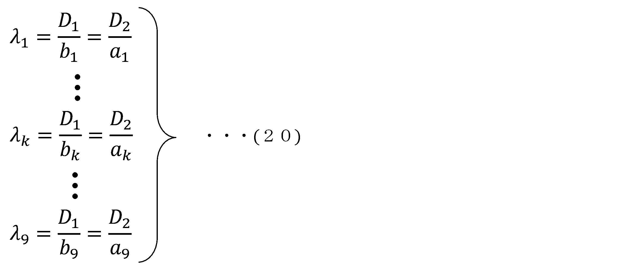
式(20)において、D1とD2は、第2の実施形態と同様に、それぞれ行方向に並ぶ光電変換部17-1-1~17-3-3の経路差D1であり、列方向に並ぶ光電変換部17-1-1~17-3-3の経路差D2である。kは、1~9の間の任意の自然数である。a1,…,ak,…,a9、及びb1,…,bk,…,b9は、任意の自然数である。
上記したように、波長λ1~λ9は、異なる波長であるため、a1~a9の各々は、異なる値になり、b1~b9の各々は、異なる値になる。ただし、ak=bkであってもよいし、ak≠bkであってもよい。したがって、波長λ1~λ9を選択する際の波長選択条件は、波長λ1~λ9の各々が異なる波長であるという条件と、式(20)を満足するという条件とを含む条件になる。この場合において、異なる波長λ1~λ9を定めてから、式(20)を満足するように、経路差D1と、経路差D2とを定めるようにしてもよいし、経路差D1と、経路差D2とを定めてから、波長選択条件を満たすように、波長λ1~λ9を定めるようにしてもよい。
上記の波長選択条件を満たすように選択された波長λ1~λ9を、例えば、図5に示すアレーアンテナ19aにおいて、符号90で示す送信指向性制御装置1aの本体が存在する方向からみて、図9(a)に示すように、波長λ1を「左上方向」、波長λ2を「左中方向」、波長λ3を「左下方向」、波長λ4を「中上方向」、波長λ5を「正面方向」、波長λ6を「中下方向」、波長λ7を「右上方向」、波長λ8を「右中方向」、波長λ9を「右下方向」に割り当てる。
さらに、第2の実施形態の送信指向性制御装置1aにおいて、第1走査用切替回路14Aと、第2走査用切替回路14Bとを光スイッチに替えて分波器とする。なお、この場合、操作部16aから、第1走査用切替回路14Aと、第2走査用切替回路14Bとに切替指示信号を出力する必要がなくなるため、第4の実施形態では、操作部16aを備える必要がなくなる。
第1走査用切替回路14A、及び第2走査用切替回路14Bの分波器が、以下のような分波を行うように設定する。第1走査用切替回路14Aの分波器が、入力端子14A-Sから供給される光信号を、波長λ1,λ4,λ7の光信号と、波長λ2,λ5,λ8の光信号と、波長λ3,λ6,λ9の光信号との3つのグループに分波するようにする。さらに、第1走査用切替回路14Aが備える分波器が、図9(b)に示すように、波長λ1,λ4,λ7の光信号を出力端子14A-E-3から出力し、波長λ2,λ5,λ8の光信号を出力端子14A-E-2から出力し、波長λ3,λ6,λ9の光信号を出力端子14A-E-1から出力するようにする。
第2走査用切替回路14Bの分波器が、入力端子14B-Sから供給される光信号を、波長λ1,λ2,λ3の光信号と、波長λ4,λ5,λ6の光信号と、波長λ7,λ8,λ9の光信号との3つのグループに分波するようにする。さらに、第2走査用切替回路14Bが備える分波器が、図9(c)に示すように、波長λ1,λ2,λ3の光信号を出力端子14B-E-1から出力し、波長λ4,λ5,λ6の光信号を出力端子14B-E-2から出力し、波長λ7,λ8,λ9の光信号を出力端子14B-E-3から出力するようにする。
第1走査用行列回路15Aが付与する位相傾斜は、入力端子15A-S-3から光信号が供給された場合に、送信ビームが上方向を向くような位相傾斜とし、入力端子15A-S-2から光信号が供給された場合に、送信ビームが正面方向を向くような位相傾斜とし、入力端子15A-S-1から光信号が供給された場合に、送信ビームが下方向を向くような位相傾斜とする。
第2走査用行列回路15Bが付与する位相傾斜は、入力端子15B-S-1から光信号が供給された場合に、送信ビームが左方向を向くような位相傾斜とし、入力端子15B-S-2から光信号が供給された場合に、送信ビームが正面方向を向くような位相傾斜とし、入力端子15B-S-3から光信号が供給された場合に、送信ビームが右方向を向くような位相傾斜とする。
第2の実施形態の送信指向性制御装置1aを、上記のような構成とした上で、図6に示す処理が、波長λ1~λ9ごとに行われる。これにより、異なる9つの波長λ1~λ9を用いて、9つの異なる送信信号1~送信信号9が重畳された9つの送信ビームを、並列に、図9(a)に示す9つの方向に送信することができる。
(第4の実施形態の効果)
上記した第4の実施形態のように構成した送信指向性制御装置1aは、9個の波長指定部10-1~10-9と、9個の光源11-1~11-9と、送信光信号生成部12aと、分波器に置き換えられた第1走査用切替回路14A及び第2走査用切替回路14Bとを備えることにより、波長多重を行うことが可能になる。この場合において、波長λ1~λ9は、上記した波長選択条件を満たす波長であるため、波長λ1~λ9の各々において、行方向において隣接する光電変換部17-i-jと、光電変換部17-(i+1)-jとに供給される上側帯波の光信号の位相差が2πの自然数倍になり、列方向において隣接する光電変換部17-i-jと、光電変換部17-i-(j+1)とに供給される搬送波の光信号の位相差が2πの自然数倍になる。その結果、波長λ1~λ9の各々において、行方向において隣接する光電変換部17-(i+1)-jと、光電変換部17-i-jとが出力するRF信号の位相差、及び、列方向において隣接する光電変換部17-i-(j+1)と、光電変換部17-i-jとが出力するRF信号の位相差は、第2の実施形態の場合と同一になる。そのため、第4の実施形態においても、第2の実施形態の送信指向性制御装置1aが有する効果を同一の効果を奏し、さらに、9つの送信ビームを並列に送信することができるマルチビームによる送信ができるという効果を有する。
上記した第4の実施形態のように構成した送信指向性制御装置1aは、9個の波長指定部10-1~10-9と、9個の光源11-1~11-9と、送信光信号生成部12aと、分波器に置き換えられた第1走査用切替回路14A及び第2走査用切替回路14Bとを備えることにより、波長多重を行うことが可能になる。この場合において、波長λ1~λ9は、上記した波長選択条件を満たす波長であるため、波長λ1~λ9の各々において、行方向において隣接する光電変換部17-i-jと、光電変換部17-(i+1)-jとに供給される上側帯波の光信号の位相差が2πの自然数倍になり、列方向において隣接する光電変換部17-i-jと、光電変換部17-i-(j+1)とに供給される搬送波の光信号の位相差が2πの自然数倍になる。その結果、波長λ1~λ9の各々において、行方向において隣接する光電変換部17-(i+1)-jと、光電変換部17-i-jとが出力するRF信号の位相差、及び、列方向において隣接する光電変換部17-i-(j+1)と、光電変換部17-i-jとが出力するRF信号の位相差は、第2の実施形態の場合と同一になる。そのため、第4の実施形態においても、第2の実施形態の送信指向性制御装置1aが有する効果を同一の効果を奏し、さらに、9つの送信ビームを並列に送信することができるマルチビームによる送信ができるという効果を有する。
上記した第2の実施形態の送信指向性制御装置1aを、第4の実施形態のように構成する手法は、第1の実施形態の送信指向性制御装置1、及び第3の実施形態の送信指向性制御装置1bに適用することが可能である。当該手法を、第1の実施形態の送信指向性制御装置1の構成に適用した場合、M個の送信ビームを並列に送信することが可能になる。さらに、アレーアンテナ19aの構成を3×3以外の構成とした第2の実施形態の送信指向性制御装置1a、及び第3の実施形態の送信指向性制御装置1bにも、当該手法を適用することができる。
(第5の実施形態)
図10は、第5の実施形態の送信指向性制御装置1cの構成例を示すブロック図である。第5の実施形態において、第1の実施形態と同一の構成については、同一の符号を付して説明する。送信指向性制御装置1cは、波長指定部10、光源11、送信光信号生成部12、重み付け部13、光電変換部17-1~17-M、及びアンテナ素子18-1~18-Mを備える。
図10は、第5の実施形態の送信指向性制御装置1cの構成例を示すブロック図である。第5の実施形態において、第1の実施形態と同一の構成については、同一の符号を付して説明する。送信指向性制御装置1cは、波長指定部10、光源11、送信光信号生成部12、重み付け部13、光電変換部17-1~17-M、及びアンテナ素子18-1~18-Mを備える。
第5の実施形態の送信指向性制御装置1cと、第1の実施形態の送信指向性制御装置1との構成上の違いは、以下の点である。第1の実施形態では、分波器22の光経路100が接続する出力端子を起点とし、光電変換部17-1~17-Mが並ぶ一列において隣接する2つの光電変換部17-1~17-Mの各々に到達するまでの光経路100の経路差が、一定の経路差Dになっていた。これに対して、第5の実施形態では、この経路差が、一定になっていない点である。
図10には、第5の実施形態の構成の一例を示している。図10において、2番目からM番目までの光電変換部17-2~17-Mについては、第1の実施形態と同様に、分波器22から隣接する光電変換部17-2~17-Mの各々に到達するまでの光経路100の経路差を、経路差Dとしている。これに対して、光電変換部17-1と、光電変換部17-2とについては、光経路100の経路を、経路差Dとしていない。
このような場合であっても、光電変換部17-1と、光電変換部17-2との光経路100の経路差を、図10に示す例のように、波長λの任意の自然数倍とすれば、第1の実施形態と同様に、光電変換部17-1~17-Mの各々に供給される搬送波の光信号において経路差のために生じる位相差を吸収することができる。
第5の実施形態の送信指向性制御装置1cの構成を、更に一般化して示すために、「j」を1~Mの間の任意の自然数とし、mjを任意の自然数とする。光電変換部17-1~17-Mにおいて、隣接する光電変換部17-(j-1)と、光電変換部17-jの間の光経路100の経路差を、波長λ×mjとする。ただし、j=1の場合、光電変換部17-0が存在しないため、m1=0とする。この場合、光電変換部17-jが出力するRF信号は、次式(21)で示され、光電変換部17-(j+1)が出力するRF信号は、次式(22)で示される。


式(22)の右辺の式と、式(21)の右辺の式との位相差は、「-φj+1+φj+2mj+1π」になる。図10では、一例として、光電変換部17-1と、光電変換部17-2との光経路100の経路差を、経路差Dの2倍とした例を示している。この場合、光電変換部17-1と、光電変換部17-2との間の光経路100の経路差は、「2aλ」であるため、m2は、「2a」になる。したがって、位相差は、「-φ2+φ1+4aπ」になる。光電変換部17-2以降については、光経路100の経路差が、「aλ」になるため、mj+1は、「a」になる。したがって、位相差は、「-φj+1+φj+2aπ」になる。
すなわち、いずれの場合においても、mj+1が自然数であるため、「2mj+1π」は、2πの自然数倍になる。そのため、「-φj+1+φj+2mj+1π」が示す位相は、「-φj+1+φj」に一致し、搬送波の光信号が光電変換部17-1~17-Mの各々に到達するまでの光経路100の経路差によって、光電変換部17-1~17-Mの各々に供給される搬送波の光信号に生じる位相差が吸収されることになる。そのため、第1の実施形態と同様に、隣接する光電変換部17-(j+1)と、光電変換部17-jとが出力するRF信号の位相差を、走査用行列回路15によって付与される位相傾斜「-φj+1+φj」にすることができる。
(第5の実施形態の効果)
第5の実施形態では、分波器22の光経路100が接続する出力端子を起点とし、隣接する2つの光電変換部17-1~17-Mの各々に到達するまでの光経路100の経路差が、一定になっていない場合であっても、経路差の各々を、波長λの任意の自然数倍にするようにしている。これにより、隣接する光電変換部17-(j+1)と、光電変換部17-jとが出力するRF信号の位相差を、走査用行列回路15によって付与される位相傾斜「-φj+1+φj」にすることができる。そのため、これらのRF信号を用いることにより、アンテナ素子18-1~18-Mから放射されるRF信号の電波を、ユーザが所望する送信方向に伝搬させることが可能になる。
第5の実施形態では、分波器22の光経路100が接続する出力端子を起点とし、隣接する2つの光電変換部17-1~17-Mの各々に到達するまでの光経路100の経路差が、一定になっていない場合であっても、経路差の各々を、波長λの任意の自然数倍にするようにしている。これにより、隣接する光電変換部17-(j+1)と、光電変換部17-jとが出力するRF信号の位相差を、走査用行列回路15によって付与される位相傾斜「-φj+1+φj」にすることができる。そのため、これらのRF信号を用いることにより、アンテナ素子18-1~18-Mから放射されるRF信号の電波を、ユーザが所望する送信方向に伝搬させることが可能になる。
したがって、第5の実施形態の送信指向性制御装置1cは、第1の実施形態の送信指向性制御装置1と同様の効果を奏するので、アレーアンテナ19の規模が大きくなっても、配線構造を複雑にすることなく、適切な重み付けを可能とし、小型化及び量産化に適した簡易な構造の回路による送信指向性の制御ができる。
第5の実施形態の送信指向性制御装置1cの隣接する2つの光電変換部17-1~17-Mの各々に到達するまでの光経路100の経路差を、一定にせず、経路差の各々を、波長λの任意の自然数倍にする手法は、アレーアンテナ19が、2次元に配置されたアレーアンテナ19aを備える第2から第4の実施形態にも適用が可能であり、さらに、第2から第4の実施形態において、アンテナ素子18-1-1~18-3-3の数を増加させた構成に対しても適用が可能である。
(各実施形態に共通する効果)
第1から第5の実施形態では、光信号のアナログ処理で移相を実現していることから、電波を放射する際のビーム走査だけでなく、空間光無線通信(いわゆるFSO(Free Space Optics)通信)等において、光を放射する際のビーム走査を、機械駆動ではなく電子的に行う回路に、第1から第5の実施形態の送信指向性制御装置1~1cの仕組みを応用することができる。現状のFSO通信では、放射方向を機械駆動装置により調整しているため、装置の重量や量産性の課題が想定され、また、動作速度や耐久性の観点において、運用や保守の課題が想定される。このような課題を有するFSO通信に対して、第1から第5の実施形態の送信指向性制御装置1~1cの仕組みを応用することによって、光ビームの電子的な走査が可能になれば、これらの課題を解決することが可能になる。
第1から第5の実施形態では、光信号のアナログ処理で移相を実現していることから、電波を放射する際のビーム走査だけでなく、空間光無線通信(いわゆるFSO(Free Space Optics)通信)等において、光を放射する際のビーム走査を、機械駆動ではなく電子的に行う回路に、第1から第5の実施形態の送信指向性制御装置1~1cの仕組みを応用することができる。現状のFSO通信では、放射方向を機械駆動装置により調整しているため、装置の重量や量産性の課題が想定され、また、動作速度や耐久性の観点において、運用や保守の課題が想定される。このような課題を有するFSO通信に対して、第1から第5の実施形態の送信指向性制御装置1~1cの仕組みを応用することによって、光ビームの電子的な走査が可能になれば、これらの課題を解決することが可能になる。
(各実施形態における他の構成例)
第1の実施形態において、アンテナ素子18-1~18-Mに給電するRF信号の位相傾斜誤差(以下、給電位相傾斜誤差という)に許容範囲があり、例えば、分波器22の光経路100が接続する出力端子から最も光経路100の経路長が最も近いアンテナ素子18-1の給電位相傾斜誤差をθ°とする。この場合、経路差Dを、次式(23)によって定める。
第1の実施形態において、アンテナ素子18-1~18-Mに給電するRF信号の位相傾斜誤差(以下、給電位相傾斜誤差という)に許容範囲があり、例えば、分波器22の光経路100が接続する出力端子から最も光経路100の経路長が最も近いアンテナ素子18-1の給電位相傾斜誤差をθ°とする。この場合、経路差Dを、次式(23)によって定める。

経路差Dが、式(23)によって定められる場合、光電変換部17-jが出力するRF信号は、式(8)に替えて、次式(24)で示される。

式(24)は、式(25)に変形することができる。

光電変換部17-jに隣接する光電変換部17-(j+1)が出力するRF信号は、式(25)の「j」に「j+1」を代入して得られるため、次式(26)として示される。

式(26)の右辺と、式(25)の右辺との位相差は、「-φj+1+φj+2aπ±θ°π/180」になる。「θ°π/180」は、「θ°」をラジアンで表した場合の値になる。「2aπ」は、2πの「a」倍であり、「a」は自然数である。したがって、当該位相差が示す位相は、「-φj+1+φj±θ°π/180」に一致する。そのため、搬送波の光信号が光電変換部17-1~17-Mの各々に到達するまでの光経路100の経路差「aλ」によって、光電変換部17-1~17-Mの各々に供給される搬送波の光信号に生じる位相差「2aπ」を吸収しつつ、アンテナ素子18-1~18-Mに対して、給電位相傾斜誤差θ°の範囲内でRF信号を供給することが可能になる。
給電位相傾斜誤差θ°を考慮して、経路差を定める手法は、第5の実施形態に対しても同様に適用することが可能である。また、当該手法は、アレーアンテナ19が、2次元に配置されたアレーアンテナ19aを備える第2から第4の実施形態にも適用が可能であり、さらに、第2から第4の実施形態において、アンテナ素子18-1-1~18-3-3の数を増加させた構成に対しても適用が可能である。
第1、第2、第3、及び第5の実施形態に示す送信光信号生成部12を、図11に示す送信光信号生成部12bに置き換えてもよい。送信光信号生成部12bは、SSB(Single Side Band)光変調器26と、分波器22とを備える。SSB光変調器26は、光源11が生成する波長λの光を、送信信号でSSB変調する。ここで、SSB光変調器26が行うSSB変調は、強度変調する際に、下側波帯を抑制して、強度変調を行う変調である。したがって、SSB光変調器26は、搬送波の光信号と、上側帯波の光信号とを含む被変調光信号を生成する。分波器22は、SSB光変調器26が生成して出力する被変調光信号を、搬送波の光信号と、上側帯波の光信号とに分波し、分波した搬送波の光信号を光経路100に出力し、分波した上側帯波の光信号を光経路200に出力する。
第1、第2、第3、及び第5の実施形態に示す送信光信号生成部12を、図12に示す送信光信号生成部12cに置き換えてもよい。送信光信号生成部12cは、分配器27と、SSB光変調器26aとを備える。分配器27は、光源11が生成して出力する波長λの光を2つの光に分配し、分配した一方を、光経路100に出力し、他方をSSB光変調器26aに出力する。すなわち、光源11が生成した波長λの光が、そのまま搬送波の光信号として、光経路100に出力される。SSB光変調器26aは、分配器27が出力する光を、送信信号でSSB変調する。ここで、SSB光変調器26aが行うSSB変調とは、例えば、強度変調する際に、搬送波の周波数帯と、下側波帯とを抑制して、強度変調を行う変調である。したがって、SSB光変調器26aは、上側帯波の光信号を、被変調光信号として生成し、生成した上側帯波の光信号を光経路200に出力する。
なお、図8に示す第4の実施形態の送信光信号生成部12aの光変調器21-1~21-9に替えて、図11に示すSSB光変調器26を適用してもよい。また、図8に示す第4の実施形態の送信光信号生成部12aから光コムフィルタ24を取り除き、光変調器21-1~21-9に替えて、図12に示す分配器27と、SSB光変調器26aとを、それぞれ9個、備えるようにして、9個の分配器27が出力する搬送波の光信号となる光を合波する合波器と、9個のSSB光変調器26aが出力する上側帯波の光信号を合波する合波器とを備えるようにしてもよい。また、図8に示す送信光信号生成部12aとして、合波器23の出力に2分配する分配器を備えて、分配器の2つの出力に1入力1出力の光コムフィルタをそれぞれ接続して、一方の光コムフィルタから搬送波の合波光信号を出力し、他方の光コムフィルタから上側帯波の合波光信号を出力するようにしてもよい。
上記した各実施形態において、送信光信号生成部12,12a,12b,12cは、強度変調して、周波数帯域の異なる搬送波の光信号と、上側帯波の光信号とを生成している。これに対して、送信光信号生成部12,12a,12b,12cは、搬送波の光信号と、上側帯波の光信号とを生成することに限られず、以下に示す例のような、異なる周波数帯域の2つの光信号である第1光信号と、第2光信号とを生成するようにしてもよい。例えば、送信光信号生成部12,12a,12b,12cは、搬送波の光信号と、上側帯波の光信号とを生成することに替えて、搬送波の光信号と、下側帯波の光信号とを生成するようにしてもよい。また、送信光信号生成部12,12a,12b,12cは、搬送波の光信号と、上側帯波の光信号とを生成することに替えて、上側帯波の光信号と、下側帯波の光信号とを生成するようにしてもよい。
上記の各実施形態では、光経路100によって、搬送波の光信号が伝送され、光経路200によって、上側帯波の光信号が伝送されるようにしている。ここで、光経路100によって伝送される光信号を第1光信号、光経路200によって伝送される光信号を第2光信号とする。この場合、第1光信号と、第2光信号との組み合わせは、上記した搬送波の光信号と、上側帯波の光信号との組み合わせに限られず、逆の上側帯波の光信号と、搬送波の光信号との組み合わせであってもよく、また、上記した搬送波の光信号と、下側帯波の光信号の組み合わせ、及び、当該組み合わせの逆の組み合わせであってもよく、上記した上側帯波の光信号と、下側帯波の光信号との組み合わせ、及び、当該組み合わせの逆の組み合わせであってもよい。
第1、及び第5の実施形態に示す光電変換部17-1~17-Mにおいて、合波器32-1~32-Mを、いわゆるハーフミラーに置き換えるようにしてもよい。具体的には、光電変換部17-jを、図13に示す光電変換部17a-jに置き換える。光電変換部17a-jは、合波器32-jに替えて、いわゆるハーフミラーであるミラー33-jを備える。ミラー33-jは、分岐光経路102-jを介して供給される搬送波の光信号を反射して、PD31-jの方向に進行させ、光経路200-jを介してから供給される上側帯波の光信号を透過させて、PD31-jの方向に進行させることにより、搬送波の光信号と、上側帯波の光信号とを合波する。逆に、上側帯波の光信号を反射し、搬送波の光信号を透過させる形態であってもよい。同様に、第2から第4の実施形態に示す光電変換部17-1-1~17-3-3が備える合波器32-1-1~32-3-3を、ハーフミラーに置き換えるようにしてもよい。
第1の実施形態において示した第1接続条件を満たす光電変換部17-1~17-Mを等間隔に配置する構成や、第2の実施形態において示した第2接続条件を満たす光電変換部17-1-1~17-3-3において行方向の隣接間隔を同一とし、列方向の隣接間隔を同一とする構成は、上記したように一例である。第1接続条件を満たす限りにおいて、第1の実施形態において、光電変換部17-1~17-Mが等間隔で配置されていない構成であってもよい。第2接続条件を満たす限りにおいて、第2の実施形態において、光電変換部17-1-1~17-3-3において行方向の隣接間隔が同一になっていなくてもよく、列方向の隣接間隔が同一になっていなくてもよい。これは、第3及び第4の実施形態においても同様である。また、第5の実施形態では、分波器22の光経路100が接続する出力端子を起点とし、光電変換部17-1~17-Mにおいて隣接する2つの光電変換部17-1~17-Mの各々に到達するまでの光経路の経路差の各々が、一定にならないように、光電変換部17-1~17-Mが配置されていれば、どのように配置されていてもよく、光電変換部17-1~17-Mが等間隔に配置されていてもよい。これは、第5の実施形態の手法が適用される第2から第4の実施形態においても同様である。
上記の各実施形態において、光電変換部17-1~17-M,17-1-1~17-3-3の各々と、各々に接続するアンテナ素子18-1~18-M,18-1-1~18-3-3との間の電気配線の配線長は、同一長であることが望ましいが、一般的な回路構成において割り当てられる程度の長さであればよく、厳密に同一の長さになっていなくてもよい。
上記した第1の実施形態において、アンテナ素子18-1~18-Mの配置の指標となる配置線に沿って光電変換部17-1~17-Mを一列に並べるという一例を示している。これに対して、第1、及び第5の実施形態において、光電変換部17-1~17-Mが並ぶ一列は、配置線に沿っていなくてもよい。上記した第2の実施形態において、光電変換部17-1-1~17-3-3における行方向が、第1配置線の方向に一致し、列方向が、第2配置線の方向に一致するという一例を示している。これに対して、第2から第4の実施形態において、行方向が、第1配置線に対応し、列方向が、第2配置線に対応するという対応関係になっていれば、現実の行方向に並べられる光電変換部17-1-1~17-3-3の向きが、第1配置線の方向に一致していなくてもよいし、現実の列方向に並べられる光電変換部17-1-1~17-3-3の向きが、第2配置線の方向に一致していなくてもよい。
上記の各実施形態において、光源11,11-1~11-9は、波長可変光源であり、波長指定部10,10-1~10-9から受ける波長指定信号に含まれている波長の光を生成するとしている。これに対して、光源11,11-1~11-9を、波長可変光源ではなく、単一の波長を生成して出力する光源とし、波長指定部10,10-1~10-9を備えない構成としてもよい。この場合、光源11として、ユーザが定める波長λを生成する光源を選択して用いることになり、光源11-1~11-9の各々として、各ユーザが定める波長λ1~λ9の各々を生成する光源を選択して用いることになる。
上記の各実施形態において図面に示す分波器22,42-1~42-3、及び合波器23,32-j,41-1~41-3、並びに、本文において言及した分波器、及び合波器は、例えば、AWG(Arrayed Waveguide Grating)であってもよいし、AWG以外の光学素子によって構成されるものであってもよい。
上記の各実施形態において示す光電変換部17-1~17-M,17-1-1~17-3-3,17a-jは、RF信号を生成するとしているが、RF信号を含むより広い周波数帯域の電磁波の電気信号を生成し、アンテナ素子18-1~18-M,18-1-1~18-3-3から電波を含むより広い周 波数帯域の電磁波を放射するようにしてもよい。
上記の各実施形態において、走査用行列回路15,15A,15B,15Cは、傾斜位相量を付与しない光信号を出力しないようにしてもよい。
以上、この発明の実施形態について図面を参照して詳述してきたが、具体的な構成はこの実施形態に限られるものではなく、この発明の要旨を逸脱しない範囲の設計等も含まれる。
ミリ波帯やテラヘルツ帯の高周波帯の電波を用いた無線伝送、イメージング、レーダ等において形成される高い指向性を有する電磁波の送信に適用することができる。
1…送信指向性制御装置、10…波長指定部、11…光源、12…送信光信号生成部、13…重み付け部、14…走査用切替回路、14-S…入力端子、14-E-1~14-E-M…出力端子、15…走査用行列回路、15-S-1~15-S-M…入力端子、15-E-1~15-E-M…出力端子、16…操作部、17-1~17-M…光電変換部、18-1~18-M…アンテナ素子、80,81,82…方向、100,200…光経路、101-1~101-M…分岐点、102-1~102-M…分岐光経路
Claims (8)
- 3次元空間において任意に定められる配置線に沿って配置される複数のアンテナ素子と、
光を送信信号で変調して、異なる周波数帯域の第1光信号と、第2光信号とを生成する送信光信号生成部と、
前記第2光信号に対して、前記配置線の方向と、所望する送信方向とに応じて予め定められる位相傾斜を付与して、前記配置線に沿って配置される前記アンテナ素子の各々に対応する位相傾斜付きの第2光信号を生成する重み付け部と、
前記アンテナ素子の各々に対応して備えられ、一列に並べられる光電変換部の各々であって、各々に対応する前記位相傾斜付きの第2光信号と、前記第1光信号とを合成して電気信号に変換し、変換した前記電気信号を、各々に対応する前記アンテナ素子に出力する光電変換部と、を備え、
前記光電変換部の各々が合成する2つの光信号の何れか一方の光信号に生じる位相差であって、当該一方の光信号が前記光電変換部の各々に到達するまでの光経路の経路差によって生じる位相差が吸収されるように、前記一列において隣接する前記光電変換部の間の光経路の経路差の各々と、前記光の波長とを選択する、
送信指向性制御装置。 - 前記配置線を第2配置線とし、前記第2配置線に交差する第1配置線に沿って、更に、複数の前記アンテナ素子が配置されてアレーアンテナが形成されており、
前記重み付け部は、
前記第1光信号に対して、前記第1配置線の方向と、前記所望する送信方向とに応じて予め定められる位相傾斜を付与して、前記第1配置線に沿って配置される前記アンテナ素子の各々に対応する位相傾斜付きの第1光信号を生成し、
前記光電変換部は、
前記第1配置線の方向に対応する行方向と、前記第2配置線の方向に対応する列方向とに沿って、行列形状に配置されており、
前記光電変換部の各々は、
各々に対応する前記位相傾斜付きの第2光信号と、前記第1光信号とを合成して電気信号に変換することに替えて、各々に対応する前記位相傾斜付きの第1光信号と、各々に対応する前記位相傾斜付きの第2光信号とを合成して電気信号に変換し、変換した前記電気信号を、各々に対応する前記アンテナ素子に出力し、
前記位相傾斜付きの第1光信号が列方向の前記光電変換部の各々に到達するまでの光経路の経路差によって前記位相傾斜付きの第1光信号に生じる位相差が吸収されるように、かつ、前記位相傾斜付きの第2光信号が行方向の前記光電変換部の各々に到達するまでの光経路の経路差によって前記位相傾斜付きの第2光信号に生じる位相差が吸収されるように、列方向において隣接する前記光電変換部の間の光経路の経路差の各々と、行方向において隣接する前記光電変換部の間の光経路の経路差の各々と、前記光の波長とを選択する、
請求項1に記載の送信指向性制御装置。 - 隣接する前記光電変換部の間の光経路の経路差の各々が、前記光の波長に、所定値を乗算した乗算値の何れかの乗算値に一致するように、隣接する前記光電変換部の間の光経路の経路差の各々を予め定めて前記光の波長を選択するか、または、前記光の波長を予め定めて隣接する前記光電変換部の間の光経路の経路差の各々を定める、
請求項1または請求項2に記載の送信指向性制御装置。 - 前記所定値は、任意の自然数である、
請求項3に記載の送信指向性制御装置。 - 前記所定値は、前記到達するまでの光経路の経路長が最も短い前記光電変換部が出力する前記電気信号において許容される誤差をθ°とした場合、任意の自然数に対してθ°/360を加算、または、減算して得られる値である、
請求項3に記載の送信指向性制御装置。 - 隣接する前記光電変換部の間の光経路の経路差の全てが同一であるか、または、隣接する前記光電変換部の間の光経路の経路差の全部、もしくは、一部が異なる、
請求項4に記載の送信指向性制御装置。 - 隣接する前記光電変換部の間の光経路の経路差の全てが同一であるか、または、隣接する前記光電変換部の間の光経路の経路差の全部、もしくは、一部が異なる、
請求項5に記載の送信指向性制御装置。 - 3次元空間において任意に定められる配置線に沿って配置される複数のアンテナ素子に対する送信指向性制御方法であって、
送信光信号生成部が、光を送信信号で変調して、異なる周波数帯域の第1光信号と、第2光信号とを生成するステップと、
重み付け部が、前記第2光信号に対して、前記配置線の方向と、所望する送信方向とに応じて予め定められる位相傾斜を付与して、前記配置線に沿って配置される前記アンテナ素子の各々に対応する位相傾斜付きの第2光信号を生成するステップと、
前記アンテナ素子の各々に対応して備えられ、一列に並べられる光電変換部の各々が、各々に対応する前記位相傾斜付きの第2光信号と、前記第1光信号とを合成して電気信号に変換し、変換した前記電気信号を、各々に対応する前記アンテナ素子に出力するステップと、を含み、
前記光電変換部の各々が合成する2つの光信号の何れか一方の光信号に生じる位相差であって、当該一方の光信号が前記光電変換部の各々に到達するまでの光経路の経路差によって生じる位相差が吸収されるように、前記一列において隣接する前記光電変換部の間の光経路の経路差の各々と、前記光の波長とを選択する、
送信指向性制御方法。
Priority Applications (2)
| Application Number | Priority Date | Filing Date | Title |
|---|---|---|---|
| JP2025533748A JPWO2025017809A1 (ja) | 2023-07-14 | 2023-07-14 | |
| PCT/JP2023/026143 WO2025017809A1 (ja) | 2023-07-14 | 2023-07-14 | 送信指向性制御装置、及び送信指向性制御方法 |
Applications Claiming Priority (1)
| Application Number | Priority Date | Filing Date | Title |
|---|---|---|---|
| PCT/JP2023/026143 WO2025017809A1 (ja) | 2023-07-14 | 2023-07-14 | 送信指向性制御装置、及び送信指向性制御方法 |
Publications (1)
| Publication Number | Publication Date |
|---|---|
| WO2025017809A1 true WO2025017809A1 (ja) | 2025-01-23 |
Family
ID=94281833
Family Applications (1)
| Application Number | Title | Priority Date | Filing Date |
|---|---|---|---|
| PCT/JP2023/026143 Pending WO2025017809A1 (ja) | 2023-07-14 | 2023-07-14 | 送信指向性制御装置、及び送信指向性制御方法 |
Country Status (2)
| Country | Link |
|---|---|
| JP (1) | JPWO2025017809A1 (ja) |
| WO (1) | WO2025017809A1 (ja) |
Cited By (1)
| Publication number | Priority date | Publication date | Assignee | Title |
|---|---|---|---|---|
| CN121396342A (zh) * | 2025-12-24 | 2026-01-23 | 苏州爱雄斯通信技术有限公司 | 射频光网络前回传信号的波分隔离抗干扰方法及系统 |
Citations (3)
| Publication number | Priority date | Publication date | Assignee | Title |
|---|---|---|---|---|
| WO2003079101A1 (es) * | 2002-03-15 | 2003-09-25 | Universidad Politecnica De Valencia | Red conformadora de haces para agrupaciones de antenas basada en matrices ópticas de elementos desfasadores/retardadores fijos |
| JP2010028236A (ja) * | 2008-07-15 | 2010-02-04 | Mitsubishi Electric Corp | 光制御型マルチビームアンテナ装置 |
| US20230093054A1 (en) * | 2021-09-22 | 2023-03-23 | Apple Inc. | Electronic Devices with Shared Phase Shifting for High Frequency Communication |
-
2023
- 2023-07-14 WO PCT/JP2023/026143 patent/WO2025017809A1/ja active Pending
- 2023-07-14 JP JP2025533748A patent/JPWO2025017809A1/ja active Pending
Patent Citations (3)
| Publication number | Priority date | Publication date | Assignee | Title |
|---|---|---|---|---|
| WO2003079101A1 (es) * | 2002-03-15 | 2003-09-25 | Universidad Politecnica De Valencia | Red conformadora de haces para agrupaciones de antenas basada en matrices ópticas de elementos desfasadores/retardadores fijos |
| JP2010028236A (ja) * | 2008-07-15 | 2010-02-04 | Mitsubishi Electric Corp | 光制御型マルチビームアンテナ装置 |
| US20230093054A1 (en) * | 2021-09-22 | 2023-03-23 | Apple Inc. | Electronic Devices with Shared Phase Shifting for High Frequency Communication |
Cited By (1)
| Publication number | Priority date | Publication date | Assignee | Title |
|---|---|---|---|---|
| CN121396342A (zh) * | 2025-12-24 | 2026-01-23 | 苏州爱雄斯通信技术有限公司 | 射频光网络前回传信号的波分隔离抗干扰方法及系统 |
Also Published As
| Publication number | Publication date |
|---|---|
| JPWO2025017809A1 (ja) | 2025-01-23 |
Similar Documents
| Publication | Publication Date | Title |
|---|---|---|
| US6535165B2 (en) | Phased array antenna beamformer | |
| JP7328578B2 (ja) | 無線送信システム、無線受信システム、基地局装置、及び無線通信システム、並びに無線送信方法、及び無線受信方法 | |
| US9748648B2 (en) | Distributed feeding device for antenna beamforming | |
| JP7701670B2 (ja) | 送信指向性制御装置及び送信指向性制御方法 | |
| US8400355B1 (en) | Passive photonic dense wavelength-division multiplexing true-time-delay system | |
| JP7701669B2 (ja) | 送信指向性制御装置及び送信指向性制御方法 | |
| Ortega et al. | Optical beamformer for 2-D phased array antenna with subarray partitioning capability | |
| JP7744611B2 (ja) | 送信指向性制御装置及び送信指向性制御方法 | |
| JP4632444B2 (ja) | 光制御アレイアンテナ装置 | |
| US9397397B2 (en) | Electronically-steered Ku-band phased array antenna comprising an integrated photonic beamformer | |
| JP7323826B2 (ja) | 無線送信システム、無線受信システム、基地局装置、及び無線通信システム、並びに無線送信方法、及び無線受信方法 | |
| Belkin et al. | Design and Optimization of Photonics-Based Beamforming | |
| WO2025017809A1 (ja) | 送信指向性制御装置、及び送信指向性制御方法 | |
| JP7817629B2 (ja) | 送信指向性制御装置、送信システム及び送信指向性制御方法 | |
| JP4475592B2 (ja) | 光制御型アレーアンテナ装置 | |
| CN117938271A (zh) | 微波光子一体化接收处理装置 | |
| WO2025017811A1 (ja) | 送信指向性制御装置、及び送信指向性制御方法 | |
| JP7751241B2 (ja) | 送信指向性制御装置、および制御方法 | |
| Thai et al. | A novel simplified dual beam-former using multichannel chirped fiber grating and tunable optical delay lines | |
| JP4974871B2 (ja) | アンテナ装置 | |
| WO2026074701A1 (ja) | 送信指向性制御装置 | |
| EP4465080A2 (en) | Optical beam forming device with crossbar as beamformer and its method of use | |
| JP7755208B2 (ja) | 受信指向性制御装置及び受信指向性制御方法 | |
| Fito et al. | Design requirements for mm-wave integrated optical beamforming networks | |
| WO2024134762A1 (ja) | 受信指向性制御装置及び受信指向性制御方法 |
Legal Events
| Date | Code | Title | Description |
|---|---|---|---|
| 121 | Ep: the epo has been informed by wipo that ep was designated in this application |
Ref document number: 23945814 Country of ref document: EP Kind code of ref document: A1 |
|
| ENP | Entry into the national phase |
Ref document number: 2025533748 Country of ref document: JP Kind code of ref document: A |
|
| WWE | Wipo information: entry into national phase |
Ref document number: 2025533748 Country of ref document: JP |
|
| NENP | Non-entry into the national phase |
Ref country code: DE |