WO2025017415A1 - 製造装置、及び酸化物半導体層の作製方法 - Google Patents
製造装置、及び酸化物半導体層の作製方法 Download PDFInfo
- Publication number
- WO2025017415A1 WO2025017415A1 PCT/IB2024/056604 IB2024056604W WO2025017415A1 WO 2025017415 A1 WO2025017415 A1 WO 2025017415A1 IB 2024056604 W IB2024056604 W IB 2024056604W WO 2025017415 A1 WO2025017415 A1 WO 2025017415A1
- Authority
- WO
- WIPO (PCT)
- Prior art keywords
- layer
- oxide semiconductor
- semiconductor layer
- oxide
- chamber
- Prior art date
- Legal status (The legal status is an assumption and is not a legal conclusion. Google has not performed a legal analysis and makes no representation as to the accuracy of the status listed.)
- Pending
Links
Images


Classifications
-
- C—CHEMISTRY; METALLURGY
- C23—COATING METALLIC MATERIAL; COATING MATERIAL WITH METALLIC MATERIAL; CHEMICAL SURFACE TREATMENT; DIFFUSION TREATMENT OF METALLIC MATERIAL; COATING BY VACUUM EVAPORATION, BY SPUTTERING, BY ION IMPLANTATION OR BY CHEMICAL VAPOUR DEPOSITION, IN GENERAL; INHIBITING CORROSION OF METALLIC MATERIAL OR INCRUSTATION IN GENERAL
- C23C—COATING METALLIC MATERIAL; COATING MATERIAL WITH METALLIC MATERIAL; SURFACE TREATMENT OF METALLIC MATERIAL BY DIFFUSION INTO THE SURFACE, BY CHEMICAL CONVERSION OR SUBSTITUTION; COATING BY VACUUM EVAPORATION, BY SPUTTERING, BY ION IMPLANTATION OR BY CHEMICAL VAPOUR DEPOSITION, IN GENERAL
- C23C14/00—Coating by vacuum evaporation, by sputtering or by ion implantation of the coating forming material
- C23C14/06—Coating by vacuum evaporation, by sputtering or by ion implantation of the coating forming material characterised by the coating material
- C23C14/08—Oxides
-
- C—CHEMISTRY; METALLURGY
- C23—COATING METALLIC MATERIAL; COATING MATERIAL WITH METALLIC MATERIAL; CHEMICAL SURFACE TREATMENT; DIFFUSION TREATMENT OF METALLIC MATERIAL; COATING BY VACUUM EVAPORATION, BY SPUTTERING, BY ION IMPLANTATION OR BY CHEMICAL VAPOUR DEPOSITION, IN GENERAL; INHIBITING CORROSION OF METALLIC MATERIAL OR INCRUSTATION IN GENERAL
- C23C—COATING METALLIC MATERIAL; COATING MATERIAL WITH METALLIC MATERIAL; SURFACE TREATMENT OF METALLIC MATERIAL BY DIFFUSION INTO THE SURFACE, BY CHEMICAL CONVERSION OR SUBSTITUTION; COATING BY VACUUM EVAPORATION, BY SPUTTERING, BY ION IMPLANTATION OR BY CHEMICAL VAPOUR DEPOSITION, IN GENERAL
- C23C14/00—Coating by vacuum evaporation, by sputtering or by ion implantation of the coating forming material
- C23C14/22—Coating by vacuum evaporation, by sputtering or by ion implantation of the coating forming material characterised by the process of coating
- C23C14/34—Sputtering
-
- C—CHEMISTRY; METALLURGY
- C23—COATING METALLIC MATERIAL; COATING MATERIAL WITH METALLIC MATERIAL; CHEMICAL SURFACE TREATMENT; DIFFUSION TREATMENT OF METALLIC MATERIAL; COATING BY VACUUM EVAPORATION, BY SPUTTERING, BY ION IMPLANTATION OR BY CHEMICAL VAPOUR DEPOSITION, IN GENERAL; INHIBITING CORROSION OF METALLIC MATERIAL OR INCRUSTATION IN GENERAL
- C23C—COATING METALLIC MATERIAL; COATING MATERIAL WITH METALLIC MATERIAL; SURFACE TREATMENT OF METALLIC MATERIAL BY DIFFUSION INTO THE SURFACE, BY CHEMICAL CONVERSION OR SUBSTITUTION; COATING BY VACUUM EVAPORATION, BY SPUTTERING, BY ION IMPLANTATION OR BY CHEMICAL VAPOUR DEPOSITION, IN GENERAL
- C23C16/00—Chemical coating by decomposition of gaseous compounds, without leaving reaction products of surface material in the coating, i.e. chemical vapour deposition [CVD] processes
- C23C16/22—Chemical coating by decomposition of gaseous compounds, without leaving reaction products of surface material in the coating, i.e. chemical vapour deposition [CVD] processes characterised by the deposition of inorganic material, other than metallic material
- C23C16/30—Deposition of compounds, mixtures or solid solutions, e.g. borides, carbides, nitrides
- C23C16/40—Oxides
-
- C—CHEMISTRY; METALLURGY
- C23—COATING METALLIC MATERIAL; COATING MATERIAL WITH METALLIC MATERIAL; CHEMICAL SURFACE TREATMENT; DIFFUSION TREATMENT OF METALLIC MATERIAL; COATING BY VACUUM EVAPORATION, BY SPUTTERING, BY ION IMPLANTATION OR BY CHEMICAL VAPOUR DEPOSITION, IN GENERAL; INHIBITING CORROSION OF METALLIC MATERIAL OR INCRUSTATION IN GENERAL
- C23C—COATING METALLIC MATERIAL; COATING MATERIAL WITH METALLIC MATERIAL; SURFACE TREATMENT OF METALLIC MATERIAL BY DIFFUSION INTO THE SURFACE, BY CHEMICAL CONVERSION OR SUBSTITUTION; COATING BY VACUUM EVAPORATION, BY SPUTTERING, BY ION IMPLANTATION OR BY CHEMICAL VAPOUR DEPOSITION, IN GENERAL
- C23C16/00—Chemical coating by decomposition of gaseous compounds, without leaving reaction products of surface material in the coating, i.e. chemical vapour deposition [CVD] processes
- C23C16/44—Chemical coating by decomposition of gaseous compounds, without leaving reaction products of surface material in the coating, i.e. chemical vapour deposition [CVD] processes characterised by the method of coating
- C23C16/455—Chemical coating by decomposition of gaseous compounds, without leaving reaction products of surface material in the coating, i.e. chemical vapour deposition [CVD] processes characterised by the method of coating characterised by the method used for introducing gases into reaction chamber or for modifying gas flows in reaction chamber
-
- H—ELECTRICITY
- H10—SEMICONDUCTOR DEVICES; ELECTRIC SOLID-STATE DEVICES NOT OTHERWISE PROVIDED FOR
- H10P—GENERIC PROCESSES OR APPARATUS FOR THE MANUFACTURE OR TREATMENT OF DEVICES COVERED BY CLASS H10
- H10P14/00—Formation of materials, e.g. in the shape of layers or pillars
- H10P14/20—Formation of materials, e.g. in the shape of layers or pillars of semiconductor materials
- H10P14/29—Formation of materials, e.g. in the shape of layers or pillars of semiconductor materials characterised by the substrates
-
- H—ELECTRICITY
- H10—SEMICONDUCTOR DEVICES; ELECTRIC SOLID-STATE DEVICES NOT OTHERWISE PROVIDED FOR
- H10P—GENERIC PROCESSES OR APPARATUS FOR THE MANUFACTURE OR TREATMENT OF DEVICES COVERED BY CLASS H10
- H10P30/00—Ion implantation into wafers, substrates or parts of devices
- H10P30/20—Ion implantation into wafers, substrates or parts of devices into semiconductor materials, e.g. for doping
-
- H—ELECTRICITY
- H10—SEMICONDUCTOR DEVICES; ELECTRIC SOLID-STATE DEVICES NOT OTHERWISE PROVIDED FOR
- H10P—GENERIC PROCESSES OR APPARATUS FOR THE MANUFACTURE OR TREATMENT OF DEVICES COVERED BY CLASS H10
- H10P95/00—Generic processes or apparatus for manufacture or treatments not covered by the other groups of this subclass
- H10P95/90—Thermal treatments, e.g. annealing or sintering
Definitions
- One aspect of the present invention relates to a semiconductor device, a memory device, a display device, and an electronic device. Another aspect of the present invention relates to a method for manufacturing a semiconductor device.
- one embodiment of the present invention is not limited to the above technical field.
- Examples of technical fields of one embodiment of the present invention include semiconductor devices, display devices, light-emitting devices, power storage devices, memory devices, electronic devices, lighting devices, input devices (e.g., touch sensors), input/output devices (e.g., touch panels), driving methods thereof, or manufacturing methods thereof.
- a semiconductor device is a device that utilizes semiconductor characteristics, and refers to a circuit including a semiconductor element (transistor, diode, photodiode, etc.), a device having such a circuit, etc. Also, it refers to any device that can function by utilizing semiconductor characteristics. For example, an integrated circuit, a chip including an integrated circuit, and an electronic component that houses a chip in a package are examples of semiconductor devices. Also, memory devices, display devices, light-emitting devices, lighting devices, and electronic devices may themselves be semiconductor devices and each may have a semiconductor device.
- a CPU is a collection of semiconductor elements that have semiconductor integrated circuits (at least transistors and memory) that are chipped by processing a semiconductor wafer and on which electrodes that serve as connection terminals are formed.
- IC chips Semiconductor circuits (IC chips) such as LSIs, CPUs, and memories are mounted on circuit boards, such as printed wiring boards, and are used as components in a variety of electronic devices.
- transistors are widely used in electronic devices such as integrated circuits (ICs) and display devices.
- ICs integrated circuits
- Silicon-based semiconductor materials are widely known as semiconductor thin films that can be used in transistors, but oxide semiconductors are also attracting attention as other materials.
- Patent Document 1 discloses a low-power consumption CPU that utilizes the property of low leakage current of transistors using oxide semiconductors.
- Patent Document 2 discloses a memory device that can retain stored contents for a long period of time by utilizing the property of low leakage current of transistors using oxide semiconductors.
- Patent Document 3 and Non-Patent Document 1 disclose a technique for increasing the density of integrated circuits by stacking a first transistor using an oxide semiconductor film and a second transistor using an oxide semiconductor film to provide multiple overlapping memory cells.
- Patent Document 4 discloses a technique for increasing the density of integrated circuits by vertically arranging the channel of a transistor using an oxide semiconductor film.
- Non-Patent Document 2 also discloses CAAC-IGZO as a crystalline oxide semiconductor. Non-Patent Document 2 also discloses the growth mechanism of CAAC-IGZO.
- An object of one embodiment of the present invention is to provide an oxide semiconductor layer that can be applied to a semiconductor device such as a transistor. Alternatively, an object of one embodiment of the present invention is to provide an oxide semiconductor layer that can be applied to a semiconductor device having favorable electrical characteristics. Alternatively, an object of one embodiment of the present invention is to provide an oxide semiconductor layer that can be applied to a highly reliable semiconductor device. Alternatively, an object of one embodiment of the present invention is to provide a manufacturing apparatus capable of forming the oxide semiconductor layer. Alternatively, an object of one embodiment of the present invention is to provide a new oxide semiconductor layer. Alternatively, an object of one embodiment of the present invention is to provide a method for manufacturing a new oxide semiconductor layer. Alternatively, an object of one embodiment of the present invention is to provide a new manufacturing apparatus.
- An object of one embodiment of the present invention is to provide a transistor with good electrical characteristics. Alternatively, an object of one embodiment of the present invention is to provide a transistor with high on-state current. Alternatively, an object of one embodiment of the present invention is to provide a transistor with small parasitic capacitance. Alternatively, an object of one embodiment of the present invention is to provide a transistor, semiconductor device, or memory device that can be miniaturized or highly integrated. Alternatively, an object of one embodiment of the present invention is to provide a display device with high definition or a high aperture ratio. Alternatively, an object of one embodiment of the present invention is to provide a highly reliable transistor, semiconductor device, display device, or memory device.
- an object of one embodiment of the present invention is to provide a semiconductor device, display device, or memory device with low power consumption.
- an object of one embodiment of the present invention is to provide a memory device with high operation speed.
- an object of one embodiment of the present invention is to provide a method for manufacturing the above transistor, semiconductor device, display device, or memory device.
- One aspect of the present invention is a manufacturing apparatus having first to third film formation chambers, a first processing chamber, and a transfer chamber, the first film formation chamber and the third film formation chamber having a function of performing film formation by an ALD method and having a means for supplying a precursor containing indium, the second film formation chamber having a function of performing film formation by a sputtering method and having a means for attaching a sputtering target containing indium, the first processing chamber having a function of performing heat treatment, and the first to third film formation chambers and the first processing chamber being connected via a transfer chamber.
- the sputtering target contains indium and zinc.
- the first processing chamber has a heating mechanism, and that the heating mechanism has a function of heating in a temperature range of 350°C or more and 550°C or less.
- the first processing chamber has an LRTA device.
- the device has a second processing chamber connected to the transfer chamber, and the second processing chamber has a function of performing microwave processing.
- Another aspect of the present invention is a method for producing an oxide semiconductor layer, in which a first metal oxide is formed in a first deposition chamber by an ALD method using a precursor containing indium, a second metal oxide is formed on the first metal oxide in a second deposition chamber by a sputtering method using a sputtering target containing indium, a third metal oxide is formed on the second metal oxide in a third deposition chamber by an ALD method using a precursor containing indium, and the first to third metal oxides are subjected to heat treatment in a first treatment chamber, and the first to third deposition chambers and the first treatment chamber are connected via a transfer chamber.
- the sputtering target contains indium and zinc.
- the sputtering method is performed in an atmosphere containing oxygen.
- the substrate heating temperature in the ALD method is 100°C or higher and 350°C or lower.
- the heat treatment is performed at a temperature of 350°C or higher and 550°C or lower.
- the heat treatment is performed using an LRTA device.
- microwave treatment is performed in a second treatment chamber, and the second treatment chamber is connected to the transfer chamber.
- an oxide semiconductor layer applicable to a semiconductor device such as a transistor can be provided.
- an oxide semiconductor layer applicable to a semiconductor device having favorable electrical characteristics can be provided.
- an oxide semiconductor layer applicable to a highly reliable semiconductor device can be provided.
- a manufacturing apparatus capable of forming the oxide semiconductor layer can be provided.
- a novel oxide semiconductor layer can be provided.
- a novel method for manufacturing an oxide semiconductor layer can be provided.
- a novel manufacturing apparatus can be provided.
- a transistor with good electrical characteristics can be provided.
- a transistor with large on-state current can be provided.
- a transistor, a semiconductor device, or a memory device that can be miniaturized or highly integrated can be provided.
- a display device with high definition or a high aperture ratio can be provided.
- a highly reliable transistor, a semiconductor device, a display device, or a memory device can be provided.
- a semiconductor device, a display device, or a memory device with low power consumption can be provided.
- a memory device with high operation speed can be provided.
- a manufacturing method of the above-mentioned transistor, semiconductor device, display device, or memory device can be provided.
- FIG. 1 is a schematic diagram illustrating a manufacturing apparatus.
- FIG. 2 is a schematic diagram illustrating a manufacturing apparatus.
- 3A and 3B are cross-sectional views illustrating a film forming apparatus.
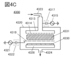
- 4A to 4C are cross-sectional views illustrating a film forming apparatus.
- FIG. 5 is a cross-sectional view illustrating a film forming apparatus.
- 6A to 6D are cross-sectional views illustrating an example of a method for manufacturing an oxide semiconductor.
- 7A to 7D are cross-sectional views illustrating an example of an oxide semiconductor.
- 8A to 8E are cross-sectional views illustrating a method for forming a metal oxide film according to one embodiment of the present invention.
- FIGS. 9A to 9D are cross-sectional views of a metal oxide according to one embodiment of the present invention.
- 10A to 10D are cross-sectional views illustrating a method for forming a metal oxide film according to one embodiment of the present invention.
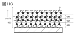
- 11A to 11C are cross-sectional views illustrating a method for forming a metal oxide film according to one embodiment of the present invention.
- Fig. 12A is a plan view showing an example of a semiconductor device
- Fig. 12B and Fig. 12C are cross-sectional views showing an example of the semiconductor device.
- FIG. 13 is a cross-sectional view showing an example of a semiconductor device.
- 14A and 14B are cross-sectional views showing an example of a semiconductor device.
- FIG. 15A is a plan view showing an example of a semiconductor device
- Fig. 15B and Fig. 15C are cross-sectional views showing an example of the semiconductor device.
- 16A and 16B are plan and cross-sectional views illustrating an example of a semiconductor device.
- 17A and 17B are plan and cross-sectional views illustrating an example of a semiconductor device.
- 18A to 18C are cross-sectional views showing an example of a semiconductor device.
- Fig. 19A is a plan view showing an example of a semiconductor device
- Fig. 19B and Fig. 19C are cross-sectional views showing an example of the semiconductor device.
- Fig. 20A is a plan view showing an example of a semiconductor device
- FIG. 20C are cross-sectional views showing an example of the semiconductor device.
- 21A to 21C are cross-sectional views showing an example of a method for manufacturing a semiconductor device.
- Fig. 22A is a plan view showing an example of a storage device
- Fig. 22B and Fig. 22C are cross-sectional views showing an example of the storage device.
- 23A and 23B are cross-sectional views showing an example of a memory device.
- 24A is a plan view of an example of a storage device
- FIG 24B is a cross-sectional view of the example of the storage device.
- FIG. 25 is a cross-sectional view showing an example of a storage device.
- FIG. 26 is a cross-sectional view showing an example of a storage device.
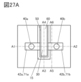
- FIG. 27A is a plan view showing an example of a semiconductor device
- Fig. 27B to Fig. 27D are cross-sectional views showing an example of the semiconductor device
- 28A and 28B are cross-sectional views showing an example of a semiconductor device.
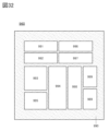
- FIG. 29 is a block diagram illustrating a configuration example of a semiconductor device.
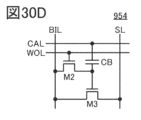
- 30A to 30H are diagrams for explaining examples of the circuit configuration of a memory cell.
- 31A and 31B are perspective views illustrating a configuration example of a semiconductor device.
- FIG. 32 is a block diagram illustrating the CPU.
- 33A and 33B are perspective views of a semiconductor device.
- 34A and 34B are perspective views of a semiconductor device.
- 35A and 35B are diagrams showing various storage devices by hierarchical level.
- FIG. 36A and 36B are perspective views showing an example of a display device.
- FIG. 37 is a cross-sectional view showing an example of a display device.
- FIG. 38 is a cross-sectional view showing an example of a display device.
- 39A to 39C are diagrams showing configuration examples of a display device.
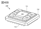
- 40A and 40B are diagrams showing an example of an electronic component.
- Fig. 41A to Fig. 41C are diagrams showing an example of a mainframe computer
- Fig. 41D is a diagram showing an example of space equipment
- Fig. 41E is a diagram showing an example of a storage system applicable to a data center.
- 42A to 42F are diagrams showing an example of an electronic device.
- 43A to 43G are diagrams showing an example of an electronic device.
- 44A to 44F are diagrams showing an example of an electronic device.
- ordinal numbers “first” and “second” are used for convenience and do not limit the number of components or the order of the components (e.g., process order or stacking order).
- an ordinal number attached to a component in one place in this specification may not match an ordinal number attached to the same component in another place in this specification or in the claims.
- a transistor is a type of semiconductor element that can perform functions such as amplifying current or voltage, and switching operations that control conduction or non-conduction.
- transistor includes IGFETs (Insulated Gate Field Effect Transistors) and thin film transistors (TFTs).
- a transistor that uses an oxide semiconductor or a metal oxide in a semiconductor layer and a transistor that has an oxide semiconductor or a metal oxide in a channel formation region may be referred to as an OS transistor.
- a transistor that has silicon in a channel formation region may be referred to as a Si transistor.
- a transistor is an element having at least three terminals including a gate, a drain, and a source.
- a transistor has a region (also called a channel formation region) where a channel is formed between the drain (drain terminal, drain region, or drain electrode) and the source (source terminal, source region, or source electrode), and a current can flow between the source and drain through the channel formation region.
- a channel formation region refers to a region through which a current mainly flows.
- source and drain may be interchangeable when transistors of different polarity are used, or when the direction of current changes during circuit operation. For this reason, in this specification, the terms “source” and “drain” can be used interchangeably.
- the impurity of a semiconductor refers to, for example, anything other than the main component constituting the semiconductor.
- an element with a concentration of less than 0.1 atomic % can be said to be an impurity.
- the defect level density of the semiconductor may increase or the crystallinity may decrease.
- the semiconductor is an oxide semiconductor
- examples of the impurity that changes the characteristics of the semiconductor include, for example, a Group 1 element, a Group 2 element, a Group 13 element, a Group 14 element, a Group 15 element, and a transition metal other than the main component of the oxide semiconductor.
- Specific examples of the impurity include, for example, hydrogen, lithium, sodium, silicon, boron, phosphorus, carbon, and nitrogen.
- water may also function as an impurity.
- oxygen vacancies also referred to as V O
- V O oxygen vacancies
- an oxynitride refers to a material whose composition contains more oxygen than nitrogen.
- An oxynitride refers to a material whose composition contains more nitrogen than oxygen.
- SIMS secondary ion mass spectrometry
- XPS X-ray photoelectron spectroscopy
- SIMS is suitable when the content of the target element is high (e.g., 0.5 atomic% or more, or 1 atomic% or more).
- SIMS is suitable when the content of the target element is low (e.g., 0.5 atomic% or less, or 1 atomic% or less).
- film and “layer” can be interchanged depending on the circumstances.
- conductive layer can be changed to the term “conductive film.”
- insulating film can be changed to the term “insulating layer.”
- parallel refers to a state in which two straight lines are arranged at an angle of -10 degrees or more and 10 degrees or less. Therefore, it also includes cases in which the angle is -5 degrees or more and 5 degrees or less.
- substantially parallel refers to a state in which two straight lines are arranged at an angle of -20 degrees or more and 20 degrees or less.
- perpendicular refers to a state in which two straight lines are arranged at an angle of 80 degrees or more and 100 degrees or less. Therefore, it also includes cases in which the angle is 85 degrees or more and 95 degrees or less.
- substantially perpendicular refers to a state in which two straight lines are arranged at an angle of 70 degrees or more and 110 degrees or less.
- electrically connected includes cases where the connection is made via "something that has some kind of electrical action.”
- something that has some kind of electrical action is not particularly limited as long as it allows the transmission and reception of electrical signals between the connected objects.
- something that has some kind of electrical action includes electrodes or wiring, as well as switching elements such as transistors, resistive elements, coils, and other elements with various functions.
- the off-state current refers to leakage current between the source and drain when a transistor is in an off state (also referred to as a non-conducting state or a cut-off state).
- the off state refers to a state in which the voltage Vgs between the gate and source of an n-channel transistor is lower than the threshold voltage Vth (higher than Vth for a p-channel transistor).
- the normally-on characteristic refers to a state in which a channel exists and current flows through the transistor even when no voltage is applied to the gate.
- the normally-off characteristic refers to a state in which no current flows through the transistor when no potential is applied to the gate or when a ground potential is applied to the gate.
- the top surface shape of a certain component refers to the contour shape of the component when viewed from a planar view.
- a planar view refers to a view from the normal direction of the surface on which the component is formed, or the surface of the support (e.g., substrate) on which the component is formed.
- top surface shapes are approximately the same.
- this includes cases where the upper and lower layers are processed using the same mask pattern, or where a portion of the mask pattern is the same.
- the contours may not overlap, and the upper layer may be located inside the lower layer, or outside the lower layer, in which case it may also be said that "top surface shapes are approximately the same.”
- the edges are aligned or approximately aligned, or that the side edges are aligned or approximately aligned.
- a tapered shape refers to a shape in which at least a portion of the side of the structure is inclined with respect to the substrate surface or the surface to be formed.
- the side of the structure, the substrate surface, and the surface to be formed do not necessarily need to be completely flat, and may be approximately planar with a slight curvature, or approximately planar with fine irregularities.
- A covers B
- at least a part of A covers B. Therefore, for example, it can be rephrased as saying that A has an area that covers B.
- a device fabricated using a metal mask or an FMM may be referred to as a device with an MM (metal mask) structure.
- a device fabricated without using a metal mask or an FMM may be referred to as a device with an MML (metal maskless) structure.
- SBS Side By Side
- the SBS structure allows the materials and configuration to be optimized for each light-emitting element, increasing the freedom of material and configuration selection and making it easier to improve brightness and reliability.
- holes or electrons may be referred to as "carriers".
- the hole injection layer or electron injection layer may be referred to as the "carrier injection layer”
- the hole transport layer or electron transport layer may be referred to as the “carrier transport layer”
- the hole block layer or electron block layer may be referred to as the "carrier block layer”.
- the above-mentioned carrier injection layer, carrier transport layer, and carrier block layer may not be clearly distinguishable.
- one layer may have two or three functions among the carrier injection layer, carrier transport layer, and carrier block layer.
- the light-emitting element has an EL layer between a pair of electrodes.
- the EL layer has at least a light-emitting layer.
- the layers (also called functional layers) that the EL layer has include a light-emitting layer, a carrier injection layer (hole injection layer and electron injection layer), a carrier transport layer (hole transport layer and electron transport layer), and a carrier block layer (hole block layer and electron block layer).
- the light-receiving element also called a light-receiving device
- one of the pair of electrodes may be referred to as a pixel electrode, and the other as a common electrode.
- the sacrificial layer (which may also be referred to as a mask layer) is located at least above the light-emitting layer (more specifically, the layer that is processed into an island shape among the layers that make up the EL layer) and has the function of protecting the light-emitting layer during the manufacturing process.
- an island-like EL layer refers to a state in which the EL layer is physically separated from the adjacent EL layer.
- step discontinuity refers to the phenomenon in which a layer, film, or electrode is separated due to the shape of the surface on which it is formed (e.g., a step, etc.).
- arrows indicating the X direction, Y direction, and Z direction may be used.
- the "X direction” is the direction along the X axis, and unless explicitly stated, no distinction is made between the forward direction and the reverse direction. The same applies to the "Y direction” and "Z direction.”
- the X direction, Y direction, and Z direction are directions that intersect with each other.
- the X direction, Y direction, and Z direction are directions that are perpendicular to each other.
- the oxide semiconductor layer according to one embodiment of the present invention is preferably used as a semiconductor layer of a transistor.
- the oxide semiconductor layer preferably has a channel formation region.
- the oxide semiconductor layer preferably has a source region and a drain region.
- the oxide semiconductor layer of one embodiment of the present invention preferably includes a metal oxide having crystallinity.
- a metal oxide having crystallinity examples include a c-axis aligned crystal (CAAC) structure, a polycrystalline (poly-crystal) structure, and a nanocrystalline (nc) structure.
- CAAC c-axis aligned crystal
- nc nanocrystalline
- the oxide semiconductor layer of one embodiment of the present invention preferably has a metal oxide having a CAAC structure.
- the CAAC structure is a crystal structure in which multiple microcrystals (typically multiple microcrystals having a hexagonal crystal structure) have a c-axis orientation and are connected without being oriented in the a-b plane.
- TEM transmission electron microscope
- the polycrystalline structure has grain boundaries.
- a minute gap also called a nanocrack or microcrack
- a minute space also called a nanospace or microspace
- the electrical resistance of the oxide semiconductor layer increases. This is because the electrical resistance of the minute gap or minute space is very high, for example, infinite.
- an oxide semiconductor layer having a minute gap or minute space is used in the channel formation region of a transistor, the contact resistance between the oxide semiconductor layer and one or both of the source electrode and the drain electrode increases. This adversely affects the initial characteristics or reliability of the transistor.
- the crystallinity of the oxide semiconductor layer can be analyzed, for example, by X-ray diffraction (XRD), TEM, or electron diffraction (ED). Alternatively, the analysis may be performed by combining a plurality of these techniques.
- XRD X-ray diffraction
- TEM TEM
- ED electron diffraction
- the crystallinity of the semiconductor material of the oxide semiconductor layer is not particularly limited.
- the oxide semiconductor layer may contain one or more of an amorphous semiconductor (a semiconductor having an amorphous structure), a single crystal semiconductor (a semiconductor having a single crystal structure), or a semiconductor having crystallinity other than single crystal (a microcrystalline semiconductor, a polycrystalline semiconductor, or a semiconductor having a crystalline region in part).
- an amorphous semiconductor a semiconductor having an amorphous structure
- a single crystal semiconductor a semiconductor having a single crystal structure
- a semiconductor having crystallinity other than single crystal a microcrystalline semiconductor, a polycrystalline semiconductor, or a semiconductor having a crystalline region in part.
- Examples of the metal oxide contained in the oxide semiconductor layer of one embodiment of the present invention include indium oxide, gallium oxide, and zinc oxide.
- the metal oxide according to one embodiment of the present invention preferably contains at least indium (In) or zinc (Zn).
- the metal oxide preferably contains two or three elements selected from indium, element M, and zinc.
- element M is a metal element or semimetal element having a high bond energy with oxygen, for example, a metal element or semimetal element having a bond energy with oxygen higher than that of indium.
- element M examples include aluminum, gallium, tin, yttrium, titanium, vanadium, chromium, manganese, iron, cobalt, nickel, zirconium, molybdenum, hafnium, tantalum, tungsten, lanthanum, cerium, neodymium, magnesium, calcium, strontium, barium, boron, silicon, germanium, and antimony.
- the element M of the metal oxide is preferably one or more of the above elements, more preferably one or more selected from aluminum, gallium, tin, and yttrium, and even more preferably gallium.
- the metal oxide according to one embodiment of the present invention preferably has one or more selected from indium, gallium, and zinc.
- metal elements and metalloid elements may be collectively referred to as “metal elements", and the "metal element” described in this specification may include metalloid elements.
- Metal oxides according to one embodiment of the present invention include, for example, indium zinc oxide (In-Zn oxide), indium tin oxide (In-Sn oxide), indium titanium oxide (In-Ti oxide), indium gallium oxide (In-Ga oxide), indium gallium aluminum oxide (In-Ga-Al oxide), indium gallium tin oxide (In-Ga-Sn oxide, also referred to as IGTO), gallium zinc oxide (Ga-Zn oxide, also referred to as GZO), aluminum zinc oxide (Al-Zn oxide, also referred to as AZO), indium aluminum
- the usable materials include indium zinc oxide (In-Al-Zn oxide, also referred to as IAZO), indium tin zinc oxide (In-Sn-Zn oxide, also referred to as ITZO (registered trademark)), indium titanium zinc oxide (In-Ti-Zn oxide), indium gallium zinc oxide (In-Ga-Zn oxide, also referred to as IGZO), in
- the transistor By increasing the ratio of the number of indium atoms to the total number of atoms of all metal elements contained in the metal oxide, the transistor can obtain a large on-current and high frequency characteristics.
- the metal oxide may have one or more kinds of metal elements having a higher period number in the periodic table instead of indium.
- the metal oxide may have one or more kinds of metal elements having a higher period number in the periodic table in addition to indium.
- Examples of metal elements having a higher period number in the periodic table include metal elements belonging to the fifth period and metal elements belonging to the sixth period.
- the metal elements include yttrium, zirconium, silver, cadmium, tin, antimony, barium, lead, bismuth, lanthanum, cerium, praseodymium, neodymium, promethium, samarium, and europium.
- Lanthanum, cerium, praseodymium, neodymium, promethium, samarium, and europium are called light rare earth elements.
- the metal oxide may also contain one or more nonmetallic elements.
- the field effect mobility of the transistor may be increased.
- nonmetallic elements include carbon, nitrogen, phosphorus, sulfur, selenium, fluorine, chlorine, bromine, and hydrogen.
- the metal oxide becomes highly crystalline, and the diffusion of impurities in the metal oxide can be suppressed. This suppresses fluctuations in the electrical characteristics of the transistor, and increases its reliability.
- the formation of oxygen vacancies in the metal oxide can be suppressed. Therefore, carrier generation caused by oxygen vacancies is suppressed, and a transistor with a small off-current can be obtained. In addition, fluctuations in the electrical characteristics of the transistor can be suppressed, and reliability can be improved.
- In-Ga-Zn oxide may be used as an example of a metal oxide.
- the oxide semiconductor layer of one embodiment of the present invention can be manufactured by forming a metal oxide using two types of film formation methods.
- the oxide semiconductor layer of one embodiment of the present invention can be manufactured by forming a metal oxide using a first film formation method and a second film formation method.
- a hybrid OS an oxide semiconductor layer formed using two types of film formation methods may be called a hybrid OS.
- the oxide semiconductor layer of one embodiment of the present invention has crystallinity.
- the oxide semiconductor layer of one embodiment of the present invention preferably has a CAAC structure.
- a metal oxide film having crystallinity is formed by using the first film formation method.
- the metal oxide film formed at this time has a CAAC structure.
- a metal oxide film formed by using a sputtering method is likely to have crystallinity.
- a mixed layer may be formed at the interface between the metal oxide and the layer on which it is formed.
- the mixed layer may be formed by particles (also called sputtering particles) emitted from a target or the like, or by energy imparted to the substrate by the sputtering particles or the like. There is a concern that the mixed layer may hinder the crystallization of the metal oxide.
- an insulating layer having silicon is used as the surface to be formed, such as silicon oxide
- silicon oxide there is a risk that silicon may be mixed into the metal oxide when a metal oxide is formed on the silicon oxide using the first film formation method.
- the crystallization of the metal oxide may be inhibited due to the mixing of impurities such as silicon into the metal oxide.
- a metal oxide is formed using the second film formation method. That is, after forming a metal oxide as a first layer using the second film formation method, a metal oxide is formed as a second layer on the first layer using the first film formation method. At this time, it is preferable to use a film formation method that causes less damage to the surface to be formed compared to the first film formation method as the second film formation method. By using a film formation method that causes less damage to the surface to be formed as the second film formation method, it is possible to suppress the formation of a mixed layer at the interface between the oxide semiconductor layer and the layer that is the surface to be formed of the oxide semiconductor layer.
- atomic layer deposition ALD
- chemical vapor deposition CVD
- a metal oxide having a microcrystalline structure or an amorphous structure with lower crystallinity than a CAAC structure may be formed as the first layer.
- the crystallinity of the first layer may be increased with the second layer as a nucleus. This may increase the crystallinity of the entire oxide semiconductor layer, including the vicinity of the interface with the surface on which it is formed.
- the oxide semiconductor layer of the present invention it is preferable to first form a metal oxide on a surface to be formed by using the second film formation method, and then form a metal oxide above the metal oxide by using the first film formation method.
- Examples of the first film formation method include sputtering and pulsed laser deposition (PLD).
- Examples of the second film formation method include the ALD method, plasma enhanced CVD (PECVD), thermal CVD, photo-CVD, metal organic CVD (MOCVD), and molecular beam epitaxy (MBE).
- the MBE method is a film formation method that grows a thin film with a crystal structure that reflects the crystal system of the substrate, and can be said to be one of the film formation methods that cause less damage to the surface on which the film is formed.
- a wet method can be used as the second film formation method.
- the wet method is one of the film formation methods that cause less damage to the surface on which the film is formed.
- An example of a wet method is the spray coating method.
- the oxide semiconductor layer of one embodiment of the present invention can be manufactured by forming a metal oxide as a first layer by using the second film formation method, and then forming a metal oxide as a second layer by using the first film formation method.
- the ALD method can be used as the second film formation method
- the sputtering method can be used as the first film formation method.
- the metal oxide formed by using the first film formation method preferably has a CAAC structure.
- a third layer can be formed on the second layer. Since the second layer has high crystallinity, the third layer can grow crystals using the crystals of the second layer as nuclei or seeds. Therefore, even if a film formation method that is likely to have crystallinity is not used as a film formation method for the third layer, the third layer can be crystallized.
- the oxide semiconductor layer can have both high crystallinity and high coverage throughout the entire layer.
- damage to the second layer is reduced, and the oxide semiconductor layer can have high crystallinity throughout the entire layer.
- the second layer has excellent crystallinity because the effect of the surface on which it is formed is reduced by providing the first layer, which increases its crystallinity. Therefore, it is expected that a layer with excellent crystallinity will also be formed in the third layer, which is crystallized using the second layer as a nucleus or seed.
- the third layer is the top layer of the oxide semiconductor layer, and is, for example, a layer in contact with the gate insulating layer when the oxide semiconductor layer is used as a semiconductor layer of a transistor described later.
- the oxide semiconductor layer of one embodiment of the present invention can be manufactured by forming a metal oxide as a first layer using the second film formation method, forming a metal oxide as a second layer using the first film formation method, and forming a metal oxide as a third layer using the second film formation method.
- the ALD method can be used as the second film formation method
- the sputtering method can be used as the first film formation method.
- the metal oxide formed using the first film formation method preferably has a CAAC structure.
- the ALD method is a film formation method with better coverage than the sputtering method, and the coverage of the oxide semiconductor layer can be improved by using the ALD method as the film formation method for the first layer and the third layer. Therefore, the oxide semiconductor layer can be well covered on steps, openings, etc. with high aspect ratios.
- Sputtering methods include RF sputtering, which uses a high-frequency power supply as the sputtering power source, DC sputtering, which uses a direct current power supply, and pulsed DC sputtering, which changes the voltage applied to the electrodes in a pulsed manner.
- RF sputtering is mainly used when depositing insulating films
- DC sputtering is mainly used when depositing metal conductive films.
- Pulsed DC sputtering is mainly used when depositing compounds such as oxides, nitrides, and carbides using the reactive sputtering method.
- Examples of the ALD method include the Thermal ALD method, in which the reaction between the precursor and reactant is carried out using only thermal energy, and the Plasma Enhanced ALD (PEALD) method, in which a plasma-excited reactant is used.
- Thermal ALD method in which the reaction between the precursor and reactant is carried out using only thermal energy
- PEALD Plasma Enhanced ALD
- the ALD method can deposit atoms one layer at a time, and therefore has the following advantages: extremely thin films can be formed; films can be formed on structures with high aspect ratios or surfaces with large steps; films can be formed with few defects such as pinholes; films can be formed with excellent coverage; and films can be formed at low temperatures.
- the PEALD method may be preferable because it uses plasma, which allows films to be formed at lower temperatures.
- some precursors used in the ALD method contain elements such as carbon or chlorine.
- films formed by the ALD method may contain more elements such as carbon or chlorine than films formed by other film formation methods. Note that the quantification of these elements can be performed using XPS or SIMS.
- the metal oxide film formation method of one embodiment of the present invention uses the ALD method, but adopts one or both of the conditions of a high substrate temperature during film formation and the implementation of an impurity removal process, so that the amount of carbon and chlorine contained in the film may be smaller than when the ALD method is used without applying these.
- the ALD method differs from other film-forming methods in that particles released from a target or the like are deposited, in that a film is formed by a reaction on the surface of the workpiece. Therefore, it is a film-forming method that is less affected by the shape of the workpiece and has good step coverage.
- the ALD method has excellent step coverage and excellent thickness uniformity, making it suitable for coating the surface of an opening with a high aspect ratio.
- the PECVD method can produce high-quality films at relatively low temperatures.
- the thermal CVD method does not use plasma, it is a film formation method that can reduce plasma damage to the workpiece.
- the thermal CVD method does not cause plasma damage during film formation, it can produce films with fewer defects.
- a film of any composition can be formed by changing the flow rate ratio of the raw material gases.
- a film with a continuously changing composition can be formed by changing the flow rate ratio of the raw material gases while forming the film.
- the oxide semiconductor layer 230 can be manufactured, for example, by forming an oxide semiconductor layer 230a over a layer 229 that is a surface to be formed by an ALD method, forming an oxide semiconductor layer 230b over the oxide semiconductor layer 230a by a sputtering method, and forming an oxide semiconductor layer 230c over the oxide semiconductor layer 230b by an ALD method.
- heat treatment is preferably performed. The heat treatment can improve the crystallinity of the oxide semiconductor layer 230.
- the heat treatment here is not limited to heat treatment. For example, heat applied during a manufacturing process may be used.
- the layer 229 is an insulating film, and is, for example, an insulating film of silicon oxide, silicon oxynitride, silicon nitride, silicon nitride oxide, aluminum oxide, hafnium oxide, or the like.
- a film to be described later as an insulator included in a semiconductor device can be used.
- layer 229 may be a conductive film.
- oxide semiconductor layer 230 may be formed on a conductive film that functions as an electrode of a semiconductor device.
- Layer 229 does not have to be crystalline. In other words, layer 229 may have an amorphous structure. Furthermore, if layer 229 has crystallinity, it may have a crystal structure with low lattice matching with the metal oxide of oxide semiconductor layer 230.
- an oxide semiconductor layer 230a is formed on the layer 229 (FIG. 6A). Then, an oxide semiconductor layer 230b is formed on the oxide semiconductor layer 230a (FIG. 6B).
- the oxide semiconductor layer 230b is preferably formed by using a sputtering method.
- the oxide semiconductor layer 230b preferably has a composition suitable for forming a CAAC structure.
- the oxide semiconductor layer 230a is formed using a deposition method that causes less damage to the surface on which it is formed compared to the deposition method for the oxide semiconductor layer 230b.
- the oxide semiconductor layer 230a is formed using the ALD method.
- an oxide semiconductor layer 230b is formed by a sputtering method.
- the oxide semiconductor layer 230a is preferably formed by a deposition method that causes little damage to a surface on which the oxide semiconductor layer 230a is to be formed.
- the oxide semiconductor layer 230a between the oxide semiconductor layer 230b and the layer 229 by a deposition method that causes little damage to a surface on which the oxide semiconductor layer 230a is to be formed, alloying between a component contained in the oxide semiconductor layer 230 and a component contained in the layer 229 can be suppressed, and the crystallinity of the oxide semiconductor layer 230 can be further improved.
- the thickness of the alloyed region can be made thin, or can be made thin enough that the alloyed region cannot be observed.
- the thickness of the alloyed region can be made 0 nm or more and 3 nm or less, preferably 0 nm or more and 2 nm or less, more preferably 0 nm or more and 1 nm or less, and even more preferably 0 nm or more and less than 0.3 nm.
- Figures 6A and 6B show an example in which no alloyed region is formed between layer 229 and oxide semiconductor layer 230a.
- the thickness of the alloyed region may be calculated by performing a line analysis of the composition of the region and its surroundings using SIMS or Energy Dispersive X-ray Spectroscopy (EDX).
- an EDX line analysis is performed on the above region and its periphery with the direction perpendicular to the surface of the oxide semiconductor layer 230a being the depth direction.
- the depth at which the quantitative value of a metal (In when the oxide semiconductor layer 230a contains In) that is the main component of the oxide semiconductor layer 230a and is not the main component of the layer that will be the surface to be formed (here, layer 229) becomes half-value is defined as the depth (position) of the interface between the above region and the oxide semiconductor layer 230a.
- the depth at which the quantitative value of an element (e.g., Si) that is the main component of the layer that will be the surface to be formed and is not the main component of the oxide semiconductor layer 230a becomes half-value is defined as the depth (position) of the interface between the above region and the layer that will be the surface to be formed. From the above, the thickness of the alloyed region can be calculated.
- an element e.g., Si
- the thickness of the alloyed region when the thickness of the alloyed region is observed by EDX analysis, the thickness is, for example, 0 nm or more and 3 nm or less, preferably 0 nm or more and 2 nm or less, more preferably 0 nm or more and 1 nm or less, and even more preferably 0 nm or more and less than 0.3 nm.
- the interface is defined as a depth at which the silicon concentration becomes 50% of the maximum concentration of the layer 229, and the distance between the interface and the depth at which the silicon concentration decreases to 1.0 ⁇ 10 21 atoms/cm 3 , preferably 5.0 ⁇ 10 20 atoms/cm 3 , more preferably 1.0 ⁇ 10 20 atoms/cm 3 is defined as thickness t_s2.
- the thickness t_s2 is preferably 3 nm or less, more preferably 2 nm or less.
- the thickness of the alloyed region can be reduced, allowing thickness t_s2 to be set to a value within the above range.
- near the surface to be formed refers to, for example, a region that is more than 0 nm and not more than 3 nm, preferably more than 0 nm and not more than 2 nm, and more preferably 1 nm or more and not more than 2 nm, approximately perpendicular to the surface to be formed of the oxide semiconductor layer 230.
- the CAAC structure near the surface to be formed can sometimes be confirmed by observation using a TEM.
- a TEM for example, in cross-sectional observation of the oxide semiconductor layer 230 using a high-resolution TEM, bright spots arranged in layers in a direction parallel to the surface to be formed can be confirmed near the surface to be formed.
- the CAAC structure near the surface to be formed may be evaluated from a map showing the crystal orientation.
- the map showing the crystal orientation may be obtained, for example, by acquiring a cross-sectional TEM image, performing a fast Fourier transform (FFT) process on each region in the cross-sectional TEM image to create an FFT pattern, and calculating the direction of the crystal axis of each region.
- the FFT pattern reflects reciprocal lattice space information similar to an electron diffraction pattern.
- a region in which the calculated crystal axis (c-axis) direction of each region is between 70° and 100° with respect to the surface to be formed can be considered to have a CAAC structure.
- an oxide semiconductor layer having a microcrystalline structure or an amorphous structure with lower crystallinity than the CAAC structure may be formed. That is, at the manufacturing stage shown in FIG. 6A, the oxide semiconductor layer 230a may have a region with lower crystallinity than the oxide semiconductor layer 230b.
- a source gas containing a precursor having indium is introduced into the chamber, and the precursor is adsorbed onto the surface of layer 229.
- the temperature for heating the substrate corresponds to the decomposition temperature of the precursor.
- the introduction of the raw material gas is stopped, the chamber is purged, and excess precursors and reaction products are discharged from the chamber.
- an oxidizing agent is introduced into the chamber as a reactant, and reacted with the adsorbed precursor, leaving indium adsorbed on the substrate while components other than indium are desorbed, forming a layer of indium and oxygen combined (hereinafter, the first layer). Ozone, oxygen, water, etc. can be used as the oxidizing agent.
- the introduction of the oxidizing agent is stopped, the chamber is purged, and excess reactants and reaction products are discharged from the chamber.
- a source gas containing a precursor having element M is introduced into the chamber and adsorbed onto the first layer.
- the temperature for heating the substrate corresponds to the decomposition temperature of the precursor.
- the introduction of the raw material gas is stopped, the chamber is purged, and excess precursors and reaction products are discharged from the chamber.
- an oxidizing agent is introduced into the chamber as a reactant, and is reacted with the adsorbed precursor, leaving element M adsorbed on the substrate while components other than element M are desorbed, forming a layer in which element M and oxygen are combined (hereinafter, the second layer).
- the introduction of the oxidizing agent is stopped, the chamber is purged, and excess reactants and reaction products are discharged from the chamber.
- a raw material gas containing a zinc-containing precursor is introduced into the chamber and adsorbed onto the second layer.
- the temperature for heating the substrate corresponds to the decomposition temperature of the precursor.
- the substrate heating temperature is 100°C or higher and 350°C or lower, preferably 150°C or higher and 300°C or lower.
- the introduction of the raw material gas is stopped, the chamber is purged, and excess precursors and reaction products are discharged from the chamber.
- an oxidizing agent is introduced into the chamber as a reactant, which reacts with the adsorbed precursor, leaving zinc adsorbed on the substrate while components other than zinc are desorbed, forming a layer of combined zinc and oxygen (hereinafter, the third layer).
- the introduction of the oxidizing agent is stopped, the chamber is purged, and excess reactants and reaction products are discharged from the chamber.
- the first layer is formed again on the third layer by the method described above.
- an In-M-Zn oxide can be formed as the oxide semiconductor layer 230a on the layer 229 by the ALD method.
- the ALD method can control the composition of the resulting film by adjusting the amount of source gas introduced.
- the ALD method can form a film of any composition by adjusting the amount of source gas introduced, the number of times it is introduced (also called the number of pulses), the time required for one pulse (also called the pulse time), and the like.
- the ALD method can form a film whose composition changes continuously by changing the source gas while forming the film.
- the time required for film formation can be shortened compared to forming a film using multiple film formation chambers because no time is required for transportation and pressure adjustment. Therefore, the productivity of semiconductor devices can be increased in some cases.
- an In-M-Zn oxide is formed as the oxide semiconductor layer 230b on the oxide semiconductor layer 230a using the sputtering method.
- the mixed layer 231 is formed on or near the surface of the oxide semiconductor layer 230a.
- minute crystal regions may be formed in the mixed layer 231 due to sputtering particles or energy provided to the substrate by the sputtering particles when the oxide semiconductor layer 230b is formed.
- the mixed layer 231 or the minute crystal regions formed in the mixed layer 231 may become nuclei, and at least a portion of the oxide semiconductor layer 230a may crystallize.
- In-Mn-Zn oxide can be used as a target for the sputtering method.
- oxygen or a mixture of oxygen and a noble gas can be used as the sputtering gas.
- the proportion of oxygen contained in the sputtering gas the amount of excess oxygen in the oxide film that is formed can be increased.
- the higher the ratio of the flow rate of oxygen gas to the total deposition gas used during deposition (hereinafter also referred to as the oxygen flow rate ratio), the more crystalline the metal oxide may be formed.
- an oxygen-excess metal oxide may be formed if the ratio of oxygen contained in the sputtering gas is set to more than 30% and not more than 100%, preferably 70% to 100%.
- a transistor using an oxygen-excess oxide semiconductor layer in a channel formation region can have relatively high reliability.
- one embodiment of the present invention is not limited to this.
- An oxygen-deficient metal oxide is formed if the ratio of oxygen contained in the sputtering gas is set to 1% to 30%, preferably 5% to 20%, in the film formation.
- a transistor using an oxygen-deficient metal oxide in a channel formation region can have relatively high field effect mobility.
- the composition of the formed metal oxide may differ from the composition of the sputtering target.
- the zinc content in the formed metal oxide may decrease to about 50% compared to the sputtering target.
- the substrate heating temperature is preferably, for example, 100°C or higher and 400°C or lower, and more preferably 200°C or higher and 300°C or lower.
- an oxide semiconductor layer 230a can be formed on layer 229, and an oxide semiconductor layer 230b can be formed on oxide semiconductor layer 230a.
- the oxide semiconductor layer 230c is formed on the oxide semiconductor layer 230b (FIG. 6C).
- the oxide semiconductor layer 230c is formed using the ALD method.
- the method for forming the oxide semiconductor layer 230a can be referred to.
- the oxide semiconductor layer 230c When an oxide semiconductor layer 230c having a lower crystallinity than the CAAC structure is formed on an oxide semiconductor layer 230b having a CAAC structure by using an ALD method, the oxide semiconductor layer 230c may grow epitaxially with the oxide semiconductor layer 230b as a nucleus. Therefore, when the oxide semiconductor layer 230c is formed, the oxide semiconductor layer 230c may have a region having the CAAC structure. In addition, it is preferable that the region having the CAAC structure is formed over the entire oxide semiconductor layer 230c.
- a heat treatment process may be performed.
- the temperature of the heat treatment may be, for example, 100°C to 800°C, preferably 250°C to 650°C, and more preferably 350°C to 550°C. Typically, the temperature can be 400°C ⁇ 25°C (375°C to 425°C).
- the treatment time can be 10 hours or less, or 1 minute to 5 hours, or 1 minute to 2 hours. When an RTA apparatus is used, the treatment time can be, for example, 1 second to 5 minutes. It is expected that the heat treatment will repair the gaps in the atomic level crystal parts of the CAAC structure of the oxide semiconductor layer 230b by the oxide semiconductor layer 230c (in other words, the crystal molecules formed by the ALD method).
- the heating device used for the heat treatment is not particularly limited, and may be a device that heats the workpiece by thermal conduction or thermal radiation from a heating element such as a resistance heating element.
- a heating element such as a resistance heating element.
- an electric furnace or an RTA (Rapid Thermal Anneal) device such as an LRTA (Lamp Rapid Thermal Anneal) device or a GRTA (Gas Rapid Thermal Anneal) device may be used.
- An LRTA device is a device that heats the workpiece by radiation of light (electromagnetic waves) emitted from lamps such as halogen lamps, metal halide lamps, xenon arc lamps, carbon arc lamps, high-pressure sodium lamps, and high-pressure mercury lamps.
- a GRTA device is a device that performs heat treatment using high-temperature gas.
- This heat treatment process may increase the crystallinity of the region having the CAAC structure in the oxide semiconductor layer 230c. Furthermore, if the region is formed only below the oxide semiconductor layer 230c after film formation by the ALD method, this heat treatment process may cause the region to expand upward (FIG. 6D). In other words, by performing this heat treatment, a region having the CAAC structure may be formed throughout the entire layer in the oxide semiconductor layer 230c.
- the heat treatment process may further repair the oxide semiconductor layer 230b by the oxide semiconductor layer 230c (in other words, the crystal molecules formed by the ALD method) that fills in the gaps in the atomic-level crystal parts of the CAAC structure of the oxide semiconductor layer 230b.
- the oxide semiconductor layer 230a is converted into CAAC by this heat treatment process (FIG. 6D). It is expected that the conversion into CAAC is facilitated by the mixed layer 231 formed in the oxide semiconductor layer 230a during the deposition of the oxide semiconductor layer 230b acting as a nucleus or seed. It is preferable that the region in the oxide semiconductor layer 230a that is converted into CAAC is large, and it is preferable that the conversion into CAAC extends to the vicinity of the layer 229.
- the CAAC is formed from the top to the bottom of the oxide semiconductor layer 230a, the CAAC can be formed up to the vicinity of the layer 229 without being limited by the material or crystallinity of the layer 229.
- the oxide semiconductor layer 230a can be formed with high crystallinity. Therefore, the method for manufacturing an oxide semiconductor layer according to one embodiment of the present invention is particularly suitable for the case where the layer on which the oxide semiconductor layer is to be formed has an amorphous structure.
- microwave treatment it is preferable to perform microwave treatment after the heat treatment step.
- the microwave treatment is preferably performed in an atmosphere containing oxygen. By performing microwave treatment, impurities such as hydrogen and carbon in the oxide semiconductor layer 230 can be reduced.
- the steps according to Figures 6A to 6D consecutively without exposing to the outside air.
- a multi-chamber manufacturing apparatus in which an ALD apparatus, a sputtering apparatus, and a heating apparatus are connected.
- an ALD apparatus a sputtering apparatus
- a heating apparatus By using such a multi-chamber manufacturing apparatus, it is possible to form and crystallize the oxide semiconductor layer 230 while suppressing the introduction of impurities.
- FIGS. 6A to 6D are cross-sectional views for explaining a method for forming a metal oxide film according to one embodiment of the present invention.
- FIGS. 6A to 6D can be regarded as conceptual diagrams showing a model for forming a metal oxide film according to one embodiment of the present invention.
- the oxide semiconductor layer 230a and the oxide semiconductor layer 230c each have high crystallinity using the oxide semiconductor layer 230b, which has high crystallinity, as a nucleus or seed.
- the crystallinity of the oxide semiconductor layer 230a may be increased by heat treatment during the formation of the oxide semiconductor layer 230b or after the formation of the oxide semiconductor layer 230c.
- the crystallinity of the oxide semiconductor layer 230c may be increased by heat treatment during the formation of the oxide semiconductor layer 230c or after the formation of the oxide semiconductor layer 230c.
- the heat treatment has an assisting effect for increasing the crystallinity.
- the highly crystalline oxide semiconductor layer 230b (i.e., CAAC) can be used as a nucleus or seed to increase the crystallinity of the upper and lower oxide semiconductors (here, the oxide semiconductor layer 230a and the oxide semiconductor layer 230c).
- CAAC the highly crystalline oxide semiconductor layer 230b
- the upper and lower oxide semiconductors can be grown in a solid phase using the oxide semiconductor layer 230b as a nucleus or seed to form a highly crystalline oxide semiconductor.
- the oxide semiconductor formed using such a film formation method, here a CAAC film can be referred to as an Axial Growth CAAC (AG CAAC).
- FIG. 7A shows the state in which the oxide semiconductor layer 230a, the oxide semiconductor layer 230b, and the oxide semiconductor layer 230c are each crystallized.
- the region having the CAAC structure is connected to the region having the CAAC structure in the oxide semiconductor layer 230b through crystals.
- the oxide semiconductor layer 230c the region having the CAAC structure is connected to the region having the CAAC structure in the oxide semiconductor layer 230b through crystals.
- the oxide semiconductor layer 230 may be expressed as a single layer whose interface is not clearly observed.
- the oxide semiconductor layer 230 may be expressed as a single layer.
- a part of the oxide semiconductor layer 230a or the oxide semiconductor layer 230c may not be crystallized. Also, a part of the oxide semiconductor layer 230a or the oxide semiconductor layer 230c may have a region with lower crystallinity than the CAAC structure remaining.
- the example shown in FIG. 7B shows a state in which the vicinity of the interface with the layer 229 in the oxide semiconductor layer 230a is not crystallized, or a region with lower crystallinity than the CAAC structure remains near the interface.
- FIG. 7C shows a state in which the vicinity of the surface in the oxide semiconductor layer 230c is not crystallized, or a region with lower crystallinity than the CAAC structure remains near the surface.
- FIG. 7D shows a state in which the vicinity of the interface of the oxide semiconductor layer 230a with the layer 229 and the vicinity of the surface of the oxide semiconductor layer 230c are not crystallized, or a region with lower crystallinity than the CAAC structure remains near the interface of the oxide semiconductor layer 230a with the layer 229 and near the surface of the oxide semiconductor layer 230c.
- the oxide semiconductor layer By increasing the crystallinity of the oxide semiconductor layer, it is expected that the increase in electrical resistance of the semiconductor layer of a transistor using the oxide semiconductor layer can be suppressed, or the initial characteristics (particularly the on-current) of the transistor can be improved, making the transistor suitable for high-speed operation. In addition, the reliability of the transistor can be increased, and the on-current can be increased.
- the method for manufacturing an oxide semiconductor layer according to one embodiment of the present invention can improve the crystallinity of metal oxides located above and below a metal oxide having a CAAC structure, making the entire oxide semiconductor layer into a highly crystalline layer.
- the oxide semiconductor layer of one embodiment of the present invention has high crystallinity throughout the layer. Therefore, in the oxide semiconductor layer 230, the boundaries between the stacked films of the oxide semiconductor layer 230a, the oxide semiconductor layer 230b, and the oxide semiconductor layer 230c may not be visible. In particular, after heat treatment, it may be difficult to confirm the boundaries between the stacked films. The presence or absence of boundaries between the stacked films can be confirmed by, for example, cross-sectional TEM, cross-sectional STEM, or the like.
- the field effect mobility of the transistor can be increased.
- an oxide semiconductor with a high In content tends to become polycrystalline.
- Using a metal oxide with a polycrystalline structure in a transistor adversely affects the initial characteristics or reliability of the transistor. Therefore, by using an oxide semiconductor with a high In content in one or both of the oxide semiconductor layer 230a and the oxide semiconductor layer 230c, crystals that reflect the crystal orientation of the oxide semiconductor layer 230b are formed, and polycrystallization can be suppressed.
- the degree of lattice mismatch between the crystals of the oxide semiconductor layer 230b and the crystals of the oxide semiconductor layer 230a or the oxide semiconductor layer 230c is small. This allows the oxide semiconductor layer 230a or the oxide semiconductor layer 230c to form crystals that reflect the orientation of the crystals of the oxide semiconductor layer 230b. At this time, for example, in cross-sectional observation of the oxide semiconductor layer 230 using a high-resolution TEM, bright spots arranged in layers in a direction parallel to the surface on which they are formed are confirmed in the oxide semiconductor layer 230a or the oxide semiconductor layer 230c.
- the crystal structure of the oxide semiconductor layer 230a or the oxide semiconductor layer 230c is not particularly limited.
- the crystal structure of the oxide semiconductor layer 230a or the oxide semiconductor layer 230c may be any of a cubic system, a tetragonal system, an orthorhombic system, a hexagonal system, a monoclinic system, and a trigonal system.
- the oxide semiconductor layer 230b preferably has a composition suitable for forming a CAAC structure.
- a sputtering method can be used to form the oxide semiconductor layer 230b.
- the oxide semiconductor layer 230b preferably contains zinc. By containing zinc, the oxide semiconductor layer 230b becomes a metal oxide with high crystallinity.
- the oxide semiconductor layer 230b preferably contains an element M in addition to zinc. By containing the element M in the oxide semiconductor layer 230b, for example, it is possible to suppress the formation of oxygen vacancies in the metal oxide. Therefore, the reliability of a transistor to which the oxide semiconductor layer is applied can be improved.
- the composition in the vicinity includes a range of ⁇ 30% of the desired atomic ratio.
- the oxide semiconductor layer 230b may be configured not to include the element M.
- it may be an In-Zn oxide.
- indium oxide may be used. It may also be configured to include a trace amount of the element M.
- the oxide semiconductor layer 230a and the oxide semiconductor layer 230c can be a metal oxide having a high ratio of In.
- the oxide semiconductor layer 230a and the oxide semiconductor layer 230c can be formed by, for example, the ALD method.
- a metal oxide having a high ratio of In it is possible to increase the on-current and improve the frequency characteristics when the oxide semiconductor layer is applied to a transistor.
- the oxide semiconductor layer 230a and the oxide semiconductor layer 230c may not contain the element M.
- they may be In-Zn oxide.
- indium oxide may be used.
- the oxide semiconductor layer 230a and the oxide semiconductor layer 230c may contain a trace amount of the element M.
- the oxide semiconductor layer 230a and the oxide semiconductor layer 230c can be made of a metal oxide having a higher proportion of In than the oxide semiconductor layer 230b.
- a metal oxide having a higher Ga ratio than the oxide semiconductor layer 230b can be used as the oxide semiconductor layer 230a and the oxide semiconductor layer 230c.
- the band gaps of the oxide semiconductor layer 230a and the oxide semiconductor layer 230c can be made larger than that of the oxide semiconductor layer 230b in some cases.
- the oxide semiconductor layer 230b is sandwiched between the oxide semiconductor layer 230a and the oxide semiconductor layer 230c, which have a larger band gap, and the oxide semiconductor layer 230b mainly functions as a current path (channel).
- the influence of the interface state that may be formed on the back channel side is reduced, and light deterioration of the transistor (e.g., negative bias light deterioration) can be suppressed, and the reliability of the transistor can be improved.
- the oxide semiconductor layer of one embodiment of the present invention can have a structure in which the entire oxide semiconductor layer including the oxide semiconductor layer 230a and the oxide semiconductor layer 230c has a CAAC structure because crystal growth occurs with the oxide semiconductor layer 230b as a nucleus.
- the CAAC structure can be formed in a region including at least a part of each of the oxide semiconductor layer 230a and the oxide semiconductor layer 230c and a region including the oxide semiconductor layer 230b.
- the oxide semiconductor layer 230a and the oxide semiconductor layer 230c have a composition with a high In content
- the oxide semiconductor layer can have a suitable crystallinity as a semiconductor layer of a transistor.
- oxide semiconductor layer 230a and oxide semiconductor layer 230c may be different.
- the oxide semiconductor layer 230a and the oxide semiconductor layer 230c may be made of a metal oxide having the same composition as the oxide semiconductor layer 230b. By using the same composition, CAAC formation may be more likely to occur after heat treatment.
- an oxide semiconductor layer having a CAAC structure formed using the above-mentioned two types of film formation methods may have a higher film relative dielectric constant, film density, and/or film hardness than an oxide semiconductor layer having a CAAC structure formed using one type of film formation method.
- an oxide semiconductor layer having a CAAC structure formed using the above-mentioned two types of film formation methods in the channel formation region of a transistor it is possible to realize a transistor with excellent characteristics (e.g., a transistor with a large on-state current, a transistor with high field-effect mobility, a transistor with a small S value, a transistor with high frequency characteristics (also called f characteristics), a highly reliable transistor, etc.).
- a transistor with excellent characteristics e.g., a transistor with a large on-state current, a transistor with high field-effect mobility, a transistor with a small S value, a transistor with high frequency characteristics (also called f characteristics), a highly reliable transistor, etc.
- the composition of the metal oxide used in the oxide semiconductor layer 230 can be analyzed using, for example, EDX, XPS, inductively coupled plasma mass spectrometry (ICP-MS), or inductively coupled plasma-atomic emission spectrometry (ICP-AES). Alternatively, the analysis may be performed by combining a plurality of these techniques. Note that for elements with low content, the actual content and the content obtained by analysis may differ due to the influence of analytical accuracy. For example, when the content of element M is low, the content of element M obtained by analysis may be lower than the actual content.
- the oxide semiconductor layer of one embodiment of the present invention can be used as a semiconductor layer of a transistor.
- the thickness of the oxide semiconductor layer 230 is, for example, preferably 3 nm or more and 200 nm or less, more preferably 3 nm or more and 100 nm or less, more preferably 5 nm or more and 100 nm or less, more preferably 10 nm or more and 100 nm or less, more preferably 10 nm or more and 70 nm or less, more preferably 15 nm or more and 70 nm or less, more preferably 15 nm or more and 50 nm or less, and more preferably 20 nm or more and 50 nm or less.
- the thickness of the oxide semiconductor layer 230 is preferably 1 nm or more, 3 nm or more, or 5 nm or more, and 20 nm or less, 15 nm or less, 12 nm or less, or 10 nm or less.
- the thickness of the oxide semiconductor layer 230b is preferably, for example, 200 nm or less. Furthermore, when the oxide semiconductor layer 230b is in a layered form, the thickness is preferably, for example, 1 nm or more and 200 nm or less, more preferably 1 nm or more and 100 nm or less, and more preferably 2 nm or more and 100 nm or less.
- the oxide semiconductor layer 230b can function as a crystal nucleus
- the oxide semiconductor layer 230b may not exist as a layer, but may be a collection of island-like regions. In such a case, for example, the island-like regions of the oxide semiconductor layer 230b exist discretely.
- the thickness of the oxide semiconductor layer 230a and the oxide semiconductor layer 230c is, for example, preferably 1 nm or more and 50 nm or less, more preferably 1 nm or more and 30 nm or less, more preferably 1 nm or more and 20 nm or less, and more preferably 2 nm or more and 20 nm or less.
- the oxide semiconductor layer of one embodiment of the present invention contains a metal oxide.
- Lattice defects include point defects such as atomic vacancies and foreign atoms, line defects such as dislocations, surface defects such as grain boundaries, and volume defects such as voids.
- Factors that cause lattice defects include a discrepancy in the ratio of the atomic numbers of the constituent elements (an excess or deficiency of constituent atoms) and impurities.
- the metal oxide used in the semiconductor layer of a transistor When a metal oxide is used in the semiconductor layer of a transistor, lattice defects in the metal oxide can cause carrier generation or capture. Therefore, if a metal oxide with many lattice defects is used in the semiconductor layer of a transistor, the electrical characteristics of the transistor may become unstable. Therefore, it is preferable that the metal oxide used in the semiconductor layer of a transistor has few lattice defects.
- the types of lattice defects likely to exist in metal oxides and the amount of lattice defects present vary depending on the structure of the metal oxide or the method of forming the metal oxide film.
- a metal oxide with high crystallinity for the semiconductor layer of a transistor.
- a metal oxide having a CAAC structure or a metal oxide having a single crystal structure By using such a metal oxide for a transistor, a transistor with good electrical characteristics can be realized. In addition, a highly reliable transistor can be realized.
- a metal oxide for the channel formation region of a transistor, which increases the on-state current of the transistor.
- the channel formation region of a transistor using an oxide semiconductor for the semiconductor layer has fewer oxygen vacancies or a lower concentration of impurities such as hydrogen, nitrogen, and metal elements than the source and drain regions.
- impurities such as hydrogen, nitrogen, and metal elements
- the electrical characteristics are likely to fluctuate and the reliability may be reduced.
- hydrogen near the oxygen vacancies may form defects in which hydrogen enters the oxygen vacancies (hereinafter, may be referred to as V O H), and may generate electrons that serve as carriers.
- V O H hydrogen near the oxygen vacancies
- the transistor is likely to have normally-on characteristics. Therefore, it is preferable that V O H is also reduced in the channel formation region.
- the channel formation region of the transistor is a high-resistance region with a low carrier concentration. Therefore, it can be said that the channel formation region of the transistor is i-type (intrinsic) or substantially i-type.
- impurities include hydrogen, carbon, and nitrogen.
- the impurities in the oxide semiconductor refer to, for example, elements other than the main components constituting the oxide semiconductor. For example, an element with a concentration of less than 0.1 atomic % can be considered an impurity.
- the carbon concentration in a channel formation region of the oxide semiconductor measured by SIMS is 1 ⁇ 10 20 atoms/cm 3 or less, preferably 5 ⁇ 10 19 atoms/cm 3 or less, more preferably 3 ⁇ 10 19 atoms/cm 3 or less, more preferably 1 ⁇ 10 19 atoms/cm 3 or less, more preferably 3 ⁇ 10 18 atoms/cm 3 or less, and further preferably 1 ⁇ 10 18 atoms/cm 3 or less.
- the silicon concentration in the channel formation region of the oxide semiconductor measured by SIMS is 1 ⁇ 10 20 atoms/cm 3 or less, preferably 5 ⁇ 10 19 atoms/cm 3 or less, more preferably 3 ⁇ 10 19 atoms/cm 3 or less, more preferably 1 ⁇ 10 19 atoms/cm 3 or less, more preferably 3 ⁇ 10 18 atoms/cm 3 or less, and still more preferably 1 ⁇ 10 18 atoms/cm 3 or less.
- the nitrogen concentration in a channel formation region of an oxide semiconductor obtained by SIMS is set to 1 ⁇ 10 20 atoms/cm 3 or less, preferably 5 ⁇ 10 19 atoms/cm 3 or less, more preferably 1 ⁇ 10 19 atoms/cm 3 or less, more preferably 5 ⁇ 10 18 atoms/cm 3 or less, more preferably 1 ⁇ 10 18 atoms/cm 3 or less, and further preferably 5 ⁇ 10 17 atoms/cm 3 or less.
- Hydrogen contained in the oxide semiconductor reacts with oxygen bonded to a metal atom to form water, which may form an oxygen vacancy.
- an electron serving as a carrier may be generated.
- some of the hydrogen may bond to oxygen bonded to a metal atom to generate an electron serving as a carrier. Therefore, a transistor using an oxide semiconductor containing hydrogen is likely to have normally-on characteristics. For this reason, it is preferable that hydrogen in a channel formation region of the oxide semiconductor is reduced as much as possible.
- the hydrogen concentration in the channel formation region of the oxide semiconductor obtained by SIMS is less than 1 ⁇ 10 20 atoms/cm 3 , preferably less than 5 ⁇ 10 19 atoms/cm 3 , more preferably less than 1 ⁇ 10 19 atoms/cm 3 , more preferably less than 5 ⁇ 10 18 atoms/cm 3 , more preferably less than 1 ⁇ 10 18 atoms/cm 3 , and further preferably less than 1 ⁇ 10 17 atoms/cm 3 .
- the concentration of the alkali metal or the alkaline earth metal in a channel formation region of the oxide semiconductor obtained by SIMS is set to 1 ⁇ 10 18 atoms/cm 3 or less, preferably 2 ⁇ 10 16 atoms/cm 3 or less.
- the oxide semiconductor layer of one embodiment of the present invention has a CAAC structure.
- the crystallinity of the oxide semiconductor layer of one embodiment of the present invention can be evaluated using crystal orientation, for example.
- Crystal orientation can be obtained from the Fast Fourier Transform (FFT) pattern by performing FFT processing on the TEM image. Specifically, the direction of the crystal axis can be obtained using the FFT pattern.
- the FFT pattern obtained by FFT processing reflects reciprocal lattice space information similar to that of an electron diffraction pattern.
- the crystal orientation of each region can be obtained. For example, by obtaining the crystal orientation of each region within a certain area, a map showing the crystal orientation can be formed. Specifically, two spots of high intensity are observed in the FFT pattern of a region having layered crystal parts. The direction of the crystal axis of the region can be obtained from the angle of the line segment connecting the two spots.
- the c-axis orientation rate can be calculated by calculating the percentage of c-axis oriented regions in a map showing crystal orientation. Note that c-axis oriented regions are defined here as regions whose orientation coincides with the c-axis and regions whose orientation differs from the c-axis by 20° or less.
- the c-axis orientation rate can be calculated, for example, by performing TEM observation of a cross section or a plan view of the oxide semiconductor layer.
- the region where FFT is performed (also referred to as an FFT window) can be, for example, a circle with a diameter of 1.0 nm. Note that the region where FFT is performed is not limited to a circle.
- the c-axis orientation rate is 60% or more, preferably 70% or more, more preferably 80% or more, more preferably 90% or more, and even more preferably 95% or more.
- the c-axis orientation rates of the region where the oxide semiconductor layer 230a is formed, the region where the oxide semiconductor layer 230b is formed, and the region where the oxide semiconductor layer 230c is formed are Rc1, Rc2, and Rc3, respectively.
- Rc2 is 60% or more, preferably 70% or more, more preferably 80% or more, more preferably 90% or more, and even more preferably 95% or more.
- Rc3 is 60% or more, preferably 70% or more, more preferably 80% or more, more preferably 90% or more, and even more preferably 95% or more.
- Rc3/Rc1 is preferably greater than 1.
- Rc2/Rc1 is preferably greater than 1.
- oxide semiconductor layer 230 is fabricated, the boundaries between the oxide semiconductor layers 230a, 230b, and 230c may not be clearly observed.
- the oxide semiconductor layer 230 of one embodiment of the present invention can be divided into three regions, a first region, a second region, and a third region, in this order from the top of the layer 229. Each region is a layered region.
- the first region, the second region, and the third region each have a CAAC structure. Furthermore, it is preferable that the c-axis orientation rate of the third region is higher than that of the first region. Furthermore, it is preferable that the c-axis orientation rate of the second region is higher than that of the first region. Furthermore, the c-axis orientation rate of the third region is 80% or more, more preferably 90% or more, and even more preferably 95% or more. Furthermore, the c-axis orientation rate of the second region is 80% or more, more preferably 90% or more, and even more preferably 95% or more.
- the first region is located at a distance of 0 nm to 3 nm from the top surface of layer 229, and the third region is located at a distance of 0 nm to 3 nm from the top surface of oxide semiconductor layer 230.
- the layer thicknesses of each region are approximately the same.
- a precursor 611a is introduced into a chamber, and the precursor 611a is adsorbed on the surface of a substrate 610 (see Fig. 8A.
- this process may be referred to as the first step).
- the precursor 611a is adsorbed on the surface of the substrate 610, and a self-termination mechanism of the surface chemical reaction is activated, so that the precursor 611a is not further adsorbed on the layer of the precursor 611a on the substrate 610.
- the appropriate range of the substrate temperature in which the self-termination mechanism of the surface chemical reaction is activated is also called the ALD window.
- the ALD window is determined by the temperature characteristics, vapor pressure, decomposition temperature, etc. of the precursor, and may be, for example, 100°C to 600°C, preferably 200°C to 400°C.
- an inert gas such as argon, helium, or nitrogen
- an inert gas is introduced into the chamber to discharge excess precursor 611a and reaction products from the chamber (hereinafter, this process may be referred to as the second step).
- excess precursor and reaction products may be discharged from the chamber by vacuum evacuation.
- the second step is also called purging.
- a reactant 612a for example, an oxidant (ozone ( O3 ), oxygen ( O2 ), water ( H2O ), and plasma, radicals, ions, etc.
- a reactant 612a for example, an oxidant (ozone ( O3 ), oxygen ( O2 ), water ( H2O ), and plasma, radicals, ions, etc.
- O3 oxidant
- O2 oxygen
- H2O water
- this process may be referred to as the third step).
- a layer of oxide 613a formed by oxidizing part of the precursor 611a is formed on the surface of the substrate 610.
- precursor 611b having a metal element different from precursor 611a is introduced, and a process similar to the first step is carried out to adsorb precursor 611b onto the surface of the layer of oxide 613a (see FIG. 8C).
- the precursor 611b is adsorbed onto the layer of oxide 613a, and a self-terminating mechanism for the surface chemical reaction is activated, so that precursor 611b is not further adsorbed onto the layer of precursor 611b on substrate 610.
- reactant 612b is introduced into the chamber.
- reactant 612b may be the same as reactant 612a or may be different (see FIG. 8D).
- a layer of oxide 613b which is formed by oxidizing a portion of precursor 611b, is formed on the layer of oxide 613a.
- a layer of oxide 613c can be formed on the layer of oxide 613b.
- a metal oxide having a layered crystal structure in which the stacked structure of oxides 613a to 613c is repeated can be formed (see FIG. 8E).
- a layer of oxide can be formed by performing the first to fourth steps as one set, and by repeating this set, a layered crystal structure in which multiple oxide layers are stacked can be formed.
- the thickness of the metal oxide with a layered crystal structure can be 1 nm or more and less than 100 nm, preferably 3 nm or more and less than 20 nm.
- the substrate temperature can be set to 100° C. or higher and 600° C. or lower, preferably 100° C. or higher and 350° C. or lower, and more preferably 200° C. or higher and lower than the decomposition temperature of the precursor.
- the substrate temperature is preferable to set the substrate temperature to a temperature lower than the decomposition temperature of the lowest precursor among the multiple precursors. This allows the multiple precursors used to be adsorbed onto the target (e.g., substrate) without being decomposed during film formation by the ALD method.
- impurities such as hydrogen or carbon contained in the precursor and reactant can be removed from the metal oxide in each process of steps 1 to 4.
- impurities such as hydrogen or carbon contained in the precursor and reactant
- carbon in the metal oxide can be released as CO2 and CO
- hydrogen in the metal oxide can be released as H2O .
- rearrangement of metal atoms and oxygen atoms can be performed, and each oxide layer can be arranged with high order. Therefore, a metal oxide with a highly crystalline layered crystal structure can be formed.
- the precursor used in the film formation has a high decomposition temperature.
- the decomposition temperature of the precursor is preferably 200°C or higher and 700°C or lower, and more preferably 250°C or higher and 600°C or lower.
- an inorganic precursor As a precursor with such a high decomposition temperature, it is preferable to use a precursor formed of an inorganic substance (hereinafter referred to as an inorganic precursor).
- Inorganic precursors generally tend to have a higher decomposition temperature than precursors formed of an organic substance (hereinafter referred to as an organic precursor), and some have an ALD window in the above temperature range.
- inorganic precursors do not contain impurities such as hydrogen or carbon, so it is possible to prevent an increase in the concentration of impurities such as hydrogen or carbon in the metal oxide film formed.
- heat treatment after the metal oxide film is formed.
- the heat treatment can be performed under the conditions described in Figures 6A to 6D, etc.
- impurities such as hydrogen or carbon contained in the metal oxide
- carbon in the metal oxide can be released as CO2 and CO
- hydrogen in the metal oxide can be released as H2O .
- rearrangement of metal atoms and oxygen atoms can be carried out, improving crystallinity. Therefore, a metal oxide with a highly crystalline layered crystal structure can be formed.
- microwave treatment in an atmosphere containing oxygen to reduce the impurity concentration in the metal oxide.
- impurities include, in particular, hydrogen and carbon.
- microwave treatment may be performed on an insulating film, more specifically, a silicon oxide film, located near the metal oxide in an atmosphere containing oxygen.
- FIG. 8 describes a structure in which the stacked structure of oxides 613a to 613c is repeated, the present invention is not limited to this.
- a metal oxide in which a single layer, two layers, or four or more oxide layers are repeatedly formed may be used.
- ozone, oxygen, or water are not limited to gaseous or molecular states, but also include plasma, radical, and ionic states.
- plasma, radical, and ionic states are not limited to gaseous or molecular states, but also include plasma, radical, and ionic states.
- the PEALD method may be used.
- the pulse time for introducing the oxidizing agent can be lengthened.
- the oxidizing agent can be introduced multiple times.
- the same type of oxidizing agent may be introduced, or different types of oxidizing agents may be introduced.
- water may be introduced into the chamber as the first oxidizing agent, followed by evacuation, and ozone or oxygen not containing hydrogen as the second oxidizing agent may be introduced into the chamber, followed by evacuation.
- the ALD method is a film formation method that uses thermal energy to react precursors and reactants.
- the temperature required for the reaction of the precursors and reactants is determined by their temperature characteristics, vapor pressure, decomposition temperature, etc., but is between 100°C and 600°C, preferably between 200°C and 600°C.
- the ALD method in which a plasma-excited reactant is introduced into the chamber as a third source gas is sometimes called the PEALD method.
- a plasma generating device is provided at the inlet for the third source gas.
- ICP Inductively Coupled Plasma
- the ALD method in which the precursor and reactant react using thermal energy is sometimes called the thermal ALD method.
- a plasma-excited reactant is introduced in the third step to form a film.
- the first to fourth steps are repeated and a plasma-excited reactant (second reactant) is introduced at the same time to form a film.
- the reactant introduced in the third step is called the first reactant.
- the second reactant used in the third raw material gas can be made of the same material as the oxidizing agent. That is, plasma-excited ozone, oxygen, and water can be used as the second reactant.
- a nitriding agent may be used as the second reactant. Nitrogen (N 2 ) or ammonia (NH 3 ) can be used as the nitriding agent.
- a mixed gas of nitrogen (N 2 ) and hydrogen (H 2 ) can be used as the nitriding agent.
- a mixed gas of 5% nitrogen (N 2 ) and 95% hydrogen (H 2 ) can be used as the nitriding agent.
- argon (Ar), helium (He) or nitrogen (N 2 ) may be used as the carrier gas of the second reactant.
- a carrier gas such as argon, helium or nitrogen
- nitrogen when forming an oxide film such as a metal oxide film using the PEALD method, if nitrogen is used as the carrier gas, nitrogen may be mixed into the film, and the desired film quality may not be obtained. In this case, it is preferable to use argon or helium as the carrier gas.
- the ALD method can deposit extremely thin films with uniform thickness. It also has a high surface coverage rate, even on uneven surfaces.
- FIG. 9A is a diagram showing an oxide 660 having an In-M-Zn oxide formed on a structure 650.
- the structure refers to an element that constitutes a semiconductor device such as a transistor.
- the structure 650 includes conductors such as a substrate, a gate electrode, a source electrode, and a drain electrode, insulators such as a gate insulating film, an interlayer insulating film, and a base insulating film, metal oxides, and semiconductors such as silicon.
- FIG. 9A shows a case where the surface of the structure 650 to be deposited is arranged parallel to the substrate (or base body, not shown).
- Fig. 9B is an enlarged view showing the atomic arrangement in a crystal in a region 653 which is a part of the oxide 660 in Fig. 9A.
- the element M is a metal element with a valence of +3.
- the crystals of oxide 660 are formed by repeatedly stacking a layer 621 having indium (In) and oxygen, a layer 631 having element M and oxygen, and a layer 641 having zinc (Zn) and oxygen, in that order.
- Layers 621, 631, and 641 are arranged approximately parallel to the deposition surface of structure 650. That is, the a-b plane of oxide 660 is approximately parallel to the deposition surface of structure 650, and the c-axis of oxide 660 is approximately parallel to the normal direction of the deposition surface of structure 650.
- each of layers 621, 631, and 641 of the crystal is composed of one metal element and oxygen, and is arranged with good crystallinity, which can increase the carrier mobility of the metal oxide.
- the order of stacking layers 621, 631, and 641 may be changed.
- layers 621, 641, and 631 may be repeatedly stacked in this order.
- layers 621, 631, 641, 621, 641, and 631 may be repeatedly stacked in this order.
- part of the element M in layer 631 may be replaced with zinc
- part of the zinc in layer 641 may be replaced with element M.
- FIG. 9C shows an oxide 662 having an In-M-Zn oxide formed on the structure 650.
- FIG. 9D shows an enlarged view of the atomic arrangement in the crystal in region 654, which is part of the oxide 662 in FIG. 9C.
- the crystals of oxide 662 include layer 622 having indium (In), element M, and oxygen, layer 641 having zinc (Zn) and oxygen, and layer 631 having element M and oxygen.
- oxide 662 multiple layers are repeatedly stacked in the order of layer 622, layer 641, layer 631, and layer 641.
- Layers 622, 631, and 641 are arranged approximately parallel to the deposition surface of structure 650.
- the a-b plane of oxide 662 is approximately parallel to the deposition surface of structure 650
- the c-axis of oxide 662 is approximately parallel to the normal direction of the deposition surface of structure 650.
- the stacking order of layers 622, 631, and 641 may be changed.
- part of the element M in layer 631 may be replaced with zinc, and part of the zinc in layer 641 may be replaced with element M.
- layer 621 or layer 631 may be formed instead of layer 622.
- a source gas containing an indium-containing precursor is introduced into the chamber, and the precursor is adsorbed onto the surface of the structure 650 (see FIG. 10A).
- the source gas contains a carrier gas such as argon, helium, or nitrogen in addition to the precursor.
- a carrier gas such as argon, helium, or nitrogen in addition to the precursor.
- a precursor containing indium trimethylindium, triethylindium, tris(2,2,6,6-tetramethyl-3,5-heptanedionate)indium, cyclopentadienylindium, indium(III) acetylacetonate, (3-(dimethylamino)propyl)dimethylindium, etc. can be used.
- an inorganic precursor that does not contain a hydrocarbon may be used as a precursor containing indium.
- a halogen-based indium compound such as indium trichloride, indium tribromide, or indium triiodide may be used as an inorganic precursor containing indium.
- Indium trichloride has a decomposition temperature of about 500°C to 700°C. Therefore, by using indium trichloride, a film can be formed by the ALD method while heating the substrate at about 400°C to 600°C, for example, at 500°C.
- the introduction of the source gas is stopped, the chamber is purged, and excess precursors and reaction products are discharged from the chamber.
- an oxidizing agent is introduced into the chamber as a reactant and reacted with the adsorbed precursor, and components other than indium are desorbed while indium remains adsorbed on the substrate, forming a layer 621 in which indium and oxygen are combined (see FIG. 10B).
- Ozone, oxygen, water, etc. can be used as the oxidizing agent.
- the introduction of the oxidizing agent is stopped, and the chamber is purged to discharge excess reactants and reaction products from the chamber.
- a source gas containing a precursor having element M is introduced into the chamber, and the precursor is adsorbed onto layer 621 (see FIG. 10C).
- the source gas contains a carrier gas such as argon, helium, or nitrogen.
- precursors having gallium can be trimethylgallium, triethylgallium, tris(dimethylamido)gallium, gallium(III) acetylacetonate, tris(2,2,6,6-tetramethyl-3,5-heptanedionate)gallium, dimethylchlorogallium, diethylchlorogallium, dimethylgallium isopropoxide, etc.
- inorganic precursors that do not contain hydrocarbons may be used as precursors containing gallium.
- Halogen-based gallium compounds such as gallium trichloride, gallium tribromide, and gallium triiodide can be used as inorganic precursors containing gallium.
- Gallium trichloride has a decomposition temperature of about 550°C to 700°C. Therefore, by using gallium trichloride, it is possible to form a film by the ALD method while heating the substrate at about 450°C to 650°C, for example, at 550°C.
- the introduction of the source gas is stopped, the chamber is purged, and excess precursors and reaction products are discharged from the chamber.
- an oxidizing agent is introduced into the chamber as a reactant and reacted with the adsorbed precursor, and components other than element M are desorbed while element M is still adsorbed on the substrate, forming layer 631 in which element M is combined with oxygen (see FIG. 10D). At this time, some of the oxygen constituting layer 641 may be adsorbed onto layer 631.
- the introduction of the oxidizing agent is stopped, and the chamber is purged to discharge excess reactant and reaction products from the chamber.
- a source gas containing a zinc-containing precursor is introduced into the chamber, and the precursor is adsorbed onto layer 631 (see FIG. 11A). At this time, a part of layer 641 in which zinc and oxygen are combined may be formed.
- the source gas contains a carrier gas such as argon, helium, or nitrogen. Examples of precursors that can be used that contain zinc include dimethylzinc, diethylzinc, zinc bis(2,2,6,6-tetramethyl-3,5-heptanedionate), and zinc acetate.
- inorganic precursors that do not contain hydrocarbons may be used as precursors containing zinc.
- Halogen-based zinc compounds such as zinc dichloride, zinc dibromide, and zinc diiodide can be used as inorganic precursors containing zinc.
- Zinc dichloride has a decomposition temperature of about 450°C to 700°C. Therefore, by using zinc dichloride, it is possible to form a film by the ALD method while heating the substrate at about 350°C to 550°C, for example, at 450°C.
- the introduction of the source gas is stopped, the chamber is purged, and excess precursors and reaction products are discharged from the chamber.
- an oxidizing agent is introduced into the chamber as a reactant and reacted with the adsorbed precursor, and components other than zinc are desorbed while zinc remains adsorbed on the substrate, forming a layer 641 in which zinc and oxygen are combined (see FIG. 11B).
- the introduction of the oxidizing agent is stopped, and the chamber is purged to discharge excess reactant and reaction products from the chamber.
- layer 621 is formed again on layer 641 by the method described above (see FIG. 11C).
- oxide 660 can be formed on the substrate or structure.
- Some of the above precursors contain carbon and/or chlorine in addition to metal elements. Films formed using precursors containing carbon may contain carbon. Films formed using precursors containing halogens such as chlorine may contain halogens such as chlorine.
- a metal oxide can be formed in which the c-axis is oriented approximately parallel to the normal direction of the deposition surface.
- layered crystals can be formed that are approximately parallel to the sidewall of the opening 290, particularly the side surface of the insulating layer 280. With this configuration, the layered crystals of the oxide semiconductor layer 230 are formed approximately parallel to the channel length direction of the transistor 200, so that the on-current of the transistor can be increased.
- the steps shown in Figures 10A to 11C are preferably performed while heating the substrate.
- the substrate temperature can be set to 100°C or higher and 600°C or lower, preferably 100°C or higher and 350°C or lower, and more preferably 200°C or higher and lower than the decomposition temperature of the precursor.
- the precursor used in the film formation has a high decomposition temperature.
- the decomposition temperature of the precursor is preferably 200°C or higher and 700°C or lower, and more preferably 250°C or higher and 600°C or lower.
- an inorganic precursor As a precursor with such a high decomposition temperature, it is preferable to use an inorganic precursor. Inorganic precursors generally tend to have a higher decomposition temperature than organic precursors, so the precursor is less likely to decompose even if film formation is performed while heating the substrate as described above.
- Inorganic precursors may be, for example, the above-mentioned indium trichloride, gallium trichloride, or zinc dichloride.
- the decomposition temperature of these precursors is about 350°C or higher and 700°C or lower, which is considerably higher than the decomposition temperature of general organic precursors.
- the decomposition temperatures of indium trichloride, gallium trichloride, and zinc dichloride are different from each other. In this way, when forming a film by the ALD method using multiple different types of precursors, it is preferable to set the substrate temperature to a temperature lower than the decomposition temperature of the lowest precursor among the multiple precursors.
- the substrate temperature can be set within a range in which zinc dichloride, which has the lowest decomposition temperature of the precursor, does not decompose. This allows other indium trichloride and gallium trichloride to be adsorbed onto the target (e.g., a substrate, etc.) without being decomposed.
- layer 621 is formed as a layer containing indium
- layer 631 is formed thereon as a layer containing element M
- layer 641 is further formed thereon as a layer containing zinc
- this embodiment is not limited to this.
- One of layer 631 and layer 641 may be formed, layer 621 may be formed thereon, and the other of layer 631 and layer 641 may be formed thereon.
- one of layer 631 and layer 641 may be formed, the other of layer 631 and layer 641 may be formed thereon, and layer 621 may be formed thereon.
- FIG. 1 is a schematic diagram of a multi-chamber type manufacturing apparatus 4000.
- FIG. 2 is a schematic diagram of a multi-chamber type manufacturing apparatus 4050.
- FIGS. 3A and 3B are cross-sectional views of an ALD apparatus that can be used in the manufacturing apparatus.
- FIGS. 4A to 4C are cross-sectional views of an ALD apparatus that can be used in the manufacturing apparatus.
- FIG. 5 is a cross-sectional view of a sputtering apparatus that can be used in the manufacturing apparatus. Note that FIGS. 1 to 5 show representative configurations, and some configurations are omitted.
- the manufacturing apparatus 4000 has a loading/unloading chamber 4002, a loading/unloading chamber 4004, a transfer chamber 4006, a film formation chamber 4008, a film formation chamber 4009, a film formation chamber 4010, and a processing chamber 4011.
- the loading/unloading chamber 4002 and the loading/unloading chamber 4004 have the function of switching the pressure in the chamber from atmospheric pressure to reduced pressure or from reduced pressure to atmospheric pressure, and can load or unload a substrate.
- the transfer chamber 4006 is provided with a transfer arm 4014, and can transport a substrate to each chamber in a vacuum.
- the loading/unloading chamber 4002, the loading/unloading chamber 4004, the film-forming chamber 4008, the film-forming chamber 4009, the film-forming chamber 4010, and the processing chamber 4011 are each connected to the transfer chamber 4006 via a gate valve. Therefore, the manufacturing apparatus 4000 can independently maintain a vacuum state in each chamber. This allows continuous processing to be performed in the film-forming chamber 4008, the film-forming chamber 4009, the film-forming chamber 4010, and the processing chamber 4011 without exposure to the atmosphere, and prevents impurities from being mixed into the film. In addition, contamination of the interface between the substrate and the film and the interface between each film is reduced, resulting in clean interfaces.
- An ALD device and a sputtering device can be used in the film formation chambers 4008 to 4010.
- an ALD device can be used in the film formation chambers 4008 and 4010, and a sputtering device can be used in the film formation chamber 4009.
- a heating device (typically, a vacuum heating device) can be used in the processing chamber 4011.
- the processing chamber 4011 can also be configured to include a processing device other than a film formation device, such as a plasma generation device (typically, a microwave processing device).
- the oxide semiconductor layer 230a according to FIG. 6A can be formed in the film formation chamber 4008 by using the ALD method. Furthermore, the oxide semiconductor layer 230b according to FIG. 6B can be formed in the film formation chamber 4009 by using the sputtering method. Furthermore, the oxide semiconductor layer 230c according to FIG. 6C can be formed in the film formation chamber 4010 by using the ALD method. Furthermore, the heat treatment according to FIG. 6D can be performed in the treatment chamber 4011.
- the oxide semiconductor layers 230a to 230c are continuously processed without being exposed to the air. This makes it possible to prevent impurities from being mixed into the formed oxide semiconductor layer 230. In addition, since the inhibition of crystal growth by impurities is suppressed, the crystallinity can be improved.
- the oxide semiconductor layer By increasing the crystallinity of the oxide semiconductor layer, it is expected that the increase in electrical resistance of the semiconductor layer of a transistor using the oxide semiconductor layer can be suppressed, or the initial characteristics (particularly the on-state current) of the transistor can be improved, making the transistor suitable for high-speed operation. In addition, the reliability of the transistor can be improved.
- the loading/unloading chamber 4002, the loading/unloading chamber 4004, the transfer chamber 4006, the film-forming chamber 4008, the film-forming chamber 4009, the film-forming chamber 4010, and the processing chamber 4011 are each connected to an exhaust means.
- the exhaust means include vacuum pumps such as dry pumps, mechanical booster pumps, cryopumps, and turbomolecular pumps.
- the film-forming chambers 4008, 4009, 4010, and the processing chambers 4011 can be connected to turbomolecular pumps and dry pumps.
- the film-forming chambers 4008, 4009, 4010, and the processing chambers 4011 may be further configured to be provided with cryotraps.
- a dry pump and a powder adsorption trap may be provided.
- a cryopump and a dry pump can be connected to the load/unload chamber 4002, the load/unload chamber 4004, and the transfer chamber 4006.
- the deposition chamber 4008, deposition chamber 4009, deposition chamber 4010, and processing chamber 4011 may each be connected to a gas purification device via a gas supply device. Also, each chamber may be connected to a gas supply device via a gas heating mechanism. The gas heating mechanism is connected to the gas purification device via a gas supply device.
- the gas introduced into the processing chamber may have a dew point of -80°C or less, preferably -100°C or less, and more preferably -120°C or less. For example, oxygen gas, nitrogen gas, and noble gas (such as argon gas) may be used. Also, the gas introduced into the processing chamber may be heated to 40°C or more and 400°C or less by the gas heating mechanism. It is preferable to provide as many gas heating mechanisms, gas supply devices, and gas purification devices as there are gas types.
- the loading/unloading chamber 4002 it is preferable to fill the loading/unloading chamber 4002, the loading/unloading chamber 4004, the transfer chamber 4006, the film-forming chamber 4008, the film-forming chamber 4009, the film-forming chamber 4010, and the processing chamber 4011 with an inert gas (such as nitrogen gas) with a controlled dew point to prevent moisture from adhering to the chamber, and it is desirable to maintain a reduced pressure.
- an inert gas such as nitrogen gas
- the substrate supply chamber has a cassette port for accommodating substrates and an alignment port for aligning the substrates.
- the substrate supply chamber, the loading/unloading chamber 4002, and the loading/unloading chamber 4004 can be connected by a transport chamber having a transport arm. With this configuration, substrates can be transferred between the substrate supply chamber and the loading/unloading chamber 4002 and the loading/unloading chamber 4004.
- the manufacturing apparatus 4000 is configured to have a loading/unloading chamber 4002, a loading/unloading chamber 4004, a film-forming chamber 4008, a film-forming chamber 4009, and a processing chamber 4011, but the present invention is not limited to this.
- the manufacturing apparatus may be configured to have two or four or more film-forming chambers.
- the manufacturing apparatus may be configured to have two or more processing chambers.
- the manufacturing apparatus may be configured to have one or three or more loading/unloading chambers.
- Transport chambers and transport arms can be provided as appropriate according to the number of film-forming chambers, processing chambers, and loading/unloading chambers. Although one transport arm 4014 is shown in FIG. 1, the present invention is not limited to this.
- the transport chamber 4006 may be configured to have two or more transport arms.
- the manufacturing apparatus 4050 has a loading/unloading chamber 4052, a loading/unloading chamber 4054, a transport chamber 4056a, a transport chamber 4056b, a transfer chamber 4065, a film formation chamber 4060a, a film formation chamber 4060b, a film formation chamber 4060c, a film formation chamber 4060d, a film formation chamber 4060e, a processing chamber 4061a, and a processing chamber 4061b.
- a transport arm 4064a is provided in the transport chamber 4056a
- a transport arm 4064b is provided in the transport chamber 4056b.
- the loading/unloading chamber 4052, the loading/unloading chamber 4054, the film forming chamber 4060a, the film forming chamber 4060b, the processing chamber 4061a, and the processing chamber 4061b are independently connected to the transfer chamber 4056a via gate valves. Also, the film forming chamber 4060c, the film forming chamber 4060d, and the film forming chamber 4060e are independently connected to the transfer chamber 4056b via gate valves.
- Loading/unloading chamber 4052 corresponds to loading/unloading chamber 4002
- loading/unloading chamber 4054 corresponds to loading/unloading chamber 4004
- transport chamber 4056a and transport chamber 4056b correspond to transport chamber 4006
- deposition chambers 4060a to 4060e correspond to deposition chambers 4008 to 4010
- treatment chamber 4061a and treatment chamber 4061b correspond to treatment chamber 4011
- transport arm 4064a and transport arm 4064b correspond to transport arm 4014. Therefore, the above description can be referred to for details.
- Transfer chamber 4065 connects transfer chamber 4056a and transfer chamber 4056b. Substrates can be transferred between transfer arm 4064a and transfer arm 4064b via transfer chamber 4065. Note that a configuration may be provided in which multiple transfer chambers are provided between transfer chamber 4056a and transfer chamber 4056b. Furthermore, if more transfer chambers are required, transfer chambers can be provided as appropriate according to the number of transfer chambers.
- ALD apparatuses can be used for film formation chamber 4060a, film formation chamber 4060b, film formation chamber 4060d, and film formation chamber 4060e.
- This makes it possible to increase the amount of film formation per unit time in the ALD film formation process, which has a relatively long processing time.
- This makes it possible to improve the productivity of oxide semiconductor layers and semiconductor devices using oxide semiconductor layers. Note that this is not limited to the above, and as long as at least one ALD chamber and one sputtering chamber are provided in each of film formation chambers 4060a to 4060e, ALD chambers and sputtering chambers can be provided as appropriate for the other film formation chambers.
- a film other than the oxide semiconductor layer may be formed in one or more of the deposition chambers 4060a to 4060e.
- the layer 229 may be formed in one of the deposition chambers 4060a to 4060e. In this way, the layer 229 and the oxide semiconductor layer 230 can be formed in succession. Thus, impurities at the interface between the layer 229 and the oxide semiconductor layer 230 can be reduced.
- a film formation apparatus other than an ALD apparatus or a sputtering apparatus may be used.
- film formation apparatus other than an ALD apparatus or a sputtering apparatus include a plasma CVD (PECVD: Plasma Enhanced CVD) apparatus, a thermal CVD (TCVD: Thermal CVD) apparatus, a photo CVD (Photo CVD) apparatus, a metal CVD (MCVD: Metal CVD) apparatus, and a metal organic CVD (MOCVD: Metal Organic CVD) apparatus.
- PECVD Plasma Enhanced CVD
- TCVD Thermal CVD
- Photo CVD Photo CVD
- MCVD Metal CVD
- MOCVD Metal Organic CVD
- the treatment chamber 4061a and the treatment chamber 4061b can be used as a heating device. This makes it possible to increase the amount of treatment per unit time for a heat treatment process that requires a relatively long treatment time. Therefore, it is possible to improve the productivity of an oxide semiconductor layer and a semiconductor device using the oxide semiconductor layer.
- the treatment chamber 4061a may be used for heat treatment
- the treatment chamber 4061b may be used for microwave treatment.
- both heat treatment and microwave treatment can be performed on the oxide semiconductor layer 230, and the impurity concentrations in the oxide semiconductor layer 230 and the layer 229 can be further reduced in some cases.
- the treatment chamber 4061a and the treatment chamber 4061b can also be used as a microwave treatment device.
- one or more of the processing chambers 4061a and 4061b may be configured to perform processing other than heating processing or microwave processing. For example, substrate cleaning processing, plasma processing, reverse sputtering processing, etching processing, ashing processing, etc. may be performed. In this case, one or more of the processing chambers 4061a and 4061b may be configured to be provided with a dry etching device.
- the manufacturing equipment may be of a single-wafer type, or a batch type in which multiple substrates are simultaneously subjected to film formation.
- the thermal ALD apparatus has a film formation chamber (chamber 4520), a raw material supply unit 4521 (raw material supply units 4521a to 4521c), a raw material supply unit 4531, high-speed valves 4522a to 4522d that are introduction amount controllers, a gas supply unit 4532, a raw material inlet 4523, a raw material outlet 4524, and an exhaust unit 4525.
- the raw material inlet 4523 installed in the chamber 4520 is connected to the raw material supply unit 4521a, the raw material supply unit 4521b, the raw material supply unit 4521c, the raw material supply unit 4531, and the gas supply unit 4532 via a supply pipe and a valve, and the raw material outlet 4524 is connected to the exhaust unit 4525 via an exhaust pipe, a valve, a pressure regulator, and a powder adsorption trap.
- the chamber 4520 has a substrate holder 4526 inside, and the substrate 4530 is placed on the substrate holder 4526.
- the substrate holder 4526 may have a rotation mechanism.
- a heater 4527 is provided on the outer wall of the chamber 4520, and the temperature of the inside of the chamber 4520, the substrate holder 4526, and the surface of the substrate 4530 can be controlled.
- the heater 4527 can preferably control the temperature of the surface of the substrate 4530 to 100°C or higher and 600°C or lower, preferably 100°C or higher and 350°C or lower, more preferably 200°C or higher and lower than the decomposition temperature of the precursor, and the temperature of the heater 4527 itself can preferably be set to 100°C or higher and 600°C or lower.
- impurities such as hydrogen or carbon contained in the precursor or reactant can be suitably reduced from the metal oxide. Furthermore, at the same time as removing the above impurities, the metal atoms and oxygen atoms are rearranged, and each oxide layer can be arranged in a highly orderly manner. Therefore, a metal oxide having a highly crystalline layered crystal structure can be formed. Heat treatment can also be performed after the metal oxide film is formed using the heater 4527.
- raw material supply unit 4521a In raw material supply unit 4521a, raw material supply unit 4521b, raw material supply unit 4521c, and raw material supply unit 4531, a raw material gas is formed from a solid raw material or a liquid raw material by a vaporizer or a heating means.
- raw material supply unit 4521a, raw material supply unit 4521b, raw material supply unit 4521c, and raw material supply unit 4531 may be configured to supply a gaseous raw material gas.
- a metal oxide can be formed by appropriately selecting the raw materials (such as a volatile organometallic compound) used in the raw material supply unit 4521 and the raw material supply unit 4531 and introducing them into the chamber 4520.
- the raw materials such as a volatile organometallic compound
- a precursor containing indium can be supplied from the raw material supply unit 4521a
- a precursor containing gallium can be supplied from the raw material supply unit 4521b
- a precursor containing zinc can be supplied from the raw material supply unit 4521c.
- the precursors described above can be used as the precursor containing indium, the precursor containing gallium, and the precursor containing zinc.
- the pressure inside the raw material supply unit 4521 is set to a level at which the internal gas flows sufficiently into the piping when the high-speed valve is opened. For this reason, it is preferable to appropriately adjust the temperature of the raw material supply unit 4521.
- the raw material supply unit 4521a and the raw material supply unit 4521b when storing triethylindium in the raw material supply unit 4521a and triethylgallium in the raw material supply unit 4521b, it is preferable to heat the raw material supply unit 4521a and the raw material supply unit 4521b with a heater to keep them warm because triethylindium and triethylgallium have low vapor pressures.
- a heater for example, when storing diethyl zinc in the raw material supply unit 4521c, since diethyl zinc has a high vapor pressure, it is preferable to cool and keep warm the raw material supply unit 4521c using a Peltier element.
- the precursors containing indium, gallium, and zinc have a high decomposition temperature.
- the precursors may be inorganic precursors.
- the gas may be highly corrosive. Therefore, it is preferable to use highly corrosion-resistant materials such as titanium for components that come into contact with gas, such as the chamber, piping, and various gas supply parts.
- a reactant is also supplied from the raw material supply unit 4531.
- An oxidizing agent containing at least one of ozone, oxygen, and water can be used as the reactant.
- a carrier gas is supplied from the gas supply unit 4532.
- An inert gas such as argon (Ar), helium (He), or nitrogen (N 2 ) can be used as the carrier gas.
- the precursor of the raw material supply unit 4521 and the reactant of the raw material supply unit 4531 are mixed with the carrier gas and introduced into the chamber 4520.
- a piping heater 4534a is provided to cover the piping or valves between the raw material supply unit 4521a, raw material supply unit 4521b, raw material supply unit 4521c, raw material supply unit 4531, and gas supply unit 4532 and the chamber 4520.
- a piping heater 4534b is provided to cover the piping or valves between the exhaust device 4525 and the chamber 4520.
- the temperature of the piping heater 4534a and the piping heater 4534b can be appropriately set, for example, in the range of room temperature or higher and 300°C or lower.
- a piping heater to cover the piping of the gas introduction system and the gas exhaust system.
- the temperature control of the piping heater 4534a, the piping heater 4534b, and the heater 4527 can be configured to be controlled independently.
- the temperature of each heater can be controlled individually.
- the temperature control of the piping heater 4534a, the piping heater 4534b, and the heater 4527 may be configured to be linked to each other. In this case, the temperature control can be adjusted collectively, which allows the cost of the device components to be reduced.
- the high-speed valves 4522a to 4522d can be precisely controlled in terms of time. This allows the raw material gases supplied from the raw material supply units 4521a, 4521b, 4521c, and 4531 to be controlled and introduced into the chamber 4520.
- the corresponding high-speed valves among the high-speed valves 4522a to 4522c can be opened.
- the high-speed valve 4522d can be opened.
- the high-speed valves 4522a to 4522d can be closed and only the carrier gas contained in the gas supply unit 4532 can be introduced into the chamber 4520.
- the raw material supply unit 4521 and the gas supply unit 4532 are connected via one high-speed valve each, but the present invention is not limited to this.
- the raw material supply unit 4521 and the gas supply unit 4532 may be connected via two high-speed valves each.
- one of the high-speed valves has the function of drawing the carrier gas from the gas supply unit 4532 into the raw material supply unit 4521.
- the other high-speed valve has the function of pushing the gas in which the precursor and carrier gas are mixed in the raw material supply unit 4521 to the chamber side.
- FIG. 3A shows an example in which three raw material supply units 4521 and one raw material supply unit 4531 are provided, this embodiment is not limited to this. One, two, or four or more raw material supply units 4521 may be provided. Also, two or more raw material supply units 4531 may be provided.
- the heater 4527, the raw material inlet 4523, and the raw material outlet 4524 are arranged at the bottom of the chamber 4520, but this is not limiting and their arrangement can be set appropriately.
- the inlets of the raw material supply unit 4521a, the raw material supply unit 4521b, the raw material supply unit 4521c, the raw material supply unit 4531, and the gas supply unit 4532 are combined into the raw material inlet 4523, but this is not limiting and a configuration in which different inlets are provided for each may be used.
- the manufacturing apparatus 4000 may also be configured to use a PEALD apparatus.
- the PEALD apparatus has a film formation chamber (chamber 4020), a raw material supply unit 4021 (raw material supply units 4021a to 4021c), a raw material supply unit 4031, high-speed valves 4022a to 4022d which are introduction amount controllers, a gas supply unit 4032, a raw material inlet 4023, a raw material inlet 4033, a raw material outlet 4024, and an exhaust unit 4025.
- the raw material inlet 4023 and raw material inlet 4033 installed in the chamber 4020 are connected to the raw material supply unit 4021a, raw material supply unit 4021b, raw material supply unit 4021c, raw material supply unit 4031, and gas supply unit 4032 via supply pipes and valves, respectively, and the raw material outlet 4024 is connected to the exhaust device 4025 via an exhaust pipe, a valve, and a pressure regulator.
- a substrate holder 4026 is provided inside the chamber 4020, and a substrate 4030 is placed on the substrate holder 4026.
- a heater 4027 is provided on the outer wall of the chamber, and pipe heaters 4034a and 4034b are provided to cover pipes connected to the chamber.
- the chamber 4020 corresponds to the chamber 4520
- the raw material supply unit 4021 corresponds to the raw material supply unit 4521
- the raw material supply unit 4031 corresponds to the raw material supply unit 4531
- the high-speed valves 4022a to 4022d correspond to the high-speed valves 4522a to 4522d
- the gas supply unit 4032 corresponds to the gas supply unit 4532
- the raw material inlet 4023 corresponds to the raw material inlet 4523
- the raw material outlet 4024 corresponds to the raw material outlet 4524
- the exhaust device 4025 corresponds to the exhaust device 4525
- the substrate holder 4026 corresponds to the substrate holder 4526
- the substrate 4030 corresponds to the substrate 4530
- the heater 4027 corresponds to the heater 4527
- the pipe heater 4034a corresponds to the pipe heater 4534a
- the pipe heater 4034b corresponds to the pipe heater 4534b.
- the PEALD device can perform film formation by the PEALD method in addition to the thermal ALD method.
- the plasma generator 4028 is preferably an ICP type plasma generator using a coil 4029 connected to a high-frequency power source.
- the high-frequency power source can output power with a frequency of 10 kHz to 100 MHz, preferably 1 MHz to 60 MHz, and more preferably 2 MHz to 60 MHz. For example, it can output power with a frequency of 13.56 MHz.
- the PEALD method can form a film without reducing the film formation rate even at low temperatures, so it is suitable for use in a single-wafer type film formation device with low film formation efficiency.
- the reactant discharged from the raw material supply unit 4031 passes through the plasma generator 4028 and becomes a plasma state.
- the reactant in a plasma state is introduced into the chamber 4020 from the raw material inlet 4033.
- the reactant discharged from the raw material supply unit 4031 may be configured to be mixed with a carrier gas.
- the substrate holder 4526 may also be provided with a mechanism for applying a constant potential or high frequency. Alternatively, the substrate holder 4526 may be floating or grounded.
- the raw material inlet 4033 is located at the top of the chamber 4520, the heater 4027 and the raw material inlet 4023 are located on the side of the chamber 4520, and the raw material outlet 4524 is located at the bottom of the chamber 4520, but the arrangement is not limited to this and can be set appropriately.
- FIGS. 4A to 4C explain different configurations of an ALD apparatus that can be used in the manufacturing apparatus 4000. Note that detailed explanations of configurations and functions similar to those of the ALD apparatus shown in FIG. 3B may be omitted.
- FIG. 4A is a schematic diagram showing one embodiment of a PEALD device.
- the PEALD device 4100 is provided with a reaction chamber 4120 and a plasma generation chamber 4111 above the reaction chamber 4120.
- the reaction chamber 4120 can be called a chamber.
- the reaction chamber 4120 and the plasma generation chamber 4111 can be collectively called a chamber.
- the reaction chamber 4120 has a raw material inlet 4123 and a raw material outlet 4124, and the plasma generation chamber 4111 has a raw material inlet 4133.
- a high frequency such as RF or a microwave can be applied by a plasma generation device 4128 to a gas introduced into the plasma generation chamber 4111 to generate a plasma 4131 in the plasma generation chamber 4111.
- microwaves with a frequency of 2.45 GHz are typically used.
- plasma generated by applying such microwaves and a magnetic field is sometimes called ECR (Electron Cyclotron Resonance) plasma.
- the reaction chamber 4120 also has a substrate holder 4126, on which the substrate 4130 is placed.
- the raw material gas introduced from the raw material inlet 4123 is decomposed by heat from a heater provided in the reaction chamber 4120 and deposited on the substrate 4130.
- the raw material gas introduced from the raw material inlet 4133 is turned into a plasma state by the plasma generation device 4128.
- the raw material gas in the plasma state recombines with electrons or other molecules before reaching the surface of the substrate 4130, turns into a radical state, and reaches the substrate 4130.
- An ALD device that uses radicals to form a film in this way is sometimes called a radical ALD (radical-enhanced ALD) device.
- the PEALD device 4100 shows a configuration in which the plasma generation chamber 4111 is provided at the top of the reaction chamber 4120, but this embodiment is not limited to this.
- the plasma generation chamber 4111 may be provided adjacent to the side of the reaction chamber 4120.
- FIG. 4B is a schematic diagram showing one embodiment of a PEALD apparatus.
- the PEALD apparatus 4200 has a chamber 4220.
- the chamber 4220 has an electrode 4213, a raw material outlet 4224, and a substrate holder 4226, and a substrate 4230 is placed on the substrate holder 4226.
- the electrode 4213 has a raw material inlet 4223 and a shower head 4214 that supplies the introduced raw material gas into the chamber 4220.
- the electrode 4213 is also connected to a power source 4215 that can apply high frequency through a capacitor 4217.
- the substrate holder 4226 may be provided with a mechanism for applying a constant potential or high frequency. Alternatively, the substrate holder 4226 may be floating or grounded.
- the electrode 4213 and the substrate holder 4226 function as an upper electrode and a lower electrode for generating plasma 4231, respectively.
- the raw material gas introduced from the raw material inlet 4223 is decomposed by heat from a heater provided in the chamber 4220 and deposited on the substrate 4230.
- the raw material gas introduced from the raw material inlet 4223 becomes a plasma state between the electrode 4213 and the substrate holder 4226.
- the raw material gas in the plasma state is incident on the substrate 4230 due to a potential difference (also called an ion sheath) generated between the plasma 4231 and the substrate 4230.
- FIG. 4C is a schematic diagram showing one embodiment of a PEALD apparatus different from that shown in FIG. 4B.
- the PEALD apparatus 4300 has a chamber 4320.
- the chamber 4320 has an electrode 4313, a raw material outlet 4324, and a substrate holder 4326, and a substrate 4330 is placed on the substrate holder 4326.
- the electrode 4313 has a raw material inlet 4323 and a shower head 4314 that supplies the introduced raw material gas into the chamber 4320.
- the electrode 4313 is also connected to a power source 4315 that can apply high frequency through a capacitor 4317.
- the substrate holder 4326 may be provided with a mechanism for applying a constant potential or high frequency. Alternatively, the substrate holder 4326 may be floating or grounded.
- the electrode 4313 and the substrate holder 4326 function as an upper electrode and a lower electrode for generating plasma 4331, respectively.
- the PEALD apparatus 4300 differs from the PEALD apparatus 4200 in that it has a mesh 4319 connected to a power source 4321 capable of applying high frequency through a capacitor 4322 between the electrode 4313 and the substrate holder 4326. By providing the mesh 4319, the plasma 4231 can be separated from the substrate 4130.
- the source gas introduced from the source inlet 4323 is decomposed by heat from a heater provided in the chamber 4320 and deposited on the substrate 4330. Alternatively, the source gas introduced from the source inlet 4323 becomes a plasma state between the electrode 4313 and the substrate holder 4326.
- the charge of the source gas in the plasma state is removed by the mesh 4319, and the source gas reaches the substrate 4130 in an electrically neutral state such as radicals. Therefore, film formation can be performed with suppressed ion incidence and plasma damage.
- PEALD apparatus shown in Figures 3B and 4A to 4C may be used to perform microwave processing after forming the metal oxide film.
- the sputtering apparatus has a deposition chamber 4602, and has a backing plate 4608 and a substrate holder 4612 in the deposition chamber 4602.
- the backing plate 4608 can be fitted with a target 4610.
- the target 4610 can be appropriately selected from the targets that can be used for the oxide semiconductor layer described above.
- a substrate 4620 is disposed on the substrate holder 4612. As shown in FIG. 5, it is preferable that the target 4610 and the substrate 4620 are disposed facing each other.
- Power applied from the RF power supply 4618 or DC power supply 4615 is applied to the target 4610 via the backing plate 4608.
- plasma can be generated by keeping the deposition chamber 4602 in a reduced pressure state.
- a magnet unit 4606 near the target 4610, the electrons in the plasma are confined by the magnetic field of the magnet unit 4606, increasing the probability of collisions between gas molecules and electrons, and a high-density plasma can be obtained.
- the RF power supply 4618 can output power with a frequency of 10 kHz to 100 MHz, preferably 1 MHz to 60 MHz, and more preferably 2 MHz to 60 MHz.
- the RF power supply 4618 can output power with a frequency of 13.56 MHz.
- the plasma can be made denser.
- the RF sputtering method can be performed.
- the target 4610 has high insulating properties, it is preferable to perform the RF sputtering method.
- the DC power supply 4615 may be configured not to apply power. In this case, the DC power supply 4615 may not be provided.
- the power of the DC power supply 4615 may be applied superimposed on the power of the RF power supply 4618.
- RF superimposed DC sputtering can be performed.
- applying the power of the DC power supply 4615 can improve the ionization rate of gas molecules and improve the film formation rate.
- a configuration may be used in which power is applied from the DC power supply 4615 instead of from the RF power supply 4618, and DC sputtering is performed.
- the conductivity of the target 4610 is high, it is preferable to perform the DC sputtering method.
- a configuration may be used in which the RF power supply 4618 is not provided.
- pulsed power is output from the DC power supply 4615 to perform pulsed DC sputtering.
- pulsed DC sputtering a film can be formed by reacting oxygen gas or nitrogen gas to form an oxide or nitride film.
- the film can be formed while removing the accumulation of electric charge on the target surface that accompanies the improvement in the insulation of the target surface due to the oxidation or nitridation of the target surface. Therefore, by forming a film using the pulsed DC sputtering method, it is possible to form an oxide or nitride film with relatively high insulation properties.
- the substrate holder 4612 has a function of heating the substrate 4620. It is preferable that the substrate holder 4612 can heat the substrate 4620 to a temperature of, for example, 100° C. or more and 400° C. or less, and it is more preferable that the substrate holder 4612 can heat the substrate 4620 to a temperature of, for example, 200° C. or more and 300° C. or less.
- the deposition chamber 4602 is electrically connected to a ground potential at the wall surface or the like.
- the substrate 4620 is placed below the deposition chamber 4602 and the target 4610 is placed above the deposition chamber 4602 in a face-up arrangement, but the present invention is not limited to this.
- the target 4610 may be placed below the deposition chamber 4602 and the substrate 4620 may be placed above the deposition chamber 4602 in a face-down arrangement.
- the heating device used for the heat treatment there is no particular limitation on the heating device used for the heat treatment, and the heating mechanism used in the heating device may be, for example, a mechanism that uses a resistance heating element for heating. Alternatively, it may be a mechanism that uses heat conduction or heat radiation from a medium such as a heated gas. For example, an electric furnace or an RTA device such as an LRTA device or a GRTA device may be used.
- the temperature of the heat treatment by the heating mechanism may be, for example, 100°C or higher and 800°C or lower, preferably 250°C or higher and 650°C or lower, and more preferably 350°C or higher and 550°C or lower. Typically, it is preferable to set it at 400°C ⁇ 25°C (375°C or higher and 425°C or lower).
- the treatment time may be 10 hours or less, or 1 minute or higher and 5 hours or lower, or 1 minute or higher and 2 hours or lower. When an RTA device is used, the treatment time may be, for example, 1 second or higher and 5 minutes or lower.
- the heat treatment is performed in an atmosphere of nitrogen gas or an inert gas, or an atmosphere containing 10 ppm or more, 1% or more, or 10% or more of an oxidizing gas.
- the oxygen gas can be about 20%.
- the heat treatment may be performed under reduced pressure.
- the heat treatment may be performed in an atmosphere containing 10 ppm or more, 1% or more, or 10% or more of an oxidizing gas to compensate for the oxygen that has been released.
- the gas used in the heat treatment is highly purified.
- the amount of moisture contained in the gas used in the heat treatment can be 1 ppb or less, preferably 0.1 ppb or less, and more preferably 0.05 ppb or less.
- the flow rate ratio of nitrogen gas and oxygen gas is set to 4 slm:1 slm, and treatment is performed at a temperature of 350°C or higher and 550°C or lower for 1 hour.
- impurities such as water and hydrogen contained in the metal oxide can be reduced.
- the crystallinity of the oxide semiconductor layer 230 can be improved.
- the microwave processing device refers to a device having a power source that generates high-density plasma using microwaves, and the microwave processing refers to processing using the microwave processing device.
- the microwave refers to an electromagnetic wave having a frequency of 300 MHz or more and 300 GHz or less.
- the frequency of the microwave processing device is preferably 300 MHz or more and 300 GHz or less, more preferably 2.4 GHz or more and 2.5 GHz or less, and can be, for example, 2.45 GHz.
- high-density plasma high-density oxygen radicals can be generated.
- the power of the power source that applies microwaves in the microwave processing device is preferably 1000 W or more and 10,000 W or less, and preferably 2000 W or more and 5000 W or less.
- the microwave processing device may have a power source that applies high-frequency waves such as RF to the substrate side. Furthermore, by applying high-frequency waves such as RF to the substrate side, oxygen ions generated by high-density plasma can be efficiently guided to the workpiece.
- the microwave treatment is preferably carried out under reduced pressure, with the pressure being preferably 10 Pa to 1000 Pa, and more preferably 300 Pa to 700 Pa.
- the treatment temperature is preferably 750°C or less, and more preferably 500°C or less, and can be, for example, about 250°C.
- a heat treatment may be carried out continuously without exposure to the outside air.
- the heat treatment temperature is, for example, preferably 100°C to 750°C, and more preferably 300°C to 500°C.
- the microwave treatment can be performed using oxygen gas and argon gas.
- the oxygen flow ratio (O 2 /(O 2 +Ar)) is greater than 0% and less than or equal to 100%.
- the oxygen flow ratio (O 2 /(O 2 +Ar)) is greater than 0% and less than or equal to 50%.
- the oxygen flow ratio (O 2 /(O 2 +Ar)) is greater than or equal to 10% and less than or equal to 40%.
- the oxygen flow ratio (O 2 /(O 2 +Ar)) is greater than or equal to 10% and less than or equal to 30%.
- oxygen gas By performing microwave treatment in an atmosphere containing oxygen, oxygen gas can be turned into plasma using microwaves or high frequency waves such as RF, and the oxygen plasma can be applied to the oxide semiconductor layer.
- VOH in the oxide semiconductor layer By the action of plasma, microwaves, or the like, VOH in the oxide semiconductor layer can be split into oxygen vacancies and hydrogen, and hydrogen, which is an impurity, can be removed from the oxide semiconductor layer.
- hydrogen which is an impurity
- carbon bonded to oxygen, hydrogen, or the like can also be removed in some cases.
- impurities such as carbon or hydrogen can be reduced by performing microwave treatment.
- oxygen radicals generated by the oxygen plasma can be supplied to oxygen vacancies formed in the oxide semiconductor layer, whereby oxygen vacancies in the oxide semiconductor layer can be further reduced.
- the oxygen injected into the oxide semiconductor layer can take various forms, such as oxygen atoms, oxygen molecules, oxygen ions, and oxygen radicals (also called O radicals, which are atoms, molecules, or ions with an unpaired electron). Note that the oxygen injected into the oxide semiconductor layer is preferably in one or more of the above forms, and is particularly preferably in the form of oxygen radicals.
- the impurities in the oxide semiconductor layer 230 can be reduced. This allows crystal growth to be performed in a state where the impurity concentration in the oxide semiconductor layer 230 is reduced, thereby further improving the crystallinity.
- a semiconductor device has a first conductive layer, a second conductive layer, a third conductive layer, an oxide semiconductor layer, a first insulating layer, and a second insulating layer.
- the first insulating layer is located on the first conductive layer
- the second conductive layer is located on the first insulating layer.
- the first insulating layer and the second conductive layer have an opening that reaches the first conductive layer.
- the oxide semiconductor layer contacts at least the top surface of the first conductive layer, the side surface of the first insulating layer, and the side surface of the second conductive layer within the opening.
- the second insulating layer is located on the oxide semiconductor layer within the opening.
- the third conductive layer overlaps with the oxide semiconductor layer within the opening, with the second insulating layer sandwiched therebetween. Note that the opening is also referred to as an opening.
- the first conductive layer functions as one of the source and drain electrodes of the transistor.
- the second conductive layer functions as the other of the source and drain electrodes of the transistor.
- the third conductive layer functions as the gate electrode of the transistor, and the second insulating layer functions as the gate insulating layer.
- the term "when viewed from a cross section” is used, but more specifically, this can be rephrased as "when viewed from a cross section in the same direction.”
- this can be rephrased as "when viewed from a cross section in the same direction.”
- the relationship when viewed from a cross section in the same direction is explained. In this case, the relationship between the multiple components can be explained using a single cross-sectional view.
- the source electrode and drain electrode are located at different heights, and the current flowing through the semiconductor layer flows in the height direction.
- the channel length direction has a component in the height direction (vertical direction), and therefore the transistor according to one embodiment of the present invention can also be called a VFET (Vertical Field Effect Transistor), vertical transistor, vertical channel transistor, vertical channel transistor, etc.
- VFET Vertical Field Effect Transistor
- the transistor can have a source electrode, a semiconductor layer, and a drain electrode that are stacked, so the area occupied can be significantly reduced compared to a so-called planar type transistor in which the semiconductor layer is arranged in a planar shape.
- edges coincide means that at least a portion of the contours of stacked layers overlap when viewed in a plane. For example, this includes cases where the upper and lower layers are processed using the same mask pattern, or where a portion of the mask pattern is the same. However, strictly speaking, the contours may not overlap, and the contour of the upper layer may be located inside the contour of the lower layer, or the contour of the upper layer may be located outside the contour of the lower layer, in which case it is also referred to as "edges coincide”.
- Fig. 12A is a plan view of a semiconductor device including a transistor 200.
- Fig. 12B is a cross-sectional view taken along dashed dotted line A1-A2 in Fig. 12A.
- Fig. 12C is a cross-sectional view taken along dashed dotted line A3-A4 in Fig. 12A.
- Fig. 14A is a cross-sectional view in the XY plane including an insulating layer 280. Note that some elements are omitted in the plan view of Fig. 12A for clarity. Some elements may also be omitted in the subsequent plan views.
- the semiconductor device shown in Figures 12A to 12C and Figure 14A has an insulating layer 210 on a substrate (not shown), a transistor 200 on the insulating layer 210, an insulating layer 280 on the insulating layer 210, and an insulating layer 283 and an insulating layer 285 on the transistor 200.
- the insulating layer 210, the insulating layer 280, the insulating layer 283, and the insulating layer 285 function as interlayer films.
- Transistor 200 has a conductive layer 220, a conductive layer 240 on insulating layer 280, an oxide semiconductor layer 230, an insulating layer 250 on oxide semiconductor layer 230, and a conductive layer 260 on insulating layer 250.
- Conductive layer 220 and conductive layer 240 are located at different heights.
- the oxide semiconductor layer 230 functions as a semiconductor layer
- the conductive layer 260 functions as a gate electrode
- the insulating layer 250 functions as a gate insulating layer
- the conductive layer 220 functions as one of the source electrode and drain electrode
- the conductive layer 240 functions as the other of the source electrode and drain electrode.
- the regions of the oxide semiconductor layer 230 that are in contact with the conductive layer 220 and the conductive layer 240 preferably function as low resistance regions.
- an opening 290 is provided in the insulating layer 280 and the conductive layer 240, reaching the conductive layer 220.
- a recess that overlaps with the opening 290 is provided in the conductive layer 220.
- the opening 290 and the recess in the conductive layer 220 form a continuous opening. The bottom of this continuous opening becomes the upper surface of the conductive layer 220.
- the sidewalls of the opening 290 are the side surfaces of the insulating layer 280 and the conductive layer 240.
- the opening 290 includes an opening in the insulating layer 280 and an opening in the conductive layer 240.
- the opening in the region where the insulating layer 280 overlaps with the conductive layer 220 is a part of the opening 290
- the opening in the region where the conductive layer 240 overlaps with the conductive layer 220 is another part of the opening 290.
- the opening 290 provided in the insulating layer 280 is represented as opening 290a
- the opening 290 provided in the conductive layer 240 is represented as opening 290b.
- At least some of the components of the transistor 200 are disposed inside the opening 290.
- the oxide semiconductor layer 230, the insulating layer 250, and the conductive layer 260 are disposed such that at least a portion of each of them is located inside the opening 290.
- the oxide semiconductor layer 230 contacts the top surface of the conductive layer 220, the side surface of the insulating layer 280, and the side surface of the conductive layer 240.
- Insulating layer 280 also has insulating layer 280a, insulating layer 280b on insulating layer 280a, and insulating layer 280c on insulating layer 280b.
- Insulating layer 280a has a region in contact with the upper surface of insulating layer 210, a region in contact with the side of conductive layer 220, and a region in contact with the upper surface of conductive layer 220.
- Insulating layer 280c has a region in contact with the lower surface of conductive layer 240.
- the oxide semiconductor layer 230 is provided inside an opening 290 in the insulating layer 280.
- the transistor 200 has a configuration in which one of the source electrode and drain electrode (conductive layer 220 in this case) is located on the lower side and the other of the source electrode and drain electrode (conductive layer 240 in this case) is located on the upper side, so that current flows in the vertical direction. In other words, a channel is formed along the sidewall of the opening 290a.
- the oxide semiconductor layer 230 contacts the upper surface of the conductive layer 220 and the side surface of the conductive layer 240 inside the opening 290.
- the oxide semiconductor layer 230 also contacts a part of the upper surface of the conductive layer 240. In this way, the oxide semiconductor layer 230 contacts not only the side surface but also the upper surface of the conductive layer 240, so that the area of contact between the oxide semiconductor layer 230 and the conductive layer 240 can be made larger than, for example, when the oxide semiconductor layer 230 contacts the side surface of the conductive layer 240 but not the upper surface. Therefore, the contact resistance between the oxide semiconductor layer 230 and the conductive layer 240 can be reduced.
- the conductive layer 240 has an opening 290b in a region overlapping with the conductive layer 220.
- the conductive layer 240 is not provided inside the opening 290a of the insulating layer 280.
- the conductive layer 240 does not have a region in contact with the side surface of the insulating layer 280 in the opening 290a.
- the film thickness distribution of the oxide semiconductor layer 230 provided inside the opening 290 can be made uniform.
- FIG. 14A is a cross-sectional view taken along dashed line A1-A2 in FIG. 12A, and is a modified example of FIG. 12B.
- FIG. 14B is a cross-sectional view taken along dashed line A3-A4 in FIG. 12A, and is a modified example of FIG. 12C.
- the conductive layer 240 shown in FIG. 14A and FIG. 14B has a layered structure of a conductive layer 240a and a conductive layer 240b on the conductive layer 240a.
- the conductive layer 240 may be a single layer or may have a layered structure of three or more layers. The details of the conductive layer 240a and the conductive layer 240b will be described later.
- the insulating layer 283 and the insulating layer 285 may be omitted in FIG. 14A and FIG. 14B and the following drawings, but it is preferable that the insulating layer 283 and the insulating layer 285 are provided on the transistor 200.
- the conductive layer 260 shown in Figures 14A and 14B has a laminated structure of a conductive layer 260a and a conductive layer 260b on the conductive layer 260a.
- the conductive layer 260a is preferably formed using a film formation method with high coverage. Furthermore, by reducing the thickness of the conductive layer 260a, the coverage of the sidewall of the opening 290 can be further improved.
- the conductive layer 260b can be made thicker than the conductive layer 260b. By increasing the thickness of the conductive layer, the resistance of the conductive layer can be reduced.
- the conductive layer 240 may be a single layer, or may have a laminated structure of three or more layers. Details of the conductive layer 260a and the conductive layer 260b will be described later.
- the width of the opening 290 is width D.
- Width D may vary in the depth direction. For example, it may be the width at the top end of the opening 290 in the insulating layer 280. Alternatively, it may be the width at the bottom end. Alternatively, it may be the width at half the depth of the opening 290 in the insulating layer 280. Alternatively, the width of the opening 290 in the conductive layer 240 may be used.
- the portions of the oxide semiconductor layer 230 and the insulating layer 250 that are disposed inside the opening 290 are provided to reflect the shape of the opening 290.
- the oxide semiconductor layer 230 is provided so as to cover the bottom and sidewalls of the opening 290
- the insulating layer 250 is provided so as to cover the oxide semiconductor layer 230.
- the oxide semiconductor layer 230 is preferably provided so as to contact the sidewall of the insulating layer 280 in the opening 290a.
- the insulating layer 250 is also disposed facing the sidewall of the insulating layer 280 in the opening 290a, with the oxide semiconductor layer 230 sandwiched therebetween.
- the conductive layer 260 is provided so as to fill a recess in the insulating layer 250 that reflects the shape of the opening 290.
- the width D By reducing the width D, it is possible to miniaturize the transistor 200.
- the width D is reduced, if the aspect ratio of the opening 290 is high, only some of the layers in the laminated structure of the conductive layer 260 may be placed inside the opening 290 depending on the formation method or thickness of the components placed inside the opening.
- an example is shown in which the conductive layer 260a is placed inside the opening 290, and the conductive layer 260b is not placed within the opening 290. It is preferable that the conductive layer 260a is formed using a method with high coverage.
- the sidewall of the opening 290 is perpendicular or nearly perpendicular to the top surface of the conductive layer 220. By forming the opening 290 in this shape, the area occupied by the transistor 200 can be reduced. This allows the semiconductor device to be miniaturized.
- the film provided inside the opening 290 can be formed using the ALD method, sputtering method, CVD method, vacuum deposition method, PLD method, etc.
- the configuration shown in FIG. 15B shows an example in which the sidewall of the opening 290 has a tapered shape, as compared to FIG. 12B.
- the angle ⁇ 280 between the top surface of the conductive layer 220 (or the top surface of the insulating layer 210) and the sidewall of the insulating layer 280 of the opening 290 is preferably 90 degrees or close to 90 degrees.
- the angle ⁇ 280 is preferably 75 degrees or more and 90 degrees or less.
- the angle ⁇ 280 may be less than 75 degrees, less than 70 degrees, less than 65 degrees, or less than 60 degrees.
- the coverage of the sidewall of the opening 290 can be improved. Therefore, as in the configuration shown in FIG. 15C, not only the thin conductive layer 260a but also the thick conductive layer 260b may be provided within the opening 290.
- the opening 290 may have a tapered shape only at the upper end. In such a case, for example, at least a part of the sidewall of the region having the tapered shape may be covered with the conductive layer 260b. Also, the opening 290 preferably has a region deeper than the region having the tapered shape, where the sidewall is steeper than the upper end. For example, the opening 290 having such a shape increases the contact area with the conductive layer 240 in the tapered region, so that the contact resistance between the oxide semiconductor layer 230 and the conductive layer 240 can be reduced. Also, when a part of the insulating layer 280 has a tapered shape, for example, the region may function as a region for relaxing the electric field between the conductive layer 240 and the conductive layer 260.
- the insulating layer 250 has a configuration that has good coverage on the sidewall of the opening 290 and can suppress short circuits between the conductive layer 240 and the conductive layer 260.
- the insulating layer 250 functions as a gate insulating layer for the transistor 200. By making the gate insulating layer thinner, it is possible to reduce the gate potential applied when the transistor 200 is operating. It is also possible to operate the transistor 200 at high speed.
- FIG. 16A and FIG. 16B show an example in which the end of the oxide semiconductor layer 230 and the end of the conductive layer 240 coincide with each other outside the opening 290.
- the present invention is not limited to this.
- the semiconductor device shown in FIG. 16A and FIG. 16B differs from FIG. 12A and FIG. 12B in that the end of the oxide semiconductor layer 230 is located outside the end of the conductive layer 240.
- the breakdown voltage between the conductive layer 240 and the conductive layer 260 can be further increased, and the leakage current of the insulating layer 250 located between the conductive layer 240 and the conductive layer 260 can be further reduced.
- the end of the oxide semiconductor layer 230 may be located inside the end of the conductive layer 240.
- the transistor 200 includes a metal oxide (also referred to as an oxide semiconductor) functioning as a semiconductor in the oxide semiconductor layer 230 including a channel formation region. That is, the transistor 200 can be said to be an OS transistor.
- a metal oxide also referred to as an oxide semiconductor
- the oxide semiconductor layer 230 shown in the previous embodiment can be used as the oxide semiconductor layer 230.
- the oxide semiconductor layer 230 shown in the previous embodiment can be formed by stacking the oxide semiconductor layer 230a, the oxide semiconductor layer 230b, and the oxide semiconductor layer 230c.
- FIG. 13 shows an enlarged part of the cross-sectional view shown in FIG. 12B, and shows the oxide semiconductor layer 230a, the oxide semiconductor layer 230b, and the oxide semiconductor layer 230c. Note that in other drawings, the oxide semiconductor layer 230a, the oxide semiconductor layer 230b, and the oxide semiconductor layer 230c may be omitted for clarity.
- the oxide semiconductor layer 230a contacts the upper surface of the conductive layer 220, the side surface of the recess of the conductive layer 220, the side surface of the opening 290a of the insulating layer 280, the side surface of the opening 290b of the conductive layer 240, and the upper surface of the conductive layer 240.
- the oxide semiconductor layer 230b is provided on the oxide semiconductor layer 230a.
- the oxide semiconductor layer 230c covers the upper surface of the conductive layer 220, the side surfaces of the recesses of the conductive layer 220, the side surfaces of the openings 290a of the insulating layer 280, the side surfaces of the openings 290b of the conductive layer 240, and the upper surface of the conductive layer 240, with the oxide semiconductor layer 230b sandwiched therebetween.
- the insulating layer 250 is provided in contact with the oxide semiconductor layer 230c.
- the conductive layer 260 covers the oxide semiconductor layer 230c, with the insulating layer 250 sandwiched therebetween.
- the oxide semiconductor layer 230 is provided along the side surface at an angle ⁇ 280 with the top surface of the conductive layer 220 (or the top surface of the insulating layer 210) in a region that contacts the side surface of the opening 290a of the insulating layer 280. Therefore, for example, the direction of the c-axis of the CAAC structure of the oxide semiconductor layer 230 is approximately perpendicular to the angle ⁇ 280.
- oxygen vacancies ( VO ) and impurities are present in a channel formation region in an oxide semiconductor, the electrical characteristics of an OS transistor are likely to fluctuate and the reliability may be reduced. Furthermore, hydrogen near the oxygen vacancies may form VOH and generate electrons that serve as carriers. For this reason, when oxygen vacancies are present in the channel formation region in the oxide semiconductor, the OS transistor is likely to have normally-on characteristics. Therefore, it is preferable that oxygen vacancies and impurities are reduced as much as possible in the channel formation region in the oxide semiconductor. In other words, it is preferable that the carrier concentration of the channel formation region in the oxide semiconductor is reduced and the channel formation region in the oxide semiconductor is made i-type (intrinsic) or substantially i-type.
- the source and drain regions of an OS transistor are preferably regions having more oxygen vacancies, more VOH , or a higher concentration of impurities such as hydrogen, nitrogen, or metal elements than the channel formation region, thereby increasing the carrier concentration and lowering the resistance. That is, the source and drain regions of an OS transistor are preferably n-type regions having a higher carrier concentration and lower resistance than the channel formation region.
- the region of the oxide semiconductor layer 230 that is in contact with the insulating layer 280 and its vicinity functions as a channel formation region of the transistor 200.
- One of the region of the oxide semiconductor layer 230 that is in contact with the conductive layer 220 and the region of the oxide semiconductor layer 230 that is in contact with the conductive layer 240 functions as a source region, and the other functions as a drain region. In other words, the channel formation region is sandwiched between the source region and the drain region.
- the oxide semiconductor layer 230 and the conductive layer 220 come into contact with each other, a metal compound or oxygen vacancy is formed, and the region of the oxide semiconductor layer 230 that comes into contact with the conductive layer 220 becomes less resistant. This reduces the contact resistance between the oxide semiconductor layer 230 and the conductive layer 220.
- the oxide semiconductor layer 230 and the conductive layer 240 come into contact with each other, the region of the oxide semiconductor layer 230 that comes into contact with the conductive layer 240 becomes less resistant. This reduces the contact resistance between the oxide semiconductor layer 230 and the conductive layer 240.
- the insulating layer 280 contacts the entire outer periphery of the oxide semiconductor layer 230. Therefore, the channel formation region of the transistor 200 can be formed on the entire outer periphery of the oxide semiconductor layer 230 within the opening 290 (the entire region in contact with the insulating layer 280). Note that FIG. 15A can also be considered a cross-sectional view in the XY plane including the channel formation region of the oxide semiconductor layer 230.
- the channel length of the transistor 200 is the distance between the source region and the drain region. In other words, it can be said that the channel length of the transistor 200 is determined by the thickness of the insulating layer 280 on the conductive layer 220.
- the channel length L of the transistor 200 is indicated by a dashed double-headed arrow. In a cross-sectional view, the channel length L is the distance between the end of the region where the oxide semiconductor layer 230 and the conductive layer 220 contact each other and the end of the region where the oxide semiconductor layer 230 and the conductive layer 240 contact each other. In other words, the channel length L corresponds to the length of the side surface of the insulating layer 280 on the opening 290 side in a cross-sectional view.
- the channel length is limited by the exposure limit of lithography, making further miniaturization difficult.
- the channel length can be set by the film thickness of the insulating layer 280. Therefore, the channel length of the transistor 200 can be made to be an extremely fine structure that is equal to or less than the exposure limit of photolithography (for example, 60 nm or less, 50 nm or less, 40 nm or less, 30 nm or less, 20 nm or less, or 10 nm or less, and 0.1 nm or more, 1 nm or more, or 5 nm or more). This increases the on-state current of the transistor 200, and improves the frequency characteristics.
- the exposure limit of photolithography for example, 60 nm or less, 50 nm or less, 40 nm or less, 30 nm or less, 20 nm or less, or 10 nm or less, and 0.1 nm or more, 1 nm or more, or 5 nm or more.
- the channel length of the transistor included in the semiconductor device of one embodiment of the present invention is determined by the thickness of the insulating layer 280 on the conductive layer 220, even when the channel length is long, for example, 60 nm or more, the occupation area of the transistor, specifically, for example, the area of the transistor as viewed from the top, is roughly determined according to the width of the opening 290.
- the width D of the opening 290 is, for example, 5 nm or more, 10 nm or more, or 20 nm or more, and is preferably 100 nm or less, 60 nm or less, 50 nm or less, 40 nm or less, or 30 nm or less.
- the width of the opening 290 can be narrower than 150 nm. That is, the width of the opening can be narrower than the channel length of the transistor, which reduces the occupation area of the transistor and enables high integration of the semiconductor device.
- the channel length of the transistor is set to, for example, 1 ⁇ m or less, 500 nm or less, or 300 nm or less, it is possible to improve productivity and yield in forming the insulating layer 280, forming 290 on the insulating layer 280, etc.
- the channel length of a transistor in a semiconductor device of one embodiment of the present invention is preferably 0.1 nm or more, 1 nm or more, or 5 nm or more, and is preferably 1 ⁇ m or less, 500 nm or less, or 300 nm or less.
- a channel formation region, a source region, and a drain region can be formed in the opening 290.
- the area occupied by the transistor 200 can be reduced compared to a planar transistor in which the channel formation region, the source region, and the drain region are provided separately on the XY plane. Therefore, the semiconductor device can be highly integrated. Furthermore, when the semiconductor device of one embodiment of the present invention is used for a memory device, the memory capacity per unit area can be increased.
- the oxide semiconductor layer 230, the insulating layer 250, and the conductive layer 260 are arranged concentrically. Therefore, the side surface of the conductive layer 260 arranged at the center faces the side surface of the oxide semiconductor layer 230 through the insulating layer 250. That is, in a plan view, the entire circumference of the oxide semiconductor layer 230 becomes a channel formation region.
- the length of the outer circumference of the oxide semiconductor layer 230 determines the channel width of the transistor 200. That is, it can be said that the channel width of the transistor 200 is determined by the width of the opening 290 (the diameter when the opening 290 is circular in a plan view).
- the width D of the opening 290 is indicated by a double-headed arrow of a two-dot chain line.
- the channel width W of the transistor 200 is indicated by a double-dot chain line of a one-dot chain line.
- the width D of the opening 290 is limited by the exposure limit of photolithography.
- the width D of the opening 290 is set by the film thickness of each of the oxide semiconductor layer 230, the insulating layer 250, and the conductive layer 260 provided in the opening 290.
- the width D of the opening 290 is, for example, 5 nm or more, 10 nm or more, or 20 nm or more, and is preferably 100 nm or less, 60 nm or less, 50 nm or less, 40 nm or less, or 30 nm or less.
- the width D of the opening 290 corresponds to the diameter of the opening 290, and the channel width W can be calculated as "D x ⁇ ".
- the channel length L of the transistor 200 is at least smaller than the channel width W of the transistor 200.
- the channel length L of the transistor 200 is preferably 0.1 to 0.99 times the channel width W of the transistor 200, and more preferably 0.5 to 0.8 times. With such a configuration, a transistor having good electrical characteristics and high reliability can be realized.
- the oxide semiconductor layer 230, the insulating layer 250, and the conductive layer 260 are arranged concentrically. This makes the distance between the conductive layer 260 and the oxide semiconductor layer 230 approximately uniform, so that a gate electric field can be applied to the oxide semiconductor layer 230 approximately uniformly.
- the opening 290 is circular in plan view, but the present invention is not limited to this.
- the opening 290 may be a roughly circular shape such as an ellipse, a polygonal shape such as a rectangle, or a polygonal shape such as a rectangle with rounded corners.
- FIG. 18A shows an enlarged view of a portion of the cross section shown in FIG. 12B.
- a recess that overlaps with the opening 290 is formed in the conductive layer 220, and at least a portion of the oxide semiconductor layer 230, the insulating layer 250, and the conductive layer 260 are formed to fill the recess.
- the recess in the conductive layer 220 is formed, for example, by overetching when the opening 290 is formed.
- the opening 290 and the recess in the conductive layer 220 form a continuous opening.
- the bottom of the continuous opening becomes the upper surface of the conductive layer 220.
- the conductive layer 220 has a three-layer structure of a conductive layer 220a, a conductive layer 220b on the conductive layer 220a, and a conductive layer 220c on the conductive layer 220b.
- the bottom surface of the recess of the conductive layer 220 corresponds to the upper surface of the conductive layer 220b, and the side surface of the recess corresponds to the side surface of the conductive layer 220c on the opening 290 side.
- FIG. 18C is a modified example of FIG. 18B.
- the bottom surface of the recess in the conductive layer 220 is located above the top surface of the conductive layer 220b.
- the oxide semiconductor layer 230 does not necessarily have to be in contact with the conductive layer 220a or the conductive layer 220b.
- no recesses may be provided in the conductive layer 220.
- the contact area between the conductive layer 220 and the oxide semiconductor layer 230 can be increased, and the contact resistance can be reduced.
- a gate electric field is easily applied to the channel formation region of the oxide semiconductor layer 230, and the electrical characteristics of the transistor can be improved. Furthermore, a gate electric field is easily applied to the region of the oxide semiconductor layer 230 that contacts the conductive layer 220, so that, for example, the on-current of the transistor can be increased.
- Fig. 19A is a plan view of a semiconductor device having a transistor 200.
- Fig. 19B is a cross-sectional view taken along dashed line A1-A2 in Fig. 19A.
- Fig. 19C is a cross-sectional view taken along dashed line A3-A4 in Fig. 19A.
- the opening 270 overlaps with the opening 290 in a plan view.
- the conductive layer 260 has a region located within the opening 270 provided in the insulating layer 285 and a region in contact with the upper surface of the insulating layer 285.
- the insulating layer 283 has a region overlapping with the upper surface of the conductive layer 240 with the insulating layer 250 and the oxide semiconductor layer 230 sandwiched therebetween, and a region sandwiched between the side of the opening 270 and the side of the conductive layer 260.
- the conductive layer 240 and the conductive layer 260 overlap with each other with the insulating layer 285 sandwiched therebetween.
- FIG. 20A is a plan view of a semiconductor device having a transistor 200.
- Figure 20B is a cross-sectional view taken along dashed lines A1-A2 in Figure 20A.
- Figure 20C is a cross-sectional view taken along dashed lines A3-A4 in Figure 20A.
- the opening 270 overlaps with the opening 290 in a plan view.
- the conductive layer 260a has a region located in the opening 270 provided in the insulating layer 285.
- the insulating layer 283 has a region overlapping with the upper surface of the conductive layer 240 with the oxide semiconductor layer 230 sandwiched therebetween, and a region sandwiched between the side of the opening 270 and the side of the conductive layer 260a. It is preferable that the height of the upper surface of the conductive layer 260a and the height of the upper surface of the insulating layer 285 are the same or approximately the same.
- the conductive layer 260b is provided on the conductive layer 260a, the insulating layer 285, and the insulating layer 283. The conductive layer 240 and the conductive layer 260b overlap with each other with the insulating layer 285 sandwiched therebetween.
- the conductive layer 260a is not provided in a region outside the opening 270 in a plan view.
- insulating layer 283 and insulating layer 285 are provided between conductive layer 240 and conductive layer 260b, and by making insulating layer 285 thicker, the parasitic capacitance between conductive layer 240 and conductive layer 260b can be reduced.
- conductive layer 260a is not provided in the region outside opening 270 in plan view, so the area overlapping with conductive layer 240 is small. Therefore, the parasitic capacitance between conductive layer 260a and conductive layer 240 can be reduced.
- an inorganic insulating film for each of the insulating layers (insulating layer 210, insulating layer 250, insulating layer 280, insulating layer 283, insulating layer 285, etc.) included in the semiconductor device.
- the inorganic insulating film include an oxide insulating film, a nitride insulating film, an oxynitride insulating film, and a nitride oxide insulating film.
- oxide insulating film examples include a silicon oxide film, an aluminum oxide film, a magnesium oxide film, a gallium oxide film, a germanium oxide film, an yttrium oxide film, a zirconium oxide film, a lanthanum oxide film, a neodymium oxide film, a hafnium oxide film, a tantalum oxide film, a cerium oxide film, a gallium zinc oxide film, and a hafnium aluminate film.
- nitride insulating film examples include a silicon nitride film and an aluminum nitride film.
- Examples of the oxynitride insulating film include a silicon oxynitride film, an aluminum oxynitride film, a gallium oxynitride film, an yttrium oxynitride film, and a hafnium oxynitride film.
- Examples of the nitride oxide insulating film include a silicon nitride oxide film and an aluminum nitride oxide film.
- An organic insulating film may be used for the insulating layer of the semiconductor device.
- an insulating layer that has a function of suppressing the permeation of impurities and oxygen for example, an insulating layer containing one or more selected from boron, carbon, nitrogen, oxygen, fluorine, magnesium, aluminum, silicon, phosphorus, chlorine, argon, gallium, germanium, yttrium, zirconium, lanthanum, neodymium, hafnium, and tantalum can be used in a single layer or a stacked layer.
- metal oxides such as aluminum oxide, magnesium oxide, gallium oxide, germanium oxide, yttrium oxide, zirconium oxide, lanthanum oxide, neodymium oxide, hafnium oxide, and tantalum oxide
- metal nitrides such as aluminum nitride, silicon nitride oxide, and silicon nitride can be used.
- a barrier insulating layer against impurities such as water and hydrogen, and oxygen.
- a barrier insulating layer refers to an insulating layer having a barrier property.
- the barrier property refers to a property that a corresponding substance is difficult to diffuse, a property that a corresponding substance is difficult to permeate, a property that the permeability of a corresponding substance is low, a function of suppressing the diffusion of a corresponding substance, or a function of suppressing the permeation of a corresponding substance.
- hydrogen refers to at least one of, for example, a hydrogen atom, a hydrogen molecule, and a substance bonded to hydrogen such as a water molecule and OH ⁇ .
- impurities when impurities are described as a corresponding substance, they refer to impurities in a channel formation region or a semiconductor layer, unless otherwise specified, and refer to at least one of, for example, a hydrogen atom, a hydrogen molecule, a water molecule, a nitrogen atom, a nitrogen molecule, a nitrogen oxide molecule (N 2 O, NO, NO 2 , etc.), a copper atom, etc.
- oxygen when oxygen is described as a corresponding substance, it refers to at least one of, for example, an oxygen atom, an oxygen molecule, etc.
- Examples of insulating layers that have the function of suppressing the permeation of impurities such as water and hydrogen, and oxygen include metal oxides such as aluminum oxide, magnesium oxide, gallium oxide, germanium oxide, yttrium oxide, zirconium oxide, lanthanum oxide, neodymium oxide, hafnium oxide, and tantalum oxide.
- Other examples include oxides containing aluminum and hafnium (hafnium aluminate).
- Other examples include metal nitrides such as aluminum nitride, silicon nitride oxide, and silicon nitride.
- an insulating layer such as a gate insulating layer, that is in contact with an oxide semiconductor layer or that is provided near an oxide semiconductor layer is preferably an insulating layer that has a region that contains oxygen that is released by heating (hereinafter, may be referred to as excess oxygen).
- an insulating layer that has a region that contains excess oxygen is in contact with an oxide semiconductor layer or is located near the oxide semiconductor layer, whereby oxygen vacancies in the oxide semiconductor layer can be reduced.
- Examples of insulating layers that are likely to form a region that contains excess oxygen include silicon oxide, silicon oxynitride, and silicon oxide that has vacancies.
- a material with a low relative dielectric constant for the insulating layer that functions as an interlayer film it is possible to reduce the parasitic capacitance that occurs between wiring. Therefore, it is preferable to select a material according to the function of the insulating layer. Note that a material with a low relative dielectric constant also has a high dielectric strength.
- Examples of materials with a high relative dielectric constant include aluminum oxide, gallium oxide, hafnium oxide, tantalum oxide, zirconium oxide, hafnium zirconium oxide, oxides containing aluminum and hafnium, oxide nitrides containing aluminum and hafnium, oxides containing silicon and hafnium, oxide nitrides containing silicon and hafnium, and nitrides containing silicon and hafnium.
- materials with a low relative dielectric constant examples include resins such as polyester, polyolefin, polyamide (nylon, aramid, etc.), polyimide, polycarbonate, and acrylic resin.
- resins such as polyester, polyolefin, polyamide (nylon, aramid, etc.), polyimide, polycarbonate, and acrylic resin.
- inorganic insulating materials with a low relative dielectric constant include silicon oxide with added fluorine, silicon oxide with added carbon, and silicon oxide with added carbon and nitrogen. Another example is silicon oxide with vacancies. These silicon oxides may contain nitrogen.
- inorganic insulating materials such as silicon oxide, silicon oxynitride, and silicon nitride oxide can be applied to both layers where a material with a high dielectric constant is preferably used, such as gate insulating layers, and layers where a material with a low dielectric constant is preferably used, such as interlayer films.
- These materials have a relatively low dielectric constant compared to high-k materials such as hafnium oxide, for example, and therefore may be referred to as materials with a low dielectric constant in this specification and the like.
- a material that can have ferroelectricity may be used for the insulating layer of the semiconductor device.
- materials that can have ferroelectricity include metal oxides such as hafnium oxide, zirconium oxide, and HfZrO x (X is a real number greater than 0).
- materials that can have ferroelectricity include materials in which an element J1 (here, the element J1 is one or more selected from zirconium, silicon, aluminum, gadolinium, yttrium, lanthanum, strontium, etc.) is added to hafnium oxide.
- the ratio of the number of atoms of hafnium to the number of atoms of the element J1 can be set appropriately, and for example, the ratio of the number of atoms of hafnium to the number of atoms of the element J1 can be set to 1:1 or close to 1:1.
- materials that can have ferroelectricity include materials in which an element J2 (here, the element J2 is one or more selected from hafnium, silicon, aluminum, gadolinium, yttrium, lanthanum, strontium, etc.) is added to zirconium oxide.
- the ratio of the number of zirconium atoms to the number of atoms of element J2 can be set appropriately, for example, the ratio of the number of zirconium atoms to the number of atoms of element J2 can be set to or near 1: 1.
- piezoelectric ceramics having a perovskite structure such as lead titanate (PbTiO x ), barium strontium titanate (BST), strontium titanate, lead zirconate titanate (PZT), strontium bismuthate tantalate (SBT), bismuth ferrite (BFO), and barium titanate, may be used.
- examples of materials that may have ferroelectricity include metal nitrides having element M1, element M2, and nitrogen.
- element M1 is one or more selected from aluminum, gallium, indium, etc.
- element M2 is one or more selected from boron, scandium, yttrium, lanthanum, cerium, neodymium, europium, titanium, zirconium, hafnium, vanadium, niobium, tantalum, chromium, etc. It should be noted that the ratio of the number of atoms of element M1 to the number of atoms of element M2 can be set appropriately. Also, metal oxides having element M1 and nitrogen may have ferroelectricity even if they do not contain element M2.
- examples of materials that may have ferroelectricity include materials in which element M3 is added to the above metal nitride.
- element M3 is one or more selected from magnesium, calcium, strontium, zinc, cadmium, etc.
- the ratio of the number of atoms of element M1, the number of atoms of element M2, and the number of atoms of element M3 can be set appropriately.
- examples of materials that can have ferroelectricity include perovskite-type oxynitrides such as SrTaO 2 N and BaTaO 2 N, and GaFeO 3 having a ⁇ -alumina structure.
- metal oxides and metal nitrides are given as examples of materials that can have ferroelectricity, but the present invention is not limited to these.
- metal oxynitrides in which nitrogen is added to the above-mentioned metal oxides, or metal oxynitrides in which oxygen is added to the above-mentioned metal nitrides, etc. may also be used.
- the insulating layer can have a laminated structure made of multiple materials selected from the materials listed above.
- the crystal structure (characteristics) of the materials listed above can change not only depending on the film formation conditions but also on various processes, in this specification, not only materials that exhibit ferroelectricity are called ferroelectrics, but also materials that can have ferroelectricity.
- Metal oxides containing hafnium and/or zirconium can have ferroelectricity even in thin films of a few nm. Metal oxides containing hafnium and/or zirconium can also have ferroelectricity even in very small areas. Therefore, by using metal oxides containing hafnium and/or zirconium, it is possible to miniaturize semiconductor devices.
- a layer of a material that can have ferroelectric properties may be referred to as a ferroelectric layer.
- a device having such a ferroelectric layer, metal oxide film, or metal nitride film may be referred to as a ferroelectric device.
- Ferroelectricity is believed to be manifested by the displacement of oxygen or nitrogen in the crystals contained in the ferroelectric layer by an external electric field. It is also presumed that the manifestation of ferroelectricity depends on the crystal structure of the crystals contained in the ferroelectric layer. Therefore, in order for the insulating layer to manifest ferroelectricity, the insulating layer must contain crystals. In particular, it is preferable for the insulating layer to contain crystals having an orthorhombic crystal structure, since this manifests ferroelectricity.
- the crystal structure of the crystals contained in the insulating layer may be one or more selected from the cubic, tetragonal, orthorhombic, monoclinic, and hexagonal crystal systems.
- the insulating layer may have an amorphous structure. In this case, the insulating layer may be a composite structure having an amorphous structure and a crystalline structure.
- the insulating layer 250 functions as a gate insulating layer for the transistor 200. It is preferable to use a material with a high dielectric constant for the insulating layer 250.
- the insulating layer 250 preferably has a function of capturing hydrogen and fixing hydrogen. This can reduce the hydrogen concentration in the oxide semiconductor layer 230 (particularly, the hydrogen concentration in a channel formation region of a transistor). Thus, VOH in the channel formation region can be reduced and the channel formation region can be made i-type or substantially i-type.
- Materials for the insulating layer that have the function of capturing or fixing hydrogen include metal oxides such as oxides containing hafnium, oxides containing aluminum, oxides containing aluminum and hafnium (hafnium aluminate), and oxides containing magnesium. These metal oxides may further contain zirconium, for example, oxides containing hafnium and zirconium.
- these metal oxides preferably have an amorphous structure.
- the amorphous structure may be realized by including silicon in these oxides.
- the metal oxide may have one or both of a crystalline region and a crystal grain boundary in a part of the metal oxide.
- the ability to capture or adhere to the corresponding substance can also be said to have the property of making the corresponding substance less likely to diffuse. Therefore, the ability to capture or adhere to the corresponding substance can be rephrased as barrier properties.
- the insulating layer 250 has a stacked structure, it is preferable to use a layer having the function of capturing and fixing hydrogen as one of the layers (hereinafter referred to as the first insulating layer of the insulating layer 250). Furthermore, by using a layer having the function of capturing and fixing hydrogen as a layer in contact with the oxide semiconductor layer 230 when the insulating layer 250 has a stacked structure of two layers, or as a layer close to the oxide semiconductor layer 230 when the insulating layer 250 has a stacked structure of three or more layers, the hydrogen contained in the oxide semiconductor layer 230 can be captured or fixed more effectively. Therefore, the hydrogen concentration in the oxide semiconductor layer 230 can be reduced.
- the insulating layer 250 uses a barrier insulating layer against hydrogen as a second insulating layer.
- materials for the barrier insulating layer against hydrogen include aluminum oxide, magnesium oxide, hafnium oxide, gallium oxide, silicon nitride, and silicon nitride oxide.
- the insulating layer 250 may be made of, for example, hafnium silicate as the first insulating layer.
- the insulating layer 250 preferably has an amorphous structure as the first insulating layer. By making the structure amorphous, the formation of grain boundaries can be suppressed. By suppressing the formation of grain boundaries, the flatness of the insulating layer can be improved. This makes the film thickness distribution of the insulating layer uniform, and the number of areas with extremely thin film thickness can be reduced, thereby improving the withstand voltage of the insulating layer. In addition, the film thickness distribution of the film provided on the insulating layer can be made uniform.
- the insulating layer by suppressing the formation of grain boundaries in the insulating layer, it is possible to reduce leakage current caused by defect levels in the grain boundaries. This allows the insulating layer to function as an insulating film with low leakage current.
- hafnium oxide is a material with a high dielectric constant
- hafnium silicate can also be a material with a high dielectric constant depending on the silicon content. Therefore, when used as a gate insulating layer, it is possible to reduce the gate potential applied during transistor operation while maintaining the physical thickness of the gate insulating layer. It also makes it possible to reduce the equivalent oxide thickness (EOT) of the gate insulating layer.
- EOT equivalent oxide thickness
- an oxide containing one or both of aluminum and hafnium as the first insulating layer of the insulating layer 250, it is more preferable to use an oxide having an amorphous structure and containing one or both of aluminum and hafnium, and it is even more preferable to use aluminum oxide having an amorphous structure.
- the second insulating layer 250 By using a barrier insulating layer against hydrogen as the second insulating layer of the insulating layer 250, it is possible to suppress the diffusion of impurities contained in the conductive layer 260 into the oxide semiconductor layer 230. Silicon nitride has high barrier properties against hydrogen and is therefore suitable as the insulating layer 250.
- the second insulating layer is preferably an upper layer of the first insulating layer.
- the insulating layer 250 may have an insulating layer having a thermally stable structure, such as silicon oxide or silicon oxynitride.
- the insulating layer 250 preferably has a layer capable of supplying oxygen to the oxide semiconductor layer 230.
- An oxide can be used as the layer capable of supplying oxygen.
- oxygen can be suitably supplied from the insulating layer 250 to the oxide semiconductor layer 230.
- the insulating layer 250 may have an insulating layer with a heat-stable structure between a pair of insulating layers that have the function of capturing and fixing hydrogen.
- the insulating layer 250 has a barrier insulating layer against oxygen. This can suppress oxidation of the conductive layer 240, the conductive layer 260, etc.
- the layer in contact with the conductive layer 240 and the layer in contact with the conductive layer 260 are each a barrier insulating layer against oxygen.
- the layer in insulating layer 250 that contacts conductive layer 240 is preferably less permeable to oxygen than insulating layer 280.
- This layer has a barrier property against oxygen, which can prevent the side surface of conductive layer 240 from being oxidized and an oxide film from being formed on the side surface. This can prevent a decrease in the on-current of transistor 200 or a decrease in field effect mobility.
- oxidation of the conductive layer 260 can be suppressed.
- Examples of the barrier insulating layer against oxygen include oxides containing hafnium, oxides containing aluminum, oxides containing aluminum and hafnium (hafnium aluminate), magnesium oxide, gallium oxide, gallium zinc oxide, silicon nitride, and silicon nitride oxide.
- Examples of oxides containing either or both of aluminum and hafnium include aluminum oxide, hafnium oxide, oxides containing aluminum and hafnium (hafnium aluminate), and oxides containing hafnium and silicon (hafnium silicate).
- silicon nitride is also an excellent insulating layer that has high barrier properties against hydrogen, as mentioned above.
- the insulating layer 250 it is preferable to use a two-layer structure in which a first insulating layer having the function of capturing or fixing hydrogen and a second insulating layer having barrier properties against hydrogen and oxygen are stacked in this order from the oxide semiconductor layer 230 side.
- an oxide containing one or both of aluminum and hafnium can be used as the first insulating layer, and silicon nitride can be used as the second insulating layer.
- a third insulating layer having a material with a relatively low dielectric constant, a first insulating layer having a function of capturing or fixing hydrogen, and a second insulating layer having a barrier property against hydrogen and oxygen are stacked in this order.
- the material with a relatively low dielectric constant of the third insulating layer refers to, for example, a material with a lower dielectric constant than any one or more of the other layers in the stacked structure.
- silicon oxide or silicon oxynitride can be used as the third insulating layer.
- the third insulating layer is a layer in contact with the oxide semiconductor layer 230.
- oxygen can be supplied to the oxide semiconductor layer 230.
- the second insulating layer it is possible to suppress the diffusion of oxygen contained in the third insulating layer into the conductive layer 260, and to suppress the oxidation of the conductive layer 260.
- silicon oxide or silicon oxynitride can be used as the third insulating layer
- an oxide containing one or both of aluminum and hafnium can be used as the first insulating layer
- silicon nitride can be used as the second insulating layer.
- the insulating layer 250 preferably has a four-layer structure in which, from the oxide semiconductor layer 230 side, a fourth insulating layer having a barrier property against oxygen, a third insulating layer made of a material with a relatively low dielectric constant, a first insulating layer having a function of capturing or fixing hydrogen, and a second insulating layer having a barrier property against hydrogen and oxygen are stacked.
- the first to third insulating layers can have a similar structure to that of the layers used in the above-mentioned three-layer structure.
- the fourth insulating layer is a layer in contact with the oxide semiconductor layer 230.
- the fourth insulating layer has a barrier property against oxygen, so that oxygen can be prevented from being released from the oxide semiconductor layer 230.
- aluminum oxide may be used as the fourth insulating layer.
- Aluminum oxide has a function of capturing or fixing hydrogen, and is therefore suitable as the fourth insulating layer in contact with the oxide semiconductor layer 230.
- aluminum oxide can be used as the fourth insulating layer
- silicon oxide or silicon oxynitride can be used as the third insulating layer
- an oxide containing one or both of aluminum and hafnium can be used as the first insulating layer
- silicon nitride can be used as the second insulating layer.
- the thickness of the insulating layer 250 in the region that overlaps with the channel formation region of the oxide semiconductor layer 230 is preferably 0.1 nm or more and 30 nm or less, more preferably 0.1 nm or more and 20 nm or less, more preferably 0.1 nm or more and 10 nm or less, more preferably 0.1 nm or more and 8.0 nm or less, and more preferably 0.5 nm or more and 7.0 nm or less.
- each layer constituting the insulating layer 250 is thin.
- the thickness of each layer constituting the insulating layer 250 is 0.1 nm or more and 10 nm or less, or 0.1 nm or more and 5 nm or less, or 0.5 nm or more and 5 nm or less, or 1 nm or more and less than 5 nm, or 1 nm or more and 3 nm or less. Note that it is sufficient that each layer constituting the insulating layer 250 has a region with a thickness as described above in at least a portion.
- the film thicknesses of the fourth insulating layer, the third insulating layer, the first insulating layer, and the second insulating layer are 1 nm, 2 nm, 2 nm, and 1 nm, respectively.
- the dielectric constant is low.
- the parasitic capacitance that occurs between wiring can be reduced. Silicon oxide and silicon oxynitride are both thermally stable, so are suitable for the insulating layer 210.
- the concentration of impurities such as water and hydrogen in the insulating layer 210 is reduced. This makes it possible to suppress the intrusion of impurities such as water and hydrogen into the channel formation region of the oxide semiconductor layer 230.
- the insulating layer 210 provided on the outside of the oxide semiconductor layer 230 has barrier properties against hydrogen, which can suppress the diffusion of hydrogen into the oxide semiconductor layer 230.
- Materials for the barrier insulating layer against hydrogen include aluminum oxide, magnesium oxide, hafnium oxide, gallium oxide, silicon nitride, and silicon oxynitride.
- a silicon nitride film as the insulating layer 210.
- the insulating layer 210 may also have a two-layer stacked structure.
- an insulating layer having a function of capturing or fixing hydrogen can be used as the upper layer of the insulating layer 210. This allows hydrogen in the oxide semiconductor layer 230 to diffuse to the upper layer of the insulating layer 210 via the conductive layer 220, and the hydrogen can be captured or fixed. Therefore, the hydrogen concentration in the oxide semiconductor layer 230 can be reduced.
- a silicon nitride film as the lower layer of the insulating layer 210 and an oxide film containing hafnium and silicon (hafnium silicate film) as the upper layer.
- a barrier insulating layer against hydrogen for one or more of the insulating layers 283 and 285. This makes it possible to suppress the diffusion of hydrogen from above the insulating layer 283 to the oxide semiconductor layer 230.
- a silicon nitride film and a silicon nitride oxide film each have the characteristics of releasing little impurities (e.g., water and hydrogen) from themselves and being difficult for oxygen and hydrogen to permeate, and therefore can be suitably used for the insulating layer 283.
- silicon nitride deposited by a sputtering method as one or more of the insulating layers 283 and 285.
- the sputtering method does not require the use of molecules containing hydrogen in the deposition gas, and therefore the hydrogen concentration in the insulating layer 283 can be reduced.
- silicon nitride with high density can be formed.
- an insulating layer having a function of capturing or fixing hydrogen may be used as one or more of the insulating layers 283 and 285.
- an insulating layer having a function of capturing or fixing hydrogen may be used as one or more of the insulating layers 283 and 285.
- the insulating layer 283 may also have a laminated structure of an insulating layer that has the function of capturing or fixing hydrogen, and a barrier insulating layer against hydrogen.
- the insulating layer 283 may be a laminated film of aluminum oxide and silicon nitride on the aluminum oxide.
- the semiconductor device may be configured without either insulating layer 283 or insulating layer 285.
- a material with a low dielectric constant can be used as the insulating layer 285.
- the parasitic capacitance that occurs between wiring can be reduced.
- the concentration of impurities such as water and hydrogen in the insulating layer 285 is reduced. This can prevent impurities such as water and hydrogen from entering the channel formation region of the oxide semiconductor layer 230.
- the insulating layer 280 preferably has a barrier insulating layer against hydrogen as described above.
- the insulating layer 280 is provided so as to surround the oxide semiconductor layer 230.
- the insulating layer 280 provided on the outside of the oxide semiconductor layer 230 has barrier properties against hydrogen, so that the diffusion of hydrogen into the oxide semiconductor layer 230 can be suppressed.
- the insulating layer 280 preferably has a silicon nitride film.
- Silicon nitride also has barrier properties against oxygen. Therefore, by using silicon nitride for the insulating layer 280, oxygen is extracted from the oxide semiconductor layer 230, and the formation of an excessive amount of oxygen vacancies in the oxide semiconductor layer 230 can be suppressed.
- silicon nitride for the insulating layer 280, it is possible to prevent excess oxygen from being supplied to the oxide semiconductor layer 230. Therefore, it is possible to prevent the channel formation region of the oxide semiconductor layer 230 from becoming excessively oxygenated, thereby improving the reliability of the transistor 200.
- Insulating layer 280 preferably has an insulating oxide film, an oxynitride insulating film, or an insulating layer having a region containing excess oxygen, as described above.
- an insulating layer having a region containing excess oxygen can be formed by deposition using a sputtering method in an atmosphere containing oxygen.
- a sputtering method that does not require the use of hydrogen-containing molecules in the deposition gas the hydrogen concentration in the insulating layer 280 can be reduced.
- the concentration of impurities such as water and hydrogen in the insulating layer 280 is reduced. This makes it possible to suppress the intrusion of impurities such as water and hydrogen into the channel formation region of the oxide semiconductor layer 230.
- the thickness of the insulating layer 280 on the conductive layer 220 corresponds to the channel length of the transistor 200
- the thickness of the insulating layer 280 is appropriately set according to the design value of the channel length of the transistor 200.
- the insulating layer 280 has a laminated structure of, for example, insulating layer 280a, insulating layer 280b on insulating layer 280a, and insulating layer 280c on insulating layer 280b.
- the insulating layer 280b is a layer that is in contact with the channel formation region of the oxide semiconductor layer 230. By using an insulating layer that contains oxygen for the insulating layer 280b, oxygen can be supplied to the oxide semiconductor layer 230.
- the insulating layer 280b preferably has a region with a higher oxygen content than at least one of the insulating layer 280a and the insulating layer 280c.
- the insulating layer 280b preferably has a region with a higher oxygen content than each of the insulating layer 280a and the insulating layer 280c.
- a film that releases oxygen by heating for the insulating layer 280b.
- oxygen can be supplied to the oxide semiconductor layer 230.
- oxygen is supplied from the insulating layer 280b to the oxide semiconductor layer 230, particularly to a channel formation region of the oxide semiconductor layer 230, oxygen vacancies and VOH in the oxide semiconductor layer 230 can be reduced, and a transistor with favorable electrical characteristics and high reliability can be obtained.
- the amount of released oxygen molecules from the insulating layer 280b is preferably greater than or equal to 1.0 ⁇ 10 14 molecules/cm 2 and less than 1.0 ⁇ 10 15 molecules/cm 2. Note that the amount of released oxygen molecules can be measured by thermal desorption spectrometry.
- the channel length of the transistor 200 when the channel length of the transistor 200 is short, the influence of oxygen vacancies in the channel formation region and VOH on the electrical characteristics and reliability is particularly large. Therefore, by sufficiently reducing the hydrogen concentration in the oxide semiconductor layer 230 and then optimizing the amount of oxygen supplied to the oxide semiconductor layer 230, a transistor with a short channel length having favorable electrical characteristics and high reliability can be realized.
- the insulating layer 280b is preferably formed by a deposition method such as a sputtering method or a PECVD method.
- a deposition method such as a sputtering method or a PECVD method.
- hydrogen gas is not required as a deposition gas, and therefore a film with an extremely low hydrogen content can be obtained. Therefore, the supply of hydrogen to the oxide semiconductor layer 230 can be suppressed, and the electrical characteristics of the transistor 200 can be stabilized.
- oxygen supplied to the oxide semiconductor layer 230 is increased, for example, after the insulating layer 280b is formed, heat treatment in an oxygen-containing atmosphere or plasma treatment in an oxygen-containing atmosphere may be performed.
- oxygen may be supplied by forming an oxide film in an oxygen atmosphere on the upper surface of the insulating layer 280b by a sputtering method. The oxide film may then be removed. By performing such treatment, oxygen can be supplied to the insulating layer 280b, and the amount of oxygen supplied to the oxide semiconductor layer 230 can be increased.
- the amount of oxygen supplied to the region of the oxide semiconductor layer 230 in contact with the insulating layer 280a and the region in contact with the insulating layer 280c is smaller than that to the region in contact with the insulating layer 280b. Therefore, the resistance of the region of the oxide semiconductor layer 230 in contact with the insulating layer 280a and the region in contact with the insulating layer 280c may be reduced.
- the thickness of the insulating layer 280a the range of the region that functions as one of the source region and the drain region can be controlled.
- the thickness of the insulating layer 280c the range of the region that functions as the other of the source region and the drain region can be controlled. In this way, the thicknesses of the insulating layers 280a and 280c can be appropriately set according to the characteristics required for the transistor.
- insulating layer 280b It is also preferable to use a material with a low dielectric constant for the insulating layer 280b. This can reduce the parasitic capacitance that occurs between the wiring.
- silicon oxide or silicon oxynitride can be used as the insulating layer 280b.
- a barrier insulating layer against oxygen for each of insulating layer 280a and insulating layer 280c.
- insulating layer 280a between insulating layer 280b and conductive layer 220, it is possible to prevent conductive layer 220 from being oxidized and the resistance of conductive layer 220 from increasing.
- insulating layer 280c between insulating layer 280b and conductive layer 240, it is possible to prevent conductive layer 240 from being oxidized and the resistance of conductive layer 240 from increasing.
- an insulating layer having a function of capturing or fixing hydrogen may be used as the insulating layer 280a.
- the insulating layer 280a magnesium oxide, aluminum oxide, hafnium oxide, or an oxide containing hafnium and silicon, etc. may be used.
- a laminated film of aluminum oxide and silicon nitride on the aluminum oxide may be used as the insulating layer 280a.
- an insulating layer having a function of capturing or fixing hydrogen may be used as the insulating layer 280c.
- insulating layer 280a and insulating layer 280c can be made of silicon nitride, and insulating layer 280b can be made of silicon oxide.
- a metal element selected from tungsten, copper, aluminum, chromium, silver, gold, platinum, zinc, tantalum, nickel, titanium, iron, cobalt, molybdenum, hafnium, vanadium, niobium, manganese, magnesium, zirconium, beryllium, indium, ruthenium, iridium, strontium, lanthanum, etc., or an alloy containing the above-mentioned metal elements as a component, or an alloy combining the above-mentioned metal elements.
- a nitride of the alloy or an oxide of the alloy may be used.
- tantalum nitride, titanium nitride, ruthenium nitride, nitride containing molybdenum, nitride containing tungsten, titanium, and aluminum nitride containing tantalum and aluminum, ruthenium oxide, oxide containing strontium and ruthenium, oxide containing lanthanum and nickel, etc.
- a semiconductor having high electrical conductivity typified by polycrystalline silicon containing an impurity element such as phosphorus, or a silicide such as nickel silicide may be used.
- conductive materials containing nitrogen such as nitrides containing tantalum, nitrides containing titanium, nitrides containing molybdenum, nitrides containing tungsten, nitrides containing ruthenium, nitrides containing tantalum and aluminum, or nitrides containing titanium and aluminum
- conductive materials containing oxygen such as ruthenium oxide, oxides containing strontium and ruthenium, or oxides containing lanthanum and nickel
- materials containing metal elements such as titanium, tantalum, or ruthenium are preferred because they are conductive materials that are difficult to oxidize, conductive materials that have a function of suppressing oxygen diffusion, or materials that maintain conductivity even when oxygen is absorbed.
- examples of conductive materials containing oxygen include indium oxide containing tungsten oxide, indium oxide containing titanium oxide, indium tin oxide (also referred to as ITO), indium tin oxide containing titanium oxide, indium tin oxide with added silicon (also referred to as ITSO), indium zinc oxide (also referred to as IZO (registered trademark)), and indium zinc oxide containing tungsten oxide.
- ITO indium oxide containing titanium oxide
- ITSO indium tin oxide with added silicon
- IZO indium zinc oxide
- a conductive film formed using a conductive material containing oxygen may be called an oxide conductive film.
- Conductive materials based on tungsten, copper, or aluminum are preferred due to their high conductivity.
- a laminate structure may be formed by combining the above-mentioned material containing a metal element with a conductive material containing oxygen.
- a laminate structure may be formed by combining the above-mentioned material containing a metal element with a conductive material containing nitrogen.
- a laminate structure may be formed by combining the above-mentioned material containing a metal element with a conductive material containing oxygen and a conductive material containing nitrogen.
- a metal oxide is used for the channel formation region of a transistor
- the conductive layer 260 can be made of the metal elements described above, or alloys containing the metal elements described above, or alloys combining the metal elements described above. For example, it is preferable to use a highly conductive material such as tungsten. It is also preferable to use a conductive material that is not easily oxidized, or a conductive material that has the function of suppressing the diffusion of oxygen, for the conductive layer 260. As described above, examples of such conductive materials include conductive materials containing nitrogen and conductive materials containing oxygen. This can suppress a decrease in the conductivity of the conductive layer 260.
- a conductive material containing oxygen and a metal element contained in the metal oxide in which the channel is formed for the conductive layer 260 it is preferable to use a conductive material containing oxygen and a metal element contained in the metal oxide in which the channel is formed for the conductive layer 260.
- one or more of indium tin oxide, indium oxide containing tungsten oxide, indium zinc oxide containing tungsten oxide, indium oxide containing titanium oxide, indium tin oxide containing titanium oxide, indium zinc oxide, and indium tin oxide with added silicon may be used.
- Indium gallium zinc oxide containing nitrogen may also be used.
- the conductive layer 260 can be, for example, 3 nm or more and 500 nm or less.
- the thickness of the conductive layer 260 can be, for example, greater than or equal to the thickness of the insulating layer 250. By making the conductive layer 260 thicker, the resistance of the conductive layer 260 can be reduced.
- the conductive layer 260 which is a conductive layer 260a and a conductive layer 260b on the conductive layer 260a.
- a conductive material that has the function of suppressing the diffusion of oxygen as the conductive layer 260a, for example, it is possible to suppress the release of oxygen from the oxide semiconductor layer 230 and suppress the formation of oxygen vacancies in the oxide semiconductor layer 230.
- the conductive layer 260a by using a conductive material that is not easily oxidized as the conductive layer 260a, it is possible to prevent the conductive layer 260a from being oxidized and its conductivity from being reduced due to, for example, the release of oxygen from the oxide semiconductor layer 230 or the release of oxygen from the insulating layer 250.
- the material used for conductive layer 260b preferably has a higher conductivity than the material used for conductive layer 260a. In addition, by making conductive layer 260b thicker, the current flowing through conductive layer 260b can be further increased.
- the conductive layer 260a can be suitably formed along the sidewall of the opening 290.
- a conductive material containing nitrogen, a conductive material containing oxygen, etc. can be used as the conductive layer 260a.
- a conductive material containing oxygen and a metal element contained in the metal oxide in which the channel is formed can be used as the conductive layer 260a.
- a conductive material containing the metal element described above and nitrogen can be used as the conductive layer 260a, such as tantalum nitride, titanium nitride, ruthenium nitride, nitrides containing molybdenum, nitrides containing tungsten, titanium, and aluminum, nitrides containing tantalum and aluminum, etc.
- a conductive material containing the aforementioned metal element and oxygen can be used as the conductive layer 260a, such as ruthenium oxide, an oxide containing strontium and ruthenium, or an oxide containing lanthanum and nickel.
- indium tin oxide indium oxide containing tungsten oxide, indium zinc oxide containing tungsten oxide, indium oxide containing titanium oxide, indium tin oxide containing titanium oxide, indium zinc oxide, and indium tin oxide doped with silicon may be used.
- indium gallium zinc oxide containing nitrogen may be used.
- materials containing titanium, tantalum, ruthenium, or one or more selected from these metal elements are preferable for the conductive layer 260a, because they are conductive materials that are resistant to oxidation, have a function of suppressing the diffusion of oxygen, or are materials that maintain their conductivity even when they absorb oxygen.
- the conductive layer 260b may be, for example, one of the metal elements described above, an alloy containing the metal elements described above, or an alloy combining the metal elements described above.
- tungsten may be used.
- the conductive layer 260a may further have a stacked structure.
- the conductive layer 260b may further have a stacked structure.
- a stacked structure for example, a plurality of materials that can be used as the conductive layer 260a may be stacked.
- a plurality of materials selected from the materials that can be used as the conductive layer of one embodiment of the present invention may be stacked.
- the conductive layer 260b has a stacked structure, for example, a plurality of materials that can be used as the conductive layer 260b may be stacked.
- a plurality of materials selected from the materials that can be used as the conductive layer of one embodiment of the present invention may be stacked.
- the conductive layer 220 and the conductive layer 240 are each a conductive layer in contact with the oxide semiconductor layer 230, it is preferable to use a conductive material that is not easily oxidized, a conductive material that maintains low electrical resistance even when oxidized, an oxide conductive material, or a conductive material that has a function of suppressing oxygen diffusion.
- a conductive material that contains nitrogen and a conductive material that contains oxygen This can suppress a decrease in the conductivity of the conductive layer 220 and the conductive layer 240.
- the conductive layer 220 or the conductive layer 240 can maintain its conductivity even if it absorbs oxygen.
- the conductive layer 220 is preferable because it can maintain its conductivity.
- ITO, ITSO, IZO (registered trademark), etc. are preferably used as each of the conductive layer 220 and the conductive layer 240.
- the conductive layer 220 is formed on the insulating layer 210 in a three-layer structure of a first conductive layer (e.g., conductive layer 220a), a second conductive layer (e.g., conductive layer 220b), and a third conductive layer (e.g., conductive layer 220c) in this order, it is preferable to use a conductive material that is not easily oxidized or a conductive material that has a function of suppressing the diffusion of oxygen as the first conductive layer, a material with high conductivity as the second conductive layer, and a conductive material containing oxygen as the third conductive layer.
- titanium nitride as the first conductive layer, tungsten as the second conductive layer, and ITO or ITSO as the third conductive layer.
- titanium nitride is in contact with the insulating layer 210
- ITO or ITSO is in contact with the oxide semiconductor layer 230.
- the conductive layer 220 can maintain conductivity even when in contact with the oxide semiconductor layer 230.
- the insulating layer 210 can prevent the conductive layer 220 from being excessively oxidized.
- tungsten which has high conductivity, as the second conductive layer, the conductivity of the conductive layer 220 can be increased.
- the conductive layer 240 has a two-layer laminated structure (e.g., conductive layer 240a and conductive layer 240b), it is preferable to use a material with higher conductivity than the upper layer for the lower layer and a conductive material containing oxygen for the upper layer. Specifically, it is preferable to use ruthenium, tungsten, titanium nitride, or tantalum nitride for the lower layer and ITO or ITSO for the upper layer. In this case, ITO or ITSO is in contact with the oxide semiconductor layer 230. With this structure, the conductive layer 240 can maintain conductivity even when in contact with the oxide semiconductor layer 230. Also, by using a material with higher conductivity than the upper layer for the lower layer, the conductivity of the conductive layer 240 can be increased.
- the conductive layer 240 has a two-layer laminate structure
- a highly conductive material may be used for the upper layer (e.g., conductive layer 240b) and a conductive material containing oxygen may be used for the lower layer (e.g., conductive layer 240a).
- the oxide semiconductor layer 230 may be configured to contact the upper surface of the conductive layer 240a, thereby reducing the contact resistance between the conductive layer 240 and the oxide semiconductor layer 230.
- oxide semiconductor layer 230 As the oxide semiconductor layer 230, the oxide semiconductor layer 230 described in the above embodiment can be used.
- Hydrogen contained in an oxide semiconductor may react with oxygen bonded to a metal atom to become water, and oxygen vacancies ( VO ) may be formed in the oxide semiconductor. Furthermore, a defect in which hydrogen enters an oxygen vacancy (hereinafter referred to as VOH ) may function as a donor and generate an electron that is a carrier. Furthermore, some of the hydrogen may bond with oxygen bonded to a metal atom to generate an electron that is a carrier. Therefore, a transistor using an oxide semiconductor containing a large amount of hydrogen is likely to have normally-on characteristics (that is, the threshold voltage has a negative value). Furthermore, hydrogen in an oxide semiconductor is easily mobile due to stress such as heat or an electric field; therefore, if an oxide semiconductor contains a large amount of hydrogen, the reliability of the transistor may be deteriorated.
- VOH in the oxide semiconductor layer 230 it is preferable to reduce VOH in the oxide semiconductor layer 230 as much as possible to make the oxide semiconductor layer 230 highly pure intrinsic or substantially highly pure intrinsic.
- it is important to remove impurities such as water and hydrogen from the oxide semiconductor (sometimes referred to as dehydration or dehydrogenation treatment) and to supply oxygen to the oxide semiconductor to repair oxygen vacancies.
- impurities such as water and hydrogen from the oxide semiconductor
- an oxide semiconductor with sufficiently reduced impurities such as VOH for a channel formation region of a transistor stable electrical characteristics can be imparted.
- oxygen addition treatment oxygen addition treatment.
- the carrier concentration of the oxide semiconductor in the region functioning as a channel formation region is preferably 1 ⁇ 10 18 cm ⁇ 3 or less, more preferably less than 1 ⁇ 10 17 cm ⁇ 3 , even more preferably less than 1 ⁇ 10 16 cm ⁇ 3 , still more preferably less than 1 ⁇ 10 13 cm ⁇ 3 , and still more preferably less than 1 ⁇ 10 12 cm ⁇ 3 .
- the lower limit of the carrier concentration of the oxide semiconductor in the region functioning as a channel formation region is not particularly limited, and can be, for example, 1 ⁇ 10 ⁇ 9 cm ⁇ 3 .
- the carbon concentration in a channel formation region of the oxide semiconductor measured by SIMS is 1 ⁇ 10 20 atoms/cm 3 or less, preferably 5 ⁇ 10 19 atoms/cm 3 or less, more preferably 3 ⁇ 10 19 atoms/cm 3 or less, more preferably 1 ⁇ 10 19 atoms/cm 3 or less, more preferably 3 ⁇ 10 18 atoms/cm 3 or less, and further preferably 1 ⁇ 10 18 atoms/cm 3 or less.
- the silicon concentration in the channel formation region of the oxide semiconductor measured by SIMS is 1 ⁇ 10 20 atoms/cm 3 or less, preferably 5 ⁇ 10 19 atoms/cm 3 or less, more preferably 3 ⁇ 10 19 atoms/cm 3 or less, more preferably 1 ⁇ 10 19 atoms/cm 3 or less, more preferably 3 ⁇ 10 18 atoms/cm 3 or less, and still more preferably 1 ⁇ 10 18 atoms/cm 3 or less.
- the nitrogen concentration in a channel formation region of an oxide semiconductor obtained by SIMS is set to 1 ⁇ 10 20 atoms/cm 3 or less, preferably 5 ⁇ 10 19 atoms/cm 3 or less, more preferably 1 ⁇ 10 19 atoms/cm 3 or less, more preferably 5 ⁇ 10 18 atoms/cm 3 or less, more preferably 1 ⁇ 10 18 atoms/cm 3 or less, and further preferably 5 ⁇ 10 17 atoms/cm 3 or less.
- Hydrogen contained in the oxide semiconductor reacts with oxygen bonded to a metal atom to form water, and thus oxygen vacancies may be formed. When hydrogen enters the oxygen vacancies, electrons serving as carriers may be generated. In addition, some of the hydrogen may bond to oxygen bonded to a metal atom to generate electrons serving as carriers. Therefore, a transistor using an oxide semiconductor containing hydrogen is likely to have normally-on characteristics. For this reason, it is preferable that hydrogen in a channel formation region of the oxide semiconductor is reduced as much as possible.
- the hydrogen concentration in the channel formation region of the oxide semiconductor obtained by SIMS is less than 1 ⁇ 10 20 atoms/cm 3 , preferably less than 5 ⁇ 10 19 atoms/cm 3 , more preferably less than 1 ⁇ 10 19 atoms/cm 3 , more preferably less than 5 ⁇ 10 18 atoms/cm 3 , and further preferably less than 1 ⁇ 10 18 atoms/cm 3 .
- the concentration of the alkali metal or the alkaline earth metal in a channel formation region of the oxide semiconductor obtained by SIMS is set to 1 ⁇ 10 18 atoms/cm 3 or less, preferably 2 ⁇ 10 16 atoms/cm 3 or less.
- the semiconductor device of this embodiment may also be applied to transistors using other semiconductor materials in the channel formation region.
- semiconductors made of single elements include semiconductors made of single elements, or compound semiconductors.
- semiconductors made of single elements include silicon and germanium.
- compound semiconductors include gallium arsenide and silicon germanium.
- Other examples of compound semiconductors include organic semiconductors and nitride semiconductors.
- the aforementioned oxide semiconductor is also a type of compound semiconductor. Note that these semiconductor materials may contain impurities as dopants.
- Silicon that can be used as a semiconductor material for transistors includes single crystal silicon, polycrystalline silicon, microcrystalline silicon, and amorphous silicon.
- An example of polycrystalline silicon is low temperature polysilicon (LTPS).
- the semiconductor layer of the transistor may have a layered material that functions as a semiconductor.
- a layered material is a general term for a group of materials that have a layered crystal structure.
- a layered crystal structure is a structure in which layers formed by covalent or ionic bonds are stacked via bonds weaker than covalent or ionic bonds, such as van der Waals bonds.
- a layered material has high electrical conductivity within a unit layer, that is, high two-dimensional electrical conductivity.
- Examples of the layered material include graphene, silicene, and chalcogenides.
- Chalcogenides are compounds containing chalcogen (an element belonging to Group 16).
- Examples of the chalcogenides include transition metal chalcogenides and Group 13 chalcogenides.
- transition metal chalcogenides that can be used as the semiconductor layer of a transistor include molybdenum sulfide (representatively MoS 2 ), molybdenum selenide (representatively MoSe 2 ), molybdenum tellurium (representatively MoTe 2 ), tungsten sulfide (representatively WS 2 ), tungsten selenide (representatively WSe 2 ), tungsten tellurium (representatively WTe 2 ), hafnium sulfide (representatively HfS 2 ), hafnium selenide (representatively HfSe 2 ), zirconium sulfide (representatively ZrS 2 ), zirconium selenide (representatively ZrSe 2 ), and the like.
- the substrate on which the transistor is formed for example, an insulating substrate, a semiconductor substrate, or a conductive substrate can be used.
- a insulating substrate for example, a glass substrate, a quartz substrate, a sapphire substrate, a stabilized zirconia substrate (such as an yttria stabilized zirconia substrate), a resin substrate, etc. are available.
- a semiconductor substrate made of silicon or germanium, or a compound semiconductor substrate made of silicon carbide, silicon germanium, gallium arsenide, indium phosphide, zinc oxide, or gallium oxide, etc. are available.
- a semiconductor substrate having an insulating region inside the aforementioned semiconductor substrate for example, an SOI (Silicon On Insulator) substrate, etc. are available.
- the conductive substrate there is a graphite substrate, a metal substrate, an alloy substrate, a conductive resin substrate, etc. are available.
- a substrate having a metal nitride, a substrate having a metal oxide, etc. are available.
- a substrate in which a conductor or a semiconductor is provided on an insulating substrate
- a substrate in which a conductor or an insulator is provided on a semiconductor substrate a substrate in which a semiconductor or an insulator is provided on a conductive substrate, etc.
- a substrate provided with elements may be used.
- the elements provided on the substrate include a capacitor element, a resistor element, a switch element, a light-emitting element, a memory element, and the like.
- the thin films (insulating films, semiconductor films, conductive films, etc.) that make up semiconductor devices can be formed using methods such as sputtering, CVD, vacuum deposition, PLD, and ALD.
- the sputtering method includes RF sputtering, which uses a high-frequency power source as the sputtering power source, DC sputtering, which uses a direct current power source, and pulsed DC sputtering, which changes the voltage applied to the electrode in a pulsed manner. There is also RF-superimposed DC sputtering, which superimposes RF and DC.
- RF sputtering is preferably used for film formation using an insulating target.
- DC sputtering is mainly used when forming a film using a conductive target. In addition to forming a conductive film, DC sputtering can also form an insulating film by performing reactive sputtering.
- Pulsed DC sputtering is mainly used when forming a film of compounds such as oxides, nitrides, and carbides using reactive sputtering.
- RF-superimposed DC sputtering makes it possible to control the ion energy during film formation and the potential on the target side. Therefore, compared to RF sputtering, damage caused by film formation is reduced. Also, a high-quality film can be obtained.
- sputtering methods examples include ionization sputtering and long-throw sputtering.
- Ionization sputtering is a method in which sputtering particles generated from a target are ionized using RF or other methods, and anisotropic films are formed using self-bias or other methods.
- long-throw sputtering can form anisotropic films by increasing the distance between the sputtering target and the substrate.
- CVD methods can be classified into PECVD, thermal CVD (TCVD) which uses heat, and photo CVD (Photo CVD) which uses light. They can also be further divided into metal CVD (MCVD) and metal organic CVD (MOCVD) depending on the source gas used.
- PECVD can produce high-quality films at relatively low temperatures.
- Thermal CVD does not use plasma, and is therefore a film formation method that can reduce plasma damage to the workpiece.
- wiring, electrodes, elements (transistors, capacitive elements, etc.) contained in a semiconductor device may become charged up by receiving electric charge from the plasma. When this happens, the accumulated electric charge may destroy the wiring, electrodes, elements, etc. contained in the semiconductor device.
- thermal CVD which does not use plasma, does not cause such plasma damage, and can therefore increase the yield of semiconductor devices. Furthermore, thermal CVD does not cause plasma damage during film formation, and therefore produces films with fewer defects.
- the ALD method may be a thermal ALD method in which the reaction between the precursor and reactant is carried out using only thermal energy, or a plasma enhanced ALD method in which a plasma excited reactant is used.
- the ALD method can deposit atoms one layer at a time, so it has the following advantages: extremely thin films can be formed; films can be formed on structures with high aspect ratios; films can be formed with fewer defects such as pinholes; films can be formed with excellent coverage; and films can be formed at low temperatures.
- the PEALD (Plasma Enhanced ALD) method can be preferable because it uses plasma and allows films to be formed at lower temperatures. Note that some precursors used in the ALD method contain impurities such as carbon. For this reason, films formed by the ALD method may contain more impurities such as carbon than films formed by other film formation methods. Note that the amount of impurities can be quantified using XPS or SIMS.
- the metal oxide film formation method of one embodiment of the present invention uses the ALD method, but because it applies either or both of the adoption of a high substrate temperature condition during film formation and the implementation of an impurity removal process, the amount of carbon and chlorine contained in the film may be smaller than when the ALD method is used without applying these.
- the CVD method and the ALD method are film formation methods in which a film is formed by a reaction on the surface of the workpiece, unlike film formation methods in which particles released from a target or the like are deposited. Therefore, they are film formation methods that are less affected by the shape of the workpiece and have good step coverage.
- the ALD method has excellent step coverage and excellent thickness uniformity, making it suitable for coating the surface of an opening with a high aspect ratio.
- the ALD method since the ALD method has a relatively slow film formation speed, it may be preferable to use it in combination with other film formation methods such as a sputtering method with a fast film formation speed or a CVD method.
- the metal oxide has a layered structure of a first metal oxide and a second metal oxide
- a method of forming a film of the first metal oxide using a sputtering method and forming a film of the second metal oxide on the first metal oxide using an ALD method can be mentioned.
- the first metal oxide has a crystal part
- the second metal oxide may grow as a crystal with the crystal part as a nucleus.
- the CVD and ALD methods can control the composition of the resulting film by adjusting the flow rate ratio of the source gases.
- the CVD and ALD methods can form a film of any composition by adjusting the flow rate ratio of the source gases.
- the CVD and ALD methods can form a film whose composition changes continuously by changing the flow rate ratio of the source gases while forming the film.
- the ALD method it is possible to deposit a film of any composition by adjusting the amount of raw material gas introduced, the number of times it is introduced (also called the number of pulses), the time required for one pulse (also called the pulse time), etc. Also, with the ALD method, it is possible to deposit a film of any composition by simultaneously introducing multiple different types of precursors. Or, when multiple different types of precursors are introduced, it is possible to deposit a film of any composition by controlling the number of cycles of each precursor.
- the thin films (insulating films, semiconductor films, conductive films, etc.) that constitute the semiconductor device can be formed by wet film formation methods such as spin coating, dip coating, spray coating, inkjet printing, dispensing, screen printing, offset printing, doctor knife method, slit coating, roll coating, curtain coating, or knife coating.
- the thin film when processing the thin film that constitutes the semiconductor device, a photolithography method or the like can be used.
- the thin film may be processed by a nanoimprint method, a sandblasting method, a lift-off method, or the like.
- island-shaped thin films may be directly formed by a film formation method using a shielding mask such as a metal mask.
- the light used for exposure can be, for example, i-line (wavelength 365 nm), g-line (wavelength 436 nm), h-line (wavelength 405 nm), or a mixture of these.
- ultraviolet light, KrF laser light, ArF laser light, etc. can also be used.
- Exposure can also be performed by immersion exposure technology.
- Extreme ultraviolet (EUV) light or X-rays can also be used as the light used for exposure.
- Electron beams can also be used instead of the light used for exposure. Extreme ultraviolet light, X-rays, or electron beams are preferable because they enable extremely fine processing. When exposure is performed by scanning a beam such as an electron beam, a photomask is not required.
- Methods such as dry etching, wet etching, and sandblasting can be used to etch thin films.
- a conductive layer 220 is formed on an insulating layer 210, an insulating layer 280 is formed on the conductive layer 220, and a conductive layer 240 is formed on the insulating layer 280.
- the insulating layer 280 has a three-layer structure including an insulating layer 280a, an insulating layer 280b, and an insulating layer 280c.
- planarization treatment also referred to as a CMP treatment
- CMP chemical mechanical polishing
- openings 290 are formed in the conductive layer 240 and the insulating layer 280 at positions that overlap the conductive layer 220 (FIG. 21A). At this time, recesses are formed in the conductive layer 220 at positions that overlap the openings 290.
- the opening 290 has a large aspect ratio, it is preferable to use anisotropic etching to process a portion of the conductive layer 240 and a portion of the insulating layer 280.
- anisotropic etching to process a portion of the conductive layer 240 and a portion of the insulating layer 280.
- processing by dry etching is preferable because it is suitable for fine processing.
- the processing may be performed under different conditions for each layer.
- processing conditions that result in tapered sidewalls of conductive layer 240 and insulating layer 280c it is preferable to use processing conditions that result in steep sidewalls of insulating layer 280b.
- Insulating layer 280a may be formed using processing conditions that result in tapered sidewalls, or may be formed using processing conditions that result in steep sidewalls.
- insulating layer 280c into a tapered shape and insulating layer 280b into a steep shape using the same dry etching conditions.
- the heat treatment may be performed, for example, at a temperature of 100°C to 800°C, preferably 250°C to 650°C, and more preferably 350°C to 550°C.
- the treatment time may be 1 minute to 1 hour, or 10 minutes to 30 minutes, at a temperature of 350°C to 550°C.
- the heat treatment is performed in an atmosphere of nitrogen gas or an inert gas, or an atmosphere containing an oxidizing gas at 10 ppm or more, 1% or more, or 10% or more.
- an atmosphere of nitrogen gas or an inert gas or an atmosphere containing an oxidizing gas at 10 ppm or more, 1% or more, or 10% or more.
- the heat treatment may be performed under reduced pressure.
- the heat treatment may be performed in an atmosphere containing an oxidizing gas at 10 ppm or more, 1% or more, or 10% or more to compensate for the desorbed oxygen.
- the gas used in the heat treatment is preferably highly purified.
- the amount of moisture contained in the gas used in the heat treatment is preferably 1 ppb or less, more preferably 0.1 ppb or less, and even more preferably 0.05 ppb or less.
- the conductive layer 240 and the insulating layer 280 may be opened using the same mask or different masks.
- the oxide semiconductor layer 230 is formed so as to cover the opening 290.
- the oxide semiconductor layer 230 is formed in contact with the upper surface of the conductive layer 220, the side surface of the insulating layer 280, and the upper surface and side surface of the conductive layer 240.
- the oxide semiconductor layer 230 can be formed by stacking multiple layers. Here, the oxide semiconductor layer 230 is formed by sequentially depositing the first to third layers.
- the first layer it is preferable to use a deposition method that causes little damage to the insulating layer 280 and does not cause alloying with the insulating layer 280.
- a deposition method that causes little damage to the insulating layer 280 and does not cause alloying with the insulating layer 280.
- the oxide semiconductor layer 230 has a high aspect ratio and has high coverage on the sidewalls and bottom of the opening 290, which has a small diameter. Therefore, it is preferable that at least some of the layers formed as the oxide semiconductor layer 230 are formed using a method that has excellent coverage. In particular, by using the ALD method, a film with small thickness variation can be formed within the opening 290 along the top surface of the conductive layer 220, the side surface of the insulating layer 280, and the side surface of the conductive layer 240.
- the oxide semiconductor layer 230 has high crystallinity.
- the diffusion of impurities in the oxide semiconductor layer 230 is suppressed, so that the electrical characteristics of the transistor are less likely to fluctuate and reliability can be improved.
- metal oxides formed using a sputtering method tend to have high crystallinity. Therefore, by forming at least a part of the layers formed as the oxide semiconductor layer 230 using a sputtering method, the oxide semiconductor layer 230 can be configured to have crystallinity.
- the sputtering method may have poorer coverage than methods such as the ALD method. Therefore, in consideration of the coverage of the sidewalls and bottom of the opening 290, when using the sputtering method for one of the layers formed as the oxide semiconductor layer 230, it is preferable to use a combination of layers formed by a method with excellent coverage for the other layers.
- the method for forming the oxide semiconductor layer 230 can refer to the previous embodiment. First, the oxide semiconductor layer 230a is formed (not shown).
- the oxide semiconductor layer 230b is formed using a sputtering method (not shown).
- the oxide semiconductor layer 230c is formed using the ALD method (not shown).
- a heat treatment may be performed.
- the heat treatment for example, the crystallinity of the oxide semiconductor layer 230 can be increased.
- the crystallinity of the oxide semiconductor layer 230a and the oxide semiconductor layer 230c can be increased.
- the heat treatment conditions and the heat treatment method described in embodiment 1 can be used as the heat treatment.
- the heat treatment does not have to be performed after the formation of the oxide semiconductor layer 230c.
- the heat treatment may be performed after the formation of the insulating layer 250 described later.
- the crystallinity of the oxide semiconductor layer 230 can be increased by using heat generated during the formation of the conductive layer 260 described later.
- the formation of the oxide semiconductor layers 230a to 230c and the subsequent heat treatment are preferably performed using the multi-chamber manufacturing apparatus described in embodiment 1.
- the oxide semiconductor layer 230 can be formed and crystallized while preventing impurities from being mixed in.
- the oxide semiconductor layer 230 with a low impurity concentration can be formed.
- the crystallinity of the oxide semiconductor layer 230 can be improved.
- the conductive layer 240 and the oxide semiconductor layer 230 are processed into an island shape ( Figure 21B).
- the conductive layer 240 and the oxide semiconductor layer 230 can be processed at the same time using the same mask.
- the process of processing the conductive layer 240 into an island shape and the process of processing the oxide semiconductor layer 230 into an island shape may be performed independently.
- the process of processing the conductive layer 240 into an island shape and the process of providing an opening 290 in the conductive layer 240 can be performed independently, and the order of the processes does not matter.
- the island shape and the formation of the opening may be performed at the same time by performing exposure using a mask for processing into a square island shape and exposure using a mask for providing a circular opening, followed by etching.
- exposure using a multi-tone mask typically a half-tone mask or a gray-tone mask
- the insulating layer 250 is formed on the oxide semiconductor layer 230 and the insulating layer 280.
- the insulating layer 250 is formed in contact with the oxide semiconductor layer 230.
- the heat generated during the formation of the insulating layer 250 may be used to increase the crystallinity of the oxide semiconductor layer 230.
- the deposition temperature of the insulating layer may be set to, for example, 250°C or higher, more preferably 350°C or higher, the heat generated during deposition of the insulating layer may increase the crystallinity of the oxide semiconductor layer 230.
- a heat treatment may be performed.
- the crystallinity of the oxide semiconductor layer 230 can be improved.
- the crystallinity of the oxide semiconductor layer 230c and the oxide semiconductor layer 230b can be improved.
- a heat treatment does not have to be performed.
- heat treatment When heat treatment is performed, it may be performed at a temperature of, for example, 100°C or higher and 800°C or lower, preferably 250°C or higher and 650°C or lower, and more preferably 350°C or higher and 550°C or lower.
- the treatment time may be 1 minute or higher and 1 hour or lower, or 10 minutes or higher and 30 minutes or lower, at a temperature of 350°C or higher and 550°C or lower.
- the gas used in the heat treatment may be a nitrogen gas or inert gas atmosphere, or an oxidizing gas.
- the heat treatment may be performed in a nitrogen gas or inert gas atmosphere, or an atmosphere containing 10 ppm or more, 1% or more, or 10% or more of an oxidizing gas.
- the heat treatment may also be carried out under reduced pressure.
- oxygen is preferably supplied from the insulating layer 280 to a channel formation region of the oxide semiconductor layer 230 by heat treatment, which can reduce oxygen vacancies and VOH .
- a conductive layer that will become conductive layer 260a is formed on insulating layer 250.
- the conductive layer that will become conductive layer 260a is formed so as to cover the upper surface of conductive layer 220, the side surface of insulating layer 280, and the upper surface and side surface of conductive layer 240, with oxide semiconductor layer 230 and insulating layer 250 sandwiched therebetween.
- a conductive layer that will become conductive layer 260b is formed.
- the conductive layer 260a and the conductive layer 260b are formed in contact with the insulating layer 250 provided in the opening 290 with a large aspect ratio. Therefore, the conductive layer that becomes the conductive layer 260a and the conductive layer that becomes the conductive layer 260b are preferably formed using a film formation method with good coverage, and it is more preferable to use the ALD method, metal CVD method, or the like.
- the heat generated during deposition of the conductive layer that will become the conductive layer 260 may be used to enhance the crystallinity of the oxide semiconductor layer 230.
- the deposition temperature of the conductive layer that will become the conductive layer 260 may be set to, for example, 250°C or higher, more preferably 350°C or higher.
- the heat generated during deposition of the conductive layer may enhance the crystallinity of the oxide semiconductor layer 230.
- the conductive layer is formed by a metal CVD method using a temperature of 250°C or higher.
- a mask is used to remove portions of the conductive layer that will become conductive layer 260b and the conductive layer that will become conductive layer 260a, forming conductive layer 260b and conductive layer 260a ( Figure 21C).
- an insulating layer 283 is formed on the conductive layer 260. Then, an insulating layer 285 is formed on the insulating layer 283.
- the heat generated during the formation of the insulating layers 283 and 285 may be used to enhance the crystallinity of the oxide semiconductor layer 230.
- the temperature at which the insulating layers are formed may be set to, for example, 250° C. or higher, more preferably 350° C. or higher.
- the heat generated during the formation of the insulating layers may enhance the crystallinity of the oxide semiconductor layer 230.
- the insulating layer 283 is formed by an ALD method using a temperature of 250° C. or higher, and then the insulating layer 285 is formed by a sputtering method.
- the memory device of one embodiment of the present invention includes a memory cell.
- the memory cell includes a transistor and a capacitor.
- Fig. 22A is a plan view of a memory device including a transistor 200 and a capacitor 100.
- Fig. 22B is a cross-sectional view taken along dashed line A1-A2 in Fig. 22A.
- Fig. 22C is a cross-sectional view taken along dashed line A3-A4 in Fig. 22A.
- the memory device shown in Figures 22A to 22C has an insulating layer 140 on a substrate (not shown), a conductive layer 110 on the insulating layer 140, a memory cell 150 on the conductive layer 110, an insulating layer 180 on the conductive layer 110, an insulating layer 280, and an insulating layer 283 on the memory cell 150.
- the insulating layer 140, the insulating layer 180, the insulating layer 280, and the insulating layer 283 function as interlayer films.
- the conductive layer 110 functions as wiring.
- the memory cell 150 has a capacitance element 100 on a conductive layer 110 and a transistor 200 on the capacitance element 100.
- the capacitance element 100 has a conductive layer 115 on the conductive layer 110, an insulating layer 130 on the conductive layer 115, and a conductive layer 120 on the insulating layer 130.
- the conductive layer 120 functions as one of a pair of electrodes (sometimes called the upper electrode)
- the conductive layer 115 functions as the other of the pair of electrodes (sometimes called the lower electrode)
- the insulating layer 130 functions as a dielectric.
- the capacitance element 100 constitutes a MIM (Metal-Insulator-Metal) capacitance.
- the insulating layer 180 has an opening 190 that reaches the conductive layer 110. At least a part of the conductive layer 115 is disposed in the opening 190.
- the conductive layer 115 has a region that contacts the upper surface of the conductive layer 110 in the opening 190, a region that contacts the side surface of the insulating layer 180 in the opening 190, and a region that contacts at least a part of the upper surface of the insulating layer 180.
- the insulating layer 130 is disposed so that at least a part of it is located in the opening 190.
- the conductive layer 120 is disposed so that at least a part of it is located in the opening 190. As shown in FIG. 22B and FIG.
- the conductive layer 120 is preferably disposed so as to fill the opening 190.
- the films disposed inside the opening 190 are preferably formed using a method with high coverage such as the ALD method. This improves the coverage of the film.
- the conductive layer 115, the insulating layer 130, and the conductive layer 120 are each formed using an ALD method, a metal CVD method, or the like.
- the capacitive element 100 is configured such that the upper electrode and the lower electrode face each other across a dielectric not only on the bottom surface but also on the side surfaces at the opening 190, allowing the capacitance per unit area to be increased. Therefore, the deeper the opening 190, the greater the capacitance of the capacitive element 100 can be. Increasing the capacitance per unit area of the capacitive element 100 in this way can stabilize the read operation of the memory device. It can also promote miniaturization or high integration of memory devices.
- the opening 190 has a cylindrical shape.
- a conductive layer 115 and an insulating layer 130 are laminated along the sidewall of the opening 190 and the upper surface of the conductive layer 110.
- a conductive layer 120 is provided on the insulating layer 130 so as to fill the opening 190.
- a capacitance element 100 having such a configuration may be called a trench type capacitance or a trench capacitance.
- An insulating layer 280 is disposed on the capacitive element 100. That is, the insulating layer 280 is disposed on the conductive layer 115, the insulating layer 130, and the conductive layer 120. In other words, the conductive layer 120 is disposed below the insulating layer 280.
- the transistor 200 has a conductive layer 120 (corresponding to the conductive layer 220 in FIG. 12B, etc.), a conductive layer 240 on an insulating layer 280, an oxide semiconductor layer 230, an insulating layer 250 on the oxide semiconductor layer 230, and a conductive layer 260 on the insulating layer 250.
- the oxide semiconductor layer 230 functions as a semiconductor layer
- the conductive layer 260 functions as a gate electrode
- the insulating layer 250 functions as a gate insulating layer
- the conductive layer 120 functions as one of the source electrode and drain electrode
- the conductive layer 240 functions as the other of the source electrode and drain electrode.
- the transistor 200 can be referred to in the description of embodiment 2 (FIGS. 12 and 14, etc.), so a detailed description is omitted.
- the transistor in the memory cell 150 is not limited to the transistor 200 in FIG. 12 to FIG. 14, etc., and each of the transistors exemplified in embodiment 2 can be applied.
- the transistor 200 is provided so as to overlap with the capacitor 100.
- the opening 290 in which part of the structure of the transistor 200 is provided has a region that overlaps with the opening 190 in which part of the structure of the capacitor 100 is provided.
- the conductive layer 120 functions as one of the source electrode and drain electrode of the transistor 200 and as the upper electrode of the capacitor 100, so that the transistor 200 and the capacitor 100 share part of their structures.
- the transistor 200 and the capacitor 100 can be provided without significantly increasing the occupied area in a plan view. This reduces the occupied area of the memory cell 150, so that the memory cells 150 can be arranged at a high density, and the memory capacity of the memory device can be increased. In other words, the memory device can be highly integrated.
- the transistor 200 is not affected by the heat treatment during the manufacturing of the capacitor 100. Therefore, in the transistor 200, it is possible to suppress deterioration of electrical characteristics such as fluctuations in threshold voltage and increases in parasitic resistance, as well as increases in variations in electrical characteristics due to deterioration of electrical characteristics.
- FIG. 30A A circuit diagram of the memory device shown in this embodiment is shown in FIG. 30A.
- the configuration shown in FIG. 22A to FIG. 22C functions as a memory cell.
- the memory cell 951 has a transistor M1 and a capacitance element CA.
- the transistor M1 corresponds to the transistor 200
- the capacitance element CA corresponds to the capacitance element 100.
- One of the source and drain of transistor M1 is connected to one of a pair of electrodes of capacitance element CA.
- the other of the source and drain of transistor M1 is connected to wiring BIL.
- the gate of transistor M1 is connected to wiring WOL.
- the other of the pair of electrodes of capacitance element CA is connected to wiring CAL.
- the wiring BIL corresponds to the conductive layer 240
- the wiring WOL corresponds to the conductive layer 260
- the wiring CAL corresponds to the conductive layer 110.
- the conductive layer 260 is provided extending in the X direction
- the conductive layer 240 is provided extending in the Y direction.
- the wiring BIL and the wiring WOL are provided so as to cross each other.
- the wiring CAL (conductive layer 110) is provided in a planar shape, but the present invention is not limited to this.
- the wiring CAL may be provided parallel to the wiring WOL (conductive layer 260) or parallel to the wiring BIL (conductive layer 240).
- the capacitor 100 includes a conductive layer 115, an insulating layer 130, and a conductive layer 120.
- a conductive layer 110 is provided under the conductive layer 115.
- the conductive layer 115 has a region in contact with the conductive layer 110.
- the conductive layer 110 is provided on the insulating layer 140.
- the conductive layer 110 functions as a wiring CAL and can be provided in a planar shape, for example.
- the conductive layer 110 can be formed as a single layer or a stacked layer using the conductive material described in the [Conductive Layer] section of embodiment 2.
- a conductive material with high conductivity such as tungsten, can be used as the conductive layer 110.
- the conductivity of the conductive layer 110 can be improved and the conductive layer 110 can function sufficiently as a wiring CAL.
- the conductive layer 115 is preferably made of a conductive material that is not easily oxidized or a conductive material that has a function of suppressing the diffusion of oxygen, either in a single layer or in a laminated form.
- a conductive material that is not easily oxidized or a conductive material that has a function of suppressing the diffusion of oxygen either in a single layer or in a laminated form.
- titanium nitride or indium tin oxide with added silicon may be used.
- tungsten Alternatively, for example, a structure in which titanium nitride is laminated on tungsten may be used.
- a structure in which tungsten is laminated on a first titanium nitride, and a second titanium nitride is laminated on the tungsten may be used.
- the insulating layer 130 when an oxide is used for the insulating layer 130, the insulating layer 130 can suppress the conductive layer 110 from being oxidized. Furthermore, when an oxide is used for the insulating layer 180, the insulating layer 180 can suppress the conductive layer 110 from being oxidized.
- the insulating layer 130 is provided on the conductive layer 115.
- the insulating layer 130 is provided so as to contact the upper surface and side surfaces of the conductive layer 115.
- the insulating layer 130 has a structure that covers the side end portions of the conductive layer 110. This can prevent the conductive layer 115 and the conductive layer 120 from shorting out.
- the side end of the insulating layer 130 may be aligned with the side end of the conductive layer 115.
- the insulating layer 130 and the conductive layer 115 can be formed using the same mask, simplifying the manufacturing process of the memory device.
- the insulating layer 130 can be made thick enough to suppress leakage current, while still ensuring sufficient capacitance for the capacitance element 100.
- the insulating layer 130 is preferably made of a laminate of insulating layers made of a high-k material, and preferably has a laminate structure of a material with a high dielectric constant (high-k) and a material with a higher dielectric strength than the high-k material.
- the insulating layer 130 can be made of an insulating film laminated in the order of zirconium oxide, aluminum oxide, and zirconium oxide.
- the insulating film can be made of an insulating film laminated in the order of zirconium oxide, aluminum oxide, zirconium oxide, and aluminum oxide.
- the insulating film can be made of an insulating film laminated in the order of hafnium zirconium oxide, aluminum oxide, hafnium zirconium oxide, and aluminum oxide.
- the dielectric strength is improved, and electrostatic breakdown of the capacitance element 100 can be suppressed.
- a material that can have ferroelectricity may be used as the insulating layer 130.
- materials that can have ferroelectricity please refer to the description of embodiment 2.
- Metal oxides containing one or both of hafnium and zirconium can have ferroelectricity even when the thickness is a few nm, and are therefore preferred as the insulating layer 130.
- the thickness of the insulating layer 130 is preferably 100 nm or less, more preferably 50 nm or less, even more preferably 20 nm or less, and even more preferably 10 nm or less (typically 2 nm to 9 nm). For example, the thickness is preferably 8 nm to 12 nm.
- a metal oxide containing one or both of hafnium and zirconium can have ferroelectricity even in a small area, and is therefore preferable as the insulating layer 130.
- the ferroelectricity can be maintained even if the area (occupied area) of the ferroelectric layer in a plan view is 100 ⁇ m 2 or less, 10 ⁇ m 2 or less, 1 ⁇ m 2 or less, or 0.1 ⁇ m 2 or less.
- the ferroelectricity even if the area is 10,000 nm 2 or less, or 1,000 nm 2 or less, the ferroelectricity may be maintained.
- the occupied area of the capacitance element 100 can be reduced.
- Ferroelectrics are insulators that are polarized when an electric field is applied from the outside, and the polarization remains even when the electric field is reduced to zero. For this reason, a nonvolatile memory element can be formed using a capacitance element (hereinafter sometimes referred to as a ferroelectric capacitor) that uses this material as a dielectric.
- a nonvolatile memory element using a ferroelectric capacitor is sometimes called a FeRAM (Ferroelectric Random Access Memory), a ferroelectric memory, etc.
- a ferroelectric memory has a transistor and a ferroelectric capacitor, and one of the source and drain of the transistor is electrically connected to one terminal of the ferroelectric capacitor. Therefore, when a ferroelectric capacitor is used as the capacitance element 100, the memory device shown in this embodiment functions as a ferroelectric memory.
- the conductive layer 120 is provided in contact with a portion of the upper surface of the insulating layer 130.
- the side end of the conductive layer 120 is preferably located inside the side end of the conductive layer 115 in both the X direction and the Y direction.
- the side end of the conductive layer 120 may be located outside the side end of the conductive layer 115.
- the conductive layer 120 can be formed as a single layer or a stacked layer using the conductive material described in the [Conductive Layer] section of the second embodiment.
- a conductive material that is not easily oxidized or a conductive material that has a function of suppressing the diffusion of oxygen For example, titanium nitride or tantalum nitride can be used.
- a structure in which tantalum nitride is stacked on titanium nitride may be used. In this case, titanium nitride is in contact with the insulating layer 130, and tantalum nitride is in contact with the oxide semiconductor layer 230.
- the conductive layer 120 has a region in contact with the oxide semiconductor layer 230, it is preferable to use a conductive material containing oxygen.
- a conductive material containing oxygen as the conductive layer 120, the conductive layer 120 can maintain its conductivity even if it absorbs oxygen.
- an insulating layer containing oxygen such as zirconium oxide
- the conductive layer 120 is preferable because it can maintain its conductivity.
- ITO, ITSO, IZO (registered trademark), etc. can be used as the conductive layer 120 in a single layer or a stacked layer.
- the insulating layer 180 functions as an interlayer film, it is preferable that the insulating layer 180 has a low dielectric constant. By using a material with a low dielectric constant as the interlayer film, the parasitic capacitance that occurs between wiring can be reduced.
- an insulating layer containing a material with a low dielectric constant can be used in a single layer or a multilayer structure. Silicon oxide and silicon oxynitride are preferable because they are thermally stable.
- the insulating layer 180 is shown as a single layer in Figures 22B and 22C, the present invention is not limited to this.
- the insulating layer 180 may be a laminated structure of two layers, or a laminated structure of three or more layers.
- ⁇ Configuration example 2 of storage device> 23A and 23B are cross-sectional views of a memory device having a transistor 200A and a transistor 200B.
- 23A and 23B includes an insulating layer 140 on a substrate (not shown), a memory cell 150 on the insulating layer 140, an insulating layer 180 on the insulating layer 140, an insulating layer 280, an insulating layer 283, and an insulating layer 285.
- the insulating layer 140, the insulating layer 180, the insulating layer 280, the insulating layer 283, and the insulating layer 285 function as interlayer films.
- Memory cell 150 has transistor 200B on insulating layer 140 and transistor 200A on transistor 200B.
- Transistor 200A can be described in detail in the description of transistor 200 in embodiment 2, such as in Figures 14A and 14B, and therefore will not be described in detail here.
- conductive layer 220 of transistor 200A in Figures 23A and 23B, a two-layer stacked structure of conductive layer 220a and conductive layer 220b on conductive layer 220a
- Insulating layer 180 and conductive layer 145 have an opening 190.
- Figures 23A and 23B show an example in which conductive layer 145 has a stacked structure of conductive layer 145a and conductive layer 145b on conductive layer 145a.
- Conductive layer 120 has a recess that overlaps with opening 190.
- the transistor 200B includes a conductive layer 120, a conductive layer 145 over the insulating layer 180, a semiconductor layer 135 provided to be in contact with a bottom surface and a side surface of a recess of the conductive layer 120, a side surface of an opening 190, and a top surface of the insulating layer 180, and an insulating layer 155 over the semiconductor layer 135.
- the conductive layer 220a is provided over the insulating layer 155 and has a region located within the opening 190.
- the conductive layer 120, the conductive layer 145a, the conductive layer 145b, the semiconductor layer 135, and the insulating layer 155 of the transistor 200B can refer to the conductive layer 220, the conductive layer 240a, the conductive layer 240b, the oxide semiconductor layer 230, and the insulating layer 250 included in the transistor 200 in FIGS. 14A and 14B of Embodiment 2, respectively.
- the transistors in memory cell 150 are not limited to the combination of transistors 200A and 200B, and one or more of the transistors exemplified in embodiment 2 can be used.
- the capacitance generated between the conductive layer 220a and the conductive layer 145 can be used, so data can be retained without forming a separate capacitive element.
- the transistor 200B is provided so as to overlap with the transistor 200A.
- the opening 290 has a region that overlaps with the opening 190.
- the conductive layer 220a and the conductive layer 220b function as one of the source electrode and drain electrode of the transistor 200A and as the gate electrode of the transistor 200B, so that the transistors 200A and 200B share part of their structure.
- the transistors 200A and 200B can be provided without significantly increasing the occupied area in a plan view. This reduces the occupied area of the memory cell 150, so that the memory cells 150 can be arranged at a high density and the memory capacity of the memory device can be increased. In other words, the memory device can be highly integrated.
- FIG. 30E The circuit diagram of the memory device shown in this embodiment is shown in FIG. 30E.
- the configuration shown in FIG. 23A and FIG. 23B functions as a memory cell.
- Memory cell 955 has transistor M2 and transistor M3.
- transistor M2 corresponds to transistor 200A
- transistor M3 corresponds to transistor 200B.
- One of the source and drain of transistor M2 is connected to the gate of transistor M3.
- the other of the source and drain of transistor M1 is connected to wiring WBL.
- the gate of transistor M2 is connected to wiring WOL.
- One of the source and drain of transistor M3 is connected to wiring RBL.
- the other of the source and drain of transistor M3 is connected to wiring SL.
- Wiring WBL corresponds to conductive layer 240
- wiring WOL corresponds to conductive layer 260.
- the memory cell 150 including the transistor 200 and the capacitor 100 described in this embodiment can be used as a memory cell of a storage device.
- the transistor 200 is a transistor in which a channel is formed in a semiconductor layer including an oxide semiconductor.
- the transistor 200 has a small off-state current; therefore, by using the transistor 200 in a storage device, stored content can be retained for a long time. That is, a refresh operation is not required or the frequency of the refresh operation is extremely low; therefore, the power consumption of the storage device can be sufficiently reduced. Furthermore, the high frequency characteristics of the transistor 200 allow high-speed reading and writing of the storage device.
- a memory cell array By arranging the memory cells 150 in a three-dimensional matrix, a memory cell array can be formed.
- FIG. 24A is a plan view of a memory device.
- FIG. 24A shows an example in which 2 ⁇ 2 memory cells (memory cells 150a to 150d) are arranged in the X and Y directions.
- FIG. 24B is a cross-sectional view taken along dashed line A3-A4 in FIG. 24A.
- two memory cells (memory cell 150a and memory cell 150b in FIG. 24B) are connected to a common wiring (conductive layer 246).
- each of the memory cells 150a and 150b shown in FIG. 24A and FIG. 24B has the same configuration as the memory cell 150.
- the memory cell 150a has a capacitor 100a and a transistor 200a
- the memory cell 150b has a capacitor 100b and a transistor 200b.
- the memory cells 150c and 150d shown in FIG. 24A also have the same configuration as the memory cell 150. Therefore, in the memory device shown in FIG. 24A and FIG. 24B, the same reference numerals are attached to structures having the same functions as the structures constituting the memory device shown in FIG. 22. Also, for details of the memory cells 150a to 150d, the description of the memory cell 150 in ⁇ Configuration Example 1 of Memory Device> can be referred to.
- a conductive layer 260 functioning as a wiring WOL is provided in each of the memory cells 150a and 150b.
- one conductive layer 260 is provided in common to the memory cells 150a and 150c, and another conductive layer 260 is provided in common to the memory cells 150b and 150d.
- one conductive layer 240 functioning as a part of the wiring BIL is provided in common to the memory cells 150a and 150b. That is, the conductive layer 240 is in contact with the oxide semiconductor layer 230 of the memory cell 150a and the oxide semiconductor layer 230 of the memory cell 150b. Also, the other conductive layer 240 is provided in common to the memory cells 150c and 150d.
- the 24A and 24B have conductive layers 245 and 246 that are electrically connected to memory cells 150a and 150b and function as plugs (which can also be called connection electrodes).
- the conductive layer 245 is disposed in an opening formed in the insulating layers 140, 180, 130, and 280, and is in contact with the bottom surface of the conductive layer 240.
- the conductive layer 246 is disposed in an opening formed in the insulating layers 285, 283, and 250, and is in contact with the top surface of the conductive layer 240.
- the conductive layers 245 and 246 can be made of a conductive material that can be used for the conductive layer 240.
- the conductive layers 245 and 246 function as plugs or wirings for electrically connecting circuit elements, wirings, electrodes, or terminals such as switches, transistors, capacitors, inductors, resistors, and diodes to the memory cells 150a and 150b.
- the conductive layer 245 can be electrically connected to a sense amplifier (not shown) provided under the memory device shown in FIG. 24B, and the conductive layer 246 can be electrically connected to a similar memory device (not shown) provided above the memory device shown in FIG. 24B.
- the conductive layers 245 and 246 function as part of the wiring BIL. In this way, by providing a memory device above or below the memory device shown in FIG. 24B, the memory capacity per unit area can be increased.
- the memory cells 150a and 150b are configured to be linearly symmetrical with respect to the perpendicular bisector of the dashed dotted line A3-A4 as the axis of symmetry. Therefore, the transistors 200a and 200b are also arranged symmetrically with the conductive layers 245 and 246 in between.
- the conductive layer 240 functions as the other of the source and drain electrodes of the transistor 200a and as the other of the source and drain electrodes of the transistor 200b.
- the transistors 200a and 200b share the conductive layers 245 and 246 that function as plugs. In this way, by configuring the connection between the two transistors and the plugs as described above, a memory device that can be miniaturized or highly integrated can be provided.
- the conductive layer 110 functioning as the wiring CAL may be provided in each of the memory cells 150a and 150b, or may be provided in common to the memory cells 150a and 150b. However, as shown in FIG. 24B, the conductive layer 110 is provided apart from the conductive layer 245 to prevent the conductive layer 110 and the conductive layer 245 from being short-circuited.
- FIG. 25 shows an example in which the four memory cells shown in FIG. 24A are stacked in n layers (n is an integer of 3 or more) in the Z direction.
- FIG. 25 is a cross-sectional view taken along dashed line A3-A4 shown in FIG. 24A.
- the memory device shown in FIG. 25 has n memory layers 160. Specifically, memory layer 160[2] is provided on memory layer 160[1], and (n-2) memory layers are further provided on memory layer 160[2], with memory layer 160[n] provided on the topmost layer. There is no particular limit to the number of memory cells in one memory layer 160, and two or more memory cells may be included.
- the memory cells in n memory layers 160 are electrically connected to a sense amplifier (not shown) provided below n memory layers 160 by conductive layers 245, 246, 247, 248, etc.
- the cells can be integrated and arranged without increasing the area occupied by the memory cell array.
- a 3D memory cell array can be constructed.
- Figure 26 shows an example of the cross-sectional configuration of a memory device in which a layer having memory cells is stacked on top of a layer in which a drive circuit including a sense amplifier is provided.
- a memory cell 150 (transistor 200 and capacitive element 100) is provided above a transistor 300.
- Transistor 300 is one of the transistors contained in the sense amplifier.
- FIG. 26 shows an example in which the capacitor 100 has a conductive layer 120a and a conductive layer 120b on the conductive layer 120a instead of the conductive layer 120.
- a material that can be used as the conductive layer 220c can be applied as the conductive layer 120b.
- a material that can be used as the conductive layer 220a and the conductive layer 220b can be applied as the conductive layer 120a.
- FIG. 26 shows an example in which the oxide semiconductor layer 230 is in contact with the upper surface of the conductive layer 120a, but the oxide semiconductor layer 230 does not have to be in contact with the upper surface of the conductive layer 120a.
- the bit line can be shortened by configuring the sense amplifier so that it overlaps with the memory cell 150. This reduces the bit line capacitance, enabling the memory device to operate at high speed.
- the memory device shown in FIG. 26 can correspond to the semiconductor device 900 described in embodiment 4. Specifically, the transistor 300 corresponds to the transistor included in the sense amplifier 927 in the semiconductor device 900. Also, the memory cell 150 corresponds to the memory cell 950.
- the transistor 300 is provided on a substrate 311 and has a conductive layer 316 that functions as a gate, an insulating layer 315 that functions as a gate insulating layer, a semiconductor region 313 that is a part of the substrate 311, and low-resistance regions 314a and 314b that function as source and drain regions.
- the transistor 300 may be either a p-channel type or an n-channel type.
- the semiconductor region 313 (part of the substrate 311) in which the channel is formed has a convex shape.
- a conductive layer 316 is provided so as to cover the side and top surface of the semiconductor region 313 via an insulating layer 315.
- the conductive layer 316 may be made of a material that adjusts the work function.
- Such a transistor 300 is also called a FIN type transistor because it uses the convex portion of the semiconductor substrate.
- an insulating layer that contacts the top of the convex portion and functions as a mask for forming the convex portion may be provided.
- a semiconductor film having a convex shape may be formed by processing an SOI substrate.
- transistor 300 shown in FIG. 26 is just an example, and the structure is not limited to this, and an appropriate transistor can be used depending on the circuit configuration or driving method.
- a wiring layer having an interlayer film, wiring, plugs, etc. may be provided between each structure. Also, multiple wiring layers may be provided depending on the design.
- the conductive layer functioning as a plug or wiring may be given the same reference symbol as a group of multiple structures. Also, in this specification, the wiring and the plug electrically connected to the wiring may be integrated. That is, there are cases where a part of the conductive layer functions as the wiring, and cases where a part of the conductive layer functions as the plug.
- an insulating layer 320, an insulating layer 322, an insulating layer 324, and an insulating layer 326 are stacked in this order as an interlayer film.
- a conductive layer 328 is embedded in the insulating layer 320 and the insulating layer 322, and a conductive layer 330 is embedded in the insulating layer 324 and the insulating layer 326.
- the conductive layer 328 and the conductive layer 330 function as plugs or wiring.
- the insulating layer that functions as an interlayer film may also function as a planarizing film that covers the uneven shape below it.
- the top surface of the insulating layer 322 may be planarized by a planarization process using a CMP method or the like to improve flatness.
- a wiring layer may be provided on the insulating layer 326 and the conductive layer 330.
- insulating layer 350, insulating layer 352, and insulating layer 354 are laminated in this order.
- conductive layer 356 is formed on insulating layer 350, insulating layer 352, and insulating layer 354. Conductive layer 356 functions as a plug or wiring.
- the insulating layer 352 and insulating layer 354, which function as interlayer films, can be the insulating layer that can be used in the semiconductor device or memory device described above.
- Conductive layers that function as plugs or wiring can be made of a conductive material that can be used for the conductive layer 240. It is preferable to use a high-melting point material that has both heat resistance and conductivity, such as tungsten or molybdenum, and it is preferable to use tungsten. Alternatively, it is preferable to form the conductive layer from a low-resistance conductive material, such as aluminum or copper. By using a low-resistance conductive material, the wiring resistance can be reduced.
- the conductive layer 240 of the transistor 200 is electrically connected to the low-resistance region 314b that functions as the source region or drain region of the transistor 300 via the conductive layer 643, the conductive layer 642, the conductive layer 644, the conductive layer 645, the conductive layer 646, the conductive layer 356, the conductive layer 330, and the conductive layer 328.
- the conductive layer 643 is embedded in the insulating layer 280.
- the conductive layer 642 is provided on the insulating layer 130 and embedded in the insulating layer 691.
- the conductive layer 642 can be manufactured using the same material and process as the conductive layer 120a.
- the conductive layer 644 is embedded in the insulating layer 180 and the insulating layer 130.
- the conductive layer 645 is embedded in the insulating layer 647.
- the conductive layer 645 can be manufactured using the same material and process as the conductive layer 110.
- the conductive layer 646 is embedded in the insulating layer 648.
- the transistor 300 and the conductive layer 110 are electrically insulated by the insulating layer 648.
- the memory device of this embodiment has transistors with reduced parasitic capacitance, and therefore the operating speed can be increased.
- the memory device of this embodiment has a capacitive element and a transistor stacked on top of each other, and therefore the area occupied by the memory cell in a plan view can be reduced, and a highly integrated memory device can be realized.
- Embodiment 4 a semiconductor device whose channel length direction is parallel to a substrate surface, which is different from that in Embodiment 2, and a manufacturing method of the semiconductor device will be described with reference to FIGS. 27 and 28.
- the semiconductor device described in this embodiment also uses the oxide semiconductor described in Embodiment 1.
- Fig. 27A to Fig. 27D are plan views and cross-sectional views of a semiconductor device (transistor 10).
- Fig. 27A is a plan view of the semiconductor device.
- Fig. 27B to Fig. 27D are cross-sectional views of the semiconductor device.
- Fig. 27B is a cross-sectional view of a portion indicated by a dashed line A1-A2 in Fig. 27A, and is also a cross-sectional view of the transistor 10 in the channel length direction.
- Fig. 27A to Fig. 27D are plan views and cross-sectional views of a semiconductor device (transistor 10).
- Fig. 27A is a plan view of the semiconductor device.
- Fig. 27B to Fig. 27D are cross-sectional views of the semiconductor device.
- Fig. 27B is a cross-sectional view of a portion indicated by a dashed line A1-A2 in Fig. 27A, and is also a cross-sectional view
- FIG. 27C is a cross-sectional view of a portion indicated by a dashed line A3-A4 in Fig. 27A, and is also a cross-sectional view of the transistor 10 in the channel width direction.
- Fig. 27D is a cross-sectional view of a portion indicated by a dashed line A5-A6 in Fig. 27A, and is also a cross-sectional view of the transistor 10 in the channel width direction. Note that in the plan view of Fig. 27A, some elements are omitted for clarity.
- Figs. 28A and 28B show enlarged cross-sectional views of the transistor 10 in the channel length direction.
- the transistor 10 has a conductor 15 embedded in the insulator 16, an insulator 21 on the insulator 16 and the conductor 15, an insulator 22 on the insulator 21, an insulator 24 on the insulator 22, an oxide semiconductor 30 on the insulator 24, a conductor 42a and a conductor 42b on the oxide semiconductor 30, an insulator 71a on the conductor 42a, an insulator 71b on the conductor 42b, an insulator 50 on the oxide semiconductor 30, and a conductor 60 on the insulator 50.
- the oxide semiconductor 30 has a region that functions as a channel formation region of the transistor 10.
- the conductor 60 has a region that functions as a first gate electrode (which can also be called an upper gate electrode or a top gate electrode) of the transistor 10.
- the insulator 50 has a region that functions as a first gate insulator of the transistor 10.
- the conductor 15 has a region that functions as a second gate electrode (which can also be called a lower gate electrode or a bottom gate electrode) of the transistor 10.
- the insulators 24, 22, and 21 each have a region that functions as a second gate insulator of the transistor 10.
- the conductor 42a has a region that functions as one of the source electrode or the drain electrode of the transistor 10.
- the conductor 42b has a region that functions as the other of the source electrode or the drain electrode of the transistor 10.
- An insulator 75 is provided on the insulator 71a and the insulator 71b, and an insulator 80 is provided on the insulator 75.
- An opening is formed in the insulator 80 and the insulator 75, reaching the insulator 22 and the oxide semiconductor 30, and the opening overlaps the region between the conductor 42a and the conductor 42b.
- the insulator 50 and the conductor 60 are disposed inside the opening provided in the insulator 80 and the insulator 75.
- An insulator 82 is provided in contact with the upper surface of the insulator 80, the upper end of the insulator 50, and the upper surface of the conductor 60.
- An insulator 83 is provided on the insulator 82.
- An insulator 14 is provided below the insulator 16 and the conductor 15.
- An insulator 212 is provided below the insulator 14.
- the insulators 12, 14, 80, 82, 83, and 85 function as an interlayer film.
- Openings reaching the conductor 42a are formed in the insulators 85, 83, 82, 80, 75, and 71a, and the conductor 40a and the insulator 41a are provided in the openings.
- the insulator 41a is provided in contact with the sidewall of the opening, and the conductor 40a is provided inside the insulator 41a.
- openings reaching the conductor 42b are formed in the insulators 85, 83, 82, 80, 75, and 71b, and the conductor 40b and the insulator 41b are provided in the openings.
- the insulator 41b is provided in contact with the sidewall of the opening, and the conductor 40b is provided inside the insulator 41b.
- the conductors 40a and 40b function as vias that connect wiring or the like provided on the transistor 10 to the source or drain of the transistor 10.
- the oxide semiconductor 30 corresponds to the oxide semiconductor layer 230 described in embodiment 1
- the insulator 24 corresponds to the layer 229 described in embodiment 1. Therefore, for details of the oxide semiconductor 30 and the insulator 24, the description in embodiment 1 can be referred to.
- the oxide semiconductor 30, which is an axial growth CAAC in the channel formation region of the transistor 10, a transistor with good on-current, field effect mobility, S value, frequency characteristics, and reliability can be provided.
- the oxide semiconductor 30 can have an oxide semiconductor 30a on the insulator 24, an oxide semiconductor 30b on the oxide semiconductor 30a, and an oxide semiconductor 30c on the oxide semiconductor 30b.
- the oxide semiconductor 30a corresponds to the oxide semiconductor layer 230a described in Embodiment 1
- the oxide semiconductor 30b corresponds to the oxide semiconductor layer 230b described in Embodiment 1
- the oxide semiconductor 30c corresponds to the oxide semiconductor layer 230c described in Embodiment 1. Therefore, the description in Embodiment 1 can be referred to for details of the oxide semiconductors 30a to 30c.
- a channel formation region, and a source region and a drain region are formed on either side of the channel formation region in the transistor 10. At least a portion of the channel formation region overlaps with the conductor 60.
- the source region overlaps with the conductor 42a, and the drain region overlaps with the conductor 42b.
- the source region and the drain region can be interchanged.
- the channel formation region is a high-resistance region with a low carrier concentration because it has fewer oxygen vacancies or a lower impurity concentration than the source and drain regions. Therefore, the channel formation region can be said to be i-type (intrinsic) or substantially i-type.
- the source and drain regions are low-resistance regions with high carrier concentrations due to a large amount of oxygen vacancies or a high concentration of impurities such as hydrogen, nitrogen, and metal elements.
- the source and drain regions are n-type regions (low-resistance regions) with a high carrier concentration compared to the channel formation region.
- the carrier concentration of the channel formation region is preferably 1 ⁇ 10 18 cm ⁇ 3 or less, less than 1 ⁇ 10 17 cm ⁇ 3 , less than 1 ⁇ 10 16 cm ⁇ 3 , less than 1 ⁇ 10 15 cm ⁇ 3 , less than 1 ⁇ 10 14 cm ⁇ 3 , less than 1 ⁇ 10 13 cm ⁇ 3 , less than 1 ⁇ 10 12 cm ⁇ 3 , less than 1 ⁇ 10 11 cm ⁇ 3 , or less than 1 ⁇ 10 10 cm ⁇ 3 .
- the lower limit of the carrier concentration of the channel formation region is not particularly limited, but may be, for example, 1 ⁇ 10 ⁇ 9 cm ⁇ 3 .
- the impurity concentration in the oxide semiconductor 30 is reduced to reduce the defect level density.
- a low impurity concentration and a low defect level density are referred to as high purity intrinsic or substantially high purity intrinsic.
- An oxide semiconductor (or metal oxide) with a low carrier concentration may be referred to as a high purity intrinsic or substantially high purity intrinsic oxide semiconductor (or metal oxide).
- impurities in the oxide semiconductor 30 refer to, for example, anything other than the main component that constitutes the oxide semiconductor 30.
- an element with a concentration of less than 0.1 atomic % can be considered an impurity.
- the concentrations of metal elements and impurity elements such as hydrogen and nitrogen detected in each region may change continuously within each region, not necessarily in a stepwise manner from region to region. In other words, the concentrations of metal elements and impurity elements such as hydrogen and nitrogen may decrease in the region closer to the channel formation region.
- the electrical characteristics of a transistor using an oxide semiconductor may fluctuate, and the reliability may be reduced.
- hydrogen near the oxygen vacancies may form a defect in which hydrogen is inserted into the oxygen vacancies (hereinafter, may be referred to as VOH ), and may generate electrons that serve as carriers.
- VOH hydrogen near the oxygen vacancies
- the transistor is likely to have normally-on characteristics (characteristics in which a channel exists and a current flows through the transistor even when no voltage is applied to the gate electrode). Therefore, impurities, oxygen vacancies, and VOH are preferably reduced as much as possible in the channel formation region in the oxide semiconductor.
- the carrier concentration of the channel formation region in the oxide semiconductor is reduced and the channel formation region in the oxide semiconductor is i-type (intrinsic) or substantially i-type.
- oxygen can be supplied from the insulator to the oxide semiconductor, thereby reducing oxygen vacancies and VOH .
- excess oxygen oxygen can be supplied from the insulator to the oxide semiconductor, thereby reducing oxygen vacancies and VOH .
- excess oxygen oxygen supplied to the source region or drain region
- the on-current of the transistor 10 may be reduced or the field-effect mobility may be reduced.
- the amount of oxygen supplied to the source region or drain region varies within the substrate surface, the characteristics of a semiconductor device including a transistor may vary.
- the amount of oxygen supplied from the insulator to the oxide semiconductor is excessively large, this may adversely affect the electrical characteristics and reliability of the transistor.
- oxygen may diffuse into a conductor such as a gate electrode, a source electrode, or a drain electrode, and the conductor may be oxidized, resulting in a loss of conductivity.
- an insulator having a hydrogen barrier property is preferably formed in the vicinity of the transistor 10 to reduce VOH in the channel formation region of the oxide semiconductor 30 and in its vicinity.
- At least one of insulator 12, insulator 14, insulator 21, insulator 22, insulator 75, insulator 82, and insulator 83 function as a barrier insulator against hydrogen. It is also preferable that at least one of insulator 12, insulator 14, insulator 21, insulator 22, insulator 75, insulator 82, and insulator 83 function as a barrier insulator against impurities. It is also preferable that at least one of insulator 12, insulator 14, insulator 21, insulator 22, insulator 75, insulator 82, and insulator 83 function as a barrier insulator against oxygen.
- the insulator can be appropriately selected from insulator 12, insulator 14, insulator 21, insulator 22, insulator 75, insulator 82, and insulator 83.
- the insulator 16 and conductor 15 in contact with the upper surface of insulator 12 without providing insulator 14.
- a barrier insulator refers to an insulator having barrier properties.
- having barrier properties refers to a property that the corresponding substance is difficult to diffuse (also referred to as a property that the corresponding substance is difficult to permeate, a property that the corresponding substance has low permeability, or a function of suppressing the diffusion of the corresponding substance).
- it refers to a function of capturing or fixing the corresponding substance inside the insulator (also referred to as gettering).
- hydrogen when described as the corresponding substance refers to at least one of, for example, a hydrogen atom, a hydrogen molecule, and a substance bonded to hydrogen such as a water molecule and OH ⁇ .
- impurities when described as the corresponding substance refer to impurities in a channel formation region or a semiconductor layer, unless otherwise specified, and refer to at least one of, for example, a hydrogen atom, a hydrogen molecule, a water molecule, a nitrogen atom, a nitrogen molecule, a nitrogen oxide molecule (N 2 O, NO, NO 2 , etc.), a copper atom, etc.
- oxygen when described as the corresponding substance refers to at least one of, for example, an oxygen atom, an oxygen molecule, etc.
- silicon nitride or silicon nitride oxide As an insulator having the function of suppressing hydrogen diffusion, it is preferable to use, for example, silicon nitride or silicon nitride oxide.
- silicon nitride oxide aluminum oxide, magnesium oxide, hafnium oxide, zirconium oxide, oxide containing aluminum and hafnium (hafnium aluminate), oxide containing hafnium and zirconium (hafnium zirconium oxide), gallium oxide, indium gallium zinc oxide, etc. can also be used.
- insulators that have the function of suppressing the diffusion of hydrogen for insulators 12, 21, 75, and 83.
- silicon nitride which has a higher hydrogen barrier property, may be used for insulators 12, 21, 75, and 83.
- an insulator having the function of capturing or fixing hydrogen it is preferable to use a metal oxide such as an oxide containing hafnium, an oxide containing aluminum, an oxide containing aluminum and hafnium (hafnium aluminate), or magnesium oxide. It is preferable that an insulator having the function of capturing or fixing hydrogen has an amorphous structure. In a metal oxide having such an amorphous structure, oxygen atoms have dangling bonds, and the dangling bonds may have the property of capturing or fixing hydrogen. In other words, it can be said that a metal oxide having an amorphous structure has a high ability to capture or fix hydrogen.
- a metal oxide in which silicon is added to the above metal oxide for example, hafnium silicate, aluminum silicate, etc.
- an insulator having the function of capturing or fixing hydrogen for insulators 14, 22, and 82.
- aluminum oxide may be used for insulators 14 and 82.
- hafnium oxide which is a high dielectric constant (high-k) material, for insulator 22, which functions as the second gate insulator.
- the inorganic insulators listed above as insulators that have the function of suppressing hydrogen diffusion and insulators that have the function of capturing or fixing hydrogen also have barrier properties against oxygen.
- the insulator 12 under the transistor 10 it is possible to suppress the diffusion of hydrogen from the lower layer of the transistor 10.
- the insulator 14 on the insulator 12 it is possible to capture or fix hydrogen contained in the insulator 16 and the like in the insulator 14. This makes it possible to reduce the hydrogen concentration in the oxide semiconductor 30 and its vicinity.
- the insulator 21 under the transistor 10 it is possible to suppress the diffusion of hydrogen from the lower layer of the transistor 10.
- the insulator 22 on the insulator 21 it is possible to capture or fix hydrogen contained in the insulator 24 and the like in the insulator 22. This makes it possible to reduce the hydrogen concentration in the oxide semiconductor 30 and its vicinity.
- an insulator 75 to cover the oxide semiconductor 30, the conductor 42a, the conductor 42b, etc.
- the insulator 75 it is possible to suppress the diffusion of hydrogen from the insulator 80 to the oxide semiconductor 30, the conductor 42a, the conductor 42b, etc.
- the insulator 83 on the transistor 10 it is possible to suppress the diffusion of hydrogen from the upper layer of the transistor 10.
- the insulator 82 below the insulator 83 it is possible to capture or fix hydrogen contained in the insulator 80, etc., in the insulator 82. This makes it possible to reduce the hydrogen concentration in the oxide semiconductor 30 and its vicinity.
- oxygen that is released by heating in the insulator 80 it is preferable to include oxygen that is released by heating in the insulator 80.
- oxygen vacancies in the channel formation region can be reduced.
- the insulator 82 may have a layered structure of an insulator 82a and an insulator 82b on the insulator 82a.
- oxygen can be added to the insulator 80 by forming the insulator 82b by sputtering in an atmosphere containing oxygen gas. At this time, by forming the insulator 82b with the insulator 82a already formed, oxygen is added through the insulator 82a, so the amount of oxygen added to the insulator 80 can be controlled. If the insulator 82a is thick, the addition of oxygen is more likely to be hindered, and the amount of oxygen injected into the insulator 80 is reduced. If the insulator 82a is thin, the addition of oxygen is less likely to be hindered, and the amount of oxygen injected into the insulator 80 is increased. For example, by making the thickness of the insulator 82a 1 nm or more and 20 nm or less, preferably 3 nm or more and 10 nm or less, a suitable amount of oxygen can be supplied to the insulator 80.
- the insulator 82a in order to prevent oxygen from being added to the insulator 80 when the insulator 82a is formed, it is preferable to form the insulator 82a using the ALD method.Furthermore, in order to make the thickness of the insulator 82a as thin as described above, it is preferable to form the insulator 82a using the ALD method.
- the insulator 82a may have a higher carbon concentration than the insulator 82b.
- the carbon concentration of the insulator 82a may be in a range of 1 ⁇ 10 18 atoms/cm 3 or more and 1 ⁇ 10 21 atoms/cm 3 or less, and may be in a range of 1 ⁇ 10 19 atoms/cm 3 or more and 1 ⁇ 10 21 atoms/cm 3 or less, in a SIMS analysis.
- the carbon concentration of the insulator 82b may be in a range of 4.46 ⁇ 10 17 atoms/cm 3 or more and 1 ⁇ 10 19 atoms/cm 3 or less , in a SIMS analysis.
- a suitable amount of oxygen can be supplied to the oxide semiconductor 30 via the insulator 50.
- the insulators 82 and 83 having a barrier property against oxygen are formed on the insulator 80, it is possible to prevent the oxygen contained in the insulator 80 from diffusing excessively from the insulator 80.
- the insulator 75 having a barrier property against oxygen is formed between the insulator 80 and the oxide semiconductor 30, the conductor 42a, and the conductor 42b, it is possible to prevent the oxygen contained in the insulator 80 from diffusing excessively from the insulator 80.
- the insulator 50 is configured to diffuse oxygen from the insulator 80 to the oxide semiconductor 30 and to suppress oxidation of the conductors 42a, 42b, and 60.
- the insulator 50 is disposed in an opening formed in the insulator 80 and the insulator 75.
- the insulator 50 is formed in the opening in contact with the top surface of the insulator 22, the side surface of the insulator 24, the side surface and top surface of the oxide semiconductor 30, the side surface of the conductor 42a, the side surface of the conductor 42b, the side surface of the insulator 71a, the side surface of the insulator 71b, the side surface of the insulator 75, and the side surface of the insulator 80. As shown in FIG.
- the oxide semiconductor 30 when the oxide semiconductor 30 includes the oxide semiconductors 30a to 30c, the insulator 50 is in contact with the side surface of the oxide semiconductor 30a, the side surface of the oxide semiconductor 30b, and the top surface and side surface of the oxide semiconductor 30c.
- the insulator 50 has a layered structure of an insulator 50a in contact with the oxide semiconductor 30, an insulator 50b on the insulator 50a, and an insulator 50c on the insulator 50b.
- the insulator 50b is preferably made of silicon oxide or silicon oxynitride, which has a high dielectric strength.
- the insulator 50b may be thicker than the insulators 50a and 50d.
- oxygen can be diffused in the insulator 50b by performing a high-temperature heat treatment. Therefore, by performing a heat treatment, oxygen contained in the insulator 80 can be supplied to the oxide semiconductor 30 through the insulator 50b.
- an oxynitride refers to a material whose composition contains more oxygen than nitrogen
- a nitride oxide refers to a material whose composition contains more nitrogen than oxygen.
- silicon oxynitride when silicon oxynitride is described, it refers to a material whose composition contains more oxygen than nitrogen, and when silicon nitride oxide is described, it refers to a material whose composition contains more nitrogen than oxygen.
- an oxygen barrier insulator near each of the conductors 42a, 42b, and 60.
- the insulator 50a preferably has a barrier property against oxygen.
- the insulator 50a is preferably at least less permeable to oxygen than the insulator 50b.
- the insulator 50a has a region in contact with the side surface of the conductor 42a and the side surface of the conductor 42b.
- the insulator 50a has a barrier property against oxygen, which can prevent the side surfaces of the conductor 42a and the conductor 42b from being oxidized and forming an oxide film on the side surface. This can prevent a decrease in the on-current of the transistor 10 or a decrease in the field effect mobility.
- this configuration can reduce the amount of oxygen in the insulator 50b that is absorbed by the conductor 42a and the conductor 42b. Therefore, an appropriate amount of oxygen can be supplied from the insulator 50b to the oxide semiconductor 30, and oxygen vacancies in the channel formation region of the oxide semiconductor 30 can be reduced.
- the insulator 50a between the insulator 80 and the insulator 50b, and between the insulator 50b and the oxide semiconductor 30 it is possible to prevent the insulator 80 from excessively supplying oxygen to the oxide semiconductor 30, and to supply an appropriate amount of oxygen to the oxide semiconductor 30. Therefore, the amount of oxygen in the channel formation region of the oxide semiconductor 30 and its vicinity can be appropriately controlled, so that the transistor 10 can be prevented from becoming excessively normally off, and reliability can be improved.
- the insulator 50a has a thickness that does not excessively hinder the diffusion of oxygen from the insulator 80 to the insulator 50b and from the insulator 50b to the oxide semiconductor 30.
- the thickness of the insulator 50a is preferably 0.1 nm or more and 5.0 nm or less, more preferably 0.5 nm or more and less than 3.0 nm, and even more preferably 0.5 nm or more and 2.0 nm or less.
- the contact area between the insulator 50a and the conductor 42a and the contact area between the insulator 50a and the conductor 42b are much smaller than the contact area between the insulator 50a and the oxide semiconductor 30.
- the amount of oxygen diffusing from the insulator 50b to the conductor 42a and the conductor 42b via the insulator 50a is smaller than the amount of oxygen diffusing from the insulator 50b to the oxide semiconductor 30 via the insulator 50a. Therefore, by controlling the amount of oxygen contained in the insulator 80 and supplying a suitable amount of oxygen from the insulator 80 to the insulator 50b and the oxide semiconductor 30, the oxidation of the conductor 42a and the conductor 42b can be reduced.
- the insulator 50a in contact with the channel formation region in the oxide semiconductor 30 preferably has a function of capturing hydrogen or fixing hydrogen. This can reduce the hydrogen concentration in the channel formation region of the oxide semiconductor 30. As a result, VOH in the channel formation region can be reduced and the channel formation region can be made i-type or substantially i-type.
- a high dielectric constant (high-k) material for the insulator 50a.
- An example of a high-k material is an oxide containing one or both of aluminum and hafnium.
- an oxide containing one or both of aluminum and hafnium as the insulator 50a, and it is more preferable to use an oxide having an amorphous structure and containing one or both of aluminum and hafnium. Since an amorphous film of aluminum oxide can be formed relatively easily using the ALD method, it is even more preferable to use aluminum oxide having an amorphous structure.
- an aluminum oxide film is used as the insulator 50a.
- Aluminum oxide has the function of capturing or fixing hydrogen and has barrier properties against oxygen, so it can be suitably used as the insulator 50a.
- the insulator 50c also preferably has a barrier property against oxygen.
- the insulator 50c is provided between the channel formation region of the oxide semiconductor 30 and the conductor 60, and between the insulator 80 and the conductor 60. This configuration can suppress the oxygen contained in the channel formation region of the oxide semiconductor 30 from diffusing to the conductor 60 and forming oxygen vacancies in the channel formation region of the oxide semiconductor 30. In addition, it can suppress the oxygen contained in the oxide semiconductor 30 and the oxygen contained in the insulator 80 from diffusing to the conductor 60 and oxidizing the conductor 60.
- the insulator 50c is preferably at least less permeable to oxygen than the insulator 50b.
- the insulator 50c preferably has a function of suppressing the diffusion of hydrogen. This can prevent impurities such as hydrogen contained in the conductor 60 from diffusing to the oxide semiconductor 30. For example, it is preferable to use a silicon nitride film as the insulator 50c.
- a structure may be used in which an insulator 50d is provided on an insulator 50b.
- an insulator that can be used for the insulator 50a can be provided as the insulator 50d.
- hafnium oxide can be used as the insulator 50d.
- the channel formation region can be made i-type or substantially i-type, and the source region and drain region can be made n-type, and a semiconductor device with good electrical characteristics can be provided. Furthermore, by using the above-mentioned configuration, the semiconductor device can have good electrical characteristics even when miniaturized or highly integrated. Furthermore, by miniaturizing the transistor 10, the high-frequency characteristics can be improved. Specifically, the cutoff frequency can be improved.
- the insulators 50a to 50d function as part of the first gate insulator.
- the insulators 50a to 50d are provided in an opening formed in the insulator 80 together with the conductor 60.
- it is preferable that the film thicknesses of the insulators 50a, 50c, and 50d are each thin.
- the film thicknesses of the insulators 50a, 50c, and 50d are each preferably 0.1 nm or more and 20 nm or less, more preferably 0.1 nm or more and 10 nm or less, more preferably 0.5 nm or more and 5.0 nm or less, more preferably 1.0 nm or more and less than 5.0 nm, and even more preferably 1.0 nm or more and 3.0 nm or less. Note that it is sufficient that the insulators 50a, 50c, and 50d each have a region with the above film thickness at least in a portion thereof.
- the film thickness of the insulators 50a to 50d it is preferable to form the film using the ALD method. Also, in order to form the insulators 50a to 50d in the openings of the insulator 80 and the like with good coverage, it is preferable to form the film using the ALD method.
- the insulator 50 has been described as having a three-layer structure of insulators 50a to 50c, or a four-layer structure of insulators 50a to 50d, but the present invention is not limited to this.
- the insulator 50 can have a structure having at least one of insulators 50a to 50d.
- the conductor 15 is disposed so as to overlap the oxide semiconductor 30 and the conductor 60.
- the conductive material described in the [Conductive Layer] section of the second embodiment can be used for the conductor 15.
- the conductor 15 is preferably provided so as to be embedded in an opening formed in the insulator 16.
- the conductor 15 is preferably provided so as to extend in the channel width direction, as shown in Figures 27A and 27C. With this configuration, the conductor 15 functions as wiring when multiple transistors are provided.
- the conductor 15 has conductor 15a and conductor 15b.
- Conductor 15a is provided in contact with the bottom surface and side wall of the opening.
- Conductor 15b is provided so as to fill the recess of conductor 15a formed along the opening.
- the height of the upper surface of conductor 15 coincides or approximately coincides with the height of the upper surface of insulator 16.
- the conductor 15a preferably has a conductive material having a function of suppressing the diffusion of impurities such as hydrogen atoms, hydrogen molecules, water molecules, nitrogen atoms, nitrogen molecules, nitrogen oxide molecules ( N2O , NO, NO2 , etc.), copper atoms, etc.
- impurities such as hydrogen atoms, hydrogen molecules, water molecules, nitrogen atoms, nitrogen molecules, nitrogen oxide molecules ( N2O , NO, NO2 , etc.), copper atoms, etc.
- it preferably has a conductive material having a function of suppressing the diffusion of oxygen (for example, at least one of oxygen atoms and oxygen molecules, etc.).
- a conductive material having a function of reducing hydrogen diffusion for the conductor 15a By using a conductive material having a function of reducing hydrogen diffusion for the conductor 15a, it is possible to prevent impurities such as hydrogen contained in the conductor 15b from diffusing into the oxide semiconductor 30 via the insulator 16, etc. Furthermore, by using a conductive material having a function of suppressing oxygen diffusion for the conductor 15a, it is possible to suppress the conductor 15b from being oxidized and its conductivity from decreasing. Examples of conductive materials having a function of suppressing oxygen diffusion include titanium, titanium nitride, tantalum, tantalum nitride, ruthenium, and ruthenium oxide.
- the conductor 15a can have a single layer structure or a multilayer structure of the above conductive materials.
- the conductor 15a preferably has titanium nitride.
- the conductor 15b is made of a conductive material whose main component is tungsten, copper, or aluminum.
- the conductor 15b contains tungsten.
- the conductor 15 can function as a second gate electrode.
- the threshold voltage (Vth) of the transistor 10 can be controlled by changing the potential applied to the conductor 15 independently of the potential applied to the conductor 60.
- applying a negative potential to the conductor 15 can increase the Vth of the transistor 10 and reduce the off-current. Therefore, applying a negative potential to the conductor 15 can reduce the drain current when the potential applied to the conductor 60 is 0 V, compared to when no negative potential is applied.
- the electrical resistivity of the conductor 15 is designed taking into consideration the potential applied to the conductor 15, and the film thickness of the conductor 15 is set to match this electrical resistivity.
- the film thickness of the insulator 16 is approximately the same as that of the conductor 15. Here, it is preferable to make the film thicknesses of the conductor 15 and the insulator 16 thin within the range permitted by the design of the conductor 15. By making the film thickness of the insulator 16 thin, the absolute amount of impurities such as hydrogen contained in the insulator 16 can be reduced, and therefore the diffusion of the impurities into the oxide semiconductor 30 can be suppressed.
- FIG. 28A shows a layered structure of conductor 15a and conductor 15b
- conductor 15 may have a single layer structure or a layered structure of three or more layers.
- conductor 15a may have a two-layer structure of tantalum nitride and titanium nitride on tantalum nitride, and conductor 15b containing tungsten may be provided on conductor 15a.
- This configuration can prevent impurities such as hydrogen and metal impurities such as copper contained in the lower layer of transistor 10 from diffusing into conductor 15.
- the insulator 24 corresponding to layer 229 functions as a second gate insulator together with the insulators 21 and 22.
- the insulator 24 in contact with the oxide semiconductor 30 may be made of the insulating material described in the insulating layer of embodiment 2.
- the insulator 24 preferably has, for example, silicon oxide or silicon oxynitride. This allows oxygen to be supplied from the insulator 24 to the oxide semiconductor 30, reducing oxygen deficiency.
- the insulator 24 may have a layered structure of two or more layers. In this case, it is not limited to a layered structure made of the same material, and may be a layered structure made of different materials.
- each transistor has an insulator 24 of approximately the same size.
- the amount of oxygen supplied from the insulator 24 to the oxide semiconductor 30 in each transistor 10 is approximately the same. Therefore, it is possible to suppress variation in the electrical characteristics of the transistors 10 within the substrate surface.
- the insulator 24 does not necessarily have to be processed into an island shape.
- the conductive materials described in the section on conductive layer in the second embodiment can be used for the conductors 42a, 42b, and 60.
- a conductive material that is not easily oxidized or a conductive material that has a function of suppressing the diffusion of oxygen for the conductors 42a, 42b, and 60.
- Examples of such conductive materials include conductive materials that contain nitrogen and conductive materials that contain oxygen. This can suppress a decrease in the conductivity of the conductors 42a, 42b, and 60.
- the conductors 42a, 42b, and 60 are conductors that contain at least metal and nitrogen.
- metal nitrides such as nitrides containing tantalum, nitrides containing titanium, nitrides containing molybdenum, nitrides containing tungsten, nitrides containing tantalum and aluminum, and nitrides containing titanium and aluminum.
- tantalum nitride can be used as the conductors 42a and 42b.
- ruthenium, ruthenium oxide, ruthenium nitride, oxides containing strontium and ruthenium, oxides containing lanthanum and nickel, etc. may also be used. These materials are preferable because they are conductive materials that are difficult to oxidize, or materials that maintain their conductivity even when they absorb oxygen.
- hydrogen contained in the oxide semiconductor 30 may diffuse into the conductor 42a or conductor 42b.
- hydrogen contained in the oxide semiconductor 30 may easily diffuse into the conductor 42a or conductor 42b, and the diffused hydrogen may bond with nitrogen contained in the conductor 42a or conductor 42b.
- hydrogen contained in the oxide semiconductor 30 may be absorbed by the conductor 42a or conductor 42b.
- the conductors 42a and 42b may have a laminated structure.
- the above-mentioned conductive material may be used for the lower layers of the conductors 42a and 42b, and a conductive material with higher conductivity may be used for the upper layers of the conductors 42a and 42b.
- tantalum nitride may be used for the lower layer, and tungsten may be used for the upper layer.
- the insulators 71a and 71b are inorganic insulators that function as etching stoppers when processing the conductors 42a and 42b, and protect the conductors 42a and 42b.
- the insulators 71a and 71b are in contact with the conductors 42a and 42b, it is preferable that they are inorganic insulators that do not easily oxidize the conductors 42a and 42b. Therefore, as shown in FIG.
- the insulator 71a has a laminated structure of the insulator 71a1 and the insulator 71a2 on the insulator 71a
- the insulator 71b has a laminated structure of the insulator 71b1 and the insulator 71b2 on the insulator 71b1.
- the insulators 71a1 and 71b1 use nitride insulators that can be used for the insulator 50c, so that the conductors 42a and 42b are not easily oxidized.
- the insulators 71a2 and 271b2 are made of an oxide insulator that can be used for the insulator 50b so that they function as an etching stopper.
- insulator 71a1 contacts the upper surface of conductor 42a and part of insulator 75
- insulator 71b1 contacts the upper surface of conductor 42b and part of insulator 75
- Insulator 71a2 contacts the upper surface of insulator 71a1 and the lower surface of insulator 75
- insulator 71b2 contacts the upper surface of insulator 71b1 and the lower surface of insulator 75.
- silicon nitride can be used for insulators 71a1 and 71b1
- silicon oxide can be used for insulators 71a2 and 71b2.
- the insulators that are the basis of the insulators 71a and 71b function as masks for the conductors that are the basis of the conductors 42a and 42b, so that the conductors 42a and 42b do not have curved surfaces between their side surfaces and top surfaces, as shown in FIG. 27D.
- the ends of the conductors 42a and 42b where the side surfaces and top surfaces intersect are angular.
- the cross-sectional areas of the conductors 42a and 42b are larger than when the ends have curved surfaces.
- the conductor 60 is disposed in an opening formed in the insulator 80 and the insulator 75.
- the conductor 60 is disposed in the opening so as to cover the upper surface of the insulator 22, the side surface of the insulator 24, and the side surface and upper surface of the oxide semiconductor 30 via the insulator 50.
- the upper surface of the conductor 60 is disposed so as to be flush or approximately flush with the upper end of the insulator 50 and the upper surface of the insulator 80.
- the sidewall of the opening may be perpendicular or approximately perpendicular to the upper surface of the insulator 22, or may be tapered.
- the sidewall tapered By making the sidewall tapered, the coverage of the insulator 50 provided in the opening of the insulator 80 is improved, and defects such as voids can be reduced.
- the conductor 60 functions as a first gate electrode of the transistor 10.
- the conductor 60 is preferably provided extending in the channel width direction, as shown in Figures 27A and 27C. With this configuration, the conductor 60 functions as wiring when multiple transistors are provided.
- a curved surface may be present between the side surface of the oxide semiconductor 30 and the top surface of the oxide semiconductor 30.
- the end of the side surface and the end of the top surface may be curved (hereinafter, also referred to as rounded).
- the radius of curvature of the curved surface is preferably greater than 0 nm and smaller than the film thickness of the oxide semiconductor 30 in the region overlapping with the conductor 42a and the conductor 42b, or smaller than half the length of the region not having the curved surface.
- the radius of curvature of the curved surface is greater than 0 nm and less than 20 nm, preferably greater than 1 nm and less than 15 nm, and more preferably greater than 2 nm and less than 10 nm.
- the transistor structure in which the electric field of at least the first gate electrode electrically surrounds the channel formation region is called a surrounded channel (S-channel) structure.
- the S-channel structure disclosed in this specification has a structure different from the Fin type structure and the planar type structure.
- the S-channel structure disclosed in this specification can also be considered as a type of Fin type structure.
- the Fin type structure refers to a structure in which the gate electrode is arranged to surround at least two or more sides of the channel (specifically, two, three, or four sides, etc.).
- the channel formation region can be electrically surrounded.
- the S-channel structure is a structure that electrically surrounds the channel formation region, and therefore can be said to be substantially the same as a GAA (Gate All Around) structure or a LGAA (Lateral Gate All Around) structure.
- the channel formation region formed at or near the interface between the oxide semiconductor 30 and the gate insulator can be the entire bulk of the oxide semiconductor 30. Therefore, it is possible to improve the current density flowing through the transistor, and it is expected that the on-current of the transistor or the field effect mobility of the transistor can be improved.
- the insulator 24 is configured to be arranged in an island shape. Therefore, as shown in FIG. 27C, at least a portion of the lower surface of the conductor 60 can be arranged below the lower surface of the oxide semiconductor 30. This allows the conductor 60 to be arranged facing the upper surface and side surface of the oxide semiconductor 30, so that the electric field of the conductor 60 can be applied to the upper surface and side surface of the oxide semiconductor 30. In this way, by configuring the insulator 24 to be arranged in an island shape, the transistor 10 can have an S-channel structure.
- the transistor 10 shown in FIG. 27C is an example of a transistor with an S-channel structure
- the semiconductor device of one embodiment of the present invention is not limited to this.
- the transistor structure that can be used in one embodiment of the present invention may be one or more selected from a planar structure, a fin structure, and a GAA structure.
- the conductor 60 has a two-layer structure.
- the conductor 60 has a conductor 60a and a conductor 60b arranged on the conductor 60a.
- the conductor 60a is arranged so as to surround the bottom and side surfaces of the conductor 60b.
- the conductor 60a is preferably made of a conductive material that has the function of suppressing the diffusion of impurities such as hydrogen atoms, hydrogen molecules, water molecules, nitrogen atoms, nitrogen molecules, nitrogen oxide molecules, and copper atoms.
- impurities such as hydrogen atoms, hydrogen molecules, water molecules, nitrogen atoms, nitrogen molecules, nitrogen oxide molecules, and copper atoms.
- a conductive material that has the function of suppressing the diffusion of oxygen e.g., at least one of oxygen atoms and oxygen molecules).
- the conductor 60a since the conductor 60a has the function of suppressing the diffusion of oxygen, it is possible to suppress the oxidation of the conductor 60b due to the oxygen contained in the insulator 80, etc., which would otherwise cause a decrease in conductivity.
- a conductive material having the function of suppressing the diffusion of oxygen it is preferable to use, for example, titanium, titanium nitride, tantalum, tantalum nitride, ruthenium, ruthenium oxide, etc.
- the conductor 60b is a conductor having high conductivity.
- the conductor 60b may be a conductive material containing tungsten, copper, or aluminum as a main component.
- the conductor 60b may also have a layered structure, for example, a layered structure of titanium or titanium nitride and the above-mentioned conductive material.
- the conductor 60 is formed in a self-aligned manner so as to fill an opening formed in the insulator 80 or the like.
- the conductor 60 it is possible to arrange the conductor 60 so that it overlaps the region between the conductor 42a and the conductor 42b without the need for alignment.
- insulators 16, 80, and 85 each have a lower dielectric constant than insulator 22.
- the parasitic capacitance that occurs between wirings can be reduced.
- the insulators 16, 80, and 85 each have one or more of silicon oxide, silicon oxynitride, silicon oxide doped with fluorine, silicon oxide doped with carbon, silicon oxide doped with carbon and nitrogen, and silicon oxide having vacancies.
- Silicon oxide and silicon oxynitride are particularly preferred because they are thermally stable. Materials such as silicon oxide, silicon oxynitride, and silicon oxide with vacancies are particularly preferred because they can easily form regions that contain oxygen that is released by heating.
- the upper surfaces of the insulators 16 and 80 may each be flattened.
- the concentration of impurities such as water and hydrogen in the insulator 80 is reduced.
- the insulator 80 has an oxide containing silicon, such as silicon oxide or silicon oxynitride.
- the conductive materials described in the [Conductive Layer] section of embodiment 2 can be used for the conductors 40a and 40b.
- a conductive material whose main component is, for example, tungsten, copper, or aluminum.
- the conductors 40a and 40b may also have a layered structure.
- conductor 40a and conductor 40b may have a two-layer laminate structure.
- Conductor 40a has conductor 40a1 formed along the opening and conductor 40a2 formed inside conductor 40a1.
- Conductor 40b has conductor 40b1 formed along the opening and conductor 40b2 formed inside conductor 40b1.
- conductor 40a1 and conductor 40b1 it is preferable to use a conductive material that has the function of suppressing the permeation of impurities such as water and hydrogen for conductor 40a1 and conductor 40b1.
- a conductive material that has the function of suppressing the permeation of impurities such as water and hydrogen may be used in a single layer or a multilayer structure.
- conductor 40a1 and conductor 40b1 it is possible to suppress impurities such as water and hydrogen from being mixed into oxide semiconductor 30 through conductor 40a2 and conductor 40b2.
- conductor 40a2 and conductor 40b2 may be made of a conductive material that can be used for conductor 40a and conductor 40b described above.
- the upper surfaces of conductors 40a and 40b can be formed to coincide or approximately coincide with the upper surface of insulator 85.
- the lower part of conductor 40a may be formed to be embedded in conductor 42a.
- the lower part of conductor 40b may be formed to be embedded in conductor 42b.
- the insulators 41a and 41b may be a barrier insulator that can be used for the insulator 75, etc.
- silicon nitride may be used for the insulators 41a and 41b.
- the insulators 41a and 41b are provided in contact with the insulators 85, 83, 82, 75, 71a, and 71b. This can prevent impurities such as water and hydrogen contained in the insulator 80 from entering the oxide semiconductor 30 through the conductors 40a and 40b.
- Silicon nitride is particularly suitable because it has high blocking properties against hydrogen. In addition, it can prevent the oxygen contained in the insulator 80 from being absorbed by the conductors 40a and 40b.
- the insulators 41a and 41b may also be laminated.
- the first insulator in contact with the side wall of the opening, such as the insulator 80, and the second insulator on the inside thereof are made of a combination of a barrier insulator against oxygen and a barrier insulator against hydrogen.
- the semiconductor device 900 can function as a memory device.
- FIG. 29 shows a block diagram illustrating a configuration example of a semiconductor device 900.
- the semiconductor device 900 shown in FIG. 29 has a driver circuit 910 and a memory array 920.
- the memory array 920 has one or more memory cells 950.
- FIG. 29 shows an example in which the memory array 920 has a plurality of memory cells 950 arranged in a matrix.
- the memory device described in embodiment 2 (such as memory cell 150) can be applied to memory cell 950.
- the drive circuit 910 includes a PSW 931 (power switch), a PSW 932, and a peripheral circuit 915.
- the peripheral circuit 915 includes a peripheral circuit 911, a control circuit 912, and a voltage generation circuit 928.
- each circuit, signal, and voltage can be selected or removed as needed. Alternatively, other circuits or other signals may be added.
- Signals BW, CE, GW, CLK, WAKE, ADDR, WDA, PON1, and PON2 are input signals from the outside, and signal RDA is an output signal to the outside.
- Signal CLK is a clock signal.
- signals BW, CE, and GW are control signals.
- Signal CE is a chip enable signal
- signal GW is a global write enable signal
- signal BW is a byte write enable signal.
- Signal ADDR is an address signal.
- Signal WDA is write data
- signal RDA is read data.
- Signals PON1 and PON2 are power gating control signals. Signals PON1 and PON2 may be generated by the control circuit 912.
- the control circuit 912 is a logic circuit that has the function of controlling the overall operation of the semiconductor device 900. For example, the control circuit 912 performs a logical operation on the signals CE, GW, and BW to determine the operation mode (e.g., write operation, read operation) of the semiconductor device 900. Alternatively, the control circuit 912 generates a control signal for the peripheral circuit 911 so that this operation mode is executed.
- the control circuit 912 performs a logical operation on the signals CE, GW, and BW to determine the operation mode (e.g., write operation, read operation) of the semiconductor device 900.
- the control circuit 912 generates a control signal for the peripheral circuit 911 so that this operation mode is executed.
- the voltage generation circuit 928 has a function of generating a negative voltage.
- the signal WAKE has a function of controlling the input of the signal CLK to the voltage generation circuit 928. For example, when an H-level signal is given as the signal WAKE, the signal CLK is input to the voltage generation circuit 928, and the voltage generation circuit 928 generates a negative voltage.
- the peripheral circuit 911 is a circuit for writing and reading data to and from the memory cells 950.
- the peripheral circuit 911 has a row decoder 941, a column decoder 942, a row driver 923, a column driver 924, an input circuit 925, an output circuit 926, and a sense amplifier 927.
- the row decoder 941 and column decoder 942 have the function of decoding the signal ADDR.
- the row decoder 941 is a circuit for specifying the row to be accessed
- the column decoder 942 is a circuit for specifying the column to be accessed.
- the row driver 923 has the function of selecting the row specified by the row decoder 941.
- the column driver 924 has the function of writing data to the memory cell 950, the function of reading data from the memory cell 950, the function of retaining the read data, etc.
- the input circuit 925 has a function of holding a signal WDA.
- the data held by the input circuit 925 is output to the column driver 924.
- the output data of the input circuit 925 is data (Din) to be written to the memory cell 950.
- the data (Dout) read from the memory cell 950 by the column driver 924 is output to the output circuit 926.
- the output circuit 926 has a function of holding Dout.
- the output circuit 926 has a function of outputting Dout to the outside of the semiconductor device 900.
- the data output from the output circuit 926 is the signal RDA.
- the PSW 931 has a function of controlling the supply of V DD to the peripheral circuit 915.
- the PSW 932 has a function of controlling the supply of V HM to the row driver 923.
- the high power supply voltage of the semiconductor device 900 is V DD
- the low power supply voltage is GND (ground potential).
- V HM is a high power supply voltage used to set the word line to a high level, and is higher than V DD .
- the signal PON1 controls the on/off of the PSW 931
- the signal PON2 controls the on/off of the PSW 932.
- the number of power supply domains to which V DD is supplied in the peripheral circuit 915 is one, but it may be more than one. In this case, a power switch may be provided for each power supply domain.
- [DOSRAM] 30A shows an example of a circuit configuration of a memory cell of a DRAM.
- a DRAM using an OS transistor is referred to as a dynamic oxide semiconductor random access memory (DOSRAM).
- the memory cell 951 includes a transistor M1 and a capacitor CA.
- the transistor M1 may have a front gate (sometimes simply called a gate) and a back gate.
- the back gate may be connected to a wiring that supplies a constant potential or a signal, or the front gate and the back gate may be connected.
- the first terminal of transistor M1 is connected to the first terminal of capacitance element CA, the second terminal of transistor M1 is connected to wiring BIL, and the gate of transistor M1 is connected to wiring WOL.
- the second terminal of capacitance element CA is connected to wiring CAL.
- the wiring BIL functions as a bit line
- the wiring WOL functions as a word line.
- the wiring CAL functions as a wiring for applying a predetermined potential to the second terminal of the capacitance element CA. When writing and reading data, it is preferable to apply a low-level potential (sometimes called a reference potential) to the wiring CAL.
- Data is written and read by applying a high-level potential to the wiring WOL, turning on the transistor M1, and bringing the wiring BIL and the first terminal of the capacitance element CA into a conductive state (a state in which a current can flow).
- memory cell that can be used for memory cell 950 is not limited to memory cell 951, and the circuit configuration can be changed.
- memory cell 952 shown in FIG. 30B may be used.
- Memory cell 952 is an example in which the memory cell does not have a capacitance element CA and a wiring CAL.
- the first terminal of transistor M1 is in an electrically floating state.
- the potential written through transistor M1 is held in the capacitance (also called parasitic capacitance) between the first terminal and the gate, as shown by the dashed line. This configuration can greatly simplify the configuration of the memory cell.
- an OS transistor has a characteristic that its off-state current is extremely small.
- the leakage current of transistor M1 can be made extremely low. In other words, since written data can be held by transistor M1 for a long time, the frequency of refreshing the memory cell can be reduced. Alternatively, the refresh operation of the memory cell can be made unnecessary.
- the leakage current is extremely low, multi-value data or analog data can be held in memory cell 951 and memory cell 952.
- [NOSRAM] 30C shows an example of a circuit configuration of a gain cell type memory cell having two transistors and one capacitor.
- the memory cell 953 includes a transistor M2, a transistor M3, and a capacitor CB.
- a storage device having a gain cell type memory cell using an OS transistor as the transistor M2 is referred to as a nonvolatile oxide semiconductor RAM (NOSRAM).
- the first terminal of transistor M2 is connected to the first terminal of capacitance element CB, the second terminal of transistor M2 is connected to wiring WBL, and the gate of transistor M2 is connected to wiring WOL.
- the second terminal of capacitance element CB is connected to wiring CAL.
- the first terminal of transistor M3 is connected to wiring RBL, the second terminal of transistor M3 is connected to wiring SL, and the gate of transistor M3 is connected to the first terminal of capacitance element CB.
- the wiring WBL functions as a write bit line
- the wiring RBL functions as a read bit line
- the wiring WOL functions as a word line.
- the wiring CAL functions as a wiring for applying a predetermined potential to the second terminal of the capacitance element CB.
- a low-level potential sometimes called a reference potential
- Data is written by applying a high-level potential to the wiring WOL, turning on transistor M2, and establishing electrical continuity between the wiring WBL and the first terminal of the capacitance element CB.
- transistor M2 when transistor M2 is on, a potential corresponding to the information to be recorded is applied to the wiring WBL, and this potential is written to the first terminal of the capacitance element CB and the gate of transistor M3.
- a low-level potential is applied to the wiring WOL, turning off transistor M2, thereby maintaining the potential of the first terminal of the capacitance element CB and the potential of the gate of transistor M3.
- Data is read by applying a predetermined potential to the wiring SL.
- the current flowing between the source and drain of transistor M3 and the potential of the first terminal of transistor M3 are determined by the potential of the gate of transistor M3 and the potential of the second terminal of transistor M3, so the potential held in the first terminal of capacitance element CB (or the gate of transistor M3) can be read by reading the potential of the wiring RBL connected to the first terminal of transistor M3.
- the information written in this memory cell can be read from the potential held in the first terminal of capacitance element CB (or the gate of transistor M3).
- the wiring WBL and the wiring RBL may be combined into a single wiring BIL.
- An example of the circuit configuration of such a memory cell is shown in FIG. 30D.
- the memory cell 954 is configured such that the wiring WBL and the wiring RBL of the memory cell 953 are combined into a single wiring BIL, and the second terminal of the transistor M2 and the first terminal of the transistor M3 are connected to the wiring BIL.
- the memory cell 954 is configured to operate the write bit line and the read bit line as a single wiring BIL.
- Memory cell 955 shown in FIG. 30E is an example in which the capacitance element CB and wiring CAL in memory cell 953 are omitted.
- memory cell 956 shown in FIG. 30F is an example in which the capacitance element CB and wiring CAL in memory cell 954 are omitted.
- OS transistor for at least transistor M2.
- OS transistors for transistors M2 and M3.
- the OS transistor Since the OS transistor has the characteristic of having an extremely small off-state current, written data can be held for a long time by the transistor M2, and therefore the frequency of refreshing the memory cell can be reduced. Alternatively, the refresh operation of the memory cell can be made unnecessary. In addition, since the leakage current is extremely low, multi-value data or analog data can be held in the memory cell 953, memory cell 954, memory cell 955, and memory cell 956.
- Memory cell 953, memory cell 954, memory cell 955, and memory cell 956, in which an OS transistor is used as transistor M2, are one form of NOSRAM.
- Si transistors may be used as transistor M3.
- Si transistors can increase the field effect mobility and can also be used as p-channel transistors, allowing for greater freedom in circuit design.
- the memory cell can be configured as a unipolar circuit.
- FIG. 30G shows a three-transistor, one-capacitor gain cell type memory cell 957.
- Memory cell 957 has transistors M4 to M6 and a capacitative element CC.
- the first terminal of transistor M4 is connected to the first terminal of the capacitance element CC, the second terminal of transistor M4 is connected to the wiring BIL, and the gate of transistor M4 is connected to the wiring WOL.
- the second terminal of the capacitance element CC is connected to the first terminal of transistor M5 and the wiring GNDL.
- the second terminal of transistor M5 is connected to the first terminal of transistor M6, and the gate of transistor M5 is connected to the first terminal of the capacitance element CC.
- the second terminal of transistor M6 is connected to the wiring BIL, and the gate of transistor M6 is connected to the wiring RWL.
- the wiring BIL functions as a bit line
- the wiring WOL functions as a write word line
- the wiring RWL functions as a read word line.
- the wiring GNDL is a wiring that provides a low-level potential.
- Data is written by applying a high-level potential to the wiring WOL, turning on transistor M4, and establishing electrical continuity between the wiring BIL and the first terminal of the capacitance element CC.
- transistor M4 when transistor M4 is on, a potential corresponding to the information to be recorded is applied to the wiring BIL, and this potential is written to the first terminal of the capacitance element CC and the gate of transistor M5.
- a low-level potential is applied to the wiring WOL, turning off transistor M4, thereby retaining the potential of the first terminal of the capacitance element CC and the potential of the gate of transistor M5.
- Data is read by precharging the wiring BIL to a predetermined potential, then electrically floating the wiring BIL and applying a high-level potential to the wiring RWL. Since the wiring RWL is at a high-level potential, the transistor M6 is turned on and the wiring BIL and the second terminal of the transistor M5 are in a conductive state. At this time, the potential of the wiring BIL is applied to the second terminal of the transistor M5, and the potential of the second terminal of the transistor M5 and the potential of the wiring BIL change depending on the potential held in the first terminal of the capacitance element CC (or the gate of the transistor M5).
- the potential held in the first terminal of the capacitance element CC (or the gate of the transistor M5) can be read.
- the information written in this memory cell can be read from the potential held in the first terminal of the capacitance element CC (or the gate of the transistor M5).
- Si transistors may be used as transistors M5 and M6. As mentioned above, Si transistors may have higher field-effect mobility than OS transistors depending on the crystal state of the silicon used in the semiconductor layer.
- the memory cell can be configured as a unipolar circuit.
- OS-SRAM 30H shows an example of a static random access memory (SRAM) using an OS transistor.
- SRAM static random access memory
- OS-SRAM oxide semiconductor SRAM
- a memory cell 958 shown in FIG. 30H is a memory cell of an SRAM capable of backing up data.
- Memory cell 958 includes transistors M7 to M10, transistors MS1 to MS4, and capacitors CD1 and CD2. Note that transistors MS1 and MS2 are p-channel transistors, and transistors MS3 and MS4 are n-channel transistors.
- the first terminal of transistor M7 is connected to the wiring BIL, and the second terminal of transistor M7 is connected to the first terminal of transistor MS1, the first terminal of transistor MS3, the gate of transistor MS2, the gate of transistor MS4, and the first terminal of transistor M10.
- the gate of transistor M7 is connected to the wiring WOL.
- the first terminal of transistor M8 is connected to the wiring BILB, and the second terminal of transistor M8 is connected to the first terminal of transistor MS2, the first terminal of transistor MS4, the gate of transistor MS1, the gate of transistor MS3, and the first terminal of transistor M9.
- the gate of transistor M8 is connected to the wiring WOL.
- the second terminal of transistor MS1 is connected to the wiring VDL.
- the second terminal of transistor MS2 is connected to the wiring VDL.
- the second terminal of transistor MS3 is connected to the wiring GNDL.
- the second terminal of transistor MS4 is connected to the wiring GNDL.
- the second terminal of transistor M9 is connected to the first terminal of capacitance element CD1, and the gate of transistor M9 is connected to wiring BRL.
- the second terminal of transistor M10 is connected to the first terminal of capacitance element CD2, and the gate of transistor M10 is connected to wiring BRL.
- the second terminal of the capacitance element CD1 is connected to the wiring GNDL, and the second terminal of the capacitance element CD2 is connected to the wiring GNDL.
- the wiring BIL and the wiring BILB function as bit lines
- the wiring WOL functions as a word line
- the wiring BRL is a wiring that controls the on/off state of the transistors M9 and M10.
- the wiring VDL is a wiring that provides a high-level potential
- the wiring GNDL is a wiring that provides a low-level potential.
- Data is written by applying a high-level potential to the wiring WOL and a high-level potential to the wiring BRL. Specifically, when the transistor M10 is on, a potential corresponding to the information to be recorded is applied to the wiring BIL, and the potential is written to the second terminal side of the transistor M10.
- the memory cell 958 forms an inverter loop with the transistors MS1 and MS2, an inverted signal of the data signal corresponding to the potential is input to the second terminal of the transistor M8. Since the transistor M8 is on, the potential applied to the wiring BIL, i.e., the inverted signal of the signal input to the wiring BIL, is output to the wiring BILB. Furthermore, since the transistors M9 and M10 are on, the potential of the second terminal of the transistor M7 and the potential of the second terminal of the transistor M8 are held in the first terminal of the capacitance element CD2 and the first terminal of the capacitance element CD1, respectively.
- a low-level potential is applied to the wiring WOL and a low-level potential is applied to the wiring BRL to turn off the transistors M7 to M10, thereby holding the potential of the first terminal of the capacitance element CD1 and the first terminal of the capacitance element CD2.
- the wirings BIL and BILB are precharged to a predetermined potential beforehand, and then a high-level potential is applied to the wiring WOL and a high-level potential is applied to the wiring BRL.
- the potential of the first terminal of the capacitance element CD1 is refreshed by the inverter loop of the memory cell 958 and output to the wiring BILB.
- the potential of the first terminal of the capacitance element CD2 is refreshed by the inverter loop of the memory cell 958 and output to the wiring BIL.
- the potentials of the wirings BIL and BILB change from the precharged potentials to the potential of the first terminal of the capacitance element CD2 and the potential of the first terminal of the capacitance element CD1, respectively, so that the potential held in the memory cell can be read from the potential of the wiring BIL or wiring BILB.
- OS transistors as transistors M7 to M10. This allows written data to be held for a long time by transistors M7 to M10, reducing the frequency of refreshing the memory cells. Alternatively, refreshing the memory cells can be made unnecessary.
- Si transistors may be used as transistors MS1 to MS4.
- the driving circuit 910 and memory array 920 of the semiconductor device 900 may be provided on the same plane. Also, as shown in FIG. 31A, the driving circuit 910 and memory array 920 may be provided overlapping each other. By providing the driving circuit 910 and memory array 920 overlapping each other, the signal propagation distance can be shortened. Also, as shown in FIG. 31B, the memory array 920 may be provided in multiple layers on top of the driving circuit 910.
- FIG. 32 shows a block diagram of the arithmetic unit 960.
- the arithmetic unit 960 shown in FIG. 32 can be applied to, for example, a CPU.
- the arithmetic unit 960 can also be applied to processors such as a GPU (Graphics Processing Unit), a TPU (Tensor Processing Unit), and an NPU (Neural Processing Unit) that have a large number (several tens to several hundreds) of processor cores capable of parallel processing more than a CPU.
- processors such as a GPU (Graphics Processing Unit), a TPU (Tensor Processing Unit), and an NPU (Neural Processing Unit) that have a large number (several tens to several hundreds) of processor cores capable of parallel processing more than a CPU.
- the arithmetic device 960 shown in FIG. 32 has an ALU 991 (ALU: Arithmetic logic unit, arithmetic circuit), an ALU controller 992, an instruction decoder 993, an interrupt controller 994, a timing controller 995, a register 996, a register controller 997, a bus interface 998, a cache 999, and a cache interface 989 on a substrate 990.
- the substrate 990 may be a semiconductor substrate, an SOI substrate, a glass substrate, or the like. It may have a rewritable ROM and a ROM interface.
- the cache 999 and the cache interface 989 may also be provided on separate chips.
- the cache 999 is connected to a main memory provided on a separate chip via a cache interface 989.
- the cache interface 989 has a function of supplying a portion of the data held in the main memory to the cache 999.
- the cache interface 989 also has a function of outputting a portion of the data held in the cache 999 to the ALU 991 or register 996, etc. via the bus interface 998.
- a memory array 920 can be provided by stacking it on the arithmetic unit 960.
- the memory array 920 can be used as a cache.
- the cache interface 989 may have a function of supplying data held in the memory array 920 to the cache 999.
- a drive circuit 910 is provided as part of the cache interface 989.
- the arithmetic device 960 shown in FIG. 32 is merely one example of a simplified configuration, and the actual arithmetic device 960 has a wide variety of configurations depending on the application.
- the more cores there are, the more preferable it is, but for example, two, preferably four, more preferably eight, even more preferably twelve, and even more preferably sixteen or more.
- the number of bits that the arithmetic device 960 can handle in its internal arithmetic circuit, data bus, etc. can be, for example, 8 bits, 16 bits, 32 bits, 64 bits, etc.
- Instructions input to the arithmetic unit 960 via the bus interface 998 are input to the instruction decoder 993, decoded, and then input to the ALU controller 992, the interrupt controller 994, the register controller 997, and the timing controller 995.
- the ALU controller 992, interrupt controller 994, register controller 997, and timing controller 995 perform various controls based on the decoded instructions. Specifically, the ALU controller 992 generates signals for controlling the operation of the ALU 991. Furthermore, while the arithmetic unit 960 is executing a program, the interrupt controller 994 determines and processes interrupt requests from external input/output devices and peripheral circuits based on their priority and mask state. The register controller 997 generates the address of the register 996, and reads and writes to the register 996 depending on the state of the arithmetic unit 960.
- the timing controller 995 also generates signals that control the timing of the operations of the ALU 991, the ALU controller 992, the instruction decoder 993, the interrupt controller 994, and the register controller 997.
- the timing controller 995 includes an internal clock generating unit that generates an internal clock signal based on a reference clock signal, and supplies the internal clock signal to the various circuits described above.
- Figs. 33A and 33B show perspective views of a semiconductor device 970A.
- the semiconductor device 970A has a layer 930 in which a memory array is provided on the arithmetic device 960.
- the layer 930 has memory arrays 920L1, 920L2, and 920L3.
- the arithmetic device 960 and each memory array have overlapping areas.
- Fig. 33B shows the arithmetic device 960 and layer 930 separated.
- connection distance between them can be shortened. This allows the communication speed between them to be increased. In addition, the short connection distance allows for reduced power consumption.
- a method for stacking the layer 930 having the memory array and the arithmetic device 960 As a method for stacking the layer 930 having the memory array and the arithmetic device 960, a method of stacking the layer 930 having the memory array directly on the arithmetic device 960 (also called monolithic stacking) may be used, or a method of forming the arithmetic device 960 and the layer 930 on different substrates, bonding the two substrates, and electrically connecting them using through-vias or conductive film bonding technology (such as Cu-Cu bonding) may be used.
- the former method does not require consideration of misalignment during bonding, so not only can the chip size be reduced, but also the manufacturing costs can be reduced.
- the arithmetic device 960 does not have a cache 999, and the memory arrays 920L1, 920L2, and 920L3 provided in the layer 930 can each be used as a cache.
- the memory array 920L1 can be used as an L1 cache (also called a level 1 cache)
- the memory array 920L2 can be used as an L2 cache (also called a level 2 cache)
- the memory array 920L3 can be used as an L3 cache (also called a level 3 cache).
- the memory array 920L3 has the largest capacity and is accessed the least frequently.
- the memory array 920L1 has the smallest capacity and is accessed the most frequently.
- each memory array provided in the layer 930 can be used as a lower-level cache or a main memory.
- the main memory has a larger capacity than the cache and is accessed less frequently.
- a driving circuit 910L1, a driving circuit 910L2, and a driving circuit 910L3 are provided.
- the driving circuit 910L1 is connected to the memory array 920L1 via a connection electrode 940L1.
- the driving circuit 910L2 is connected to the memory array 920L2 via a connection electrode 940L2
- the driving circuit 910L3 is connected to the memory array 920L3 via a connection electrode 940L3.
- the drive circuit 910L1 may function as part of the cache interface 989, or the drive circuit 910L1 may be configured to be connected to the cache interface 989.
- the drive circuit 910L2 and the drive circuit 910L3 may also function as part of the cache interface 989, or may be configured to be connected to it.
- the control circuit 912 can cause some of the multiple memory cells 950 in the semiconductor device 900 to function as RAM based on a signal supplied from the arithmetic device 960.
- the semiconductor device 900 can cause some of the multiple memory cells 950 to function as a cache, and the other part to function as a main memory. In other words, the semiconductor device 900 can function both as a cache and as a main memory.
- the semiconductor device 900 according to one aspect of the present invention can function as, for example, a universal memory.
- a layer 930 having one memory array 920 may be provided over the computing device 960.
- Figure 34A shows a perspective view of the semiconductor device 970B.
- one memory array 920 can be divided into multiple areas, each of which can be used for different functions.
- Figure 34A shows an example in which area L1 is used as an L1 cache, area L2 as an L2 cache, and area L3 as an L3 cache.
- the capacity of each of areas L1 to L3 can be changed depending on the situation. For example, if it is desired to increase the capacity of the L1 cache, this can be achieved by increasing the area of area L1. With this configuration, it is possible to improve the efficiency of calculation processing and increase the processing speed.
- Figure 34B shows a perspective view of semiconductor device 970C.
- Semiconductor device 970C has a layer 930L1 having memory array 920L1 stacked on top of a layer 930L2 having memory array 920L2, and a layer 930L3 having memory array 920L3 stacked on top of that.
- the memory array 920L1 which is physically closest to the computing device 960, can be used as a higher-level cache, and the memory array 920L3, which is the furthest, can be used as a lower-level cache or main memory. With this configuration, the capacity of each memory array can be increased, thereby further improving processing power.
- Figure 35A shows various memory devices used in semiconductor devices by hierarchy. The higher the layer, the faster the operating speed is required for the memory device, and the lower the layer, the larger the memory capacity and the higher the recording density are required for the memory device.
- a processor such as a CPU, an L1 cache, an L2 cache, an L3 cache, a main memory, storage, etc. Note that, although an example having up to an L3 cache is shown here, it is also possible to have even lower-level caches.
- Registers also have the function of storing setting information for the processor.
- a cache has the function of duplicating and storing a portion of the data held in the main memory. By duplicating frequently used data and storing it in the cache, the speed of accessing the data can be increased.
- the storage capacity required for a cache is less than that of main memory, but it is required to operate at a faster speed than main memory.
- data that is rewritten in the cache is duplicated and supplied to the main memory.
- Main memory has the function of holding programs, data, etc. read from storage.
- Storage has the function of holding data that requires long-term storage and various programs used by processing units. Therefore, storage requires a larger memory capacity and higher recording density than operating speed. For example, high-capacity, non-volatile storage devices such as 3D NAND can be used.
- a storage device (OS memory) using an oxide semiconductor according to one embodiment of the present invention has a high operating speed and can retain data for a long period of time. Therefore, as shown in FIG. 35A, the storage device according to one embodiment of the present invention can be suitably used in both the hierarchy where the cache is located and the hierarchy where the main memory is located. The storage device according to one embodiment of the present invention can also be applied to the hierarchy where the storage is located.
- FIG. 35B shows an example in which SRAM is used as part of the cache and an OS memory according to one aspect of the present invention is used as the other part.
- the lowest level cache can be called an LLC (Last Level cache).
- An LLC is not required to operate faster than higher level caches, but it is desirable for it to have a large storage capacity.
- the OS memory of one embodiment of the present invention is suitable for use as an LLC because it operates quickly and can retain data for long periods of time. Note that the OS memory of one embodiment of the present invention can also be applied to an FLC (Final Level cache).
- a configuration can be used in which SRAM is used for the higher-level cache (L1 cache, L2 cache, etc.), and the OS memory of one aspect of the present invention is used for the LLC. Also, as shown in FIG. 35B, not only the OS memory but also DRAM can be used for the main memory.
- the semiconductor device of one embodiment of the present invention can be used in a display device or a module having the display device.
- the module having the display device include a module in which a connector such as a flexible printed circuit (hereinafter, referred to as FPC) or a TCP (Tape Carrier Package) is attached to the display device, and a module in which an integrated circuit (IC) is mounted by a COG (chip on glass) method, a COF (chip on film) method, or the like.
- the display device of this embodiment may also have a function as a touch panel.
- various detection elements also called sensor elements
- various detection elements that can detect the proximity or contact of a detectable object such as a finger can be applied to the display device.
- Sensor types include, for example, capacitive type, resistive film type, surface acoustic wave type, infrared type, optical type, and pressure sensitive type.
- Examples of the capacitance type include the surface capacitance type and the projected capacitance type.
- Examples of the projected capacitance type include the self-capacitance type and the mutual capacitance type.
- the mutual capacitance type is preferable because it allows simultaneous multi-point detection.
- Touch panels include, for example, out-cell, on-cell, and in-cell types.
- an in-cell touch panel is one in which electrodes constituting a sensing element are provided on one or both of the substrate supporting the display element and the opposing substrate.
- Display module 36A shows a perspective view of the display module 170.
- the display module 170 includes a display device 600A and an FPC 298. Note that the display device included in the display module 170 is not limited to the display device 600A and may be a display device 600B described later.
- the display module 170 has a substrate 291 and a substrate 299.
- the display module 170 has a display section 297.
- the display section 297 is an area that displays an image in the display module 170, and is an area in which light from each pixel provided in a pixel section 294 described later can be viewed.
- FIG. 36B is a perspective view showing a schematic configuration on the substrate 291 side.
- a circuit section 292, a pixel circuit section 293 on the circuit section 292, and a pixel section 294 on the pixel circuit section 293 are stacked on the substrate 291.
- a terminal section 295 for connecting to an FPC 298 is provided in a portion of the substrate 291 that does not overlap with the pixel section 294.
- the terminal section 295 and the circuit section 292 are electrically connected by a wiring section 296 consisting of a plurality of wirings.
- the semiconductor device of one embodiment of the present invention can be applied to one or both of the circuit portion 292 and the pixel circuit portion 293.
- the pixel section 294 has a number of pixels 294a arranged periodically. An enlarged view of one pixel 294a is shown on the right side of FIG. 36B.
- FIG. 36B shows an example in which one pixel 294a has a sub-pixel 130R that emits red light, a sub-pixel 130G that emits green light, and a sub-pixel 130B that emits blue light.
- the subpixel has a display element.
- Various elements can be used as the display element, including, for example, a liquid crystal element and a light-emitting element.
- a shutter-type or optical interference-type MEMS (Micro Electro Mechanical Systems) element a display element using a microcapsule type, an electrophoresis type, an electrowetting type, or an electronic liquid powder (registered trademark) type can also be used.
- a QLED Quantum-dot LED
- a light source and color conversion technology using quantum dot materials may also be used.
- Light-emitting elements include, for example, self-emitting light-emitting elements such as LEDs (Light Emitting Diodes), OLEDs (Organic LEDs), and semiconductor lasers. LEDs can also include, for example, mini LEDs and micro LEDs.
- pixel arrangement in the display device of this embodiment, and various methods can be applied.
- pixel arrangements include a stripe arrangement, an S-stripe arrangement, a matrix arrangement, a delta arrangement, a Bayer arrangement, and a Pentile arrangement.
- Figure 36B shows an example in which a stripe arrangement is applied to the pixel arrangement.
- the pixel circuit section 293 has a plurality of pixel circuits 293a arranged periodically.
- Each pixel circuit 293a is a circuit that controls the driving of multiple elements in one pixel 294a.
- One pixel circuit 293a can be configured to have three circuits that control the light emission of one light-emitting element.
- the pixel circuit 293a can be configured to have at least one selection transistor, one current control transistor (drive transistor), and a capacitance for each light-emitting element. At this time, a gate signal is input to the gate of the selection transistor, and a source signal is input to the source. This realizes an active matrix display device.
- the circuit section 292 has a circuit that drives each pixel circuit 293a of the pixel circuit section 293.
- the circuit section 292 has one or both of a gate line driver circuit and a source line driver circuit.
- the circuit section 292 may have at least one of an arithmetic circuit, a memory circuit, a power supply circuit, etc.
- the FPC 298 functions as wiring for supplying a video signal, a power supply potential, etc. from the outside to the circuit section 292.
- An IC may also be mounted on the FPC 298.
- the display module 170 can be configured such that one or both of the pixel circuit section 293 and the circuit section 292 are stacked below the pixel section 294, so that the aperture ratio (effective display area ratio) of the display section 297 can be made extremely high.
- the pixels 294a can be arranged at an extremely high density, so that the resolution of the display section 297 can be made extremely high.
- a display module 170 Since such a display module 170 has extremely high resolution, it can be suitably used in VR devices such as HMDs or glasses-type AR devices. For example, even in a configuration in which the display section of the display module 170 is viewed through a lens, the display module 170 has an extremely high resolution display section 297, so that even if the display section is enlarged with a lens, the pixels are not visible, and a highly immersive display can be performed. Furthermore, the display module 170 is not limited to this, and can be suitably used in electronic devices with relatively small display sections. For example, it can be suitably used in the display section of a wearable electronic device such as a wristwatch.
- Display Device Configuration Example 1 37 shows a cross-sectional view of a display device 600A.
- the display device 600A is an example of a display device to which an MML (metal maskless) structure is applied.
- the display device 600A has a light-emitting element manufactured without using a fine metal mask.
- the island-shaped light-emitting layer in the light-emitting element of a display device to which the MML structure is applied is formed by depositing a light-emitting layer on one surface and then processing it using photolithography. This makes it possible to realize a high-definition display device or a display device with a high aperture ratio, which has been difficult to achieve until now. Furthermore, since the light-emitting layer can be made separately for each color, a display device with extremely vivid images, high contrast, and high display quality can be realized.
- a display device is composed of three types of light-emitting elements, one that emits blue light, one that emits green light, and one that emits red light
- the deposition of the light-emitting layer and processing by photolithography can be repeated three times to form three types of island-shaped light-emitting layers.
- Devices with an MML structure can be manufactured without using a metal mask, and therefore can exceed the upper limit of fineness resulting from the alignment accuracy of the metal mask. Furthermore, when devices are manufactured without using a metal mask, the equipment required for manufacturing the metal mask and the process of cleaning the metal mask are unnecessary. Furthermore, since the same or similar equipment as that used to manufacture transistors can be used for photolithography processing, there is no need to introduce special equipment to manufacture devices with an MML structure. In this way, the MML structure makes it possible to keep manufacturing costs low, making it suitable for mass production of devices.
- a display device to which the MML structure is applied for example, there is no need to artificially increase the resolution by applying a special pixel arrangement such as a pentile arrangement, so it is possible to realize a display device with high resolution (for example, 500 ppi or more, 1000 ppi or more, 2000 ppi or more, 3000 ppi or more, or 5000 ppi or more) with a so-called stripe arrangement in which R, G, and B sub-pixels are each arranged in one direction.
- a special pixel arrangement such as a pentile arrangement
- the sacrificial layer may remain in the completed display device, or may be removed during the manufacturing process.
- the sacrificial layer 618a shown in Figures 37 and 38 is part of the sacrificial layer that was provided on the light-emitting layer.
- the display device 600A shown in FIG. 37 is a schematic cross-sectional view of a display device (semiconductor device) according to one embodiment of the present invention.
- the display device 600A has a configuration in which a pixel circuit, a driver circuit, and the like are provided over a substrate 410.
- a wiring layer 670 is also illustrated in the display device 600A shown in FIG. 37.
- the wiring layer 670 is a layer in which wiring is provided.
- the element layer 630 is preferably provided with a pixel circuit of the display device.
- the element layer 620 is preferably provided with a driver circuit of the display device (one or both of a gate driver and a source driver).
- the element layer 620 may also be provided with one or more types of circuits such as an arithmetic circuit and a memory circuit.
- the element layer 620 has, for example, a substrate 410 on which a transistor 400d is formed.
- a wiring layer 670 is provided above the transistor 400d, and the wiring layer 670 has wiring that electrically connects the transistor 400d to a conductive layer or a transistor (conductive layer 514 in FIG. 37) provided in the element layer 630.
- An element layer 630 and an element layer 699 are provided above the wiring layer 670, and the element layer 630 has, for example, a transistor MTCK.
- the element layer 699 has a light-emitting element 698 (light-emitting element 698R, light-emitting element 698G, and light-emitting element 698B in FIG. 37).
- Transistor 400d is an example of a transistor included in element layer 620.
- Transistor MTCK is an example of a transistor included in element layer 630.
- the light-emitting elements (light-emitting element 698R, light-emitting element 698G, and light-emitting element 698B) are an example of a light-emitting element included in element layer 699.
- an OS transistor can be used as the transistor MTCK.
- Figure 37 shows an example in which the transistor 200 shown in the previous embodiment is used as the transistor MTCK.
- the substrate 410 may be a semiconductor substrate (for example, a single crystal substrate made of silicon or germanium).
- the substrate 410 may be, for example, an SOI (Silicon On Insulator) substrate, a glass substrate, a quartz substrate, a plastic substrate, a sapphire glass substrate, a metal substrate, a stainless steel substrate, a substrate having stainless steel foil, a tungsten substrate, a substrate having tungsten foil, a flexible substrate, a laminated film, paper containing a fibrous material, or a base film.
- the substrate 410 is described as a semiconductor substrate having silicon as a material. Therefore, the transistors included in the element layer 620 may be Si transistors.
- the transistor 400d has an element isolation layer 412, a conductive layer 416, an insulating layer 415, an insulating layer 417, a semiconductor region 413 made of a part of the substrate 410, and a low-resistance region 414a and a low-resistance region 414b that function as a source region or a drain region. Therefore, the transistor 400d is a Si transistor. Note that although FIG. 37 shows a configuration in which one of the source and drain of the transistor 400d is electrically connected to the conductive layer 514 provided in the element layer 630 through the conductive layer 428, the conductive layer 430, and the conductive layer 456, the electrical connection configuration of the display device of one embodiment of the present invention is not limited thereto.
- the transistor 400d can be made into a Fin type by, for example, configuring the upper surface and the side surface in the channel width direction of the semiconductor region 413 to be covered with a conductive layer 416 via an insulating layer 415 that functions as a gate insulating layer.
- a Fin type By making the transistor 400d into a Fin type, the effective channel width can be increased, and the on characteristics of the transistor 400d can be improved.
- the contribution of the electric field of the gate electrode can be increased, and therefore the off characteristics of the transistor 400d can be improved.
- the transistor 400d may be a planar type instead of a Fin type.
- the transistor 400d may be either a p-channel type or an n-channel type. Alternatively, multiple transistors 400d may be provided, and both p-channel and n-channel types may be used.
- the region in which the channel of the semiconductor region 413 is formed, the region nearby, and the low resistance region 414a and low resistance region 414b that become the source region or drain region preferably contain a silicon-based semiconductor, specifically, single crystal silicon.
- each of the above-mentioned regions may be formed using, for example, germanium, silicon germanium, gallium arsenide, aluminum gallium arsenide, or gallium nitride.
- a configuration using silicon in which the effective mass is controlled by applying stress to the crystal lattice and changing the lattice spacing may be used.
- the transistor 400d may be, for example, a HEMT (High Electron Mobility Transistor) using gallium arsenide and aluminum gallium arsenide.
- HEMT High Electron Mobility Transistor
- the conductive layer 416 which functions as a gate electrode, can be made of a semiconductor material such as silicon containing an element that imparts n-type conductivity, such as arsenic or phosphorus, or an element that imparts p-type conductivity, such as boron or aluminum.
- the conductive layer 416 can be made of a conductive material such as a metal material, an alloy material, or a metal oxide material.
- the threshold voltage of the transistor can be adjusted by selecting the material of the conductive layer. Specifically, it is preferable to use one or both of titanium nitride and tantalum nitride as the conductive layer. Furthermore, in order to achieve both conductivity and embeddability, it is preferable to use one or both of tungsten and aluminum as a laminated layer for the conductive layer, and in particular, it is preferable to use tungsten in terms of heat resistance.
- the element isolation layer 412 is provided to isolate multiple transistors formed on the substrate 410 from each other.
- the element isolation layer can be formed, for example, by using a local oxidation of silicon (LOCOS) method, a shallow trench isolation (STI) method, or a mesa isolation method.
- LOC local oxidation of silicon
- STI shallow trench isolation
- an insulating layer 420 and an insulating layer 422 are stacked in this order from the substrate 410 side.
- the insulating layer 420 and the insulating layer 422 for example, one or more selected from silicon oxide, silicon oxynitride, silicon nitride oxide, silicon nitride, aluminum oxide, aluminum oxynitride, aluminum nitride oxide, and aluminum nitride can be used.
- the insulating layer 422 may function as a planarizing film that planarizes steps caused by the insulating layer 420 and the transistor 400d covered by the insulating layer 422.
- the top surface of the insulating layer 422 may be planarized by a planarization process using a CMP method or the like to improve the planarity.
- a conductive layer 428 is embedded in the insulating layer 420 and the insulating layer 422, and connects to the transistor MTCK and the like that are provided above the insulating layer 422.
- the conductive layer 428 functions as a plug or wiring.
- a wiring layer 670 is provided on the transistor 400d.
- the wiring layer 670 includes, for example, an insulating layer 424, an insulating layer 426, a conductive layer 430, an insulating layer 450, an insulating layer 452, an insulating layer 454, and a conductive layer 456.
- Insulating layer 424 and insulating layer 426 are stacked in this order on insulating layer 422 and conductive layer 428. In addition, an opening is formed in insulating layer 424 and insulating layer 426 in the area overlapping conductive layer 428. A conductive layer 430 is embedded in the opening.
- Insulating layer 450, insulating layer 452, and insulating layer 454 are stacked in this order on insulating layer 426 and conductive layer 430. In the area overlapping conductive layer 430, insulating layer 450, insulating layer 452, and insulating layer 454 have openings. Conductive layer 456 is embedded in the openings.
- the conductive layer 430 and the conductive layer 456 function as plugs or wiring that connect to the transistor 400d.
- insulating layers having barrier properties against one or more selected from hydrogen, oxygen, and water for the insulating layers 424 and 450, similar to the insulating layer 592 described later. It is also preferable to use insulating layers having a relatively low dielectric constant for the insulating layers 426, 452, and 454, similar to the insulating layer 594 described later, in order to reduce parasitic capacitance occurring between wirings. It is also preferable to use insulating layers having a relatively low dielectric constant for the insulating layers 426, 452, and 454, similar to the insulating layer 594 described later. It is also preferable that the insulating layers 426, 452, and 454 function as interlayer insulating films and planarizing films.
- the conductive layer 456 includes a conductive layer that has barrier properties against one or more selected from hydrogen, oxygen, and water.
- a conductive layer having a barrier property against hydrogen for example, tantalum nitride may be used.
- tantalum nitride by stacking tantalum nitride and highly conductive tungsten, it is possible to suppress diffusion of hydrogen from the transistor 400d while maintaining the conductivity of the wiring.
- the tantalum nitride layer having a barrier property against hydrogen be in contact with the insulating layer 450 having a barrier property against hydrogen.
- an insulating layer 513 is provided above the insulating layer 454 and the conductive layer 456.
- An insulating layer IS1 is provided on the insulating layer 513.
- a conductive layer that functions as a plug or wiring is embedded in the insulating layer IS1 and the insulating layer 513. This allows the transistor 400d to be electrically connected to the conductive layer 514 provided in the element layer 630. Alternatively, one of the source or drain of the transistor MTCK and one of the source or drain of the transistor 400d may be electrically connected.
- the transistor MTCK is provided on the insulating layer IS1. Furthermore, the insulating layer IS3, the insulating layer 574, and the insulating layer 581 are stacked in this order on the transistor MTCK. Furthermore, the insulating layer IS3, the insulating layer 574, and the insulating layer 581 are embedded with a conductive layer MPG that functions as a plug or wiring.
- the insulating layer 574 preferably has a function of suppressing the diffusion of impurities such as water and hydrogen (e.g., hydrogen atoms and/or hydrogen molecules).
- the insulating layer 574 preferably functions as a barrier insulating film that suppresses the impurities from being mixed into the transistor MTCK.
- the insulating layer 574 also preferably has a function of suppressing the diffusion of oxygen (e.g., oxygen atoms and/or oxygen molecules).
- the insulating layer 574 preferably has lower oxygen permeability than the insulating layer IS2 and the insulating layer IS3.
- the insulating layer 280 of the previous embodiment can be applied as the insulating layer IS2.
- the insulating layer 574 preferably functions as a barrier insulating film that suppresses the diffusion of impurities such as water and hydrogen. Therefore, the insulating layer 574 is preferably made of an insulating material that has a function of suppressing the diffusion of impurities such as hydrogen atoms, hydrogen molecules, water molecules, nitrogen atoms, nitrogen molecules, nitrogen oxide molecules (e.g., N2O , NO, and NO2 ), and copper atoms (through which the above impurities are unlikely to permeate). Alternatively, it is preferable to use an insulating material that has a function of suppressing the diffusion of oxygen (e.g., oxygen atoms and/or oxygen molecules) (through which the above oxygen is unlikely to permeate).
- oxygen e.g., oxygen atoms and/or oxygen molecules
- the materials that can be used for insulating layers that have the function of suppressing the permeation of impurities and oxygen, as exemplified in embodiment 1, can be used.
- the insulating layer 574 it is preferable to use aluminum oxide or silicon nitride for the insulating layer 574. This can prevent impurities such as water and hydrogen from diffusing from above the insulating layer 574 to the transistor MTCK. Alternatively, it can prevent oxygen contained in the insulating layer IS3, etc. from diffusing above the insulating layer 574.
- the insulating layer 581 is a film that functions as an interlayer film, and preferably has a lower dielectric constant than the insulating layer 574.
- the relative dielectric constant of the insulating layer 581 is preferably less than 4, and more preferably less than 3.
- the relative dielectric constant of the insulating layer 581 is preferably 0.7 times or less, and more preferably 0.6 times or less, the relative dielectric constant of the insulating layer 574.
- the concentration of impurities such as water and hydrogen in the insulating layer 581 is reduced.
- silicon oxide, silicon oxynitride, silicon nitride oxide, or silicon nitride can be used for the insulating layer 581.
- silicon oxide to which fluorine is added, silicon oxide to which carbon is added, silicon oxide to which carbon and nitrogen are added, or silicon oxide having vacancies can be used for the insulating layer 581.
- silicon oxide and silicon oxynitride are preferable because they are thermally stable.
- materials such as silicon oxide, silicon oxynitride, and silicon oxide having vacancies are preferable because they can easily form a region containing oxygen that is desorbed by heating.
- resin can be used for the insulating layer 581.
- the material that can be used for the insulating layer 581 may be an appropriate combination of the above-mentioned materials.
- Insulating layer 592 and insulating layer 594 are laminated in this order on insulating layer 574 and insulating layer 581.
- an insulating film having a barrier property that prevents impurities such as water and hydrogen from diffusing from the substrate 410 and the transistor MTCK to a region above the insulating layer 592 (for example, a region where the light-emitting element 698R, the light-emitting element 698G, and the light-emitting element 698B are provided) is preferably used. Therefore, for the insulating layer 592, an insulating material having a function of suppressing the diffusion of impurities such as hydrogen atoms, hydrogen molecules, and water molecules (through which the above impurities are unlikely to permeate) is preferably used.
- an insulating material having a function of suppressing the diffusion of impurities such as nitrogen atoms, nitrogen molecules, nitrogen oxide molecules (for example, N 2 O, NO, and NO 2 ), and copper atoms (through which the above impurities are unlikely to permeate) is preferably used.
- the insulating layer 592 has a function of suppressing the diffusion of oxygen (for example, one or both of oxygen atoms and oxygen molecules).
- An example of a film that has barrier properties against hydrogen is silicon nitride formed by the CVD method.
- the amount of desorption of hydrogen can be analyzed by, for example, thermal desorption spectrometry (TDS).
- TDS thermal desorption spectrometry
- the amount of desorption of hydrogen from the insulating layer 424 is, in terms of hydrogen atoms, 10 ⁇ 10 15 atoms/cm 2 or less, and preferably 5 ⁇ 10 15 atoms/cm 2 or less per area of the insulating layer 424, when the film surface temperature is in the range of 50° C. to 500 ° C., as measured by TDS.
- insulating layer 594 is preferably an interlayer film with a low dielectric constant. For this reason, materials that can be used for insulating layer 581 can be used for insulating layer 594.
- the insulating layer 594 has a lower dielectric constant than the insulating layer 592.
- the relative dielectric constant of the insulating layer 594 is preferably less than 4, and more preferably less than 3.
- the relative dielectric constant of the insulating layer 594 is preferably 0.7 times or less, and more preferably 0.6 times or less, the relative dielectric constant of the insulating layer 592.
- a conductive layer MPG functioning as a plug or wiring is embedded in the insulating layer GI1 and the insulating layer IS3, and a conductive layer 596 functioning as a plug or wiring is embedded in the insulating layer 592 and the insulating layer 594.
- the conductive layer MPG and the conductive layer 596 are electrically connected to a light-emitting element provided above the insulating layer 594.
- the conductive layer having the function of a plug or wiring may be given the same reference numeral to a plurality of structures.
- the wiring and the plug connected to the wiring may be an integral part. That is, there are cases where a part of the conductive layer functions as a wiring and cases where a part of the conductive layer functions as a plug.
- the insulating layer GI1 the insulating layer 250 of the previous embodiment can be applied.
- each plug and wiring for example, conductive layer MPG, conductive layer 428, conductive layer 430, conductive layer 456, conductive layer 514, and conductive layer 596
- one or more conductive materials selected from metal materials, alloy materials, metal nitride materials, and metal oxide materials can be used in a single layer or a stacked layer. It is preferable to use a high melting point material such as tungsten or molybdenum that has both heat resistance and conductivity, and tungsten is preferably used. Alternatively, it is preferable to form the wiring from a low resistance conductive material such as aluminum or copper. By using a low resistance conductive material, the wiring resistance can be reduced.
- Insulating layer 598 and insulating layer 599 are formed in order on insulating layer 594 and conductive layer 596.
- insulating layer 598 As an example, it is preferable to use an insulating layer having barrier properties against one or more of hydrogen, oxygen, and water as insulating layer 598, similar to insulating layer 592. Also, it is preferable to use an insulating layer having a relatively low relative dielectric constant as insulating layer 599, similar to insulating layer 594, in order to reduce parasitic capacitance occurring between wirings. Also, insulating layer 599 functions as an interlayer insulating film and a planarizing film.
- a light-emitting element 698 and a connection portion 640 are formed on the insulating layer 599.
- connection portion 640 may be called a cathode contact portion, and is electrically connected to the cathode electrodes of the light-emitting elements 698R, 698G, and 698B.
- a conductive layer formed in the same process and from the same material as the conductive layers 671a to 671c is electrically connected to the common electrode 615, which will be described later.
- FIG. 37 shows an example in which the conductive layer is electrically connected to the common electrode 615 via the common layer 614, which will be described later, but the conductive layer and the common electrode 615 may be in direct contact.
- connection portion 640 may be provided so as to surround the four sides of the display portion in a plan view, or may be provided within the display portion (e.g., between adjacent light-emitting elements 698) (not shown).
- Light-emitting element 698R has conductive layer 671a as a pixel electrode.
- light-emitting element 698G has conductive layer 671b as a pixel electrode
- light-emitting element 698B has conductive layer 671c as a pixel electrode.
- the conductive layers 671a, 671b, and 671c are each connected to the conductive layer 596 embedded in the insulating layer 594 via a conductive layer (plug) embedded in the insulating layer 599.
- Light-emitting element 698R has layer 673a, a common layer 614 on layer 673a, and a common electrode 615 on common layer 614.
- Light-emitting element 698G has layer 673b, a common layer 614 on layer 673b, and a common electrode 615 on common layer 614.
- Light-emitting element 698B has layer 673c, a common layer 614 on layer 673c, and a common electrode 615 on common layer 614.
- metals, alloys, electrically conductive compounds, and mixtures thereof can be appropriately used.
- specific examples of such materials include metals such as aluminum, magnesium, titanium, chromium, manganese, iron, cobalt, nickel, copper, gallium, zinc, indium, tin, molybdenum, tantalum, tungsten, palladium, gold, platinum, silver, yttrium, and neodymium, and alloys containing appropriate combinations of these.
- Indium tin oxide In-Sn oxide, also called ITO
- In-Si-Sn oxide also called ITSO
- indium zinc oxide In-Zn oxide
- In-W-Zn oxide examples of the material include alloys containing aluminum (aluminum alloys), such as an alloy of aluminum, nickel, and lanthanum (Al-Ni-La), and alloys containing silver, such as an alloy of silver and magnesium, and an alloy of silver, palladium, and copper (Ag-Pd-Cu, also referred to as APC).
- the material include elements belonging to Group 1 or Group 2 of the periodic table (e.g., lithium, cesium, calcium, strontium), rare earth metals such as europium and ytterbium, and alloys containing appropriate combinations of these, graphene, etc.
- elements belonging to Group 1 or Group 2 of the periodic table e.g., lithium, cesium, calcium, strontium
- rare earth metals such as europium and ytterbium
- the display device 600A employs an SBS structure.
- the SBS structure allows the material and configuration to be optimized for each light-emitting element, increasing the freedom of material and configuration selection and making it easier to improve brightness and reliability.
- the display device 600A is also a top emission type.
- transistors and the like can be arranged so as to overlap the light emitting region of the light emitting element, so the aperture ratio of the pixel can be increased compared to a bottom emission type.
- layer 673a is formed so as to cover the top and side surfaces of conductive layer 671a.
- layer 673b is formed so as to cover the top and side surfaces of conductive layer 671b.
- layer 673c is formed so as to cover the top and side surfaces of conductive layer 671c. Therefore, the entire region in which conductive layer 671a, conductive layer 671b, and conductive layer 671c are provided can be used as the light-emitting region of light-emitting element 698R, light-emitting element 698G, and light-emitting element 698B, and the aperture ratio of the pixel can be increased.
- layer 673a and common layer 614 can be collectively referred to as the EL layer.
- layer 673b and common layer 614 can be collectively referred to as the EL layer.
- layer 673c and common layer 614 can be collectively referred to as the EL layer.
- the EL layer has at least a light-emitting layer.
- the light-emitting layer has one or more types of light-emitting materials.
- a material that emits light of a color such as blue, purple, blue-purple, green, yellow-green, yellow, orange, or red is appropriately used.
- a material that emits near-infrared light can also be used as the light-emitting material.
- Light-emitting materials that light-emitting elements have include, for example, materials that emit fluorescence (fluorescent materials), materials that emit phosphorescence (phosphorescent materials), materials that exhibit thermally activated delayed fluorescence (thermally activated delayed fluorescence (TADF) materials), and inorganic compounds (quantum dot materials, etc.).
- fluorescent materials materials that emit fluorescence
- phosphorescent materials materials that emit phosphorescence
- TADF thermally activated delayed fluorescence
- inorganic compounds quantum dot materials, etc.
- the light-emitting layer may have one or more organic compounds (host material, assist material, etc.) in addition to the light-emitting substance (guest material).
- the one or more organic compounds one or both of a substance with high hole transport properties (hole transport material) and a substance with high electron transport properties (electron transport material) can be used.
- a bipolar substance a substance with high electron transport properties and hole transport properties
- a TADF material may be used as the one or more organic compounds.
- the EL layer may have one or more of a layer containing a substance with high hole injection properties (hole injection layer), a layer containing a hole transport material (hole transport layer), a layer containing a substance with high electron blocking properties (electron blocking layer), a layer containing a substance with high electron injection properties (electron injection layer), a layer containing an electron transport material (electron transport layer), and a layer containing a substance with high hole blocking properties (hole blocking layer).
- the EL layer may contain one or both of a bipolar substance and a TADF material.
- Either low molecular weight compounds or high molecular weight compounds can be used for the light emitting element, and it may contain inorganic compounds.
- the layers constituting the light emitting element can be formed by a deposition method (including vacuum deposition), a transfer method, a printing method, an inkjet method, a coating method, etc.
- the light-emitting element may have a single structure (a structure having only one light-emitting unit) or a tandem structure (a structure having multiple light-emitting units).
- the light-emitting unit has at least one light-emitting layer.
- the tandem structure is a structure in which multiple light-emitting units are connected in series via a charge-generating layer. When a voltage is applied between a pair of electrodes, the charge-generating layer has the function of injecting electrons into one of the two light-emitting units and injecting holes into the other.
- the tandem structure makes it possible to obtain a light-emitting element capable of emitting light with high brightness. Furthermore, compared to a single structure, the tandem structure can reduce the current required to obtain the same brightness, thereby improving reliability.
- the tandem structure may also be called a stack structure.
- color purity can be improved by adding a microcavity structure to the light-emitting element.
- Layers 673a, 673b, and 673c are processed into island shapes by photolithography. Therefore, layers 673a, 673b, and 673c have a shape in which the angle between the top surface and the side surface at the end is close to 90 degrees.
- an organic film formed using FMM Fine Metal Mask
- the top surface is formed in a slope over a range of 1 ⁇ m to 10 ⁇ m to the end, resulting in a shape in which it is difficult to distinguish between the top surface and the side surface.
- top and side surfaces of layers 673a, 673b, and 673c are clearly distinguished. As a result, in adjacent layers 673a and 673b, one side surface of layer 673a and one side surface of layer 673b are arranged opposite each other. This is the same for any combination of layers 673a, 673b, and 673c.
- Layer 673a, layer 673b, and layer 673c each have at least a light-emitting layer.
- layer 673a has a light-emitting layer that emits red light
- layer 673b has a light-emitting layer that emits green light
- layer 673c has a light-emitting layer that emits blue light.
- each light-emitting layer can be of a color other than cyan, magenta, yellow, or white.
- Layer 673a, layer 673b, and layer 673c preferably have a light-emitting layer and a carrier transport layer (electron transport layer or hole transport layer) on the light-emitting layer. Since the surfaces of layer 673a, layer 673b, and layer 673c may be exposed during the manufacturing process of the display device, providing a carrier transport layer on the light-emitting layer can prevent the light-emitting layer from being exposed to the outermost surface and reduce damage to the light-emitting layer. This can improve the reliability of the light-emitting element.
- a carrier transport layer electron transport layer or hole transport layer
- the common layer 614 has, for example, an electron injection layer or a hole injection layer.
- the common layer 614 may have a stack of an electron transport layer and an electron injection layer, or a stack of a hole transport layer and a hole injection layer.
- the common layer 614 is shared by the light-emitting element 698R, the light-emitting element 698G, and the light-emitting element 698B. Note that the common layer 614 does not have to be provided, and the entire EL layer of the light-emitting element may be provided in an island shape, like the layers 673a, 673b, and 673c.
- the common electrode 615 is shared by the light-emitting elements 698R, 698G, and 698B. As shown in FIG. 37, the common electrode 615 shared by the multiple light-emitting elements is electrically connected to a conductive layer included in the connection portion 640.
Landscapes
- Chemical & Material Sciences (AREA)
- Chemical Kinetics & Catalysis (AREA)
- Engineering & Computer Science (AREA)
- Materials Engineering (AREA)
- Mechanical Engineering (AREA)
- Metallurgy (AREA)
- Organic Chemistry (AREA)
- General Chemical & Material Sciences (AREA)
- Inorganic Chemistry (AREA)
- Thin Film Transistor (AREA)
Priority Applications (1)
| Application Number | Priority Date | Filing Date | Title |
|---|---|---|---|
| JP2025533546A JPWO2025017415A1 (https=) | 2023-07-14 | 2024-07-08 |
Applications Claiming Priority (2)
| Application Number | Priority Date | Filing Date | Title |
|---|---|---|---|
| JP2023-116005 | 2023-07-14 | ||
| JP2023116005 | 2023-07-14 |
Publications (1)
| Publication Number | Publication Date |
|---|---|
| WO2025017415A1 true WO2025017415A1 (ja) | 2025-01-23 |
Family
ID=94281215
Family Applications (1)
| Application Number | Title | Priority Date | Filing Date |
|---|---|---|---|
| PCT/IB2024/056604 Pending WO2025017415A1 (ja) | 2023-07-14 | 2024-07-08 | 製造装置、及び酸化物半導体層の作製方法 |
Country Status (2)
| Country | Link |
|---|---|
| JP (1) | JPWO2025017415A1 (https=) |
| WO (1) | WO2025017415A1 (https=) |
Citations (4)
| Publication number | Priority date | Publication date | Assignee | Title |
|---|---|---|---|---|
| JP2011091381A (ja) * | 2009-09-24 | 2011-05-06 | Semiconductor Energy Lab Co Ltd | 半導体素子、半導体素子の作製方法 |
| JP2016197708A (ja) * | 2014-12-10 | 2016-11-24 | 株式会社半導体エネルギー研究所 | 半導体装置およびその作製方法 |
| JP2016208023A (ja) * | 2015-04-15 | 2016-12-08 | 株式会社半導体エネルギー研究所 | 半導体装置およびその作製方法 |
| WO2019234561A1 (ja) * | 2018-06-08 | 2019-12-12 | 株式会社半導体エネルギー研究所 | 半導体装置、および半導体装置の作製方法 |
-
2024
- 2024-07-08 JP JP2025533546A patent/JPWO2025017415A1/ja active Pending
- 2024-07-08 WO PCT/IB2024/056604 patent/WO2025017415A1/ja active Pending
Patent Citations (4)
| Publication number | Priority date | Publication date | Assignee | Title |
|---|---|---|---|---|
| JP2011091381A (ja) * | 2009-09-24 | 2011-05-06 | Semiconductor Energy Lab Co Ltd | 半導体素子、半導体素子の作製方法 |
| JP2016197708A (ja) * | 2014-12-10 | 2016-11-24 | 株式会社半導体エネルギー研究所 | 半導体装置およびその作製方法 |
| JP2016208023A (ja) * | 2015-04-15 | 2016-12-08 | 株式会社半導体エネルギー研究所 | 半導体装置およびその作製方法 |
| WO2019234561A1 (ja) * | 2018-06-08 | 2019-12-12 | 株式会社半導体エネルギー研究所 | 半導体装置、および半導体装置の作製方法 |
Also Published As
| Publication number | Publication date |
|---|---|
| JPWO2025017415A1 (https=) | 2025-01-23 |
Similar Documents
| Publication | Publication Date | Title |
|---|---|---|
| JP2024163896A (ja) | 半導体装置 | |
| JP2025010084A (ja) | 酸化物半導体層、酸化物半導体層の作製方法、半導体装置、及び半導体装置の作製方法 | |
| WO2025215499A1 (ja) | 半導体装置 | |
| WO2024201259A1 (ja) | 半導体装置、及び、半導体装置の作製方法 | |
| WO2024241187A1 (ja) | 半導体装置 | |
| WO2025017415A1 (ja) | 製造装置、及び酸化物半導体層の作製方法 | |
| WO2025017441A1 (ja) | 製造装置、及び、半導体装置の作製方法 | |
| WO2025022294A1 (ja) | 酸化物半導体層、酸化物半導体層の作製方法、半導体装置、及び半導体装置の作製方法 | |
| WO2025177132A1 (ja) | 半導体装置、及び半導体装置の作製方法 | |
| WO2025186689A1 (ja) | 半導体装置、及び半導体装置の作製方法 | |
| WO2025114840A1 (ja) | 半導体装置、及び半導体装置の作製方法 | |
| KR20260010681A (ko) | 반도체 장치, 기억 장치, 반도체 장치의 제작 방법 | |
| WO2025141446A1 (ja) | 半導体装置、及び半導体装置の作製方法 | |
| WO2025062253A1 (ja) | 半導体装置 | |
| WO2024231787A1 (ja) | 半導体装置、及び、半導体装置の作製方法 | |
| JP2025010064A (ja) | 半導体装置 | |
| WO2024224246A1 (ja) | 半導体装置、及び、半導体装置の作製方法 | |
| WO2024201207A1 (ja) | 半導体装置、及び、半導体装置の作製方法 | |
| WO2024201264A1 (ja) | 半導体装置、及び半導体装置の作製方法 | |
| WO2024201267A1 (ja) | 半導体装置、及び、半導体装置の作製方法 | |
| KR20250157246A (ko) | 금속 산화물층의 제작 방법, 반도체 장치의 제작 방법 | |
| WO2024194729A1 (ja) | 半導体装置、及び、半導体装置の作製方法 | |
| WO2024241136A1 (ja) | 半導体装置 | |
| KR20250143154A (ko) | 산화물 반도체막, 반도체 장치 | |
| WO2025177133A1 (ja) | 半導体装置、及び半導体装置の作製方法 |
Legal Events
| Date | Code | Title | Description |
|---|---|---|---|
| 121 | Ep: the epo has been informed by wipo that ep was designated in this application |
Ref document number: 24842513 Country of ref document: EP Kind code of ref document: A1 |
|
| ENP | Entry into the national phase |
Ref document number: 2025533546 Country of ref document: JP Kind code of ref document: A |
|
| WWE | Wipo information: entry into national phase |
Ref document number: 2025533546 Country of ref document: JP |
|
| NENP | Non-entry into the national phase |
Ref country code: DE |