WO2025009524A1 - 窒化物半導体装置およびその製造方法 - Google Patents
窒化物半導体装置およびその製造方法 Download PDFInfo
- Publication number
- WO2025009524A1 WO2025009524A1 PCT/JP2024/023920 JP2024023920W WO2025009524A1 WO 2025009524 A1 WO2025009524 A1 WO 2025009524A1 JP 2024023920 W JP2024023920 W JP 2024023920W WO 2025009524 A1 WO2025009524 A1 WO 2025009524A1
- Authority
- WO
- WIPO (PCT)
- Prior art keywords
- nitride semiconductor
- layer
- metal layer
- semiconductor device
- forming
- Prior art date
- Legal status (The legal status is an assumption and is not a legal conclusion. Google has not performed a legal analysis and makes no representation as to the accuracy of the status listed.)
- Ceased
Links
Images










Classifications
-
- H—ELECTRICITY
- H10—SEMICONDUCTOR DEVICES; ELECTRIC SOLID-STATE DEVICES NOT OTHERWISE PROVIDED FOR
- H10D—INORGANIC ELECTRIC SEMICONDUCTOR DEVICES
- H10D84/00—Integrated devices formed in or on semiconductor substrates that comprise only semiconducting layers, e.g. on Si wafers or on GaAs-on-Si wafers
- H10D84/80—Integrated devices formed in or on semiconductor substrates that comprise only semiconducting layers, e.g. on Si wafers or on GaAs-on-Si wafers characterised by the integration of at least one component covered by groups H10D12/00 or H10D30/00, e.g. integration of IGFETs
- H10D84/811—Combinations of field-effect devices and one or more diodes, capacitors or resistors
- H10D84/813—Combinations of field-effect devices and capacitor only
-
- H—ELECTRICITY
- H10—SEMICONDUCTOR DEVICES; ELECTRIC SOLID-STATE DEVICES NOT OTHERWISE PROVIDED FOR
- H10D—INORGANIC ELECTRIC SEMICONDUCTOR DEVICES
- H10D1/00—Resistors, capacitors or inductors
- H10D1/01—Manufacture or treatment
- H10D1/021—Manufacture or treatment of resistors having no potential barriers
-
- H—ELECTRICITY
- H10—SEMICONDUCTOR DEVICES; ELECTRIC SOLID-STATE DEVICES NOT OTHERWISE PROVIDED FOR
- H10D—INORGANIC ELECTRIC SEMICONDUCTOR DEVICES
- H10D1/00—Resistors, capacitors or inductors
- H10D1/01—Manufacture or treatment
- H10D1/041—Manufacture or treatment of capacitors having no potential barriers
-
- H—ELECTRICITY
- H10—SEMICONDUCTOR DEVICES; ELECTRIC SOLID-STATE DEVICES NOT OTHERWISE PROVIDED FOR
- H10D—INORGANIC ELECTRIC SEMICONDUCTOR DEVICES
- H10D1/00—Resistors, capacitors or inductors
- H10D1/40—Resistors
- H10D1/47—Resistors having no potential barriers
- H10D1/474—Resistors having no potential barriers comprising refractory metals, transition metals, noble metals, metal compounds or metal alloys, e.g. silicides
-
- H—ELECTRICITY
- H10—SEMICONDUCTOR DEVICES; ELECTRIC SOLID-STATE DEVICES NOT OTHERWISE PROVIDED FOR
- H10D—INORGANIC ELECTRIC SEMICONDUCTOR DEVICES
- H10D1/00—Resistors, capacitors or inductors
- H10D1/60—Capacitors
- H10D1/68—Capacitors having no potential barriers
- H10D1/692—Electrodes
- H10D1/694—Electrodes comprising noble metals or noble metal oxides
-
- H—ELECTRICITY
- H10—SEMICONDUCTOR DEVICES; ELECTRIC SOLID-STATE DEVICES NOT OTHERWISE PROVIDED FOR
- H10D—INORGANIC ELECTRIC SEMICONDUCTOR DEVICES
- H10D30/00—Field-effect transistors [FET]
- H10D30/01—Manufacture or treatment
- H10D30/015—Manufacture or treatment of FETs having heterojunction interface channels or heterojunction gate electrodes, e.g. HEMT
-
- H—ELECTRICITY
- H10—SEMICONDUCTOR DEVICES; ELECTRIC SOLID-STATE DEVICES NOT OTHERWISE PROVIDED FOR
- H10D—INORGANIC ELECTRIC SEMICONDUCTOR DEVICES
- H10D30/00—Field-effect transistors [FET]
- H10D30/40—FETs having zero-dimensional [0D], one-dimensional [1D] or two-dimensional [2D] charge carrier gas channels
- H10D30/47—FETs having zero-dimensional [0D], one-dimensional [1D] or two-dimensional [2D] charge carrier gas channels having two-dimensional [2D] charge carrier gas channels, e.g. nanoribbon FETs or high electron mobility transistors [HEMT]
- H10D30/471—High electron mobility transistors [HEMT] or high hole mobility transistors [HHMT]
- H10D30/475—High electron mobility transistors [HEMT] or high hole mobility transistors [HHMT] having wider bandgap layer formed on top of lower bandgap active layer, e.g. undoped barrier HEMTs such as i-AlGaN/GaN HEMTs
-
- H—ELECTRICITY
- H10—SEMICONDUCTOR DEVICES; ELECTRIC SOLID-STATE DEVICES NOT OTHERWISE PROVIDED FOR
- H10D—INORGANIC ELECTRIC SEMICONDUCTOR DEVICES
- H10D62/00—Semiconductor bodies, or regions thereof, of devices having potential barriers
- H10D62/60—Impurity distributions or concentrations
-
- H—ELECTRICITY
- H10—SEMICONDUCTOR DEVICES; ELECTRIC SOLID-STATE DEVICES NOT OTHERWISE PROVIDED FOR
- H10D—INORGANIC ELECTRIC SEMICONDUCTOR DEVICES
- H10D62/00—Semiconductor bodies, or regions thereof, of devices having potential barriers
- H10D62/80—Semiconductor bodies, or regions thereof, of devices having potential barriers characterised by the materials
- H10D62/82—Heterojunctions
- H10D62/824—Heterojunctions comprising only Group III-V materials heterojunctions, e.g. GaN/AlGaN heterojunctions
-
- H—ELECTRICITY
- H10—SEMICONDUCTOR DEVICES; ELECTRIC SOLID-STATE DEVICES NOT OTHERWISE PROVIDED FOR
- H10D—INORGANIC ELECTRIC SEMICONDUCTOR DEVICES
- H10D84/00—Integrated devices formed in or on semiconductor substrates that comprise only semiconducting layers, e.g. on Si wafers or on GaAs-on-Si wafers
- H10D84/01—Manufacture or treatment
-
- H—ELECTRICITY
- H10—SEMICONDUCTOR DEVICES; ELECTRIC SOLID-STATE DEVICES NOT OTHERWISE PROVIDED FOR
- H10D—INORGANIC ELECTRIC SEMICONDUCTOR DEVICES
- H10D84/00—Integrated devices formed in or on semiconductor substrates that comprise only semiconducting layers, e.g. on Si wafers or on GaAs-on-Si wafers
- H10D84/80—Integrated devices formed in or on semiconductor substrates that comprise only semiconducting layers, e.g. on Si wafers or on GaAs-on-Si wafers characterised by the integration of at least one component covered by groups H10D12/00 or H10D30/00, e.g. integration of IGFETs
- H10D84/811—Combinations of field-effect devices and one or more diodes, capacitors or resistors
- H10D84/817—Combinations of field-effect devices and resistors only
-
- H—ELECTRICITY
- H10—SEMICONDUCTOR DEVICES; ELECTRIC SOLID-STATE DEVICES NOT OTHERWISE PROVIDED FOR
- H10D—INORGANIC ELECTRIC SEMICONDUCTOR DEVICES
- H10D84/00—Integrated devices formed in or on semiconductor substrates that comprise only semiconducting layers, e.g. on Si wafers or on GaAs-on-Si wafers
- H10D84/80—Integrated devices formed in or on semiconductor substrates that comprise only semiconducting layers, e.g. on Si wafers or on GaAs-on-Si wafers characterised by the integration of at least one component covered by groups H10D12/00 or H10D30/00, e.g. integration of IGFETs
- H10D84/87—Integrated devices formed in or on semiconductor substrates that comprise only semiconducting layers, e.g. on Si wafers or on GaAs-on-Si wafers characterised by the integration of at least one component covered by groups H10D12/00 or H10D30/00, e.g. integration of IGFETs of PN-junction gate FETs
Definitions
- This disclosure relates to a nitride semiconductor device and a method for manufacturing the same.
- Patent Document 1 discloses an electronic device that includes an inductor made of a GaN layer, an AlGaN layer provided on the GaN layer, a p-type GaN layer provided on the AlGaN layer, and a metal layer provided on the p-type GaN layer.
- a depletion layer is formed in the semiconductor layer, extending from the interface with the metal layer.
- the formed depletion layer causes an increase in parasitic capacitance.
- the parasitic capacitance may cause wiring delays when the device is operated at high frequencies.
- the carrier density changes due to the voltage applied to the device, the magnitude of the parasitic capacitance also changes.
- variations in high frequency operation may occur.
- the present disclosure therefore provides a nitride semiconductor device with excellent high-frequency characteristics and a method for manufacturing the same.
- a nitride semiconductor device is a nitride semiconductor device including an active element and a passive element, and includes a nitride semiconductor layer that is divided into an active region and an inactive region in a planar view, and a metal layer that contacts the nitride semiconductor layer in the inactive region, the active element being provided in the active region, the passive element being provided in the inactive region, and the metal layer including a coherent state or a metamorphic state with respect to the nitride semiconductor layer.
- a method for manufacturing a nitride semiconductor device is a method for manufacturing a nitride semiconductor device including an active element and a passive element, and includes the steps of forming a nitride semiconductor layer that is divided into an active region and an inactive region in a planar view, and forming a metal layer in contact with the nitride semiconductor layer in the inactive region, wherein the active element is provided in the active region, the passive element is provided in the inactive region, and the metal layer includes a coherent state or a metamorphic state with respect to the nitride semiconductor layer.
- This disclosure makes it possible to provide a nitride semiconductor device with excellent high-frequency characteristics and a method for manufacturing the same.
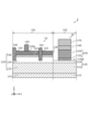
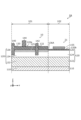
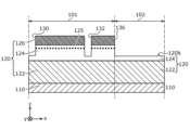
- FIG. 1A is a cross-sectional view of a nitride semiconductor device according to a first embodiment including a capacitor as a passive element.
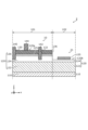
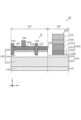
- FIG. 1B is a cross-sectional view showing a nitride semiconductor device according to the first embodiment including a resistor element as a passive element.
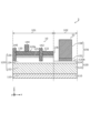
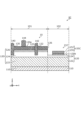
- FIG. 1C is a cross-sectional view showing a nitride semiconductor device according to the first embodiment including an inductor as an active element.
- FIG. 2A is a diagram showing a hexagonal close-packed crystal structure.
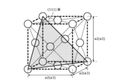
- FIG. 2B is a diagram showing a crystal structure of a face-centered cubic lattice structure.
- FIG. 1A is a cross-sectional view of a nitride semiconductor device according to a first embodiment including a capacitor as a passive element.
- FIG. 1B is a cross-sectional view showing a nitride semiconductor device according to the first embodiment including a resistor element as a passive element.
- FIG. 1C
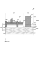
- FIG. 3A is a cross-sectional view of a nitride semiconductor device according to a first modification of the first embodiment, which includes a capacitor as a passive element.
- FIG. 3B is a cross-sectional view showing a nitride semiconductor device according to a first modification of the first embodiment, which includes a resistor element as a passive element.
- FIG. 3C is a cross-sectional view showing a nitride semiconductor device according to a first modification of the first embodiment, which includes an inductor as an active element.
- FIG. 4A is a cross-sectional view of a nitride semiconductor device according to a second modification of the first embodiment, which includes a capacitor as a passive element.
- FIG. 4B is a cross-sectional view showing a nitride semiconductor device according to Modification 2 of the first embodiment, which includes a resistor element as a passive element.
- FIG. 4C is a cross-sectional view showing a nitride semiconductor device according to Modification 2 of the first embodiment, which includes an inductor as an active element.
- FIG. 5A is a cross-sectional view of a nitride semiconductor device according to a third modification of the first embodiment, including a capacitor as a passive element.
- FIG. 5B is a cross-sectional view showing a nitride semiconductor device according to Modification 3 of the first embodiment, which includes a resistor element as a passive element.
- FIG. 5C is a cross-sectional view showing a nitride semiconductor device according to Modification 3 of the first embodiment, which includes an inductor as an active element.
- FIG. 6 is a flowchart showing a first example of a method for manufacturing a nitride semiconductor device according to the first embodiment.
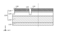
- FIG. 7A is a cross-sectional view illustrating a step included in a first example of a method for manufacturing a nitride semiconductor device according to the first embodiment.
- FIG. 7B is a cross-sectional view illustrating a step included in the first example of the method for manufacturing the nitride semiconductor device according to the first embodiment.
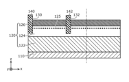
- FIG. 7C is a cross-sectional view illustrating a step included in the first example of the method for manufacturing the nitride semiconductor device according to the first embodiment.
- FIG. 7D is a cross-sectional view illustrating a step included in the first example of the method for manufacturing the nitride semiconductor device according to the first embodiment.
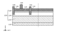
- FIG. 7E is a cross-sectional view illustrating a step included in the first example of the method for manufacturing the nitride semiconductor device according to the first embodiment.
- FIG. 7F is a cross-sectional view illustrating a step included in the first example of the method for manufacturing the nitride semiconductor device according to the first embodiment.
- FIG. 8 is a flowchart showing a second example of the method for manufacturing the nitride semiconductor device according to the first embodiment.
- FIG. 9A is a cross-sectional view illustrating a step included in the second example of the method for manufacturing the nitride semiconductor device according to the first embodiment.
- FIG. 9B is a cross-sectional view illustrating a step included in the second example of the method for manufacturing the nitride semiconductor device according to the first embodiment.
- FIG. 10 is a flowchart showing a third example of the method for manufacturing the nitride semiconductor device according to the first embodiment.
- FIG. 11 is a cross-sectional view of a nitride semiconductor device according to the second embodiment.
- FIG. 12 is a cross-sectional view of a nitride semiconductor device according to a modification of the second embodiment.
- a nitride semiconductor device is a nitride semiconductor device including an active element and a passive element, and includes a nitride semiconductor layer divided into an active region and an inactive region in a planar view, and a metal layer in contact with the nitride semiconductor layer in the inactive region, wherein the active element is provided in the active region, the passive element is provided in the inactive region, and the metal layer includes a coherent state or a metamorphic state with respect to the nitride semiconductor layer.
- the metal layer is provided in an inactive region, passive elements including the metal layer are less susceptible to carrier fluctuations during high-frequency operation. This makes it possible to realize a nitride semiconductor device with excellent high-frequency characteristics.
- the nitride semiconductor device is the nitride semiconductor device according to the first aspect, in which the nitride semiconductor layer includes a channel layer and a barrier layer provided above the channel layer, and the active element includes a two-dimensional electron gas generated near the interface between the channel layer and the barrier layer.
- a nitride semiconductor device is the nitride semiconductor device according to the second aspect, wherein, in the active region, the carrier density of the channel layer is 1 ⁇ 10 15 cm ⁇ 3 or more.
- a nitride semiconductor device is the nitride semiconductor device according to any one of the first to third aspects, wherein the nitride semiconductor layer has a stacked structure consisting of a plurality of layers, and in the inactive region, a carrier density of a top layer of the nitride semiconductor layer is less than 1 ⁇ 10 15 cm -3 .
- the nitride semiconductor device according to the fifth aspect of the present disclosure is a nitride semiconductor device according to any one of the first to fourth aspects, in which the contact surface between the nitride semiconductor layer and the metal layer in the inactive region is located below the top surface of the nitride semiconductor layer in the active region.
- the inactive region it is possible to prevent the generation of 2DEG by, for example, removing most or all of the barrier layer.
- the nitride semiconductor device is the nitride semiconductor device according to either the second or third aspect, in which the nitride semiconductor layer further includes a buffer layer provided below the channel layer, and the metal layer contacts the buffer layer in the inactive region.
- the buffer layer is generally a highly resistive layer with a sufficiently low carrier concentration. This reduces operational variation, thereby improving the high-frequency characteristics of passive elements.
- the nitride semiconductor device according to the seventh aspect of the present disclosure is a nitride semiconductor device according to any one of the first to sixth aspects, in which the nitride semiconductor layer includes an impurity region doped with C or Fe, and the metal layer contacts the impurity region in the inactive region.
- the impurity regions doped with C or Fe become highly resistive. This reduces operational variation, improving the high frequency characteristics of the passive element.
- the nitride semiconductor device is a nitride semiconductor device according to any one of the first to seventh aspects, in which the metal layer includes a barrier metal layer and a low-resistance metal layer provided above the barrier metal layer and having a lower resistance than the barrier metal layer.
- the passive elements are less susceptible to the effects of carrier fluctuations. This improves the high-frequency characteristics of the passive elements.
- the nitride semiconductor device according to the ninth aspect of the present disclosure is a nitride semiconductor device according to any one of the first to eighth aspects, in which the passive element is a resistive element including the metal layer.
- the nitride semiconductor device is a nitride semiconductor device according to any one of the first to eighth aspects, in which the passive element is a capacitor including the metal layer as a lower electrode.
- abnormal growth such as hillocks is suppressed, which makes it possible to suppress a decrease in the coverage of the insulating layer and electric field concentration. This makes it possible to suppress a decrease in the breakdown voltage of the capacitor.
- the nitride semiconductor device according to an eleventh aspect of the present disclosure is a nitride semiconductor device according to any one of the first to eighth aspects, in which the passive element is an inductor including the metal layer.
- the nitride semiconductor device is the nitride semiconductor device according to the eighth aspect, in which the lattice constant of the barrier metal layer is larger than the lattice constant of the low-resistance metal layer and is equal to or smaller than ⁇ 2 times the lattice constant of the a-axis of the nitride semiconductor layer at the contact surface with the metal layer.
- the nitride semiconductor device according to the thirteenth aspect of the present disclosure is the nitride semiconductor device according to the twelfth aspect, in which the lattice constant of each of the low-resistance metal layer and the barrier metal layer is 90% or more of ⁇ 2 times the lattice constant of the a-axis of the nitride semiconductor layer at the contact surface with the metal layer.
- the nitride semiconductor device according to the fourteenth aspect of the present disclosure is the nitride semiconductor device according to the eighth, twelfth or thirteenth aspect, in which the low-resistance metal layer has a face-centered cubic lattice structure composed of at least one element selected from the group consisting of Al, Cu, Au, Ag and Pt.
- the nitride semiconductor device according to the fifteenth aspect of the present disclosure is a nitride semiconductor device according to any one of the eighth aspect and the twelfth to fourteenth aspects, in which the barrier metal layer has a NaCl type structure composed of at least one element selected from the group consisting of Ti, Ta, W and Hf, and at least one element of N and C.
- the nitride semiconductor device is the nitride semiconductor device according to any one of the eighth aspect and the twelfth to fifteenth aspects, in which the metal layer is provided between the barrier metal layer and the nitride semiconductor layer and further includes a layer having a hexagonal close-packed structure composed of at least one element selected from the group consisting of Ti, Ta, W, and Hf.
- the nitride semiconductor device is a nitride semiconductor device according to any one of the first to sixteenth aspects, in which the active element includes a gate electrode, a source electrode, and a drain electrode, and at least one of the gate electrode, the source electrode, and the drain electrode includes the same material as at least a portion of the metal layer.
- the method for manufacturing a nitride semiconductor device is a method for manufacturing a nitride semiconductor device including an active element and a passive element, and includes the steps of forming a nitride semiconductor layer that is divided into an active region and an inactive region in a planar view, and forming a metal layer that contacts the nitride semiconductor layer in the inactive region, wherein the active element is provided in the active region, the passive element is provided in the inactive region, and the metal layer includes a coherent state or a metamorphic state with respect to the nitride semiconductor layer.
- the method for manufacturing a nitride semiconductor device is the method for manufacturing a nitride semiconductor device according to the 18th aspect, and includes the steps of forming a first recess in the nitride semiconductor layer, forming a source electrode and a drain electrode of the active element in the first recess, forming a gate electrode of the active element on the nitride semiconductor layer, and forming a second recess in the nitride semiconductor layer before forming the metal layer, and in the step of forming the metal layer, the metal layer is formed on the bottom surface of the second recess.
- the method for manufacturing a nitride semiconductor device according to the twentieth aspect of the present disclosure is the method for manufacturing a nitride semiconductor device according to the nineteenth aspect, in which the step of forming the first recess portion and the step of forming the second recess portion are performed simultaneously.
- the method for manufacturing a nitride semiconductor device according to the twenty-first aspect of the present disclosure is the method for manufacturing a nitride semiconductor device according to the nineteenth or twentieth aspect, in which the step of forming the metal layer and the step of forming the gate electrode are performed simultaneously.
- the method for manufacturing a nitride semiconductor device according to the twenty-second aspect of the present disclosure is the method for manufacturing a nitride semiconductor device according to the twenty-first aspect, in which the passive element is a capacitor including the metal layer as a lower electrode, and the method for manufacturing the nitride semiconductor device further includes a step of forming an insulating layer on the metal layer, and a step of forming an upper electrode on the insulating layer.
- abnormal growth such as hillocks is suppressed, which makes it possible to suppress a decrease in the coverage of the insulating layer and electric field concentration. This makes it possible to suppress a decrease in the breakdown voltage of the capacitor.
- each figure is a schematic diagram and is not necessarily an exact illustration. Therefore, for example, the scales of each figure do not necessarily match.
- substantially the same configuration is given the same reference numerals, and duplicate explanations are omitted or simplified.
- the x-axis, y-axis, and z-axis refer to the three axes of a three-dimensional Cartesian coordinate system.
- the z-axis direction is perpendicular to the main surface of the substrate, and the x-axis and y-axis directions are parallel to the main surface of the substrate.
- the "principal surface" of a substrate refers to the main surface of the substrate, for example the surface with the largest area, or the surface located opposite the surface with the largest area and having an area equivalent to that of the surface with the largest area.
- the principal surface is usually flat, but may include minute irregularities or curvatures.
- the terms “above” and “below” do not refer to the upward (vertically upward) and downward (vertically downward) directions in an absolute spatial sense, but are used as terms defined by a relative positional relationship based on the stacking order in the stacked configuration. Specifically, the positive direction of the z axis is considered to be “above”, and the negative direction of the z axis is considered to be “below”. Furthermore, the terms “above” and “below” are applied not only to cases where two components are arranged with a gap between them and another component exists between the two components, but also to cases where two components are arranged closely together and are in contact with each other.
- planar view means a view perpendicular to the main surface of the substrate. Specifically, “planar view” means a view from the positive or negative side of the z-axis.
- a layer consisting of one or more elements or compositions, and a layer composed of one or more elements or compositions mean that the layer contains substantially only one or more elements or compositions.
- the layer may contain other elements as impurities, for example elements that are unavoidable during manufacturing, at a rate of 1% or less.
- ordinal numbers such as “first” and “second” do not refer to the number or order of components, unless otherwise specified, but are used for the purpose of avoiding confusion between and distinguishing between components of the same type.
- the nitride semiconductor device includes an active element and a passive element.
- the active element is, for example, a transistor or a tunnel diode.
- the passive element is, for example, a capacitor, a resistive element, an inductor, etc.
- a nitride semiconductor device including a capacitor as a passive element will first be described with reference to FIG. 1A.
- a configuration including a resistive element or an inductor will be described later with reference to FIG. 1B or FIG. 1C.
- FIG. 1A is a cross-sectional view of a nitride semiconductor device 1 according to the present embodiment, which includes a capacitor 20 as a passive element. As shown in FIG. 1A, the nitride semiconductor device 1 includes a transistor 10 and a capacitor 20. The nitride semiconductor device 1 also includes a substrate 110 and a nitride semiconductor layer 120.
- the transistor 10 is an example of an active element and is provided in the active region 101.
- the capacitor 20 is an example of a passive element and is provided in the inactive region 102.
- the active region 101 and the inactive region 102 are regions that do not overlap with each other in a plan view.
- the active region 101 and the inactive region 102 are distinguished by the presence or absence of the second recess portion 136.
- the region in which the second recess portion 136 is provided is the inactive region 102, and the region in which the second recess portion 136 is not provided is the active region 101.
- the carrier concentration of the channel layer 124 is 1 ⁇ 10 15 cm ⁇ 3 or more.
- the carrier concentration of the channel layer 124 is lower than 1 ⁇ 10 15 cm ⁇ 3 .
- the transistor 10 includes a portion of each of the substrate 110 and the nitride semiconductor layer 120 located in the active region 101, a source electrode 140, a drain electrode 142, and a gate electrode 144.
- a 2DEG 125 is generated near the interface between the channel layer 124 and the barrier layer 126.
- the transistor 10 is a high electron mobility transistor (HEMT) that includes the 2DEG 125 as a channel.
- HEMT high electron mobility transistor
- the substrate 110 is a base substrate for forming the nitride semiconductor layer 120.
- the substrate 110 is, for example, a single crystal Si substrate whose main surface (upper surface) is a (111) surface.
- the resistivity of the substrate 110 is 1 k ⁇ cm or more, but is not limited to this.
- the resistivity of the substrate 110 may be 20 ⁇ cm or less.
- the substrate 110 is not limited to a single crystal Si substrate, and may be a substrate made of SiC, sapphire, GaN, AlN, or the like.
- the nitride semiconductor layer 120 is a layer made of a Group III nitride semiconductor.
- the nitride semiconductor layer 120 has a stacked structure made up of multiple layers. Specifically, as shown in FIG. 1A, the nitride semiconductor layer 120 includes a buffer layer 122, a channel layer 124, and a barrier layer 126.
- the nitride semiconductor layer 120 is divided into an active region 101 and an inactive region 102 in a plan view.
- the buffer layer 122 has the same configuration in the active region 101 and the inactive region 102.
- the portion of the channel layer 124 located in the active region 101 is thicker than the portion located in the inactive region 102.
- the barrier layer 126 is provided in the active region 101 and is not provided in the inactive region 102.
- the buffer layer 122 is provided above the substrate 110 and below the channel layer 124. Specifically, the buffer layer 122 is provided in contact with the upper surface of the substrate 110 and the lower surface of the channel layer 124.
- the buffer layer 122 is a layer made of a group III nitride semiconductor.
- the buffer layer 122 has a stacked structure of a plurality of layers each made of undoped Al x Ga 1-x N.
- x is 0 or more and 1 or less. That is, the buffer layer 122 may include an AlN layer or a GaN layer.
- the buffer layer 122 may include a layer that is doped with C or Fe to have a high resistance.
- the buffer layer 122 may also include a superlattice structure.
- the buffer layer 122 may have a single layer structure of a GaN layer, an AlGaN layer, or an AlN layer. Alternatively, the buffer layer 122 may not be provided.
- the channel layer 124 is provided above the substrate 110. Specifically, the channel layer 124 is provided in contact with the upper surface of the buffer layer 122.
- the channel layer 124 is a layer made of a group III nitride semiconductor.
- the channel layer 124 is a layer made of GaN, but may also contain In.
- the channel layer 124 has a different thickness between the active region 101 and the inactive region 102. Specifically, the thickness of the channel layer 124 in the active region 101 is thicker than the thickness of the channel layer 124 in the inactive region 102. The thickness of the channel layer 124 in the active region 101 is, for example, 150 nm. The thickness of the channel layer 124 in the inactive region 102 is, for example, half or less of the thickness of the channel layer 124 in the active region 101, but may be 10% or less, and is not limited thereto.
- the channel layer 124 in the inactive region 102 is formed to a thickness such that its upper surface (i.e., the bottom surface of the second recess portion 136, the contact surface 120b shown in FIG. 1A) is lower than the 2DEG 125 generated in the active region 101. The thickness of the channel layer 124 may be uniform between the active region 101 and the inactive region 102.
- the barrier layer 126 is provided above the channel layer 124.
- the barrier layer 126 is provided in contact with an upper surface of the channel layer 124.
- the barrier layer 126 is a layer made of a group III nitride semiconductor.
- the barrier layer 126 is a layer made of Al 0.25 Ga 0.75 N having a thickness of 13 nm, but is not limited thereto.
- the Al composition ratio of AlGaN constituting the barrier layer 126 may be a value selected from the range of 15% to 100%.
- the barrier layer 126 may also contain In.
- the band gap of the barrier layer 126 is larger than the band gap of the channel layer 124.
- 2DEG 125 is generated near the interface between the barrier layer 126 and the channel layer 124.
- the barrier layer 126 is not provided in the inactive region 102 but only in the active region 101, so that the 2DEG 125 is not generated in the inactive region 102 but only in the active region 101.
- the 2DEG 125 generated in the active region 101 functions as the channel of the transistor 10.
- the carrier density of the channel layer 124 is 1 ⁇ 10 15 cm ⁇ 3 or more at room temperature.
- the room temperature is, for example, 25° C.
- the nitride semiconductor layer 120 is provided with first recesses 130 and 132 and a second recess 136.
- the first recesses 130 and 132 and the second recess 136 are each a recess that penetrates the barrier layer 126 and in which at least a portion of the channel layer 124 has been removed.
- the first recess portion 130 is provided to reduce the contact resistance between the source electrode 140 and the 2DEG 125.
- the 2DEG 125 is exposed on the inner surface of the first recess portion 130, and the source electrode 140 comes into direct contact with the exposed 2DEG 125, thereby reducing the contact resistance.
- the first recess portion 132 is provided to reduce the contact resistance between the drain electrode 142 and the 2DEG 125.
- the 2DEG 125 is exposed on the inner surface of the first recess portion 132, and the drain electrode 142 comes into direct contact with the exposed 2DEG 125, thereby reducing the contact resistance.
- the position of the bottom surface of each of the first recesses 130 and 132 is located below the interface between the channel layer 124 and the barrier layer 126.
- the difference in the z-axis direction between the bottom surface of each of the first recesses 130 and 132 and the interface between the channel layer 124 and the barrier layer 126 is 10 nm or less.
- the second recess 136 is provided to inactivate the nitride semiconductor layer 120.
- the bottom surface (contact surface 120b) of the second recess 136 is located below the top surface 120a of the nitride semiconductor layer 120 in the active region 101.
- the barrier layer 126 is removed in the inactive region 102 by providing the second recess 136.
- the channel layer 124 is the top layer of the nitride semiconductor layer 120.
- the room temperature is, for example, 25° C.
- the source electrode 140 and the drain electrode 142 are provided at positions separated from each other in a plan view with the gate electrode 144 sandwiched therebetween.
- the source electrode 140 and the drain electrode 142 are each electrically connected to the 2DEG 125.
- the source electrode 140 is provided in the first recess portion 130 and is in contact with the 2DEG 125.
- the drain electrode 142 is provided in the first recess portion 132 and is in contact with the 2DEG 125.
- the source electrode 140 and the drain electrode 142 are both formed using a metal material that is ohmic-connected to the n-type nitride semiconductor.
- the source electrode 140 and the drain electrode 142 are multilayer electrode films having a laminated structure of a Ti film with a thickness of 30 nm and an Al film with a thickness of 200 nm provided on the Ti film.
- the thickness of the Ti film may be 2 nm or more and 40 nm or less, and the thickness of the Al film may be 100 nm or more and 200 nm or less.
- the source electrode 140 and the drain electrode 142 may be a single metal element selected from the group consisting of Ti, Ta, Hf, Zr, Ru, Al, Au, and W, or an alloy of a plurality of selected elements.
- the source electrode 140 and the drain electrode 142 may include a conductive metal nitride film such as TiN, WN, or TaN.
- the source electrode 140 and the drain electrode 142 are formed in the same process, but may also be formed in different processes using different materials.
- the gate electrode 144 is provided between the source electrode 140 and the drain electrode 142 in a plan view. In this embodiment, the gate electrode 144 is provided in contact with the top surface 120a of the nitride semiconductor layer 120.
- the gate electrode 144 is formed using a metal material that is Schottky-connected to the nitride semiconductor layer 120.
- the gate electrode 144 is a multi-layer electrode film having a laminated structure of a TiN film and an Al film provided on the TiN film.
- the TiN film and the Al film are the same as the barrier metal layer 152 and the low-resistance metal layer 154 of the capacitor 20, respectively.
- the gate electrode 144 may be formed using one selected from the group consisting of WN, TaN, HfN, Ni, Ti, Ta, W, Au, Pd, Pt, Hf, Ru, and Cu.
- An insulating layer or a p-type nitride semiconductor layer may be provided between the gate electrode 144 and the top surface 120a of the nitride semiconductor layer 120.
- the insulating layer has a single layer or a multilayer structure of, for example, SiN, SiO 2 , SiON, Al 2 O 3, or the like.
- the p-type nitride semiconductor layer is, for example, p-type GaN or AlGaN, or the like.
- the gate electrode 144 may be in ohmic contact with the p-type nitride semiconductor layer.
- the capacitor 20 includes a lower electrode 150, an insulating layer 160, and an upper electrode 170.
- the bottom electrode 150 is an example of a metal layer that contacts the nitride semiconductor layer 120 in the inactive region 102.
- the bottom electrode 150 includes a coherent state or a metamorphic state with respect to the nitride semiconductor layer 120. The coherent state and the metamorphic state will be described later.
- the bottom electrode 150 includes a barrier metal layer 152 and a low-resistance metal layer 154.
- the barrier metal layer 152 is provided to prevent the metal element (e.g., Cu) contained in the low-resistance metal layer 154 from diffusing into the nitride semiconductor layer 120.
- the barrier metal layer 152 is in contact with the nitride semiconductor layer 120 in the inactive region 102. Specifically, the barrier metal layer 152 is in contact with the contact surface 120b, which is the bottom surface of the second recess portion 136 and also part of the surface of the channel layer 124.
- the barrier metal layer 152 has a NaCl type structure composed of at least one element selected from the group consisting of Ti, Ta, W, and Hf, and at least one element of N and C.
- the barrier metal layer 152 is a single layer film composed of one compound selected from the group consisting of TiN, TaN, WN, HfN, TiC, and TaC, but may be a laminated film.
- the thickness of the barrier metal layer 152 is, for example, 5 nm to 200 nm, and is 20 nm as an example, but is not limited to this.
- the low-resistance metal layer 154 is provided above the barrier metal layer 152. Specifically, the low-resistance metal layer 154 is provided in contact with the upper surface of the barrier metal layer 152.
- the low-resistance metal layer 154 is a metal layer having a lower resistance than the barrier metal layer 152. By including the low-resistance metal layer 154 in the lower electrode 150, the parasitic resistance of the lower electrode 150 can be reduced.
- the low-resistance metal layer 154 has a face-centered cubic (fcc) structure composed of at least one element selected from the group consisting of Al, Cu, Au, Ag, and Pt.
- the low-resistance metal layer 154 is, for example, a single-layer film composed of one element selected from the group consisting of Al, Cu, Au, Ag, and Pt, but may also be a laminated film.
- the thickness of the low-resistance metal layer 154 is greater than the thickness of the barrier metal layer 152, and is, for example, 100 nm to 1000 nm, for example, 500 nm, but is not limited to this.
- the insulating layer 160 is provided between the lower electrode 150 and the upper electrode 170.
- the insulating layer 160 is formed using a film having a high dielectric constant and a high dielectric breakdown field.
- the insulating layer 160 is a single-layer film made of one compound selected from the group consisting of SiN, AlN, HfN, HfO , and Ta2O5 , but may be a laminated film.
- the thickness of the insulating layer 160 is not particularly limited and is determined based on the capacitance value, withstand voltage, etc. required for the capacitor 20.
- the upper electrode 170 is provided above the insulating layer 160.
- the upper electrode 170 is a single-layer film made of at least one element selected from the group consisting of Al, Cu, Au, Ag, and Pt, but may also be a laminated film.
- the lower electrode 150 is provided in the inactive region 102, so that it is less susceptible to carrier fluctuations during high-frequency operation. Therefore, it is possible to realize a capacitor 20 with excellent high-frequency characteristics.
- the lower electrode 150 of the capacitor 20 includes a coherent state or a metamorphic state with respect to the nitride semiconductor layer 120. As a result, the crystallinity of the lower electrode 150 is improved, and the high-frequency characteristics of the capacitor 20 are improved.
- the coherent state and the metamorphic state are described below.
- the coherent state is a state in which the layer retains the crystalline information of the underlying layer due to distortion of the lattice of the layer.
- the metamorphic state is a state in which the layer as a whole retains the crystalline information of the underlying layer due to the introduction of defects inside the layer. In other words, in both the coherent state and the metamorphic state, the layer (lower electrode 150 (barrier metal layer 152)) retains the crystalline information of the underlying layer (nitride semiconductor layer 120 (channel layer 124)).
- the barrier metal layer 152 and the low resistance metal layer 154 are in a coherent state or a metamorphic state with respect to the channel layer 124.
- the crystal structure and lattice constant must satisfy certain conditions.
- the crystal structure of the channel layer 124, which is the underlying layer, is a hexagonal close-packed (hcp) structure as shown in FIG. 2A.
- FIG. 2A is a diagram showing the crystal structure of a hexagonal close-packed (hcp) structure.
- FIG. 2B is a diagram showing the crystal structure of a face-centered cubic (fcc) structure.
- the crystal structure that is in a coherent state or metamorphic state with respect to the hcp structure is the fcc structure or the NaCl structure.
- the barrier metal layer 152 has a NaCl structure
- the low resistance metal layer 154 has the fcc structure shown in FIG. 2B.
- the NaCl structure can be considered to be substantially the same as the fcc structure shown in FIG. 2B.
- the (111) plane which is one of the crystal planes of the barrier metal layer 152, is parallel to and in the same direction as the (0002) plane, which is one of the crystal planes of the channel layer 124.
- the (111) plane which is one of the crystal planes of the low-resistance metal layer 154, is parallel to and in the same direction as the (0002) plane, which is one of the crystal planes of the channel layer 124.
- Both the barrier metal layer 152 and the low-resistance metal layer 154 are oriented only in the (111) plane.
- the barrier metal layer 152 and the low-resistance metal layer 154 are formed so that the six elements located at the vertices and midpoints of each side of the triangle (area shaded with dots) of the (111) plane shown in FIG. 2B correspond to the six elements shown in FIG. 2A.
- the six elements are represented by the (0001) plane instead of the (0002) plane.
- the lattice constants satisfy the following relationship.
- the lattice constant of the barrier metal layer 152 is larger than the lattice constant of the low-resistance metal layer 154 and is equal to or smaller than ⁇ 2 times the lattice constant of the a-axis of the nitride semiconductor layer 120 at the contact surface 120b with the lower electrode 150.
- the lattice constant of the a-axis of the channel layer 124 is "a1”
- the lattice constant of the barrier metal layer 152 is "a2”
- the lattice constant of the low-resistance metal layer 154 is "a3"
- the lattice constant a3 of the low-resistance metal layer 154 and the lattice constant a2 of the barrier metal layer 152 may be 90% or more of ⁇ 2 times the lattice constant a1 of the a-axis of the channel layer 124 at the contact surface 120b.
- the lattice constants of each layer may further satisfy the following inequalities (2) and (3).
- the difference between the lattice constant of the channel layer 124 multiplied by ⁇ 2 and the lattice constant of the barrier metal layer 152 or the low-resistance metal layer 154 is within ⁇ 10%.
- the crystallinity of each of the barrier metal layer 152 and the low-resistance metal layer 154 is further improved.
- the resistance of the low-resistance metal layer 154 is further reduced.
- the loss due to parasitic resistance components can be reduced.
- the reduction in coverage of the insulating layer 160 and the concentration of the electric field can be suppressed. Therefore, the reduction in the breakdown voltage of the capacitor 20 can be suppressed.
- the barrier metal layer 152 since the barrier metal layer 152 is provided, the formation of mixed crystals between the low-resistance metal layer 154 and the channel layer 124 is suppressed. This suppresses the generation of carriers in the channel layer 124, making the capacitor 20 less susceptible to the effects of carrier fluctuations during operation. This improves the high-frequency characteristics of the capacitor 20.
- Fig. 1B is a cross-sectional view of a nitride semiconductor device 2 including a resistor element 21 as a passive element.
- the nitride semiconductor device 2 includes a transistor 10 and a resistor element 21.
- the transistor 10 is the same as the transistor 10 included in the nitride semiconductor device 1 shown in Fig. 1A. The following description will focus on differences from the nitride semiconductor device 1, and descriptions of commonalities will be omitted or simplified.
- the resistive element 21 shown in FIG. 1B includes a metal layer 155.
- the metal layer 155 contacts the nitride semiconductor layer 120 in the inactive region 102.
- the metal layer 155 includes a coherent state or a metamorphic state with respect to the nitride semiconductor layer 120.
- the metal layer 155 can be formed using, for example, the same material as the barrier metal layer 152. Alternatively, the metal layer 155 may be formed using the same material as the low resistance metal layer 154. By adjusting the thickness, material, line width, and the like of the metal layer 155, a resistive element 21 having a desired resistance value can be formed.
- the crystallinity of the metal layer 155 is improved, similar to the lower electrode 150 of the nitride semiconductor device 1. This improves the resistance of the metal layer 155 to electromigration. This suppresses breaks or shorts in the resistance element 21, improving the high-frequency characteristics of the resistance element 21.
- Fig. 1C is a cross-sectional view of a nitride semiconductor device 3 including an inductor 22 as a passive element.
- the nitride semiconductor device 3 includes a transistor 10 and an inductor 22.
- the transistor 10 is the same as the transistor 10 included in the nitride semiconductor device 1 shown in Fig. 1A.
- the following description will focus on differences from the nitride semiconductor device 1, and descriptions of commonalities will be omitted or simplified.
- the inductor 22 shown in FIG. 1C includes a metal layer 156.
- the metal layer 156 contacts the nitride semiconductor layer 120 in the inactive region 102.
- the metal layer 156 includes a coherent state or a metamorphic state with respect to the nitride semiconductor layer 120.
- the metal layer 156 includes a barrier metal layer 152 and a low-resistance metal layer 158.
- the barrier metal layer 152 is the same as the barrier metal layer 152 provided in the nitride semiconductor device 1 shown in FIG. 1A.
- the low-resistance metal layer 158 is substantially the same as the low-resistance metal layer 154 provided in the nitride semiconductor device 1 shown in FIG. 1A, but has a different thickness. Specifically, the low-resistance metal layer 158 is thicker than the low-resistance metal layer 154. For example, the thickness and width of the low-resistance metal layer 158 are both 3 ⁇ m or more. This allows the metal layer 156 to have a lower resistance.
- the inductor 22 extends a certain length on the contact surface 120b of the inactive region 102.
- the inductor 22 may be formed in a straight line or in a coil shape in a plan view.
- the crystallinity of the metal layer 156 is improved, similar to the lower electrode 150 of the nitride semiconductor device 1. As a result, the crystallinity of the metal layer 156 is improved, and the parasitic resistance component of the inductor 22 can be reduced. This makes it possible to reduce losses due to the parasitic resistance component.
- ⁇ Modification 1> 3A is a cross-sectional view of a nitride semiconductor device 1A according to this modification including a capacitor 20 as a passive element. As shown in FIG. 3A, the nitride semiconductor device 1A differs from the nitride semiconductor device 1 in that a second recessed portion 136A is provided instead of the second recessed portion 136.
- the second recess 136A is provided to inactivate the nitride semiconductor layer 120.
- the bottom surface (contact surface 120b) of the second recess 136A is located below the top surface 120a of the nitride semiconductor layer 120 in the active region 101.
- the second recess 136A does not penetrate the barrier layer 126. That is, the barrier layer 126 remains even in the inactive region 102 and is the top layer of the nitride semiconductor layer 120.
- the contact surface 120b which is the bottom surface of the second recess 136A, is the surface of the barrier layer 126.
- the lower electrode 150 of the capacitor 20 is in contact with the barrier layer 126 in the inactive region 102 at a position lower than the top surface 120a of the active region 101 (a position closer to the substrate 110).
- the thickness of the barrier layer 126 in the inactive region 102 is smaller than the thickness of the barrier layer 126 in the active region 101.
- the thickness of the barrier layer 126 in the inactive region 102 piezoelectric polarization is suppressed, and 2DEG 125 is not generated.
- the carrier density of the channel layer 124 in the inactive region 102 becomes smaller than 1 ⁇ 10 15 cm ⁇ 3 at room temperature. Therefore, similar to the first embodiment, the high frequency characteristics of the nitride semiconductor device 1A can be improved.
- FIG. 3B is a cross-sectional view of a nitride semiconductor device 2A according to this modification that includes a resistive element 21 as a passive element.
- FIG. 3C is a cross-sectional view of a nitride semiconductor device 3A according to this modification that includes an inductor 22 as a passive element.
- the nitride semiconductor devices 2A and 3A are different from the nitride semiconductor devices 2 and 3, respectively, in that a second recessed portion 136A is provided instead of the second recessed portion 136.
- Both the metal layers 155 and 156 are in contact with the barrier layer 126 in the inactive region 102 at a position lower than the uppermost surface 120a of the active region 101 (a position closer to the substrate 110).
- the nitride semiconductor devices 2A and 3A that include these resistive elements 21 or inductors 22 can also improve the high-frequency characteristics in the same manner as in the first embodiment.
- ⁇ Modification 2> 4A is a cross-sectional view of a nitride semiconductor device 1B according to this modification including a capacitor 20 as a passive element. As shown in FIG. 4A, the nitride semiconductor device 1B differs from the nitride semiconductor device 1 in that a second recessed portion 136B is provided instead of the second recessed portion 136.
- the second recess 136B is provided to inactivate the nitride semiconductor layer 120.
- the bottom surface (contact surface 120b) of the second recess 136B is located below the top surface 120a of the nitride semiconductor layer 120 in the active region 101.
- the second recess 136B penetrates the barrier layer 126 and the channel layer 124 and reaches the buffer layer 122.
- the contact surface 120b which is the bottom surface of the second recess 136B, is the surface of the buffer layer 122.
- the barrier layer 126 and the channel layer 124 are not provided in the inactive region 102.
- the buffer layer 122 is the top layer of the nitride semiconductor layer 120.
- the lower electrode 150 is in contact with the buffer layer 122 in the inactive region 102 at a position lower than the top surface 120a of the active region 101 (a position closer to the substrate 110).
- the buffer layer 122 is an undoped nitride semiconductor layer, and has a carrier density of less than 1 ⁇ 10 15 cm ⁇ 3 at room temperature. Therefore, similar to the first embodiment, the high frequency characteristics of the nitride semiconductor device 1B can be improved.
- FIG. 4B is a cross-sectional view of a nitride semiconductor device 2B according to this modification that includes a resistive element 21 as a passive element.
- FIG. 4C is a cross-sectional view of a nitride semiconductor device 3B according to this modification that includes an inductor 22 as a passive element.
- the nitride semiconductor devices 2B and 3B are different from the nitride semiconductor devices 2 and 3, respectively, in that a second recessed portion 136B is provided instead of the second recessed portion 136.
- Both the metal layers 155 and 156 are in contact with the buffer layer 122 in the inactive region 102 at a position lower than the uppermost surface 120a of the active region 101 (a position closer to the substrate 110).
- the high-frequency characteristics can also be improved in the nitride semiconductor devices 2B and 3B that include these resistive elements 21 or inductors 22, as in the first embodiment.
- the buffer layer 122 may include an impurity region doped with C or Fe.
- the lower electrode 150 may be in contact with the impurity region.
- the impurity region doped with C or Fe has a high resistance. This suppresses operational variations, and improves the high frequency characteristics of the capacitor 20.
- the doping with C or Fe is performed during crystal growth. This makes it possible to maintain the crystal structure, unlike ion implantation.
- the contact surface 120b in the inactive region 102 may be at the same height as the interface between the channel layer 124 and the buffer layer 122 in the active region 101.
- Fig. 5A is a cross-sectional view of a nitride semiconductor device 1C according to this modification including a capacitor 20C as a passive element.
- the nitride semiconductor device 1C differs from the nitride semiconductor device 1 in that it includes a capacitor 20C instead of the capacitor 20.
- the capacitor 20C includes a lower electrode 150C instead of the lower electrode 150.
- the lower electrode 150C includes a metal underlayer 159 provided between the barrier metal layer 152 and the nitride semiconductor layer 120.
- the metal underlayer 159 has a hexagonal close-packed (hcp) structure composed of at least one element selected from the group consisting of Ti, Ta, W, and Hf.
- the thickness of the metal underlayer 159 is, for example, 2 nm to 50 nm, for example, 10 nm, but is not particularly limited.
- ⁇ 2 times the lattice constant of the a-axis of the metal underlayer 159 is equal to or greater than the lattice constant of the barrier metal layer 152, and is equal to or less than ⁇ 2 times the lattice constant of the a-axis of the nitride semiconductor layer 120 at the contact surface 120b with the lower electrode 150C.
- the lattice constant of the a-axis of the metal underlayer 159 is "a"
- the following inequality (4) is satisfied.
- the metal underlayer 159 By providing the metal underlayer 159, it is possible to improve the adhesion between the barrier metal layer 152 and the nitride semiconductor layer 120 (channel layer 124) while maintaining the crystallinity of the lower electrode 150C.
- FIG. 5B is a cross-sectional view of a nitride semiconductor device 2C according to this modified example that includes a resistive element 21C as a passive element.
- FIG. 5C is a cross-sectional view of a nitride semiconductor device 3C according to this modified example that includes an inductor 22C as a passive element.
- the resistive element 21C includes a metal layer 155C.
- the metal layer 155C includes a metal underlayer 159 provided between the barrier metal layer 152 and the channel layer 124.
- the barrier metal layer 152 is the same as the metal layer 155 provided in the nitride semiconductor device 2 according to the first embodiment.
- the inductor 22C includes a metal layer 156C.
- the metal layer 156C includes a metal underlayer 159 provided between the barrier metal layer 152 and the channel layer 124.
- nitride semiconductor devices 2C and 3C equipped with these resistive elements 21C or inductors 22C can improve the adhesion of metal layers 155C and 156C while maintaining the crystallinity of metal layers 155C and 156C.
- FIG. 6 is a flowchart showing a first example of a method for manufacturing a nitride semiconductor device 1 according to this embodiment.
- FIGS. 7A to 7F are cross-sectional views for explaining each step included in the first example of a method for manufacturing a nitride semiconductor device 1 according to this embodiment.
- a nitride semiconductor layer 120 is formed on a substrate 110 (S10). Specifically, a buffer layer 122, a channel layer 124, and a barrier layer 126 are formed in this order. Each layer is formed by growing the nitride semiconductor crystals through epitaxial growth using a method such as MOCVD (Metal-Organic Chemical Vapor Deposition). When forming the buffer layer 122, impurities such as C or Fe may be doped to increase resistance.
- MOCVD Metal-Organic Chemical Vapor Deposition
- a first recess portion 130 for the source electrode 140 and a first recess portion 132 for the drain electrode 142 are formed (S11).
- a resist pattern of a predetermined shape is formed by photolithography, and the barrier layer 126 and a part of the channel layer 124 within a predetermined range are removed by dry etching using the resist pattern, thereby forming the first recess portions 130 and 132.
- a source electrode 140 and a drain electrode 142 are formed in the first recessed portions 130 and 132, respectively (S12).
- a metal film is formed by EB (Electron Beam) deposition or sputtering, etc., so as to cover at least the first recessed portions 130 and 132, and the formed metal film is patterned by etching to form the source electrode 140 and the drain electrode 142.
- a gate electrode 144 is formed on the nitride semiconductor layer 120 (S13).
- a metal film is formed by EB deposition or sputtering so as to cover at least the region between the source electrode 140 and the drain electrode 142, and the formed metal film is patterned by etching to form the gate electrode 144.
- the process of forming the gate electrode 144 may be performed before the process of forming the source electrode 140 and the drain electrode 142.
- a second recess 136 for inactivation is formed (S14).
- a resist pattern of a predetermined shape is formed by photolithography, and the barrier layer 126 and a part of the channel layer 124 in the inactive region 102 are removed by dry etching or the like using the resist pattern, thereby forming the second recess 136.
- the 2DEG 125 in the channel layer 124 is no longer generated, and the carrier density at room temperature can be reduced to less than 1 ⁇ 10 15 cm ⁇ 3 .
- a metal layer (specifically, the lower electrode 150) is formed in contact with the nitride semiconductor layer 120 in the inactive region 102 (S15). Specifically, a barrier metal layer 152 and a low-resistance metal layer 154 are formed in this order on the contact surface 120b.
- a metal film is formed by EB deposition or sputtering, etc., so as to cover at least the contact surface 120b in the inactive region 102, and the formed metal film is patterned by etching to form the lower electrode 150.
- the lower electrode 150 is formed so as to be in a coherent state or a metamorphic state with respect to the nitride semiconductor layer 120 (channel layer 124).
- the growth rate of the electrode material is slowed down.
- the power supplied is reduced, and in the case of EB deposition, the temperature is lowered, or the distance between the target and the material is increased. This allows the growth rate of the electrode material to be slowed down, forming a lower electrode 150 that is in a coherent or metamorphic state with respect to the nitride semiconductor layer 120 (channel layer 124).
- an insulating layer 160 is formed on the metal layer (lower electrode 150), and an upper electrode 170 is formed on the formed insulating layer 160 (S16).
- the insulating layer 160 is formed, for example, by forming an insulating film so as to cover at least the lower electrode 150 by a plasma CVD (Chemical Vapor Depositino) method or the like, and then removing a part of the formed insulating film by etching.
- the upper electrode 170 is formed by forming a metal film so as to cover at least the insulating layer 160 by EB deposition or sputtering, and patterning the formed metal film by etching.
- a nitride semiconductor device 1 having a capacitor 20 as shown in FIG. 1A can be manufactured.
- a nitride semiconductor device 3 including an inductor 22 can be manufactured.
- a nitride semiconductor device 2 including a resistive element 21 can be manufactured.
- nitride semiconductor devices 1, 2, and 3 are merely examples, and the order of the steps, the content of the steps, etc. may be changed.
- the second recessed portion 136 (S14) only a portion of the barrier layer 126 in the inactive region 102 may be removed, leaving the barrier layer 126 of a predetermined thickness. This allows the nitride semiconductor device 1A, 2A or 3A according to Modification 1 to be formed.
- the channel layer 124 in the inactive region 102 may be completely removed.
- a portion of the buffer layer 122 in the inactive region 102 may be removed. This allows the nitride semiconductor device 1B, 2B or 3B according to Modification 2 to be formed.
- the second recess 136 may be formed simultaneously with the formation of an alignment mark for positioning.
- the alignment mark is usually formed between the step of forming the nitride semiconductor layer 120 (S10) and the step of forming the first recesses 130 and 132 (S11).
- a metal underlayer 159 may be formed before forming the barrier metal layer 152.
- the metal underlayer 159 is formed, for example, by forming a metal film by EB deposition or sputtering so as to cover at least the contact surface 120b in the inactive region 102, and then patterning the formed metal film by etching. This makes it possible to form the nitride semiconductor device 1C, 2C, or 3C according to the third modification.
- FIG. 8 is a flow chart showing a second example of the method for manufacturing the nitride semiconductor device 1 according to the present embodiment.
- FIGS. 9A and 9B are cross-sectional views for explaining each step included in the second example of the method for manufacturing the nitride semiconductor device 1 according to the present embodiment.
- the first recess 130 for the source electrode 140, the first recess 132 for the drain electrode 142, and the second recess 136 for inactivation are simultaneously formed (S21).
- a resist pattern of a predetermined shape is formed by photolithography, and the first recesses 130 and 132 and the second recess 136 are simultaneously formed by removing a part of the barrier layer 126 and the channel layer 124 from a predetermined range in the active region 101 and from the inactive region 102 by dry etching or the like using the resist pattern. Since they are formed simultaneously, the bottom surfaces of the first recesses 130 and 132 and the bottom surface (contact surface 120b) of the second recess 136 are located at the same height.
- a source electrode 140 and a drain electrode 142 are formed in the first recessed portions 130 and 132, respectively (S12).
- the subsequent processing is the same as that of the first example shown in FIG. 6, except that the process of forming the second recessed portion 136 (S14) is omitted, as shown in FIG. 8.
- the manufacturing process can be simplified, reducing the possibility of manufacturing errors and increasing the yield.
- FIG. 10 is a flowchart showing a third example of a method for manufacturing the nitride semiconductor device 1 according to this embodiment.
- the process from the formation of the nitride semiconductor layer 120 (S10) to the formation of the source electrode 140 and the drain electrode 142 (S12) is the same as the second example of the manufacturing method shown in FIG. 8.
- the gate electrode 144 and the metal layer (lower electrode 150) are formed at the same time (S33).
- the lower electrode 150 is formed at a slow growth rate to make it coherent or metamorphic with respect to the nitride semiconductor layer 120 (channel layer 124).
- the gate electrode 144 is also formed at the same rate.
- the configuration shown in FIG. 7F is obtained.
- the insulating layer 160 and the upper electrode 170 are formed in order, and the nitride semiconductor device 1 shown in FIG. 1A can be manufactured.
- the manufacturing process can be simplified, reducing the possibility of manufacturing errors and increasing yields.
- Embodiment 2 Next, a nitride semiconductor device according to embodiment 2 will be described.
- the main difference between embodiment 2 and embodiment 1 is that a passivation film that protects the surface of the nitride semiconductor layer is provided.
- the following description will focus on the differences from embodiment 1, and the description of commonalities will be omitted or simplified.
- FIG. 11 is a cross-sectional view of a nitride semiconductor device 201 according to the present embodiment.
- the nitride semiconductor device 201 differs from the nitride semiconductor device 1 according to the first embodiment in that it includes a capacitor 220 instead of the capacitor 20, and in that it includes passivation films 180 and 182.
- the passivation film 180 is provided to protect the surface of the nitride semiconductor layer 120. Specifically, the passivation film 180 covers the top surface 120a of the nitride semiconductor layer 120 in the active region 101.
- the passivation film 180 has openings for providing the source electrode 140, the drain electrode 142, and the gate electrode 144 in the active region 101. The openings for the source electrode 140 and the drain electrode 142 are provided at positions overlapping the first recesses 130 and 132 in a plan view.
- the top surface 120a of the nitride semiconductor layer 120 is exposed in the opening for the gate electrode 144, and the gate electrode 144 can be provided in contact with the top surface 120a. Note that an opening for the gate electrode 144 does not have to be provided, and the gate electrode 144 may be provided on the passivation film 180. In this case, the passivation film 180 can be used as a gate insulating film.
- the passivation film 182 is provided to protect the surface of the transistor 10. Specifically, the passivation film 182 covers the source electrode 140, the drain electrode 142, and the gate electrode 144, as well as the passivation film 180, in the active region 101. Furthermore, the passivation film 182 covers the inner surface of the second recess portion 136 in the inactive region 102.
- the passivation film 182 has an opening 183 for exposing the upper surface (contact surface 120b) of the nitride semiconductor layer 120 (channel layer 124) in the inactive region 102.
- the passivation films 180 and 182 are each formed using an insulating material.
- the passivation films 180 and 182 are each a single layer film or a multilayer film of SiN, SiO 2 , SiC, or the like, but are not limited thereto.
- the capacitor 220 includes a lower electrode 250, an insulating layer 260, and an upper electrode 270.
- the lower electrode 250 includes a barrier metal layer 252 and a low-resistance metal layer 254.
- the barrier metal layer 252, the low-resistance metal layer 254, the insulating layer 260, and the upper electrode 270 correspond to the barrier metal layer 152, the low-resistance metal layer 154, the insulating layer 160, and the upper electrode 170 in the first embodiment, respectively, and have different shapes and positions.
- the lower electrode 250 contacts the channel layer 124 exposed in the opening 183 provided in the passivation film 182.
- a portion of the lower electrode 250 (barrier metal layer 252) is provided on the upper surface of the passivation film 182.
- the length of the lower electrode 250 in the x-axis direction is longer than the length of the opening 183 in the x-axis direction.
- the portion of the lower electrode 250 that overlaps with the passivation film 182 in a planar view is neither in a coherent state nor in a metamorphic state.
- the lower electrode 250 of this embodiment includes a coherent state or a metamorphic state in the range that overlaps with the opening 183 of the passivation film 182 in a planar view.
- the upper electrode 270 is smaller than the opening 183 in a plan view. In a plan view, the entire upper electrode 270 is provided within the opening 183. That is, the upper electrode 270 is provided at a position where it overlaps with a portion of the lower electrode 250 that is in a coherent state or a metamorphic state in a plan view. In other words, the upper electrode 270 is provided at a position facing a portion of the lower electrode 250 that is highly crystalline and has a low resistance, and functions as a capacitor 220. Abnormal growth such as hillocks is suppressed at the portion of the lower electrode 250 that overlaps with the opening 183 in a plan view, so that a decrease in coverage of the insulating layer 260 and electric field concentration can be suppressed. This makes it possible to suppress a decrease in the breakdown voltage of the capacitor 220.
- the reliability can be improved by protecting the transistor 10 while suppressing the deterioration of the high frequency characteristics of the capacitor 220.
- a highly reliable nitride semiconductor device 201 with excellent high frequency characteristics can be realized.
- the passivation film 182 can also be used as the insulating layer 260 of the capacitor 220.
- Figure 12 is a cross-sectional view of a nitride semiconductor device 201A according to a modified example of this embodiment.
- the nitride semiconductor device 201A differs from the nitride semiconductor device 201 according to the second embodiment in that it includes a passivation film 282 and a capacitor 220A instead of the passivation film 182 and the capacitor 220, and that it includes an element isolation region 190. Also, in the inactive region 102, a second recess portion 236 is provided instead of the second recess portion 136.
- Capacitor 220A includes a lower electrode 251, a passivation film 282, and an upper electrode 270. A portion of the passivation film 282 is provided between the lower electrode 251 and the upper electrode 270.
- the lower electrode 251 corresponds to the lower electrode 250, and is different in that it is provided so as to fill the second recessed portion 236.
- the lower electrode 251 includes a laminated structure of a barrier metal layer and a low-resistance metal layer.
- the lower electrode 251 contacts the channel layer 124 at the contact surface 120b, which is the bottom surface of the second recessed portion 236.
- the lower electrode 251 includes a coherent state or a metamorphic state in the range where it overlaps with the bottom surface (contact surface 120b) of the second recessed portion 236 in a plan view.
- the lower electrode 251 also contacts the inner wall surface of the second recess portion 236. Specifically, the lower electrode 251 also contacts the barrier layer 126, and contacts the 2DEG 125 generated near the interface between the barrier layer 126 and the channel layer 124. For this reason, an element isolation region 190 is provided to cut off the electrical connection between the lower electrode 251 and the channel of the transistor 10.
- the element isolation region 190 is a region where impurities such as C or Fe are added to increase the resistance of the nitride semiconductor.
- the element isolation region 190 is provided at least in the channel layer 124 so as to block the 2DEG 125.
- the element isolation region 190 is provided by ion implantation so as to be continuous from the outermost surface of the barrier layer 126 to the channel layer 124 and the buffer layer 122.
- the inactive region 102 also includes the element isolation region 190.
- the inactive region 102 is considered to be the range that is separated by the element isolation region 190 from the 2DEG 125 of the active region 101 in which the transistor 10 is provided.
- the element isolation region 190 is formed by ion implantation, and therefore has a collapsed crystal structure. For this reason, even if a lower electrode 251 is formed on the element isolation region 190, the lower electrode 251 will not be in a coherent state or metamorphic state with respect to the nitride semiconductor layer 120.
- the second recess 236 is provided to expose a portion of the channel layer 124, and the lower electrode 251 is provided on the contact surface 120b, which is the exposed surface of the channel layer 124. This makes it possible to increase the crystallinity of the lower electrode 251, realize low resistance, and suppress abnormal growth such as hillocks.
- the passivation film 282 functions as an insulating layer for the capacitor 220A. This simplifies the manufacturing process compared to forming a dedicated insulating layer for the capacitor 220A. This reduces the possibility of manufacturing errors and increases the yield.
- the nitride semiconductor devices 201 and 201A are shown to have a capacitor as a passive element, but similar to the first embodiment, they may also have a resistive element or an inductor.
- the modified examples applied to the first embodiment can also be applied to the nitride semiconductor devices 201 and 201A.
- a plurality of passive elements may be provided in the inactive region 102.
- a plurality of at least one element selected from the group consisting of a capacitor 20, a resistive element 21, and an inductor 22 may be provided in the inactive region 102.
- the plurality of passive elements may be electrically connected to each other or may be electrically separated.
- a plurality of active elements may be provided in the active region 101.
- the first recesses 130 and 132 may not be provided, and the source electrode 140 and the drain electrode 142 may not be provided on the upper surface of the barrier layer 126. That is, the source electrode 140 and the drain electrode 142 may not be in contact with the channel layer 124 and the 2DEG 125.
- the nitride semiconductor layer 120 may not include the channel layer 124 and the barrier layer 126.
- the nitride semiconductor layer 120 may be a nitride semiconductor layer made of GaN, InGaN, or the like doped with n-type impurities such as Si.
- the transistor 10 does not have to be a HEMT, and may be another FET such as a MOSFET (Metal Oxide Semiconductor Field Effect Transistor).
- MOSFET Metal Oxide Semiconductor Field Effect Transistor
- a metal layer that is in a coherent state or a metamorphic state with respect to the nitride semiconductor layer 120 may be formed in the same process as the source electrode 140 or the drain electrode 142.
- the nitride semiconductor device according to the present disclosure can be used, for example, in a power amplifier for high output or high frequency applications, a wireless communication base station or terminal device in which the power amplifier is used, or a wireless power supply device that transmits power using microwaves.
- Nitride semiconductor device 10 Transistor 20, 20C, 220, 220A Capacitor 21, 21C Resistance element 22, 22C Inductor 101 Active region 102 Inactive region 110 Substrate 120 Nitride semiconductor layer 120a Top surface 120b Contact surface 122 Buffer layer 124 Channel layer 125 2DEG 126 Barrier layer 130, 132 First recessed portion 136, 136A, 136B, 236 Second recessed portion 140 Source electrode 142 Drain electrode 144 Gate electrode 150, 150C, 250, 251 Lower electrode 152, 252 Barrier metal layer 154, 158, 254 Low resistance metal layer 155, 155C, 156, 156C Metal layer 159 Metal underlayer 160, 260 Insulating layer 170, 270 Upper electrode 180, 182, 282 Passivation film 183 Opening 190 Element isolation region
Landscapes
- Junction Field-Effect Transistors (AREA)
Abstract
窒化物半導体装置(1)は、能動素子(10)と受動素子(20)とを備える窒化物半導体装置であって、平面視で活性領域(101)と不活性領域(102)とに区分される窒化物半導体層(120)と、不活性領域(102)で窒化物半導体層(120)に接する金属層(150)と、を備える。能動素子(10)は、活性領域(101)に設けられ、受動素子(20)は、不活性領域(102)に設けられる。金属層(150)は、窒化物半導体層(120)に対してコヒーレント状態またはメタモルフィック状態を含む。
Description
本開示は、窒化物半導体装置およびその製造方法に関する。
特許文献1には、GaN層と、GaN層上に設けられたAlGaN層と、AlGaN層上に設けられたp型GaN層と、p型GaN層上に設けられた金属層からなるインダクタと、を備える電子デバイスが開示されている。
金属層と接する半導体層がキャリアを含む場合、半導体層内には、金属層との界面から延びる空乏層が形成される。形成された空乏層は、寄生容量の増大の要因になる。寄生容量は、デバイスを高周波動作させた場合に配線遅延を引き起こすおそれがある。また、デバイスに対する電圧の印加状態に起因して、キャリア密度が変わると寄生容量の大きさも変化する。その結果、高周波動作の動作ばらつきが生じうる。このように、従来技術では、高周波特性が低下するおそれがある。
そこで、本開示は、高周波特性に優れた窒化物半導体装置およびその製造方法を提供する。
本開示の一態様に係る窒化物半導体装置は、能動素子と受動素子とを備える窒化物半導体装置であって、平面視で活性領域と不活性領域とに区分される窒化物半導体層と、前記不活性領域で前記窒化物半導体層に接する金属層と、を備え、前記能動素子は、前記活性領域に設けられ、前記受動素子は、前記不活性領域に設けられ、前記金属層は、前記窒化物半導体層に対してコヒーレント状態またはメタモルフィック状態を含む。
本開示の一態様に係る窒化物半導体装置の製造方法は、能動素子と受動素子とを備える窒化物半導体装置の製造方法であって、平面視で活性領域と不活性領域とに区分される窒化物半導体層を形成する工程と、前記不活性領域で前記窒化物半導体層に接する金属層を形成する工程と、を含み、前記能動素子は、前記活性領域に設けられ、前記受動素子は、前記不活性領域に設けられ、前記金属層は、前記窒化物半導体層に対してコヒーレント状態またはメタモルフィック状態を含む。
本開示によれば、高周波特性に優れた窒化物半導体装置およびその製造方法を提供することができる。
(本開示の概要)
本開示の第1態様に係る窒化物半導体装置は、能動素子と受動素子とを備える窒化物半導体装置であって、平面視で活性領域と不活性領域とに区分される窒化物半導体層と、前記不活性領域で前記窒化物半導体層に接する金属層と、を備え、前記能動素子は、前記活性領域に設けられ、前記受動素子は、前記不活性領域に設けられ、前記金属層は、前記窒化物半導体層に対してコヒーレント状態またはメタモルフィック状態を含む。
本開示の第1態様に係る窒化物半導体装置は、能動素子と受動素子とを備える窒化物半導体装置であって、平面視で活性領域と不活性領域とに区分される窒化物半導体層と、前記不活性領域で前記窒化物半導体層に接する金属層と、を備え、前記能動素子は、前記活性領域に設けられ、前記受動素子は、前記不活性領域に設けられ、前記金属層は、前記窒化物半導体層に対してコヒーレント状態またはメタモルフィック状態を含む。
これにより、金属層の結晶性が良くなるので、金属層の電気特性が良化(例えば、低抵抗化)して高周波特性を向上させることができる。また、金属層が不活性領域に設けられるので、金属層を含む受動素子は、高周波動作時のキャリアの変動の影響を受けにくくなる。よって、高周波特性に優れた窒化物半導体装置を実現することができる。
本開示の第2態様に係る窒化物半導体装置は、第1態様に係る窒化物半導体装置であって、前記窒化物半導体層は、チャネル層と、前記チャネル層の上方に設けられたバリア層と、を含み、前記能動素子は、前記チャネル層と前記バリア層との界面近傍に生じる二次元電子ガスを含む。
これにより、二次元電子ガス(2DEG)の高い電子移動度を利用することで、能動素子の高速動作が可能になる。例えば、スイッチング動作の高速化などが可能になり、窒化物半導体装置の高周波特性を向上させることができる。
本開示の第3態様に係る窒化物半導体装置は、第2態様に係る窒化物半導体装置であって、前記活性領域において、前記チャネル層のキャリア密度は、1×1015cm-3以上である。
これにより、2DEGの高い電子移動度を利用することで、能動素子の高速動作が可能になる。例えば、スイッチング動作の高速化などが可能になり、窒化物半導体装置の高周波特性を向上させることができる。
本開示の第4態様に係る窒化物半導体装置は、第1態様~第3態様のいずれか1つに係る窒化物半導体装置であって、前記窒化物半導体層は、複数の層からなる積層構造を有し、前記不活性領域において、前記窒化物半導体層の最上層のキャリア密度は、1×1015cm-3より小さい。
これにより、金属層と窒化物半導体層との寄生容量を低減することができるので、受動素子の高周波特性が向上する。
本開示の第5態様に係る窒化物半導体装置は、第1態様~第4態様のいずれか1つに係る窒化物半導体装置であって、前記不活性領域における前記窒化物半導体層と前記金属層との接触面は、前記活性領域における前記窒化物半導体層の最上面よりも下方に位置している。
これにより、不活性領域では、例えばバリア層の大部分または全部を除去することにより、2DEGを発生させないようにすることができる。このため、窒化物半導体層のキャリア濃度が低減されるので、金属層と窒化物半導体層との寄生容量を低減することができる。よって、受動素子の高周波特性を向上させることができる。
本開示の第6態様に係る窒化物半導体装置は、第2態様または第3態様のいずれか1つに係る窒化物半導体装置であって、前記窒化物半導体層は、前記チャネル層の下方に設けられたバッファ層をさらに含み、前記金属層は、前記不活性領域で前記バッファ層に接する。
これにより、バッファ層は一般的に高抵抗な層であり、キャリア濃度が十分に低い。このため、動作ばらつきが抑制されるので、受動素子の高周波特性を向上させることができる。
本開示の第7態様に係る窒化物半導体装置は、第1態様~第6態様のいずれか1つに係る窒化物半導体装置であって、前記窒化物半導体層は、CまたはFeがドープされた不純物領域を含み、前記金属層は、前記不活性領域で前記不純物領域に接する。
これにより、CまたはFeがドープされた不純物領域は高抵抗化する。このため、動作ばらつきが抑制されるので、受動素子の高周波特性を向上させることができる。
本開示の第8態様に係る窒化物半導体装置は、第1態様~第7態様のいずれか1つに係る窒化物半導体装置であって、前記金属層は、バリアメタル層と、前記バリアメタル層の上方に設けられ、前記バリアメタル層よりも抵抗が低い低抵抗金属層と、を含む。
これにより、低抵抗金属層と窒化物半導体層との混晶が抑制される。窒化物半導体層内でのキャリアの生成が抑制されるので、キャリアの変動の影響を受動素子が受けにくくなる。よって、受動素子の高周波特性を向上させることができる。
本開示の第9態様に係る窒化物半導体装置は、第1態様~第8態様のいずれか1つに係る窒化物半導体装置であって、前記受動素子は、前記金属層を含む抵抗素子である。
これにより、金属層の結晶性が良くなるので、エレクトロマイグレーションに対する耐性が高まる。抵抗素子の断線または短絡が抑制されるので、抵抗素子の高周波特性を向上させることができる。
本開示の第10態様に係る窒化物半導体装置は、第1態様~第8態様のいずれか1つに係る窒化物半導体装置であって、前記受動素子は、前記金属層を下部電極として含むキャパシタである。
これにより、下部電極である金属層の結晶性が良くなるので、下部電極の低抵抗化が実現され、寄生抵抗成分に起因するロスを低減することができる。また、ヒロックなどの異常成長が抑制されるため、絶縁層のカバレッジの低下および電界集中を抑制することができる。よって、キャパシタの耐圧の低下を抑制することができる。
本開示の第11態様に係る窒化物半導体装置は、第1態様~第8態様のいずれか1つに係る窒化物半導体装置であって、前記受動素子は、前記金属層を含むインダクタである。
これにより、金属層の結晶性が良くなるので、インダクタの寄生抵抗成分を低減することができる。よって、寄生抵抗成分に起因するロスを低減することができる。
本開示の第12態様に係る窒化物半導体装置は、第8態様に係る窒化物半導体装置であって、前記バリアメタル層の格子定数は、前記低抵抗金属層の格子定数より大きく、前記窒化物半導体層の、前記金属層との接触面におけるa軸の格子定数の√2倍以下である。
これにより、低抵抗金属層に生じうる転位を低減することができるので、低抵抗金属層のさらなる低抵抗化が可能になる。
本開示の第13態様に係る窒化物半導体装置は、第12態様に係る窒化物半導体装置であって、前記低抵抗金属層およびバリアメタル層の各々の格子定数は、前記窒化物半導体層の、前記金属層との接触面におけるa軸の格子定数の√2倍の90%以上である。
これにより、低抵抗金属層に生じうる転位を低減することができるので、低抵抗金属層のさらなる低抵抗化が可能になる。
本開示の第14態様に係る窒化物半導体装置は、第8態様、第12態様または第13態様に係る窒化物半導体装置であって、前記低抵抗金属層は、Al、Cu、Au、AgおよびPtからなる群から選択される少なくとも1種の元素によって構成される面心立方格子構造を有する。
これにより、金属層の結晶性を維持しながら低抵抗化が可能になる。
本開示の第15態様に係る窒化物半導体装置は、第8態様、第12態様~第14態様のいずれか1つに係る窒化物半導体装置であって、前記バリアメタル層は、Ti、Ta、WおよびHfからなる群から選択される少なくとも1種の元素と、NおよびCの少なくとも一方の元素とによって構成されるNaCl型構造を有する。
これにより、金属層の結晶性を維持しながら、金属層と窒化物半導体層との混晶を抑制することができる。
本開示の第16態様に係る窒化物半導体装置は、第8態様、第12態様~第15態様のいずれか1つに係る窒化物半導体装置であって、前記金属層は、前記バリアメタル層と前記窒化物半導体層との間に設けられ、Ti、Ta、WおよびHfからなる群から選択される少なくとも1種の元素によって構成される六方最密構造を有する層をさらに含む。
これにより、金属層の結晶性を維持しながら、金属層と窒化物半導体層との密着性を高めることができる。
本開示の第17態様に係る窒化物半導体装置は、第1態様~第16態様のいずれか1つに係る窒化物半導体装置であって、前記能動素子は、ゲート電極、ソース電極およびドレイン電極を含み、前記ゲート電極、前記ソース電極および前記ドレイン電極の少なくとも1つは、前記金属層の少なくとも一部と同じ材料を含む。
これにより、金属層と同じ材料を含む電極を、金属層と同一工程で形成することができる。
本開示の第18態様に係る窒化物半導体装置の製造方法は、能動素子と受動素子とを備える窒化物半導体装置の製造方法であって、平面視で活性領域と不活性領域とに区分される窒化物半導体層を形成する工程と、前記不活性領域で前記窒化物半導体層に接する金属層を形成する工程と、を含み、前記能動素子は、前記活性領域に設けられ、前記受動素子は、前記不活性領域に設けられ、前記金属層は、前記窒化物半導体層に対してコヒーレント状態またはメタモルフィック状態を含む。
これにより、結晶性の良好な金属層を形成することができ、金属層の電気特性が良化(例えば、低抵抗化)して高周波特性を向上させることができる。また、金属層が不活性領域に設けられるので、金属層を含む受動素子は、高周波動作時のキャリアの変動の影響を受けにくくなる。よって、高周波特性に優れた窒化物半導体装置を製造することができる。
本開示の第19態様に係る窒化物半導体装置の製造方法は、第18態様に係る窒化物半導体装置の製造方法であって、前記窒化物半導体層に第1リセス部を形成する工程と、前記第1リセス部内に前記能動素子のソース電極およびドレイン電極を形成する工程と、前記窒化物半導体層上に前記能動素子のゲート電極を形成する工程と、前記金属層を形成する前に前記窒化物半導体層に第2リセス部を形成する工程と、を含み、前記金属層を形成する工程では、前記第2リセス部の底面に前記金属層を形成する。
これにより、第2リセス部によって窒化物半導体層の不活化を容易に行うことができる。
本開示の第20態様に係る窒化物半導体装置の製造方法は、第19態様に係る窒化物半導体装置の製造方法であって、前記第1リセス部を形成する工程および前記第2リセス部を形成する工程は、同時に行われる。
これにより、第1リセス部および第2リセス部を同一工程で形成することができる。製造工程を簡略化することにより、製造誤差などが生じる可能性を低くすることができ、歩留まりを高めることができる。
本開示の第21態様に係る窒化物半導体装置の製造方法は、第19態様または第20態様に係る窒化物半導体装置の製造方法であって、前記金属層を形成する工程および前記ゲート電極を形成する工程は、同時に行われる。
これにより、金属層およびゲート電極を同一工程で形成することができる。製造工程を簡略化することにより、製造誤差などが生じる可能性を低くすることができ、歩留まりを高めることができる。
本開示の第22態様に係る窒化物半導体装置の製造方法は、第21態様に係る窒化物半導体装置の製造方法であって、前記受動素子は、前記金属層を下部電極として含むキャパシタであり、前記窒化物半導体装置の製造方法は、さらに、前記金属層上に絶縁層を形成する工程と、前記絶縁層上に上部電極を形成する工程と、を含む。
これにより、下部電極である金属層の結晶性が良くなるので、下部電極の低抵抗化が実現され、寄生抵抗成分に起因するロスを低減することができる。また、ヒロックなどの異常成長が抑制されるため、絶縁層のカバレッジの低下および電界集中を抑制することができる。よって、キャパシタの耐圧の低下を抑制することができる。
以下では、実施の形態について、図面を参照しながら具体的に説明する。
なお、以下で説明する実施の形態は、いずれも包括的または具体的な例を示すものである。以下の実施の形態で示される数値、形状、材料、構成要素、構成要素の配置位置および接続形態、製造工程、ならびに、製造工程の順序などは、一例であり、本開示を限定する主旨ではない。また、以下の実施の形態における構成要素のうち、独立請求項に記載されていない構成要素については、任意の構成要素として説明される。
また、各図は、模式図であり、必ずしも厳密に図示されたものではない。したがって、例えば、各図において縮尺などは必ずしも一致しない。また、各図において、実質的に同一の構成については同一の符号を付しており、重複する説明は省略または簡略化する。
また、本明細書において、平行または垂直などの要素間の関係性を示す用語、要素の形状を示す用語、および、数値範囲は、厳格な意味のみを表す表現ではなく、実質的に同等な範囲、例えば数%程度の差異をも含むことを意味する表現である。
また、本明細書および図面において、x軸、y軸およびz軸は、三次元直交座標系の三軸を示している。各実施の形態では、z軸方向を基板の主面に対して垂直な方向とし、基板の主面に平行な方向をx軸方向およびy軸方向としている。
なお、本明細書において、基板の「主面」とは、基板の主要な面であり、例えば、面積が最大となる面、または、当該面積が最大になる面の反対側に位置し、最大面積の面と同等の面積を有する面を意味する。主面は通常、平面であるが、微小な凹凸または湾曲が含まれていてもよい。半導体層、金属層または絶縁層などの各層の「主面」についても同様である。
また、本明細書において、「上方」および「下方」という用語は、絶対的な空間認識における上方向(鉛直上方)および下方向(鉛直下方)を指すものではなく、積層構成における積層順を基に相対的な位置関係により規定される用語として用いる。具体的には、z軸の正方向を「上方」とみなし、z軸の負方向を「下方」とみなしている。また、「上方」および「下方」という用語は、2つの構成要素が互いに間隔を空けて配置されて2つの構成要素の間に別の構成要素が存在する場合のみならず、2つの構成要素が互いに密着して配置されて2つの構成要素が接する場合にも適用される。
また、本明細書において、「平面視」とは、特に断りの無い限り、基板の主面に対して垂直な方向から見た場合を意味する。具体的には、「平面視」とは、z軸の正側または負側から見た場合を意味する。
また、1または複数の元素または組成物からなる層、および、1または複数の元素または組成物によって構成される層とは、当該層が実質的に1または複数の元素または組成物のみを含んでいることを意味する。ただし、当該層には、例えば製造上混入を避けられない元素など他の元素が不純物として、1%以下の割合で含まれていてもよい。
また、本明細書において、「第1」、「第2」などの序数詞は、特に断りの無い限り、構成要素の数または順序を意味するものではなく、同種の構成要素の混同を避け、区別する目的で用いられている。
(実施の形態1)
まず、実施の形態1に係る窒化物半導体装置について説明する。
まず、実施の形態1に係る窒化物半導体装置について説明する。
本実施の形態に係る窒化物半導体装置は、能動素子と、受動素子と、を備える。能動素子は、例えばトランジスタ、トンネルダイオードなどである。受動素子は、例えばキャパシタ、抵抗素子、インダクタなどである。以下ではまず、受動素子としてキャパシタを備える窒化物半導体装置について、図1Aを用いて説明する。抵抗素子またはインダクタを備える構成については、図1Bまたは図1Cを用いて後で説明する。
[キャパシタを備える窒化物半導体装置]
図1Aは、受動素子としてキャパシタ20を備える本実施の形態に係る窒化物半導体装置1の断面図である。図1Aに示すように、窒化物半導体装置1は、トランジスタ10と、キャパシタ20と、を備える。また、窒化物半導体装置1は、基板110と、窒化物半導体層120と、を備える。
図1Aは、受動素子としてキャパシタ20を備える本実施の形態に係る窒化物半導体装置1の断面図である。図1Aに示すように、窒化物半導体装置1は、トランジスタ10と、キャパシタ20と、を備える。また、窒化物半導体装置1は、基板110と、窒化物半導体層120と、を備える。
トランジスタ10は、能動素子の一例であり、活性領域101に設けられている。キャパシタ20は、受動素子の一例であり、不活性領域102に設けられている。
活性領域101および不活性領域102は、平面視で互いに重ならない領域である。本実施の形態では、第2リセス部136の有無によって活性領域101および不活性領域102が区分される。具体的には、第2リセス部136が設けられた領域が不活性領域102であり、第2リセス部136が設けられていない領域が活性領域101である。活性領域101では、チャネル層124のキャリア濃度が1×1015cm-3以上である。不活性領域102では、チャネル層124のキャリア濃度が1×1015cm-3より小さい。
トランジスタ10は、図1Aに示すように、基板110および窒化物半導体層120の各々のうちの活性領域101に位置する部分と、ソース電極140と、ドレイン電極142と、ゲート電極144と、を備える。窒化物半導体層120の活性領域101に位置する部分では、チャネル層124とバリア層126との界面近傍に2DEG125が生じる。トランジスタ10は、2DEG125をチャネルとして含む高電子移動度トランジスタ(High Electron Mobility Transistor:HEMT)である。
基板110は、窒化物半導体層120を形成するための下地基板である。基板110は、例えば、主面(上面)が(111)面であるSiの単結晶基板である。例えば、基板110の抵抗率は、1kΩcm以上であるが、これに限定されない。基板110の抵抗率は、20Ωcm以下であってもよい。また、基板110は、Siの単結晶基板に限らず、SiC、サファイア(Sapphire)、GaNまたはAlNなどからなる基板であってもよい。
窒化物半導体層120は、III族窒化物半導体からなる層である。窒化物半導体層120は、複数の層からなる積層構造を有する。具体的には、図1Aに示すように、窒化物半導体層120は、バッファ層122と、チャネル層124と、バリア層126と、を含む。
窒化物半導体層120は、平面視で活性領域101と不活性領域102とに区分される。本実施の形態では、バッファ層122は、活性領域101と不活性領域102とで同じ構成を有する。チャネル層124は、活性領域101に位置する部分の厚さが、不活性領域102に位置する部分の厚さよりも厚い。バリア層126は、活性領域101に設けられ、不活性領域102には設けられていない。
バッファ層122は、基板110の上方で、かつ、チャネル層124の下方に設けられている。具体的には、バッファ層122は、基板110の上面とチャネル層124の下面とにそれぞれ接触して設けられている。バッファ層122は、III族窒化物半導体からなる層である。例えば、バッファ層122は、各々がアンドープのAlxGa1-xNからなる複数の層の積層構造を有する。ここで、xは、0以上1以下である。すなわち、バッファ層122には、AlN層またはGaN層が含まれてもよい。バッファ層122は、CまたはFeがドープされることにより高抵抗化された層を含んでもよい。また、バッファ層122は、超格子構造を含んでもよい。なお、バッファ層122は、GaN層、AlGaN層またはAlN層の単層構造であってもよい。あるいは、バッファ層122は、設けられていなくてもよい。
チャネル層124は、基板110の上方に設けられている。具体的には、チャネル層124は、バッファ層122の上面に接触して設けられている。チャネル層124は、III族窒化物半導体からなる層である。例えば、チャネル層124は、GaNからなる層であるが、Inを含んでもよい。
本実施の形態では、チャネル層124は、活性領域101と不活性領域102とで厚さが異なっている。具体的には、活性領域101におけるチャネル層124の厚さは、不活性領域102におけるチャネル層124の厚さより厚い。活性領域101におけるチャネル層124の厚さは、例えば150nmである。不活性領域102におけるチャネル層124の厚さは、例えば、活性領域101におけるチャネル層124の厚さの半分以下であるが、10%以下であってもよく、これに限定されない。不活性領域102におけるチャネル層124は、その上面(すなわち、第2リセス部136の底面であり、図1Aに示す接触面120b)が、活性領域101に生じる2DEG125よりも下方になるような厚さで形成されている。なお、チャネル層124の厚さは、活性領域101と不活性領域102とで均一であってもよい。
バリア層126は、チャネル層124の上方に設けられている。例えば、バリア層126は、チャネル層124の上面に接触して設けられている。バリア層126は、III族窒化物半導体からなる層である。例えば、バリア層126は、厚さが13nmのAl0.25Ga0.75Nからなる層であるが、これに限らない。バリア層126を構成するAlGaNのAl組成比は、15%以上100%以下の範囲から選択された値であってもよい。また、バリア層126は、Inを含んでもよい。
バリア層126のバンドギャップは、チャネル層124のバンドギャップよりも大きい。バリア層126とチャネル層124との界面近傍には、2DEG125が生じる。本実施の形態では、バリア層126は、不活性領域102には設けられずに活性領域101のみに設けられているので、2DEG125も不活性領域102には生じずに、活性領域101のみに生じる。活性領域101に生じた2DEG125がトランジスタ10のチャネルとして機能する。活性領域101において、チャネル層124のキャリア密度は、常温で1×1015cm-3以上である。なお、常温は、例えば25℃である。
窒化物半導体層120には、第1リセス部130および132、ならびに、第2リセス部136が設けられている。第1リセス部130および132、ならびに、第2リセス部136はそれぞれ、バリア層126を貫通し、かつ、チャネル層124の少なくとも一部が除去された凹部である。
第1リセス部130は、ソース電極140と2DEG125とのコンタクト抵抗を低減するために設けられている。第1リセス部130の内面には、2DEG125が露出しており、露出した2DEG125にソース電極140が直接接触することにより、コンタクト抵抗を低減することができる。
第1リセス部132は、ドレイン電極142と2DEG125とのコンタクト抵抗を低減するために設けられている。第1リセス部132の内面には、2DEG125が露出しており、露出した2DEG125にドレイン電極142が直接接触することにより、コンタクト抵抗を低減することができる。
第1リセス部130および132の各々の底面の位置は、チャネル層124とバリア層126との界面よりも下方に位置している。第1リセス部130および132の各々の底面と、チャネル層124とバリア層126との界面とのz軸方向における差は、10nm以下である。
第2リセス部136は、窒化物半導体層120を不活化するために設けられている。第2リセス部136の底面(接触面120b)は、活性領域101における窒化物半導体層120の最上面120aよりも下方に位置している。具体的には、第2リセス部136が設けられることにより、不活性領域102ではバリア層126が除去される。不活性領域102では、チャネル層124が窒化物半導体層120の最上層である。その結果、チャネル層124内に2DEG125が発生しないようにでき、不活性領域102におけるチャネル層124のキャリア密度が常温で1×1015cm-3よりも小さくなる。なお、常温は、例えば25℃である。
ソース電極140およびドレイン電極142は、平面視において、間にゲート電極144を挟むように互いに離れた位置に設けられている。ソース電極140およびドレイン電極142はそれぞれ、2DEG125と電気的に接続されている。具体的には、ソース電極140は、第1リセス部130内に設けられて2DEG125に接触している。ドレイン電極142は、第1リセス部132内に設けられて2DEG125に接触している。
ソース電極140およびドレイン電極142はいずれも、n型の窒化物半導体に対してオーミック接続される金属材料を用いて形成されている。例えば、ソース電極140およびドレイン電極142は、厚さが30nmのTi膜と、当該Ti膜上に設けられた厚さが200nmのAl膜との積層構造を有する多層電極膜である。
なお、Ti膜の厚さは、2nm以上40nm以下であってもよく、Al膜の厚さは、100nm以上200nm以下であってもよい。また、ソース電極140およびドレイン電極142は、Ti、Ta、Hf、Zr、Ru、Al、AuおよびWからなる群から選択される1つの元素の金属単体、または、選択される複数の元素の合金であってもよい。また、ソース電極140およびドレイン電極142は、TiN、WN、TaNなどの導電性金属窒化膜を含んでもよい。ソース電極140およびドレイン電極142は、同一工程で形成されるが、異なる工程で異なる材料を用いて形成されてもよい。
ゲート電極144は、平面視において、ソース電極140およびドレイン電極142の間に設けられている。本実施の形態では、ゲート電極144は、窒化物半導体層120の最上面120aに接触して設けられている。
ゲート電極144は、窒化物半導体層120に対してショットキー接続される金属材料を用いて形成される。例えば、ゲート電極144は、TiN膜と、当該TiN膜上に設けられたAl膜との積層構造を有する多層電極膜である。TiN膜およびAl膜はそれぞれ、キャパシタ20のバリアメタル層152および低抵抗金属層154と同じである。ゲート電極144は、WN、TaN、HfN、Ni、Ti、Ta、W、Au、Pd、Pt、Hf、RuおよびCuからなる群から選択される1つを用いて形成されていてもよい。
なお、ゲート電極144と窒化物半導体層120の最上面120aとの間には、絶縁層またはp型の窒化物半導体層が設けられていてもよい。絶縁層は、例えば、SiN、SiO2、SiON、Al2O3などの単層または積層構造を有する。p型の窒化物半導体層は、例えば、p型のGaNまたはAlGaNなどである。p型の窒化物半導体層が設けられている場合、ゲート電極144は、p型の窒化物半導体層に対してオーミック接触されていてもよい。
続いて、キャパシタ20について説明する。図1Aに示すように、キャパシタ20は、下部電極150と、絶縁層160と、上部電極170と、を備える。
下部電極150は、不活性領域102で窒化物半導体層120に接する金属層の一例である。下部電極150は、窒化物半導体層120に対してコヒーレント状態またはメタモルフィック状態を含む。コヒーレント状態およびメタモルフィック状態については、後で説明する。本実施の形態では、下部電極150は、バリアメタル層152と、低抵抗金属層154と、を含む。
バリアメタル層152は、低抵抗金属層154に含まれる金属元素(例えば、Cu)が窒化物半導体層120に拡散するのを抑制するために設けられている。バリアメタル層152は、不活性領域102において、窒化物半導体層120に接触している。具体的には、バリアメタル層152は、第2リセス部136の底面であり、かつ、チャネル層124の表面の一部である接触面120bに接触している。
バリアメタル層152は、Ti、Ta、WおよびHfからなる群から選択される少なくとも1種の元素と、NおよびCの少なくとも一方の元素とによって構成されるNaCl型構造を有する。例えば、バリアメタル層152は、TiN、TaN、WN、HfN、TiCおよびTaCからなる群から選択される1つの化合物からなる単層膜であるが、積層膜であってもよい。バリアメタル層152の厚さは、例えば5nm以上200nm以下であり、一例として20nmであるが、これに限らない。
低抵抗金属層154は、バリアメタル層152の上方に設けられている。具体的には、低抵抗金属層154は、バリアメタル層152の上面に接触して設けられている。低抵抗金属層154は、バリアメタル層152よりも抵抗が低い金属層である。低抵抗金属層154を下部電極150が含むことにより、下部電極150の寄生抵抗を低減することができる。
低抵抗金属層154は、Al、Cu、Au、AgおよびPtからなる群から選択される少なくとも1種の元素によって構成される面心立方格子(face-centerd cubic:fcc)構造を有する。低抵抗金属層154は、例えば、Al、Cu、Au、AgおよびPtからなる群から選択される1つの元素からなる単層膜であるが、積層膜であってもよい。低抵抗金属層154の厚さは、バリアメタル層152の厚さよりも大きく、例えば100nm以上1000nm以下であり、一例として500nmであるが、これに限らない。
絶縁層160は、下部電極150と上部電極170との間に設けられている。絶縁層160は、高い誘電率および高い絶縁破壊電界を有する膜を用いて形成されている。例えば、絶縁層160は、SiN、AlN、HfN、HfOおよびTa2O5からなる群から選択される1つの化合物からなる単層膜であるが、積層膜であってもよい。絶縁層160の厚さは、特に限定されず、キャパシタ20に要求される容量値や耐圧などに基づいて決定された厚さである。
上部電極170は、絶縁層160の上方に設けられている。上部電極170は、Al、Cu、Au、AgおよびPtからなる群から選択される少なくとも1種の元素からなる単層膜であるが、積層膜であってもよい。
以上のように、本実施の形態に係る窒化物半導体装置1では、下部電極150が不活性領域102に設けられるので、高周波動作時のキャリアの変動の影響を受けにくい。よって、高周波特性に優れたキャパシタ20を実現することができる。
また、キャパシタ20が備える下部電極150は、窒化物半導体層120に対してコヒーレント状態またはメタモルフィック状態を含む。この結果、下部電極150の結晶性が高まり、キャパシタ20の高周波特性が向上する。以下では、コヒーレント状態およびメタモルフィック状態について説明する。
コヒーレント状態とは、層の格子が歪むことにより、層が下地の層の結晶情報を保持している状態である。メタモルフィック状態とは、層の内部に欠陥を導入することにより、層が全体として下地の層の結晶情報を保持している状態である。すなわち、コヒーレント状態およびメタモルフィック状態のいずれにおいても、層(下部電極150(バリアメタル層152))が下地の層(窒化物半導体層120(チャネル層124))の結晶情報を保持している状態になる。
バリアメタル層152および低抵抗金属層154がそれぞれ、チャネル層124に対して、コヒーレント状態またはメタモルフィック状態である。コヒーレント状態またはメタモルフィック状態にするためには、結晶構造と格子定数とが所定の条件を満たすことが求められる。
下地の層であるチャネル層124の結晶構造は、図2Aに示す六方最密(hexagonal close-packed:hcp)構造である。なお、図2Aは、六方最密(hcp)構造の結晶構造を示す図である。図2Bは、面心立方格子(fcc)構造の結晶構造を示す図である。
hcp構造に対してコヒーレント状態またはメタモルフィック状態になる結晶構造は、fcc構造またはNaCl構造である。本実施の形態では、バリアメタル層152がNaCl構造を有し、低抵抗金属層154が図2Bに示すfcc構造を有する。NaCl構造は、図2Bに示すfcc構造と実質的に同じとみなすことができる。
バリアメタル層152の結晶面の1つである(111)面は、チャネル層124の結晶面の1つである(0002)面に対して、平行かつ同一方位である。また、低抵抗金属層154の結晶面の1つである(111)面は、チャネル層124の結晶面の1つである(0002)面に対して、平行かつ同一方位である。バリアメタル層152および低抵抗金属層154はいずれも、(111)面のみに配向している。
具体的には、図2Bに示す(111)面の三角形(ドットの網掛けが付された領域)の頂点および各辺の中点に位置する6つの元素が、図2Aに示す6つの元素に対応するように、バリアメタル層152および低抵抗金属層154が形成される。なお、図2Aでは、(0002)面の代わりに(0001)面で6つの元素を表している。この場合において、格子定数が以下の関係を満たしている。
バリアメタル層152の格子定数は、低抵抗金属層154の格子定数より大きく、窒化物半導体層120の、下部電極150との接触面120bにおけるa軸の格子定数の√2倍以下である。すなわち、チャネル層124のa軸の格子定数を“a1”とし、バリアメタル層152の格子定数を“a2”とし、低抵抗金属層154の格子定数を“a3”とすると、以下の不等式(1)を満たす。
(1) a1×√2≧a2>a3
なお、“√2”は、2の平方根(1.4142・・・)を表している。
このように、窒化物半導体層120(チャネル層124)のa軸の格子定数の√2倍を基準として、バリアメタル層152、低抵抗金属層154の順に格子定数を小さくすることにより、低抵抗金属層154での転位の発生を抑制することができる。よって、下部電極150の低抵抗化が可能になる。
また、低抵抗金属層154の格子定数a3およびバリアメタル層152の格子定数a2は、チャネル層124の、接触面120bにおけるa軸の格子定数a1の√2倍の90%以上であってもよい。すなわち、各層の格子定数は、以下の不等式(2)および(3)をさらに満たしていてもよい。
(2) a3≧a1×√2×0.9
(3) a2≧a1×√2×0.9
(3) a2≧a1×√2×0.9
つまり、チャネル層124の格子定数の√2倍と、バリアメタル層152または低抵抗金属層154の格子定数との差分は、±10%以内である。このような関係を満たすことにより、バリアメタル層152および低抵抗金属層154の各々の結晶性がさらに高くなる。低抵抗金属層154に含まれる転位が低減することで、低抵抗金属層154のさらなる低抵抗化が実現される。また、下部電極150の低抵抗化によって、寄生抵抗成分に起因するロスを低減することができる。また、ヒロックなどの異常成長が抑制されるため、絶縁層160のカバレッジの低下および電界集中を抑制することができる。よって、キャパシタ20の耐圧の低下を抑制することができる。
また、本実施の形態では、バリアメタル層152が設けられているので、低抵抗金属層154とチャネル層124との混晶が抑制される。これにより、チャネル層124内でのキャリアの生成が抑制されるので、動作時のキャリアの変動の影響をキャパシタ20が受けにくくなる。よって、キャパシタ20の高周波特性を向上させることができる。
[抵抗素子を備える窒化物半導体装置]
次に、受動素子として抵抗素子を備える窒化物半導体装置について、図1Bを用いて説明する。図1Bは、受動素子として抵抗素子21を備える窒化物半導体装置2の断面図である。図1Bに示すように、窒化物半導体装置2は、トランジスタ10と、抵抗素子21と、を備える。トランジスタ10は、図1Aに示した窒化物半導体装置1が備えるトランジスタ10と同じである。以下では、窒化物半導体装置1との相違点を中心に説明を行い、共通点の説明を省略または簡略化する。
次に、受動素子として抵抗素子を備える窒化物半導体装置について、図1Bを用いて説明する。図1Bは、受動素子として抵抗素子21を備える窒化物半導体装置2の断面図である。図1Bに示すように、窒化物半導体装置2は、トランジスタ10と、抵抗素子21と、を備える。トランジスタ10は、図1Aに示した窒化物半導体装置1が備えるトランジスタ10と同じである。以下では、窒化物半導体装置1との相違点を中心に説明を行い、共通点の説明を省略または簡略化する。
図1Bに示す抵抗素子21は、金属層155を含む。金属層155は、不活性領域102で窒化物半導体層120に接している。金属層155は、窒化物半導体層120に対してコヒーレント状態またはメタモルフィック状態を含む。金属層155は、例えば、バリアメタル層152と同じ材料を用いて形成することができる。あるいは、金属層155は、低抵抗金属層154と同じ材料を用いて形成されてもよい。金属層155の厚さ、材料および線幅などを調整することにより、所望の抵抗値を有する抵抗素子21を形成することができる。
窒化物半導体装置2によれば、窒化物半導体装置1の下部電極150と同様に、金属層155の結晶性が良くなる。このため、金属層155のエレクトロマイグレーションに対する耐性が高まる。よって、抵抗素子21の断線または短絡が抑制されるので、抵抗素子21の高周波特性を向上させることができる。
[インダクタを備える窒化物半導体装置]
次に、受動素子としてインダクタを備える窒化物半導体装置について、図1Cを用いて説明する。図1Cは、受動素子としてインダクタ22を備える窒化物半導体装置3の断面図である。図1Cに示すように、窒化物半導体装置3は、トランジスタ10と、インダクタ22と、を備える。トランジスタ10は、図1Aに示した窒化物半導体装置1が備えるトランジスタ10と同じである。以下では、窒化物半導体装置1との相違点を中心に説明を行い、共通点の説明を省略または簡略化する。
次に、受動素子としてインダクタを備える窒化物半導体装置について、図1Cを用いて説明する。図1Cは、受動素子としてインダクタ22を備える窒化物半導体装置3の断面図である。図1Cに示すように、窒化物半導体装置3は、トランジスタ10と、インダクタ22と、を備える。トランジスタ10は、図1Aに示した窒化物半導体装置1が備えるトランジスタ10と同じである。以下では、窒化物半導体装置1との相違点を中心に説明を行い、共通点の説明を省略または簡略化する。
図1Cに示すインダクタ22は、金属層156を含む。金属層156は、不活性領域102で窒化物半導体層120に接している。金属層156は、窒化物半導体層120に対してコヒーレント状態またはメタモルフィック状態を含む。本実施の形態では、金属層156は、バリアメタル層152と、低抵抗金属層158と、を含む。
バリアメタル層152は、図1Aに示した窒化物半導体装置1が備えるバリアメタル層152と同じである。低抵抗金属層158は、図1Aに示した窒化物半導体装置1が備える低抵抗金属層154とほぼ同じであり、厚さが異なっている。具体的には、低抵抗金属層158は、低抵抗金属層154に比べて厚さが厚い。例えば、低抵抗金属層158の厚さおよび幅はいずれも3μm以上である。これにより、金属層156をより低抵抗化することができる。
インダクタ22は、不活性領域102の接触面120b上に一定の長さで延設されている。例えば、インダクタ22は、平面視で直線状に形成されていてもよく、コイル状に形成されていてもよい。
窒化物半導体装置3によれば、窒化物半導体装置1の下部電極150と同様に、金属層156の結晶性が良くなる。このため、金属層156の結晶性が良くなるので、インダクタ22の寄生抵抗成分を低減することができる。よって、寄生抵抗成分に起因するロスを低減することができる。
[変形例]
続いて、実施の形態1の複数の変形例について説明する。以下に示す変形例では、実施の形態1に係る窒化物半導体装置1、2および3との相違点を中心に説明を行い、共通点の説明を省略または簡略化する。
続いて、実施の形態1の複数の変形例について説明する。以下に示す変形例では、実施の形態1に係る窒化物半導体装置1、2および3との相違点を中心に説明を行い、共通点の説明を省略または簡略化する。
<変形例1>
図3Aは、受動素子としてキャパシタ20を備える本変形例に係る窒化物半導体装置1Aの断面図である。図3Aに示すように、窒化物半導体装置1Aでは、窒化物半導体装置1と比較して、第2リセス部136の代わりに第2リセス部136Aが設けられている点が相違する。
図3Aは、受動素子としてキャパシタ20を備える本変形例に係る窒化物半導体装置1Aの断面図である。図3Aに示すように、窒化物半導体装置1Aでは、窒化物半導体装置1と比較して、第2リセス部136の代わりに第2リセス部136Aが設けられている点が相違する。
第2リセス部136Aは、窒化物半導体層120を不活化するために設けられている。第2リセス部136Aの底面(接触面120b)は、活性領域101における窒化物半導体層120の最上面120aよりも下方に位置している。本変形例では、第2リセス部136Aは、バリア層126を貫通していない。すなわち、不活性領域102においても、バリア層126が残存しており、窒化物半導体層120の最上層である。第2リセス部136Aの底面である接触面120bは、バリア層126の表面である。キャパシタ20の下部電極150は、活性領域101の最上面120aよりも低い位置(基板110に近い位置)で、不活性領域102内においてバリア層126と接触している。
本変形例では、第2リセス部136Aが設けられることにより、バリア層126の不活性領域102における厚さは、バリア層126の活性領域101における厚さよりも小さい。不活性領域102におけるバリア層126の厚さが小さくなることで、ピエゾ分極が抑制されるので、2DEG125が発生しない。これにより、実施の形態1と同様に、不活性領域102におけるチャネル層124のキャリア密度が常温で1×1015cm-3よりも小さくなる。よって、実施の形態1と同様に、窒化物半導体装置1Aの高周波特性を高めることができる。
キャパシタ20の代わりに、抵抗素子21またはインダクタ22を備える場合も同様である。図3Bは、受動素子として抵抗素子21を備える本変形例に係る窒化物半導体装置2Aの断面図である。図3Cは、受動素子としてインダクタ22を備える本変形例に係る窒化物半導体装置3Aの断面図である。図3Bおよび図3Cに示すように、窒化物半導体装置2Aおよび3Aではそれぞれ、窒化物半導体装置2および3と比較して、第2リセス部136の代わりに第2リセス部136Aが設けられている点が相違する。金属層155および156はいずれも、活性領域101の最上面120aよりも低い位置(基板110に近い位置)で、不活性領域102内においてバリア層126に接触している。これらの抵抗素子21またはインダクタ22を備える窒化物半導体装置2Aおよび3Aについても、実施の形態1と同様に、高周波特性を高めることができる。
<変形例2>
図4Aは、受動素子としてキャパシタ20を備える本変形例に係る窒化物半導体装置1Bの断面図である。図4Aに示すように、窒化物半導体装置1Bでは、窒化物半導体装置1と比較して、第2リセス部136の代わりに第2リセス部136Bが設けられている点が相違する。
図4Aは、受動素子としてキャパシタ20を備える本変形例に係る窒化物半導体装置1Bの断面図である。図4Aに示すように、窒化物半導体装置1Bでは、窒化物半導体装置1と比較して、第2リセス部136の代わりに第2リセス部136Bが設けられている点が相違する。
第2リセス部136Bは、窒化物半導体層120を不活化するために設けられている。第2リセス部136Bの底面(接触面120b)は、活性領域101における窒化物半導体層120の最上面120aよりも下方に位置している。本変形例では、第2リセス部136Bは、バリア層126およびチャネル層124を貫通し、バッファ層122に達している。第2リセス部136Bの底面である接触面120bは、バッファ層122の表面である。不活性領域102には、バリア層126およびチャネル層124が設けられていない。不活性領域102では、バッファ層122が窒化物半導体層120の最上層である。下部電極150は、活性領域101の最上面120aよりも低い位置(基板110に近い位置)で、不活性領域102内においてバッファ層122と接触している。
バッファ層122は、アンドープの窒化物半導体層であり、キャリア密度は、常温で1×1015cm-3よりも小さくなる。よって、実施の形態1と同様に、窒化物半導体装置1Bの高周波特性を高めることができる。
キャパシタ20の代わりに、抵抗素子21またはインダクタ22を備える場合も同様である。図4Bは、受動素子として抵抗素子21を備える本変形例に係る窒化物半導体装置2Bの断面図である。図4Cは、受動素子としてインダクタ22を備える本変形例に係る窒化物半導体装置3Bの断面図である。図4Bおよび図4Cに示すように、窒化物半導体装置2Bおよび3Bではそれぞれ、窒化物半導体装置2および3と比較して、第2リセス部136の代わりに第2リセス部136Bが設けられている点が相違する。金属層155および156はいずれも、活性領域101の最上面120aよりも低い位置(基板110に近い位置)で、不活性領域102内においてバッファ層122に接触している。これらの抵抗素子21またはインダクタ22を備える窒化物半導体装置2Bおよび3Bについても、実施の形態1と同様に、高周波特性を高めることができる。
なお、バッファ層122には、CまたはFeがドープされた不純物領域が含まれてもよい。下部電極150は、当該不純物領域に接していてもよい。CまたはFeがドープされた不純物領域は高抵抗化する。このため、動作ばらつきが抑制されるので、キャパシタ20の高周波特性を向上させることができる。CまたはFeのドープは、結晶成長時に行われる。このため、イオン注入の場合とは異なり、結晶構造を維持することができる。
また、本変形例では、不活性領域102内において、バッファ層122の一部も除去されているが、バッファ層122は除去されていなくてもよい。すなわち、不活性領域102内の接触面120bは、活性領域101内におけるチャネル層124とバッファ層122との界面と同じ高さであってもよい。
<変形例3>
図5Aは、受動素子としてキャパシタ20Cを備える本変形例に係る窒化物半導体装置1Cの断面図である。図5Aに示すように、窒化物半導体装置1Cでは、窒化物半導体装置1と比較して、キャパシタ20の代わりにキャパシタ20Cを備える点が相違する。キャパシタ20Cは、キャパシタ20と比較して、下部電極150の代わりに下部電極150Cを含む。
図5Aは、受動素子としてキャパシタ20Cを備える本変形例に係る窒化物半導体装置1Cの断面図である。図5Aに示すように、窒化物半導体装置1Cでは、窒化物半導体装置1と比較して、キャパシタ20の代わりにキャパシタ20Cを備える点が相違する。キャパシタ20Cは、キャパシタ20と比較して、下部電極150の代わりに下部電極150Cを含む。
下部電極150Cは、バリアメタル層152と窒化物半導体層120との間に設けられた金属下地層159を含む。金属下地層159は、Ti、Ta、WおよびHfからなる群から選択される少なくとも1種の元素によって構成される六方最密(hcp)構造を有する。金属下地層159の厚さは、例えば2nm以上50nm以下であり、一例として10nmであるが、特に限定されない。
金属下地層159のa軸の格子定数の√2倍は、バリアメタル層152の格子定数以上であり、窒化物半導体層120の、下部電極150Cとの接触面120bにおけるa軸の格子定数の√2倍以下である。例えば、金属下地層159のa軸の格子定数を“a”とした場合、以下の不等式(4)を満たす。
(4) a1×√2≧a4×√2≧a2
金属下地層159が設けられることにより、下部電極150Cの結晶性を維持しながら、バリアメタル層152と窒化物半導体層120(チャネル層124)との密着性を高めることができる。
キャパシタ20の代わりに、抵抗素子またはインダクタを備える場合も同様である。図5Bは、受動素子として抵抗素子21Cを備える本変形例に係る窒化物半導体装置2Cの断面図である。図5Cは、受動素子としてインダクタ22Cを備える本変形例に係る窒化物半導体装置3Cの断面図である。
図5Bに示す窒化物半導体装置2Cでは、抵抗素子21Cが金属層155Cを含む。金属層155Cは、バリアメタル層152とチャネル層124との間に設けられた金属下地層159を含む。なお、バリアメタル層152は、実施の形態1に係る窒化物半導体装置2が備える金属層155と同じである。
図5Cに示す窒化物半導体装置3Cでは、インダクタ22Cが金属層156Cを含む。金属層156Cでは、バリアメタル層152とチャネル層124との間に設けられた金属下地層159を含む。
これらの抵抗素子21Cまたはインダクタ22Cを備える窒化物半導体装置2Cおよび3Cについても、窒化物半導体装置1Cと同様に、金属層155Cおよび156Cの結晶性を維持しながら、金属層155Cおよび156Cの密着性を高めることができる。
[製造方法]
続いて、実施の形態1に係る窒化物半導体装置1の製造方法について説明する。
続いて、実施の形態1に係る窒化物半導体装置1の製造方法について説明する。
図6は、本実施の形態に係る窒化物半導体装置1の製造方法の第1例を示すフローチャートである。図7A~図7Fは、本実施の形態に係る窒化物半導体装置1の製造方法の第1例に含まれる各工程を説明するための断面図である。
図6および図7Aに示すように、まず基板110上に窒化物半導体層120を形成する(S10)。具体的には、バッファ層122、チャネル層124およびバリア層126をこの順で形成する。各層の形成は、MOCVD(Metal-Organic Chemical Vapor Deposition)法などによるエピタキシャル成長によって、窒化物半導体を結晶成長させることによって行われる。バッファ層122の形成の際には、CまたはFeなどの高抵抗化するための不純物がドープされてもよい。
次に、図7Bに示すように、ソース電極140用の第1リセス部130およびドレイン電極142用の第1リセス部132を形成する(S11)。例えば、フォトリソグラフィによって所定形状のレジストパターンを形成し、当該レジストパターンを利用したドライエッチングなどによって、所定の範囲内のバリア層126とチャネル層124の一部とを除去することによって、第1リセス部130および132を形成する。
次に、図7Cに示すように、第1リセス部130および132内にそれぞれ、ソース電極140およびドレイン電極142を形成する(S12)。例えば、EB(Electron Beam)蒸着またはスパッタリングなどによって、少なくとも第1リセス部130および132を覆うように金属膜を形成し、形成した金属膜をエッチングでパターニングすることにより、ソース電極140およびドレイン電極142を形成する。
次に、図7Dに示すように、窒化物半導体層120上にゲート電極144を形成する(S13)。例えば、EB蒸着またはスパッタリングなどによって、少なくともソース電極140とドレイン電極142との間の領域を覆うように金属膜を形成し、形成した金属膜をエッチングでパターニングすることにより、ゲート電極144を形成する。なお、ゲート電極144の形成工程は、ソース電極140およびドレイン電極142の形成工程の前に行われてもよい。
次に、図7Eに示すように、不活化用の第2リセス部136を形成する(S14)。例えば、フォトリソグラフィによって所定形状のレジストパターンを形成し、当該レジストパターンを利用したドライエッチングなどによって、不活性領域102内のバリア層126とチャネル層124の一部とを除去することによって、第2リセス部136を形成する。不活性領域102では、バリア層126が除去されることによって、チャネル層124内の2DEG125が発生しなくなり、常温でのキャリア密度を1×1015cm-3より小さくすることができる。
次に、図7Fに示すように、不活性領域102で窒化物半導体層120に接する金属層(具体的には下部電極150)を形成する(S15)。具体的には、バリアメタル層152および低抵抗金属層154をこの順で接触面120b上に形成する。例えば、EB蒸着またはスパッタリングなどによって、少なくとも不活性領域102内の接触面120bを覆うように金属膜を形成し、形成した金属膜をエッチングでパターニングすることにより、下部電極150を形成する。このとき、窒化物半導体層120(チャネル層124)に対してコヒーレント状態またはメタモルフィック状態になるように下部電極150を形成する。具体的には、電極材料の成長速度を遅くする。例えば、スパッタリングの場合には供給するパワーを減らし、EB蒸着の場合、温度を低くし、あるいは、ターゲットと材料との距離を離す。これにより、電極材料の成長速度を遅くすることができ、窒化物半導体層120(チャネル層124)に対してコヒーレント状態またはメタモルフィック状態になる下部電極150を形成することができる。
次に、不活性領域102内において、金属層(下部電極150)上に絶縁層160を形成し、形成した絶縁層160上に上部電極170を形成する(S16)。絶縁層160は、例えば、プラズマCVD(Chemical Vapor Depositino)法などによって少なくとも下部電極150を覆うように絶縁膜を成膜した後、成膜した絶縁膜の一部をエッチングで除去することにより形成される。上部電極170は、EB蒸着またはスパッタリングなどによって、少なくとも絶縁層160を覆うように金属膜を形成し、形成した金属膜をエッチングでパターニングすることにより形成される。
以上の工程を経て、図1Aに示すキャパシタ20を備える窒化物半導体装置1を製造することができる。
なお、絶縁層160および上部電極170の形成工程(S16)を省略することで、インダクタ22を備える窒化物半導体装置3を製造することができる。また、絶縁層160および上部電極170の形成工程(S16)を省略し、さらに、金属層の形成工程(S15)では、低抵抗金属層154の形成を省略することにより、抵抗素子21を備える窒化物半導体装置2を製造することができる。
上述した窒化物半導体装置1、2および3の製造方法は、一例にすぎず、工程の順序の変更、工程の内容の変更などが行われてもよい。
例えば、第2リセス部136の形成工程(S14)では、不活性領域102内のバリア層126の一部のみを除去し、所定の厚さのバリア層126を残存させてもよい。これにより、変形例1に係る窒化物半導体装置1A、2Aまたは3Aを形成することができる。あるいは、第2リセス部136の形成工程では、不活性領域102内のチャネル層124を完全に除去してもよい。また、不活性領域102内のバッファ層122の一部を除去してもよい。これにより、変形例2に係る窒化物半導体装置1B、2Bまたは3Bを形成することができる。
また、第2リセス部136の形成は、位置合わせ用のアライメントマークの形成と同時に行われてもよい。アライメントマークの形成は、通常、窒化物半導体層120の形成工程(S10)と第1リセス部130および132の形成工程(S11)との間に行われる。
また、金属層(下部電極150)の形成工程(S15)では、バリアメタル層152を形成する前に、金属下地層159を形成してもよい。金属下地層159は、例えば、EB蒸着またはスパッタリングなどによって、少なくとも不活性領域102内の接触面120bを覆うように金属膜を形成し、形成した金属膜をエッチングでパターニングすることにより形成される。これにより、変形例3に係る窒化物半導体装置1C、2Cまたは3Cを形成することができる。
また、第1リセス部130および132を形成する工程(S11)と第2リセス部136を形成する工程(S14)とは、同時に行われてもよい。図8は、本実施の形態に係る窒化物半導体装置1の製造方法の第2例を示すフローチャートである。図9Aおよび図9Bはそれぞれ、本実施の形態に係る窒化物半導体装置1の製造方法の第2例に含まれる各工程を説明するための断面図である。
図8および図9Aに示すように、窒化物半導体層120を形成した後、ソース電極140用の第1リセス部130およびドレイン電極142用の第1リセス部132と、不活化用の第2リセス部136とを同時に形成する(S21)。例えば、フォトリソグラフィによって所定形状のレジストパターンを形成し、当該レジストパターンを利用したドライエッチングなどによって、活性領域101における所定の範囲内と不活性領域102内との各々のバリア層126とチャネル層124の一部とを除去することによって、第1リセス部130および132ならびに第2リセス部136を同時に形成する。同時に形成するので、第1リセス部130および132の各々の底面と、第2リセス部136の底面(接触面120b)とは、同じ高さに位置している。
その後、図9Bに示すように、第1リセス部130および132内にそれぞれ、ソース電極140およびドレイン電極142を形成する(S12)。以降の処理は、図8に示すように、第2リセス部136の形成工程(S14)が省略されている点を除いて、図6に示した第1例と同じである。
第1リセス部130および132、ならびに、第2リセス部136を同時に形成することで、製造工程を簡略化することにより、製造誤差などが生じる可能性を低くすることができ、歩留まりを高めることができる。
また、金属層(下部電極150)を形成する工程(S15)とゲート電極144を形成する工程(S13)とは、同時に行われてもよい。図10は、本実施の形態に係る窒化物半導体装置1の製造方法の第3例を示すフローチャートである。
図10に示すように、窒化物半導体層120の形成(S10)からソース電極140およびドレイン電極142の形成(S12)までの処理は、図8に示す製造方法の第2例と同じである。ソース電極140およびドレイン電極142を形成した後、ゲート電極144と金属層(下部電極150)とを同時に形成する(S33)。下部電極150は、窒化物半導体層120(チャネル層124)に対してコヒーレント状態またはメタモルフィック状態にするため、遅い成長速度で形成される。ゲート電極144の形成速度も同じになる。ゲート電極144と下部電極150とを同時に形成することで、図7Fに示す構成が得られる。以降、絶縁層160および上部電極170を順に形成することで、図1Aに示す窒化物半導体装置1を製造することができる。
ゲート電極144と金属層(下部電極150)とを同時に形成することで、製造工程を簡略化することにより、製造誤差などが生じる可能性を低くすることができ、歩留まりを高めることができる。
(実施の形態2)
続いて、実施の形態2に係る窒化物半導体装置について説明する。実施の形態2では、実施の形態1と比較して、窒化物半導体層の表面を保護するパッシベーション膜が設けられている点が主な相違点である。以下では、実施の形態1との相違点を中心に説明を行い、共通点の説明を省略または簡略化する。
続いて、実施の形態2に係る窒化物半導体装置について説明する。実施の形態2では、実施の形態1と比較して、窒化物半導体層の表面を保護するパッシベーション膜が設けられている点が主な相違点である。以下では、実施の形態1との相違点を中心に説明を行い、共通点の説明を省略または簡略化する。
図11は、本実施の形態に係る窒化物半導体装置201の断面図である。図11に示すように、窒化物半導体装置201は、実施の形態1に係る窒化物半導体装置1と比較して、キャパシタ20の代わりにキャパシタ220を備える点と、パッシベーション膜180および182を備える点とが相違する。
パッシベーション膜180は、窒化物半導体層120の表面を保護するために設けられている。具体的には、パッシベーション膜180は、活性領域101における窒化物半導体層120の最上面120aを覆っている。パッシベーション膜180には、活性領域101において、ソース電極140、ドレイン電極142およびゲート電極144の各々を設けるための開口が形成されている。ソース電極140およびドレイン電極142用の開口は、第1リセス部130および132と平面視で重なる位置に設けられている。また、ゲート電極144用の開口には、窒化物半導体層120の最上面120aが露出しており、ゲート電極144を最上面120a上に接触して設けることができる。なお、ゲート電極144用の開口は設けられていなくてもよく、パッシベーション膜180上にゲート電極144が設けられていてもよい。この場合、パッシベーション膜180をゲート絶縁膜として利用することができる。
パッシベーション膜182は、トランジスタ10の表面を保護するために設けられている。具体的には、パッシベーション膜182は、活性領域101内では、ソース電極140、ドレイン電極142およびゲート電極144、ならびに、パッシベーション膜180を覆っている。さらに、パッシベーション膜182は、不活性領域102内において第2リセス部136の内面を覆っている。パッシベーション膜182には、不活性領域102内において、窒化物半導体層120(チャネル層124)の上面(接触面120b)を露出させるための開口183が設けられている。
パッシベーション膜180および182はそれぞれ、絶縁性の材料を用いて形成されている。例えば、パッシベーション膜180および182はそれぞれ、SiN、SiO2、SiCなどの単層膜または積層膜であるが、これに限定されない。パッシベーション膜180および182が設けられていることで、電極間の絶縁性、および、電極と金属層(下部電極150)との間の絶縁性を高めることができ、リーク電流を抑制することができる。
本実施の形態では、キャパシタ220は、下部電極250と、絶縁層260と、上部電極270と、を含む。下部電極250は、バリアメタル層252と、低抵抗金属層254と、を含む。バリアメタル層252、低抵抗金属層254、絶縁層260および上部電極270はそれぞれ、実施の形態1に係るバリアメタル層152、低抵抗金属層154、絶縁層160および上部電極170に対応しており、各々の形状および配置位置が異なっている。
下部電極250は、パッシベーション膜182に設けられた開口183に露出したチャネル層124に接する。下部電極250(バリアメタル層252)の一部は、パッシベーション膜182の上面に設けられている。下部電極250のx軸方向の長さは、開口183のx軸方向の長さよりも長い。下部電極250のうち、平面視においてパッシベーション膜182に重なる部分は、コヒーレント状態およびメタモルフィック状態のいずれでもない。本実施の形態に係る下部電極250は、平面視において、パッシベーション膜182の開口183に重なる範囲において、コヒーレント状態またはメタモルフィック状態を含んでいる。
上部電極270は、平面視において、開口183よりも小さい。平面視において、上部電極270は全体が開口183内に設けられている。すなわち、上部電極270は、下部電極250のうち、コヒーレント状態またはメタモルフィック状態になっている部分と平面視で重なる位置に設けられている。つまり、下部電極250のうち結晶性が高く、低抵抗な部分と対向する位置に上部電極270が設けられており、キャパシタ220として機能する。下部電極250のうち、平面視で開口183に重なる位置ではヒロックなどの異常成長が抑制されるので、絶縁層260のカバレッジの低下および電界集中を抑制することができる。これにより、キャパシタ220の耐圧の低下を抑制することができる。
このように、本実施の形態に係る窒化物半導体装置201では、キャパシタ220の高周波特性の低下を抑制しながらトランジスタ10を保護することにより、信頼性を高めることができる。すなわち、本実施の形態によれば、高周波特性に優れた信頼性の高い窒化物半導体装置201を実現することができる。
なお、パッシベーション膜182をキャパシタ220の絶縁層260として利用することもできる。図12は、本実施の形態の変形例に係る窒化物半導体装置201Aの断面図である。
図12に示すように、窒化物半導体装置201Aは、実施の形態2に係る窒化物半導体装置201と比較して、パッシベーション膜182およびキャパシタ220の代わりにパッシベーション膜282およびキャパシタ220Aを備える点と、素子分離領域190が設けられている点とが相違する。また、不活性領域102には、第2リセス部136の代わりに、第2リセス部236が設けられている。
キャパシタ220Aは、下部電極251と、パッシベーション膜282と、上部電極270と、を含む。パッシベーション膜282の一部が下部電極251と上部電極270との間に設けられている。
下部電極251は、下部電極250に対応しており、第2リセス部236を埋めるように設けられている点が相違する。なお、図示していないが、下部電極251は、バリアメタル層と、低抵抗金属層との積層構造を含んでいる。下部電極251は、第2リセス部236の底面である接触面120bでチャネル層124と接している。これにより、下部電極251は、平面視において、第2リセス部236の底面(接触面120b)に重なる範囲において、コヒーレント状態またはメタモルフィック状態を含んでいる。
図12に示す例では、下部電極251は、第2リセス部236の内壁面にも接している。具体的には、下部電極251は、バリア層126にも接しており、バリア層126とチャネル層124との界面近傍に生じる2DEG125に接している。このため、下部電極251とトランジスタ10のチャネルとの電気的な接続を遮断するために、素子分離領域190が設けられている。
素子分離領域190は、例えばCまたはFeなどの窒化物半導体を高抵抗化するための不純物が添加された領域である。素子分離領域190は、2DEG125を遮断するように、少なくともチャネル層124に設けられている。例えば、イオン注入により、バリア層126の最表面から、チャネル層124およびバッファ層122にかけて連続するように素子分離領域190が設けられている。本変形例では、不活性領域102には、素子分離領域190も含まれる。言い換えると、トランジスタ10が設けられる活性領域101の2DEG125とは、素子分離領域190によって分離された範囲を不活性領域102とみなしている。
素子分離領域190は、イオン注入によって形成されるので、結晶構造が崩れている。このため仮に、素子分離領域190上に下部電極251を形成したとしても、下部電極251が窒化物半導体層120に対してコヒーレント状態またはメタモルフィック状態にはならない。本変形例では、第2リセス部236を設けることにより、チャネル層124の一部を露出させ、チャネル層124の露出した面である接触面120b上に下部電極251が設けられている。これにより、下部電極251の結晶性を高めることができ、低抵抗化を実現し、かつ、ヒロックなどの異常成長を抑制することができる。
また、本変形例では、パッシベーション膜282がキャパシタ220Aの絶縁層として機能している。キャパシタ220Aの専用の絶縁層を形成する場合に比べて、製造工程を簡略化することができる。よって、製造誤差などが生じる可能性を低くすることができ、歩留まりを高めることができる。
なお、実施の形態2および変形例では、窒化物半導体装置201および201Aが、受動素子としてキャパシタを備える例を示したが、実施の形態1と同様に、抵抗素子またはインダクタを備えてもよい。また、実施の形態1に適用される各変形例についても、窒化物半導体装置201および201Aにも適用することができる。
(他の実施の形態)
以上、1つまたは複数の態様に係る窒化物半導体装置について、実施の形態に基づいて説明したが、本開示は、これらの実施の形態に限定されるものではない。本開示の主旨を逸脱しない限り、当業者が思いつく各種変形を本実施の形態に施したもの、および、異なる実施の形態における構成要素を組み合わせて構築される形態も、本開示の範囲内に含まれる。
以上、1つまたは複数の態様に係る窒化物半導体装置について、実施の形態に基づいて説明したが、本開示は、これらの実施の形態に限定されるものではない。本開示の主旨を逸脱しない限り、当業者が思いつく各種変形を本実施の形態に施したもの、および、異なる実施の形態における構成要素を組み合わせて構築される形態も、本開示の範囲内に含まれる。
また、例えば、不活性領域102には、複数の受動素子が設けられてもよい。例えば、不活性領域102には、キャパシタ20、抵抗素子21およびインダクタ22からなる群から選択される少なくとも1つの素子が複数設けられていてもよい。複数の受動素子同士は、電気的に接続されていてもよく、電気的には分離していてもよい。同様に、活性領域101には、複数の能動素子が設けられていてもよい。
また、例えば、第1リセス部130および132は設けられていなくてもよく、ソース電極140およびドレイン電極142はそれぞれ、バリア層126の上面に設けられていなくてもよい。すなわち、ソース電極140およびドレイン電極142は、チャネル層124および2DEG125に接触していなくてもよい。
また、例えば、窒化物半導体層120は、チャネル層124およびバリア層126を含んでいなくてもよい。窒化物半導体層120は、Siなどのn型の不純物が添加されたGaN、InGaNなどからなる窒化物半導体層であってもよい。つまり、トランジスタ10は、HEMTでなくてもよく、MOSFET(Metal Oxide Semiconductor Field Effect Transistor)などの他のFETであってもよい。
また、例えば、窒化物半導体層120に対してコヒーレント状態またはメタモルフィック状態になる金属層は、ソース電極140またはドレイン電極142と同じ工程で形成されてもよい。
また、上記の各実施の形態は、請求の範囲またはその均等の範囲において種々の変更、置き換え、付加、省略などを行うことができる。
本開示に係る窒化物半導体装置は、例えば、高出力もしくは高周波用途の電力増幅器、当該電力増幅器が用いられる無線通信基地局もしくは端末機器、または、マイクロ波を利用した電力伝送を行うワイヤレス給電装置などに利用することができる。
1、1A、1B、1C、2、2A、2B、2C、3、3A、3B、3C、201、201A 窒化物半導体装置
10 トランジスタ
20、20C、220、220A キャパシタ
21、21C 抵抗素子
22、22C インダクタ
101 活性領域
102 不活性領域
110 基板
120 窒化物半導体層
120a 最上面
120b 接触面
122 バッファ層
124 チャネル層
125 2DEG
126 バリア層
130、132 第1リセス部
136、136A、136B、236 第2リセス部
140 ソース電極
142 ドレイン電極
144 ゲート電極
150、150C、250、251 下部電極
152、252 バリアメタル層
154、158、254 低抵抗金属層
155、155C、156、156C 金属層
159 金属下地層
160、260 絶縁層
170、270 上部電極
180、182、282 パッシベーション膜
183 開口
190 素子分離領域
10 トランジスタ
20、20C、220、220A キャパシタ
21、21C 抵抗素子
22、22C インダクタ
101 活性領域
102 不活性領域
110 基板
120 窒化物半導体層
120a 最上面
120b 接触面
122 バッファ層
124 チャネル層
125 2DEG
126 バリア層
130、132 第1リセス部
136、136A、136B、236 第2リセス部
140 ソース電極
142 ドレイン電極
144 ゲート電極
150、150C、250、251 下部電極
152、252 バリアメタル層
154、158、254 低抵抗金属層
155、155C、156、156C 金属層
159 金属下地層
160、260 絶縁層
170、270 上部電極
180、182、282 パッシベーション膜
183 開口
190 素子分離領域
Claims (22)
- 能動素子と受動素子とを備える窒化物半導体装置であって、
平面視で活性領域と不活性領域とに区分される窒化物半導体層と、
前記不活性領域で前記窒化物半導体層に接する金属層と、を備え、
前記能動素子は、前記活性領域に設けられ、
前記受動素子は、前記不活性領域に設けられ、
前記金属層は、前記窒化物半導体層に対してコヒーレント状態またはメタモルフィック状態を含む、
窒化物半導体装置。 - 前記窒化物半導体層は、チャネル層と、前記チャネル層の上方に設けられたバリア層と、を含み、
前記能動素子は、前記チャネル層と前記バリア層との界面近傍に生じる二次元電子ガスを含む、
請求項1に記載の窒化物半導体装置。 - 前記活性領域において、前記チャネル層のキャリア密度は、1×1015cm-3以上である、
請求項2に記載の窒化物半導体装置。 - 前記窒化物半導体層は、複数の層からなる積層構造を有し、
前記不活性領域において、前記窒化物半導体層の最上層のキャリア密度は、1×1015cm-3より小さい、
請求項1~3のいずれか1項に記載の窒化物半導体装置。 - 前記不活性領域における前記窒化物半導体層と前記金属層との接触面は、前記活性領域における前記窒化物半導体層の最上面よりも下方に位置している、
請求項1~4のいずれか1項に記載の窒化物半導体装置。 - 前記窒化物半導体層は、前記チャネル層の下方に設けられたバッファ層をさらに含み、
前記金属層は、前記不活性領域で前記バッファ層に接する、
請求項2または3に記載の窒化物半導体装置。 - 前記窒化物半導体層は、CまたはFeがドープされた不純物領域を含み、
前記金属層は、前記不活性領域で前記不純物領域に接する、
請求項1~6のいずれか1項に記載の窒化物半導体装置。 - 前記金属層は、
バリアメタル層と、
前記バリアメタル層の上方に設けられ、前記バリアメタル層よりも抵抗が低い低抵抗金属層と、を含む、
請求項1~7のいずれか1項に記載の窒化物半導体装置。 - 前記受動素子は、前記金属層を含む抵抗素子である、
請求項1~8のいずれか1項に記載の窒化物半導体装置。 - 前記受動素子は、前記金属層を下部電極として含むキャパシタである、
請求項1~8のいずれか1項に記載の窒化物半導体装置。 - 前記受動素子は、前記金属層を含むインダクタである、
請求項1~8のいずれか1項に記載の窒化物半導体装置。 - 前記バリアメタル層の格子定数は、前記低抵抗金属層の格子定数より大きく、前記窒化物半導体層の、前記金属層との接触面におけるa軸の格子定数の√2倍以下である、
請求項8に記載の窒化物半導体装置。 - 前記低抵抗金属層およびバリアメタル層の各々の格子定数は、前記窒化物半導体層の、前記金属層との接触面におけるa軸の格子定数の√2倍の90%以上である、
請求項12に記載の窒化物半導体装置。 - 前記低抵抗金属層は、Al、Cu、Au、AgおよびPtからなる群から選択される少なくとも1種の元素によって構成される面心立方格子構造を有する、
請求項8、12または13に記載の窒化物半導体装置。 - 前記バリアメタル層は、Ti、Ta、WおよびHfからなる群から選択される少なくとも1種の元素と、NおよびCの少なくとも一方の元素とによって構成されるNaCl型構造を有する、
請求項8、12~14のいずれか1項に記載の窒化物半導体装置。 - 前記金属層は、前記バリアメタル層と前記窒化物半導体層との間に設けられ、Ti、Ta、WおよびHfからなる群から選択される少なくとも1種の元素によって構成される六方最密構造を有する層をさらに含む、
請求項8、12~15のいずれか1項に記載の窒化物半導体装置。 - 前記能動素子は、ゲート電極、ソース電極およびドレイン電極を含み、
前記ゲート電極、前記ソース電極および前記ドレイン電極の少なくとも1つは、前記金属層の少なくとも一部と同じ材料を含む、
請求項1~16のいずれか1項に記載の窒化物半導体装置。 - 能動素子と受動素子とを備える窒化物半導体装置の製造方法であって、
平面視で活性領域と不活性領域とに区分される窒化物半導体層を形成する工程と、
前記不活性領域で前記窒化物半導体層に接する金属層を形成する工程と、を含み、
前記能動素子は、前記活性領域に設けられ、
前記受動素子は、前記不活性領域に設けられ、
前記金属層は、前記窒化物半導体層に対してコヒーレント状態またはメタモルフィック状態を含む、
窒化物半導体装置の製造方法。 - 前記窒化物半導体層に第1リセス部を形成する工程と、
前記第1リセス部内に前記能動素子のソース電極およびドレイン電極を形成する工程と、
前記窒化物半導体層上に前記能動素子のゲート電極を形成する工程と、
前記金属層を形成する前に前記窒化物半導体層に第2リセス部を形成する工程と、を含み、
前記金属層を形成する工程では、前記第2リセス部の底面に前記金属層を形成する、
請求項18に記載の窒化物半導体装置の製造方法。 - 前記第1リセス部を形成する工程および前記第2リセス部を形成する工程は、同時に行われる、
請求項19に記載の窒化物半導体装置の製造方法。 - 前記金属層を形成する工程および前記ゲート電極を形成する工程は、同時に行われる、
請求項19または20に記載の窒化物半導体装置の製造方法。 - 前記受動素子は、前記金属層を下部電極として含むキャパシタであり、
前記窒化物半導体装置の製造方法は、さらに、
前記金属層上に絶縁層を形成する工程と、
前記絶縁層上に上部電極を形成する工程と、を含む、
請求項21に記載の窒化物半導体装置の製造方法。
Priority Applications (3)
| Application Number | Priority Date | Filing Date | Title |
|---|---|---|---|
| CN202480041996.2A CN121420650A (zh) | 2023-07-06 | 2024-07-02 | 氮化物半导体装置及其制造方法 |
| JP2024566434A JP7618119B1 (ja) | 2023-07-06 | 2024-07-02 | 窒化物半導体装置およびその製造方法 |
| US19/423,481 US20260114028A1 (en) | 2023-07-06 | 2025-12-17 | Nitride semiconductor device and method for manufacturing the same |
Applications Claiming Priority (2)
| Application Number | Priority Date | Filing Date | Title |
|---|---|---|---|
| US202363525283P | 2023-07-06 | 2023-07-06 | |
| US63/525,283 | 2023-07-06 |
Related Child Applications (1)
| Application Number | Title | Priority Date | Filing Date |
|---|---|---|---|
| US19/423,481 Continuation US20260114028A1 (en) | 2023-07-06 | 2025-12-17 | Nitride semiconductor device and method for manufacturing the same |
Publications (1)
| Publication Number | Publication Date |
|---|---|
| WO2025009524A1 true WO2025009524A1 (ja) | 2025-01-09 |
Family
ID=94171550
Family Applications (1)
| Application Number | Title | Priority Date | Filing Date |
|---|---|---|---|
| PCT/JP2024/023920 Ceased WO2025009524A1 (ja) | 2023-07-06 | 2024-07-02 | 窒化物半導体装置およびその製造方法 |
Country Status (5)
| Country | Link |
|---|---|
| US (1) | US20260114028A1 (ja) |
| JP (1) | JP7618119B1 (ja) |
| CN (1) | CN121420650A (ja) |
| TW (1) | TW202525087A (ja) |
| WO (1) | WO2025009524A1 (ja) |
Citations (4)
| Publication number | Priority date | Publication date | Assignee | Title |
|---|---|---|---|---|
| JPH10303218A (ja) * | 1997-04-24 | 1998-11-13 | Fujitsu Ltd | 半導体装置及びその製造方法 |
| US20140091311A1 (en) * | 2012-09-28 | 2014-04-03 | Samsung Electronics Co., Ltd. | Nitride semiconductor based power converting device |
| WO2016017127A1 (ja) * | 2014-07-29 | 2016-02-04 | パナソニックIpマネジメント株式会社 | 窒化物半導体装置 |
| WO2022168800A1 (ja) * | 2021-02-03 | 2022-08-11 | 国立大学法人 東京大学 | 積層構造体及びその製造方法 |
-
2024
- 2024-07-02 CN CN202480041996.2A patent/CN121420650A/zh active Pending
- 2024-07-02 TW TW113124627A patent/TW202525087A/zh unknown
- 2024-07-02 JP JP2024566434A patent/JP7618119B1/ja active Active
- 2024-07-02 WO PCT/JP2024/023920 patent/WO2025009524A1/ja not_active Ceased
-
2025
- 2025-12-17 US US19/423,481 patent/US20260114028A1/en active Pending
Patent Citations (4)
| Publication number | Priority date | Publication date | Assignee | Title |
|---|---|---|---|---|
| JPH10303218A (ja) * | 1997-04-24 | 1998-11-13 | Fujitsu Ltd | 半導体装置及びその製造方法 |
| US20140091311A1 (en) * | 2012-09-28 | 2014-04-03 | Samsung Electronics Co., Ltd. | Nitride semiconductor based power converting device |
| WO2016017127A1 (ja) * | 2014-07-29 | 2016-02-04 | パナソニックIpマネジメント株式会社 | 窒化物半導体装置 |
| WO2022168800A1 (ja) * | 2021-02-03 | 2022-08-11 | 国立大学法人 東京大学 | 積層構造体及びその製造方法 |
Also Published As
| Publication number | Publication date |
|---|---|
| US20260114028A1 (en) | 2026-04-23 |
| CN121420650A (zh) | 2026-01-27 |
| TW202525087A (zh) | 2025-06-16 |
| JP7618119B1 (ja) | 2025-01-20 |
| JPWO2025009524A1 (ja) | 2025-01-09 |
Similar Documents
| Publication | Publication Date | Title |
|---|---|---|
| US11742418B2 (en) | Semiconductor device | |
| CN102651352B (zh) | 半导体装置、用于制造半导体装置的方法以及电子器件 | |
| TW201303967A (zh) | 化合物半導體裝置及其製造方法 | |
| TWI641133B (zh) | 半導體單元 | |
| US20210273086A1 (en) | Semiconductor device and fabricating method thereof | |
| CN117855265A (zh) | 高电子迁移率晶体管及其制作方法 | |
| TWI790655B (zh) | 半導體結構及高電子遷移率電晶體 | |
| TWI755277B (zh) | 高電子遷移率電晶體及其製作方法 | |
| JP5216184B2 (ja) | 化合物半導体装置およびその製造方法 | |
| TWI569439B (zh) | 半導體單元 | |
| WO2024048266A1 (ja) | 半導体デバイス、半導体モジュールおよび無線通信装置 | |
| US11967642B2 (en) | Semiconductor structure, high electron mobility transistor and fabrication method thereof | |
| JP7618119B1 (ja) | 窒化物半導体装置およびその製造方法 | |
| CN117616581A (zh) | 氮化物基半导体装置及其制造方法 | |
| JP5370441B2 (ja) | 窒化ガリウム系hemtの製造方法及び窒化ガリウム系hemt | |
| TW202301675A (zh) | 半導體結構及高電子遷移率電晶體 | |
| US20260020313A1 (en) | Semiconductor device | |
| CN114975573B (zh) | 高电子迁移率晶体管及其制作方法 | |
| CN112802802B (zh) | 基于su-8光阻胶的半导体功率器件及其制备方法和包括其的功率模块 | |
| CN115863401B (zh) | 常闭型晶体管及其制备方法 | |
| US11942519B2 (en) | Semiconductor structure and high electron mobility transistor | |
| US20240355869A1 (en) | Composite passive component and preparation method therefor | |
| TWI849920B (zh) | 高電子遷移率電晶體及其製造方法 | |
| TW202531888A (zh) | 半導體裝置及其形成方法 | |
| KR102059690B1 (ko) | Iii-v족 반도체 소자 및 그 제조 방법 |
Legal Events
| Date | Code | Title | Description |
|---|---|---|---|
| WWE | Wipo information: entry into national phase |
Ref document number: 2024566434 Country of ref document: JP |
|
| NENP | Non-entry into the national phase |
Ref country code: DE |