WO2025009376A1 - センサ素子および測距システム - Google Patents
センサ素子および測距システム Download PDFInfo
- Publication number
- WO2025009376A1 WO2025009376A1 PCT/JP2024/021970 JP2024021970W WO2025009376A1 WO 2025009376 A1 WO2025009376 A1 WO 2025009376A1 JP 2024021970 W JP2024021970 W JP 2024021970W WO 2025009376 A1 WO2025009376 A1 WO 2025009376A1
- Authority
- WO
- WIPO (PCT)
- Prior art keywords
- substrate
- region
- cmos
- sensor element
- transistor
- Prior art date
- Legal status (The legal status is an assumption and is not a legal conclusion. Google has not performed a legal analysis and makes no representation as to the accuracy of the status listed.)
- Ceased
Links
Images




Classifications
-
- H—ELECTRICITY
- H10—SEMICONDUCTOR DEVICES; ELECTRIC SOLID-STATE DEVICES NOT OTHERWISE PROVIDED FOR
- H10D—INORGANIC ELECTRIC SEMICONDUCTOR DEVICES
- H10D84/00—Integrated devices formed in or on semiconductor substrates that comprise only semiconducting layers, e.g. on Si wafers or on GaAs-on-Si wafers
- H10D84/80—Integrated devices formed in or on semiconductor substrates that comprise only semiconducting layers, e.g. on Si wafers or on GaAs-on-Si wafers characterised by the integration of at least one component covered by groups H10D12/00 or H10D30/00, e.g. integration of IGFETs
- H10D84/82—Integrated devices formed in or on semiconductor substrates that comprise only semiconducting layers, e.g. on Si wafers or on GaAs-on-Si wafers characterised by the integration of at least one component covered by groups H10D12/00 or H10D30/00, e.g. integration of IGFETs of only field-effect components
- H10D84/83—Integrated devices formed in or on semiconductor substrates that comprise only semiconducting layers, e.g. on Si wafers or on GaAs-on-Si wafers characterised by the integration of at least one component covered by groups H10D12/00 or H10D30/00, e.g. integration of IGFETs of only field-effect components of only insulated-gate FETs [IGFET]
-
- H—ELECTRICITY
- H10—SEMICONDUCTOR DEVICES; ELECTRIC SOLID-STATE DEVICES NOT OTHERWISE PROVIDED FOR
- H10D—INORGANIC ELECTRIC SEMICONDUCTOR DEVICES
- H10D84/00—Integrated devices formed in or on semiconductor substrates that comprise only semiconducting layers, e.g. on Si wafers or on GaAs-on-Si wafers
- H10D84/80—Integrated devices formed in or on semiconductor substrates that comprise only semiconducting layers, e.g. on Si wafers or on GaAs-on-Si wafers characterised by the integration of at least one component covered by groups H10D12/00 or H10D30/00, e.g. integration of IGFETs
- H10D84/82—Integrated devices formed in or on semiconductor substrates that comprise only semiconducting layers, e.g. on Si wafers or on GaAs-on-Si wafers characterised by the integration of at least one component covered by groups H10D12/00 or H10D30/00, e.g. integration of IGFETs of only field-effect components
- H10D84/83—Integrated devices formed in or on semiconductor substrates that comprise only semiconducting layers, e.g. on Si wafers or on GaAs-on-Si wafers characterised by the integration of at least one component covered by groups H10D12/00 or H10D30/00, e.g. integration of IGFETs of only field-effect components of only insulated-gate FETs [IGFET]
- H10D84/85—Complementary IGFETs, e.g. CMOS
-
- H—ELECTRICITY
- H10—SEMICONDUCTOR DEVICES; ELECTRIC SOLID-STATE DEVICES NOT OTHERWISE PROVIDED FOR
- H10D—INORGANIC ELECTRIC SEMICONDUCTOR DEVICES
- H10D89/00—Aspects of integrated devices not covered by groups H10D84/00 - H10D88/00
- H10D89/60—Integrated devices comprising arrangements for electrical or thermal protection, e.g. protection circuits against electrostatic discharge [ESD]
-
- H—ELECTRICITY
- H10—SEMICONDUCTOR DEVICES; ELECTRIC SOLID-STATE DEVICES NOT OTHERWISE PROVIDED FOR
- H10F—INORGANIC SEMICONDUCTOR DEVICES SENSITIVE TO INFRARED RADIATION, LIGHT, ELECTROMAGNETIC RADIATION OF SHORTER WAVELENGTH OR CORPUSCULAR RADIATION
- H10F30/00—Individual radiation-sensitive semiconductor devices in which radiation controls the flow of current through the devices, e.g. photodetectors
- H10F30/20—Individual radiation-sensitive semiconductor devices in which radiation controls the flow of current through the devices, e.g. photodetectors the devices having potential barriers, e.g. phototransistors
- H10F30/21—Individual radiation-sensitive semiconductor devices in which radiation controls the flow of current through the devices, e.g. photodetectors the devices having potential barriers, e.g. phototransistors the devices being sensitive to infrared, visible or ultraviolet radiation
- H10F30/22—Individual radiation-sensitive semiconductor devices in which radiation controls the flow of current through the devices, e.g. photodetectors the devices having potential barriers, e.g. phototransistors the devices being sensitive to infrared, visible or ultraviolet radiation the devices having only one potential barrier, e.g. photodiodes
- H10F30/225—Individual radiation-sensitive semiconductor devices in which radiation controls the flow of current through the devices, e.g. photodetectors the devices having potential barriers, e.g. phototransistors the devices being sensitive to infrared, visible or ultraviolet radiation the devices having only one potential barrier, e.g. photodiodes the potential barrier working in avalanche mode, e.g. avalanche photodiodes
-
- H—ELECTRICITY
- H10—SEMICONDUCTOR DEVICES; ELECTRIC SOLID-STATE DEVICES NOT OTHERWISE PROVIDED FOR
- H10F—INORGANIC SEMICONDUCTOR DEVICES SENSITIVE TO INFRARED RADIATION, LIGHT, ELECTROMAGNETIC RADIATION OF SHORTER WAVELENGTH OR CORPUSCULAR RADIATION
- H10F39/00—Integrated devices, or assemblies of multiple devices, comprising at least one element covered by group H10F30/00, e.g. radiation detectors comprising photodiode arrays
- H10F39/10—Integrated devices
- H10F39/12—Image sensors
- H10F39/18—Complementary metal-oxide-semiconductor [CMOS] image sensors; Photodiode array image sensors
Definitions
- This disclosure relates to a sensor element and a ranging system, and in particular to a sensor element and a ranging system that enable greater functionality while maintaining pixel size.
- Distance image sensors that measure distance using the ToF (Time-of-Flight) method are known.
- Distance image sensors use, for example, a pixel array in which pixels using SPADs (Single Photon Avalanche Diodes) are arranged in a matrix.
- SPADs Single Photon Avalanche Diodes
- avalanche amplification occurs when a single photon enters a high-electric field PN junction region while a voltage greater than the breakdown voltage is applied. By detecting the timing at which the current flows at this time, it is possible to measure distance with high precision.
- Patent Document 1 proposes that in order to reduce the size and improve the functionality of a sensor element with a stacked structure, some of the multiple transistors that output a signal according to the cathode voltage or anode voltage of the SPAD are provided in a well formed in the semiconductor substrate of the sensor board.
- This disclosure was made in light of these circumstances, and aims to make it possible to achieve even greater functionality while maintaining pixel size.
- the sensor element disclosed herein is a sensor element comprising a sensor substrate on which a single photon avalanche diode (SPAD) is provided for each pixel, a complementary metal oxide semiconductor (CMOS) substrate laminated on the sensor substrate and provided with transistors for signal readout, a logic substrate laminated on the CMOS substrate and provided with a logic circuit, and a through electrode that penetrates the CMOS substrate and electrically connects the anode region of the sensor substrate to the CMOS substrate.
- CMOS complementary metal oxide semiconductor
- the distance measurement system disclosed herein includes an illumination device that emits irradiation light, and a sensor element that detects reflected light from the irradiation light.
- the sensor element is a distance measurement system having a sensor substrate on which a single photon avalanche diode (SPAD) is provided for each pixel, a complementary metal oxide semiconductor (CMOS) substrate that is laminated on the sensor substrate and has transistors for signal readout, a logic substrate that is laminated on the CMOS substrate and has a logic circuit, and a through electrode that penetrates the CMOS substrate and electrically connects the anode region of the sensor substrate to the CMOS substrate.
- CMOS complementary metal oxide semiconductor
- a sensor substrate on which a SPAD is provided for each pixel a CMOS substrate laminated on the sensor substrate and provided with transistors for signal readout, a logic substrate laminated on the CMOS substrate and provided with a logic circuit, and a through electrode that penetrates the CMOS substrate and electrically connects the anode region of the sensor substrate to the CMOS substrate are provided.
- FIG. 1 is a cross-sectional view showing a configuration example of a sensor element to which the technology according to the present disclosure is applied.
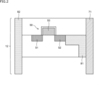
- FIG. 2 is a cross-sectional view showing a configuration example of a CMOS substrate.
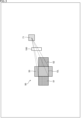
- FIG. 2 is a plan view showing a configuration example of a CMOS substrate.
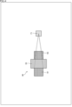
- FIG. 2 is a plan view showing a configuration example of a CMOS substrate according to the first embodiment;
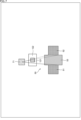
- FIG. 4 is a plan view showing another configuration example of the CMOS substrate according to the first embodiment.
- FIG. 11 is a cross-sectional view showing a configuration example of a CMOS substrate according to a second embodiment.
- FIG. 13 is a plan view showing a configuration example of a CMOS substrate according to a second embodiment.
- FIG. 1 is a cross-sectional view showing a configuration example of a sensor element to which the technology according to the present disclosure is applied.
- FIG. 2 is a cross-sectional view showing a configuration example of a
- FIG. 13 is a plan view showing another configuration example of the CMOS substrate according to the second embodiment.
- FIG. 13 is a cross-sectional view showing a configuration example of a CMOS substrate according to a third embodiment.
- FIG. 13 is a plan view showing a configuration example of a CMOS substrate according to a third embodiment.
- FIG. 1 is a block diagram showing an example of the configuration of a distance measuring system.
- SPADs Single Photon Avalanche Diodes
- Patent Document 1 JP Patent Publication No. 2022-148028 proposes that in order to reduce the size and improve the functionality of a sensor element with a stacked structure, some of the multiple transistors that output a signal according to the cathode voltage or anode voltage of the SPAD are provided in a well formed in the semiconductor substrate of the sensor substrate.
- CMOS complementary metal oxide semiconductor
- a high voltage of -20 to -25 V is applied to the anode electrode that penetrates the CMOS substrate, which raises concerns about the effect on the ON-OFF characteristics of the transistors provided on the CMOS substrate.
- CMOS substrate in a plan view from the stacking direction, existing components of the CMOS substrate are arranged as a shielding region between the transistor and the through electrode on the CMOS substrate, thereby realizing the maintenance of pixel size without providing a new component such as a shield electrode.
- FIG. 1 shows an example of a cross-sectional configuration of a pixel 10 in a sensor element 1 to which the technology disclosed herein is applied.
- the sensor element 1 is configured as, for example, a CMOS image sensor. As shown in FIG. 1, the sensor element 1 has a three-layer structure consisting of a sensor substrate 11 on which a SPAD 31 is provided for each pixel 10, a CMOS substrate 12 which is laminated on the sensor substrate 11 and on which a transistor for reading out signals is provided, and a logic substrate 13 which is laminated on the CMOS substrate 12 and on which a logic circuit is provided.
- the sensor substrate 11 is configured by laminating an on-chip lens layer 22 on the upper surface (rear surface) of a semiconductor substrate 21.
- the logic substrate 13 is configured by laminating a wiring layer 24 on the upper surface of a semiconductor substrate 23.
- the on-chip lens layer 22 is provided with a microlens 25 for each pixel 10.
- a pixel 10 is configured such that the well layer 32 of the semiconductor substrate 21 is electrically isolated from the well layers 32 of other adjacent pixels 10 by a pixel isolation portion 33.
- a P-type semiconductor region for accumulating holes is provided in the pixel 10 so as to surround the side and top surface of the well layer 32.
- An anode region 34 having a higher P-type impurity concentration than the P-type semiconductor region is formed on the underside of the semiconductor substrate 21 corresponding to the region in which the P-type semiconductor region is formed.
- SPAD 31 is formed on the underside of semiconductor substrate 21 by a PN junction region of an N-type multiplication region and a P-type multiplication region.
- SPAD 31 is a photodiode in which the cathode potential drops due to a current that flows when electrons generated in response to light incident on pixel 10 are avalanche amplified.
- the CMOS substrate 12 is provided with transistors 50 and 60 for reading out a signal according to the cathode voltage of the SPAD 31.
- the transistors 50 and 60 are each composed of transistors of different conduction types.
- One of the transistors 50 and 60 may be composed of a PMOS transistor, and the other of the transistors 50 and 60 may be composed of an NMOS transistor.
- transistor 50 when transistor 50 is a PMOS transistor, gate electrode 53 is provided between source region 51 and drain region 52, which are P-type regions provided for an N-well, with an insulating film such as an oxide film interposed between them.
- transistor 60 when transistor 60 is an NMOS transistor, gate electrode 63 is provided between source region 61 and drain region 62, which are N-type regions provided for a P-well, with an insulating film such as an oxide film interposed between them.
- Transistor 50 and transistor 60 are assumed to be configured as planar structure transistors, but are not limited to this and may also be configured as trench structure transistors.
- the CMOS substrate 12 is provided with through electrodes 71 and 72 that penetrate the CMOS substrate 12 and electrically connect the sensor substrate 11 and the CMOS substrate 12.
- the through electrode 71 is formed as an anode electrode that connects the anode region 34 formed in the sensor substrate 11 and each transistor provided in the CMOS substrate 12 via a SPAD circuit (not shown) formed in the logic substrate 13.
- the through electrode 72 is formed as a cathode electrode that connects the cathode region 35 formed in the N-type multiplication region of the SPAD 31 and each transistor provided in the CMOS substrate 12 via a SPAD circuit (not shown) formed in the logic substrate 13.
- CMOS substrate 12 on which the transistors 50 and 60 for reading signals are provided, between the sensor substrate 11, on which the SPAD 31 is provided for each pixel 10, and the logic substrate 13, on which the logic circuit is provided, it is possible to secure the area for the logic circuit. In other words, while maintaining the pixel size, it is possible to add SRAM and the like for calculations in the logic circuit, thereby enabling the sensor element 1 to achieve even higher functionality.
- CMOS substrate 12 The detailed configuration of the CMOS substrate 12 will be described with reference to Figure 2.
- FIG. 2 shows a cross section of a portion of the CMOS substrate 12 where the transistor 50 is provided. Note that the cross-sectional configuration shown in FIG. 2 is the cross-sectional configuration shown in FIG. 1 flipped upside down.
- an isolation region 81 is formed between the transistor 50 and the through electrode 71.
- the isolation region 81 is formed, for example, as an STI (Shallow Trench Isolation) region with a depth of about 250 nm formed of an insulating film such as a silicon oxide film, or a DTI (Deep Trench Isolation) region formed of a silicon oxide film or the like that penetrates from the silicon surface to the bottom surface of the CMOS substrate 12, but may also be formed by ion implantation.
- STI Shallow Trench Isolation
- DTI Deep Trench Isolation
- an element isolation region 82 is formed between the transistors 50 and 60 (not shown) of different conductivity types.
- the element isolation region 82 is formed, for example, as a DTI region formed of a Si oxide film that penetrates from the Si surface to the bottom surface of the CMOS substrate 12, but may also be formed by ion implantation.
- a voltage with an absolute value of 20V or more is applied to the through electrode 71 connected to the anode region 34. Specifically, a high voltage of -20 to -25V is applied to the through electrode 71. Therefore, there are concerns about the effect on the ON-OFF characteristics of each transistor provided on the CMOS substrate 12.
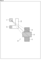
- CMOS substrate 12 As shown in FIG. 3, in the CMOS substrate 12, existing components of the CMOS substrate 12 are arranged as a shielding region 100 between the transistor 50 and the through electrode 71 when viewed in a plan view from the stacking direction.
- the shield region 100 is arranged so as to intersect with all line segments connecting the vertices of the overlap region OL, where the active region in which the source region 51/drain region 52 of the transistor 50 is formed and the gate electrode 53 overlap, and the center of the through electrode 71 (the center of gravity on the two-dimensional figure), in a plan view from the stacking direction.
- the two-dimensional shape of the overlap region OL, where the active region of the transistor 50 and the gate electrode 53 overlap, is shown as a rectangle in the example of FIG. 3, but in reality it will be a polygonal shape other than a rectangle.
- the existing components of the CMOS substrate 12 as the shield region 100, it is possible to maintain high reliability of the transistor 50 provided on the CMOS substrate 12, i.e., to reduce the effect on the transistor 50 caused by the application of a high voltage to the through electrode 71. In addition, it is possible to maintain the pixel size without providing a new member such as the shield electrode of the known example 2.
- FIG. 4 is a plan view showing a configuration example of the CMOS substrate 12 according to the first embodiment to which the technology disclosed herein is applied.
- CMOS substrate 12 in this embodiment is similar to that shown in FIG. 2, so its description is omitted.
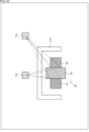
- the drain region 52 of the active region of the transistor 50 is disposed as a shield region 100 between the transistor 50 and the through electrode 71 in a plan view from the stacking direction.
- the drain region 52 is arranged so that, in plan view from the stacking direction, it intersects with all the line segments connecting the vertices of the overlapping region where the active region of the transistor 50 and the gate electrode 53 overlap with the center of the through electrode 71. This allows the effect of the electric field propagating from the through electrode 71 to be absorbed by the drain region 52.
- the drain region 52 of the active region of the transistor 50 is disposed between the transistor 50 and the through electrode 71, but the source region 51 of the active region of the transistor 50 may be disposed therebetween.
- the shape of the active region of the transistor 50 in plan view is not limited to that shown in FIG. 4. That is, for example, the drain region 52 only needs to be positioned so as to intersect with all the line segments connecting the vertices of the overlapping region where the active region of the transistor 50 and the gate electrode 53 overlap with each other in plan view from the stacking direction, and can have any shape depending on the positional relationship between the transistor 50 and the through electrode 71.
- the drain region 52 may be formed in an L-shape.
- the drain region 52 may be formed in a U-shape depending on their arrangement.
- the active region of the transistor 50 is also disposed between the transistor 50 and the through electrode 71, so it is possible to maintain the pixel size while reducing the effect on the transistor 50 of the application of a high voltage to the through electrode 71.
- FIG. 6 is a cross-sectional view showing an example of the configuration of a CMOS substrate 12 according to a second embodiment to which the technology disclosed herein is applied, and FIG. 7 is a plan view thereof.
- a substrate contact 121 and its well region 122 are formed.
- the well region 122 is an N-type or P-type diffusion layer for the substrate contact, and is fixed to a constant potential by the substrate contact 121.
- a well region 122 of a substrate contact 121 is disposed as a shield region 100 between the transistor 50 and the through electrode 71 when viewed in a plan view from the stacking direction.
- the well region 122 of the substrate contact 121 is arranged so that, in a plan view from the stacking direction, it intersects with all the line segments connecting the vertices of the overlapping region where the active region of the transistor 50 and the gate electrode 53 overlap with the center of the through electrode 71. This allows the effect of the electric field propagating from the through electrode 71 to be absorbed by the well region 122 of the substrate contact 121.
- the shape of the well region 122 of the substrate contact 121 in plan view is not limited to that shown in FIG. 7.
- the well region 122 of the substrate contact 121 only needs to be arranged so as to intersect with all the line segments connecting the vertices of the overlapping region where the active region of the transistor 50 and the gate electrode 53 overlap with each other and the center of the through electrode 71 in plan view from the stacking direction, and any shape can be adopted depending on the positional relationship between the transistor 50 and the through electrode 71.
- the well region 122 of the substrate contact 121 may be formed in an L-shape depending on the arrangement of the through electrodes 71.
- the well region 122 of the substrate contact 121 is also disposed between the transistor 50 and the through electrode 71, making it possible to maintain the pixel size while reducing the effect on the transistor 50 of the application of a high voltage to the through electrode 71.
- FIG. 9 is a cross-sectional view showing an example of the configuration of a CMOS substrate 12 according to a third embodiment to which the technology disclosed herein is applied, and FIG. 10 is a plan view thereof.
- an air gap 131 is formed in addition to the cross-sectional configuration shown in FIG. 2.
- the air gap 131 is formed, for example, by a vacuum cavity.
- air gaps 131 are arranged as shielding regions 100 between the transistor 50 and each of the two through electrodes 71a, 71b in a plan view from the stacking direction on the CMOS substrate 12.
- the air gap 131 is arranged so as to intersect with all the line segments connecting the vertices of the overlapping region where the active region of the transistor 50 and the gate electrode 53 overlap with the center of each of the through electrodes 71a and 71b when viewed in a plan view from the stacking direction. This allows the electric field from each of the through electrodes 71a and 71b to propagate while avoiding the air gap 131, which has a low dielectric constant.
- the shape of the air gap 131 in plan view is not limited to that shown in FIG. 10.
- the air gap 131 only needs to be arranged so as to intersect with all the line segments connecting the vertices of the overlapping region where the active region of the transistor 50 and the gate electrode 53 overlap with the center of the through electrode 71 (71a, 71b) in plan view from the stacking direction, and any shape can be adopted depending on the positional relationship between the transistor 50 and the through electrode 71.
- Example of distance measurement system configuration The sensor element 1 of each of the above-described embodiments can be applied to a ranging system that uses the ToF method to detect the depth distance to a subject for each pixel and captures a distance image, which is an image composed of distance pixel signals based on the detected distance.
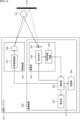
- FIG. 11 is a block diagram showing an example configuration of one embodiment of a distance measurement system 211 to which the technology disclosed herein is applied.
- the distance measurement system 211 includes an illumination device 221 and an imaging device 222.
- the lighting device 221 includes a lighting control unit 231 and a light source 232.
- the lighting control unit 231 controls the pattern in which the light source 232 irradiates light under the control of the control unit 242 of the imaging device 222. Specifically, the lighting control unit 231 controls the pattern in which the light source 232 irradiates light according to an irradiation code included in an irradiation signal supplied from the control unit 242.
- the irradiation code is composed of two values, 1 (High) and 0 (Low), and the lighting control unit 231 turns on the light source 232 when the irradiation code value is 1 and turns off the light source 232 when the irradiation code value is 0.
- the light source 232 emits light in a predetermined wavelength range under the control of the illumination control unit 231.
- the light source 232 is, for example, an infrared laser diode.
- the type of light source 232 and the wavelength range of the emitted light can be set arbitrarily depending on the application of the distance measurement system 211, etc.
- the imaging device 222 is a device that receives reflected light that is generated when light (illumination light) emitted from the lighting device 221 is reflected by the subject 212, the subject 213, etc.
- the imaging device 222 includes an imaging unit 241, a control unit 242, a display unit 243, and a storage unit 244.
- the imaging unit 241 includes a lens 251, a light receiving element 252, and a signal processing circuit 253.
- Lens 251 focuses the incident light onto the light receiving surface of light receiving element 252.
- the configuration of lens 251 is arbitrary, and for example, lens 251 can be configured with a group of multiple lenses.
- the sensor element 1 to which the technology disclosed herein is applied is applied to the light receiving element 252.
- the light receiving element 252 Under the control of the control unit 242, the light receiving element 252 receives reflected light from the subject 212, the subject 213, etc., and supplies the resulting pixel signal to the signal processing circuit 253.
- This pixel signal represents a digital count value that counts the time from when the illumination device 221 emits light to when the light receiving element 252 receives the light.
- An emission timing signal that indicates the timing at which the light source 232 emits light is also supplied from the control unit 242 to the light receiving element 252.
- the signal processing circuit 253 processes the pixel signal supplied from the light receiving element 252 under the control of the control unit 242. For example, the signal processing circuit 253 detects the distance to the subject for each pixel based on the pixel signal supplied from the light receiving element 252, and generates a distance image showing the distance to the subject for each pixel. Specifically, the signal processing circuit 253 acquires the time (count value) from when the light source 232 emits light to when each pixel of the light receiving element 252 receives the light multiple times (for example, thousands to tens of thousands of times) for each pixel. The signal processing circuit 253 creates a histogram corresponding to the acquired time.
- the signal processing circuit 253 detects the peak of the histogram to determine the time until the light irradiated from the light source 232 is reflected by the subject 212 or the subject 213 and returns. Furthermore, the signal processing circuit 253 performs a calculation to obtain the distance to the object based on the determined time and the speed of light. The signal processing circuit 253 supplies the generated distance image to the control unit 242.
- the control unit 242 is composed of a control circuit and a processor, such as an FPGA (Field Programmable Gate Array) and a DSP (Digital Signal Processor).
- the control unit 242 controls the illumination control unit 231 and the light receiving element 252. Specifically, the control unit 242 supplies an irradiation signal to the illumination control unit 231 and a light emission timing signal to the light receiving element 252.
- the light source 232 emits irradiation light in response to the irradiation signal.
- the light emission timing signal may be the irradiation signal supplied to the illumination control unit 231.
- the control unit 242 also causes the display unit 243 to display the distance image acquired from the imaging unit 241. Furthermore, the control unit 242 causes the memory unit 244 to store the distance image acquired from the imaging unit 241. Furthermore, the control unit 242 outputs the distance image acquired from the imaging unit 241 to the outside.
- the display unit 243 is, for example, a panel-type display device such as a liquid crystal display device or an organic EL (Electro Luminescence) display device.
- a panel-type display device such as a liquid crystal display device or an organic EL (Electro Luminescence) display device.
- the storage unit 244 can be configured from any storage device or storage medium, and stores distance images, etc.
- the distance measurement system 211 configured in this manner, by applying the sensor element 1 to which the technology disclosed herein is applied, it is possible to achieve, for example, further miniaturization and higher functionality.
- CMOS complementary metal oxide semiconductor
- a first conductive type transistor and a second conductive type transistor are provided on the CMOS substrate;
- the element isolation region is formed by a deep trench isolation (DTI) region penetrating the CMOS substrate from a surface to a bottom surface.
- DTI deep trench isolation
- an STI Shallow Trench Isolation
- An illumination device that emits irradiation light; a sensor element for detecting reflected light of the irradiated light,
- the sensor element includes: A sensor substrate on which a single photon avalanche diode (SPAD) is provided for each pixel; a complementary metal oxide semiconductor (CMOS) substrate on which a transistor for reading out a signal is provided and which is laminated on the sensor substrate; a logic substrate laminated on the CMOS substrate and provided with a logic circuit; a through electrode penetrating the CMOS substrate and electrically connecting the sensor substrate and the CMOS substrate.
- CMOS complementary metal oxide semiconductor
Landscapes
- Solid State Image Pick-Up Elements (AREA)
- Metal-Oxide And Bipolar Metal-Oxide Semiconductor Integrated Circuits (AREA)
- Semiconductor Integrated Circuits (AREA)
Abstract
本開示は、画素サイズを維持しつつ、さらなる高機能化を図ることができるようにするセンサ素子および測距システムに関する。 本開示のセンサ素子は、SPADが画素毎に設けられたセンサ基板と、センサ基板に積層され、信号の読み出しのためのトランジスタが設けられるCMOS基板と、CMOS基板に積層され、ロジック回路が設けられたロジック基板と、CMOS基板を貫通し、センサ基板のアノード領域とCMOS基板とを電気的に接続する貫通電極とを備える。本開示は、例えばCMOSイメージセンサに適用することができる。
Description
本開示は、センサ素子および測距システムに関し、特に、画素サイズを維持しつつ、さらなる高機能化を図ることができるようにするセンサ素子および測距システムに関する。
ToF(Time-of-Flight)法により距離計測を行う距離画像センサが知られている。距離画像センサでは、例えば、SPAD(Single Photon Avalanche Diode)を用いた画素を行列状に配置した画素アレイが採用される。SPADでは、降伏電圧よりも大きい電圧を印加した状態で、高電界のPN接合領域へ1個の光子が入ると、アバランシェ増幅が発生する。その際の瞬間的に電流が流れたタイミングを検出することで、高精度に距離を計測することができる。
従来、SPADを利用した測距システムでは、SPADが設けられたセンサ基板とロジック回路が設けられたロジック基板とが貼り合された積層構造で、半導体基板の裏面側から光が照射される裏面照射型のセンサ素子が採用されている。
特許文献1には、積層構造のセンサ素子において、小型化かつ高機能化を図るために、SPADのカソード電圧またはアノード電圧に従った信号を出力するための複数のトランジスタの一部を、センサ基板の半導体基板に形成されたウェル内に設けることが提案されている。
近年、積層構造のセンサ素子においては、ロジック回路のさらなる高機能化が求められている。しかしながら、特許文献1に開示されているような2層構造のセンサ素子において、画素サイズを維持したまま、ロジック回路における演算のためのSRAM(Static Random Access Memory)などを増設することは容易ではなかった。
本開示は、このような状況に鑑みてなされたものであり、画素サイズを維持しつつ、さらなる高機能化を図ることができるようにするものである。
本開示のセンサ素子は、SPAD(Single Photon Avalanche Diode)が画素毎に設けられたセンサ基板と、前記センサ基板に積層され、信号の読み出しのためのトランジスタが設けられるCMOS(Complementary Metal Oxide Semiconductor)基板と、前記CMOS基板に積層され、ロジック回路が設けられたロジック基板と、前記CMOS基板を貫通し、前記センサ基板のアノード領域と前記CMOS基板とを電気的に接続する貫通電極とを備えるセンサ素子である。
本開示の測距システムは、照射光を照射する照明装置と、前記照射光に対する反射光を検出するセンサ素子とを備え、前記センサ素子は、SPAD(Single Photon Avalanche Diode)が画素毎に設けられたセンサ基板と、前記センサ基板に積層され、信号の読み出しのためのトランジスタが設けられるCMOS(Complementary Metal Oxide Semiconductor)基板と、前記CMOS基板に積層され、ロジック回路が設けられたロジック基板と、前記CMOS基板を貫通し、前記センサ基板のアノード領域と前記CMOS基板とを電気的に接続する貫通電極とを有する測距システムである。
本開示においては、SPADが画素毎に設けられたセンサ基板と、前記センサ基板に積層され、信号の読み出しのためのトランジスタが設けられるCMOS基板と、前記CMOS基板に積層され、ロジック回路が設けられたロジック基板と、前記CMOS基板を貫通し、前記センサ基板のアノード領域と前記CMOS基板とを電気的に接続する貫通電極が設けられる。
以下、本開示を実施するための形態(以下、実施形態とする)について説明する。なお、説明は以下の順序で行う。
1.従来技術とその問題点
2.本開示に係る技術を適用したセンサ素子の構成例
3.第1の実施形態(ソース領域/ドレイン領域をシールド領域とする構成)
4.第2の実施形態(基板コンタクトのウェル領域をシールド領域とする構成)
5.第3の実施形態(エアギャップをシールド領域とする構成)
6.測距システムの構成例
2.本開示に係る技術を適用したセンサ素子の構成例
3.第1の実施形態(ソース領域/ドレイン領域をシールド領域とする構成)
4.第2の実施形態(基板コンタクトのウェル領域をシールド領域とする構成)
5.第3の実施形態(エアギャップをシールド領域とする構成)
6.測距システムの構成例
<1.従来技術とその問題点>
従来、SPAD(Single Photon Avalanche Diode)を利用した測距システムでは、SPADが設けられたセンサ基板とロジック回路が設けられたロジック基板とが貼り合された積層構造で、半導体基板の裏面側から光が照射される裏面照射型のセンサ素子が採用されている。
従来、SPAD(Single Photon Avalanche Diode)を利用した測距システムでは、SPADが設けられたセンサ基板とロジック回路が設けられたロジック基板とが貼り合された積層構造で、半導体基板の裏面側から光が照射される裏面照射型のセンサ素子が採用されている。
特許文献1(特開2022-148028号公報)には、積層構造のセンサ素子において、小型化かつ高機能化を図るために、SPADのカソード電圧またはアノード電圧に従った信号を出力するための複数のトランジスタの一部を、センサ基板の半導体基板に形成されたウェル内に設けることが提案されている。
近年、積層構造のセンサ素子においては、ロジック回路のさらなる高機能化が求められている。しかしながら、特許文献1に開示されているような2層構造のセンサ素子において、画素サイズを維持したまま、ロジック回路における演算のためのSRAM(Static Random Access Memory)などを増設することは容易ではなかった。
そこで、本開示に係る技術においては、SPADが画素毎に設けられたセンサ基板と、ロジック回路が設けられたロジック基板との間に、信号の読み出しのためのトランジスタが設けられるCMOS(Complementary Metal Oxide Semiconductor)基板を積層することで、ロジック回路の面積を確保することを実現する。
一方で、このような3層構造のセンサ素子においては、CMOS基板を貫通するアノード電極に-20乃至-25Vの高電圧が印加されるため、CMOS基板に設けられるトランジスタのON-OFF特性への影響が懸念される。
これに対して、国際公開第2020/262558号(公知例2という)には、第1基板のフローティングディフュージョンと第2基板の画素回路とを電気的に接続する貫通電極と、画素回路を構成する各トランジスタとの間に、シールド電極を設けるようにした撮像装置が開示されている。シールド電極は、画素回路を構成する各トランジスタに対する、貫通配線に印加されるバイアスの影響を低減するためのものである。
しかしながら、公知例2では、画素サイズの縮小については考慮されておらず、面積効率の観点で課題があった。
そこで、本開示に係る技術においては、CMOS基板において、積層方向からの平面視で、トランジスタと貫通電極との間に、CMOS基板の既存構成要素をシールド領域として配置することで、シールド電極のような新たな部材を設けることなく、画素サイズを維持することを実現する。
<2.本開示に係る技術を適用したセンサ素子の構成例>
図1乃至図3を参照して、本開示に係る技術を適用したセンサ素子の構成について説明する。
図1乃至図3を参照して、本開示に係る技術を適用したセンサ素子の構成について説明する。
図1は、本開示に係る技術を適用したセンサ素子1が有する画素10の断面的な構成例の一例を示している。
センサ素子1は、例えば、CMOSイメージセンサなどとして構成される。図1に示されるように、センサ素子1は、画素10毎にSPAD31が設けられたセンサ基板11、センサ基板11に積層され、信号の読み出しのためのトランジスタが設けられるCMOS基板12、および、CMOS基板12に積層され、ロジック回路が設けられたロジック基板13からなる3層構造を有する。センサ基板11は、半導体基板21の上面(裏面)に対してオンチップレンズ層22が積層されて構成される。ロジック基板13は、半導体基板23の上面に対して配線層24が積層されて構成される。オンチップレンズ層22には、画素10毎にマイクロレンズ25が設けられる。
画素10は、半導体基板21のウェル層32が画素分離部33によって隣接する他の画素10のウェル層32と電気的に分離されて構成される。また、図示はしないが、画素10には、ウェル層32の側面と上面を囲うように、ホールを蓄積するためのP型半導体領域が設けられる。そのP型半導体領域が形成される領域に対応する半導体基板21の下面側には、P型半導体領域よりもP型の不純物濃度が高いアノード領域34が形成される。
画素10において、半導体基板21の下面側には、N型増倍領域とP型増倍領域のPN接合領域によりSPAD31が構成されている。SPAD31は、画素10に光が入射したのに応じて発生する電子がアバランシェ増幅されることで流れる電流によってカソード電位が降下するフォトダイオードである。また、SPAD31において、PN接合を形成するN型増倍領域には、N型増倍領域よりも不純物濃度が高いN型の不純物濃度が高いカソード領域35が形成される。
CMOS基板12には、SPAD31のカソード電圧に従った信号の読み出しのためのトランジスタ50とトランジスタ60が設けられる。トランジスタ50とトランジスタ60は、それぞれ異なる伝導型のトランジスタで構成される。トランジスタ50とトランジスタ60の一方は、PMOSトランジスタで構成され、トランジスタ50とトランジスタ60の他方は、NMOSトランジスタで構成されればよい。
例えば、トランジスタ50がPMOSトランジスタで構成される場合、Nウェルに対して設けられるP型領域であるソース領域51とドレイン領域52の間に、酸化膜などの絶縁膜を介して積層するようにゲート電極53が設けられて構成される。同様に、トランジスタ60がNMOSトランジスタで構成される場合、Pウェルに対して設けられるN型領域であるソース領域61とドレイン領域62の間に、酸化膜などの絶縁膜を介して積層するようにゲート電極63が設けられて構成される。
トランジスタ50とトランジスタ60は、プレナー構造のトランジスタとして構成されるものとするが、これに限らず、トレンチ構造のトランジスタとして構成されてもよい。
CMOS基板12には、CMOS基板12を貫通し、センサ基板11とCMOS基板12とを電気的に接続する貫通電極71,72が設けられる。
貫通電極71は、センサ基板11に形成されるアノード領域34とCMOS基板12に設けられる各トランジスタとを、ロジック基板13に形成される図示せぬSPAD回路を介して接続するアノード電極として形成される。また、貫通電極72は、SPAD31のN型増倍領域に形成されるカソード領域35とCMOS基板12に設けられる各トランジスタとを、ロジック基板13に形成される図示せぬSPAD回路を介して接続するカソード電極として形成される。
以上のように、SPAD31が画素10毎に設けられたセンサ基板11と、ロジック回路が設けられたロジック基板13との間に、信号の読み出しのためのトランジスタ50,60が設けられるCMOS基板12を積層することで、ロジック回路の面積を確保することが可能となる。すなわち、画素サイズを維持しつつ、ロジック回路における演算のためのSRAMなどを増設することができ、センサ素子1のさらなる高機能化を実現することが可能となる。
図2を参照して、CMOS基板12の詳細な構成について説明する。
図2には、CMOS基板12においてトランジスタ50が設けられている一部領域の断面が示されている。なお、図2に示される断面構成は、図1に示される断面構成を上下反転したものである。
CMOS基板12において、トランジスタ50と貫通電極71との間には、素子分離領域81が形成されている。素子分離領域81は、例えば、Si酸化膜などの絶縁膜で形成された深さ250nm程度のSTI(Shallow Trench Isolation)領域、または、CMOS基板12のSi表面から底面までを貫通するSi酸化膜などで形成されたDTI(Deep Trench Isolation)領域などとして形成されるが、イオン注入により形成されてもよい。
また、互いに異なる伝導型トランジスタ50とトランジスタ60(不図示)との間には、素子分離領域82が形成される。素子分離領域82は、例えば、CMOS基板12のSi表面から底面までを貫通するSi酸化膜などで形成されたDTI領域などとして形成されるが、イオン注入により形成されてもよい。
さて、アノード領域34に接続される貫通電極71には、絶対値20V以上の電圧が印加される。具体的には、貫通電極71には、-20乃至-25Vの高電圧が印加される。そのため、CMOS基板12に設けられる各トランジスタのON-OFF特性への影響が懸念される。
そこで、図3に示されるように、CMOS基板12において、積層方向からの平面視で、トランジスタ50と貫通電極71との間に、CMOS基板12の既存構成要素をシールド領域100として配置する。
シールド領域100は、積層方向からの平面視で、トランジスタ50のソース領域51/ドレイン領域52が形成されるアクティブ領域とゲート電極53とが重なる重複領域OLの頂点それぞれと、貫通電極71の中心(2次元図形上の重心)とを結ぶ全ての線分と交差するように配置されるものとする。トランジスタ50のアクティブ領域とゲート電極53とが重なって形成される重複領域OLの2次元形状は、図3の例では矩形で示されているが、実際には矩形以外の多角形などの形状となる。
以上のように、CMOS基板12の既存構成要素をシールド領域100として配置することで、CMOS基板12に設けられるトランジスタ50の高い信頼性を保つこと、すなわち、貫通電極71に高電圧が印加されることによるトランジスタ50への影響を低減することが可能となる。また、公知例2のシールド電極のような新たな部材を設けることなく、画素サイズを維持することが可能となる。
以下では、シールド領域100として配置されるCMOS基板12の既存構成要素の具体例について説明する。
<3.第1の実施形態>
図4は、本開示に係る技術を適用した第1の実施形態のCMOS基板12の構成例を示す平面図である。
図4は、本開示に係る技術を適用した第1の実施形態のCMOS基板12の構成例を示す平面図である。
なお、本実施形態のCMOS基板12の断面構成は、図2に示される断面構成と同様であるので、その説明は省略する。
図4の例では、CMOS基板12において、積層方向からの平面視で、トランジスタ50と貫通電極71との間に、シールド領域100として、トランジスタ50のアクティブ領域のうちのドレイン領域52が配置される。
ドレイン領域52は、積層方向からの平面視で、トランジスタ50のアクティブ領域とゲート電極53とが重なる重複領域の頂点それぞれと、貫通電極71の中心とを結ぶ全ての線分と交差するように配置されるものとする。これにより、貫通電極71から伝播する電界の影響が、ドレイン領域52に吸収されるようになる。
以上のように、トランジスタ50と貫通電極71との間に、トランジスタ50のアクティブ領域を配置することで、貫通電極71に高電圧が印加されることによるトランジスタ50への影響を低減しつつ、画素サイズを維持することが可能となる。
なお、図4の例では、トランジスタ50と貫通電極71との間に、トランジスタ50のアクティブ領域のうちのドレイン領域52が配置されるものとしたが、トランジスタ50のアクティブ領域のうちのソース領域51が配置されるようにしてもよい。
また、トランジスタ50のアクティブ領域の平面視での形状は、図4に示されるものに限られない。すなわち、例えばドレイン領域52は、積層方向からの平面視で、トランジスタ50のアクティブ領域とゲート電極53とが重なる重複領域の頂点それぞれと、貫通電極71の中心とを結ぶ全ての線分と交差するように配置されればよく、トランジスタ50と貫通電極71の位置関係に応じて、任意の形状を採ることができる。
例えば、図5のA図に示されるように、貫通電極71が、トランジスタ50のアクティブ領域の長手方向の延長線上に設けられていない場合には、ドレイン領域52(またはソース領域51)がL字型に形成されるようにしてもよい。
また、同B図に示されるように、2つの貫通電極71a,71bが設けられている場合には、それらの配置に応じて、ドレイン領域52(またはソース領域51)がコの字型に形成されてもよい。
図5の例においても、トランジスタ50と貫通電極71との間に、トランジスタ50のアクティブ領域が配置されるので、貫通電極71に高電圧が印加されることによるトランジスタ50への影響を低減しつつ、画素サイズを維持することが可能となる。
<4.第2の実施形態>
図6は、本開示に係る技術を適用した第2の実施形態のCMOS基板12の構成例を示す断面図であり、図7は、その平面図である。
図6は、本開示に係る技術を適用した第2の実施形態のCMOS基板12の構成例を示す断面図であり、図7は、その平面図である。
図6に示される断面構成においては、図2に示される断面構成に加え、基板コンタクト121とそのウェル領域122が形成されている。ウェル領域122は、基板コンタクト用のN型またはP型の拡散層であり、基板コンタクト121によって一定の電位に固定されている。
そして、図7の例では、CMOS基板12において、積層方向からの平面視で、トランジスタ50と貫通電極71との間に、シールド領域100として、基板コンタクト121のウェル領域122が配置される。
基板コンタクト121のウェル領域122は、積層方向からの平面視で、トランジスタ50のアクティブ領域とゲート電極53とが重なる重複領域の頂点それぞれと、貫通電極71の中心とを結ぶ全ての線分と交差するように配置されるものとする。これにより、貫通電極71から伝播する電界の影響が、基板コンタクト121のウェル領域122に吸収されるようになる。
以上のように、トランジスタ50と貫通電極71との間に、基板コンタクト121のウェル領域122を配置することで、貫通電極71に高電圧が印加されることによるトランジスタ50への影響を低減しつつ、画素サイズを維持することが可能となる。
また、基板コンタクト121のウェル領域122の平面視での形状は、図7に示されるものに限られない。すなわち、基板コンタクト121のウェル領域122が、積層方向からの平面視で、トランジスタ50のアクティブ領域とゲート電極53とが重なる重複領域の頂点それぞれと、貫通電極71の中心とを結ぶ全ての線分と交差するように配置されればよく、トランジスタ50と貫通電極71の位置関係に応じて、任意の形状を採ることができる。
例えば、図8に示されるように、貫通電極71の配置に応じて、基板コンタクト121のウェル領域122がL字型に形成されるようにしてもよい。
図8の例においても、トランジスタ50と貫通電極71との間に、基板コンタクト121のウェル領域122が配置されるので、貫通電極71に高電圧が印加されることによるトランジスタ50への影響を低減しつつ、画素サイズを維持することが可能となる。
<5.第3の実施形態>
図9は、本開示に係る技術を適用した第3の実施形態のCMOS基板12の構成例を示す断面図であり、図10は、その平面図である。
図9は、本開示に係る技術を適用した第3の実施形態のCMOS基板12の構成例を示す断面図であり、図10は、その平面図である。
図9に示される断面構成においては、図2に示される断面構成に加え、エアギャップ131が形成されている。エアギャップ131は、例えば、真空の空洞で構成される。
そして、図10の例では、CMOS基板12において、積層方向からの平面視で、トランジスタ50と2つの貫通電極71a,71bそれぞれとの間に、シールド領域100として、エアギャップ131が配置される。
エアギャップ131は、積層方向からの平面視で、トランジスタ50のアクティブ領域とゲート電極53とが重なる重複領域の頂点それぞれと、貫通電極71a,71bそれぞれの中心とを結ぶ全ての線分と交差するように配置されるものとする。これにより、貫通電極71a,71bそれぞれからの電界は、誘電率の低いエアギャップ131を避けて伝播するようになる。
以上の構成によれば、トランジスタ50と貫通電極71a,71bそれぞれとの間に、エアギャップ131を配置することで、貫通電極71に高電圧が印加されることによるトランジスタ50への影響を低減しつつ、画素サイズを維持することが可能となる。
また、エアギャップ131の平面視での形状は、図10に示されるものに限られない。すなわち、エアギャップ131が、積層方向からの平面視で、トランジスタ50のアクティブ領域とゲート電極53とが重なる重複領域の頂点それぞれと、貫通電極71(71a,71b)の中心とを結ぶ全ての線分と交差するように配置されればよく、トランジスタ50と貫通電極71の位置関係に応じて、任意の形状を採ることができる。
<6.測距システムの構成例>
上述したような各実施形態のセンサ素子1は、ToF法を用いて、被写体までの奥行き方向の距離を画素毎に検出し、検出した距離に基づく距離画素信号からなる画像である距離画像の撮像を行う測距システムに適用することができる。
上述したような各実施形態のセンサ素子1は、ToF法を用いて、被写体までの奥行き方向の距離を画素毎に検出し、検出した距離に基づく距離画素信号からなる画像である距離画像の撮像を行う測距システムに適用することができる。
図11は、本開示に係る技術を適用した測距システム211の一実施形態の構成例を示すブロック図である。
図11に示されるように、測距システム211は、照明装置221と撮像装置222を備える。
照明装置221は、照明制御部231と光源232を備える。
照明制御部231は、撮像装置222の制御部242の制御の下、光源232が光を照射するパターンを制御する。具体的には、照明制御部231は、制御部242から供給される照射信号に含まれる照射コードに従って、光源232が光を照射するパターンを制御する。例えば、照射コードは、1(High)と0(Low)の2値からなり、照明制御部231は、照射コードの値が1のときに光源232を点灯させ、照射コードの値が0のときに光源232を消灯させる。
光源232は、照明制御部231の制御の下、所定の波長域の光を発する。光源232は、例えば、赤外線レーザダイオードからなる。光源232の種類と、照射光の波長域は、測距システム211の用途などに応じて任意に設定することが可能である。
撮像装置222は、照明装置221から照射された光(照射光)が被写体212や被写体213などにより反射された反射光を受光する装置である。撮像装置222は、撮像部241、制御部242、表示部243、および記憶部244を備える。
撮像部241は、レンズ251、受光素子252、および信号処理回路253を備える。
レンズ251は、入射光を受光素子252の受光面に結像させる。レンズ251の構成は任意であり、例えば、複数のレンズ群によりレンズ251を構成することも可能である。
受光素子252には、本開示に係る技術を適用したセンサ素子1が適用される。受光素子252は、制御部242の制御の下、被写体212や被写体213などからの反射光を受光し、その結果得られた画素信号を信号処理回路253に供給する。この画素信号は、照明装置221が照射光を照射してから、受光素子252が受光するまでの時間をカウントしたデジタルのカウント値を表す。光源232が発光するタイミングを示す発光タイミング信号は、制御部242から受光素子252にも供給される。
信号処理回路253は、制御部242の制御の下、受光素子252から供給される画素信号の処理を行う。例えば、信号処理回路253は、受光素子252から供給される画素信号に基づいて、画素毎に被写体までの距離を検出し、画素毎の被写体までの距離を示す距離画像を生成する。具体的には、信号処理回路253は、光源232が光を発光してから受光素子252の各画素が光を受光するまでの時間(カウント値)を画素毎に複数回(例えば、数千乃至数万回)取得する。信号処理回路253は、取得した時間に対応するヒストグラムを作成する。そして、信号処理回路253は、ヒストグラムのピークを検出することで、光源232から照射された光が被写体212や被写体213で反射して戻ってくるまでの時間を判定する。さらに、信号処理回路253は、判定した時間と光速に基づいて、物体までの距離を求める演算を行う。信号処理回路253は、生成した距離画像を制御部242に供給する。
制御部242は、例えば、FPGA(Field Programmable Gate Array),DSP(Digital Signal Processor)などの制御回路やプロセッサなどにより構成される。制御部242は、照明制御部231と受光素子252の制御を行う。具体的には、制御部242は、照明制御部231に照射信号を供給するとともに、発光タイミング信号を受光素子252に供給する。光源232は、照射信号に応じて照射光を発光する。発光タイミング信号は、照明制御部231に供給される照射信号でもよい。また、制御部242は、撮像部241から取得した距離画像を表示部243に表示させる。さらに、制御部242は、撮像部241から取得した距離画像を記憶部244に記憶させる。また、制御部242は、撮像部241から取得した距離画像を外部に出力する。
表示部243は、例えば、液晶表示装置や有機EL(Electro Luminescence)表示装置などのパネル型表示装置からなる。
記憶部244は、任意の記憶装置や記憶媒体などにより構成することができ、距離画像などを記憶する。
このように構成されている測距システム211では、本開示に係る技術を適用したセンサ素子1を適用することで、例えば、より小型化かつ高機能化を図ることができる。
本明細書において、システムとは、複数の構成要素(装置、モジュール(部品)等)の集合を意味し、すべての構成要素が同一筐体中にあるか否かは問わない。したがって、別個の筐体に収納され、ネットワークを介して接続されている複数の装置、及び、1つの筐体の中に複数のモジュールが収納されている1つの装置は、いずれも、システムである。
本明細書に記載された効果はあくまで例示であって限定されるものではなく、他の効果があってもよい。
また、本開示に係る技術を適用した実施形態は、上述した実施形態に限定されるものではなく、本開示に係る技術の要旨を逸脱しない範囲において種々の変更が可能である。
さらに、本開示は以下のような構成をとることができる。
(1)
SPAD(Single Photon Avalanche Diode)が画素毎に設けられたセンサ基板と、
前記センサ基板に積層され、信号の読み出しのためのトランジスタが設けられるCMOS(Complementary Metal Oxide Semiconductor)基板と、
前記CMOS基板に積層され、ロジック回路が設けられたロジック基板と、
前記CMOS基板を貫通し、前記センサ基板と前記CMOS基板とを電気的に接続する貫通電極と
を備えるセンサ素子。
(2)
前記CMOS基板において、積層方向からの平面視で、前記トランジスタと前記貫通電極との間に、前記CMOS基板の既存構成要素がシールド領域として配置される
(1)に記載のセンサ素子。
(3)
前記シールド領域は、積層方向からの平面視で、前記トランジスタのアクティブ領域とゲート電極とが重なる重複領域の頂点それぞれと、前記貫通電極の中心とを結ぶ全ての線分と交差するように配置される
(2)に記載のセンサ素子。
(4)
前記シールド領域は、前記トランジスタの前記アクティブ領域のソース領域またはドレイン領域である
(3)に記載のセンサ素子。
(5)
前記シールド領域は、基板コンタクトのウェル領域である
(3)に記載のセンサ素子。
(6)
前記シールド領域は、エアギャップである
(3)に記載のセンサ素子。
(7)
前記貫通電極には、絶対値20V以上の電圧が印加される
(3)乃至(6)のいずれかに記載のセンサ素子。
(8)
前記CMOS基板には、第1伝導型トランジスタと第2伝導型トランジスタが設けられ、
前記第1伝導型トランジスタと前記第2伝導型トランジスタとの間には、素子分離領域が形成される
(3)乃至(7)のいずれかに記載のセンサ素子。
(9)
前記素子分離領域は、前記CMOS基板の表面から底面までを貫通するDTI(Deep Trench Isolation)領域により形成される
(8)に記載のセンサ素子。
(10)
前記CMOS基板において、前記トランジスタと前記貫通電極との間には、深さ250nm程度のSTI(Shallow Trench Isolation)領域または前記DTI領域がさらに形成される
(9)に記載のセンサ素子。
(11)
照射光を照射する照明装置と、
前記照射光に対する反射光を検出するセンサ素子と
を備え、
前記センサ素子は、
SPAD(Single Photon Avalanche Diode)が画素毎に設けられたセンサ基板と、 前記センサ基板に積層され、信号の読み出しのためのトランジスタが設けられるCMOS(Complementary Metal Oxide Semiconductor)基板と、
前記CMOS基板に積層され、ロジック回路が設けられたロジック基板と、
前記CMOS基板を貫通し、前記センサ基板と前記CMOS基板とを電気的に接続する貫通電極とを有する
測距システム。
(1)
SPAD(Single Photon Avalanche Diode)が画素毎に設けられたセンサ基板と、
前記センサ基板に積層され、信号の読み出しのためのトランジスタが設けられるCMOS(Complementary Metal Oxide Semiconductor)基板と、
前記CMOS基板に積層され、ロジック回路が設けられたロジック基板と、
前記CMOS基板を貫通し、前記センサ基板と前記CMOS基板とを電気的に接続する貫通電極と
を備えるセンサ素子。
(2)
前記CMOS基板において、積層方向からの平面視で、前記トランジスタと前記貫通電極との間に、前記CMOS基板の既存構成要素がシールド領域として配置される
(1)に記載のセンサ素子。
(3)
前記シールド領域は、積層方向からの平面視で、前記トランジスタのアクティブ領域とゲート電極とが重なる重複領域の頂点それぞれと、前記貫通電極の中心とを結ぶ全ての線分と交差するように配置される
(2)に記載のセンサ素子。
(4)
前記シールド領域は、前記トランジスタの前記アクティブ領域のソース領域またはドレイン領域である
(3)に記載のセンサ素子。
(5)
前記シールド領域は、基板コンタクトのウェル領域である
(3)に記載のセンサ素子。
(6)
前記シールド領域は、エアギャップである
(3)に記載のセンサ素子。
(7)
前記貫通電極には、絶対値20V以上の電圧が印加される
(3)乃至(6)のいずれかに記載のセンサ素子。
(8)
前記CMOS基板には、第1伝導型トランジスタと第2伝導型トランジスタが設けられ、
前記第1伝導型トランジスタと前記第2伝導型トランジスタとの間には、素子分離領域が形成される
(3)乃至(7)のいずれかに記載のセンサ素子。
(9)
前記素子分離領域は、前記CMOS基板の表面から底面までを貫通するDTI(Deep Trench Isolation)領域により形成される
(8)に記載のセンサ素子。
(10)
前記CMOS基板において、前記トランジスタと前記貫通電極との間には、深さ250nm程度のSTI(Shallow Trench Isolation)領域または前記DTI領域がさらに形成される
(9)に記載のセンサ素子。
(11)
照射光を照射する照明装置と、
前記照射光に対する反射光を検出するセンサ素子と
を備え、
前記センサ素子は、
SPAD(Single Photon Avalanche Diode)が画素毎に設けられたセンサ基板と、 前記センサ基板に積層され、信号の読み出しのためのトランジスタが設けられるCMOS(Complementary Metal Oxide Semiconductor)基板と、
前記CMOS基板に積層され、ロジック回路が設けられたロジック基板と、
前記CMOS基板を貫通し、前記センサ基板と前記CMOS基板とを電気的に接続する貫通電極とを有する
測距システム。
1 センサ素子, 10 画素, 11 センサ基板, 12 CMOS基板, 13 ロジック基板, 31 SPAD, 34 アノード領域, 35 カソード領域, 50 トランジスタ, 51 ソース領域, 52 ドレイン領域, 53 ゲート電極, 60 トランジスタ, 61 ソース領域, 62 ドレイン領域, 63 ゲート電極, 71,72 貫通電極, 81,82 素子分離領域, 100 シールド領域, 121 基板コンタクト , 122 ウェル領域, 131 エアギャップ
Claims (11)
- SPAD(Single Photon Avalanche Diode)が画素毎に設けられたセンサ基板と、
前記センサ基板に積層され、信号の読み出しのためのトランジスタが設けられるCMOS(Complementary Metal Oxide Semiconductor)基板と、
前記CMOS基板に積層され、ロジック回路が設けられたロジック基板と、
前記CMOS基板を貫通し、前記センサ基板のアノード領域と前記CMOS基板とを電気的に接続する貫通電極と
を備えるセンサ素子。 - 前記CMOS基板において、積層方向からの平面視で、前記トランジスタと前記貫通電極との間に、前記CMOS基板の既存構成要素がシールド領域として配置される
請求項1に記載のセンサ素子。 - 前記シールド領域は、積層方向からの平面視で、前記トランジスタのアクティブ領域とゲート電極とが重なる重複領域の頂点それぞれと、前記貫通電極の中心とを結ぶ全ての線分と交差するように配置される
請求項2に記載のセンサ素子。 - 前記シールド領域は、前記トランジスタの前記アクティブ領域のソース領域またはドレイン領域である
請求項3に記載のセンサ素子。 - 前記シールド領域は、基板コンタクトのウェル領域である
請求項3に記載のセンサ素子。 - 前記シールド領域は、エアギャップである
請求項3に記載のセンサ素子。 - 前記貫通電極には、絶対値20V以上の電圧が印加される
請求項3に記載のセンサ素子。 - 前記CMOS基板には、第1伝導型トランジスタと第2伝導型トランジスタが設けられ、
前記第1伝導型トランジスタと前記第2伝導型トランジスタとの間には、素子分離領域が形成される
請求項3に記載のセンサ素子。 - 前記素子分離領域は、前記CMOS基板の表面から底面までを貫通するDTI(Deep Trench Isolation)領域により形成される
請求項8に記載のセンサ素子。 - 前記CMOS基板において、前記トランジスタと前記貫通電極との間には、深さ250nm程度のSTI(Shallow Trench Isolation)領域または前記DTI領域がさらに形成される
請求項9に記載のセンサ素子。 - 照射光を照射する照明装置と、
前記照射光に対する反射光を検出するセンサ素子と
を備え、
前記センサ素子は、
SPAD(Single Photon Avalanche Diode)が画素毎に設けられたセンサ基板と、 前記センサ基板に積層され、信号の読み出しのためのトランジスタが設けられるCMOS(Complementary Metal Oxide Semiconductor)基板と、
前記CMOS基板に積層され、ロジック回路が設けられたロジック基板と、
前記CMOS基板を貫通し、前記センサ基板のアノード領域と前記CMOS基板とを電気的に接続する貫通電極とを有する
測距システム。
Priority Applications (1)
| Application Number | Priority Date | Filing Date | Title |
|---|---|---|---|
| CN202480033008.XA CN121153355A (zh) | 2023-07-04 | 2024-06-18 | 传感器元件和距离测量系统 |
Applications Claiming Priority (2)
| Application Number | Priority Date | Filing Date | Title |
|---|---|---|---|
| JP2023109745A JP2025007974A (ja) | 2023-07-04 | 2023-07-04 | センサ素子および測距システム |
| JP2023-109745 | 2023-07-04 |
Publications (1)
| Publication Number | Publication Date |
|---|---|
| WO2025009376A1 true WO2025009376A1 (ja) | 2025-01-09 |
Family
ID=94172031
Family Applications (1)
| Application Number | Title | Priority Date | Filing Date |
|---|---|---|---|
| PCT/JP2024/021970 Ceased WO2025009376A1 (ja) | 2023-07-04 | 2024-06-18 | センサ素子および測距システム |
Country Status (3)
| Country | Link |
|---|---|
| JP (1) | JP2025007974A (ja) |
| CN (1) | CN121153355A (ja) |
| WO (1) | WO2025009376A1 (ja) |
Citations (3)
| Publication number | Priority date | Publication date | Assignee | Title |
|---|---|---|---|---|
| JP2019033136A (ja) * | 2017-08-04 | 2019-02-28 | ソニーセミコンダクタソリューションズ株式会社 | 固体撮像素子 |
| WO2020262558A1 (ja) * | 2019-06-26 | 2020-12-30 | ソニーセミコンダクタソリューションズ株式会社 | 撮像装置 |
| JP2021002542A (ja) * | 2019-06-19 | 2021-01-07 | ソニーセミコンダクタソリューションズ株式会社 | アバランシェフォトダイオードセンサ及び測距装置 |
-
2023
- 2023-07-04 JP JP2023109745A patent/JP2025007974A/ja active Pending
-
2024
- 2024-06-18 CN CN202480033008.XA patent/CN121153355A/zh active Pending
- 2024-06-18 WO PCT/JP2024/021970 patent/WO2025009376A1/ja not_active Ceased
Patent Citations (3)
| Publication number | Priority date | Publication date | Assignee | Title |
|---|---|---|---|---|
| JP2019033136A (ja) * | 2017-08-04 | 2019-02-28 | ソニーセミコンダクタソリューションズ株式会社 | 固体撮像素子 |
| JP2021002542A (ja) * | 2019-06-19 | 2021-01-07 | ソニーセミコンダクタソリューションズ株式会社 | アバランシェフォトダイオードセンサ及び測距装置 |
| WO2020262558A1 (ja) * | 2019-06-26 | 2020-12-30 | ソニーセミコンダクタソリューションズ株式会社 | 撮像装置 |
Also Published As
| Publication number | Publication date |
|---|---|
| JP2025007974A (ja) | 2025-01-20 |
| CN121153355A (zh) | 2025-12-16 |
Similar Documents
| Publication | Publication Date | Title |
|---|---|---|
| US11830960B2 (en) | Avalanche photodiode sensor and sensor device | |
| KR102883860B1 (ko) | 단일 광자 애벌런치 다이오드 | |
| JP7174932B2 (ja) | 固体撮像素子 | |
| US20220336504A1 (en) | Semiconductor device and method for manufacturing the same, and electronic apparatus | |
| JP7162204B2 (ja) | 光検出器 | |
| US20220310684A1 (en) | Solid-state image sensor | |
| US20240128300A1 (en) | Semiconductor device and electronic apparatus | |
| KR102933028B1 (ko) | 이미지 센싱 장치 | |
| JP2014154818A (ja) | 半導体装置、半導体装置の製造方法および半導体装置を搭載したシステム | |
| JP7570037B2 (ja) | フォトセンサ及び距離測定システム | |
| US12615858B2 (en) | Photodetection device and electronic device | |
| US12529795B2 (en) | Ranging image sensor and method for manufacturing same | |
| JPWO2020137188A1 (ja) | 撮像装置 | |
| WO2025009376A1 (ja) | センサ素子および測距システム | |
| US20240319340A1 (en) | Single photon detection device, single photon detector, and electronic device | |
| WO2023188891A1 (ja) | 光検出装置及び電子機器 | |
| US12498484B2 (en) | Ranging image sensor | |
| WO2022201797A1 (ja) | センサ素子および測距システム | |
| JP2021106180A (ja) | 固体撮像素子 | |
| JPWO2019180898A1 (ja) | 固体撮像素子 | |
| US20250040263A1 (en) | SINGLE PHOTON AVALANCHE DIODE, ELECTRONIC DEVICE, AND LiDAR DEVICE | |
| US11355542B2 (en) | Linear type solid-state imaging device | |
| US20230393249A1 (en) | Sensor device and sensing module | |
| US20230027464A1 (en) | Distance measurement device, and method for driving distance measurement sensor | |
| US20100270594A1 (en) | Image sensor |
Legal Events
| Date | Code | Title | Description |
|---|---|---|---|
| NENP | Non-entry into the national phase |
Ref country code: DE |