WO2025009249A1 - 反射型ディスプレイ - Google Patents
反射型ディスプレイ Download PDFInfo
- Publication number
- WO2025009249A1 WO2025009249A1 PCT/JP2024/015679 JP2024015679W WO2025009249A1 WO 2025009249 A1 WO2025009249 A1 WO 2025009249A1 JP 2024015679 W JP2024015679 W JP 2024015679W WO 2025009249 A1 WO2025009249 A1 WO 2025009249A1
- Authority
- WO
- WIPO (PCT)
- Prior art keywords
- electromagnetic induction
- reflective display
- sensor electrodes
- electrode
- electrodes
- Prior art date
- Legal status (The legal status is an assumption and is not a legal conclusion. Google has not performed a legal analysis and makes no representation as to the accuracy of the status listed.)
- Ceased
Links
Images






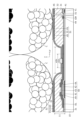


Classifications
-
- G—PHYSICS
- G02—OPTICS
- G02F—OPTICAL DEVICES OR ARRANGEMENTS FOR THE CONTROL OF LIGHT BY MODIFICATION OF THE OPTICAL PROPERTIES OF THE MEDIA OF THE ELEMENTS INVOLVED THEREIN; NON-LINEAR OPTICS; FREQUENCY-CHANGING OF LIGHT; OPTICAL LOGIC ELEMENTS; OPTICAL ANALOGUE/DIGITAL CONVERTERS
- G02F1/00—Devices or arrangements for the control of the intensity, colour, phase, polarisation or direction of light arriving from an independent light source, e.g. switching, gating or modulating; Non-linear optics
- G02F1/01—Devices or arrangements for the control of the intensity, colour, phase, polarisation or direction of light arriving from an independent light source, e.g. switching, gating or modulating; Non-linear optics for the control of the intensity, phase, polarisation or colour
- G02F1/13—Devices or arrangements for the control of the intensity, colour, phase, polarisation or direction of light arriving from an independent light source, e.g. switching, gating or modulating; Non-linear optics for the control of the intensity, phase, polarisation or colour based on liquid crystals, e.g. single liquid crystal display cells
- G02F1/133—Constructional arrangements; Operation of liquid crystal cells; Circuit arrangements
- G02F1/1333—Constructional arrangements; Manufacturing methods
-
- G—PHYSICS
- G02—OPTICS
- G02F—OPTICAL DEVICES OR ARRANGEMENTS FOR THE CONTROL OF LIGHT BY MODIFICATION OF THE OPTICAL PROPERTIES OF THE MEDIA OF THE ELEMENTS INVOLVED THEREIN; NON-LINEAR OPTICS; FREQUENCY-CHANGING OF LIGHT; OPTICAL LOGIC ELEMENTS; OPTICAL ANALOGUE/DIGITAL CONVERTERS
- G02F1/00—Devices or arrangements for the control of the intensity, colour, phase, polarisation or direction of light arriving from an independent light source, e.g. switching, gating or modulating; Non-linear optics
- G02F1/01—Devices or arrangements for the control of the intensity, colour, phase, polarisation or direction of light arriving from an independent light source, e.g. switching, gating or modulating; Non-linear optics for the control of the intensity, phase, polarisation or colour
- G02F1/165—Devices or arrangements for the control of the intensity, colour, phase, polarisation or direction of light arriving from an independent light source, e.g. switching, gating or modulating; Non-linear optics for the control of the intensity, phase, polarisation or colour based on translational movement of particles in a fluid under the influence of an applied field
- G02F1/1675—Constructional details
-
- G—PHYSICS
- G06—COMPUTING OR CALCULATING; COUNTING
- G06F—ELECTRIC DIGITAL DATA PROCESSING
- G06F3/00—Input arrangements for transferring data to be processed into a form capable of being handled by the computer; Output arrangements for transferring data from processing unit to output unit, e.g. interface arrangements
- G06F3/01—Input arrangements or combined input and output arrangements for interaction between user and computer
- G06F3/03—Arrangements for converting the position or the displacement of a member into a coded form
- G06F3/041—Digitisers, e.g. for touch screens or touch pads, characterised by the transducing means
-
- G—PHYSICS
- G06—COMPUTING OR CALCULATING; COUNTING
- G06F—ELECTRIC DIGITAL DATA PROCESSING
- G06F3/00—Input arrangements for transferring data to be processed into a form capable of being handled by the computer; Output arrangements for transferring data from processing unit to output unit, e.g. interface arrangements
- G06F3/01—Input arrangements or combined input and output arrangements for interaction between user and computer
- G06F3/03—Arrangements for converting the position or the displacement of a member into a coded form
- G06F3/041—Digitisers, e.g. for touch screens or touch pads, characterised by the transducing means
- G06F3/0416—Control or interface arrangements specially adapted for digitisers
- G06F3/04164—Connections between sensors and controllers, e.g. routing lines between electrodes and connection pads
-
- G—PHYSICS
- G06—COMPUTING OR CALCULATING; COUNTING
- G06F—ELECTRIC DIGITAL DATA PROCESSING
- G06F3/00—Input arrangements for transferring data to be processed into a form capable of being handled by the computer; Output arrangements for transferring data from processing unit to output unit, e.g. interface arrangements
- G06F3/01—Input arrangements or combined input and output arrangements for interaction between user and computer
- G06F3/03—Arrangements for converting the position or the displacement of a member into a coded form
- G06F3/041—Digitisers, e.g. for touch screens or touch pads, characterised by the transducing means
- G06F3/046—Digitisers, e.g. for touch screens or touch pads, characterised by the transducing means by electromagnetic means
-
- H—ELECTRICITY
- H10—SEMICONDUCTOR DEVICES; ELECTRIC SOLID-STATE DEVICES NOT OTHERWISE PROVIDED FOR
- H10D—INORGANIC ELECTRIC SEMICONDUCTOR DEVICES
- H10D86/00—Integrated devices formed in or on insulating or conducting substrates, e.g. formed in silicon-on-insulator [SOI] substrates or on stainless steel or glass substrates
- H10D86/40—Integrated devices formed in or on insulating or conducting substrates, e.g. formed in silicon-on-insulator [SOI] substrates or on stainless steel or glass substrates characterised by multiple TFTs
- H10D86/441—Interconnections, e.g. scanning lines
-
- G—PHYSICS
- G02—OPTICS
- G02F—OPTICAL DEVICES OR ARRANGEMENTS FOR THE CONTROL OF LIGHT BY MODIFICATION OF THE OPTICAL PROPERTIES OF THE MEDIA OF THE ELEMENTS INVOLVED THEREIN; NON-LINEAR OPTICS; FREQUENCY-CHANGING OF LIGHT; OPTICAL LOGIC ELEMENTS; OPTICAL ANALOGUE/DIGITAL CONVERTERS
- G02F1/00—Devices or arrangements for the control of the intensity, colour, phase, polarisation or direction of light arriving from an independent light source, e.g. switching, gating or modulating; Non-linear optics
- G02F1/01—Devices or arrangements for the control of the intensity, colour, phase, polarisation or direction of light arriving from an independent light source, e.g. switching, gating or modulating; Non-linear optics for the control of the intensity, phase, polarisation or colour
- G02F1/13—Devices or arrangements for the control of the intensity, colour, phase, polarisation or direction of light arriving from an independent light source, e.g. switching, gating or modulating; Non-linear optics for the control of the intensity, phase, polarisation or colour based on liquid crystals, e.g. single liquid crystal display cells
- G02F1/133—Constructional arrangements; Operation of liquid crystal cells; Circuit arrangements
- G02F1/1333—Constructional arrangements; Manufacturing methods
- G02F1/13338—Input devices, e.g. touch panels
-
- G—PHYSICS
- G02—OPTICS
- G02F—OPTICAL DEVICES OR ARRANGEMENTS FOR THE CONTROL OF LIGHT BY MODIFICATION OF THE OPTICAL PROPERTIES OF THE MEDIA OF THE ELEMENTS INVOLVED THEREIN; NON-LINEAR OPTICS; FREQUENCY-CHANGING OF LIGHT; OPTICAL LOGIC ELEMENTS; OPTICAL ANALOGUE/DIGITAL CONVERTERS
- G02F1/00—Devices or arrangements for the control of the intensity, colour, phase, polarisation or direction of light arriving from an independent light source, e.g. switching, gating or modulating; Non-linear optics
- G02F1/01—Devices or arrangements for the control of the intensity, colour, phase, polarisation or direction of light arriving from an independent light source, e.g. switching, gating or modulating; Non-linear optics for the control of the intensity, phase, polarisation or colour
- G02F1/165—Devices or arrangements for the control of the intensity, colour, phase, polarisation or direction of light arriving from an independent light source, e.g. switching, gating or modulating; Non-linear optics for the control of the intensity, phase, polarisation or colour based on translational movement of particles in a fluid under the influence of an applied field
- G02F1/166—Devices or arrangements for the control of the intensity, colour, phase, polarisation or direction of light arriving from an independent light source, e.g. switching, gating or modulating; Non-linear optics for the control of the intensity, phase, polarisation or colour based on translational movement of particles in a fluid under the influence of an applied field characterised by the electro-optical or magneto-optical effect
- G02F1/167—Devices or arrangements for the control of the intensity, colour, phase, polarisation or direction of light arriving from an independent light source, e.g. switching, gating or modulating; Non-linear optics for the control of the intensity, phase, polarisation or colour based on translational movement of particles in a fluid under the influence of an applied field characterised by the electro-optical or magneto-optical effect by electrophoresis
-
- G—PHYSICS
- G06—COMPUTING OR CALCULATING; COUNTING
- G06F—ELECTRIC DIGITAL DATA PROCESSING
- G06F2203/00—Indexing scheme relating to G06F3/00 - G06F3/048
- G06F2203/041—Indexing scheme relating to G06F3/041 - G06F3/045
- G06F2203/04102—Flexible digitiser, i.e. constructional details for allowing the whole digitising part of a device to be flexed or rolled like a sheet of paper
-
- G—PHYSICS
- G06—COMPUTING OR CALCULATING; COUNTING
- G06F—ELECTRIC DIGITAL DATA PROCESSING
- G06F3/00—Input arrangements for transferring data to be processed into a form capable of being handled by the computer; Output arrangements for transferring data from processing unit to output unit, e.g. interface arrangements
- G06F3/01—Input arrangements or combined input and output arrangements for interaction between user and computer
- G06F3/03—Arrangements for converting the position or the displacement of a member into a coded form
- G06F3/041—Digitisers, e.g. for touch screens or touch pads, characterised by the transducing means
- G06F3/0412—Digitisers structurally integrated in a display
Definitions
- the present invention relates to a reflective display, and in particular to a reflective display that supports electromagnetic induction (EMR) pen input.
- EMR electromagnetic induction
- Electronic paper is a type of reflective display that uses external light to display images.
- Patent documents 1 and 2 and non-patent document 1 disclose an example of the structure of electronic paper. As shown in these documents, electronic paper has a structure in which a light-reflecting layer containing reflective elements such as microcapsules is sandwiched between a pixel electrode and a common electrode. The pixel electrode is disposed on the upper surface of a backplane that also contains pixel transistors, gate lines, data lines, etc.
- the inventors of this application are considering making the reflective display compatible with electromagnetic induction (EMR) pen input.
- EMR electromagnetic induction
- one of the objectives of the present invention is to provide a reflective display that is compatible with electromagnetic induction (EMR) pen input while achieving a low profile.
- EMR electromagnetic induction
- a reflective display includes a cover layer including an operation surface on which a position indicator having an inductor is operated, a reflective display layer including a plurality of reflective elements each of which reflects light incident from the cover layer at a set gradation, a backplane provided at a position farther from the reflective display layer as viewed from the operation surface, and a common electrode layer including a common electrode provided between the cover layer and the reflective display layer, the backplane having, within a display area overlapping with the plurality of reflective elements in a planar view, a plurality of pixel electrodes arranged in a matrix along a first direction and a second direction intersecting the first direction, a plurality of data lines each extending along the first direction, and a plurality of first electromagnetic induction sensor electrodes each extending along the first direction, the plurality of first electromagnetic induction sensor electrodes being used to detect the position of the position indicator within the operation surface by generating an electromagnetic induction effect between the inductor.
- a reflective display includes a cover layer including an operation surface on which a position indicator having an inductor is operated, a reflective display layer including a plurality of reflective elements each of which reflects light incident from the cover layer at a set gradation, a backplane provided at a position farther from the reflective display layer as viewed from the operation surface, and a common electrode provided between the cover layer and the reflective display layer, the backplane having, within a display area overlapping with the plurality of reflective elements in a planar view, a plurality of pixel electrodes arranged in a matrix along a first direction and a second direction intersecting the first direction, a plurality of gate lines each extending along the second direction, and a plurality of second electromagnetic induction sensor electrodes each extending along the second direction, the plurality of second electromagnetic induction sensor electrodes being used to detect the position of the position indicator within the operation surface by generating an electromagnetic induction effect between the inductor and the plurality of second electromagnetic induction sensor electrodes.
- a reflective display includes a cover layer including an operation surface on which a position indicator having an inductor is operated, a reflective display layer including a plurality of reflective elements that each reflect light incident from the cover layer at a set gradation, a backplane provided at a position farther from the reflective display layer as viewed from the operation surface, and a common electrode provided between the cover layer and the reflective display layer, the backplane having, within a display area overlapping with the plurality of reflective elements in a planar view, a plurality of pixel electrodes arranged in a matrix along a first direction and a second direction intersecting the first direction, and a plurality of linear conductors each extending along the first direction, the plurality of linear conductors being used as either a plurality of data lines used to supply data signals to the pixel electrodes by time division, or a plurality of first electromagnetic induction sensor electrodes used to detect the position of the position indicator within the operation surface by generating an electromagnetic induction effect between the inductor.
- At least one of a plurality of first electromagnetic induction sensor electrodes and a plurality of second electromagnetic induction sensor electrodes is provided within the backplane, making it possible to realize a low-profile reflective display that supports electromagnetic induction (EMR) pen input.
- EMR electromagnetic induction
- FIG. 1 is a diagram showing a configuration of a computer 1 according to a first embodiment of the present invention.
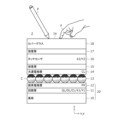
- FIG. 2 is a diagram showing a layer structure of a reflective display 2.
- FIG. 2 is a circuit diagram of the reflective display 2.
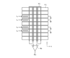
- FIG. 2 is a diagram showing the positional relationship of various wirings included in the reflective display 2.
- 11 is a diagram for explaining a process performed by the sensor controller 4 to detect the position of the pen P using the sensor electrodes X1 and Y1.
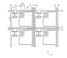
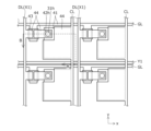
- FIG. 4 is a diagram showing a schematic planar structure of a portion of a circuit layer 11 corresponding to the circuit diagram of FIG. 3 .
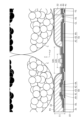
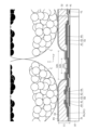
- FIG. 7 is a schematic cross-sectional view of the backplane 20 corresponding to the line AA shown in FIG. 6.
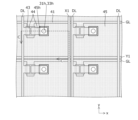
- FIG. 4 is a diagram showing a schematic planar structure of a portion of a circuit layer 11 included in a computer 1 according to a second embodiment of the present invention, the portion corresponding to the circuit diagram of FIG. 3 .
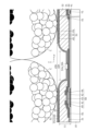
- 9 is a schematic cross-sectional view of the backplane 20 corresponding to the line BB shown in FIG. 8.
- FIG. 11 is a diagram showing the positional relationship of various wirings included in a reflective display 2 according to a second embodiment of the present invention.
- 10 is a diagram showing a schematic planar structure of a portion of a circuit layer 11 included in a computer 1 according to a third embodiment of the present invention, the portion corresponding to the circuit diagram of FIG. 3 .
- FIG. 12 is a schematic cross-sectional view of the backplane 20 corresponding to the line CC shown in FIG. 11.
- FIG. 13 is a diagram showing the positional relationship of various wirings included in a reflective display 2 according to a fourth embodiment of the present invention.
- 10 is a diagram showing a schematic planar structure of a portion of a circuit layer 11 included in a computer 1 according to a fourth embodiment of the present invention, the portion corresponding to the circuit diagram of FIG. 3 .
- 15 is a schematic cross-sectional view of the backplane 20 corresponding to the line DD shown in FIG. 14.
- FIG. 13 is a diagram showing the positional relationship of various wirings included in a reflective display 2 according to a fifth embodiment of the present invention.
- 13A and 13B are diagrams illustrating a process performed by a sensor controller 4 according to a fifth embodiment of the present invention to detect the position of a pen P using sensor electrodes X1 and Y1.
- 13A and 13B are diagrams illustrating a process performed by a sensor controller 4 according to a first modified example of the fifth embodiment of the present invention.
- 13A and 13B are diagrams illustrating a process performed by a sensor controller 4 according to a second modified example of the fifth embodiment of the present invention.
- 13 is a diagram showing an example of the layer structure of the reflective display 2 in which the sensor electrodes X1 and Y1 are arranged in a layer other than the circuit layer 11.
- FIG. 13 is a diagram showing an example of the layer structure of the reflective display 2 in which the sensor electrodes X1 and Y1 are arranged in a layer other than the circuit layer 11.
- FIG. 13 is a diagram showing the layer structure of the reflective display 2 when both sensor electrodes X1 and Y1 are used to receive a reception signal Rx.
- FIG. 1 is a diagram showing the configuration of a computer 1 according to a first embodiment of the present invention.
- the computer 1 according to this embodiment is configured to include a reflective display 2, a host processor 3, and a sensor controller 4.
- FIG. 2 is a diagram showing the layer structure of the reflective display 2.
- the reflective display 2 is composed of a substrate 10, a circuit layer 11, a pixel electrode layer 12, a reflective display layer 13, a common electrode layer 14, an adhesive layer 15, a touch sensor 16, an adhesive layer 17, and a cover glass 18 (cover layer).
- the substrate 10, the circuit layer 11, and the pixel electrode layer 12 form the backplane 20 of the reflective display 2.
- the surface of the cover glass 18 is the display surface of the reflective display 2, and also forms the operation surface 1a for input by a pen P (position indicator) (pen input) and input by a finger F (touch input).
- FIG. 1 shows only a part of the layer structure shown in FIG. 2.
- the circuit layer 11 is provided with a plurality of gate lines GL, a plurality of data lines DL, a plurality of common potential lines CL, and a plurality of sensor electrodes X1, Y1.
- the pixel electrode layer 12 is provided with a plurality of pixel electrodes PX
- the common electrode layer 14 is provided with one or more common potential lines CL (common electrodes)
- the touch sensor 16 is provided with sensor electrodes X2, Y2.
- Each of the multiple sensor electrodes X1, Y1 is an electromagnetic induction sensor electrode used for detecting the position of the pen P by the electromagnetic induction (EMR) method, and plays a role in generating an electromagnetic induction effect between the inductor that constitutes a resonant circuit provided in the pen P.
- the sensor electrodes X2, Y2 are electric field sensor electrodes used for detecting the position of the finger F by the capacitance method.
- a predetermined common potential (e.g., ground potential) is supplied from the host processor 3 to the common potential lines CL in the circuit layer 11 and the common potential lines CL including the common potential line CL in the common electrode layer 14.
- the common potential lines CL in the common electrode layer 14 and the sensor electrodes X2, Y2 are made of a transparent conductive film such as indium tin oxide (ITO) so as not to interfere with the display of the reflective display 2.
- ITO indium tin oxide
- the pixel electrodes PX included in the pixel electrode layer 12 are arranged in a matrix along the x direction and y direction (direction intersecting the x direction).
- the reflective display layer 13 has a plurality of reflective elements C arranged therein.
- Each reflective element C is an element that reflects light incident from the cover glass 18 with a gradation set by the potential of the nearest pixel electrode PX.
- the reflective display 2 is an electrophoretic electronic paper, and in this case the reflective elements C are formed of spherical microcapsules as shown in the figure.
- the reflective display 2 can also be formed by electronic powder electronic paper or a reflective liquid crystal display.
- the reflective display 2 is an electrophoretic electronic paper
- oil, a number of white pigment elements, and a number of black pigment elements are enclosed within the reflective element C.
- These white pigment elements and black pigment elements are pre-charged positively and negatively, respectively, and are configured to be able to migrate within the oil.
- a potential is applied to a pixel electrode PX
- an amount of white pigment elements or black pigment elements according to the potential migrates toward the operation surface 1a within the reflective element C near that pixel electrode PX.
- a black and white display is realized with a gradation (set gradation) according to the potential applied to the pixel electrode PX.
- a color display is also possible by using a color filter.
- the rectangular area A1 represents the display area of the reflective display 2 (the area overlapping with the multiple reflective elements C in the reflective display layer 13 in a plan view). Outside the display area A1 is the bezel area A2. As shown in FIG. 1, multiple wirings SL and a terminal area TA including multiple terminals are arranged in the bezel area A2. Among these, the multiple wirings SL are provided to connect wirings and electrodes arranged in the circuit layer 11, the common electrode layer 14, and the touch sensor 16 to terminals in the terminal area TA. In order to avoid cluttering the drawing, FIG. 1 shows only a schematic diagram of a portion of the multiple wirings SL actually provided in the reflective display 2. Each terminal in the terminal area TA is connected to the host processor 3 or the sensor controller 4 via wiring provided outside the reflective display 2.
- FIG. 3 is a circuit diagram of the reflective display 2.
- FIG. 4 is a diagram showing the positional relationship of various wirings included in the reflective display 2.
- FIG. 3 shows a circuit for four pixel electrodes PX, but in reality, many more pixel electrodes PX are provided.
- FIG. 4 shows 12 gate lines GL, data lines DL, common potential lines CL, eight sensor electrodes X1, and six sensor electrodes Y1, but in reality, many more wirings are provided. This also applies to FIG. 10, FIG. 13, and FIG. 16 to FIG. 19 shown later.
- the gate lines GL and the sensor electrodes Y1 are each extended along the x direction as shown in FIG. 4. As shown in FIG. 3, the gate lines GL are provided for each row of pixel electrodes PX, and the sensor electrodes Y1 are provided at a ratio of one for every several rows of pixel electrodes PX. Thus, the number of gate lines GL and the number of rows of pixel electrodes PX match, while the number of sensor electrodes Y1 is smaller than the number of rows of pixel electrodes PX. More specifically, it is preferable to set the pitch of the gate lines GL to several hundred ⁇ m and the pitch of the sensor electrodes Y1 to several mm.
- the data lines DL, common potential lines CL, and sensor electrodes X1 are each extended along the y direction as shown in FIG. 4.
- the data lines DL and common potential lines CL are each provided for each column of pixel electrodes PX, and the sensor electrodes X1 are provided at a ratio of one for every several columns of pixel electrodes PX. Therefore, the number of data lines DL and common potential lines CL matches the number of columns of pixel electrodes PX, while the number of sensor electrodes X1 is smaller than the number of columns of pixel electrodes PX. More specifically, it is preferable that the pitch of each of the data lines DL and common potential lines CL is several hundred ⁇ m, and the pitch of the sensor electrodes X1 is several mm.
- the multiple sensor electrodes X1 are connected to each other two at a time from one end in the x direction by a base electrode BE connected to the end farthest from the terminal area TA (see FIG. 1).
- the base electrodes BE are disposed within the bezel area A2 in a plan view. This connection is made in order to form a loop coil using the two sensor electrodes X1 for receiving an alternating magnetic field sent from an inductor in the pen P.
- the end of each sensor electrode X1 close to the terminal area TA is connected to the sensor controller 4 via wiring SL.
- each sensor electrode Y1 are connected to the sensor controller 4 via wiring SL.
- each gate line GL is alternately connected to the host processor 3 via wiring SL at one end or the other end.
- each data line DL and each common potential line CL is connected to the host processor 3 via wiring SL at the end closest to the terminal area TA.
- FIG. 5 is a diagram explaining the process performed by the sensor controller 4 to detect the position of the pen P using the sensor electrodes X1, Y1.
- the sensor controller 4 is configured to select the multiple sensor electrodes Y1 one by one in sequence, excluding two sensor electrodes Y1 from each end in the y direction, and each time select the multiple loop coils one by one in sequence, excluding one loop coil each from each end in the x direction (loop coils formed by two sensor electrodes X1; the same applies below).
- the sensor controller 4 is configured to supply an AC current iA to one end of each of two sensor electrodes Y1 adjacent to one side of the selected sensor electrode Y1, and an AC current iB to one end of each of two sensor electrodes Y1 adjacent to the other side.
- the AC current iA is a current that oscillates at a constant frequency and phase
- the AC current iB is a current obtained by inverting the phase of the AC current iA .
- the AC currents iA and iB are sinusoidal signals as shown in the figure, but they may also be rectangular wave signals.
- the sensor controller 4 also connects the other end of each of the four sensor electrodes Y1 that supply the AC currents iA and iB to a ground terminal. Instead of connecting to the ground terminal, the other ends of the sensor electrodes Y1 may be connected to each other.
- a change in magnetic flux occurs above the selected sensor electrode Y1.
- the inductor of the pen P enters the changing magnetic flux (alternating magnetic field)
- an electromagnetic induction effect occurs between the sensor electrode Y1 and the inductor, and a change in current occurs in the inductor.
- an alternating magnetic field is emitted from the pen P, and an electromotive force is generated in the sensor electrode X1 located nearby.
- the sensor controller 4 has a differential amplifier 4a, and is configured to connect a selected loop coil and the loop coils on both sides of the selected loop coil in series between two input terminals of the differential amplifier 4a.
- a current is generated in the corresponding loop coil and is supplied to the sensor controller 4 via the differential amplifier 4a.
- the sensor controller 4 obtains the current thus supplied from the differential amplifier 4a as a reception signal Rx from the pen P corresponding to each loop coil, immediately after supplying the AC currents iA and iB to the sensor electrode Y1 for a predetermined time.
- the sensor controller 4 acquires the reception signal Rx at each loop coil for each sensor electrode Y1.
- the sensor controller 4 derives the distribution of the signal strength of the acquired multiple reception signals Rx on the operation surface 1a, and derives the position of the pen P based on the result.
- the above-mentioned base electrode BE is disposed on one or the other end of the sensor electrode Y1 to use each sensor electrode Y1 as a loop coil, while one end of each sensor electrode X1 (the end farther from the terminal area TA) may be connected in advance to a ground terminal or may be connected to each other.
- the reflective display 2 is configured to have a pixel transistor 50 and a storage capacitor 51 for each pixel electrode PX.
- the control electrode of the pixel transistor 50 is connected to the corresponding gate line GL, one controlled electrode is connected to the corresponding data line DL, and the other controlled electrode is connected to the corresponding pixel electrode PX.
- one electrode of the storage capacitor 51 is connected to the corresponding pixel electrode PX, and the other electrode is connected to the corresponding common potential line CL.
- FIG. 6 is a diagram showing a schematic planar structure of a portion of the circuit layer 11 corresponding to the circuit diagram of FIG. 3, and FIG. 7 is a schematic cross-sectional view of the backplane 20 corresponding to the line A-A shown in FIG. 6.
- FIG. 6 and FIG. 7 are schematic diagrams for understanding the structure, and therefore the configurations shown in each diagram do not necessarily match.
- a portion of the reflective element C in the reflective display layer 13 is also shown to facilitate understanding of the structure.
- the circuit layer 11 is composed of a gate conductor film 41, a gate insulating film 42, a semiconductor film 43, a source/drain conductor film 44, a passivation film 31, and an overcoat film 32.
- the gate conductor film 41 is a metal film formed on the upper surface of the substrate 10, and constitutes the gate line GL, the control electrode of the pixel transistor 50, one electrode of the storage capacitor 51, and the sensor electrode Y1.
- the portion of the gate conductor film 41 that constitutes the sensor electrode Y1 extends along the gate line GL.
- the gate insulating film 42 is an insulating film formed to cover the upper surface of the gate conductor film 41, and constitutes the gate insulating film of the pixel transistor 50 and a dielectric disposed between the electrodes of the storage capacitor 51.
- the gate insulating film 42 is also configured to have a contact hole 42h on the upper side of a portion that is an extension of a portion of the gate conductor film 41 that constitutes one electrode of the storage capacitor 51.
- the semiconductor film 43 is an amorphous silicon film formed on the upper surface of the gate insulating film 42 at a position that overlaps with the control electrode of the pixel transistor 50 in a plan view, and constitutes the channel layer of the pixel transistor 50.
- the source drain conductor film 44 is a metal film formed on the upper surface of the gate insulating film 42 and the semiconductor film 43, and constitutes the data line DL, the common potential line CL, the other electrode of the storage capacitor 51, and the sensor electrode X1, as well as one and the other controlled electrodes of the pixel transistor 50.
- the portion of the source drain conductor film 44 that constitutes the sensor electrode X1 extends between the data line DL and the storage capacitor 51 adjacent in the x direction.
- the source drain conductor film 44 also serves as an internal wiring that connects the other controlled electrode of the pixel transistor 50 to one electrode of the storage capacitor 51 and the pixel electrode PX.
- the source drain conductor film 44 is connected to the gate conductor film 41 as one electrode of the storage capacitor 51 via the contact hole 42h described above.
- the passivation film 31 is an insulating film for protecting the pixel transistor 50 and the storage capacitor 51 from dust and moisture, and is formed on the upper side of the source-drain conductor film 44 so as to cover the entire surface.
- a contact hole 31h having a smaller diameter than the contact hole 42h is provided in the center of the contact hole 42h.
- the overcoat film 32 is also a protective insulating film, and is formed on the upper side of the passivation film 31 so as to cover the entire surface.
- a contact hole 32h having a larger diameter than the contact hole 42h is provided at the same position as the contact hole 31h. Note that while the diameter of each reflective element C is approximately 25 ⁇ m, the diameter of the contact hole 32h is usually 10 ⁇ m or less.
- the pixel electrodes PX are made of a conductive film formed on the upper surface of the overcoat film 32. Unlike the common potential line CL in the common electrode layer 14, the pixel electrodes PX do not need to be transparent, but are usually made of indium tin oxide (ITO), the same as the common potential line CL in the common electrode layer 14. This is to prevent the pixel electrodes PX from oxidizing during the manufacturing process of the reflective display 2. In other words, the backplane 20 and each layer (front plane) above the reflective display layer 13 are usually made in separate processes, and then the two planes are bonded together. At this time, the pixel electrodes PX are temporarily exposed to air, and if the pixel electrodes PX were made of a metal film such as aluminum, they would oxidize immediately. By forming the pixel electrodes PX using indium tin oxide (ITO), it is possible to avoid such oxidation.
- ITO indium tin oxide
- the multiple sensor electrodes X1, Y1 used to detect the position of the pen P by the electromagnetic induction (EMR) method are provided within the backplane 20 of the reflective display 2, making it possible to realize a low-profile reflective display 2 that is compatible with pen input by the electromagnetic induction (EMR) method.
- the computer 1 according to this embodiment differs from the computer 1 according to the first embodiment in that, rather than providing a sensor electrode X1 in addition to the data line DL, the data line DL is also used as the sensor electrode X1.
- the computer 1 according to this embodiment is similar to the computer 1 according to the first embodiment, so the following description will focus on the differences from the computer 1 according to the first embodiment.
- FIG. 8 is a diagram showing the planar structure of a portion of the circuit layer 11 included in the computer 1 according to this embodiment that corresponds to the circuit diagram of FIG. 3, and FIG. 9 is a schematic cross-sectional view of the backplane 20 that corresponds to the line B-B shown in FIG. 8.
- the circuit layer 11 according to this embodiment differs from the circuit layer 11 according to the first embodiment in that it does not have the portion of the source-drain conductor film 44 that constitutes the sensor electrode X1.
- FIG. 10 is a diagram showing the positional relationship of various wirings included in the reflective display 2 according to this embodiment.
- the reflective display 2 according to this embodiment is configured with switch groups 60 and 61, each of which is made up of a plurality of switch elements.
- the switch group 60 is a switch group consisting of multiple switch elements provided for each data line DL.
- Each switch element is provided midway along the wiring SL, and is composed of a single-pole, double-throw switch having a common terminal connected to the end of the corresponding data line DL on the terminal area TA side, one selection terminal connected to the host processor 3, and the other selection terminal connected to the sensor controller 4.
- the switch group 61 is a switch group consisting of a plurality of switch elements provided for each pair of adjacent data lines DL.
- Each switch element is provided midway on the base electrode BE connected to the end of each data line DL farther from the terminal area TA, and is composed of a single-pole, single-throw switch having one terminal connected to one of the corresponding two data lines DL and the other terminal connected to the other of the corresponding two data lines DL.
- the sensor controller 4 also uses the linear conductors constituting the data lines DL as the sensor electrodes X1 by time division. Specifically, the sensor controller 4 first sets each switch element constituting the switch group 60 to the host processor 3 side at the timing when the host processor 3 drives the data lines DL, and turns off each switch element constituting the switch group 61. This allows the host processor 3 to drive the data lines DL as usual. On the other hand, the sensor controller 4 sets each switch element constituting the switch group 60 to the sensor controller 4 side at the timing when the host processor 3 does not drive the data lines DL (blank period), and turns on each switch element constituting the switch group 61. This forms a loop coil by the linear conductors constituting the data lines DL, so that the sensor controller 4 can obtain the received signal Rx from the pen P via the sensor electrode X1, as in the first embodiment.
- the computer 1 also provides the multiple sensor electrodes X1, Y1 used to detect the position of the pen P by the electromagnetic induction (EMR) method within the backplane 20 of the reflective display 2, making it possible to realize a low-profile reflective display 2 that is compatible with pen input by the electromagnetic induction (EMR) method.
- EMR electromagnetic induction
- the linear conductors that make up the data lines DL are also used as the sensor electrodes X1, making it possible to reduce the number of wiring lines in the display area A1.
- the computer 1 according to this embodiment differs from the computer 1 according to the first embodiment in terms of the structure of the storage capacitor 51.
- the computer 1 according to this embodiment is similar to the computer 1 according to the first embodiment, so the following description will focus on the differences from the computer 1 according to the first embodiment.
- FIG. 11 is a diagram showing a schematic planar structure of a portion of the circuit layer 11 included in the computer 1 according to this embodiment, which corresponds to the circuit diagram of FIG. 3, and FIG. 12 is a schematic cross-sectional view of the backplane 20 corresponding to the line C-C shown in FIG. 11.
- the circuit layer 11 according to this embodiment differs from the circuit layer 11 according to the first embodiment in that the electrode of the storage capacitor 51 is composed of the pixel electrode PX and a conductive film 45 formed on the upper surface of the overcoat film 32.
- the gate conductor film 41 and the source/drain conductor film 44 according to this embodiment do not have any portion that constitutes the electrodes of the storage capacitor 51.
- a conductive film 45 is formed on the upper surface of the overcoat film 32, and a second passivation film 33 is further formed on the upper surface of the conductive film 45.
- the pixel electrode PX is formed on the upper surface of the passivation film 33.
- the storage capacitor 51 according to this embodiment is configured with the conductive film 45 thus formed as the other electrode and the pixel electrode PX as one electrode.
- the passivation film 33 serves as a dielectric disposed between the electrodes of the storage capacitor 51.
- a predetermined common potential e.g., ground potential
- the conductive film 45 is configured to have a contact hole 45h with a larger diameter than the contact hole 32h of the overcoat film 32 at the same position as the contact hole 32h.
- the passivation film 33 is configured to have a contact hole 33h with approximately the same diameter as the contact hole 31h at the same position as the contact hole 31h of the passivation film 31.
- the pixel electrode PX according to this embodiment is connected to the source-drain conductor film 44 that constitutes the other controlled electrode of the pixel transistor 50 via the contact holes 31h and 46h.
- the computer 1 is similar to the first embodiment in that the multiple sensor electrodes X1, Y1 used to detect the position of the pen P by the electromagnetic induction (EMR) method are provided within the backplane 20 of the reflective display 2, so that it is possible to realize a low-profile reflective display 2 that is compatible with pen input by the electromagnetic induction (EMR) method, similar to the first embodiment.
- EMR electromagnetic induction
- the computer 1 according to this embodiment differs from the computer 1 according to the third embodiment in that the connection between each gate line GL and the host processor 3 is realized via a gate wiring GW that extends within the display area A1.
- the computer 1 according to this embodiment is similar to the computer 1 according to the third embodiment, so the following description will focus on the differences from the computer 1 according to the third embodiment.
- FIG. 13 is a diagram showing the positional relationship of various wirings included in the reflective display 2 according to this embodiment.
- FIG. 14 is a diagram showing a schematic planar structure of a portion of the circuit layer 11 included in the computer 1 according to this embodiment, which corresponds to the circuit diagram in FIG. 3, and
- FIG. 15 is a schematic cross-sectional view of the backplane 20 corresponding to the line D-D shown in FIG. 14.
- the circuit layer 11 is configured to have a gate wiring GW and a gate via conductor GV for each gate line GL.
- the gate via conductor GV is a via conductor provided to penetrate the gate insulating film 42, and serves to connect the corresponding gate wiring GW and gate line GL to each other.
- the gate wiring GW is a wiring that extends in the y direction from the position of the gate via conductor GV toward the terminal area TA side, and is connected to the host processor 3 at the end on the terminal area TA side via wiring SL.
- the computer 1 is similar to the third embodiment in that the multiple sensor electrodes X1, Y1 used to detect the position of the pen P by electromagnetic induction (EMR) are provided within the backplane 20 of the reflective display 2, so that, like the third embodiment, it is possible to realize a low-profile reflective display 2 that is compatible with pen input by electromagnetic induction (EMR).
- EMR electromagnetic induction
- the wiring SL in the bezel area A2 in the horizontal direction as viewed from the terminal area TA can be reduced, making it possible to narrow the bezel area A2.
- the computer 1 according to this embodiment differs from the computer 1 according to the first embodiment in the way in which the sensor electrodes X1, Y1 for detecting the position of the pen P are used.
- the computer 1 according to this embodiment is similar to the computer 1 according to the first embodiment, so the following description will focus on the differences from the computer 1 according to the first embodiment.
- FIG. 16 is a diagram showing the positional relationship of various wirings included in the reflective display 2 according to this embodiment. However, in this figure, the gate lines GL, data lines DL, and common potential lines CL are omitted. As shown in this figure, the reflective display 2 according to this embodiment is configured with switch groups 62 to 64, each of which is made up of a plurality of switch elements.
- the switch group 62 is a switch group consisting of multiple switch elements that connect two adjacent sensor electrodes Y1 with one sensor electrode Y1 between them. Each switch element is provided midway through the base electrode BE that is connected to one end of each sensor electrode Y1, and is composed of a single-pole, single-throw switch having one terminal connected to one of the corresponding two sensor electrodes Y1 and the other terminal connected to the other of the corresponding two sensor electrodes Y1.
- the switch group 63 is a switch group consisting of multiple switch elements that connect two adjacent sensor electrodes Y1 from among the multiple sensor electrodes Y1 that are not connected to the switch group 62.
- Each switch element is provided midway through the base electrode BE that is connected to the other end of each sensor electrode Y1, and is composed of a single-pole, single-throw switch having one terminal connected to one of the corresponding two sensor electrodes Y1 and the other terminal connected to the other of the corresponding two sensor electrodes Y1.
- the switch group 64 is a switch group consisting of multiple switch elements that connect two adjacent sensor electrodes X1 to each other. Each switch element is provided midway through the base electrode BE that is connected to the end of each sensor electrode X1 that is farther from the terminal area TA, and is composed of a single-pole, single-throw switch that has one terminal connected to one of the corresponding two sensor electrodes X1 and the other terminal connected to the other of the corresponding two sensor electrodes X1.
- FIG. 17(a) and (b) are diagrams for explaining the process performed by the sensor controller 4 according to this embodiment to detect the position of the pen P using the sensor electrodes X1 and Y1.
- the sensor controller 4 When starting the position detection process, the sensor controller 4 according to this embodiment first turns on all of the switch elements constituting the switch groups 62 and 64 as shown in FIG. 17(a). Then, every other switch element constituting the switch group 64 is turned on, and of the sensor electrodes Y1, excluding one each at both ends in the y direction, the one at the end in the y direction is selected. By turning on every other switch element constituting the switch group 64, multiple loop coils are formed.
- the sensor controller 4 has a differential amplifier 4a shown in FIG. 5 for each loop coil thus formed, and both ends of the formed loop coil are connected to the two input terminals of the corresponding differential amplifier 4a.
- the sensor controller 4 supplies an AC current iA to one end of one sensor electrode Y1 adjacent to one side of the selected sensor electrode Y1, and an AC current iB to one end of each sensor electrode Y1 adjacent to the other side.
- the specific contents of the AC currents iA and iB are as described in the first embodiment.
- This causes a change in the magnetic flux above the selected sensor electrode Y1.
- the inductor of the pen P enters the changing magnetic flux (alternating magnetic field)
- an electromagnetic induction action occurs between the sensor electrode Y1 and the inductor, and a change in current occurs in the inductor.
- an alternating magnetic field is sent from the pen P, and an electromotive force is generated in the sensor electrode X1 located nearby.
- the electromotive force thus generated generates a current in each loop coil, which is supplied to the sensor controller 4 via the differential amplifier 4a.
- the sensor controller 4 obtains the current thus supplied from the differential amplifier 4a as a reception signal Rx from the pen P corresponding to each loop coil, immediately after supplying the AC currents iA and iB to the sensor electrode Y1 for a predetermined time.
- the sensor controller 4 switches on and off the multiple switch elements that make up the switch group 64, and connects both ends of the newly formed loop coil to each of the two input terminals of the differential amplifier 4a that correspond to each of them. Then, by performing the same process as above, the reception signal Rx from the pen P that corresponds to each loop coil is obtained.
- the sensor controller 4 repeatedly executes the above process while shifting the selected sensor electrode Y1 one by one.
- the sensor controller 4 acquires the reception signal Rx at each loop coil for each sensor electrode Y1.
- the sensor controller 4 derives the distribution of the signal strength of the acquired multiple reception signals Rx on the operation surface 1a, and derives the position of the pen P based on the result.
- the computer 1 is similar to the first embodiment in that the multiple sensor electrodes X1, Y1 used to detect the position of the pen P by the electromagnetic induction (EMR) method are provided within the backplane 20 of the reflective display 2, so that it is possible to realize a low-profile reflective display 2 that is compatible with pen input by the electromagnetic induction (EMR) method, similar to the first embodiment.
- EMR electromagnetic induction
- the computer 1 can simultaneously acquire reception signals Rx from pens P corresponding to multiple loop coils, making it possible to frequently derive the position of the pen P.
- FIGS. 18(a) and 18(b) are diagrams for explaining the processing performed by the sensor controller 4 according to the first modified example of this embodiment.
- the sensor controller 4 according to this modified example differs from the sensor controller 4 according to this embodiment in that it supplies an AC current iA to one end of each of the two sensor electrodes Y1 adjacent to one side of the selected sensor electrode Y1 , and an AC current iB to one end of each of the two sensor electrodes Y1 adjacent to the other side.
- the method of supplying these AC currents iA and iB is the same as that described in the first embodiment. This makes it possible to increase the transmission strength of the alternating magnetic field generated above the sensor electrode Y1.
- FIGS. 19(a) and 19(b) are diagrams explaining the processing performed by a sensor controller 4 according to a second modified example of this embodiment.
- the sensor controller 4 according to this modified example differs from the sensor controller 4 according to this embodiment in that it transmits an alternating magnetic field from the sensor electrode X1 and receives the alternating magnetic field transmitted by the pen P at the sensor electrode Y1.
- the sensor controller 4 when starting the position detection process, the sensor controller 4 according to this embodiment first turns on all of the switch elements constituting the switch group 64, as shown in FIG. 19(a). Then, in each of the switch groups 62 and 64, every other switch element included therein is turned on, and of the multiple sensor electrodes X1 excluding the two sensor electrodes X1 at each end in the x direction, the one at the extreme end in the x direction is selected. By turning on every other switch element included in each of the switch groups 62 and 64, multiple loop coils are formed.
- the sensor controller 4 has a differential amplifier 4a shown in FIG. 5 for each of the loop coils thus formed, and both ends of the formed loop coil are connected to the two input terminals of the corresponding differential amplifier 4a.
- the sensor controller 4 supplies an AC current iA to one end of two sensor electrodes X1 adjacent to one side of the selected sensor electrode X1, and an AC current iB to one end of each of two sensor electrodes X1 adjacent to the other side.
- This causes a change in magnetic flux above the selected sensor electrode X1.
- the inductor of the pen P enters the changing magnetic flux (alternating magnetic field)
- electromagnetic induction occurs between the sensor electrode X1 and the inductor, causing a change in current in the inductor.
- an alternating magnetic field is sent from the pen P, and an electromotive force is generated in the sensor electrode Y1 located nearby.
- the electromotive force thus generated generates a current in each loop coil, which is supplied to the sensor controller 4 via the differential amplifier 4a.
- the sensor controller 4 obtains the current thus supplied from the differential amplifier 4a as a reception signal Rx from the pen P corresponding to each loop coil, immediately after supplying the AC currents iA and iB to the sensor electrode X1 for a predetermined time.
- the sensor controller 4 switches on and off the multiple switch elements that make up the switch groups 62 and 64, and connects both ends of the newly formed loop coil to the two corresponding input terminals of the differential amplifier 4a. Then, by performing the same process as above, the reception signal Rx from the pen P corresponding to each loop coil is obtained.
- the sensor controller 4 repeatedly executes the above process while shifting the selected sensor electrode X1 one by one.
- the sensor controller 4 acquires the reception signal Rx of each loop coil for each sensor electrode X1.
- the sensor controller 4 derives the distribution of the signal strength of the acquired multiple reception signals Rx on the operation surface 1a, and derives the position of the pen P based on the result.
- the present modified example also makes it possible to derive the position of the pen P, similarly to the sensor controller 4 according to the present embodiment.
- the sensor controller 4 according to the present modified example may be configured to supply an AC current iA to one end of each sensor electrode Y1 adjacent to one side of the selected sensor electrode Y1, and an AC current iB to one end of each sensor electrode Y1 adjacent to the other side, similarly to the sensor controller 4 according to the present embodiment.
- the sensor electrodes X1, Y1 are arranged in the circuit layer 11, but by arranging the sensor electrodes X1, Y1 in another layer, it is possible to realize a low-profile reflective display 2 that supports electromagnetic induction (EMR) pen input, just like in each of the above embodiments. Specific examples are described below.
- EMR electromagnetic induction
- Figures 20 and 21 are diagrams showing examples of the layer structure of the reflective display 2 when the sensor electrodes X1 and Y1 are arranged on a layer other than the circuit layer 11.
- the example shown in FIG. 20 is an example in which a sensor electrode X1 is provided in the common electrode layer 14.
- the sensor electrode X1 may be provided separately from the common potential line CL in the common electrode layer 14, or the common potential line CL may be used as the sensor electrode X1 by time division.
- a sensor electrode Y1 may be provided in the common electrode layer 14 instead of the sensor electrode X1.
- the sensor electrode Y1 may be provided separately from the common potential line CL in the common electrode layer 14, or the common potential line CL may be used as the sensor electrode Y1 by time division.
- the example shown in FIG. 20 is an example in which a sensor electrode X1 is provided in the touch sensor 16.
- the sensor electrode X1 may be provided separately from the sensor electrode X2, or the sensor electrode X2 may be used as the sensor electrode X1 by time division.
- a sensor electrode Y1 may be provided in the touch sensor 16. In this case, too, the sensor electrode Y1 may be provided separately from the sensor electrode Y2, or the sensor electrode Y2 may be used as the sensor electrode Y1 by time division.
- one of the sensor electrodes X1, Y1 is used to transmit an alternating magnetic field and the other is used to receive the reception signal Rx, but it is also possible to use both of them to receive the reception signal Rx.
- FIG. 22 is a diagram showing the layer structure of the reflective display 2 when both sensor electrodes X1, Y1 are used to receive the reception signal Rx.
- a battery 70 is provided inside the pen P, and the pen P uses power supplied from this battery 70 to emit an alternating magnetic field from an inductor.
- the sensor controller 4 forms loop coils using each of the sensor electrodes X1, Y1, and derives the position of the pen P by receiving the alternating magnetic field emitted by the pen P in each loop coil.
Landscapes
- Engineering & Computer Science (AREA)
- Physics & Mathematics (AREA)
- Theoretical Computer Science (AREA)
- General Engineering & Computer Science (AREA)
- General Physics & Mathematics (AREA)
- Human Computer Interaction (AREA)
- Nonlinear Science (AREA)
- Electromagnetism (AREA)
- Optics & Photonics (AREA)
- Computer Networks & Wireless Communication (AREA)
- Mathematical Physics (AREA)
- Chemical & Material Sciences (AREA)
- Crystallography & Structural Chemistry (AREA)
- Position Input By Displaying (AREA)
Abstract
【課題】電磁誘導(EMR)方式のペン入力に対応する反射型ディスプレイの低背化を実現する。 【解決手段】本発明による反射型ディスプレイは、カバーグラス18から入射した光を設定階調でそれぞれ反射する複数の反射素子Cを含む反射表示層13と、操作面1aから見て反射表示層13より遠い位置に設けられたバックプレーン20と、カバーグラス18と反射表示層13の間に設けられた共通電極層14と、を含む。バックプレーン20は、表示領域内に、x方向及びy方向に沿ってマトリクス状に配置された複数の画素電極PXと、それぞれy方向に沿って延設された複数のデータ線DLと、それぞれy方向に沿って延設された複数のセンサ電極X1と、を有する。複数のセンサ電極X1は、ペンP内のインダクタとの間で電磁誘導作用を生じさせることによって操作面1a内におけるペンPの位置を検出するために用いられるものである。
Description
本発明は反射型ディスプレイに関し、特に、電磁誘導(EMR)方式のペン入力に対応する反射型ディスプレイに関する。
電子ペーパーは、外光を利用して画像を表示する反射型ディスプレイの一種である。特許文献1,2及び非特許文献1には、電子ペーパーの構造の一例が開示されている。これらの文献に示されるように、電子ペーパーは、マイクロカプセルなどの反射素子を含む光反射層が画素電極と共通電極の間に挟まれた構造を有している。画素電極は、画素トランジスタ、ゲート線、データ線などを含むバックプレーンの上面に配置される。
S. E. Burns外21名,「A scalable manufacturing process for flexible active-matrix e-paper displays」,Journal of the Society for Information Display,2005年7月
ところで、本願の発明者は、反射型ディスプレイを電磁誘導(EMR)方式のペン入力に対応させることを検討している。しかしながら、そのためには反射型ディスプレイのバックプレーンの下側(表示面から遠い側)に位置検出用のセンサを配置する必要があり、全体の厚みが大きくなってしまうため、改善が必要となっていた。
したがって、本発明の目的の一つは、電磁誘導(EMR)方式のペン入力に対応しつつも低背化を実現できる反射型ディスプレイを提供することにある。
本発明の一側面による反射型ディスプレイは、インダクタを備えた位置指示器が操作される操作面を含むカバー層と、前記カバー層から入射した光を設定階調でそれぞれ反射する複数の反射素子を含む反射表示層と、前記操作面から見て前記反射表示層より遠い位置に設けられたバックプレーンと、前記カバー層と前記反射表示層の間に設けられた共通電極を含む共通電極層と、を含み、前記バックプレーンは、平面視で前記複数の反射素子と重なる表示領域内に、第1の方向及び該第1の方向と交差する第2の方向に沿ってマトリクス状に配置された複数の画素電極と、それぞれ前記第1の方向に沿って延設された複数のデータ線と、それぞれ前記第1の方向に沿って延設された複数の第1の電磁誘導センサ電極と、を有し、前記複数の第1の電磁誘導センサ電極は、前記インダクタとの間で電磁誘導作用を生じさせることによって前記操作面内における前記位置指示器の位置を検出するために用いられるものである、反射型ディスプレイである。
本発明の他の一側面による反射型ディスプレイは、インダクタを備えた位置指示器が操作される操作面を含むカバー層と、前記カバー層から入射した光を設定階調でそれぞれ反射する複数の反射素子を含む反射表示層と、前記操作面から見て前記反射表示層より遠い位置に設けられたバックプレーンと、前記カバー層と前記反射表示層の間に設けられた共通電極と、を含み、前記バックプレーンは、平面視で前記複数の反射素子と重なる表示領域内に、第1の方向及び該第1の方向と交差する第2の方向に沿ってマトリクス状に配置された複数の画素電極と、それぞれ前記第2の方向に沿って延設された複数のゲート線と、それぞれ前記第2の方向に沿って延設された複数の第2の電磁誘導センサ電極と、を有し、前記複数の第2の電磁誘導センサ電極は、前記インダクタとの間で電磁誘導作用を生じさせることによって前記操作面内における前記位置指示器の位置を検出するために用いられるものである、反射型ディスプレイである。
本発明のさらに他の一側面による反射型ディスプレイは、インダクタを備えた位置指示器が操作される操作面を含むカバー層と、前記カバー層から入射した光を設定階調でそれぞれ反射する複数の反射素子を含む反射表示層と、前記操作面から見て前記反射表示層より遠い位置に設けられたバックプレーンと、前記カバー層と前記反射表示層の間に設けられた共通電極と、を含み、前記バックプレーンは、平面視で前記複数の反射素子と重なる表示領域内に、第1の方向及び該第1の方向と交差する第2の方向に沿ってマトリクス状に配置された複数の画素電極と、それぞれ前記第1の方向に沿って延設された複数の線状導体とを有し、前記複数の線状導体は、時分割により、前記画素電極にデータ信号を供給するために用いられる複数のデータ線、及び、前記インダクタとの間で電磁誘導作用を生じさせることによって前記操作面内における前記位置指示器の位置を検出するために用いられる複数の第1の電磁誘導センサ電極のいずれか一方として用いられる、反射型ディスプレイである。
本発明によれば、複数の第1の電磁誘導センサ電極及び複数の第2の電磁誘導センサ電極の少なくとも一方をバックプレーン内に設けているので、電磁誘導(EMR)方式のペン入力に対応する反射型ディスプレイの低背化を実現することが可能になる。
以下、添付図面を参照しながら、本発明の実施の形態について詳細に説明する。
図1は、本発明の第1の実施の形態によるコンピュータ1の構成を示す図である。同図に示すように、本実施の形態によるコンピュータ1は、反射型ディスプレイ2と、ホストプロセッサ3と、センサコントローラ4とを有して構成される。
図2は、反射型ディスプレイ2の層構造を示す図である。同図に示すように、反射型ディスプレイ2は、基板10、回路層11、画素電極層12、反射表示層13、共通電極層14、接着層15、タッチセンサ16、接着層17、カバーグラス18(カバー層)を有して構成される。このうち基板10、回路層11、及び画素電極層12は、反射型ディスプレイ2のバックプレーン20を構成する。また、カバーグラス18の表面は、反射型ディスプレイ2の表示面であるとともに、ペンP(位置指示器)による入力(ペン入力)及び指Fによる入力(タッチ入力)の操作面1aを構成する。なお、図1には、図2に示した層構造の一部のみを図示している。
後ほど詳しく説明するが、回路層11には、複数のゲート線GL、複数のデータ線DL、複数の共通電位線CL、各複数のセンサ電極X1,Y1が設けられる。また、画素電極層12には複数の画素電極PXが設けられ、共通電極層14には1以上の共通電位線CL(共通電極)が設けられ、タッチセンサ16にはセンサ電極X2,Y2が設けられる。
各複数のセンサ電極X1,Y1は、電磁誘導(EMR)方式によるペンPの位置検出のために用いられる電磁誘導センサ電極であり、ペンP内に設けられる共振回路を構成するインダクタとの間で電磁誘導作用を生じさせる役割を果たす。また、センサ電極X2,Y2は、静電容量方式による指Fの位置検出のために用いられる電界センサ電極である。回路層11内の共通電位線CL、及び、共通電極層14内の共通電位線CLを含む共通電位線CLには、ホストプロセッサ3から所定の共通電位(例えば接地電位)が供給される。共通電極層14内の共通電位線CL、及び、センサ電極X2,Y2は、反射型ディスプレイ2の表示を妨げないよう、酸化インジウムスズ(ITO)などの透明導電膜によって構成される。
画素電極層12に含まれる複数の画素電極PXは、x方向及びy方向(x方向と交差する方向)に沿って、マトリクス状に配置される。反射表示層13には、複数の反射素子Cが配置される。各反射素子Cは、最も近くにある画素電極PXの電位によって設定される階調で、カバーグラス18から入射した光を反射する素子である。一例では、反射型ディスプレイ2は電気泳動方式の電子ペーパーであり、この場合の反射素子Cは、図示したような球状のマイクロカプセルによって構成される。電子粉流体方式の電子ペーパーや反射型の液晶ディスプレイにより反射型ディスプレイ2を構成することも可能である。
反射型ディスプレイ2が電気泳動方式の電子ペーパーである場合、反射素子Cの中には、オイルと、複数の白色顔料素子と、複数の黒色顔料素子とが封入される。これら白色顔料素子及び黒色顔料素子はそれぞれプラスとマイナスに予め帯電しており、オイル内を泳動可能に構成される。ある画素電極PXに電位を与えると、その画素電極PXの近傍にある反射素子C内において、電位に応じた量の白色顔料素子又は黒色顔料素子が操作面1a側に泳動する。この泳動の結果として、画素電極PXに与えた電位に従う階調(設定階調)での白黒表示が実現される。図示していないが、カラーフィルタを用いれば、カラー表示を行うことも可能である。
図1に戻り、矩形で示した領域A1は、反射型ディスプレイ2の表示領域(反射表示層13内の複数の反射素子Cと平面視で重なる領域)を表している。表示領域A1の外側はベゼル領域A2である。図1に示すように、ベゼル領域A2内には、複数の配線SLと、複数の端子を含む端子領域TAとが配置される。このうち複数の配線SLは、回路層11、共通電極層14、及びタッチセンサ16内に配置される配線や電極などを端子領域TA内の端子に接続するために設けられるものである。なお、図面が煩雑になることを避けるため、図1には、反射型ディスプレイ2に実際に設けられる複数の配線SLのうちの一部のみを模式的に図示している。端子領域TA内の各端子は、反射型ディスプレイ2外に設けられる配線を介して、ホストプロセッサ3又はセンサコントローラ4に接続される。
図3は、反射型ディスプレイ2の回路図である。また、図4は、反射型ディスプレイ2に含まれる各種配線の位置関係を示す図である。図3には4つの画素電極PX分の回路を示しているが、実際には、より多くの画素電極PXが設けられる。また、図4には、各12本のゲート線GL、データ線DL、共通電位線CL、8本のセンサ電極X1、6本のセンサ電極Y1を示しているが、実際には、より多くの配線が設けられる。この点は、後掲する図10,図13、図16~図19においても同様である。
ゲート線GL及びセンサ電極Y1はそれぞれ、図4に示すように、x方向に沿って延設される。図3に示すように、ゲート線GLは画素電極PXの行ごとに設けられ、センサ電極Y1は画素電極PXの複数行ごとに1本の割合で設けられる。したがって、ゲート線GLの本数と画素電極PXの行数とが一致する一方、センサ電極Y1の本数は画素電極PXの行数よりも小さくなる。より具体的には、ゲート線GLのピッチを数百μmとし、センサ電極Y1のピッチを数mmとすることが好適である。
またデータ線DL、共通電位線CL、及びセンサ電極X1はそれぞれ、図4に示すように、y方向に沿って延設される。図3に示すように、データ線DL及び共通電位線CLはそれぞれ画素電極PXの列ごとに設けられ、センサ電極X1は画素電極PXの複数列ごとに1本の割合で設けられる。したがって、データ線DL及び共通電位線CLそれぞれの本数と画素電極PXの列数とが一致する一方、センサ電極X1の本数は画素電極PXの列数よりも小さくなる。より具体的には、データ線DL及び共通電位線CLそれぞれのピッチを数百μmとし、センサ電極X1のピッチを数mmとすることが好適である。
図4に示すように、複数のセンサ電極X1は、端子領域TA(図1を参照)から遠い側の端部に接続された基部電極BEにより、x方向の一端側から2本ずつ、互いに接続される。基部電極BEは、平面視でベゼル領域A2内に配置される。この接続を行っているのは、2本のセンサ電極X1を用いて、ペンP内のインダクタから送出される交番磁界を受信するためのループコイルを形成するためである。各センサ電極X1の端子領域TAに近い側の端部は、配線SLを介してセンサコントローラ4に接続される。
一方、各センサ電極Y1は、両端で、配線SLを介してセンサコントローラ4に接続される。これに対し、各ゲート線GLは、y方向に見て交互に、一端及び他端のいずれか一方で、配線SLを介してホストプロセッサ3に接続される。また、各データ線DL及び各共通電位線CLはそれぞれ、端子領域TAに近い側の端部で、配線SLを介してホストプロセッサ3に接続される。
図5は、センサ電極X1,Y1を用いてペンPの位置を検出するためにセンサコントローラ4が行う処理を説明する図である。この処理においてセンサコントローラ4は、y方向の両端から2本ずつのセンサ電極Y1を除く複数のセンサ電極Y1を1本ずつ順に選択し、その都度、x方向の両端から1本ずつのループコイル(2本のセンサ電極X1によって形成されるループコイル。以下、同じ。)を除く複数のループコイルを1本ずつ順に選択するよう構成される。
図5に示すように、センサコントローラ4は、選択したセンサ電極Y1の一方側に隣接する2本のセンサ電極Y1それぞれの一端に交流電流iAを、他方側に隣接する2本のセンサ電極Y1それぞれの一端に交流電流iBを、それぞれ供給するよう構成される。交流電流iAは一定の周波数及び位相で振動する電流であり、交流電流iBは、交流電流iAの位相を反転させてなる電流である。典型的な交流電流iA,iBは、図示するような正弦波信号であるが、矩形波信号であってもよい。また、センサコントローラ4は、交流電流iA,iBを供給する4本のセンサ電極Y1それぞれの他端を接地端に接続する。なお、接地端に接続することに代え、各センサ電極Y1それぞれの他端を相互に接続することとしてもよい。センサコントローラ4がこのような動作を行うことにより、選択したセンサ電極Y1の上方に磁束の変化が生ずる。そして、変化する磁束(交番磁界)の中にペンPのインダクタが入ると、センサ電極Y1とインダクタとの間で電磁誘導作用が生じ、インダクタに電流の変化が発生する。その結果、ペンPから交番磁界が送出され、近傍に位置するセンサ電極X1に起電力が生ずる。
センサコントローラ4は差動アンプ4aを有しており、選択したループコイルとその両隣のループコイルをこの差動アンプ4aの2つの入力端子の間に直列に接続するよう構成される。ペンPが送出した交番磁界によってセンサ電極X1に起電力が発生すると、対応するループコイルに電流が発生し、差動アンプ4aを介してセンサコントローラ4に供給される。センサコントローラ4は、所定時間にわたってセンサ電極Y1に交流電流iA,iBを供給した直後にこうして差動アンプ4aから供給される電流を、各ループコイルに対応するペンPからの受信信号Rxとして取得する。
以上の処理により、センサコントローラ4は、センサ電極Y1ごとに、各ループコイルでの受信信号Rxを取得することになる。センサコントローラ4は、取得した複数の受信信号Rxの信号強度の操作面1a内における分布を導出し、その結果に基づいてペンPの位置を導出する。
なお、図5では、センサ電極Y1に交流電流iA,iBを供給し、センサ電極X1で受信信号Rxを受信する例を説明したが、センサ電極X1に交流電流iA,iBを供給し、センサ電極Y1で受信信号Rxを受信することとしてもよい。この場合、上述した基部電極BEをセンサ電極Y1の一端側又は他端側に配置することにより各センサ電極Y1をループコイルとして用いる一方、各センサ電極X1の一端(端子領域TAから遠い側の端部)を予め接地端に接続しておくか、或いは相互に接続しておけばよい。
図3に戻り、反射型ディスプレイ2の表示動作について、説明する。図3に示すように、反射型ディスプレイ2は、画素電極PXごとに画素トランジスタ50及びストレージキャパシタ51を有して構成される。画素トランジスタ50の制御電極は対応するゲート線GLに接続され、一方の被制御電極は対応するデータ線DLに接続され、他方の被制御電極は対応する画素電極PXに接続される。また、ストレージキャパシタ51の一方の電極は対応する画素電極PXに接続され、他方の電極は対応する共通電位線CLに接続される。これらの構成により、ホストプロセッサ3があるゲート線GLを活性化すると、そのゲート線GLに接続された一連の画素トランジスタ50がオンになり、対応する一連の画素電極PXが対応するデータ線DLに接続される。これによりホストプロセッサ3は、データ線DLの電位を制御することにより、各画素の設定階調を制御することが可能になる。また、画素トランジスタ50がオンになっている間、データ線DLの電位はストレージキャパシタ51にも与えられ、ストレージキャパシタ51を充電する。この充電によりストレージキャパシタ51に蓄積された電荷は画素トランジスタ50がオフになった後も維持されるので、各画素の表示状態は、対応するゲート線GLが非活性となっている間にも維持される。
図6は、回路層11のうち図3の回路図に対応する部分の平面構造を模式的に示す図であり、図7は、図6に示したA-A線に対応するバックプレーン20の模式的な断面図である。図6及び図7はいずれも構造を理解するための模式的な図であるので、各図に示す構成は必ずしも一致していない。図7には、構造の理解を容易にするために、反射表示層13内の反射素子Cについても一部を図示している。これらの点は、後掲する図8、図9、図11、図12、図14、図15についても同様である。以下、図6及び図7を参照しながら、バックプレーン20内の構造について詳細に説明する。
図6及び図7に示すように、回路層11は、ゲート導体膜41、ゲート絶縁膜42、半導体膜43、ソースドレイン導体膜44、パッシベーション膜31、オーバーコート膜32を有して構成される。
ゲート導体膜41は基板10の上面に形成された金属膜であり、ゲート線GL、画素トランジスタ50の制御電極、ストレージキャパシタ51の一方の電極、及びセンサ電極Y1を構成する。ゲート導体膜41のうちセンサ電極Y1を構成する部分は、ゲート線GLに沿って延設される。
ゲート絶縁膜42は、ゲート導体膜41の上面を覆うように形成された絶縁膜であり、画素トランジスタ50のゲート絶縁膜、及び、ストレージキャパシタ51の電極間に配置される誘電体を構成する。また、ゲート絶縁膜42は、ゲート導体膜41のうちストレージキャパシタ51の一方の電極を構成する部分を延長してなる部分の上側に、コンタクトホール42hを有して構成される。
半導体膜43は、ゲート絶縁膜42の上面のうち平面視で画素トランジスタ50の制御電極と重なる位置に形成されたアモルファスシリコン膜であり、画素トランジスタ50のチャネル層を構成する。
ソースドレイン導体膜44は、ゲート絶縁膜42及び半導体膜43の上面に形成された金属膜であり、データ線DL、共通電位線CL、ストレージキャパシタ51の他方の電極、及びセンサ電極X1を構成するとともに、画素トランジスタ50の一方及び他方の被制御電極を構成する。ソースドレイン導体膜44のうちセンサ電極X1を構成する部分は、x方向に隣接するデータ線DLとストレージキャパシタ51の間に延設される。また、ソースドレイン導体膜44は、画素トランジスタ50の他方の被制御電極をストレージキャパシタ51の一方の電極及び画素電極PXに接続する内部配線としての役割も果たす。ソースドレイン導体膜44は、上述したコンタクトホール42hを介して、ストレージキャパシタ51の一方の電極としてのゲート導体膜41に接続される。
パッシベーション膜31は、画素トランジスタ50及びストレージキャパシタ51をゴミや湿度から保護するための絶縁膜であり、ソースドレイン導体膜44の上側に、全面を覆うように形成される。パッシベーション膜31には、コンタクトホール42hの中央部分に、コンタクトホール42hよりも小径のコンタクトホール31hが設けられる。
オーバーコート膜32も保護用の絶縁膜であり、パッシベーション膜31の上側に、全面を覆うように形成される。オーバーコート膜32には、コンタクトホール31hと同じ位置に、コンタクトホール42hよりも大径のコンタクトホール32hが設けられる。なお、個々の反射素子Cの直径が25μm程度であるのに対し、コンタクトホール32hの直径は通常10μm以下となる。
画素電極PXは、オーバーコート膜32の上面に形成された導電膜によって構成される。画素電極PXは、共通電極層14内の共通電位線CLなどと異なり透明である必要はないが、通常、共通電極層14内の共通電位線CLと同じ酸化インジウムスズ(ITO)により形成される。これは、反射型ディスプレイ2の製造工程において画素電極PXが酸化してしまうことを防止するためである。すなわち、バックプレーン20と、反射表示層13より上側の各層(フロントプレーン)とは通常別工程でそれぞれ作られ、その後、両プレーンを貼り合わせることになるが、この際、画素電極PXが一時的に空気に曝露することになるため、もし画素電極PXがアルミニウムなどの金属膜により構成されていたとすると、すぐに酸化してしまうことになる。酸化インジウムスズ(ITO)を用いて画素電極PXを形成することにより、このような酸化を回避することが可能になる。
以上説明したように、本実施の形態によるコンピュータ1によれば、電磁誘導(EMR)方式によるペンPの位置検出のために用いられる各複数のセンサ電極X1,Y1を反射型ディスプレイ2のバックプレーン20内に設けているので、電磁誘導(EMR)方式のペン入力に対応する反射型ディスプレイ2の低背化を実現することが可能になる。
次に、本発明の第2の実施の形態によるコンピュータ1について、説明する。本実施の形態によるコンピュータ1は、データ線DLとは別にセンサ電極X1を設けるのではなく、データ線DLをセンサ電極X1としても用いる点で、第1の実施の形態によるコンピュータ1と相違する。その他の点では第1の実施の形態によるコンピュータ1と同様であるので、以下では、第1の実施の形態によるコンピュータ1との相違点に着目して説明を行う。
図8は、本実施の形態によるコンピュータ1に含まれる回路層11のうち図3の回路図に対応する部分の平面構造を示す図であり、図9は、図8に示したB-B線に対応するバックプレーン20の模式的な断面図である。図8及び図9に示すように、本実施の形態による回路層11は、ソースドレイン導体膜44のうちセンサ電極X1を構成する部分を有しない点で、第1の実施の形態による回路層11と相違する。
図10は、本実施の形態による反射型ディスプレイ2に含まれる各種配線の位置関係を示す図である。同図に示すように、本実施の形態による反射型ディスプレイ2は、それぞれ複数のスイッチ素子からなるスイッチ群60,61を有して構成される。
スイッチ群60は、データ線DLごとに設けられる複数のスイッチ素子からなるスイッチ群である。各スイッチ素子は配線SLの途中に設けられており、対応するデータ線DLの端子領域TA側の端部に接続された共通端子と、ホストプロセッサ3に接続された一方の選択端子と、センサコントローラ4に接続された他方の選択端子とを有する単極双投形のスイッチにより構成される。
スイッチ群61は、隣接する2本のデータ線DLごとに設けられる複数のスイッチ素子からなるスイッチ群である。各スイッチ素子は、各データ線DLの端子領域TAから遠い側の端部に接続された基部電極BEの途中に設けられており、対応する2本のデータ線DLの一方に接続された一方の端子と、対応する2本のデータ線DLの他方に接続された他方の端子とを有する単極単投形のスイッチにより構成される。
本実施の形態によるセンサコントローラ4は、データ線DLを構成する線状導体を、時分割により、センサ電極X1としても利用する。具体的に説明すると、センサコントローラ4は、まずホストプロセッサ3がデータ線DLを駆動するタイミングでは、スイッチ群60を構成する各スイッチ素子をホストプロセッサ3側にセットするとともに、スイッチ群61を構成する各スイッチ素子をオフにする。これにより、ホストプロセッサ3は通常どおり、データ線DLを駆動することができる。一方、センサコントローラ4は、ホストプロセッサ3がデータ線DLを駆動しないタイミング(ブランク期間)では、スイッチ群60を構成する各スイッチ素子をセンサコントローラ4側にセットするとともに、スイッチ群61を構成する各スイッチ素子をオンにする。これにより、データ線DLを構成する線状導体によりループコイルが形成されるので、センサコントローラ4は、第1の実施の形態と同様に、センサ電極X1を介してペンPからの受信信号Rxとして取得することが可能になる。
以上説明したように、本実施の形態によるコンピュータ1によっても、電磁誘導(EMR)方式によるペンPの位置検出のために用いられる各複数のセンサ電極X1,Y1を反射型ディスプレイ2のバックプレーン20内に設けているので、電磁誘導(EMR)方式のペン入力に対応する反射型ディスプレイ2の低背化を実現することが可能になる。
また、本実施の形態によるコンピュータ1によれば、データ線DLを構成する線状導体をセンサ電極X1としても利用するので、表示領域A1内の配線数を減らすことが可能になる。
次に、本発明の第3の実施の形態によるコンピュータ1について、説明する。本実施の形態によるコンピュータ1は、ストレージキャパシタ51の構造の点で第1の実施形態によるコンピュータ1と相違する。その他の点では第1の実施の形態によるコンピュータ1と同様であるので、以下では、第1の実施の形態によるコンピュータ1との相違点に着目して説明を行う。
図11は、本実施の形態によるコンピュータ1に含まれる回路層11のうち図3の回路図に対応する部分の平面構造を模式的に示す図であり、図12は、図11に示したC-C線に対応するバックプレーン20の模式的な断面図である。図11及び図12に示すように、本実施の形態による回路層11は、ストレージキャパシタ51の電極が画素電極PXと、オーバーコート膜32の上面に形成された導電膜45とによって構成される点で、第1の実施の形態による回路層11と相違する。
図7と図12を比較すると理解されるように、本実施の形態によるゲート導体膜41及びソースドレイン導体膜44は、ストレージキャパシタ51の電極を構成する部分を有しない。一方、本実施の形態においては、オーバーコート膜32の上面に導電膜45が形成され、さらにその上面に2つ目のパッシベーション膜33が形成される。画素電極PXは、パッシベーション膜33の上面に形成される。そして、本実施の形態によるストレージキャパシタ51は、こうして形成された導電膜45を他方の電極とし、画素電極PXを一方の電極として構成される。パッシベーション膜33は、ストレージキャパシタ51の電極間に配置される誘電体としての役割を果たす。導電膜45には、第1の実施の形態で説明した共通電位線CLと同様、ホストプロセッサ3から所定の共通電位(例えば接地電位)が供給される。
導電膜45は、コンタクトホール32hと同じ位置に、オーバーコート膜32のコンタクトホール32hよりも大径のコンタクトホール45hを有して構成される。また、パッシベーション膜33は、パッシベーション膜31のコンタクトホール31hと同じ位置に、コンタクトホール31hと略同径のコンタクトホール33hを有して構成される。本実施の形態による画素電極PXは、コンタクトホール31h,46hを介して、画素トランジスタ50の他方の被制御電極を構成するソースドレイン導体膜44に接続される。
本実施の形態によるコンピュータ1によっても、電磁誘導(EMR)方式によるペンPの位置検出のために用いられる各複数のセンサ電極X1,Y1を反射型ディスプレイ2のバックプレーン20内に設けている点は第1の実施の形態と同様であるので、第1の実施の形態と同様に、電磁誘導(EMR)方式のペン入力に対応する反射型ディスプレイ2の低背化を実現することが可能になる。
次に、本発明の第4の実施の形態によるコンピュータ1について、説明する。本実施の形態によるコンピュータ1は、各ゲート線GLとホストプロセッサ3の接続が表示領域A1内に延設されるゲート配線GWを介して実現される点で、第3の実施形態によるコンピュータ1と相違する。その他の点では第3の実施の形態によるコンピュータ1と同様であるので、以下では、第3の実施の形態によるコンピュータ1との相違点に着目して説明を行う。
図13は、本実施の形態による反射型ディスプレイ2に含まれる各種配線の位置関係を示す図である。また、図14は、本実施の形態によるコンピュータ1に含まれる回路層11のうち図3の回路図に対応する部分の平面構造を模式的に示す図であり、図15は、図14に示したD-D線に対応するバックプレーン20の模式的な断面図である。
本実施の形態による回路層11は、ゲート線GLごとに、ゲート配線GW及びゲートビア導体GVを有して構成される。ゲートビア導体GVは、ゲート絶縁膜42を貫通して設けられるビア導体であり、対応するゲート配線GW及びゲート線GLを相互に接続する役割を果たす。ゲート配線GWは、ゲートビア導体GVの位置から端子領域TA側に向かい、y方向に沿って延設される配線であり、端子領域TA側の端部で、配線SLを介してホストプロセッサ3に接続される。
本実施の形態によるコンピュータ1によっても、電磁誘導(EMR)方式によるペンPの位置検出のために用いられる各複数のセンサ電極X1,Y1を反射型ディスプレイ2のバックプレーン20内に設けている点は第3の実施の形態と同様であるので、第3の実施の形態と同様に、電磁誘導(EMR)方式のペン入力に対応する反射型ディスプレイ2の低背化を実現することが可能になる。
また、本実施の形態によるコンピュータ1によれば、端子領域TAから見て横方向のベゼル領域A2内の配線SLを減らすことができるので、ベゼル領域A2を狭くすることが可能になる。
次に、本発明の第5の実施の形態によるコンピュータ1について、説明する。本実施の形態によるコンピュータ1は、ペンPの位置を検出するためのセンサ電極X1,Y1の使い方の点で、第1の実施の形態によるコンピュータ1と相違する。その他の点では第1の実施の形態によるコンピュータ1と同様であるので、以下では、第1の実施の形態によるコンピュータ1との相違点に着目して説明を行う。
図16は、本実施の形態による反射型ディスプレイ2に含まれる各種配線の位置関係を示す図である。ただし、同図においては、ゲート線GL、データ線DL、及び共通電位線CLの記載は省略している。同図に示すように、本実施の形態による反射型ディスプレイ2は、それぞれ複数のスイッチ素子からなるスイッチ群62~64を有して構成される。
スイッチ群62は、間に1本のセンサ電極Y1を挟んで隣接する2本のセンサ電極Y1を相互に接続する複数のスイッチ素子からなるスイッチ群である。各スイッチ素子は、各センサ電極Y1の一端に接続された基部電極BEの途中に設けられており、対応する2本のセンサ電極Y1の一方に接続された一方の端子と、対応する2本のセンサ電極Y1の他方に接続された他方の端子とを有する単極単投形のスイッチにより構成される。
スイッチ群63は、スイッチ群62に接続されていない複数のセンサ電極Y1の中で隣接する2本のセンサ電極Y1を相互に接続する複数のスイッチ素子からなるスイッチ群である。各スイッチ素子は、各センサ電極Y1の他端に接続された基部電極BEの途中に設けられており、対応する2本のセンサ電極Y1の一方に接続された一方の端子と、対応する2本のセンサ電極Y1の他方に接続された他方の端子とを有する単極単投形のスイッチにより構成される。
スイッチ群64は、隣接する2本のセンサ電極X1を相互に接続する複数のスイッチ素子からなるスイッチ群である。各スイッチ素子は、各センサ電極X1の端子領域TAから遠い側の端部に接続された基部電極BEの途中に設けられており、対応する2本のセンサ電極X1の一方に接続された一方の端子と、対応する2本のセンサ電極X1の他方に接続された他方の端子とを有する単極単投形のスイッチにより構成される。
図17(a)(b)は、センサ電極X1,Y1を用いて行うペンPの位置を検出するために、本実施の形態によるセンサコントローラ4が行う処理を説明する図である。本実施の形態によるセンサコントローラ4は、位置検出処理を開始するにあたり、まず初めに、図17(a)に示すように、スイッチ群62,64を構成する各スイッチ素子をすべてオンにする。そして、スイッチ群64を構成する複数のスイッチ素子を1つおきにオンとするとともに、y方向の両端から1本ずつのセンサ電極Y1を除く複数のセンサ電極Y1のうち、y方向の最も端にある1本を選択する。スイッチ群64を構成する複数のスイッチ素子を1つおきにオンすることで、複数のループコイルが形成されることになる。センサコントローラ4は、こうして形成されるループコイルごとに図5に示した差動アンプ4aを有しており、形成したループコイルの両端を、対応する差動アンプ4aの2つの入力端子のそれぞれに接続する。
続いてセンサコントローラ4は、選択したセンサ電極Y1の一方側に隣接する1本のセンサ電極Y1の一端に交流電流iAを、他方側に隣接する1本のセンサ電極Y1それぞれの一端に交流電流iBを、それぞれ供給する。交流電流iA,iBの具体的な内容は、第1の実施の形態で説明したとおりである。これにより、選択したセンサ電極Y1の上方に磁束の変化が生ずる。そして、変化する磁束(交番磁界)の中にペンPのインダクタが入ると、センサ電極Y1とインダクタとの間で電磁誘導作用が生じ、インダクタに電流の変化が発生する。その結果、ペンPから交番磁界が送出され、近傍に位置するセンサ電極X1に起電力が生ずる。こうして生じた起電力により各ループコイルに電流が発生し、差動アンプ4aを介してセンサコントローラ4に供給される。センサコントローラ4は、所定時間にわたってセンサ電極Y1に交流電流iA,iBを供給した直後にこうして差動アンプ4aから供給される電流を、各ループコイルに対応するペンPからの受信信号Rxとして取得する。
次にセンサコントローラ4は、図17(b)に示すように、スイッチ群64を構成する複数のスイッチ素子のオンオフを切り替え、新たに形成したループコイルの両端を、それぞれに対応する差動アンプ4aの2つの入力端子のそれぞれに接続する。そして、上記と同様の処理を行うことにより、各ループコイルに対応するペンPからの受信信号Rxを取得する。
センサコントローラ4は、以上の処理を、選択するセンサ電極Y1を1本ずつシフトしながら、繰り返し実行する。すべてのセンサ電極Y1の選択と、その後の処理が終了すると、センサコントローラ4は、センサ電極Y1ごとに、各ループコイルでの受信信号Rxを取得することになる。センサコントローラ4は、取得した複数の受信信号Rxの信号強度の操作面1a内における分布を導出し、その結果に基づいてペンPの位置を導出する。
本実施の形態によるコンピュータ1によっても、電磁誘導(EMR)方式によるペンPの位置検出のために用いられる各複数のセンサ電極X1,Y1を反射型ディスプレイ2のバックプレーン20内に設けている点は第1の実施の形態と同様であるので、第1の実施の形態と同様に、電磁誘導(EMR)方式のペン入力に対応する反射型ディスプレイ2の低背化を実現することが可能になる。
また、本実施の形態によるコンピュータ1によれば、複数のループコイルに対応するペンPからの受信信号Rxを一度に取得することができるので、ペンPの位置導出を高頻度に行うことが可能になる。
図18(a)(b)は、本実施の形態の第1の変形例によるセンサコントローラ4が行う処理を説明する図である。本変形例によるセンサコントローラ4は、選択したセンサ電極Y1の一方側に隣接する2本のセンサ電極Y1それぞれの一端に交流電流iAを、他方側に隣接する2本のセンサ電極Y1それぞれの一端に交流電流iBを、それぞれ供給する点で、本実施の形態によるセンサコントローラ4と相違する。この交流電流iA,iBの供給方法は、第1の実施の形態で説明したものと同様である。こうすることにより、センサ電極Y1の上方に発生する交番磁界の送出強度を高めることが可能になる。
図19(a)(b)は、本実施の形態の第2の変形例によるセンサコントローラ4が行う処理を説明する図である。本変形例によるセンサコントローラ4は、センサ電極X1から交番磁界を送出し、ペンPが送出した交番磁界をセンサ電極Y1で受信する点で、本実施の形態によるセンサコントローラ4と相違する。
具体的に説明すると、本実施の形態によるセンサコントローラ4は、位置検出処理を開始するにあたり、まず初めに、図19(a)に示すように、スイッチ群64を構成する各スイッチ素子をすべてオンにする。そして、スイッチ群62,64のそれぞれにおいて、その中に含まれる複数のスイッチ素子を1つおきにオンとするとともに、x方向の両端から2本ずつのセンサ電極X1を除く複数のセンサ電極X1のうち、x方向の最も端にある1本を選択する。スイッチ群62,64のそれぞれにおいて、その中に含まれる複数のスイッチ素子を1つおきにオンとすることで、複数のループコイルが形成されることになる。センサコントローラ4は、こうして形成されるループコイルごとに図5に示した差動アンプ4aを有しており、形成したループコイルの両端を、対応する差動アンプ4aの2つの入力端子のそれぞれに接続する。
続いてセンサコントローラ4は、選択したセンサ電極X1の一方側に隣接する2本のセンサ電極X1の一端に交流電流iAを、他方側に隣接する2本のセンサ電極X1それぞれの一端に交流電流iBを、それぞれ供給する。これにより、選択したセンサ電極X1の上方に磁束の変化が生ずる。そして、変化する磁束(交番磁界)の中にペンPのインダクタが入ると、センサ電極X1とインダクタとの間で電磁誘導作用が生じ、インダクタに電流の変化が発生する。その結果、ペンPから交番磁界が送出され、近傍に位置するセンサ電極Y1に起電力が生ずる。こうして生じた起電力により各ループコイルに電流が発生し、差動アンプ4aを介してセンサコントローラ4に供給される。センサコントローラ4は、所定時間にわたってセンサ電極X1に交流電流iA,iBを供給した直後にこうして差動アンプ4aから供給される電流を、各ループコイルに対応するペンPからの受信信号Rxとして取得する。
次にセンサコントローラ4は、図19(b)に示すように、スイッチ群62,64を構成する複数のスイッチ素子のオンオフを切り替え、新たに形成したループコイルの両端を、それぞれに対応する差動アンプ4aの2つの入力端子のそれぞれに接続する。そして、上記と同様の処理を行うことにより、各ループコイルに対応するペンPからの受信信号Rxを取得する。
センサコントローラ4は、以上の処理を、選択するセンサ電極X1を1本ずつシフトしながら、繰り返し実行する。すべてのセンサ電極X1の選択と、その後の処理が終了すると、センサコントローラ4は、センサ電極X1ごとに、各ループコイルでの受信信号Rxを取得することになる。センサコントローラ4は、取得した複数の受信信号Rxの信号強度の操作面1a内における分布を導出し、その結果に基づいてペンPの位置を導出する。このように、本変形例によっても、本実施の形態によるセンサコントローラ4と同様に、ペンPの位置を導出することが可能になる。なお、本変形例によるセンサコントローラ4を、本実施の形態によるセンサコントローラ4と同様に、選択したセンサ電極Y1の一方側に隣接する1本のセンサ電極Y1それぞれの一端に交流電流iAを、他方側に隣接する1本のセンサ電極Y1それぞれの一端に交流電流iBを供給するように構成してもよいのは勿論である。
以上、本発明の好ましい実施の形態について説明したが、本発明はこうした実施の形態に何等限定されるものではなく、本発明が、その要旨を逸脱しない範囲において、種々なる態様で実施され得ることは勿論である。
例えば、上記各実施の形態では、回路層11の中にセンサ電極X1,Y1を配置したが、他の層の中にセンサ電極X1,Y1を配置することによっても、上記各実施の形態と同様に、電磁誘導(EMR)方式のペン入力に対応する反射型ディスプレイ2の低背化を実現することができる。以下、具体的な例を挙げて説明する。
図20及び図21はそれぞれ、回路層11以外の層にセンサ電極X1,Y1を配置する場合における反射型ディスプレイ2の層構造の例を示す図である。
図20に示す例は、共通電極層14の中にセンサ電極X1を設ける例である。この場合、共通電極層14内の共通電位線CLとは別にセンサ電極X1を設けてもよいし、時分割により共通電位線CLをセンサ電極X1として用いることとしてもよい。また、センサ電極X1に代えてセンサ電極Y1を共通電極層14内に設けることとしてもよい。この場合においても、共通電極層14内の共通電位線CLとは別にセンサ電極Y1を設けてもよいし、時分割により共通電位線CLをセンサ電極Y1として用いることとしてもよい。
図20に示す例は、タッチセンサ16の中にセンサ電極X1を設ける例である。この場合、センサ電極X2とは別にセンサ電極X1を設けてもよいし、時分割によりセンサ電極X2をセンサ電極X1として用いることとしてもよい。また、センサ電極X1に代えてセンサ電極Y1をタッチセンサ16内に設けることとしてもよい。この場合においても、センサ電極Y2とは別にセンサ電極Y1を設けてもよいし、時分割によりセンサ電極Y2をセンサ電極Y1として用いることとしてもよい。
また、上記各実施の形態では、センサ電極X1,Y1の一方を交番磁界送出用として用い、他方を受信信号Rxの受信用として用いたが、両方を受信信号Rxの受信用として用いることも可能である。
図22は、センサ電極X1,Y1の両方を受信信号Rxの受信用として用いる場合における反射型ディスプレイ2の層構造を示す図である。同図に示すように、本変形例では、ペンPの中にバッテリー70が設けられており、ペンPは、このバッテリー70から供給される電力を用いて、インダクタから交番磁界を送出する。センサコントローラ4は、センサ電極X1,Y1のそれぞれによりループコイルを形成し、各ループコイルにおいて、ペンPが送出した交番磁界を受信することにより、ペンPの位置導出を行えばよい。
1 コンピュータ
1a 操作面
2 反射型ディスプレイ
3 ホストプロセッサ
4 センサコントローラ
4a 差動アンプ
10 基板
11 回路層
12 画素電極層
13 反射表示層
14 共通電極層
15,17 接着層
16 タッチセンサ
18 カバーグラス
20 バックプレーン
31,33 パッシベーション膜
31h,32h,33h,45h,46h コンタクトホール
32 オーバーコート膜
41 ゲート導体膜
42 ゲート絶縁膜
43 半導体膜
44 ソースドレイン導体膜
45 導電膜
50 画素トランジスタ
51 ストレージキャパシタ
60~64 スイッチ群
70 バッテリー
A1 表示領域
A2 ベゼル領域
BE 基部電極
C 反射素子
CL 共通電位線
DL データ線
F 指
GL ゲート線
GV ゲートビア導体
GW ゲート配線
P ペン
PX 画素電極
SL 配線
TA 端子領域
X1,Y1 電磁誘導センサ電極
X2,Y2 電界センサ電極
1a 操作面
2 反射型ディスプレイ
3 ホストプロセッサ
4 センサコントローラ
4a 差動アンプ
10 基板
11 回路層
12 画素電極層
13 反射表示層
14 共通電極層
15,17 接着層
16 タッチセンサ
18 カバーグラス
20 バックプレーン
31,33 パッシベーション膜
31h,32h,33h,45h,46h コンタクトホール
32 オーバーコート膜
41 ゲート導体膜
42 ゲート絶縁膜
43 半導体膜
44 ソースドレイン導体膜
45 導電膜
50 画素トランジスタ
51 ストレージキャパシタ
60~64 スイッチ群
70 バッテリー
A1 表示領域
A2 ベゼル領域
BE 基部電極
C 反射素子
CL 共通電位線
DL データ線
F 指
GL ゲート線
GV ゲートビア導体
GW ゲート配線
P ペン
PX 画素電極
SL 配線
TA 端子領域
X1,Y1 電磁誘導センサ電極
X2,Y2 電界センサ電極
Claims (19)
- インダクタを備えた位置指示器が操作される操作面を含むカバー層と、
前記カバー層から入射した光を設定階調でそれぞれ反射する複数の反射素子を含む反射表示層と、
前記操作面から見て前記反射表示層より遠い位置に設けられたバックプレーンと、
前記カバー層と前記反射表示層の間に設けられた共通電極を含む共通電極層と、を含み、
前記バックプレーンは、平面視で前記複数の反射素子と重なる表示領域内に、
第1の方向及び該第1の方向と交差する第2の方向に沿ってマトリクス状に配置された複数の画素電極と、
それぞれ前記第1の方向に沿って延設された複数のデータ線と、
それぞれ前記第1の方向に沿って延設された複数の第1の電磁誘導センサ電極と、を有し、
前記複数の第1の電磁誘導センサ電極は、前記インダクタとの間で電磁誘導作用を生じさせることによって前記操作面内における前記位置指示器の位置を検出するために用いられるものである、
反射型ディスプレイ。 - 前記バックプレーンは、前記表示領域内に、
それぞれ前記第2の方向に沿って延設された複数のゲート線と、
それぞれ前記第2の方向に沿って延設された複数の第2の電磁誘導センサ電極と、をさらに有し、
前記複数の第2の電磁誘導センサ電極は、前記インダクタとの間で電磁誘導作用を生じさせることによって前記操作面内における前記位置指示器の位置を検出するために用いられるものである、
請求項1に記載の反射型ディスプレイ。 - 前記共通電極層は、前記表示領域内に、それぞれ前記第2の方向に沿って延設された複数の第2の電磁誘導センサ電極をさらに有し、
前記複数の第2の電磁誘導センサ電極は、前記インダクタとの間で電磁誘導作用を生じさせることによって前記操作面内における前記位置指示器の位置を検出するために用いられるものである、
請求項1に記載の反射型ディスプレイ。 - 前記カバー層と前記共通電極層の間に設けられたタッチセンサをさらに含み、
前記タッチセンサは、前記表示領域内に、それぞれ前記第2の方向に沿って延設された複数の第2の電磁誘導センサ電極を有する、
請求項1に記載の反射型ディスプレイ。 - インダクタを備えた位置指示器が操作される操作面を含むカバー層と、
前記カバー層から入射した光を設定階調でそれぞれ反射する複数の反射素子を含む反射表示層と、
前記操作面から見て前記反射表示層より遠い位置に設けられたバックプレーンと、
前記カバー層と前記反射表示層の間に設けられた共通電極と、を含み、
前記バックプレーンは、平面視で前記複数の反射素子と重なる表示領域内に、
第1の方向及び該第1の方向と交差する第2の方向に沿ってマトリクス状に配置された複数の画素電極と、
それぞれ前記第2の方向に沿って延設された複数のゲート線と、
それぞれ前記第2の方向に沿って延設された複数の第2の電磁誘導センサ電極と、を有し、
前記複数の第2の電磁誘導センサ電極は、前記インダクタとの間で電磁誘導作用を生じさせることによって前記操作面内における前記位置指示器の位置を検出するために用いられるものである、
反射型ディスプレイ。 - インダクタを備えた位置指示器が操作される操作面を含むカバー層と、
前記カバー層から入射した光を設定階調でそれぞれ反射する複数の反射素子を含む反射表示層と、
前記操作面から見て前記反射表示層より遠い位置に設けられたバックプレーンと、
前記カバー層と前記反射表示層の間に設けられた共通電極と、を含み、
前記バックプレーンは、平面視で前記複数の反射素子と重なる表示領域内に、第1の方向及び該第1の方向と交差する第2の方向に沿ってマトリクス状に配置された複数の画素電極と、それぞれ前記第1の方向に沿って延設された複数の線状導体とを有し、
前記複数の線状導体は、時分割により、前記画素電極にデータ信号を供給するために用いられる複数のデータ線、及び、前記インダクタとの間で電磁誘導作用を生じさせることによって前記操作面内における前記位置指示器の位置を検出するために用いられる複数の第1の電磁誘導センサ電極のいずれか一方として用いられる、
反射型ディスプレイ。 - 前記バックプレーンは、前記表示領域内に、前記複数の画素電極のそれぞれに対応して設けられる複数の画素トランジスタをさらに有し、
前記複数の画素トランジスタそれぞれの制御電極は前記複数のゲート線のいずれかに接続され、
前記複数の画素トランジスタそれぞれの一方の被制御電極は前記複数のデータ線のいずれかに接続され、
前記複数の画素トランジスタそれぞれの他方の被制御電極は、対応する前記画素電極に接続される、
請求項2に記載の反射型ディスプレイ。 - 前記バックプレーンは、前記表示領域内に、前記複数の画素電極のそれぞれに対応して設けられる複数のストレージキャパシタをさらに有し、
前記複数のストレージキャパシタそれぞれの一方の電極は、対応する前記画素電極に接続される、
請求項7に記載の反射型ディスプレイ。 - 前記複数の第1の電磁誘導センサ電極は、前記第2の方向に隣接する前記データ線と前記ストレージキャパシタの間に延設される、
請求項8に記載の反射型ディスプレイ。 - 前記複数の第1の電磁誘導センサ電極の本数は、前記データ線の本数よりも小さい、
請求項9に記載の反射型ディスプレイ。 - 前記バックプレーンは、
前記複数のデータ線を覆う絶縁膜と、
前記複数の画素電極のそれぞれと前記絶縁膜との間に設けられる複数の導電膜と、をさらに有し、
前記ストレージキャパシタそれぞれの他方の電極は、対応する前記導電膜により構成される、
請求項8に記載の反射型ディスプレイ。 - 前記複数の第2の電磁誘導センサ電極は、端部に設けられた基部電極により互いに接続される、
請求項2又は5に記載の反射型ディスプレイ。 - 前記基部電極は、平面視で前記表示領域の外の領域に配置される、
請求項12に記載の反射型ディスプレイ。 - 前記複数の第2の電磁誘導センサ電極はそれぞれ、センサコントローラから供給される交流電流が流れることで磁束の変化を生じさせることにより、前記インダクタとの間で電磁誘導作用を生じさせる、
請求項2又は5に記載の反射型ディスプレイ。 - 前記複数の第1の電磁誘導センサ電極はそれぞれ、前記インダクタに流れる電流の変化により生ずる磁束の変化に応じた起電力が生ずることで、前記インダクタとの間で電磁誘導作用を生じさせる、
請求項1に記載の反射型ディスプレイ。 - 前記複数の第1の電磁誘導センサ電極はそれぞれ、センサコントローラから供給される交流電流が流れることで磁束の変化を生じさせることにより、前記インダクタとの間で電磁誘導作用を生じさせる、
請求項2に記載の反射型ディスプレイ。 - 前記複数の第2の電磁誘導センサ電極はそれぞれ、前記インダクタに流れる電流の変化により生ずる磁束の変化に応じた起電力が生ずることで、前記インダクタとの間で電磁誘導作用を生じさせる、
請求項16に記載の反射型ディスプレイ。 - 前記複数のゲート線はそれぞれ、前記第1の方向に見て交互に、一端及び他端のいずれか一方でルーティング配線に接続される、
請求項2又は5に記載の反射型ディスプレイ。 - 前記複数のゲート線はそれぞれ、前記表示領域内でルーティング配線に接続される、
請求項2又は5に記載の反射型ディスプレイ。
Priority Applications (4)
| Application Number | Priority Date | Filing Date | Title |
|---|---|---|---|
| JP2024558402A JPWO2025009249A1 (ja) | 2023-07-03 | 2024-04-22 | |
| KR1020257042025A KR20260027912A (ko) | 2023-07-03 | 2024-04-22 | 반사형 디스플레이 |
| CN202480030979.9A CN121079659A (zh) | 2023-07-03 | 2024-04-22 | 反射型显示器 |
| US19/412,614 US20260111091A1 (en) | 2023-07-03 | 2025-12-08 | Reflective display |
Applications Claiming Priority (2)
| Application Number | Priority Date | Filing Date | Title |
|---|---|---|---|
| JP2023-109117 | 2023-07-03 | ||
| JP2023109117 | 2023-07-03 |
Related Child Applications (1)
| Application Number | Title | Priority Date | Filing Date |
|---|---|---|---|
| US19/412,614 Continuation US20260111091A1 (en) | 2023-07-03 | 2025-12-08 | Reflective display |
Publications (1)
| Publication Number | Publication Date |
|---|---|
| WO2025009249A1 true WO2025009249A1 (ja) | 2025-01-09 |
Family
ID=94171595
Family Applications (1)
| Application Number | Title | Priority Date | Filing Date |
|---|---|---|---|
| PCT/JP2024/015679 Ceased WO2025009249A1 (ja) | 2023-07-03 | 2024-04-22 | 反射型ディスプレイ |
Country Status (6)
| Country | Link |
|---|---|
| US (1) | US20260111091A1 (ja) |
| JP (1) | JPWO2025009249A1 (ja) |
| KR (1) | KR20260027912A (ja) |
| CN (1) | CN121079659A (ja) |
| TW (1) | TW202503392A (ja) |
| WO (1) | WO2025009249A1 (ja) |
Citations (6)
| Publication number | Priority date | Publication date | Assignee | Title |
|---|---|---|---|---|
| KR20070079103A (ko) * | 2006-02-01 | 2007-08-06 | 삼성전자주식회사 | 액정 표시 장치 및 그 구동 방법 |
| US20130333023A1 (en) * | 2012-06-12 | 2013-12-12 | Samsung Electronics Co., Ltd. | Electronic paper with mode switch unit |
| WO2016006272A1 (ja) * | 2014-07-11 | 2016-01-14 | 株式会社ワコム | 位置指示器、位置検出装置及び位置検出装置の入力制御方法 |
| WO2018181435A1 (ja) * | 2017-03-30 | 2018-10-04 | シャープ株式会社 | 液晶表示装置 |
| JP2019091291A (ja) * | 2017-11-15 | 2019-06-13 | 株式会社ジャパンディスプレイ | 表示装置 |
| WO2020122043A1 (ja) * | 2018-12-10 | 2020-06-18 | 株式会社ピクトリープ | センシング機能付き表示装置および電子機器 |
-
2024
- 2024-04-22 KR KR1020257042025A patent/KR20260027912A/ko active Pending
- 2024-04-22 WO PCT/JP2024/015679 patent/WO2025009249A1/ja not_active Ceased
- 2024-04-22 JP JP2024558402A patent/JPWO2025009249A1/ja active Pending
- 2024-04-22 CN CN202480030979.9A patent/CN121079659A/zh active Pending
- 2024-05-02 TW TW113116335A patent/TW202503392A/zh unknown
-
2025
- 2025-12-08 US US19/412,614 patent/US20260111091A1/en active Pending
Patent Citations (6)
| Publication number | Priority date | Publication date | Assignee | Title |
|---|---|---|---|---|
| KR20070079103A (ko) * | 2006-02-01 | 2007-08-06 | 삼성전자주식회사 | 액정 표시 장치 및 그 구동 방법 |
| US20130333023A1 (en) * | 2012-06-12 | 2013-12-12 | Samsung Electronics Co., Ltd. | Electronic paper with mode switch unit |
| WO2016006272A1 (ja) * | 2014-07-11 | 2016-01-14 | 株式会社ワコム | 位置指示器、位置検出装置及び位置検出装置の入力制御方法 |
| WO2018181435A1 (ja) * | 2017-03-30 | 2018-10-04 | シャープ株式会社 | 液晶表示装置 |
| JP2019091291A (ja) * | 2017-11-15 | 2019-06-13 | 株式会社ジャパンディスプレイ | 表示装置 |
| WO2020122043A1 (ja) * | 2018-12-10 | 2020-06-18 | 株式会社ピクトリープ | センシング機能付き表示装置および電子機器 |
Also Published As
| Publication number | Publication date |
|---|---|
| CN121079659A (zh) | 2025-12-05 |
| JPWO2025009249A1 (ja) | 2025-01-09 |
| TW202503392A (zh) | 2025-01-16 |
| US20260111091A1 (en) | 2026-04-23 |
| KR20260027912A (ko) | 2026-03-03 |
Similar Documents
| Publication | Publication Date | Title |
|---|---|---|
| JP5066335B2 (ja) | 感知素子を内蔵した表示装置 | |
| CN1908744B (zh) | 包括感应单元的液晶显示器 | |
| CN110568954B (zh) | 显示装置 | |
| EP2701040A2 (en) | Capacitive in-cell touch panel and display device | |
| US20120162096A1 (en) | Touch display panel and touch sensing panel | |
| JP2007047797A (ja) | 薄膜トランジスタ表示板 | |
| CN101261377B (zh) | 液晶装置、液晶装置的驱动方法以及电子设备 | |
| US10503002B2 (en) | Display device | |
| US20180032190A1 (en) | Display device | |
| CN109979397B (zh) | 显示装置 | |
| US10394356B2 (en) | Display device | |
| KR20170026714A (ko) | 표시장치 | |
| JP2015106109A (ja) | 電気光学装置、及び電子機器 | |
| CN100361013C (zh) | 液晶显示装置 | |
| CN112748818A (zh) | 触摸显示装置和显示面板 | |
| US20130235018A1 (en) | Electrophoresis display apparatus | |
| CN109754764B (zh) | 显示装置 | |
| US9760221B2 (en) | Embedded touch screen | |
| KR100983519B1 (ko) | 터치 스크린을 내장한 액정표시장치 | |
| US20250231447A1 (en) | Active matrix substrate and display panel | |
| CN102854692B (zh) | 电泳式显示面板 | |
| WO2025009249A1 (ja) | 反射型ディスプレイ | |
| KR20220152469A (ko) | 표시 장치 | |
| WO2012063787A1 (ja) | 表示装置 | |
| JP2019215726A (ja) | 表示装置及び駆動方法 |
Legal Events
| Date | Code | Title | Description |
|---|---|---|---|
| WWE | Wipo information: entry into national phase |
Ref document number: 2024558402 Country of ref document: JP |
|
| 121 | Ep: the epo has been informed by wipo that ep was designated in this application |
Ref document number: 24835771 Country of ref document: EP Kind code of ref document: A1 |
|
| NENP | Non-entry into the national phase |
Ref country code: DE |