WO2025009100A1 - 信号処理方法及び信号処理装置 - Google Patents
信号処理方法及び信号処理装置 Download PDFInfo
- Publication number
- WO2025009100A1 WO2025009100A1 PCT/JP2023/024935 JP2023024935W WO2025009100A1 WO 2025009100 A1 WO2025009100 A1 WO 2025009100A1 JP 2023024935 W JP2023024935 W JP 2023024935W WO 2025009100 A1 WO2025009100 A1 WO 2025009100A1
- Authority
- WO
- WIPO (PCT)
- Prior art keywords
- receiver
- unit
- frequency offset
- signal
- transmitter
- Prior art date
- Legal status (The legal status is an assumption and is not a legal conclusion. Google has not performed a legal analysis and makes no representation as to the accuracy of the status listed.)
- Ceased
Links
Images


Classifications
-
- H—ELECTRICITY
- H04—ELECTRIC COMMUNICATION TECHNIQUE
- H04B—TRANSMISSION
- H04B10/00—Transmission systems employing electromagnetic waves other than radio-waves, e.g. infrared, visible or ultraviolet light, or employing corpuscular radiation, e.g. quantum communication
- H04B10/60—Receivers
- H04B10/61—Coherent receivers
Definitions
- the present invention relates to a signal processing method and a signal processing device.
- Non-Patent Documents 1 and 2 a technology for improving demodulation performance in a coherent optical receiver.
- transmitter characteristic compensation is performed simultaneously with receiver characteristic compensation.
- the present invention aims to provide a technology that can stably compensate for waveform distortion of an optical signal even when the frequency offset of the receiver's local oscillator light source is small relative to the carrier frequency of the optical signal.
- One aspect of the present invention is a signal processing method executed by a signal processing device, which estimates a frequency offset of a local oscillator light source of a receiver that receives an optical signal transmitted from a transmitter with respect to the carrier frequency of the optical signal, and when the value of the estimated frequency offset of the local oscillator light source of the receiver is less than a predetermined value, controls to change the update step size of the filter coefficients in at least one of an adaptive equalization filter used in a transmitter characteristic compensation unit that compensates for waveform distortion occurring in the transmitter that adaptively performs equalization processing on a received signal based on the optical signal, or an adaptive equalization filter used in a receiver characteristic compensation unit that compensates for waveform distortion occurring in the receiver, and an adaptive equalization filter used in a transmission path characteristic compensation unit that compensates for distortion other than chromatic dispersion occurring in the transmission path.
- One aspect of the present invention is a signal processing device that includes at least one of an adaptive equalization filter used in a transmitter characteristic compensation unit that compensates for waveform distortion occurring in the transmitter, which estimates a frequency offset of a local oscillator light source of a receiver that receives an optical signal relative to the carrier frequency of the optical signal transmitted from a transmitter, and adaptively performs equalization processing on a received signal based on the optical signal when the estimated frequency offset value of the local oscillator light source of the receiver is less than a predetermined value, and an adaptive equalization filter used in a receiver characteristic compensation unit that compensates for waveform distortion occurring in the receiver, and a control unit that controls to change the update step size of the filter coefficients in each of the adaptive equalization filters used in a transmission path characteristic compensation unit that compensates for distortion other than chromatic dispersion occurring in the transmission path.
- the present invention makes it possible to stably compensate for waveform distortion in an optical signal even when the frequency offset of the receiver's local oscillator light source is small relative to the carrier frequency of the optical signal.
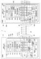
- FIG. 1 is a diagram illustrating an example of the configuration of a digital coherent optical transmission system according to an embodiment.
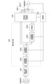
- 2 is a diagram for explaining a detailed configuration of a demodulation digital signal processing unit in the embodiment.
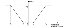
- FIG. FIG. 11 is a diagram showing an example (part 1) of coefficient selection of a step size ⁇ used when updating a filter coefficient of an adaptive equalization unit in the embodiment.
- FIG. 11 is a diagram showing an example (part 2) of coefficient selection of a step size ⁇ used when updating a filter coefficient of an adaptive equalization unit in the embodiment.
- 13 is a diagram for explaining a detailed configuration of a demodulation digital signal processing unit in a modified example.
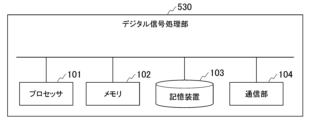
- FIG. FIG. 2 is a diagram illustrating an example of a hardware configuration of a digital signal processing unit according to the embodiment.
- the digital coherent optical transmission system 1 includes a transmitter 10, a WDM multiplexer 20, an optical fiber transmission line 30, a WDM demultiplexer 40, and a receiver 50.
- the transmitter 10 includes one or more transmitting units 100.
- the transmitter 10 includes a number of transmitting units 100 equal to the number of wavelength division multiplexing (WDM) channels.
- the transmitting unit 100 includes a digital signal processing unit 110, a modulator driver 120, a light source 130, and an integrated module 140.
- the digital signal processing unit 110 includes an encoding unit 111, a mapping unit 112, a training signal insertion unit 113, a sampling frequency changing unit 114, a waveform shaping unit 115, a pre-equalization unit 116, and digital-to-analog converters 117-1 to 117-4 (DAC).
- the modulator driver 120 includes amplifiers 121-1 to 121-4.
- the integrated module 140 includes IQ modulators 141-1 and 141-2, and a polarization synthesis unit 142.
- the optical fiber transmission line 30 includes an optical fiber.
- the optical fiber is, for example, a single mode fiber.
- the optical fiber transmission line 30 includes any number of optical amplifiers 31.
- the receiver 50 includes one or more receiving units 500.
- the receiver 50 includes a number of receiving units 500 equal to the number of wavelength division multiplexing (WDM) channels.
- the receiving unit 500 includes a local oscillator light source 510, an optical front end 520, and a digital signal processing unit 530.
- the optical front end 520 includes a polarization splitter 521, optical 90-degree hybrid couplers 522-1 to 522-2, balanced photodiodes 523-1 to 523-4 (BPD: Balanced Photo Diodes), and amplifiers 524-1 to 524-4.
- BPD Balanced Photo Diodes
- the digital signal processing unit 530 includes analog-to-digital converters 531-1 to 531-4 (ADCs), a front-end correction unit 532, a chromatic dispersion compensation unit 533, an adaptive equalization unit 534, a frequency offset compensation unit 535, a demapping unit 536, a decoding unit 537, and a control unit 538.
- ADCs analog-to-digital converters 531-1 to 531-4
- ADCs analog-to-digital converters 531-1 to 531-4
- ADCs analog-to-digital converters 531-1 to 531-4 (ADCs)
- ADCs analog-to-digital converters 531-1 to 531-4
- ADCs analog-to-digital converters 531-1 to 531-4
- ADCs analog-to-digital converters 531-1 to 531-4
- a front-end correction unit 532 includes a front-end correction unit 532, a chromatic dispersion compensation unit 533, an adaptive equalization unit 534,
- the transmitter 10 transmits an optical signal of a polarization multiplexed phase modulated signal (polarization multiplexed optical signal) to the receiver 50.
- each transmitting unit 100 outputs optical signals of mutually different wavelengths to the WDM multiplexer 20.
- the encoding unit 111 performs forward error correction (FEC) encoding on the transmission bit sequence.
- the encoding unit 111 outputs the transmission signal generated by performing the forward error correction encoding to the mapping unit 112.
- the mapping unit 112 maps the transmission signal output from the encoding unit 111 to a symbol.
- the training signal insertion unit 113 inserts a known training signal into the transmission signal that has been mapped to a symbol by the mapping unit 112.
- the sampling frequency change unit 114 changes the sampling frequency of the transmission signal into which the training signal has been inserted.
- the sampling frequency change unit 114 performs upsampling on the transmission signal into which the training signal has been inserted.
- the waveform shaping unit 115 limits the band of the transmission signal into which upsampling has been performed.
- the pre-equalization unit 116 compensates for waveform distortion in the transmission signal whose band has been limited by the waveform shaping unit 115.
- the pre-equalization unit 116 outputs the transmission signal whose waveform distortion has been compensated for to the DACs 117-1 to 117-4.
- DAC 117-1 converts the I component (in-phase component) (real component signal) of the X-polarized wave of the transmission signal (digital signal) input from the pre-equalization unit 116 into an analog signal. DAC 117-1 outputs this analog signal to the modulator driver 120.
- DAC 117-2 converts the Q component (quadrature component) (imaginary component signal) of the X-polarized wave of the transmission signal (digital signal) input from the pre-equalization unit 116 into an analog signal. DAC 117-2 outputs this analog signal to the modulator driver 120.
- DAC 117-3 converts the I component of the Y polarization of the transmission signal (digital signal) input from pre-equalization unit 116 into an analog signal. DAC 117-3 outputs this analog signal to modulator driver 120.
- DAC 117-4 converts the Q component of the Y polarization of the transmission signal (digital signal) input from pre-equalization unit 116 into an analog signal. DAC 117-4 outputs this analog signal to modulator driver 120.
- Amplifier 121-i (i is an integer equal to or greater than 1 and equal to or less than 4) amplifies the power of the analog signal output from DAC 117-i.
- Amplifiers 121-1 to 121-2 use the analog signal with amplified power to drive IQ modulator 141-1 of integrated module 140.
- Amplifiers 121-3 to 121-4 use the analog signal with amplified power to drive IQ modulator 141-2 of integrated module 140.
- the light source 130 is, for example, a laser diode (LD).
- the light source 130 provided in the j-th transmitting unit 100 outputs light of a wavelength “ ⁇ j ” (the subscript “j” is an integer equal to or greater than 1 and equal to or less than the number of WDM channels) to the integrated module 140.
- the IQ modulator 141-1 generates an X-polarized optical signal by modulating the light output from the light source 130 based on the I component of the X-polarized wave output from the amplifier 121-1 and the Q component of the X-polarized wave output from the amplifier 121-2.
- the IQ modulator 141-1 outputs the generated X-polarized optical signal to the polarization combiner 142.
- the IQ modulator 141-2 generates a Y-polarized optical signal by modulating the light output from the light source 130 based on the I component of the Y-polarized wave output from the amplifier 121-3 and the Q component of the Y-polarized wave output from the amplifier 121-4.
- the IQ modulator 141-2 outputs the generated Y-polarized optical signal to the polarization combiner 142.
- the polarization combining unit 142 performs polarization combining on the X-polarized optical signal output from the IQ modulator 141-1 and the Y-polarized optical signal output from the IQ modulator 141-2.
- the polarization combining unit 142 outputs the optical signal after polarization combining to the WDM multiplexer 20.
- the WDM multiplexer 20 multiplexes a plurality of optical signals output from each transmitting unit 100.
- the WDM multiplexer 20 outputs the multiplexed optical signal to the optical fiber transmission line 30.
- the optical fiber transmission line 30 transmits the multiplexed optical signal.
- the optical signals are input to each optical amplifier 31.
- Each optical amplifier 31 amplifies the optical power of the input optical signal.
- Each optical amplifier 31 transmits the optical signal with the amplified optical power toward the WDM demultiplexer 40.
- the WDM demultiplexer 40 demultiplexes the optical signals transmitted through the optical fiber transmission line 30 according to wavelength.
- the receiver 50 receives the polarization multiplexed optical signal from the transmitter 10 via the WDM multiplexer 20, the optical fiber transmission line 30, and the WDM demultiplexer 40.
- each receiver 500 receives the optical signal demultiplexed by the WDM demultiplexer 40.
- the wavelength of the optical signal received by each receiver 500 is different for each receiver 500.
- the local oscillator light source 510 is, for example, a laser diode (LD).
- the local oscillator light source 510 (LO: Local Oscillator) outputs local oscillator light to the optical front end 520.
- the optical front end 520 (coherent receiver) uses the local oscillator light to convert the received optical signal into an electrical signal while maintaining the phase and amplitude of the polarization multiplexed phase modulated signal.
- the polarization separation unit 521 separates the received optical signal into an X-polarized optical signal and a Y-polarized optical signal.
- the polarization separation unit 521 outputs the X-polarized optical signal to the optical 90-degree hybrid coupler 522-1.
- the polarization separation unit 521 outputs the Y-polarized optical signal to the optical 90-degree hybrid coupler 522-2.
- the optical 90-degree hybrid coupler 522-1 extracts the I and Q components of the received optical signal from the optical signal by interfering the local oscillator light output from the local oscillator light source 510 with the X-polarized optical signal.
- the optical 90-degree hybrid coupler 522-1 outputs the extracted I and Q components of the X-polarized wave to the balanced photodiodes 523-1 and 523-2.
- the optical 90-degree hybrid coupler 522-2 extracts the I and Q components of the received optical signal from the optical signal by interfering with the local oscillator light output from the local oscillator light source 510 and the Y-polarized optical signal.
- the optical 90-degree hybrid coupler 522-2 outputs the extracted I and Q components of the Y-polarized wave to the balanced photodiode 523-3 and the balanced photodiode 523-4.
- Balanced photodiodes 523-1 to 523-4 are differential input type photoelectric converters.
- Balanced photodiode 523-i has two photodiodes (not shown) with the same characteristics. Each photodiode (not shown) generates a photocurrent.
- Balanced photodiode 523-i outputs a current equivalent to the difference between the photocurrents to amplifier 524-i.
- Balanced photodiode 523-1 converts the I component of the X polarization of the received optical signal into an electrical signal. Balanced photodiode 523-1 outputs this electrical signal to amplifier 524-1.
- Balanced photodiode 523-2 converts the Q component of the X polarization of the received optical signal into an electrical signal. Balanced photodiode 523-2 outputs this electrical signal to amplifier 524-2.
- Balanced photodiode 523-3 converts the I component of the Y polarization of the received optical signal into an electrical signal. Balanced photodiode 523-3 outputs this electrical signal to amplifier 524-3.
- Balanced photodiode 523-4 converts the Q component of the Y polarization of the received optical signal into an electrical signal. Balanced photodiode 523-4 outputs this electrical signal to amplifier 524-4.
- the front-end correction unit 532 receives the I component signal (real component signal) "XI” of the X polarization of the received signal from ADC 531-1.
- the front-end correction unit 532 receives the Q component signal (imaginary component signal) "XQ” of the X polarization of the received signal from ADC 531-2.
- the front-end correction unit 532 receives the I component signal "YI” of the Y polarization of the received signal from ADC 531-3.
- the front-end correction unit 532 receives the Q component signal "YQ” of the Y polarization of the received signal from ADC 531-4.
- the adaptive equalization unit 534 adaptively performs equalization processing on the received signal output from the chromatic dispersion compensation unit 533 using an adaptive equalization filter.
- the adaptive equalization unit 534 may estimate the value of the frequency offset of the local oscillator light source 510 using, for example, a digital phase-locked loop.
- the frequency offset compensation unit 535 performs a process of compensating for a frequency offset on the received signal on which equalization processing has been adaptively performed by the adaptive equalization unit 534.
- the frequency offset compensation unit 535 may also perform a process of compensating for phase noise on the received signal on which equalization processing has been adaptively performed by the adaptive equalization unit 534.
- the demapping unit 536 determines the symbols of the received signal output from the frequency offset compensation unit 535.
- the demapping unit 536 converts the determined symbols into binary data.
- the decoding unit 537 performs error correction decoding processing (e.g., forward error correction) on the binary data converted by the demapping unit 536. As a result, the decoding unit 537 generates a received bit sequence.
- the control unit 538 estimates the value of the frequency offset of the local oscillator light source 510 using, for example, a digital phase-locked loop.
- the control unit 538 updates the filter coefficients in the adaptive equalization filter used in the adaptive equalization unit 534 based on the value of the frequency offset.
- the control unit 538 calculates an update term for the adaptive equalization filter based on the error between the output of the frequency offset compensation unit 535 and a reference signal (a known signal or a signal after hard decision).
- the adaptive equalization filter is updated using the LMS (Least Mean Square) algorithm or the RLS (Recursive Least Squares) algorithm.
- the control unit 538 controls to change the update step size of the filter coefficients in the adaptive equalization filter used in the adaptive equalization unit 534. Specifically, the control unit 538 controls to stop updating the filter coefficients by making the update step size of the filter coefficients smaller as the frequency offset value becomes smaller. For example, when the frequency offset value is less than a predetermined value, the control unit 538 calculates the update step size using a function that makes the update step size 0, and updates the filter coefficients in the adaptive equalization filter using the calculated update step size.
- the receiver characteristic compensation unit 5341 receives the chromatic dispersion compensated signals S x,out , S x * ,out , S y,out , and S y * ,out output from the chromatic dispersion compensation unit 533.
- the receiver characteristic compensation unit 5341 compensates for waveform distortion occurring in the receiver 50 using a digital filter (e.g., 4 ⁇ 2 MIMO (Multiple Input Multiple Output) configuration) on the input chromatic dispersion compensated signals S x,out , S x * ,out , S y,out , and S y * ,out .
- the receiver characteristic compensation unit 5341 outputs the signals S x,out , S y,out after compensation for waveform distortion occurring in the receiver 50 to the transmission path characteristic compensation unit 5342.
- the filter coefficients of the digital filter used by the receiver characteristic compensation unit 5341 are updated by the control unit 538.
- the control unit 538 calculates an update term for the digital filter, and updates the filter coefficients by multiplying the calculated update term (update portion) by an update step size of the filter coefficient that depends on the value of the frequency offset of the local oscillator light source 510.
- the transmission path characteristic compensating unit 5342 receives as input signals S x,out and S y,out after compensation for waveform distortion occurring in the receiver 50, which are output from the receiver characteristic compensating unit 5341.
- the transmission path characteristic compensating unit 5342 uses a digital filter (e.g., a 2 ⁇ 2 MIMO configuration) on the signals S x,out and S y,out after compensation for waveform distortion occurring in the receiver 50 to compensate for composite distortions such as polarization rotation, polarization mode dispersion, and polarization dependent loss occurring in the transmission path other than chromatic dispersion.
- the transmission path characteristic compensating unit 5342 outputs the signals S x,out and S y,out after compensation for composite distortion.
- the filter coefficients of the digital filter used by the transmission path characteristic compensating unit 5342 are updated by the control unit 538.
- the signals S x,out and S y,out after the composite distortion compensation output from the transmission path characteristic compensation unit 5342 are each split into two paths and input to the frequency offset compensation unit 535 and the transmitter characteristic compensation unit 5343 .
- the transmitter characteristic compensation unit 5343 compensates for waveform distortion occurring in the transmitter by using a digital filter (e.g., a 2 ⁇ 2 MIMO configuration) on the input signals S x,out and S y,out after the composite distortion compensation.
- the transmitter characteristic compensation unit 5343 outputs the signals S x,out and S y,out after the waveform distortion compensation occurring in the transmitter 10 to the conversion unit 5344.
- the filter coefficients of the digital filter used by the transmitter characteristic compensation unit 5343 are updated by the control unit 538.
- the control unit 538 calculates an update term for the digital filter, and updates the filter coefficients by multiplying the calculated update term (update portion) by an update step size of the filter coefficient that depends on the value of the frequency offset of the local oscillation light source 510.
- the converter 5344 receives as input the signals S x,out and S y,out after compensation for waveform distortion occurring in the transmitter 10, which are output from the transmitter characteristic compensation unit 5343.
- the converter 5344 takes the phase conjugate of the input signals S x,out and S y,out after compensation for waveform distortion occurring in the transmitter 10.
- the converter 5344 outputs the phase conjugated signals S x * ,out and S y * ,out to the frequency offset compensation unit 535.
- the frequency offset compensating unit 535 receives as input the signals S x,out , S y,out after the composite distortion compensation output from the transmission path characteristic compensating unit 5342, and the phase conjugate signals S x * ,out , S y * ,out output from the converting unit 5344.
- the frequency offset compensating unit 535 compensates for the frequency offset of the input signals S x,out , S x * ,out , S y,out , and S y * ,out using the frequency offset of the local light estimated by the control unit 538.
- the frequency offset compensating unit 535 outputs the signals S x,out , S x * ,out , S y,out , and S y * ,out after the frequency offset compensation.
- the frequency offset compensated signals S x,out and S x * ,out output from the frequency offset compensation unit 535 are input to the adder 540-1, and the frequency offset compensated signals S y,out and S y * ,out are input to the adder 540-2.
- the adder 540-1 adds the input signals S x,out and S x * ,out .
- the adder 540-2 adds the input signals S y,out and S y * ,out .
- the signals added by the adders 540-1 and 540-2 are demodulated by the decoder 537. As a result, demodulated signals S x,in and S y,in are generated.
- the update step size " ⁇ 0 " of the filter coefficient is 1. Note that the frequency “f a " may be set to the frequency "f b ", and two values, 0 and 1, may be switched between.
- the computer-readable recording medium is, for example, a portable medium such as a flexible disk, a magneto-optical disk, a ROM (Read Only Memory), a CD-ROM (Compact Disc Read Only Memory), or a non-transient recording medium such as a storage device such as a hard disk or a solid state drive (SSD) built into a computer system.
- the communication unit 104 executes a predetermined communication process.
- the digital signal processing unit 530 may be realized using hardware (accelerator) including an electronic circuit (electronic circuit or circuitry) using, for example, an LSI (Large Scale Integrated circuit), an ASIC (Application Specific Integrated Circuit), a PLD (Programmable Logic Device), or an FPGA (Field Programmable Gate Array).
- the present invention is applicable to optical transmission systems.
- 1...digital coherent optical transmission system 5...demodulation digital signal processing unit, 10...transmitter, 20...WDM multiplexer, 30...optical fiber transmission line, 31...optical amplifier, 40...WDM demultiplexer, 50...receiver, 100...transmitter, 110...digital signal processing unit, 111...encoding unit, 112...mapping unit, 113...training signal insertion unit, 114...sampling frequency change unit, 115...waveform shaping unit, 116...pre-equalization unit, 117-1 to 117-4...digital-to-analog converter, 120...modulator driver, 121-1 to 121-4...amplifier, 130...light source, 140...integrated module, 141-1, 141-2...IQ modulator, 142...polarization synthesis unit, 500...receiving unit, 510...local oscillator light source, 520...optical front end, 521...polarization separation unit, 522-1, 522-2...optical 90-degree hybrid coupler, 523-1 to 523-4...balanced
Landscapes
- Physics & Mathematics (AREA)
- Electromagnetism (AREA)
- Engineering & Computer Science (AREA)
- Computer Networks & Wireless Communication (AREA)
- Signal Processing (AREA)
- Optical Communication System (AREA)
Abstract
信号処理装置が実行する信号処理方法であって、送信機から送信された光信号の搬送波の周波数に対する、光信号を受信した受信機の局部発振光源の周波数オフセットを推定し、推定した受信機の局部発振光源の周波数オフセットの値が所定の値未満である場合に、光信号に基づく受信信号に対して等化処理を適応的に実行する送信機で生じる波形歪みを補償する送信機特性補償部で用いる適応等化フィルタ、又は、受信機で生じる波形歪みを補償する受信機特性補償部で用いる適応等化フィルタの少なくともいずれかと、伝送路で生じる波長分散以外の歪みを補償する伝送路特性補償部で用いる適応等化フィルタそれぞれにおけるフィルタ係数の更新ステップサイズを変更するように制御する、信号処理方法。
Description
本発明は、信号処理方法及び信号処理装置に関する。
従来、コヒーレント光受信機における復調性能を向上させる技術として、コヒーレント光受信機内のデジタルフィルタにおいて送受信機内で発生する信号波形歪みを適応的に補償する方式が注目されている。適応フィルタを用いてコヒーレント光受信機内のデジタル信号処理により送信機で生じる信号波形歪み特性を補償する技術は提案されている(例えば、非特許文献1及び2参照)。非特許文献1及び2に記載の技術では、送信機特性補償は受信機特性補償と同時に行われている。
A. Kawai, M. Nakamura, M. Takahashi, T. Kobayashi and Y. Miyamoto, "Partial Freezing for MIMO Adaptive Equalizers: Precise Demodulation in Dynamic Environments", Journal of Ligtwave Technology, doi: 10.1109/JLT.2023.3251996.
C. R. S. Fludger and T. Kupfer, "Transmitter Impairment Mitigation and Monitoring for High Baud-Rate, High Order Modulation Systems", Proc. Eur. Conf. Opt. Commun., 2016, Paper Tu.2.A.2.
しかしながら、コヒーレント光受信機の局部発振光の周波数オフセットが小さい場合(例えば、周波数オフセットが0あるいは0に近い場合)、送信機特性と受信機特性の分離不可能になる。そのため、従来のように、送信機特性と受信機特性の更新を同時に行うと、動作が不安定になることにより光信号の波形歪を安定的に補償することができないという問題がある。
上記事情に鑑み、本発明は、光信号の搬送波の周波数に対して、受信機の局部発振光源の周波数オフセットが小さい場合でも、光信号の波形歪を安定的に補償することができる技術の提供を目的としている。
本発明の一態様は、信号処理装置が実行する信号処理方法であって、送信機から送信された光信号の搬送波の周波数に対する、前記光信号を受信した受信機の局部発振光源の周波数オフセットを推定し、推定した前記受信機の局部発振光源の周波数オフセットの値が所定の値未満である場合に、前記光信号に基づく受信信号に対して等化処理を適応的に実行する前記送信機で生じる波形歪みを補償する送信機特性補償部で用いる適応等化フィルタ、又は、前記受信機で生じる波形歪みを補償する受信機特性補償部で用いる適応等化フィルタの少なくともいずれかと、伝送路で生じる波長分散以外の歪みを補償する伝送路特性補償部で用いる適応等化フィルタそれぞれにおけるフィルタ係数の更新ステップサイズを変更するように制御する、信号処理方法である。
本発明の一態様は、送信機から送信された光信号の搬送波の周波数に対する、前記光信号を受信した受信機の局部発振光源の周波数オフセットを推定し、推定した前記受信機の局部発振光源の周波数オフセットの値が所定の値未満である場合に、前記光信号に基づく受信信号に対して等化処理を適応的に実行する前記送信機で生じる波形歪みを補償する送信機特性補償部で用いる適応等化フィルタ、又は、前記受信機で生じる波形歪みを補償する受信機特性補償部で用いる適応等化フィルタの少なくともいずれかと、伝送路で生じる波長分散以外の歪みを補償する伝送路特性補償部で用いる適応等化フィルタそれぞれにおけるフィルタ係数の更新ステップサイズを変更するように制御する制御部、を備える信号処理装置である。
本発明により、光信号の搬送波の周波数に対して受信機の局部発振光源の周波数オフセットが小さい場合でも、光信号の波形歪を安定的に補償することが可能となる。
以下、本発明の一実施形態を、図面を参照しながら説明する。
図1は、実施形態におけるデジタルコヒーレント光伝送システム1の構成例を示す図である。デジタルコヒーレント光伝送システム1は、送信機10と、WDM合波器20と、光ファイバ伝送路30と、WDM分波器40と、受信機50とを備える。
図1は、実施形態におけるデジタルコヒーレント光伝送システム1の構成例を示す図である。デジタルコヒーレント光伝送システム1は、送信機10と、WDM合波器20と、光ファイバ伝送路30と、WDM分波器40と、受信機50とを備える。
送信機10は、1以上の送信部100を備える。以下では、送信機10は、波長分割多重(WDM)のチャネル数に等しい台数の送信部100を備える。送信部100は、デジタル信号処理部110と、変調器ドライバ120と、光源130と、集積モジュール140とを備える。
デジタル信号処理部110は、符号化部111と、マッピング部112と、トレーニング信号挿入部113と、サンプリング周波数変更部114と、波形整形部115と、予等化部116と、デジタル・アナログ変換器117-1~117-4(DAC)とを備える。変調器ドライバ120は、アンプ121-1~121-4を備える。集積モジュール140は、IQ変調器141-1及び141-2と、偏波合成部142とを備える。
光ファイバ伝送路30は、光ファイバを備える。光ファイバは、例えば、シングルモードファイバである。光ファイバ伝送路30は、任意の台数の光増幅器31を備える。
受信機50は、1以上の受信部500を備える。受信機50は、一例として、波長分割多重(WDM)のチャネル数に等しい台数の受信部500を備える。受信部500は、局部発振光源510と、光フロントエンド520と、デジタル信号処理部530とを備える。
光フロントエンド520は、偏波分離部521と、光90度ハイブリッドカプラ522-1~522-2と、バランスフォトダイオード523-1~523-4(BPD: Balanced Photo Diode)と、アンプ524-1~524-4とを備える。
デジタル信号処理部530は、アナログ・デジタル変換器531-1~531-4(ADC)と、フロントエンド補正部532と、波長分散補償部533と、適応等化部534と、周波数オフセット補償部535と、デマッピング部536と、復号部537と、制御部538とを備える。ここで、デジタル信号処理部530は、フロントエンド補正部532と、波長分散補償部533と、適応等化部534と、周波数オフセット補償部535と、制御部538とを、復調デジタル信号処理部5として備える。
次に、送信機10について説明する。
送信機10は、偏波多重された位相変調信号の光信号(偏波多重光信号)を、受信機50に送信する。ここで、各送信部100は、互いに異なる波長の光信号を、WDM合波器20に出力する。
送信機10は、偏波多重された位相変調信号の光信号(偏波多重光信号)を、受信機50に送信する。ここで、各送信部100は、互いに異なる波長の光信号を、WDM合波器20に出力する。
符号化部111は、送信ビット列に対して、前方誤り訂正(FEC: forward error correction)符号化を実行する。符号化部111は、前方誤り訂正符号化を実行することによって生成された送信信号を、マッピング部112に出力する。マッピング部112は、符号化部111から出力された送信信号を、シンボルにマッピングする。
トレーニング信号挿入部113は、マッピング部112によってシンボルにマッピングされた送信信号に、既知のトレーニング信号を挿入する。サンプリング周波数変更部114は、トレーニング信号が挿入された送信信号のサンプリング周波数を変更する。ここで、サンプリング周波数変更部114は、トレーニング信号が挿入された送信信号に対して、アップサンプリングを実行する。波形整形部115は、アップサンプリングが実行された送信信号の帯域を制限する。
予等化部116は、波形整形部115によって帯域が制限された送信信号の波形歪を補償する。予等化部116は、波形歪が補償された送信信号を、DAC117-1~117-4に出力する。
DAC117-1は、予等化部116から入力された送信信号(デジタル信号)のX偏波のI成分(同相成分)(実数成分信号)を、アナログ信号に変換する。DAC117-1は、このアナログ信号を、変調器ドライバ120に出力する。
DAC117-2は、予等化部116から入力された送信信号(デジタル信号)のX偏波のQ成分(直交成分)(虚数成分信号)を、アナログ信号に変換する。DAC117-2は、このアナログ信号を、変調器ドライバ120に出力する。
DAC117-3は、予等化部116から入力された送信信号(デジタル信号)のY偏波のI成分を、アナログ信号に変換する。DAC117-3は、このアナログ信号を、変調器ドライバ120に出力する。
DAC117-4は、予等化部116から入力された送信信号(デジタル信号)のY偏波のQ成分を、アナログ信号に変換する。DAC117-4は、このアナログ信号を、変調器ドライバ120に出力する。
アンプ121-i(iは、1以上の整数であって、4以下の整数)は、DAC117-iから出力されたアナログ信号のパワーを増幅する。アンプ121-1~121-2は、パワーが増幅されたアナログ信号を用いて、集積モジュール140のIQ変調器141-1を駆動する。アンプ121-3~121-4は、パワーが増幅されたアナログ信号を用いて、集積モジュール140のIQ変調器141-2を駆動する。
光源130は、例えば、レーザーダイオード(LD)である。j番目の送信部100に備えられた光源130は、波長「λj」(添字「j」は、1以上の整数であって、WDMのチャネル数以下の整数)の光を、集積モジュール140に出力する。
IQ変調器141-1は、アンプ121-1から出力されたX偏波のI成分と、アンプ121-2から出力されたX偏波のQ成分とに基づいて、光源130から出力された光を変調することによって、X偏波の光信号を生成する。IQ変調器141-1は、生成されたX偏波の光信号を、偏波合成部142に出力する。
IQ変調器141-2は、アンプ121-3から出力されたY偏波のI成分と、アンプ121-4から出力されたY偏波のQ成分とに基づいて、光源130から出力された光を変調することによって、Y偏波の光信号を生成する。IQ変調器141-2は、生成されたY偏波の光信号を、偏波合成部142に出力する。
偏波合成部142は、IQ変調器141-1から出力されたX偏波の光信号と、IQ変調器141-2から出力されたY偏波の光信号とに対して、偏波合成を実行する。偏波合成部142は、偏波合成が実行された光信号を、WDM合波器20に出力する。
次に、WDM合波器20、光ファイバ伝送路30及びWDM分波器40について説明する。
WDM合波器20は、各送信部100から出力された複数の光信号を合波する。WDM合波器20は、合波された光信号を、光ファイバ伝送路30に出力する。光ファイバ伝送路30は、合波された光信号を伝送する。ここで、光信号は、各光増幅器31に入力される。各光増幅器31は、入力された光信号の光パワーを増幅する。各光増幅器31は、光パワーが増幅された光信号を、WDM分波器40に向けて伝送する。WDM分波器40は、光ファイバ伝送路30を伝送された光信号を、波長に応じて分波する。
WDM合波器20は、各送信部100から出力された複数の光信号を合波する。WDM合波器20は、合波された光信号を、光ファイバ伝送路30に出力する。光ファイバ伝送路30は、合波された光信号を伝送する。ここで、光信号は、各光増幅器31に入力される。各光増幅器31は、入力された光信号の光パワーを増幅する。各光増幅器31は、光パワーが増幅された光信号を、WDM分波器40に向けて伝送する。WDM分波器40は、光ファイバ伝送路30を伝送された光信号を、波長に応じて分波する。
次に、受信機50について説明する。
受信機50は、WDM合波器20と光ファイバ伝送路30とWDM分波器40とを介して、偏波多重光信号を送信機10から受信する。ここで、各受信部500は、WDM分波器40によって分波された光信号を受信する。各受信部500に受信される光信号の波長は、受信部500ごとに異なる。
受信機50は、WDM合波器20と光ファイバ伝送路30とWDM分波器40とを介して、偏波多重光信号を送信機10から受信する。ここで、各受信部500は、WDM分波器40によって分波された光信号を受信する。各受信部500に受信される光信号の波長は、受信部500ごとに異なる。
局部発振光源510は、例えば、レーザーダイオード(LD)である。局部発振光源510(LO: Local Oscillator)は、光フロントエンド520に局部発振光を出力する。光フロントエンド520(コヒーレント受信機)は、局部発振光を用いて、偏波多重された位相変調信号の位相及び振幅を保ったまま、受信された光信号を電気信号に変換する。
偏波分離部521は、受信された光信号を、X偏波の光信号とY偏波の光信号とに分離する。偏波分離部521は、X偏波の光信号を、光90度ハイブリッドカプラ522-1に出力する。偏波分離部521は、Y偏波の光信号を、光90度ハイブリッドカプラ522-2に出力する。
光90度ハイブリッドカプラ522-1は、局部発振光源510から出力された局部発振光とX偏波の光信号とを干渉させることによって、受信された光信号のI成分及びQ成分を、光信号から抽出する。光90度ハイブリッドカプラ522-1は、抽出されたX偏波のI成分及びQ成分を、バランスフォトダイオード523-1及び523-2に出力する。
光90度ハイブリッドカプラ522-2は、局部発振光源510から出力された局部発振光とY偏波の光信号とを干渉させることによって、受信された光信号のI成分及びQ成分を、光信号から抽出する。光90度ハイブリッドカプラ522-2は、抽出されたY偏波のI成分及びQ成分を、バランスフォトダイオード523-3及びバランスフォトダイオード523-4に出力する。
バランスフォトダイオード523-1~523-4は、差動入力型の光電変換器である。バランスフォトダイオード523-iは、同じ特性を有する2個のフォトダイオード(不図示)を備える。各フォトダイオード(不図示)には、光電流がそれぞれ生じる。バランスフォトダイオード523-iは、光電流の差分に相当する電流を、アンプ524-iに出力する。
バランスフォトダイオード523-1は、受信された光信号のX偏波のI成分を、電気信号に変換する。バランスフォトダイオード523-1は、この電気信号をアンプ524-1に出力する。バランスフォトダイオード523-2は、受信された光信号のX偏波のQ成分を、電気信号に変換する。バランスフォトダイオード523-2は、この電気信号をアンプ524-2に出力する。バランスフォトダイオード523-3は、受信された光信号のY偏波のI成分を、電気信号に変換する。バランスフォトダイオード523-3は、この電気信号をアンプ524-3に出力する。バランスフォトダイオード523-4は、受信された光信号のY偏波のQ成分を、電気信号に変換する。バランスフォトダイオード523-4は、この電気信号をアンプ524-4に出力する。
アンプ524-i(iは、1以上の整数であって、4以下の整数)は、バランスフォトダイオード523-iから出力された電気信号のパワーを増幅する。アンプ524-iは、パワーが増幅された電気信号を、デジタル信号処理部530に出力する。
ADC531-iは、アンプ524-iから出力された電気信号(アナログ信号)を、デジタル信号に変換する。ADC531-iは、このデジタル信号を、フロントエンド補正部532に出力する。
フロントエンド補正部532には、受信信号のX偏波のI成分信号(実数成分信号)「XI」が、ADC531-1から入力される。フロントエンド補正部532には、受信信号のX偏波のQ成分信号(虚数成分信号)「XQ」が、ADC531-2から入力される。フロントエンド補正部532には、受信信号のY偏波のI成分信号「YI」が、ADC531-3から入力される。フロントエンド補正部532には、受信信号のY偏波のQ成分信号「YQ」が、ADC531-4から入力される。
フロントエンド補正部532は、入力された各成分を用いて、光フロントエンド520における周波数特性が補償された受信信号を生成する。また、フロントエンド補正部532は、光フロントエンド520における周波数特性が補償された受信信号を、波長分散補償部533に出力する。
波長分散補償部533は、光ファイバ伝送路30において光信号に生じた波長分散を推定する。波長分散補償部533は、フロントエンド補正部532から出力された受信信号に対して、推定された波長分散を補償する処理を実行する。波長分散補償部533は、波長分散を補償する処理が実行された受信信号を、適応等化部534に出力する。
適応等化部534は、波長分散補償部533から出力された受信信号に対して、適応等化フィルタを用いて、等化処理を適応的に実行する。ここで、適応等化部534は、例えばデジタル位相同期回路を用いて、局部発振光源510の周波数オフセットの値を推定してもよい。
周波数オフセット補償部535は、適応等化部534によって等化処理が適応的に実行された受信信号に対して、周波数オフセットを補償する処理を実行する。周波数オフセット補償部535は、適応等化部534によって等化処理が適応的に実行された受信信号に対して、位相ノイズを補償する処理を実行してもよい。
デマッピング部536は、周波数オフセット補償部535から出力された受信信号のシンボルを判定する。デマッピング部536は、判定されたシンボルを、バイナリデータに変換する。復号部537は、デマッピング部536によって変換されたバイナリデータに対して、誤り訂正復号処理(例えば、前方誤り訂正)を実行する。これによって、復号部537は、受信ビット列を生成する。
制御部538は、例えばデジタル位相同期回路を用いて、局部発振光源510の周波数オフセットの値を推定する。制御部538は、周波数オフセットの値に基づいて、適応等化部534で用いる適応等化フィルタにおけるフィルタ係数を更新する。なお、制御部538は、周波数オフセット補償部535の出力と参照信号(既知信号もしくは、硬判定後の信号)との誤差に基づいて適応等化フィルタの更新項を算出する。適応等化フィルタの更新には、LMS(Least Mean Square)アルゴリズムやRLS(Recursive Least Squares)アルゴリズムが用いられる。
さらに、制御部538は、推定した周波数オフセットの値が所定の値未満である場合に、適応等化部534で用いる適応等化フィルタにおけるフィルタ係数の更新ステップサイズを変更するように制御する。具体的には、制御部538は、周波数オフセットの値が小さいほどフィルタ係数の更新ステップサイズを小さくすることによって、フィルタ係数の更新が停止するように制御する。例えば、制御部538は、周波数オフセットの値が所定の値未満である場合に、更新ステップサイズが0となる関数を用いて更新ステップサイズを算出し、算出した更新ステップサイズを用いて適応等化フィルタにおけるフィルタ係数を更新する。
図2は、実施形態における復調デジタル信号処理部5の詳細な構成を説明するための図である。図2では、復調デジタル信号処理部5を構成する適応等化部534の構成を詳細に示している。復調デジタル信号処理部5に入力される受信信号としては、例えば受信信号の各偏波成分とその時間領域の位相共役成分の組としてよいし、受信信号の各偏波成分の実部と虚部の組としても良い。図2では、X偏波成分の信号Sx,outと、X偏波成分の複素共役信号Sx
*
,outと、Y偏波成分の信号Sy,outと、Y偏波成分の複素共役信号Sy
*
,outとが入力されている例を示している。
波長分散補償部533は、入力された各信号Sx,out、Sx
*
,out、Sy,out、Sy
*
,outとに対して波長分散を補償する処理を実行する。波長分散補償部533は、波長分散補償後の信号Sx,out、Sx
*
,out、Sy,out、Sy
*
,outを適応等化部534に出力する。適応等化部534は、受信機特性補償部5341と、伝送路特性補償部5342と、送信機特性補償部5343と、変換部5344とを備える。
受信機特性補償部5341は、波長分散補償部533から出力された波長分散補償後の信号Sx,out、Sx
*
,out、Sy,out、Sy
*
,outを入力とする。受信機特性補償部5341は、入力した波長分散補償後の信号Sx,out、Sx
*
,out、Sy,out、Sy
*
,outに対してデジタルフィルタ(例えば4×2 MIMO(Multiple Input Multiple Output)構成)を用いて、受信機50で生じる波形歪みを補償する。受信機特性補償部5341は、受信機50で生じる波形歪み補償後の信号Sx,out、Sy,outを伝送路特性補償部5342に出力する。
受信機特性補償部5341が用いるデジタルフィルタのフィルタ係数は、制御部538によって更新される。例えば、受信機特性補償部5341が用いるデジタルフィルタのフィルタ係数の更新では、制御部538がデジタルフィルタの更新項を算出し、算出した更新項(更新部分)に、局部発振光源510の周波数オフセットの値に依存するフィルタ係数の更新ステップサイズを乗算することによってフィルタ係数を更新する。
伝送路特性補償部5342は、受信機特性補償部5341から出力された受信機50で生じる波形歪み補償後の信号Sx,out、Sy,outを入力とする。伝送路特性補償部5342は、受信機50で生じる波形歪み補償後の信号Sx,out、Sy,outに対してデジタルフィルタ(例えば2×2 MIMO構成)を用いて、波長分散以外の伝送路で生じる偏波回転、偏波モード分散、偏波依存損失などの複合歪みを補償する。伝送路特性補償部5342は、複合歪み補償後の信号Sx,out、Sy,outを出力する。伝送路特性補償部5342が用いるデジタルフィルタのフィルタ係数は、制御部538によって更新される。
伝送路特性補償部5342から出力された複合歪み補償後の信号Sx,out、Sy,outはそれぞれ、2つの経路に分割されて周波数オフセット補償部535と送信機特性補償部5343とに入力される。
送信機特性補償部5343は、入力した複合歪み補償後の信号Sx,out、Sy,outに対してデジタルフィルタ(例えば2×2 MIMO構成)を用いて、送信機で生じる波形歪みを補償する。送信機特性補償部5343は、送信機10で生じる波形歪み補償後の信号Sx,out、Sy,outを変換部5344に出力する。
送信機特性補償部5343が用いるデジタルフィルタのフィルタ係数は、制御部538によって更新される。例えば、送信機特性補償部5343が用いるデジタルフィルタのフィルタ係数の更新では、制御部538がデジタルフィルタの更新項を算出し、算出した更新項(更新部分)に、局部発振光源510の周波数オフセットの値に依存するフィルタ係数の更新ステップサイズを乗算することによってフィルタ係数を更新する。
変換部5344は、送信機特性補償部5343から出力された送信機10で生じる波形歪み補償後の信号Sx,out、Sy,outを入力とする。変換部5344は、入力した送信機10で生じる波形歪み補償後の信号Sx,out、Sy,outの位相共役をとる。変換部5344は、位相共役をとった信号Sx
*
,out、Sy
*
,outを周波数オフセット補償部535に出力する。
周波数オフセット補償部535は、伝送路特性補償部5342から出力された複合歪み補償後の信号Sx,out、Sy,outと、変換部5344から出力された位相共役をとった信号Sx
*
,out、Sy
*
,outとを入力とする。周波数オフセット補償部535は、入力した信号Sx,out、Sx
*
,out、Sy,out、Sy
*
,outに対して、制御部538で推定した局発光の周波数オフセットを用いて周波数オフセットを補償する。周波数オフセット補償部535は、周波数オフセット補償後の信号Sx,out、Sx
*
,out、Sy,out、Sy
*
,outを出力する。
周波数オフセット補償部535から出力された周波数オフセット補償後の信号Sx,out、Sx
*
,outは加算部540-1に入力され、周波数オフセット補償後の信号Sy,out、Sy
*
,outは加算部540-2に入力される。加算部540-1は、入力した信号Sx,outと信号Sx
*
,outとを加算する。加算部540-2は、入力した信号Sy,outと信号Sy
*
,outとを加算する。加算部540-1及び540-2によって加算された信号は、復号部537により復調される。それによって復調信号Sx,inとSy,inとが生成される。
制御部538は、復調信号Sx,inと復調信号Sy,inを用いて局部発振光源510の周波数オフセットの値を推定する。制御部538は、周波数オフセットの値に基づいて、適応等化部534で用いる適応等化フィルタのフィルタ係数を更新する。例えば、制御部538は、送信機特性補償部5343で用いるデジタルフィルタ、又は、受信機特性補償部5341で用いるデジタルフィルタの少なくともいずれかと、伝送路特性補償部5342で用いるデジタルフィルタそれぞれのフィルタ係数を更新する。このように、制御部538は、3通りのいずれかの組み合わせでフィルタ係数を更新する。
3通りの組み合わせは、以下の通りである。
・送信機特性補償部5343で用いるデジタルフィルタと、伝送路特性補償部5342で用いるデジタルフィルタの組み合わせ
・受信機特性補償部5341で用いるデジタルフィルタと、伝送路特性補償部5342で用いるデジタルフィルタの組み合わせ
・送信機特性補償部5343で用いるデジタルフィルタと、受信機特性補償部5341で用いるデジタルフィルタと、伝送路特性補償部5342で用いるデジタルフィルタの組み合わせ
・送信機特性補償部5343で用いるデジタルフィルタと、伝送路特性補償部5342で用いるデジタルフィルタの組み合わせ
・受信機特性補償部5341で用いるデジタルフィルタと、伝送路特性補償部5342で用いるデジタルフィルタの組み合わせ
・送信機特性補償部5343で用いるデジタルフィルタと、受信機特性補償部5341で用いるデジタルフィルタと、伝送路特性補償部5342で用いるデジタルフィルタの組み合わせ
更新の際には現在の伝達関数に更新分の関数にステップサイズμを乗算した項が足し合わされることにより更新が行われるが、本発明では送信機特性補償部5343又は受信機特性補償部5341いずれかの更新分の関数に周波数オフセットの推定値が0に近い場合に0となるようなステップサイズμを乗算する。
なお、ステップサイズを可変にする代わりに、それと等価になるような処理を行えるようにしてもよい。例えば、更新分の関数を算出する際に用いる入力信号、復調誤差、周波数オフセット成分等や更新分の関数の大きさを周波数オフセット推定値に合わせて変化させてもよい。
図3は、実施形態における適応等化部534のフィルタ係数更新時に用いるステップサイズμの係数選択の一例(その1)を示す図である。図3において、横軸は局部発振光の周波数オフセットfを表し、縦軸は係数μを表す。
周波数オフセット「f」の閾値として、周波数「fa」及び周波数「fb」が定められる。ここで、周波数「fb」の絶対値は、周波数「fa」の絶対値以上である。周波数オフセット「f」の絶対値|f|が周波数「fa」の絶対値未満である場合、フィルタ係数の更新ステップサイズ「μ0」は、0である。周波数オフセット「f」の絶対値|f|が、周波数「fa」の絶対値以上、且つ、周波数「fb」の絶対値未満である場合、フィルタ係数の更新ステップサイズ「μ0」は、周波数オフセット「f」の絶対値|f|に比例する。周波数オフセット「f」の絶対値|f|が周波数「fb」の絶対値以上である場合、フィルタ係数の更新ステップサイズ「μ0」は、1である。なお、周波数「fa」=周波数「fb」とし、0と1の2値を切り替える構成を取っても良い。
図4は、実施形態における適応等化部534のフィルタ係数更新時に用いるステップサイズμの係数選択の一例(その2)を示す図である。図4において、横軸は局部発振光の周波数オフセットfを表し、縦軸は係数μを表す。
図4に示すように、周波数オフセット「f」の絶対値|f|が0に近いほど更新ステップサイズ「μ0」が0に近くなる関数であって、周波数オフセット「f」の絶対値|f|が大きいほど更新ステップサイズ「μ0」が1に漸近する関数を用いて、更新ステップサイズ「μ0」と、周波数オフセット「f」の絶対値|f|との関係が定められてもよい。この関数は、例えば、双曲線正接関数又はシグモイド関数である。これらの関数は、グラフにおける周波数方向及び更新ステップサイズ方向のそれぞれに、定数シフトされてもよい。なお、周波数オフセット「f」の絶対値|f|が周波数「fa」未満の場合は0、周波数オフセット「f」の絶対値|f|が周波数「fb」以上の場合は1とするような閾値処理を行っても良い。
以上のように構成された受信機50によれば、制御部538が、送信機10から送信された光信号の搬送波の周波数に対する、光信号を受信した受信機50の局部発振光源510の周波数オフセットを推定し、推定した受信機50の局部発振光源の周波数オフセットの値が所定の値未満である場合に、光信号に基づく受信信号に対して等化処理を適応的に実行する適応等化フィルタにおけるフィルタ係数の更新が停止するように制御する。このように、光信号の搬送波の周波数に対して受信機の局部発振光源の周波数オフセットが小さい場合には、送信機特性補償部5343で用いるデジタルフィルタ、又は、受信機特性補償部5341で用いるデジタルフィルタの少なくともいずれかと、伝送路特性補償部5342で用いるデジタルフィルタそれぞれのフィルタ係数の更新ステップサイズを変更するように制御する。例えば、制御部538が、フィルタ係数の更新を停止するように制御する。すなわち、送信機特性と受信機特性の更新が行われなくなる。したがって、動作が不安定になることを抑制することができる。そのため、光信号の搬送波の周波数に対して受信機の局部発振光源の周波数オフセットが小さい場合でも、光信号の波形歪を安定的に補償することが可能になる。
さらに、制御部538は、フィルタ係数の更新が停止するように、周波数オフセットの値が小さいほど更新ステップサイズ「μ0」を小さくする。例えば、周波数オフセットの値が所定の値(0あるいは0に近い値(例えば、周波数「fa」))未満である場合に、更新ステップサイズが0となる関数を用いて更新ステップサイズ「μ0」を算出する。これにより、周波数オフセットの値が0になれば、更新ステップサイズ「μ0」の値も0になる。その結果、フィルタ係数の更新を停止させることができる。これによって、適応等化フィルタの係数の自由度が過剰に大きくならないように制限されるため、光信号の搬送波の周波数に対して、受信機の局部発振光源の周波数オフセット(絶対値)が小さい場合でも、光信号の波形歪を安定的に補償することが可能である。
(変形例)
上述した実施形態では、送信機特性補償部5343の後段に周波数オフセット補償部535が備えられる構成を示したが、図5に示すように周波数オフセット補償部535の後段に送信機特性補償部5343が備えられてもよい。図5は、変形例における復調デジタル信号処理部5の詳細な構成を説明するための図である。図5に示すように構成される場合、伝送路特性補償部5342は、複合歪み補償後の信号Sx,out、Sy,outを周波数オフセット補償部535に出力する。
上述した実施形態では、送信機特性補償部5343の後段に周波数オフセット補償部535が備えられる構成を示したが、図5に示すように周波数オフセット補償部535の後段に送信機特性補償部5343が備えられてもよい。図5は、変形例における復調デジタル信号処理部5の詳細な構成を説明するための図である。図5に示すように構成される場合、伝送路特性補償部5342は、複合歪み補償後の信号Sx,out、Sy,outを周波数オフセット補償部535に出力する。
周波数オフセット補償部535は、伝送路特性補償部5342から出力された複合歪み補償後の信号Sx,out、Sy,outを入力とする。周波数オフセット補償部535は、入力した信号Sx,out、Sy,outに対して、制御部538で推定した局発光の周波数オフセットを用いて周波数オフセットを補償する。周波数オフセット補償部535は、周波数オフセット補償後の信号Sx,out、Sy,outを送信機特性補償部5343に出力する。
送信機特性補償部5343は、周波数オフセット補償部535から出力された周波数オフセット補償後の信号Sx,out、Sy,outを入力とする。送信機特性補償部5343は、入力した周波数オフセット補償後の信号Sx,out、Sy,outに対してデジタルフィルタ(例えば2×2 MIMO構成)を用いて、送信機で生じる波形歪みを補償する。送信機特性補償部5343は、送信機10で生じる波形歪み補償後の信号Sx,out、Sy,outを出力する。
(ハードウェア構成)
図6は、実施形態におけるデジタル信号処理部530(信号処理装置)のハードウェア構成例を示す図である。デジタル信号処理部530は、CPU(Central Processing Unit)等のプロセッサ101が、不揮発性の記録媒体(非一時的な記録媒体)を有する記憶装置103とメモリ102とに記憶されたプログラムを実行することにより、ソフトウェアとして実現される。プログラムは、コンピュータ読み取り可能な記録媒体に記録されてもよい。コンピュータ読み取り可能な記録媒体とは、例えばフレキシブルディスク、光磁気ディスク、ROM(Read Only Memory)、CD-ROM(Compact Disc Read Only Memory)等の可搬媒体、コンピュータシステムに内蔵されるハードディスク又はソリッド・ステート・ドライブ(SSD: Solid State Drive)等の記憶装置などの非一時的な記録媒体である。通信部104は、所定の通信処理を実行する。
図6は、実施形態におけるデジタル信号処理部530(信号処理装置)のハードウェア構成例を示す図である。デジタル信号処理部530は、CPU(Central Processing Unit)等のプロセッサ101が、不揮発性の記録媒体(非一時的な記録媒体)を有する記憶装置103とメモリ102とに記憶されたプログラムを実行することにより、ソフトウェアとして実現される。プログラムは、コンピュータ読み取り可能な記録媒体に記録されてもよい。コンピュータ読み取り可能な記録媒体とは、例えばフレキシブルディスク、光磁気ディスク、ROM(Read Only Memory)、CD-ROM(Compact Disc Read Only Memory)等の可搬媒体、コンピュータシステムに内蔵されるハードディスク又はソリッド・ステート・ドライブ(SSD: Solid State Drive)等の記憶装置などの非一時的な記録媒体である。通信部104は、所定の通信処理を実行する。
デジタル信号処理部530は、例えば、LSI(Large Scale Integrated circuit)、ASIC(Application Specific Integrated Circuit)、PLD(Programmable Logic Device)又はFPGA(Field Programmable Gate Array)等を用いた電子回路(electronic circuit又はcircuitry)を含むハードウェア(アクセラレータ)を用いて実現されてもよい。
以上、この発明の実施形態について図面を参照して詳述してきたが、具体的な構成はこの実施形態に限られるものではなく、この発明の要旨を逸脱しない範囲の設計等も含まれる。
本発明は、光伝送システムに適用可能である。
1…デジタルコヒーレント光伝送システム、5…復調デジタル信号処理部、10…送信機、20…WDM合波器、30…光ファイバ伝送路、31…光増幅器、40…WDM分波器、50…受信機、100…送信部、110…デジタル信号処理部、111…符号化部、112…マッピング部、113…トレーニング信号挿入部、114…サンプリング周波数変更部、115…波形整形部、116…予等化部、117-1~117-4…デジタル・アナログ変換器、120…変調器ドライバ、121-1~121-4…アンプ、130…光源、140…集積モジュール、141-1、141-2…IQ変調器、142…偏波合成部、500…受信部、510…局部発振光源、520…光フロントエンド、521…偏波分離部、522-1、522-2…光90度ハイブリッドカプラ、523-1~523-4…バランスフォトダイオード、524-1~524-4…アンプ、530…デジタル信号処理部、531-1~531-4…アナログ・デジタル変換器、532…フロントエンド補正部、533…波長分散補償部、534…適応等化部、535…周波数オフセット補償部、536…デマッピング部、537…復号部、538…制御部、5341…受信機特性補償部、5342…伝送路特性補償部、5343…送信機特性補償部、5344…変換部
Claims (4)
- 信号処理装置が実行する信号処理方法であって、
送信機から送信された光信号の搬送波の周波数に対する、前記光信号を受信した受信機の局部発振光源の周波数オフセットを推定し、
推定した前記受信機の局部発振光源の周波数オフセットの値が所定の値未満である場合に、前記光信号に基づく受信信号に対して等化処理を適応的に実行する前記送信機で生じる波形歪みを補償する送信機特性補償部で用いる適応等化フィルタ、又は、前記受信機で生じる波形歪みを補償する受信機特性補償部で用いる適応等化フィルタの少なくともいずれかと、伝送路で生じる波長分散以外の歪みを補償する伝送路特性補償部で用いる適応等化フィルタそれぞれにおけるフィルタ係数の更新ステップサイズを変更するように制御する、
信号処理方法。 - 前記フィルタ係数の更新では、前記周波数オフセットの絶対値が小さいほど前記フィルタ係数の更新ステップサイズを小さくする、
請求項1に記載の信号処理方法。 - 前記フィルタ係数の更新では、前記周波数オフセットの絶対値が前記所定の値未満である場合に、前記更新ステップサイズが0となる関数が用いられる、
請求項2に記載の信号処理方法。 - 送信機から送信された光信号の搬送波の周波数に対する、前記光信号を受信した受信機の局部発振光源の周波数オフセットを推定し、推定した前記受信機の局部発振光源の周波数オフセットの値が所定の値未満である場合に、前記光信号に基づく受信信号に対して等化処理を適応的に実行する前記送信機で生じる波形歪みを補償する送信機特性補償部で用いる適応等化フィルタ、又は、前記受信機で生じる波形歪みを補償する受信機特性補償部で用いる適応等化フィルタの少なくともいずれかと、伝送路で生じる波長分散以外の歪みを補償する伝送路特性補償部で用いる適応等化フィルタそれぞれにおけるフィルタ係数の更新ステップサイズを変更するように制御する制御部、
を備える信号処理装置。
Priority Applications (2)
| Application Number | Priority Date | Filing Date | Title |
|---|---|---|---|
| JP2025530886A JPWO2025009100A1 (ja) | 2023-07-05 | 2023-07-05 | |
| PCT/JP2023/024935 WO2025009100A1 (ja) | 2023-07-05 | 2023-07-05 | 信号処理方法及び信号処理装置 |
Applications Claiming Priority (1)
| Application Number | Priority Date | Filing Date | Title |
|---|---|---|---|
| PCT/JP2023/024935 WO2025009100A1 (ja) | 2023-07-05 | 2023-07-05 | 信号処理方法及び信号処理装置 |
Publications (1)
| Publication Number | Publication Date |
|---|---|
| WO2025009100A1 true WO2025009100A1 (ja) | 2025-01-09 |
Family
ID=94171756
Family Applications (1)
| Application Number | Title | Priority Date | Filing Date |
|---|---|---|---|
| PCT/JP2023/024935 Ceased WO2025009100A1 (ja) | 2023-07-05 | 2023-07-05 | 信号処理方法及び信号処理装置 |
Country Status (2)
| Country | Link |
|---|---|
| JP (1) | JPWO2025009100A1 (ja) |
| WO (1) | WO2025009100A1 (ja) |
Citations (3)
| Publication number | Priority date | Publication date | Assignee | Title |
|---|---|---|---|---|
| JP2013223128A (ja) * | 2012-04-17 | 2013-10-28 | Nippon Telegr & Teleph Corp <Ntt> | デジタルコヒーレント受信機およびデジタルコヒーレント受信方法 |
| WO2020175014A1 (ja) * | 2019-02-28 | 2020-09-03 | 日本電信電話株式会社 | 信号処理方法、信号処理装置及び通信システム |
| WO2023073927A1 (ja) * | 2021-10-29 | 2023-05-04 | 日本電気株式会社 | デジタル信号処理回路、方法、受信機、及び通信システム |
-
2023
- 2023-07-05 JP JP2025530886A patent/JPWO2025009100A1/ja active Pending
- 2023-07-05 WO PCT/JP2023/024935 patent/WO2025009100A1/ja not_active Ceased
Patent Citations (3)
| Publication number | Priority date | Publication date | Assignee | Title |
|---|---|---|---|---|
| JP2013223128A (ja) * | 2012-04-17 | 2013-10-28 | Nippon Telegr & Teleph Corp <Ntt> | デジタルコヒーレント受信機およびデジタルコヒーレント受信方法 |
| WO2020175014A1 (ja) * | 2019-02-28 | 2020-09-03 | 日本電信電話株式会社 | 信号処理方法、信号処理装置及び通信システム |
| WO2023073927A1 (ja) * | 2021-10-29 | 2023-05-04 | 日本電気株式会社 | デジタル信号処理回路、方法、受信機、及び通信システム |
Also Published As
| Publication number | Publication date |
|---|---|
| JPWO2025009100A1 (ja) | 2025-01-09 |
Similar Documents
| Publication | Publication Date | Title |
|---|---|---|
| JP7128420B2 (ja) | 信号処理方法、信号処理装置及び通信システム | |
| US10148363B2 (en) | Iterative nonlinear compensation | |
| JP6135415B2 (ja) | 非線形歪み補償装置及び方法並びに光受信器 | |
| Torbatian et al. | Performance oriented DSP for flexible long haul coherent transmission | |
| JP6288143B2 (ja) | コヒーレント光受信装置 | |
| US8942573B2 (en) | Blind equalization algorithms for adaptive polarization recovery and PMD compensation | |
| Tabares et al. | Coherent ultra-dense WDM-PON enabled by complexity-reduced digital transceivers | |
| JP6636884B2 (ja) | 光送信機、光伝送システム及び光受信機 | |
| JP7678372B2 (ja) | 特性計測装置、特性計測方法及びコンピュータプログラム | |
| JP7583332B2 (ja) | 信号処理方法、信号処理装置及び通信システム | |
| WO2025009100A1 (ja) | 信号処理方法及び信号処理装置 | |
| JP7758972B2 (ja) | 信号処理方法、信号処理装置及び通信システム | |
| Zhang et al. | Training symbol-based equalization for quadrature duobinary PDM-FTN systems | |
| Kikuchi et al. | FPGA prototyping of single-polarization 112-Gb/s transceiver for optical multilevel signaling with intensity and delay detection | |
| US11736199B1 (en) | Systems and methods for phase compensation | |
| JP7755211B2 (ja) | 信号処理装置、信号処理方法及びコンピュータプログラム | |
| WO2025009105A1 (ja) | 信号処理方法及び信号処理装置 | |
| Kodama et al. | Decision-directed CPR-assisted IQ imbalance-multiplexing for coherent PON downlink system with access-span length difference | |
| US12250101B1 (en) | Coherent optical module for short reach communications | |
| JP7758971B2 (ja) | 信号処理方法、信号処理装置及び通信システム | |
| JP7791486B2 (ja) | マルチキャリア信号波形等化回路及びマルチキャリア信号波形等化方法 | |
| US12470300B1 (en) | Receiver compensation for low extinction ratio at transmitter | |
| Huang et al. | Cascaded MIMO Equalizer for Transceiver IQ Imbalance Compensation in Ultra-High-Order QAM Coherent Optical Transmission | |
| WO2025041341A1 (ja) | 信号処理装置、通信システム及び信号処理方法 | |
| WO2024257279A1 (ja) | 信号処理装置、信号処理方法及び通信システム |
Legal Events
| Date | Code | Title | Description |
|---|---|---|---|
| 121 | Ep: the epo has been informed by wipo that ep was designated in this application |
Ref document number: 23944351 Country of ref document: EP Kind code of ref document: A1 |
|
| ENP | Entry into the national phase |
Ref document number: 2025530886 Country of ref document: JP Kind code of ref document: A |
|
| WWE | Wipo information: entry into national phase |
Ref document number: 2025530886 Country of ref document: JP |
|
| NENP | Non-entry into the national phase |
Ref country code: DE |