WO2025009053A1 - 量子変換器及び量子変換方法 - Google Patents
量子変換器及び量子変換方法 Download PDFInfo
- Publication number
- WO2025009053A1 WO2025009053A1 PCT/JP2023/024748 JP2023024748W WO2025009053A1 WO 2025009053 A1 WO2025009053 A1 WO 2025009053A1 JP 2023024748 W JP2023024748 W JP 2023024748W WO 2025009053 A1 WO2025009053 A1 WO 2025009053A1
- Authority
- WO
- WIPO (PCT)
- Prior art keywords
- film
- quantum
- ferromagnetic
- topological insulator
- stack
- Prior art date
- Legal status (The legal status is an assumption and is not a legal conclusion. Google has not performed a legal analysis and makes no representation as to the accuracy of the status listed.)
- Ceased
Links
Images




Classifications
-
- G—PHYSICS
- G01—MEASURING; TESTING
- G01R—MEASURING ELECTRIC VARIABLES; MEASURING MAGNETIC VARIABLES
- G01R15/00—Details of measuring arrangements of the types provided for in groups G01R17/00 - G01R29/00, G01R33/00 - G01R33/26 or G01R35/00
- G01R15/14—Adaptations providing voltage or current isolation, e.g. for high-voltage or high-current networks
- G01R15/24—Adaptations providing voltage or current isolation, e.g. for high-voltage or high-current networks using light-modulating devices
-
- G—PHYSICS
- G06—COMPUTING OR CALCULATING; COUNTING
- G06N—COMPUTING ARRANGEMENTS BASED ON SPECIFIC COMPUTATIONAL MODELS
- G06N10/00—Quantum computing, i.e. information processing based on quantum-mechanical phenomena
Definitions
- This disclosure relates to a quantum converter and a quantum conversion method.
- Quantum converters for quantum conversion have also been proposed.
- the objective of this disclosure is to provide a quantum converter and a quantum conversion method that can improve conversion efficiency.
- a quantum converter comprising a stack including a topological insulator film and a ferromagnetic film stacked on top of each other, the stack having an interface between the topological insulator film and the ferromagnetic film, a magnetic field application unit that applies a magnetic field including a component perpendicular to the interface to the stack, and a microwave transceiver unit that transmits and receives microwaves to and from the stack, in which laser light is irradiated onto the interface of the stack.
- This disclosure makes it possible to improve conversion efficiency.
- FIG. 1 is a schematic diagram showing a quantum converter according to a first reference example.
- FIG. 2 is a schematic diagram showing a quantum converter according to a second reference example.
- FIG. 3 is a schematic diagram showing a quantum converter according to the first embodiment.
- FIG. 4 is a schematic diagram showing a quantum converter according to the second embodiment.
- FIG. 5 is a diagram showing the relationship between the thickness of the ferromagnetic film, the number of topological insulator films, and the ratio of conversion efficiencies.
- FIG. 6 is a schematic diagram showing a quantum converter according to the third embodiment.
- FIG. 7 is a schematic diagram showing a quantum converter according to the fourth embodiment.
- Fig. 1 is a schematic diagram showing a quantum converter according to the first reference example.
- the quantum converter 100X has a microwave resonator 30, a laminate 10X, an S pole 51, an N pole 52, and an antenna 40.
- the laminate 10X includes a ferromagnetic topological insulator film 11X and a first film 12X.
- the ferromagnetic topological insulator film 11X has a first surface 11XA and a second surface 11XB opposite to the first surface 11XA.
- the first film 12X is in contact with the first surface 11XA.
- the first film 12X is made of, for example, a nonmagnetic insulator.
- the first film 12X is a substrate including, for example, SrTiO 3 , InP, or Al 2 O 3 , or any combination thereof.
- the ferromagnetic topological insulator film 11X includes a topological insulator and a ferromagnetic material doped into the topological insulator.
- the topological insulator includes Bi, Sb, and Te
- the ferromagnetic material includes Cr or V, or both of these.
- the composition of the ferromagnetic topological insulator film 11X is, for example, Crx ( Bi1-ySby ) 2- xTe3 or Vx ( Bi1-ySby ) 2- xTe3 .
- the value of x is 0.1 or more and 0.6 or less
- the value of y is 0.7 or more and 0.9 or less.
- the thickness of the ferromagnetic topological insulator film 11X is, for example, 5 nm or more and 100 ⁇ m or less.
- the ferromagnetic topological insulator film 11X has a square planar shape with a side length of about 1 mm when viewed from a direction perpendicular to the first surface 11XA.
- the planar shape of the ferromagnetic topological insulator film 11X is not limited to a square shape, and may be a circle or the like.
- the south pole 51 and north pole 52 are provided on the outer wall surface of the microwave resonator 30.
- the south pole 51 faces the first surface 11XA
- the north pole 52 faces the second surface 11XB.
- a magnetic field H is generated between the south pole 51 and the north pole 52, oriented from the south pole 51 to the north pole 52.
- the south pole 51 and the north pole 52 act as magnetic field application units and apply a magnetic field H including a component perpendicular to the first surface 11XA to the ferromagnetic topological insulator film 11X.
- the antenna 40 is provided on the outer wall surface of the microwave resonator 30.
- the antenna 40 serves as a microwave transmitting/receiving unit, transmitting and receiving microwaves between the ferromagnetic topological insulator film 11X.
- the microwave resonator 30 is provided with an inlet 31 and an outlet 32.
- the inlet 31 faces the first surface 11XA
- the outlet 32 faces the second surface 11XB.
- An optical fiber is connected to the inlet 31, and laser light L1 is irradiated from the outside toward the ferromagnetic topological insulator film 11X through the inlet 31.
- the laser light L1 is irradiated toward the first surface 11XA of the ferromagnetic topological insulator film 11X.
- An optical fiber is connected to the outlet 32, and the laser light L2 that has passed through the ferromagnetic topological insulator film 11X is output to the outside through the outlet 32.
- the laser light L1 is linearly polarized laser light.
- the polarization and other characteristics of the laser light L2 outputted to the outside through the output port 32 are detected.
- the microwave photons of the microwaves irradiated to the ferromagnetic topological insulator film 11X through the antenna 40 are quantum converted into optical photons.
- the photon conversion efficiency ⁇ of a ferromagnetic material utilizing the Faraday effect is approximately expressed as "A ⁇ F 2 /N S .”
- A is a coefficient determined by the intensity of the laser light
- ⁇ F is the Faraday rotation angle
- N S is the total number of spins contained in the ferromagnetic material.
- the value of A is, for example, about 10 10 .
- the Faraday rotation angle ⁇ F in a ferromagnetic topological insulator film is expressed as "tan -1 ⁇ (rad)."
- ⁇ is the fine structure constant, and the value of "tan -1 ⁇ (rad),” that is, the Faraday rotation angle ⁇ F, is approximately 1/137 rad.
- the total number of spins N S contained in the ferromagnetic topological insulator film 11X is "n S ⁇ V," where n S (mm -3 ) is the spin density per unit volume of the ferromagnetic topological insulator film 11X and V (mm 3 ) is the volume of the ferromagnetic topological insulator film 11X.
- n S0 ( mm -3 ) is the spin density per unit volume of the ferromagnetic material contained in the ferromagnetic topological insulator film 11X and ⁇ S is the atomic ratio of the ferromagnetic material in the ferromagnetic topological insulator film 11X
- the spin density n S per unit volume of the ferromagnetic topological insulator film 11X is " ⁇ S ⁇ n S0 (mm -3 ).
- the spin density nS of the ferromagnetic topological insulator film 11X is calculated as follows.
- ( Bi0.1Sb0.9 ) 2Te3 40 atomic % is Bi or Sb .
- Cr0.15 ( Bi0.1Sb0.9 ) 1.85Te3 15 atomic % of Bi or Sb contained in ( Bi0.1Sb0.9 ) 2Te3 is replaced with Cr. Therefore, the atomic ratio of Cr in Cr0.15(Bi0.1Sb0.9)1.85Te3 is 6 atomic % .
- the spin density per unit volume of Cr is n S0,Cr
- the spin density n S of the ferromagnetic topological insulator film 11X when the composition is Cr 0.15 (Bi 0.1 Sb 0.9 ) 1.85 Te 3 is "0.06 ⁇ n S0,Cr (mm -3 )".
- the conversion efficiency ⁇ TIX of the ferromagnetic topological insulator film 11X when the composition is Cr 0.15 (Bi 0.1 Sb 0.9 ) 1.85 Te 3 is expressed as "A (1/137) 2 / (0.06 ⁇ n S0,Cr ⁇ V)".
- the spin density n S0,Cr is the same as the spin density of yttrium iron garnet (YIG), it is 2.1 ⁇ 10 19 mm -3 . Therefore, when the thickness d of the ferromagnetic topological insulator film 11X is 30 nm and the area S of the first surface 11XA is 1 mm 2 , the conversion efficiency ⁇ TIX of the ferromagnetic topological insulator film 11X is about 1.4 ⁇ 10 ⁇ 8 .
- FIG. 2 is a schematic diagram showing a quantum converter according to the second reference example.
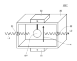
- the quantum converter 100Y according to the second reference example has a ferromagnetic sphere 10Y instead of the laminate 10X.
- the sphere 10Y is made of YIG and has a diameter of 0.75 mm.
- the south pole 51 and north pole 52 are arranged so that a magnetic field H is formed in a direction perpendicular to the traveling direction of the laser light L1.
- the other configurations are the same as those of the first reference example.
- the Faraday rotation angle ⁇ F of the sphere 10Y is expressed as “ ⁇ d (rad)” where ⁇ is the Verdet constant and d is the diameter (mm).
- the Verdet constant of YIG is 0.38 (rad/mm).
- the total number of spins N S contained in the sphere 10Y is "n S ⁇ V", where n S (mm -3 ) is the spin density per unit volume of the sphere 10Y, and V (mm 3 ).
- the entire sphere 10Y is made of YIG, which is a ferromagnetic material, and the spin density n S is equal to n S0 (mm -3 ), which is the spin density per unit volume of the YIG. From the above, if the spin density n S0 per unit volume of YIG is n S0,YIG , the conversion efficiency ⁇ YIG of the sphere 10Y made of YIG is expressed as "A(0.38 ⁇ 0.75) 2 /(n S0,YIG ⁇ V)".
- the conversion efficiency ⁇ YIG of the sphere 10Y is about 3.0 ⁇ 10 ⁇ 10 .
- the conversion efficiency ⁇ TIX of the ferromagnetic topological insulator film 11X in the first reference example is about 10 2 times larger than the conversion efficiency ⁇ YIG of the sphere 10Y in the second reference example.
- the Curie point of a ferromagnetic topological insulator is about 1K to 10K, and the operating temperature of the first reference example is also about 1K to 10K. Therefore, the inventors of the present application conducted extensive research to improve the conversion efficiency ⁇ even at higher temperatures. As a result, they came up with the following embodiment.
- the first embodiment relates to a quantum converter.
- Fig. 3 is a schematic diagram showing a quantum converter according to the first embodiment.
- the quantum converter 100 has a microwave resonator 30, a south pole 51, a north pole 52, and an antenna 40, similar to the first reference example.
- the quantum converter 100 has a laminate 10 instead of the laminate 10X in the first reference example, and further has a substrate 15.
- the laminate 10 includes a topological insulator film 11 and a ferromagnetic film 12 stacked on top of each other.
- the topological insulator film 11 and the ferromagnetic film 12 are in contact with each other, and the laminate 10 has an interface 13 between the topological insulator film 11 and the ferromagnetic film 12.
- the topological insulator film 11 includes a topological insulator.
- the topological insulator film 11 is a film of Bi2Se3 or ( BixSb1 -x ) 2Te3 .
- the value of x is 0.7 or more and 0.9 .
- the thickness of the topological insulator film 11 is, for example, 5 nm or more and 100 ⁇ m or less.
- the topological insulator film 11 is not doped with a ferromagnetic material, and is a nonmagnetic film.
- the ferromagnetic film 12 is, for example, a ferromagnetic insulating film.
- the Curie point of the ferromagnetic film 12 is, for example, 100K or higher, preferably 200K or higher, more preferably 300K or higher, and further preferably 400K or higher.
- the ferromagnetic film 12 is a film of Y3Fe5O12 (YIG), Tm3Fe5O12 ( TIG ) , EuS, Cr2Ge2Te6 , or BaFe12O19 .
- the thickness of the ferromagnetic film 12 is, for example, 1 nm or more and 30 nm or less.
- the substrate 15 is, for example, a non-magnetic substrate.
- the substrate 15 includes, for example, Si, SrTiO 3 , InP, or Al 2 O 3 , or any combination thereof.
- the substrate 15 may be a Si substrate, a SrTiO 3 substrate, an InP substrate, or an Al 2 O 3 substrate.
- the substrate 15 is fixed to the inside of the microwave resonator 30 by a support member 35.
- the laminate 10 is provided on a substrate 15.
- the ferromagnetic film 12 is in contact with the substrate 15.
- the topological insulator film 11 and the ferromagnetic film 12 have a square planar shape with a side length of about 0.5 mm when viewed from a direction parallel to the lamination direction.
- the planar shape of the topological insulator film 11 and the ferromagnetic film 12 is not limited to a square shape, and may be a circle, etc.
- the S pole 51 and the N pole 52 are provided on the outer wall surface of the microwave resonator 30.
- the S pole 51 faces the substrate 15, and the N pole 52 faces the topological insulator film 11.
- a magnetic field H is generated between the S pole 51 and the N pole 52, oriented from the S pole 51 to the N pole 52.
- the S pole 51 and the N pole 52 act as magnetic field application units and apply a magnetic field H including a component perpendicular to the interface 13 to the laminate 10.
- the antenna 40 is provided on the outer wall surface of the microwave resonator 30.
- the antenna 40 serves as a microwave transmitting/receiving unit, transmitting and receiving microwaves between the laminate 10.
- the microwave resonator 30 is provided with an inlet 31 and an outlet 32.
- the inlet 31 faces the substrate 15, and the outlet 32 faces the topological insulator film 11.
- An optical fiber is connected to the inlet 31, and laser light L1 is irradiated from the outside toward the stack 10 through the inlet 31.
- the laser light L1 is irradiated to the interface 13 through the substrate 15 and the ferromagnetic film 12.
- An optical fiber is connected to the outlet 32, and the laser light L2 that has passed through the stack 10 is output to the outside through the outlet 32.
- the laser light L1 is linearly polarized laser light.
- the ferromagnetic film 12 is made of a material that can transmit the laser light L1.
- the polarization and other characteristics of the laser light L2 outputted to the outside through the output port 32 are detected.
- the microwave photons of the microwaves irradiated to the laminate 10 through the antenna 40 are quantum converted into optical photons.
- the conversion efficiency ⁇ TI of the stack 10 when the entire ferromagnetic film 12 is made of YIG is expressed as "A(1/137) 2 /(n S0,YIG ⁇ V)". Since the spin density n S0,YIG is 2.1 ⁇ 10 19 mm -3 , when the thickness d of the ferromagnetic film 12 is 1 nm and the area S of the interface 13 is 0.25 mm 2 , the conversion efficiency ⁇ TI of the stack 10 is about 1.0 ⁇ 10 -7 .
- the Faraday effect can be obtained even at temperatures higher than 10 K, for example, at temperatures of about 100 K, and the conversion efficiency ⁇ can be improved.
- the thickness of the ferromagnetic film 12 is less than 1 nm, there is a risk that ferromagnetic resonance will not occur. Furthermore, if the thickness is 1 nm or more, the ferromagnetic film 12 is easy to form stably.
- the ferromagnetic film 12 can be formed, for example, by a pulsed laser deposition method.
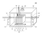
- the quantum converter 200 according to the second embodiment has a stack 20 instead of the stack 10.
- the laminate 20 includes a plurality of topological insulator films 11 and a plurality of ferromagnetic films 12 stacked on top of each other.
- the topological insulator films 11 and the ferromagnetic films 12 are stacked alternately.
- the laminate 10 has a plurality of interfaces 13.
- the second embodiment can also provide a high conversion efficiency.
- the stack 10 includes a plurality of topological insulator films 11 and a plurality of interfaces 13, so that a higher conversion efficiency ⁇ TI can be obtained.
- the conversion efficiency ⁇ TI of the stack 20 in the second embodiment is about 10 4 times larger than the conversion efficiency ⁇ YIG of the sphere 10Y in the second reference example.
- FIG. 5 is a diagram showing the relationship between the thickness d of the ferromagnetic film 12, the number N L of the topological insulator films 11, and the conversion efficiency ratio ( ⁇ TI / ⁇ YIG ). As shown in FIG. 5, if the number N L of the topological insulator films 11 is constant, the smaller the thickness d of the topological insulator film 11, the larger the conversion efficiency ratio ( ⁇ TI / ⁇ YIG ).
- the thickness d of the topological insulator film 11 is constant, the larger the number N L of the topological insulator films 11, the larger the conversion efficiency ratio ( ⁇ TI / ⁇ YIG ).
- the thickness of the ferromagnetic film 12 is preferably 1 nm or more and 20 nm or less.
- the quantum converter 300 according to the third embodiment has a stack 21 instead of the stack 20.
- the stack 21 includes a plurality of topological insulator films 11, a plurality of ferromagnetic films 12, and a plurality of nonmagnetic spacers 14, which are stacked on top of each other.
- the topological insulator films 11 and the spacers 14 are alternately stacked, and the ferromagnetic film 12 is disposed between the topological insulator films 11 and the spacers 14.
- the spacers 14 include, for example, Si, SrTiO 3 , InP, or Al 2 O 3 , or any combination thereof.
- the spacers 14 may be a Si film, a SrTiO 3 film, an InP film, or an Al 2 O 3 film.
- the distance between two adjacent topological insulator films 11 in the stacking direction is, for example, 5 nm or more.
- the thickness of the spacer 14 is, for example, 3 nm or more. If the thickness of the spacer 14 is 3 nm or more and the thickness of the ferromagnetic film 12 is 1 nm or more, the distance between two adjacent topological insulator films 11 in the stacking direction will be 5 nm or more. If the distance between two adjacent topological insulator films 11 in the stacking direction is less than 5 nm, there is a risk of hybridization of the surface state between these two topological insulator films 11. If the distance between two adjacent topological insulator films 11 in the stacking direction is 5 nm or more, this hybridization can be suppressed.
- the fourth embodiment differs from the second embodiment mainly in the polarization of the laser light irradiated onto the stack.
- Fig. 7 is a schematic diagram showing a quantum converter according to the fourth embodiment.
- laser light L3 is irradiated from the outside toward the stack 20 through the inlet 31.
- the laser light L3 includes two types of laser light whose deflection angles are orthogonal to each other.
- the laser light L3 is irradiated onto the first surface of the stack 20.
- the outlet 32 does not necessarily have to be provided.
- microwaves corresponding to the polarization of the laser light L3 are emitted from the laminate 20 and output to the outside through the antenna 40.
- the optical photons of the laser light L3 irradiated to the laminate 10 are quantum converted into microwave photons of microwaves.
- the fourth embodiment also provides high conversion efficiency, similar to the second embodiment.
- laminate 10 or 21 may be used instead of laminate 20.
- the quantum converter according to the present disclosure can be used, for example, for communication between superconducting quantum bits housed in each of a number of refrigerators.
- the use of the quantum converter according to the present disclosure is not limited to communication between superconducting quantum bits.
- the quantum converter can be used for quantum computing.
- Topological insulator film 12 Ferromagnetic film 13: Interface 14: Spacer 15: Substrate 30: Microwave resonator 31: Inlet 32: Outlet 40: Antenna 51: South pole 52: North pole 100, 200, 300, 400: Quantum converter
Landscapes
- Physics & Mathematics (AREA)
- General Physics & Mathematics (AREA)
- Engineering & Computer Science (AREA)
- Theoretical Computer Science (AREA)
- Mathematical Analysis (AREA)
- Condensed Matter Physics & Semiconductors (AREA)
- Data Mining & Analysis (AREA)
- Evolutionary Computation (AREA)
- Computational Mathematics (AREA)
- Mathematical Optimization (AREA)
- Pure & Applied Mathematics (AREA)
- Computing Systems (AREA)
- General Engineering & Computer Science (AREA)
- Mathematical Physics (AREA)
- Software Systems (AREA)
- Artificial Intelligence (AREA)
- Thin Magnetic Films (AREA)
Priority Applications (2)
| Application Number | Priority Date | Filing Date | Title |
|---|---|---|---|
| JP2025530849A JPWO2025009053A1 (https=) | 2023-07-04 | 2023-07-04 | |
| PCT/JP2023/024748 WO2025009053A1 (ja) | 2023-07-04 | 2023-07-04 | 量子変換器及び量子変換方法 |
Applications Claiming Priority (1)
| Application Number | Priority Date | Filing Date | Title |
|---|---|---|---|
| PCT/JP2023/024748 WO2025009053A1 (ja) | 2023-07-04 | 2023-07-04 | 量子変換器及び量子変換方法 |
Publications (1)
| Publication Number | Publication Date |
|---|---|
| WO2025009053A1 true WO2025009053A1 (ja) | 2025-01-09 |
Family
ID=94171636
Family Applications (1)
| Application Number | Title | Priority Date | Filing Date |
|---|---|---|---|
| PCT/JP2023/024748 Ceased WO2025009053A1 (ja) | 2023-07-04 | 2023-07-04 | 量子変換器及び量子変換方法 |
Country Status (2)
| Country | Link |
|---|---|
| JP (1) | JPWO2025009053A1 (https=) |
| WO (1) | WO2025009053A1 (https=) |
Citations (3)
| Publication number | Priority date | Publication date | Assignee | Title |
|---|---|---|---|---|
| JP2013500530A (ja) | 2009-09-21 | 2013-01-07 | インターナショナル・ビジネス・マシーンズ・コーポレーション | ハイブリッド超伝導体−光量子中継器、これを用いる方法およびシステム |
| JP2019512104A (ja) | 2016-02-08 | 2019-05-09 | インターナショナル・ビジネス・マシーンズ・コーポレーションInternational Business Machines Corporation | 歪み誘導型電気光学材料を有する集積マイクロ波−光単一フォトントランスデューサ |
| US20220215281A1 (en) | 2020-12-08 | 2022-07-07 | Dirk Robert Englund | Optically Heralded Entanglement of Superconducting Systems in Quantum Networks |
-
2023
- 2023-07-04 JP JP2025530849A patent/JPWO2025009053A1/ja active Pending
- 2023-07-04 WO PCT/JP2023/024748 patent/WO2025009053A1/ja not_active Ceased
Patent Citations (3)
| Publication number | Priority date | Publication date | Assignee | Title |
|---|---|---|---|---|
| JP2013500530A (ja) | 2009-09-21 | 2013-01-07 | インターナショナル・ビジネス・マシーンズ・コーポレーション | ハイブリッド超伝導体−光量子中継器、これを用いる方法およびシステム |
| JP2019512104A (ja) | 2016-02-08 | 2019-05-09 | インターナショナル・ビジネス・マシーンズ・コーポレーションInternational Business Machines Corporation | 歪み誘導型電気光学材料を有する集積マイクロ波−光単一フォトントランスデューサ |
| US20220215281A1 (en) | 2020-12-08 | 2022-07-07 | Dirk Robert Englund | Optically Heralded Entanglement of Superconducting Systems in Quantum Networks |
Non-Patent Citations (6)
| Title |
|---|
| J. MACIEJKO ET AL., PHYS., vol. 105, 2010, pages 166803 |
| R. HISATOMI ET AL., PHYS., vol. 93, 2016, pages 174427 |
| ROCHMAN JAKE, XIE TIAN, BARTHOLOMEW JOHN G., SCHWAB K. C., FARAON ANDREI: "Microwave-to-optical transduction with erbium ions coupled to planar photonic and superconducting resonators", NATURE COMMUNICATIONS, NATURE PUBLISHING GROUP, UK, vol. 14, no. 1, UK, XP093258260, ISSN: 2041-1723, DOI: 10.1038/s41467-023-36799-0 * |
| TSEMACDONALD, PHYS. REV., vol. 105, 2010, pages 057401 |
| WANG-KONG TSE; A. H. MACDONALD: "Giant Magneto-optical Kerr Effect and Universal Faraday Effect in Thin-film Topological Insulators", ARXIV.ORG, CORNELL UNIVERSITY LIBRARY, 201 OLIN LIBRARY CORNELL UNIVERSITY ITHACA, NY 14853, 11 March 2010 (2010-03-11), 201 Olin Library Cornell University Ithaca, NY 14853 , XP080395189, DOI: 10.1103/PhysRevLett.105.057401 * |
| XU YUNTAO, SAYEM AYED AL, FAN LINRAN, ZOU CHANG-LING, WANG SIHAO, CHENG RISHENG, FU WEI, YANG LIKAI, XU MINGRUI, TANG HONG X.: "Bidirectional interconversion of microwave and light with thin-film lithium niobate", NATURE COMMUNICATIONS, NATURE PUBLISHING GROUP, UK, vol. 12, no. 1, UK, XP093258264, ISSN: 2041-1723, DOI: 10.1038/s41467-021-24809-y * |
Also Published As
| Publication number | Publication date |
|---|---|
| JPWO2025009053A1 (https=) | 2025-01-09 |
Similar Documents
| Publication | Publication Date | Title |
|---|---|---|
| Cai et al. | Superconductor/ferromagnet heterostructures: A platform for superconducting spintronics and quantum computation | |
| Li et al. | Hybrid magnonics: Physics, circuits, and applications for coherent information processing | |
| Zhu et al. | Magnon-photon strong coupling for tunable microwave circulators | |
| Kutsaev et al. | Up‐and‐coming advances in optical and microwave nonreciprocity: From classical to quantum realm | |
| Platzman et al. | Magnetic scattering of x rays from electrons in molecules and solids | |
| Zheng et al. | High‐Efficiency Magnon‐Mediated Magnetization Switching in All‐Oxide Heterostructures with Perpendicular Magnetic Anisotropy | |
| CN109583592B (zh) | 多超导量子比特中任意两个比特耦合的方法及其系统 | |
| US9767876B2 (en) | Magnonic holographic memory and methods | |
| JP3834616B2 (ja) | スピンフィルタ | |
| Haldar et al. | Functional magnetic waveguides for magnonics | |
| EA003164B1 (ru) | Квантово-размерные электронные устройства и режимы их работы | |
| Dionne et al. | Circular polarization and nonreciprocal propagation in magnetic media | |
| Mandal | Transmission and conductance across junctions of isotropic and anisotropic three-dimensional semimetals | |
| Zheng et al. | Double-barrier magnetic tunnel junctions with enhanced tunnel magnetoresistance | |
| Wei et al. | Heralded Universal Quantum Gate and Entangler Assisted by Imperfect Double‐Sided Quantum‐Dot‐Microcavity Systems | |
| Sharma et al. | Shunt-free cryogenic memory using ferromagnetic insulator-based Josephson junctions | |
| WO2024150293A1 (ja) | 量子変換器及び量子変換方法 | |
| Mayr et al. | Time-resolved x-ray imaging of nanoscale spin-wave dynamics at multi-GHz frequencies using low-alpha synchrotron operation | |
| WO2025009053A1 (ja) | 量子変換器及び量子変換方法 | |
| Lian et al. | Tunable Chern Number and Sizable Bandgap in Kagome‐Honeycomb‐Triangle Latticed Quantum Anomalous Hall Insulator | |
| Taravati | Light transmission through space-time-modulated josephson junction arrays and application to quantum angular-frequency beam multiplexing | |
| Vilela et al. | Thermally driven magnon valve with perpendicular magnetic anisotropy | |
| JP2018206855A (ja) | 積層構造体及びスピン変調素子 | |
| Ohno et al. | Room-temperature spin relaxation in a (110)-oriented GaAs/AlGaAs superlattice with tunnel-coupled quantum wells | |
| JPH01319021A (ja) | 光学素子 |
Legal Events
| Date | Code | Title | Description |
|---|---|---|---|
| 121 | Ep: the epo has been informed by wipo that ep was designated in this application |
Ref document number: 23944305 Country of ref document: EP Kind code of ref document: A1 |
|
| ENP | Entry into the national phase |
Ref document number: 2025530849 Country of ref document: JP Kind code of ref document: A |
|
| WWE | Wipo information: entry into national phase |
Ref document number: 2025530849 Country of ref document: JP |
|
| WWE | Wipo information: entry into national phase |
Ref document number: 2023944305 Country of ref document: EP |
|
| NENP | Non-entry into the national phase |
Ref country code: DE |
|
| ENP | Entry into the national phase |
Ref document number: 2023944305 Country of ref document: EP Effective date: 20260204 |