WO2025005104A1 - 波長変換素子、これを用いた光回路、及び光源装置 - Google Patents
波長変換素子、これを用いた光回路、及び光源装置 Download PDFInfo
- Publication number
- WO2025005104A1 WO2025005104A1 PCT/JP2024/023094 JP2024023094W WO2025005104A1 WO 2025005104 A1 WO2025005104 A1 WO 2025005104A1 JP 2024023094 W JP2024023094 W JP 2024023094W WO 2025005104 A1 WO2025005104 A1 WO 2025005104A1
- Authority
- WO
- WIPO (PCT)
- Prior art keywords
- polar member
- polar
- wavelength conversion
- conversion element
- core
- Prior art date
- Legal status (The legal status is an assumption and is not a legal conclusion. Google has not performed a legal analysis and makes no representation as to the accuracy of the status listed.)
- Ceased
Links
Images









Classifications
-
- G—PHYSICS
- G02—OPTICS
- G02F—OPTICAL DEVICES OR ARRANGEMENTS FOR THE CONTROL OF LIGHT BY MODIFICATION OF THE OPTICAL PROPERTIES OF THE MEDIA OF THE ELEMENTS INVOLVED THEREIN; NON-LINEAR OPTICS; FREQUENCY-CHANGING OF LIGHT; OPTICAL LOGIC ELEMENTS; OPTICAL ANALOGUE/DIGITAL CONVERTERS
- G02F1/00—Devices or arrangements for the control of the intensity, colour, phase, polarisation or direction of light arriving from an independent light source, e.g. switching, gating or modulating; Non-linear optics
- G02F1/35—Non-linear optics
- G02F1/37—Non-linear optics for second-harmonic generation
- G02F1/377—Non-linear optics for second-harmonic generation in an optical waveguide structure
Definitions
- This disclosure relates to a wavelength conversion element, an optical circuit using the same, and a light source device.
- Second-order nonlinear optical effects include sum frequency generation and difference frequency generation, and are used in second harmonic generation (SHG) and optical parametric amplification. Wavelength conversion is also performed using these nonlinear optical effects.
- Wavelength conversion waveguides consisting of periodically inverted polarization of ferroelectrics such as lithium niobate (LN) and lithium tantalate (LT) are commonly known as wavelength converters, but they are difficult to microfabricate and have a low damage threshold in the visible light band.
- a method has been proposed in which GaN layers are grown in opposing directions from the side walls of a groove formed in a substrate, and a waveguide element for wavelength conversion is fabricated using a first crystal region and a second crystal region with c-axes in opposite directions (see, for example, Patent Document 1). Also, a quasi-phase-matched waveguide has been proposed in which an AlN thin film having a second-order nonlinear optical constant and HfO2 having no polarization are laminated in this order on the surface of a substrate (see, for example, Non-Patent Documents 1 and 2).
- the method of growing a GaN layer with a c-axis in the opposite direction in the groove involves a complicated manufacturing process, and the quality of the crystal near the interface with the substrate is insufficient.
- the thickness of the AlN thin film is small, making it difficult to grow a high-quality crystal thin film.
- a wavelength conversion element is provided that can utilize a high-quality crystal portion with a simple configuration.
- the wavelength converting element comprises: A substrate having a major surface; an optical waveguide disposed on the main surface of the substrate; Equipped with a core of the optical waveguide includes a polar member having a second-order nonlinear optical constant and a first nonpolar member disposed adjacent to the polar member in a direction parallel to the main surface of the substrate; In a cross section perpendicular to the optical axis of the optical waveguide, one or both side surfaces of the polar member are in contact with the first non-polar member.
- a wavelength conversion element that can utilize high-quality crystal parts with a simple configuration has been realized.
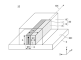
- FIG. 1 is a schematic perspective view of a wavelength conversion element according to a first embodiment.
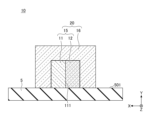
- FIG. 2 is a cross-sectional view perpendicular to the optical axis of FIG. 1 .
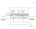
- 1A and 1B are diagrams illustrating a waveguide mode propagating through an optical waveguide of a wavelength conversion element.
- FIG. 13 is a schematic diagram of a first modified example of a wavelength conversion element.
- 5A to 5C are diagrams showing the steps of manufacturing the optical waveguide of the wavelength conversion element of FIG. 4.
- 5A to 5C are diagrams showing the steps of manufacturing the optical waveguide of the wavelength conversion element of FIG. 4.
- 5A to 5C are diagrams showing the steps of manufacturing the optical waveguide of the wavelength conversion element of FIG. 4.
- FIG. 13 is a schematic diagram of a second modified example of the wavelength conversion element.
- FIG. 13 is a schematic diagram of a third modified example of the wavelength conversion element.
- FIG. 13 is a schematic diagram of yet another modified example of the wavelength conversion element.
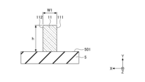
- FIG. 13 is a model diagram for calculating the core width for phase matching.
- FIG. 1 is a diagram showing an electromagnetic field distribution of the TM 00 mode of an optical waveguide.
- FIG. 13 is a diagram showing the electromagnetic field distribution of the TM 20 mode of the optical waveguide.
- FIG. 13 is a diagram showing the calculation results of the core width for phase matching in a transverse mode.
- FIG. 5 is a cross-sectional view of a wavelength conversion element according to a second embodiment.
- FIG. 11 is a cross-sectional view of a wavelength conversion element according to a third embodiment.
- 13A and 13B are schematic diagrams of light propagating through a wavelength conversion element according to a third embodiment.
- FIG. 13 is a cross-sectional view of a wavelength conversion element according to a fourth embodiment.
- FIG. 13 is a cross-sectional view of a wavelength conversion element according to a modified example of the fourth embodiment.
- FIG. 13 is a cross-sectional view of a wavelength conversion element according to a fifth embodiment.
- FIG. 13 is a cross-sectional view of a wavelength conversion element according to a modified example of the fifth embodiment.
- 1 is a schematic diagram of a light source device using a wavelength conversion element according to an embodiment.
- 1 is a schematic diagram of an optical circuit using a wavelength conversion element according to an embodiment.
- the wavelength conversion element of the embodiment can be used for purposes other than SHG.
- it is possible to perform wavelength conversion in the reverse process of SHG i.e., conversion from angular frequency ⁇ 2 to angular frequency ⁇ 1 ).
- It can also be used as a wavelength conversion element that performs arbitrary wavelength conversion by sum frequency generation or difference frequency generation within a range that satisfies the phase matching condition described later.
- the guided mode In optical waveguides, the guided mode cannot strictly be separated into TM mode and TE mode, and contains components of both. This is called TM-like mode or TE-like mode. In the specification, for the sake of simplicity, it is referred to simply as TM mode, but this stands for TM-like mode.
- Fig. 1 is a schematic perspective view of a wavelength conversion element 10 of the first embodiment
- Fig. 2 is a cross-sectional view perpendicular to the optical axis OX of Fig. 1.
- the direction parallel to the optical axis OX of the wavelength conversion element 10 is defined as the Z direction
- the normal direction to the surface of the substrate 5 in the XY plane perpendicular to the optical axis OX is defined as the Y direction.
- the wavelength conversion element 10 comprises a substrate 5 having a principal surface 501, and an optical waveguide 20 disposed on the principal surface 501 of the substrate 5.
- the core 15 of the optical waveguide 20 includes a polar member 11 having a second-order nonlinear optical constant, and a first nonpolar member 12 disposed adjacent to the polar member 11 in the X direction parallel to the principal surface 501 of the substrate 5.
- XY plane which is a cross section perpendicular to the optical axis OX of the optical waveguide 20
- one or both side surfaces 111 of the polar member 11 and the first nonpolar member 12 are in contact. This allows a region with relatively high crystal quality to be used as a waveguide path, thereby reducing optical loss due to the waveguide itself.
- the "direction parallel to" the main surface 501 does not require that the main surface 501 and the X-axis be strictly parallel in the XY plane, but may include manufacturing errors and process errors, and may include a deviation of, for example, ⁇ 2° or less, preferably ⁇ 0.1° or less.
- one side surface 111 of the polar member 11 is disposed in contact with the first non-polar member 12, but as described below, the first non-polar member 12 may be disposed in contact with both side surfaces of the polar member 11.
- the side surface 111 does not need to be perpendicular to the main surface 501 of the substrate 5, and the shape of the polar member 11 in the XY cross section may be a trapezoid or an inverted trapezoid.
- the core 15 of the optical waveguide 20 is composed of the polar member 11 and the first non-polar member 12 that are in contact with each other in the lateral direction (X direction) on the main surface 501 of the substrate 5.
- the polar member 11 is formed of, for example, a wurtzite crystal having polarization in the c-axis direction.
- the polar member 11 can receive light with a higher power density than LN or LT, thereby increasing the conversion efficiency of the wavelength conversion element 10.
- the c-axis of the polar member 11 formed on the substrate 5 is perpendicular to 501 of the substrate 5, and has polarization in the direction of the arrow.
- AlN, GaN, ZnO, etc., represented by the general formula AB have a wurtzite crystal structure.
- the polar member 11 is formed of Al x Ga 1-x N (0 ⁇ x ⁇ 1). By adjusting the value of x, the difference in refractive index with the first non-polar member 12 can be reduced.
- the first non-polar member 12 is a material having no polarity.
- the first non-polar member 12 is preferably formed as an amorphous layer.
- the first non-polar member 12 may be selected from the group consisting of Nb 2 O 5 , Ta 2 O 5 , TiO 2 , HfO 2 , ZrO 2 , and Si 3 N 4.
- the composition does not necessarily have to match the stoichiometry, and may be in a state in which oxygen or nitrogen is more or less than the stoichiometry.
- the first non-polar member 12 may be a composite material containing two or more of the above materials. Alternatively, the refractive index may be adjusted by doping with an impurity.
- This modulation reduces the cancellation of the coupling constant ⁇ , which will be described later, caused by the positive and negative antinodes of the amplitude of the high-order lateral mode generated in the core 15.
- the spatial modulation here refers to modulation due to the presence or absence of a second-order nonlinear optical constant, and contributes to the efficiency of wavelength conversion.
- the core 15 formed of the polar member 11 and the first non-polar member 12 is surrounded by the cladding 16.
- the cladding 16 preferably covers both the side and top surfaces of the core 15.
- the cladding 16 surrounding the core 15 may be an air layer, or a layer of a material having a lower refractive index than the core 15 may be provided. Silicon oxide (SiO 2 ), silicon oxynitride (SiON), aluminum oxide (Al 2 O 3 ), aluminum oxynitride (AlON), etc. may be used as a material having a lower refractive index than the core 15.
- the refractive index of the cladding is one of the parameters that determine the modal dispersion and is set appropriately.
- the height h of the core 15 in the XY cross section corresponds to the film thickness of the polar member 11 and the first non-polar member 12.
- the height h of the core has a sufficient thickness to increase the confinement of light, and is, for example, 300 nm to 1 ⁇ m.
- the width W of the core 15 is the sum of the width W1 of the polar member 11 and the width W2 of the first non-polar member 12. In the embodiment, the width W of the core 15 relative to the width W1 of the polar member 11 is set so that the TM 00 mode of the fundamental wave and the TM 20 mode of the second harmonic wave satisfy the phase matching condition. The phase matching condition will be described later.
- the height h of the polar member 11 may be equal to or greater than the width W1.
- the aspect ratio (h/W) of the height h and width W of the core 15 may be, for example, 1 to 5, preferably 1 to 3.
- the aspect ratio (h/W1) of the height h and width W1 of the polar member may be, for example, 2 to 10, preferably 2 to 6.
- the aspect ratio (h/W2) of the height h to the width W2 of the first non-polar member 12 may be, for example, 2 to 10, and preferably 2 to 6.
- the width W1 of the polar member 11 may be 0.5 to 2 times the width W2 of the first non-polar member 12.
- the magnitude of the polarization of the polar member 11 is proportional to the magnitude of the optical electric field.
- the polarization of the polar member 11 exhibits second-order and/or third-order nonlinear polarization.
- the effect resulting from such nonlinear polarization is the nonlinear optical effect.
- SHG is a representative second-order nonlinear optical effect.
- FIG. 3 is a schematic diagram of a guided mode propagating through the optical waveguide 20.
- the intensity distribution of the pump light and the signal light in the XY cross section is shown as being integrated in the Y direction and projected onto the XZ plane.
- the pump light in the TM 00 mode with an angular frequency of ⁇ 1 is incident on the wavelength conversion element 10 in the Z direction.
- the incidence of the pump light induces nonlinear polarization in the polar member 11 of the core 15, and a signal light with an angular frequency ⁇ 2 different from ⁇ 1 is generated.
- ⁇ 2 is, for example, twice the angular frequency of ⁇ 1.
- the guided mode of the signal light with an angular frequency ⁇ 2 is the TM 20 mode.
- the polar member 11 of the core 15 has a second-order nonlinear optical constant d.
- the second-order nonlinear optical constant is a third-order tensor, and when the energy of light input and output to the polar member 11 is sufficiently smaller than the band gap energy of the polar member 11, it is expressed by d ij, which is a component of a 3 ⁇ 6 matrix, using a contracted expression.
- the second-order nonlinear optical constant d ij is proportional to the second-order nonlinear susceptibility ⁇ (2) .
- the second-order nonlinear optical constant has different components that take finite values depending on the symmetry of the crystal that constitutes the polar member 11.
- the polar member 11 has, for example, a second-order nonlinear optical constant d 33.
- d 33 can be used as the maximum component.
- the signal light of angular frequency ⁇ 2 generated by the interaction between the incident pump light and the polar member 11 propagates through the optical waveguide 20 in the TM 20 mode and is output from the wavelength conversion element 10.
- the second-order nonlinear optical constant is not limited to d 33 . Taking into consideration the direction of the polarity and the direction of the optical electric field incident on the polar member 11, other components such as d31 may be used.
- phase matching condition between the pump light and the signal light in order to efficiently generate a second harmonic wave by utilizing the second-order nonlinear optical effect, it is necessary to satisfy the phase matching condition between the pump light and the signal light.
- the refractive index depends on the angular frequency, it is difficult to achieve phase matching in two states of angular frequency, ⁇ 1 and ⁇ 2.
- phase matching using a transverse mode is used.
- the refractive index of the material of the core 15 felt by the light of the wavelength of the pump light i.e., the light of the angular frequency ⁇ 1
- the refractive index of the material of the core 15 felt by the light of the wavelength of the signal light i.e., the light of the angular frequency ⁇ 2
- the band gap energy of the wavelength conversion element 10 is sufficiently larger than the energy of the pump light and the signal light
- the refractive index of the core material felt by the light of the short wavelength is larger than that of the light of the long wavelength, n mat ( ⁇ 1 ) ⁇ n mat ( ⁇ 2 )
- the effective refractive index n 00 of the core 15 in the fundamental mode is larger than the effective refractive index n m0 in the higher-order transverse mode, n00 > nm0
- n 00 ( ⁇ 1 ) n m0 ( ⁇ 2 ) That is, the pump light and the signal light in the core 15 can satisfy the phase matching condition.
- the coupling constant ⁇ is proportional to the value obtained by multiplying the second-order nonlinear susceptibility ⁇ (2) by the square of the electric field E ⁇ 1 and the electric field E ⁇ 2 and integrating the result over the core cross section.
- the second-order nonlinear susceptibility ⁇ (2) is zero in the region of the first nonpolar member 12.
- the first non-polar member 12 by designing the first non-polar member 12 to include one positive and one negative antinode in the electric field distribution of the TM 20 mode, only the remaining antinodes contribute to the coupling constant ⁇ . This makes it possible to increase the coupling constant ⁇ compared to the case where phase matching is achieved with a core made of only polar members.
- the coupling constant ⁇ of the core 15 depends on the overlap of the electric fields of the TM 00 mode and the TM 20 mode in the cross-sectional area of the core 15. For example, by designing the optical waveguide 20 so that the interface between the polar member 11 and the first non-polar member 12 is located at a node of the amplitude of the signal light of the TM 20 mode, the cancellation of positive and negative signals in the overlap of the TM 00 mode and the TM 20 mode in the polar member 11 is reduced. This allows the coupling constant ⁇ to be increased compared to a configuration in which cancellation of positive and negative antinodes of a higher mode occurs when the core 15 is formed only with the polar member 11.
- the transverse mode in the Y direction in FIG. 3 is preferably the fundamental mode. This allows efficient wavelength conversion by increasing the coupling constant ⁇ .
- FIG. 4 is a schematic diagram of a wavelength conversion element 10A as a first modified example of the wavelength conversion element 10.
- the wavelength conversion element 10A has an optical waveguide 20A on the main surface 501 of the substrate 5.
- the optical waveguide 20A includes a core 15A and a clad 16.
- the core 15A has a polar member 11 and a first non-polar member 12 arranged in contact with the side surfaces 111 and 112 on both sides of the polar member 11.
- the polar member 11 is sandwiched between the first non-polar member 12.
- the wavelength conversion element 10A has a simple configuration.
- the polar member 11 and the first non-polar member 12 can be formed thick in the Y direction, and the crystal quality can be improved.
- a polar material can be arranged in the region where the electric field strength of each of the TM 00 mode and the TM 20 mode is high.
- the electric field distribution of the TM 20 mode has three antinodes.
- the coupling constant ⁇ in the formula 1 can be increased by setting the width of the core 15A so that the polar member 11 includes at least the central antinode and the two first non-polar members 12 include the vertices of the outer antinodes. Therefore, the wavelength conversion can be performed efficiently.
- the width W1 of the polar member 11 may be, for example, 0.5 to 3 times, preferably 1 to 2 times, the sum (W-W1) of the widths W2 of the two first non-polar members 12.
- the aspect ratio (h/W) of the height h and width W of the core 15 may be, for example, 0.5 to 10, preferably 0.5 to 6.
- ⁇ Process for Producing Core 15A> 5A to 5D are diagrams showing the steps of manufacturing the core 15A of the wavelength conversion element 10A.
- a layer 110 of polar material is formed on the main surface 501 of the substrate 5.
- the substrate 5 can be selected from a suitable substrate such as a sapphire substrate, a GaN substrate, a quartz substrate, an optical glass substrate, a resin substrate, and a silicon substrate with a silicon oxide film.
- the substrate 5 is preferably a sapphire substrate or a GaN substrate.
- the layer 110 of polar material can be formed with relatively high quality.
- As the polar material a material having a wurtzite crystal structure such as AlN, GaN, AlGaN, or ZnO is used.
- a layer 110 of polar material with good crystal quality is formed by physical vapor deposition (PVD) such as sputtering and evaporation, or chemical vapor deposition (CVD).
- PVD physical vapor deposition
- CVD chemical vapor deposition
- the composition of Al and Ga may be adjusted to obtain a desired refractive index.
- the thickness of the layer 110 of polar material is, for example, 300 nm to 1000 nm. Since the phase matching condition can be satisfied by controlling the transverse mode in the width direction (X direction) of the core, the layer 110 of polar material can be made relatively thick. This can improve the crystal quality of the layer 110 of polar material.
- the layer 110 is processed into a predetermined shape to obtain the polar member 11.
- the polar member 11 is obtained by processing the layer 110 through a mask patterned into a predetermined shape.
- the predetermined shape is a shape extending in the Z direction with a width W1 and a height h in the XY cross section as shown in FIG. 1.
- the height h may be greater than or equal to the width W1.
- the aspect ratio (h/W1) of the height h and the width W1 may be 1 to 10, preferably 1.5 to 6.
- the shape of the XY cross section does not necessarily have to be rectangular, and may be a trapezoid, an inverted trapezoid, or the like.
- the side surfaces 111 and 112 that form a predetermined angle with the main surface 501 of the substrate 5 are obtained.
- the anisotropic etching may be, for example, a dry process or reactive ion etching.
- the polar member 11 is a material suitable for microfabrication and can be processed into a predetermined width.
- a layer 120 of a non-polar material is formed on the entire surface, covering the polar member 11.
- the layer 120 of the non-polar material is an amorphous layer that does not have polarization.
- a material having a refractive index relatively close to that of the polar member 11 is used.
- the difference between the refractive index of the polar member 11 and the refractive index of the layer 120 of the non-polar material may be, for example, 0.001 to 0.2, or 0.001 to 0.1.
- the non-polar material is selected from the group consisting of Nb 2 O 5 , Ta 2 O 5 , TiO 2 , HfO 2 , ZrO 2 , and Si 3 N 4.
- the composition does not necessarily have to match the stoichiometry, and may be in a state where oxygen or nitrogen is more or less than the stoichiometry.
- the layer 120 of the non-polar material may be a layer of a composite material containing two or more of the above materials.
- the refractive index may be adjusted by doping impurities. This can reduce the difference between the refractive index of the non-polar material layer 120 and the refractive index of the polar member 11, and therefore can increase the number of combinations of angular frequencies that achieve phase matching between light with angular frequency ⁇ 1 and light with angular frequency ⁇ 2 .
- the non-polar material layer 120 may be made of Nb2O5 or TiO2 .
- the polar member 11 is made of AlN , Ta2O5 , HfO2 , Si3N4 , or the like may be used.
- the amorphous non-polar material layer 120 is formed by a PVD method, a CVD method, an atomic layer deposition (ALD) method, or the like. By using the CVD method or the ALD method, the non-polar material layer 120 with good coverage can be formed on the side surfaces 111 and 112 of the polar member 11.
- the layer 120 of non-polar material is processed by anisotropic etching to form a first non-polar member 12 that contacts both side surfaces 111 and 112 of the polar member 11.
- the core 15A with good crystal quality in the portion away from the substrate 5 is obtained.
- the steps from FIG. 5A to 5D can be realized by a wafer process suitable for mass production, and a core 15A with a simple configuration can be manufactured by a simple process.
- a cladding 16 may be further formed.
- the cladding 16 may be air.
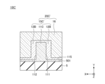
- FIG. 6A is a schematic diagram of a wavelength conversion element 10B of a second modified example of the wavelength conversion element 10.
- the optical waveguide 20B of the wavelength conversion element 10B has a core 15B composed of a polar member 11 and a first non-polar member 12B.
- the first non-polar member 12B is in contact with the side surfaces 111 and 112 on both sides of the polar member 11 and the upper surface.
- the end time of the anisotropic etching is controlled to obtain the core 15B in the shape of FIG. 6A.
- a thin film 121 of the non-polar material remains on the main surface 501 of the substrate 5.
- the core 15B in the shape of FIG. 6A is advantageous in that the film thickness of the polar member 11 can be maintained without overcutting the polar member 11.
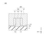
- FIG. 6B is a schematic diagram of a wavelength conversion element 10C of a third modified example of the wavelength conversion element 10.
- the optical waveguide 20C of the wavelength conversion element 10C has a core 15C composed of a polar member 11C and a first non-polar member 12 on the main surface 501 of the substrate 5.
- the first non-polar member 12B is in contact with the side surfaces 111 and 112 on both sides of the polar member 11 and the upper surface.
- the core 15C having the shape of FIG. 6B is obtained by controlling the end time of the anisotropic etching of the polar material layer 110.
- the core 15C having the shape of FIG. 6B is also advantageous in that the film thickness can be secured without excessively removing the polar member 11.
- FIG. 6C is a schematic diagram showing yet another modified example of the wavelength conversion element 10.
- the configuration of FIG. 6A and the configuration of FIG. 6B may be combined to form the configuration of the wavelength conversion element 10C'.
- the optical waveguide 20C' has a core 15C' composed of a polar member 11C and a first non-polar member 12B on the main surface 501 of the substrate 5.
- the first non-polar member 12B is provided to cover the thin film 115 of the polar material and the upper surface of the polar member 11C, and the clad 16 is formed to cover the core 15C'. Even in the configuration of FIG. 6C, the film thickness can be ensured without excessively removing the polar member 11C.
- FIG. 7 is a model diagram for determining the core width that satisfies the phase matching condition.
- the core shape in FIG. 4 is adopted as the model.
- the substrate 5 is sapphire
- the polar member 11 of the core 15 is AlN
- the first non-polar member 12 sandwiching both sides of the polar member 11 is Ta 2 O 5
- the clad 16 covering the core 15 is Al 2 O 3 .
- This allows the width and height of the core, the refractive index of the core, the refractive index of the clad, and the refractive index of the substrate to be defined. From this information, the electromagnetic field distribution and the effective refractive index can be obtained by the finite element method.
- the height h of the core 15 is fixed at 400 nm, the width W of the polar member 11 is fixed at 300 nm, and the width W of the core 15 is changed by changing the width of the first non-polar member 12.
- the effective refractive index neff in the fundamental wave TM00 mode having a wavelength of 810 nm and the second harmonic wave TM20 mode having a wavelength of 405 nm are the same or sufficiently close to each other.
- the TM 00 mode with a wavelength of 810 nm shown in FIG. 8A is the guided mode of the pump light, which is the fundamental wave.
- the TM 20 mode with a wavelength of 405 nm shown in FIG. 8B is the TM 20 mode of the second harmonic.
- Three electric field loops are located in one polar member 11 and two first non-polar members 12, one each.
- FIG. 9 shows the calculation results of the effective refractive index n eff in the TM 00 mode and the TM 20 mode when the width W of the core 15 is changed while the width W1 of the polar member 11 is fixed at 300 nm.
- the open circles represent the calculation results of the dispersion curve in the transverse mode (TM mode) of the angular frequency ⁇ 1.
- the black circles represent the calculation results of the dispersion curve in the transverse mode (TM mode) of the angular frequency ⁇ 2.
- the width W of the core 15 is 550 nm
- the effective refractive index of the TM 00 mode of the angular frequency ⁇ 1 and the effective refractive index of the TM 20 mode of the angular frequency ⁇ 2 are the same.
- the width W1 of the polar member 11 is 300 nm
- the width W of the core 15 is set to 550 nm, so that the fundamental wave TM 00 mode (810 nm) and the second harmonic TM 20 mode (405 nm) can be phase-matched. That is, the 0th and 2nd order modes are used in the X direction, and the 0th order modes are phase-matched in the Y direction. This increases the coupling constant ⁇ , enabling efficient wavelength conversion.
- the dispersion curves indicated by black circles other than the dispersion curve of the second harmonic TM 20 (405 nm) are the TM m0 mode of the second harmonic (m is an integer of 0, 1, or 3 or more), and the existence of multiple higher-order modes is permitted when the width W of the core 15 is in the vicinity of 550 nm.
- the dispersion curves indicated by white circles other than the dispersion curve of the fundamental wave TM 00 (810 nm) are the higher-order modes of 810 nm (for example, the first-order mode), and the existence of higher-order modes is permitted when the width W of the core 15 is in the vicinity of 550 nm.
- FIG. 9 the dispersion curves indicated by black circles other than the dispersion curve of the second harmonic TM 20 (405 nm) are the TM m0 mode of the second harmonic (m is an integer of 0, 1, or 3 or more), and the existence of multiple higher-order modes is permitted when the width W of the core 15 is in the vicinity of
- the higher-order mode of 810 nm is not phase-matched with the TM 20 mode of 405 nm.
- the width W of the core 15 is wider and exceeds 800 nm, the higher-order mode of 810 nm appears.
- the fundamental wave TM 00 mode and the second harmonic TM 20 mode are not phase-matched.
- the width of the core 15 is a width in which the number of possible modes for the component of the first angular frequency (first frequency component) is three or less, and the number of possible modes for the harmonic component of the second angular frequency (second frequency component) that is greater than the first angular frequency is two or more.
- the width W of the core 15 may be 1.5 times or more and 4 times or less, preferably 1.75 times or more and 3.5 times or less, and more preferably 2 times or more and 3 times or less, the width W1 of the polar member 11. This improves the degree of freedom in the width of the optical waveguide that allows phase matching.
- the width W1 of the polar member 11 can be processed in the range of 100 nm to 1000 nm, and the width of the core 15 can be appropriately selected in the range of 200 nm to 2000 nm so that the fundamental wave TM 00 mode and the second harmonic wave TM 20 mode satisfy the transverse mode phase matching condition.
- the width W1 of the polar member 11 is in the range of 100 nm to 500 nm
- the width of the core 15 may be in the range of 200 nm to 1000 nm.
- FIG. 9 shows that if the angular frequency of the pump light, the angular frequency of the signal light, the refractive index of the core, and the refractive index of the cladding are determined, the core width that satisfies the phase matching condition can be obtained.
- the phase matching condition for SHG from 810 nm to 405 nm has been described, but the embodiment is not limited to this.
- the wavelength conversion may be an optical parametric process from 405 nm to 810 nm. Also, conversion to an arbitrary angular frequency may be performed by sum frequency generation or difference frequency generation.
- the phase matching is not limited to the TM 00 mode and the TM 20 mode, and both may be phase matched in a higher order mode.
- the TM p0 mode and the TM q0 mode (p and q are integers equal to or greater than 1) may be used.
- Second Embodiment 10 is a cross-sectional view of a wavelength conversion element 10D of the second embodiment.
- the wavelength conversion element 10D has an optical waveguide 20D disposed on the main surface 501 of the substrate 5.
- the core 15D of the optical waveguide 20D has a polar member 11 having a second-order nonlinear optical constant, a first nonpolar member 12 disposed adjacent to the polar member 11 in a direction parallel to the main surface 501 of the XY cross section (X direction), and a second nonpolar member 13 disposed outside the first nonpolar member 12 and in contact with the side surface of the first nonpolar member 12.
- the refractive index of the second nonpolar member 13 is greater than that of the first nonpolar member 12.
- the "outside" of the first nonpolar member 12 means the outside with the polar member 11 as the center when viewed in the X direction of the XY cross section. At this time, the first nonpolar member 12 is located between the polar member 11 and the second nonpolar member 13.
- the refractive index of the polar member 11 is n 1
- the refractive index of the first non-polar member 12 is n 2
- the refractive index of the second non-polar member 13 is n 3
- n 1 > n 3 > n 2 n 1
- GaN can be used for the polar member 11
- SiO 2 can be used for the first non-polar member 12
- Ta 2 O 5 can be used for the second non-polar member 13.
- the refractive index n mat of the material felt by the light of the pump light wavelength and the light of the signal light wavelength is n mat ( ⁇ 1 ) ⁇ n mat ( ⁇ 2 )
- the refractive index felt by the signal light of a short wavelength is high.
- the magnitude relationship of the effective refractive index in the TM 00 mode and the TM 20 mode is n 00 > n 20 , and the refractive index felt by the TM 00 mode is larger than the refractive index felt by the TM 20 mode.
- the optical density can be concentrated in the polar member 11, and phase matching can be achieved by utilizing the dispersion of the transverse mode.
- the signal light which is the second harmonic of the TM 20 mode, is confined to the first non-polar member 12 and the polar member 11 sandwiched between the first non-polar member 12, so that leakage out of the core 15D is reduced. Since one of the loops of the TM 20 mode can be concentrated in the polar member 11, the coupling constant ⁇ can be increased according to the formula 1, and wavelength conversion by nonlinear polarization can be efficiently performed.
- the refractive index of the second non-polar member 13 is visible, and the refractive index felt when propagating through the core 15 is high.
- the configuration of the second embodiment allows greater freedom in designing phase matching that utilizes transverse mode dispersion by selecting the refractive index of the material.
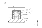
- FIG. 11 is an XY cross-sectional view of the wavelength conversion element 10E of the third embodiment.
- the wavelength conversion element 10E has an optical waveguide 20E arranged on the main surface 501 of the substrate 5.
- the core 15E of the optical waveguide 20E further has a third non-polar member 14 arranged on the upper surface of the polar member 11 and the upper surface of the first non-polar member 12.
- the refractive index of the third non-polar member 14 is equal to or greater than that of the polar member 11.
- the third non-polar member 14 having a refractive index equal to or greater than that of the polar member 11 allows light to be guided closer to the third non-polar member 14 than to the substrate 5.
- the light is concentrated more on the upper side of the core 15, which has a good crystalline state, to reduce loss and improve conversion efficiency.
- the crystal quality of the polar member 11 is better on the upper side of the core 15 than at the interface between the substrate 5 and the core 15.
- the refractive indexes of the polar member 11 and the first non-polar member 12 are approximately the same, and the refractive index of the third non-polar member 14 is equal to or higher than the refractive indexes of the polar member 11 and the first non-polar member 12.
- the light L including the pump light and the signal light is concentrated at the upper part of the core 15E, which has a large difference in refractive index with the cladding 16.
- the effective refractive index of the pump light in the TM 00 mode and the effective refractive index of the signal light in the TM 20 mode become equal, and the phase matching condition is satisfied.
- the configuration of the third embodiment can reduce losses and increase conversion efficiency by adjusting the refractive index distribution in the core 15.
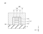
- Fourth Embodiment 13 is a cross-sectional view of a wavelength conversion element 10F of the fourth embodiment.
- the wavelength conversion element 10F has an optical waveguide 20F arranged on the main surface 501 of the substrate 5.
- the core 15F of the optical waveguide 20F has a polar member 11F and a first non-polar member 12 that contacts the polar member 11F on both side surfaces.
- the polar member 11F has a first polar member 116, a second polar member 117 and/or a third polar member 118 in the normal direction of the main surface 501 of the substrate 5.
- the first polar member 116 is arranged between the substrate 5 and the second polar member 117 or the third polar member 118.
- the refractive indexes of the second polar member 117 and the third polar member 118 are each greater than the refractive index of the first polar member 116. Only one of the second polar member 117 and the third polar member 118 may be used.
- the refractive indexes of the first polar member 116, the second polar member 117, and the third polar member 118 may be adjusted by adjusting the composition x of Al x Ga 1-x N (0 ⁇ x ⁇ 1).
- the first polar member 116 may be made of AlGaN
- the second polar member 117 or the third polar member 118 may be made of GaN.
- InGaN may be used for the polar member 11F.
- the configuration of the fourth embodiment also concentrates light on the upper side of the core 15F, which has a good crystal state, to reduce loss and improve conversion efficiency.
- the refractive index of the third polar member 118 may be larger than the refractive index of the first polar member 116 and the refractive index of the second polar member 117. This allows the light to be guided closer to the third polar member 118 than the substrate 5. Because the crystalline quality of the third polarity member 118 is higher than that of the first polarity member 116, light can be concentrated closer to the third polarity member 118 than to the first polarity member 116, reducing light loss.
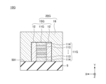
- FIG. 14 is a cross-sectional view of a wavelength conversion element 10G, which is a modified example of the fourth embodiment.
- the wavelength conversion element 10G has an optical waveguide 20G arranged on the main surface 501 of the substrate 5.
- the core 15G of the optical waveguide 20G has a polar member 11G and a first non-polar member 12 that contacts both side surfaces of the polar member 11G.
- the polar member 11G has a superlattice that is a periodic superposition of multiple types of crystal lattices. The piezoelectric field generated at the heterointerface of the superlattice can increase the coupling constant ⁇ of the polar member 11G and increase the conversion efficiency.
- a GaN/AlGaN superlattice is formed by stacking an AlGaN thin film 114 and a GaN thin film 113, each controlled to a predetermined thickness, on the main surface 501 of the substrate 5 with a predetermined number of repetitions.
- the height of the polar members and the height of the non-polar members do not necessarily have to be the same.
- the height of the polar members may be higher or lower than the height of the non-polar members.
- the height of the polar members and the height of the non-polar members can be appropriately set depending on the values of the angular frequencies ⁇ 1 and ⁇ 2 , the combination of the materials of the polar members and the non-polar members, and the widths of the polar members and the non-polar members. An example is shown below.
- the wavelength conversion element 10H has an optical waveguide 20H arranged on the main surface 501 of the substrate 5.
- the core 15H of the optical waveguide 20H has a polar member 11 and a first non-polar member 12 that contacts the polar member 11 on both side surfaces.
- the core 15H formed by the polar member 11 and the first non-polar member 12 is surrounded by a clad 16.
- the height of the polar member 11 is lower than the height of the first non-polar member 12.
- the height of the polar member 11 is lower than the height of the first non-polar member 12, so that the light propagating through the core 15H is less affected by the deformed corner 12x. Therefore, the deviation of the phase matching condition due to the variation in the difference in height between the polar member 11 and the first non-polar member 12 is smaller than the design value, and the desired wavelength conversion can be performed.
- FIG. 16 is a cross-sectional view of a wavelength conversion element 10I, which is a modified example of the fifth embodiment. It is the same as the wavelength conversion element 10H shown in FIG. 15, except for the points described below. That is, the substrate 5 has a convex portion 5x, and a polar member 11 is arranged on the main surface 502 of the convex portion 5x. The first non-polar member 12 is arranged on the main surface 501 of the substrate 5 on which the convex portion 5x is not provided, and the first non-polar member 12 contacts the polar member 11 on both side surfaces of the polar member 11.
- the first non-polar member 12 forming a part of the core 15I and a part of the cladding 16 are disposed on the main surface 501 of the substrate 5, and the polar member 11 forming a part of the core 15I is disposed on the main surface 502 of the convex portion 5x of the substrate 5.
- the effective refractive index of the part including the convex portion 5x under the polar member 11 is lower than the effective refractive index in the X direction of the part including the polar member 11 by including the convex portion 5x.
- the light propagating through the optical waveguide 20I is efficiently confined to the part including the polar member 11 having a relatively high effective refractive index, and the loss due to the influence of the substrate 5 can be reduced.
- the height of the polar member 11 is lower than the height of the first non-polar member 12, the light propagating through the core 15I is less affected by the deformed corner portion 12x, as in the wavelength conversion element 10H shown in FIG. 15. Therefore, the deviation in the phase matching condition due to the variation in the difference in height between the polar member 11 and the first non-polar member 12 is small relative to the design value, and the desired wavelength conversion can be achieved.
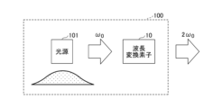
- FIG. 17 is a schematic diagram of a light source device 100 using a wavelength conversion element 10 of an embodiment.
- the light source device 100 includes a light source 101 such as a laser diode, and a wavelength conversion element 10 optically coupled to the light source 101.
- the wavelength conversion element 10 may have any of the configurations of the wavelength conversion elements 10A to 10I of the above-mentioned embodiments and the modified examples.
- the light source 101 emits light with an angular frequency of ⁇ 0.
- a second harmonic with an angular frequency of 2 ⁇ 0 is generated by the interaction between the laser light incident on the wavelength conversion element 10 and the core 15, and is output from the wavelength conversion element 10.
- ultraviolet light can be emitted from the light source device 100 due to SHG in the wavelength conversion element 10.
- the light source device 100 is used as a highly efficient ultraviolet light source.
- FIG. 18 is a schematic diagram of an optical circuit 200 using the wavelength conversion element 10 of the embodiment.
- the optical circuit 200 has a light source 101, a mode converter 103 optically coupled to the light source 101, and a wavelength conversion element 10 optically coupled to the mode converter 103.
- the light of the fundamental mode of ⁇ 1 emitted from the light source 101 is converted to light of a higher mode by the mode converter 103.
- the mode converter 103 may be a Y-shaped waveguide formed of an optical waveguide, a directional coupler, a multimode interferometer, or the like.
- the mode converter 103 may be continuously connected to the wavelength conversion element 10, or a part of the wavelength conversion element 10 may be used as the mode converter 103.
- the mode-converted light of ⁇ 1 enters the wavelength conversion element 10 as pump light.
- An optical parametric process occurs due to the interaction between the pump light and the optical waveguide 20 of the wavelength conversion element 10, generating a photon of ⁇ 2 .
- the signal light generated in the optical parametric process is input to a circuit element 105 constituting a sensor circuit or the like.
- a signal light of a different wavelength may be input to the wavelength conversion element 10 together with the pump light output from the mode converter 103 to generate difference frequency generation or sum frequency generation.
- the optical circuit 200 realizes a highly sensitive sensor using the optical parametric process.
- the wavelength conversion element 10 is a waveguide wavelength converter using phase matching by a transverse mode, and can be integrated with the mode converter 103 and the light source 101. This realizes an optical circuit 200 with a simple configuration and good conversion efficiency.
- the configuration of polar member 11F or 11G of the fourth embodiment in Figures 13 and 14 may be applied to the polar member 11 in Figures 1, 10, and 11.
- the configuration of the third embodiment in Figure 11 may be combined with the configuration of the second embodiment in Figure 10.
- the wavelength conversion element of the embodiment can be applied to a light source device that outputs ultraviolet light or mid-infrared light that is difficult to generate by current injection.
- An embodiment of the present disclosure may include, for example, the following configuration.
- the first non-polar member contacts both side surfaces of the polar member at the cross section perpendicular to the optical axis of the optical waveguide. Item 2.
- the core includes a second non-polar member provided outside the first non-polar member as viewed from the polar member in the cross section perpendicular to the optical axis, the second non-polar member being in contact with a side surface of the first non-polar member; and The refractive index of the second non-polar member is greater than the refractive index of the first non-polar member.
- the wavelength conversion element according to item 2. (Item 4)
- the core further includes a third non-polar member disposed on an upper surface of the polar member and an upper surface of the first non-polar member, The refractive index of the third non-polar member is equal to or greater than the refractive index of the polar member.
- the wavelength conversion element according to any one of items 1 to 3. (Item 5)
- the polar member has a first polar member and a second polar member in a normal direction of the main surface of the substrate, the first polar member is disposed between the substrate and the second polar member;
- the refractive index of the second polar member is greater than the refractive index of the first polar member.
- the width of the core is a width in which the number of modes that can exist for a first frequency component of a first angular frequency is 3 or less, and a width in which the number of modes that can exist for a second frequency component of a second angular frequency higher than the first angular frequency is 2 or more.
- the width of the core is 200 nm or more and 2000 nm or less.
- the width of the core is 1.5 times or more and 4 times or less than the width of the polar member.
- Item 8 The wavelength conversion element according to any one of items 1 to 7.
- the polar member is formed of a wurtzite crystal having polarization in the c-axis direction.
- Item 9 The wavelength conversion element according to any one of items 1 to 8.
- the c-axis of the polar member is perpendicular to the major surface of the substrate.
- the wavelength conversion element according to item 9. (Item 11)
- the polar member is formed of Al x Ga 1-x N (where 0 ⁇ x ⁇ 1); The wavelength conversion element according to claim 1 .
- the first non-polar member is an amorphous layer.
- Item 12. A wavelength conversion element according to any one of items 1 to 11.
- the first non - polar member is one selected from the group consisting of Nb2O5 , Ta2O5 , TiO2 , HfO2 , ZrO2 , and Si3N4 ; Item 13.
- the wavelength conversion element according to any one of items 1 to 12. (Item 14) A laser element; a mode converter optically coupled to the laser element; Item 14.
- An optical circuit comprising: (Item 15) A laser element; A wavelength conversion element according to any one of items 1 to 13, which is optically coupled to the laser element;
- a light source device comprising:
- Substrate 501 Main surface 10, 10A to 10I Wavelength conversion element 11, 11F, 11G Polar member 111, 112 Side surface 116 First polar member 117 Second polar member 118 Third polar member 12 First non-polar member 13 Second non-polar member 14 Third non-polar member 15, 15A to 15I Core 16 Clad 20, 20A to 20I Optical waveguide 100
- Light source device 101 Light source 103 Mode converter 105 Circuit element 200
Landscapes
- Physics & Mathematics (AREA)
- Nonlinear Science (AREA)
- General Physics & Mathematics (AREA)
- Optics & Photonics (AREA)
- Optical Modulation, Optical Deflection, Nonlinear Optics, Optical Demodulation, Optical Logic Elements (AREA)
Abstract
Description
主面を有する基板と、
前記基板の前記主面に配置される光導波路と、
を備え、
前記光導波路のコアは、2次の非線形光学定数を有する極性部材と、前記基板の前記主面と平行な方向で前記極性部材と隣接して配置される第1非極性部材と、を含み、
前記光導波路の光軸と直交する断面で、前記極性部材の一方または両方の側面と前記第1非極性部材とが接している。
図1は、第1実施形態の波長変換素子10の模式的な斜視図、図2は、図1の光軸OXと直交する断面図である。図1、及び図2の座標系で、波長変換素子10の光軸OXと平行な方向をZ方向とし、光軸OXと直交するXY面内で基板5の表面に対する法線方向をY方向とする。
nmat(ω1)<nmat(ω2)
である。一方、コア15の実効屈折率の横モード依存性(モード分散)により、基本モードにおけるコア15の実効屈折率n00は、高次の横モードにおける実効屈折率nm0よりも大きく、
n00>nm0
となる。ここで、mはモード次数である。実効屈折率の横モード依存性を利用して、ポンプ光と信号光が感じるモードごとの実効屈折率を同等にすることで、
n00(ω1)=nm0(ω2)
を満たすことができる。すなわち、コア15内でのポンプ光と信号光は位相整合条件を満足し得る。

図4は、波長変換素子10の第1変形例としての波長変換素子10Aの模式図である。波長変換素子10Aは、基板5の主面501の上に、光導波路20Aを有する。光導波路20Aは、コア15Aとクラッド16を含む。コア15Aは、極性部材11と、極性部材11の両側の側面111と112に接して配置される第1非極性部材12とを有する。光軸OX(図1参照)と直交するXY断面で、極性部材11は、第1非極性部材12の間に挟まれている。図1及び図2の波長変換素子10と同様に、波長変換素子10Aはシンプルな構成を有する。極性部材11と第1非極性部材12をY方向に厚く形成することができ、結晶品質を向上させることができる。また、対称性が高い形をとることで、TM00モードとTM20モードそれぞれの電場強度が高い領域に極性材料を配置できる。
図5Aから図5Dは、波長変換素子10Aのコア15Aの作製工程図である。図5Aにおいて、基板5の主面501に、極性材料の層110を形成する。基板5は、サファイア基板、GaN基板、石英基板、光学ガラス基板、樹脂基板、シリコン酸化膜付きのシリコン基板など、適切な基板を選択できる。基板5は、好ましくはサファイア基板またはGaN基板である。極性材料の層110を比較的高い品質で形成することができる。極性材料として、AlN、GaN、AlGaN、ZnO等のウルツ鉱型結晶構造をもつ材料を用いる。800nm近傍の波長に対して、GaNの屈折率は2.35、AlNとZnOの屈折率は、それぞれ2.18と2.10である。スパッタリングおよび蒸着等の物理気相成長(PVD:Physical Vapor Deposition)法や、化学気相成長(CVD:Chemical Vapor Deposition)法により、結晶品質の良好な極性材料の層110が形成される。極性材料の層110としてAlGaNを成膜するときは、AlとGaの組成を調整して、所望の屈折率にしてもよい。極性材料の層110の厚さは、たとえば、300nm乃至1000nmにする。位相整合条件はコアの幅方向(X方向)の横モードを制御することで満たすことができるので、極性材料の層110を比較的厚くすることができる。これにより、極性材料の層110の結晶品質を高めることができる。
図6Aは、波長変換素子10の第2変形例の波長変換素子10Bの模式図である。波長変換素子10Bの光導波路20Bは、極性部材11と、第1非極性部材12Bとで構成されるコア15Bを有する。第1非極性部材12Bは、極性部材11の両側の側面111及び112と、上面に接している。図5Dの工程で、異方性エッチングの終了時点を制御することで、図6Aの形状のコア15Bが得られる。極性部材11の上面が露出する前に非極性材料の層120の異方性エッチングを終了することで、基板5の主面501上に非極性材料の薄膜121が残る。図6Aの形状のコア15Bは、極性部材11を削り過ぎることなく極性部材11の膜厚を維持できる点で有利である。また、非極性材料の薄膜121が残るようにすることで、極性部材11の側面と接する第1非極性部材12Bが削れることを低減することができる。これにより、実効屈折率の制御を容易に行うことができる。
図6Bは、波長変換素子10の第3変形例の波長変換素子10Cの模式図である。波長変換素子10Cの光導波路20Cは、基板5の主面501の上に、極性部材11Cと第1非極性部材12とで構成されるコア15Cを有する。第1非極性部材12Bは、極性部材11の両側の側面111及び112と、上面に接している。図5Bの工程で、極性材料の層110の異方性エッチングの終了時点を制御することで、図6Bの形状のコア15Cが得られる。基板5の主面501が露出する前に極性材料の層110の異方性エッチングを終了することで、基板5の主面501上に、極性材料の薄膜115が残るが、光をコア15Cの内部に効果的に閉じ込めることができる。図6Bの形状のコア15Cも、極性部材11を削り過ぎることなく、膜厚を確保できる点で有利である。
図6Cは、波長変換素子10のさらに別の変形例を示す模式図である。図6Aの構成と、図6Bの構成を組み合わせて波長変換素子10C'の構成にしてもよい。光導波路20C'は、基板5の主面501の上に、極性部材11Cと第1非極性部材12Bとで構成されるコア15C'を有する。第1非極性部材12Bは、極性材料の薄膜115と極性部材11Cの上面とを覆って設けられ、コア15C'を覆ってクラッド16が形成される。図6Cの構成でも、極性部材11Cを削り過ぎることなく、膜厚を確保できる。
図7は、位相整合条件を満たすコア幅を求めるモデル図である。この例では、図4のコア形状をモデルに採用する。基板5をサファイア、コア15の極性部材11をAlN、極性部材11の両側面を挟む第1非極性部材12をTa2O5、コア15を覆うクラッド16をAl2O3とする。これにより、コアの幅および高さ、コアの屈折率、クラッドの屈折率、および基板の屈折率が定義できる。これらの情報から、有限要素法により電磁界分布および実効屈折率を得ることができる。コア15の高さhを400nm、極性部材11の幅Wを300nmに固定し、第1非極性部材12の幅を変えてコア15の幅Wを変化させる。このモデルを用いて波長810nmの光(角周波数ω1)と、波長405nmの光(角周波数ω2(=2×ω1))に対するコア15の実効屈折率neffを計算する。上述したように、光導波路20で、実効屈折率neffの横モード依存性(モード分散)を利用して位相整合させるために、波長810nmの基本波TM00モードと、波長405nmの第2高調波TM20モードにおける実効屈折率neffが同じか、または十分に近接している必要がある。
図10は、第2実施形態の波長変換素子10Dの断面図である。波長変換素子10Dは、基板5の主面501の上に配置される光導波路20Dを有する。光導波路20Dのコア15Dは、2次の非線形光学定数を有する極性部材11と、XY断面の主面501と平行な方向(X方向)で極性部材11と隣接して配置される第1非極性部材12と、第1非極性部材12の外側に配置されて第1非極性部材12の側面と接する第2非極性部材13と、を有する。第2非極性部材13の屈折率は第1非極性部材12の屈折率よりも大きい。第1非極性部材12の「外側」とは、XY断面のX方向で見たときに極性部材11を中心として外側という意味である。このとき、第1非極性部材12は極性部材11と第2非極性部材13との間に位置する。
図11は、第3実施形態の波長変換素子10EのXY断面図である。波長変換素子10Eは、基板5の主面501の上に配置される光導波路20Eを有する。光導波路20Eのコア15Eは、極性部材11の上面と第1非極性部材12の上面に配置される第3非極性部材14をさらに有する。第3非極性部材14の屈折率の大きさは、極性部材11の屈折率の大きさ以上である。この構成では、極性部材11以上の屈折率を有する第3非極性部材14により、光は基板5よりも第3非極性部材14の近くで導波できる。したがって、結晶状態が良好なコア15の上側に光をより集中させて損失を低減し、変換効率が向上する。コア15の上側は、基板5とコア15の界面よりも極性部材11の結晶品質が良好だからである。たとえば、極性部材11にAlNを用い、第1非極性部材12にTa2O5を用い、第3非極性部材14にNb2O5を用いると、極性部材11と第1非極性部材12の屈折率はほぼ同じになり、第3非極性部材14の屈折率が、極性部材11と第1非極性部材12の屈折率以上になる。
図13は、第4実施形態の波長変換素子10Fの断面図である。波長変換素子10Fは、基板5の主面501の上に配置される光導波路20Fを有する。光導波路20Fのコア15Fは、極性部材11Fと、極性部材11Fの両側の側面で接する第1非極性部材12を有する。極性部材11Fは、基板5の主面501の法線方向に、第1極性部材116と、第2極性部材117及び/または第3極性部材118と、を有する。第1極性部材116は、基板5と、第2極性部材117または第3極性部材118との間に配置される。第2極性部材117及び第3極性部材118の屈折率は、それぞれ第1極性部材116の屈折率よりも大きい。第2極性部材117と第3極性部材118のいずれか一方だけを用いてもよい。
第1実施形態から第4実施形態またはそれらの変形例において、極性部材の高さと非極性部材の高さはかならずしも一致しなくてもよい。例えば、極性部材の高さは非極性部材の高さよりも高くても低くてもよい。角周波数ω1と角周波数ω2の値、極性部材と非極性部材の材料の組み合わせおよび極性部材と非極性部材の幅などに応じて極性部材の高さと非極性部材の高さを適宜設定することができる。以下にその一例を示す。
図17は、実施形態の波長変換素子10を用いた光源装置100の模式図である。光源装置100は、レーザダイオード等の光源101と、光源101と光学的に結合する波長変換素子10と、を含む。波長変換素子10は、上述した実施例、及び変形例の波長変換素子10Aから10Iのいずれの構成を有していてもよい。光源101は角周波数ω0の光を出射する。波長変換素子10に入射したレーザ光とコア15との相互作用により、角周波数2×ω0の第2高調波が生成され、波長変換素子10から出力される。たとえば、青色波長帯の光を出射する光源101を用いると、波長変換素子10におけるSHGにより、光源装置100から紫外光を出射することができる。光源装置100は高効率の紫外光源として用いられる。
(項1)
主面を有する基板と、
前記基板の前記主面に配置される光導波路と、
を備え、
前記光導波路のコアは、2次の非線形光学定数を有する極性部材と、前記基板の前記主面と平行な方向で前記極性部材と隣接して配置される第1非極性部材と、を含み、
前記光導波路の光軸と直交する断面で、前記極性部材の一方または両方の側面と前記第1非極性部材とが接している、
波長変換素子。
(項2)
前記第1非極性部材は、前記光導波路の前記光軸と直交する前記断面で、前記極性部材の前記両方の側面と接する、
項1に記載の波長変換素子。
(項3)
前記コアは、前記光軸と直交する前記断面で前記極性部材から見て前記第1非極性部材の外側に、前記第1非極性部材の側面と接して設けられる第2非極性部材、
をさらに有し、
前記第2非極性部材の屈折率は、前記第1非極性部材の屈折率よりも大きい、
項2に記載の波長変換素子。
(項4)
前記コアは、前記極性部材の上面と前記第1非極性部材の上面に配置される第3非極性部材をさらに有し、
前記第3非極性部材の屈折率の大きさは、前記極性部材の屈折率の大きさ以上である、
項1から3のいずれかに記載の波長変換素子。
(項5)
前記極性部材は、前記基板の前記主面の法線方向に、第1極性部材と、第2極性部材と、を有し、
前記第1極性部材は、前記基板と前記第2極性部材との間に配置され、
前記第2極性部材の屈折率は、前記第1極性部材の屈折率よりも大きい、
項1から4のいずれかに記載の波長変換素子。
(項6)
前記光導波路の前記光軸と直交する前記断面において、前記コアの幅は、第1角周波数の第1周波数成分に対して存在可能なモード数が3以下となる幅であり、かつ、前記第1角周波数よりも大きな第2の角周波数の第2周波数成分に対して存在可能なモード数が2以上となる幅である、
項1から5のいずれか1項に記載の波長変換素子。
(項7)
前記光軸と直交する前記断面で、前記コアの幅は200nm以上2000nm以下である、
項1から6のいずれか1項に記載の波長変換素子。
(項8)
前記光軸と直交する前記断面で、前記コアの幅は前記極性部材の幅の1.5倍以上4倍以下である、
項1から7のいずれかに記載の波長変換素子。
(項9)
前記極性部材は、c軸方向に分極をもつウルツ鉱型結晶で形成されている、
項1から8のいずれかに記載の波長変換素子。
(項10)
前記極性部材のc軸は前記基板の前記主面に対して垂直である、
項9に記載の波長変換素子。
(項11)
前記極性部材は、AlxGa1-xN(ただし、0≦x≦1)で形成されている、
請求項1から10のいずれかに記載の波長変換素子。
(項12)
前記第1非極性部材は、アモルファス層である、
項1から11のいずれかに記載の波長変換素子。
(項13)
前記第1非極性部材は、Nb2O5、Ta2O5、TiO2、HfO2、ZrO2、Si3N4からなる群から選択される1つである、
項1から12のいずれかに記載の波長変換素子。
(項14)
レーザ素子と、
前記レーザ素子と光学的に結合するモード変換器と、
前記モード変換器と光学的に結合する、項1から13のいずれかに記載の波長変換素子と、
を備える、光回路。
(項15)
レーザ素子と、
前記レーザ素子と光学的に結合する項1から13のいずれかに記載の波長変換素子と、
を備える光源装置。
501 主面
10、10A乃至10I 波長変換素子
11、11F、11G 極性部材
111、112 側面
116 第1極性部材
117 第2極性部材
118 第3極性部材
12 第1非極性部材
13 第2非極性部材
14 第3非極性部材
15、15A乃至15I コア
16 クラッド
20、20A乃至20I 光導波路
100 光源装置
101 光源
103 モード変換器
105 回路素子
200 光回路
Claims (15)
- 主面を有する基板と、
前記基板の前記主面に配置される光導波路と、
を備え、
前記光導波路のコアは、2次の非線形光学定数を有する極性部材と、前記基板の前記主面と平行な方向で前記極性部材と隣接して配置される第1非極性部材と、を含み、
前記光導波路の光軸と直交する断面で、前記極性部材の一方または両方の側面と前記第1非極性部材とが接している、
波長変換素子。 - 前記第1非極性部材は、前記光導波路の前記光軸と直交する前記断面で、前記極性部材の前記両方の側面と接する、
請求項1に記載の波長変換素子。 - 前記コアは、前記光軸と直交する前記断面で前記極性部材から見て前記第1非極性部材の外側に、前記第1非極性部材の側面と接して設けられる第2非極性部材、
をさらに有し、
前記第2非極性部材の屈折率は、前記第1非極性部材の屈折率よりも大きい、
請求項2に記載の波長変換素子。 - 前記コアは、前記極性部材の上面と前記第1非極性部材の上面に配置される第3非極性部材をさらに有し、
前記第3非極性部材の屈折率の大きさは、前記極性部材の屈折率の大きさ以上である、
請求項1に記載の波長変換素子。 - 前記極性部材は、前記基板の前記主面の法線方向に、第1極性部材と、第2極性部材と、を有し、
前記第1極性部材は、前記基板と前記第2極性部材との間に配置され、
前記第2極性部材の屈折率は、前記第1極性部材の屈折率よりも大きい、
請求項1から4のいずれか1項に記載の波長変換素子。 - 前記光導波路の前記光軸と直交する前記断面において、前記コアの幅は、第1角周波数の第1周波数成分に対して存在可能なモード数が3以下となる幅であり、かつ、前記第1角周波数よりも大きな第2の角周波数の第2周波数成分に対して存在可能なモード数が2以上となる幅である、
請求項1から4のいずれか1項に記載の波長変換素子。 - 前記光軸と直交する前記断面で、前記コアの幅は200nm以上2000nm以下である、
請求項1から4のいずれか1項に記載の波長変換素子。 - 前記光軸と直交する前記断面で、前記コアの幅は前記極性部材の幅の1.5倍以上4倍以下である、
請求項1から4のいずれか1項に記載の波長変換素子。 - 前記極性部材は、c軸方向に分極をもつウルツ鉱型結晶で形成されている、
請求項1から4のいずれか1項に記載の波長変換素子。 - 前記極性部材のc軸は前記基板の前記主面に対して垂直である、
請求項9に記載の波長変換素子。 - 前記極性部材は、AlxGa1-xN(ただし、0≦x≦1)で形成されている、
請求項9に記載の波長変換素子。 - 前記第1非極性部材は、アモルファス層である、
請求項1から4のいずれか1項に記載の波長変換素子。 - 前記第1非極性部材は、Nb2O5、Ta2O5、TiO2、HfO2、ZrO2、Si3N4からなる群から選択される1つである、請求項1から4の何れか1項に記載の波長変換素子。
- レーザ素子と、
前記レーザ素子と光学的に結合するモード変換器と、
前記モード変換器と光学的に結合する請求項1から4の何れか1項に記載の波長変換素子と、
を備える、光回路。 - レーザ素子と、
前記レーザ素子と光学的に結合する請求項1から4の何れか1項に記載の波長変換素子と、
を備える光源装置。
Priority Applications (2)
| Application Number | Priority Date | Filing Date | Title |
|---|---|---|---|
| JP2025530154A JPWO2025005104A1 (ja) | 2023-06-27 | 2024-06-26 | |
| EP24831964.2A EP4737999A1 (en) | 2023-06-27 | 2024-06-26 | Wavelength conversion element, optical circuit using same, and light source device |
Applications Claiming Priority (2)
| Application Number | Priority Date | Filing Date | Title |
|---|---|---|---|
| JP2023-105432 | 2023-06-27 | ||
| JP2023105432 | 2023-06-27 |
Publications (1)
| Publication Number | Publication Date |
|---|---|
| WO2025005104A1 true WO2025005104A1 (ja) | 2025-01-02 |
Family
ID=93939260
Family Applications (1)
| Application Number | Title | Priority Date | Filing Date |
|---|---|---|---|
| PCT/JP2024/023094 Ceased WO2025005104A1 (ja) | 2023-06-27 | 2024-06-26 | 波長変換素子、これを用いた光回路、及び光源装置 |
Country Status (3)
| Country | Link |
|---|---|
| EP (1) | EP4737999A1 (ja) |
| JP (1) | JPWO2025005104A1 (ja) |
| WO (1) | WO2025005104A1 (ja) |
Citations (3)
| Publication number | Priority date | Publication date | Assignee | Title |
|---|---|---|---|---|
| US20160178983A1 (en) * | 2013-12-03 | 2016-06-23 | Karlsruher Institut Fuer Technologie | Second-order optical nonlinear material |
| CN112099286A (zh) * | 2020-09-29 | 2020-12-18 | 清华大学 | 光学谐波产生器及其制备方法 |
| JP2021134122A (ja) * | 2020-02-27 | 2021-09-13 | 株式会社東芝 | 窒化物結晶、光学装置、半導体装置、窒化物結晶の製造方法 |
-
2024
- 2024-06-26 EP EP24831964.2A patent/EP4737999A1/en active Pending
- 2024-06-26 WO PCT/JP2024/023094 patent/WO2025005104A1/ja not_active Ceased
- 2024-06-26 JP JP2025530154A patent/JPWO2025005104A1/ja active Pending
Patent Citations (3)
| Publication number | Priority date | Publication date | Assignee | Title |
|---|---|---|---|---|
| US20160178983A1 (en) * | 2013-12-03 | 2016-06-23 | Karlsruher Institut Fuer Technologie | Second-order optical nonlinear material |
| JP2021134122A (ja) * | 2020-02-27 | 2021-09-13 | 株式会社東芝 | 窒化物結晶、光学装置、半導体装置、窒化物結晶の製造方法 |
| CN112099286A (zh) * | 2020-09-29 | 2020-12-18 | 清华大学 | 光学谐波产生器及其制备方法 |
Non-Patent Citations (1)
| Title |
|---|
| 12 September 2021 (2021-09-12), K. HONDA, S. UMEDA, K. SHOJIKI: "Design of Transverse Quasi-Phase-Matched HfO2/AlN Waveguide for 230-nm Far-UV Second Harmonic Generation", XP009559665 * |
Also Published As
| Publication number | Publication date |
|---|---|
| EP4737999A1 (en) | 2026-05-06 |
| JPWO2025005104A1 (ja) | 2025-01-02 |
Similar Documents
| Publication | Publication Date | Title |
|---|---|---|
| Chen et al. | Advances in lithium niobate photonics: development status and perspectives | |
| Wen et al. | Fabrication and photonic applications of Si-integrated LiNbO3 and BaTiO3 ferroelectric thin films | |
| US11754908B2 (en) | Devices and methods for giant single-photon nonlinearities | |
| US7373059B2 (en) | Compact, single chip-based, entangled polarization-state photon sources and methods for generating photons in entangled polarization states | |
| WO2010093783A2 (en) | Surface plasmon enhanced optical devices for integrated photonics | |
| JP7160194B2 (ja) | 波長変換素子 | |
| WO2009035585A2 (en) | Hybrid integrated source of polarization-entangled photons | |
| CN113515000B (zh) | 一种超宽带能量-时间纠缠双光子态的产生方法 | |
| WO2021149183A1 (ja) | 光デバイス | |
| JP7295467B2 (ja) | 光学素子及びその製造方法 | |
| US9291874B2 (en) | Optical deflection element and optical deflection device | |
| Soref et al. | Classical and quantum photonic sources based upon a nonlinear GaP/Si-superlattice micro-ring resonator | |
| CN117215098B (zh) | 基于光学超晶格电光长周期光栅的滤波器及其制备方法 | |
| CN113612108B (zh) | 一种基于斜切非线性晶体脊型波导的频率转换器及其制备方法 | |
| De Leonardis et al. | Efficient second-harmonic generation in Si-GaP asymmetric coupled-quantum-well waveguides | |
| WO2025005104A1 (ja) | 波長変換素子、これを用いた光回路、及び光源装置 | |
| JP2015210492A (ja) | 波長変換素子 | |
| JP2016173429A (ja) | 波長変換素子 | |
| JP2010197802A (ja) | 第二高調波発生素子及びその製造方法 | |
| Kang et al. | Wavelength Conversion Efficiency Enhancement in Modal Phase Matched $\chi^{\hbox {{(2)}}} $ Nonlinear Waveguides | |
| Honda et al. | Second harmonic generation in horizontally aligned AlN/SiN x hybrid waveguide for integrated wavelength converter | |
| Takano et al. | Highly effective in-plane channel-drop filters in two-dimensional heterostructure photonic-crystal slab | |
| JP7740370B2 (ja) | 光デバイス | |
| Liu et al. | Hybrid scandium aluminum nitride/silicon nitride integrated photonic circuits | |
| WO2024236745A1 (ja) | 非線形光導波路 |
Legal Events
| Date | Code | Title | Description |
|---|---|---|---|
| 121 | Ep: the epo has been informed by wipo that ep was designated in this application |
Ref document number: 24831964 Country of ref document: EP Kind code of ref document: A1 |
|
| ENP | Entry into the national phase |
Ref document number: 2025530154 Country of ref document: JP Kind code of ref document: A |
|
| WWE | Wipo information: entry into national phase |
Ref document number: 2025530154 Country of ref document: JP |
|
| WWE | Wipo information: entry into national phase |
Ref document number: 2024831964 Country of ref document: EP |
|
| NENP | Non-entry into the national phase |
Ref country code: DE |
|
| ENP | Entry into the national phase |
Ref document number: 2024831964 Country of ref document: EP Effective date: 20260127 |
|
| ENP | Entry into the national phase |
Ref document number: 2024831964 Country of ref document: EP Effective date: 20260127 |