WO2025004841A1 - 光電変換装置及び該光電変換装置を有する光電変換システム - Google Patents
光電変換装置及び該光電変換装置を有する光電変換システム Download PDFInfo
- Publication number
- WO2025004841A1 WO2025004841A1 PCT/JP2024/021596 JP2024021596W WO2025004841A1 WO 2025004841 A1 WO2025004841 A1 WO 2025004841A1 JP 2024021596 W JP2024021596 W JP 2024021596W WO 2025004841 A1 WO2025004841 A1 WO 2025004841A1
- Authority
- WO
- WIPO (PCT)
- Prior art keywords
- photoelectric conversion
- circuit
- signal
- conversion device
- waveform shaping
- Prior art date
- Legal status (The legal status is an assumption and is not a legal conclusion. Google has not performed a legal analysis and makes no representation as to the accuracy of the status listed.)
- Ceased
Links
Images










Classifications
-
- H—ELECTRICITY
- H04—ELECTRIC COMMUNICATION TECHNIQUE
- H04N—PICTORIAL COMMUNICATION, e.g. TELEVISION
- H04N25/00—Circuitry of solid-state image sensors [SSIS]; Control thereof
- H04N25/70—SSIS architectures; Circuits associated therewith
- H04N25/76—Addressed sensors, e.g. MOS or CMOS sensors
- H04N25/77—Pixel circuitry, e.g. memories, A/D converters, pixel amplifiers, shared circuits or shared components
- H04N25/772—Pixel circuitry, e.g. memories, A/D converters, pixel amplifiers, shared circuits or shared components comprising A/D, V/T, V/F, I/T or I/F converters
- H04N25/773—Pixel circuitry, e.g. memories, A/D converters, pixel amplifiers, shared circuits or shared components comprising A/D, V/T, V/F, I/T or I/F converters comprising photon counting circuits, e.g. single photon detection [SPD] or single photon avalanche diodes [SPAD]
-
- G—PHYSICS
- G01—MEASURING; TESTING
- G01J—MEASUREMENT OF INTENSITY, VELOCITY, SPECTRAL CONTENT, POLARISATION, PHASE OR PULSE CHARACTERISTICS OF INFRARED, VISIBLE OR ULTRAVIOLET LIGHT; COLORIMETRY; RADIATION PYROMETRY
- G01J1/00—Photometry, e.g. photographic exposure meter
- G01J1/42—Photometry, e.g. photographic exposure meter using electric radiation detectors
- G01J1/44—Electric circuits
-
- H—ELECTRICITY
- H04—ELECTRIC COMMUNICATION TECHNIQUE
- H04N—PICTORIAL COMMUNICATION, e.g. TELEVISION
- H04N25/00—Circuitry of solid-state image sensors [SSIS]; Control thereof
- H04N25/70—SSIS architectures; Circuits associated therewith
- H04N25/709—Circuitry for control of the power supply
-
- G—PHYSICS
- G01—MEASURING; TESTING
- G01J—MEASUREMENT OF INTENSITY, VELOCITY, SPECTRAL CONTENT, POLARISATION, PHASE OR PULSE CHARACTERISTICS OF INFRARED, VISIBLE OR ULTRAVIOLET LIGHT; COLORIMETRY; RADIATION PYROMETRY
- G01J1/00—Photometry, e.g. photographic exposure meter
- G01J1/42—Photometry, e.g. photographic exposure meter using electric radiation detectors
- G01J1/44—Electric circuits
- G01J2001/4413—Type
- G01J2001/442—Single-photon detection or photon counting
-
- G—PHYSICS
- G01—MEASURING; TESTING
- G01J—MEASUREMENT OF INTENSITY, VELOCITY, SPECTRAL CONTENT, POLARISATION, PHASE OR PULSE CHARACTERISTICS OF INFRARED, VISIBLE OR ULTRAVIOLET LIGHT; COLORIMETRY; RADIATION PYROMETRY
- G01J1/00—Photometry, e.g. photographic exposure meter
- G01J1/42—Photometry, e.g. photographic exposure meter using electric radiation detectors
- G01J1/44—Electric circuits
- G01J2001/4446—Type of detector
- G01J2001/446—Photodiode
- G01J2001/4466—Avalanche
Definitions
- the present invention relates to a photoelectric conversion device and a photoelectric conversion system having the photoelectric conversion device.
- a photoelectric conversion device uses avalanche (electron avalanche) multiplication to detect weak light at the single photon level.
- Patent Document 1 discloses a photoelectric conversion device that performs so-called clock recharge driving.
- the sensitivity of each pixel may be adjusted to, for example, a low sensitivity in order to prevent pile-up under high illuminance. In this case, there is a concern that image quality may deteriorate if the photon detection period is shortened or the clock frequency is lowered.
- One aspect of the present invention is a photoelectric conversion device that includes a photoelectric conversion element that generates a photon detection signal by avalanche multiplication, a circuit that controls a first state in which a first terminal of the photoelectric conversion element is connected to a power supply voltage and a second state in which a resistance between the first terminal and the power supply voltage is higher than that in the first state, a counter circuit connected to the photoelectric conversion element, a waveform shaping circuit disposed between the photoelectric conversion element and the counter circuit, and a gating circuit connected between an output node of the waveform shaping circuit and an input node of the counter circuit, and that controls whether or not an output signal of the waveform shaping circuit is input to the counter circuit.
- a photoelectric conversion device comprising: a photoelectric conversion element that generates a photon detection signal by avalanche multiplication; a resistive element provided between a first terminal of the photoelectric conversion element and a power supply voltage; a counter circuit connected to an output node of the photoelectric conversion element; a waveform shaping circuit provided between the photoelectric conversion element and the counter circuit; and a gating circuit provided between the output node of the waveform shaping circuit and the input node of the counter circuit that controls whether or not an output signal of the waveform shaping circuit is input to the counter circuit, wherein during one standby state, there is a first period during which the output signal of the waveform shaping circuit is counted, and a second period during which the gating circuit is controlled not to count the output signal of the waveform shaping circuit, and the device comprises a circuit that counts the number of first periods during which the output signal of the waveform shaping circuit is counted.
- the present invention makes it possible to adjust the sensitivity of a photoelectric conversion device while suppressing image degradation.
- FIG. 1 is a schematic configuration diagram of a photoelectric conversion device according to a first embodiment.
- 1 is a circuit diagram illustrating an example of a configuration of a photoelectric conversion device according to a first embodiment.
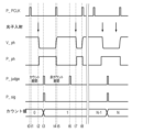
- FIG. 2 is an operation sequence diagram of the photoelectric conversion device according to the first embodiment.
- 11 is a circuit diagram illustrating an example of a configuration of a photoelectric conversion device according to a second embodiment.
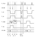
- FIG. 11 is an operation sequence diagram of a photoelectric conversion device according to a second embodiment.
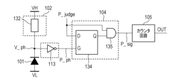
- 13 is a circuit diagram illustrating an example of a configuration of a photoelectric conversion device according to a third embodiment.
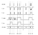
- FIG. 11 is an operation sequence diagram of a photoelectric conversion device according to a third embodiment.
- FIG. 13 is a schematic diagram of a photoelectric conversion device according to a fourth embodiment.
- FIG. 13 is a circuit diagram illustrating an example of a configuration of a photoelectric conversion device according to a fourth embodiment.
- FIG. 13 is an operation sequence diagram of a photoelectric conversion device according to a fourth embodiment.
- FIG. 13 is a schematic diagram of a photoelectric conversion device according to a fifth embodiment.
- 13 is a circuit diagram illustrating an example of the configuration of a photoelectric conversion device according to a fifth embodiment.
- FIG. 13 is an operation sequence diagram of a photoelectric conversion device according to a fifth embodiment.
- FIG. 13 is a functional block diagram of a photoelectric conversion system according to a sixth embodiment.
- FIG. 13 is a functional block diagram of a photoelectric conversion system according to a seventh embodiment.
- FIG. 13 is a functional block diagram of a photoelectric conversion system according to an eighth embodiment.
- FIG. 13 is a circuit diagram illustrating an example of a configuration of a photoelectric conversion device according to a fourth embodiment.
- FIG. 13 is an operation sequence diagram of a photoelectric conversion device
- FIG. 13 is a functional block diagram of a photoelectric conversion system according to an eighth embodiment.
- FIG. 13 is a functional block diagram of a photoelectric conversion system according to a ninth embodiment.
- FIG. 23 is a functional block diagram of a photoelectric conversion system according to a tenth embodiment.
- FIG. 23 is a functional block diagram of a photoelectric conversion system according to an eleventh embodiment.
- FIG. 23 is a functional block diagram of a photoelectric conversion system according to an eleventh embodiment.
- Fig. 1 is a schematic diagram of one pixel of the photoelectric conversion device.
- Fig. 2 is a specific circuit diagram configuration example, and
- Fig. 3 is an operation sequence diagram of the circuit configuration of Fig. 2.
- the avalanche photodiode (APD) 101 is a photodiode that generates pairs of charges in response to incident light through photoelectric conversion.
- a voltage VL first voltage
- a voltage VH second voltage
- a reverse bias voltage that causes avalanche multiplication is applied to the APD 101.
- APD 101 When a reverse bias voltage is supplied to the APD 101, it can operate in either Geiger mode or linear mode. In Geiger mode, APD 101 is operated by applying a voltage greater than the breakdown voltage to the anode and cathode. In linear mode, APD 101 is operated by setting the potential difference between the anode and cathode to a voltage difference close to or less than the breakdown voltage.
- An APD operated in Geiger mode is called a SPAD. For example, voltage VL (first voltage) is -30V, and voltage VH (second voltage) is 1V.
- the quench element 102 is connected between a power supply that supplies a voltage VH and the cathode terminal of the APD 101.
- the quench element 102 functions as a load circuit during signal multiplication by avalanche multiplication, and performs a quenching operation that suppresses avalanche multiplication by suppressing the voltage supplied to the APD 101.
- the output signal of the APD 101 is input to the waveform shaping circuit 103 in the subsequent stage.
- the waveform shaping circuit 103 shapes the potential change of the cathode of the APD 101 when a photon is detected, and outputs a pulse signal P_ph.
- an inverter circuit 113 is used as the waveform shaping circuit 103. While FIG. 2 shows an example in which one inverter circuit is used as the waveform shaping section, a circuit in which multiple inverters are connected in series may be used, or other circuits that have a waveform shaping effect may be used.
- the processing circuit 104 which is provided after the waveform shaping circuit 103, receives the pulse signal P_ph output from the waveform shaping circuit 103 and the judge signal P_judge output from the pulse generation circuit 106, and outputs a pulse signal P_sig.
- the counter circuit 105 counts the pulse signal P_sig output from the processing circuit and holds the count value.
- the processing circuit 104 is connected between the output node of the waveform shaping circuit 103 and the input node of the counter circuit 105, and is a gating circuit that controls whether or not the output signal of the waveform shaping circuit 103 is input to the counter circuit 105.
- FIG. 2 shows an example of a specific circuit configuration that realizes the schematic configuration diagram of each pixel shown in FIG. 1.
- each pixel of the photoelectric conversion device shown in FIG. 2 has one inverter circuit 113 as the waveform shaping circuit 103.
- the pulse signal P_ph, which is the output of the inverter circuit 113, and the judge signal P_judge are input to an AND circuit 114 that constitutes the processing circuit 104.
- the AND circuit 114 outputs the logical product of the pulse signal P_ph and the judge signal P_judge as a pulse signal P_sig.
- the quench element 102 has a switch 112 controlled by a clock signal P_PCLK, and drives the APD 101 with a clock recharge. That is, the clock signal P_PCLK controls the APD 101 to a standby state (second state) in which avalanche multiplication is possible, and a charge state (first state) in which the APD 101 is controlled to a state in which avalanche multiplication is possible.
- the switch In the charge state, the switch is in an on state, and the cathode (first terminal) of the APD 101 is connected to the power supply voltage.
- the standby state the switch is in an off state, and the cathode of the APD 101 is not connected to the power supply voltage.
- the resistance between the cathode of the APD 101 and the power supply voltage is high compared to the charge state.
- avalanche multiplication occurs, and the voltage of V_ph drops.
- the clock signal P_PCLK is input to switch 112, which turns switch 112 on, charges the voltage, and returns the voltage of V_ph to its initial state.
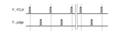
- the count period (first period) and non-count period (second period) are defined by the clock signal P_PCLK and the judge signal P_judge.
- the count period is a period during which the counter circuit 105 counts the signal output from the waveform shaping circuit 103 based on the photons detected by the APD 101.
- the non-count period is a period during which the signal output from the waveform shaping circuit 103 is not counted.
- the count period is the period from the falling edge of the pulse of the clock signal P_PCLK to the falling edge of the pulse of the judge signal P_judge.
- the non-count period is the period from the falling edge of the pulse of the judge signal P_judge to the falling edge of the pulse of the clock signal P_PCLK.
- a clock signal P_PCLK is input to the quench element 102, and the APD goes into standby mode at time t1.
- avalanche multiplication occurs, causing V_ph to drop, and when it exceeds the decision threshold, the pulse signal P_ph rises.
- a pulse signal P_sig which is the logical product of the pulse signal P_ph and the judge signal P_judge, is output.
- the clock signal P_PCLK is again input to the switch 112 of the quench element, and the APD 101 enters a charged state. In other words, V_ph is charged, and when it exceeds the judgement threshold, P_ph falls.
- the judge signal P_judge is input to the AND circuit 114 at time t6.
- the pulse signal V_ph is charged with a reverse bias voltage, and the pulse signal P_ph is Low. Therefore, the pulse signal P_sig, which is the output of the AND circuit 114, is also Low. After that, the judge signal P_judge falls.
- the non-counting period begins with the input of the judge signal P_judge.
- the pulse signal P_ph rises in response to the drop in V_ph, but since the judge signal P_judge is Low, the pulse signal P_sig is also Low.
- the clock signal P_PCLK is input, and when V_ph is charged beyond the judgment threshold, the pulse signal P_ph falls.
- no photons are incident on the APD 101 during the counting period, and photons are only incident on the APD 101 during the non-counting period, so no photon detection signal is counted.
- the pulse signal P_ph is in a high state when the judge signal P_judge is input to the processing circuit, one pulse is input to the counter circuit 105 as the pulse signal P_sig. Conversely, if the pulse signal P_ph is in a low state, the pulse signal P_sig is not input to the counter circuit 105, and no counting is performed. Therefore, the sensitivity of the pixel can be adjusted by adjusting the timing at which the judge signal P_judge is input to the processing circuit 104. In other words, during one standby state period, there is a count period in which the pulse signal P_sig is counted from the input of the judge signal P_judge, and a non-count period in which the pulse signal P_sig is not counted.
- a method for adjusting the sensitivity of each pixel in a conventional circuit that performs clock recharge drive is to lower the frequency of the clock signal P_PCLK and reduce the number of clock signals P_PCLK per unit time. In this case, there are concerns that the tonal range may decrease and the signal-to-noise ratio may deteriorate. There is also a method for shortening the charge accumulation period while maintaining the frequency of the clock signal P_PCLK, but this can cause degradation of image quality, such as the appearance of flicker, as periods during the exposure period occur when no charge is accumulated. With this method, it is possible to adjust the sensitivity of the photoelectric conversion device without causing such degradation of image quality.
- the photoelectric conversion device according to the second embodiment will be described with reference to Figures 4 and 5.
- the photoelectric conversion device according to the second embodiment uses a gating circuit different from that of the photoelectric conversion device according to the first embodiment.
- FIG. 4 is a specific circuit diagram of the photoelectric conversion device according to this embodiment.
- FIG. 5 is an operation sequence diagram of the circuit configuration of FIG. 4.
- the count period in which the counter circuit 105 counts the output signal of the waveform shaping circuit 103 and the non-count period in which the counter circuit 105 does not count the output signal of the waveform shaping circuit 103 are defined by the High and Low of the judge signal P_judge.
- the count period is defined by the period in which the judge signal P_judge is High. Note that the period in which the judge signal P_judge is High during one recharge period must be set to once or less. This is because if the judge signal P_judge is High two or more times during the recharge period, there is a possibility that the pulse signal P_sig will be output two or more times for one photon.
- the photoelectric conversion device has a D latch circuit 124 and an AND circuit 125 as the processing circuit 104.
- the output signal of the waveform shaping circuit is input to the input G of the D latch circuit 124, and the judge signal P_judge is input to the input D.
- the output Q and the judge signal P_judge are input to the AND circuit 125, and the output signal of the AND circuit 125 is input to the counter circuit 105 as the pulse signal P_sig.
- the input G of the D latch circuit 124 is High, it outputs the input D from the output Q.
- the circuit outputs the input D immediately before the change in input G from the output Q, and holds that value in the output Q while the input G is Low.
- a clock signal P_PCLK is input to the switch 112 of the quench element, and at time t1 the APD 101 goes into standby mode.
- a judge signal P_judge is input to the input D of the D latch circuit 124 and one of the input terminals of the AND circuit 125, and the count period begins.
- avalanche multiplication occurs, causing V_ph to drop, and when it exceeds the judgment threshold, the pulse signal P_ph rises.
- the high pulse signal P_ph is input to the input G of the D latch circuit 124.
- the judge signal P_judge of the input D is input to the other input terminal of the AND circuit 125 as the output Q of the D latch circuit 124. Therefore, H is output as the pulse signal P_sig, which is the logical AND of the judge signals P_judge.
- the judge signal P_judge controls the gating operation of the processing circuit 104, which functions as a gating circuit.
- the judge signal P_judge falls, and the count period ends.
- the pulse signal P_sig also falls.
- the clock signal P_PCLK is again input to the switch 112 of the quench element, and the APD 101 enters a charging state.
- V_ph is charged, and when it exceeds the decision threshold, P_ph falls.
- P_ph falls.
- photons are incident on the APD 101 during the counting period, so a signal based on the detection of photons is counted.
- APD 101 is charged, and in the next standby state period starting at time t7, the judge signal P_judge input to AND circuit 125 goes High at time t8, starting the count period.
- a High judge signal P_judge is input to one input terminal of AND circuit 125.
- V_ph is in a state where it is charged with a reverse bias voltage, and the pulse signal P_ph is Low.
- the input G of D latch circuit 124 is Low, and at this time the output Q is Low.
- the output Q is input to the other input terminal of AND circuit 125. Therefore, the pulse signal P_sig, which is the output of AND circuit 125, is also Low.
- the judge signal P_judge falls at time t9, and the count period ends.
- V_ph falls, and when it exceeds the judgment threshold, P_ph rises.
- a clock signal P_PCLK is input to the switch 112 of the quench element, and when V_ph is charged beyond the judgment threshold, P_ph falls. Since the judge signal P_judge is low from time t9 to time t11, the pulse signal P_sig output during this period is also low. During this standby state, no photons are incident on the APD 101 during the count period, and photons are only incident on the APD 101 during the non-count period, so no photon detection signal is counted.
- the next standby period begins at time t7.
- the count period can be set at any position during one standby state period.
- the count period was stopped at a specified time to create a non-count period.
- the count period and non-count period are always set in that order during one standby state period.
- a photoelectric conversion device according to a third embodiment will be described with reference to Fig. 6 and Fig. 7.
- a resistive element 132 is arranged as the quench element 102.
- the quench element is not controlled by a clock signal.
- a photoelectric conversion device using a so-called passive recharge driven SPAD will be described.
- FIG. 6 is a specific circuit diagram configuration example
- FIG. 7 is an operation sequence diagram of the circuit configuration of FIG. 6.
- the processing circuit 104 includes a D latch circuit 134 and an AND circuit 135. As mentioned above, the processing circuit functions as a gating circuit that controls whether or not the output signal of the waveform shaping circuit is input to the counter circuit 105, and its ON/OFF is controlled by the judge signal P_judge signal.
- the judge signal P_judge rises and the count period starts again. After that, photons are incident on the APD 101, and as V_ph drops, the pulse signal P_ph rises (time t5). As the pulse signal P_ph rises, the pulse signal P_sig also goes High. When V_ph returns to High due to the operation of the quench element and exceeds the judgment threshold, the pulse signal P_ph also falls. Meanwhile, as High continues to be input to both terminals of the AND circuit, the pulse signal P_sig maintains a High state.
- the interval between photon incidence may be shorter than the recharge time scale.
- the change in voltage V_ph will not keep up with the incidence of photons on the APD 101, causing a count loss and resulting in a drop in output above a certain illuminance.
- This embodiment is capable of counting photon detection signals while suppressing output drops even under such imaging conditions. An example will be described using the counting period starting at time t8. At time t8, the judge signal P_judge is High.
- V_ph attempts to return to its original potential due to the action of the quench element 102, but if a new photon is incident before the potential has returned, V_ph may become equal to or lower than the decision threshold, causing the pulse signal P_ph to be fixed at High (pile-up).
- P_ph In a high-illuminance environment where such pile-up continues for a long period without the processing circuit 104, only 1 is added to the counter circuit 105 during the pile-up period, causing a drop in output above a certain illuminance.
- the judge signal P_judge falls at time t10, and the pulse signal P_sig also falls. Therefore, even in a high-illumination environment where pile-up continues for a long period of time, the signal is added to the counter by switching the judge signal P_judge between High and Low, so there is no decrease in output.
- a photoelectric conversion device according to a fourth embodiment will be described with reference to Fig. 8 to Fig. 10.
- the photoelectric conversion device according to this embodiment has two counter circuits, and these counter circuits can count different values by overlapping in time. Furthermore, the count values in each counter circuit are processed to output one count value.
- FIG. 8 is a schematic diagram of a photoelectric conversion device.
- FIG. 9 is a specific example of a circuit configuration.
- FIG. 10 is an operation sequence diagram for the circuit configuration of FIG. 9.
- the waveform shaping circuit 103 is connected to the cathode terminal of the APD 101, which is connected between the power supplies VL and VH.
- the pulse signal P_ph which is the output signal of the waveform shaping circuit 103, is split into a path that is input to the first counter circuit 145 via the processing circuit 104, and a path that is input directly to the second counter circuit 146.
- the signal input to the first counter circuit 145 is called P_sig1
- the signal input to the second counter circuit 146 is called P_sig2.
- the judge signal P_judge output from the pulse generation circuit 106 is input to the processing circuit 104.
- the first count value OUT1 which is the output of the first counter circuit 145, is used to count the photon detection signals in the count period limited by the judge signal P_judge.
- the second count value OUT2 which is the output signal of the second counter circuit 146, is used to count all the photon detection signals.
- the first count value OUT1 and the second count value OUT2 are each input to a common output signal processing circuit 147.
- the output signal processing circuit 147 can, for example, compare or combine the first count value OUT1 and the second count value OUT2. As shown in FIG. 9, an example is shown in which an inverter 113 is provided as the waveform shaping circuit 103 and an AND circuit 114 is provided as the processing circuit 104.
- a judge signal P_judge is input for each standby period from when one of the clocks of the clock signal P_CLK is input to the switch 112 of the quench element until the next clock is input. This separates each standby period into a count period and a non-count period.
- FIG. 11 is a schematic diagram of a photoelectric conversion device.
- FIG. 12 is a specific example of a circuit configuration.
- FIG. 13 is an operation sequence diagram for the circuit configuration of FIG. 12.
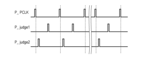
- the pulse signal P_ph which is the output signal of the waveform shaping circuit, is split into a path that is input to the first counter circuit 145 via the first processing circuit 154 and a path that is input to the second counter circuit 146 via the second processing circuit 155.
- a judge signal P_judge1 is input to the first processing circuit 154, and a judge signal P_judge2 is output to the second processing circuit 155.
- the pulse signal P_sig1, which is the output signal of the first processing circuit 154, is input to the output signal processing circuit 147 as OUT1 via the first counter circuit 145.
- the pulse signal P_sig2 which is the output signal of the second processing circuit 155, is input to the output signal processing circuit 147 as OUT2 via the second counter circuit 146.
- the quench element 102 has a switch 112, and the waveform shaping circuit 103 is, for example, an inverter circuit 113.
- the first processing circuit 154 and the second processing circuit 155 may be a first AND circuit 164 and a second AND circuit 165, respectively.
- the first processing circuit 154 and the second processing circuit 155 can be controlled by separate judge signals P_judge.
- the same photon detection signal can be counted simultaneously as outputs with different sensitivities, and more suitable counting information can be output by the output signal processing circuit 147.
- the judge signal P_judge By using two processing circuits and the judge signal P_judge, signal information can be obtained under a greater number of combinations of conditions.
- Fig. 14 is a block diagram showing a schematic configuration of the photoelectric conversion system according to this embodiment.
- the processing device has a control unit 401, a timing adjustment unit 402, an image acquisition unit 403, a readout unit 404, a gain adjustment unit 405, a nonlinear correction unit 406, a defect correction unit 407, a data compression unit 408, and a memory unit 409.
- the image acquisition unit 403 is, for example, the APD 101, and the readout unit 404 is, for example, provided after the counter circuit 105.
- the control unit 401 may be a control unit inside the photoelectric conversion device, or may be outside the photoelectric conversion device.
- the image acquisition unit 403 is controlled by a timing adjustment unit 402 controlled by the control unit 401.
- the image data generated by the image acquisition unit is input to the storage unit 409 after undergoing a correction process. Note that the order of the correction processes is not limited to the order shown in FIG. 14.
- the gain adjustment unit 405 is provided between the readout unit 404 and the nonlinear correction unit 406, and applies a digital gain to the image data generated by the image acquisition unit 403.
- Data for image correction often has decimal values, but if the image output is an integer, the correction accuracy may decrease due to quantization error.
- the effects of quantization error can be suppressed and the correction accuracy can be increased. If the quantization error can be suppressed to 1/4 times or less of the one-photon signal level, the corrected image will be visually natural. For this reason, it is desirable for the digital gain applied to the image data to be, for example, 4 times or more.
- the nonlinear correction unit 406 is disposed between the gain adjustment unit 405 and the scratch correction unit 407, and corrects the image data under the control of the control unit 401.
- the image acquisition unit 403 is a photon-counting type detector
- the optical response often becomes nonlinear due to the effects of dead time.
- overcorrection may occur if correction is performed based on a linear response. Therefore, overcorrection can be prevented by performing nonlinear correction on the image data prior to the calculation processing in the scratch correction unit 407, and appropriate nonlinear correction can be performed according to the drive timing.
- This nonlinear correction is performed using, for example, a LookUpTable.
- the defect correction unit 407 corrects the data of defective pixels contained in the image data. As a specific example, it extracts the output value of the defective pixel and identifies the position information and output value of the defective pixel. There are methods to replace the identified defective pixel with the average value or median value of the outputs of the pixels surrounding the pixel, and methods to divide the estimated defective image data.
- the data compression unit 408 compresses the corrected image data.
- the photoelectric conversion device according to the present invention generates a huge amount of image data corresponding to a high dynamic range.
- the data compression unit 408 the data can be compressed before being stored in the downstream storage unit 409.
- the storage unit 409 is a storage unit that holds at least a portion of the image data generated in the previous stage. Specifically, the image data is stored in a storage unit such as an SRAM, DRAM, or non-volatile memory.
- Fig. 15 is a block diagram showing a schematic configuration of the photoelectric conversion system according to this embodiment.
- the photoelectric conversion device described in the above embodiment can be applied to various photoelectric conversion systems.
- Examples of applicable photoelectric conversion systems include digital still cameras, digital camcorders, surveillance cameras, copiers, fax machines, mobile phones, car-mounted cameras, and observation satellites.
- Camera modules equipped with an optical system such as a lens and an imaging device are also included in photoelectric conversion systems.
- Figure 13 shows a block diagram of a digital still camera as an example of these.
- the photoelectric conversion system illustrated in FIG. 15 includes an image capture device 1004, which is an example of a photoelectric conversion device, and a lens 1002 that forms an optical image of a subject on the image capture device 1004.
- the photoelectric conversion system further includes an aperture 1003 for varying the amount of light passing through the lens 1002, and a barrier 1001 for protecting the lens 1002.
- the lens 1002 and aperture 1003 form an optical system that focuses light on the image capture device 1004.
- the image capture device 1004 is a photoelectric conversion device according to any of the above embodiments, and converts the optical image formed by the lens 1002 into an electrical signal.
- the photoelectric conversion system has a signal processing unit 1007, which is an image generating unit that generates an image by processing an output signal output from the imaging device 1004.
- the signal processing unit 1007 performs various corrections and compression as necessary to output image data.
- the signal processing unit 1007 may be formed in a semiconductor layer in which the imaging device 1004 is provided, or may be formed in a semiconductor layer separate from the imaging device 1004.
- the imaging device 1004 and the signal processing unit 1007 may also be formed in the same semiconductor layer.
- the photoelectric conversion system further has a memory unit 1010 for temporarily storing image data, and an external interface unit (external I/F unit) 1013 for communicating with an external computer or the like.
- the photoelectric conversion system further has a recording medium 1012 such as a semiconductor memory for recording or reading out imaging data, and a recording medium control interface unit (recording medium control I/F unit) 1011 for recording or reading out on the recording medium 1012.
- the recording medium 1012 may be built into the photoelectric conversion system, or may be removable.
- the photoelectric conversion system further includes an overall control/calculation unit 1009 that performs various calculations and controls the entire digital still camera, and a timing generation unit 1008 that outputs various timing signals to the image capture device 1004 and the signal processing unit 1007.
- timing signals and the like may be input from the outside, and the photoelectric conversion system only needs to include at least the image capture device 1004 and the signal processing unit 1007 that processes the output signal output from the image capture device 1004.
- the imaging device 1004 outputs an imaging signal to the signal processing unit 1007.
- the signal processing unit 1007 performs predetermined signal processing on the imaging signal output from the imaging device 1004 and outputs image data.
- the signal processing unit 1007 generates an image using the imaging signal.
- Fig. 16A and Fig. 16B are diagrams showing the configurations of the photoelectric conversion system and the moving object of this embodiment.
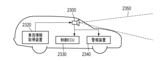
- FIG. 16A shows an example of a photoelectric conversion system for an in-vehicle camera.
- the photoelectric conversion system 2300 has an image capture device 2310.
- the image capture device 2310 is a photoelectric conversion device described in any of the above embodiments.
- the photoelectric conversion system 2300 has an image processing unit 2312 that performs image processing on multiple image data acquired by the image capture device 2310.
- the photoelectric conversion system 2300 also has a parallax acquisition unit 2314 that calculates parallax (phase difference of parallax images) from multiple image data acquired by the photoelectric conversion system 2300.
- the photoelectric conversion system 2300 further has a distance acquisition unit 2316 that calculates the distance to an object based on the calculated parallax, and a collision determination unit 2318 that determines whether or not there is a possibility of a collision based on the calculated distance.
- the parallax acquisition unit 2314 and the distance acquisition unit 2316 are examples of distance information acquisition means that acquire distance information to an object. That is, distance information may be obtained using not only phase difference but also ToF (Time Of Flight) technology.
- the collision determination unit 2318 may use any of these distance information to determine the possibility of a collision.
- the distance information acquisition means may be realized by dedicated hardware or by a software module. It may also be realized by an FPGA (Field Programmable Gate Array), an ASIC (Application Specific Integrated Circuit), or the like, or a combination of these.
- the photoelectric conversion system 2300 is connected to a vehicle information acquisition device 2320, and can acquire vehicle information such as vehicle speed, yaw rate, and steering angle.
- the photoelectric conversion system 2300 is also connected to a control ECU 2330, which is a control device (control unit) that outputs a control signal to generate a braking force for the vehicle based on the judgment result of the collision judgment unit 2318.
- the photoelectric conversion system 2300 is also connected to an alarm device 2340 that issues an alarm to the driver based on the judgment result of the collision judgment unit 2318.
- the control ECU 2330 applies the brakes, releases the accelerator, suppresses engine output, etc., to avoid the collision and reduce damage by controlling the vehicle.
- the alarm device 2340 warns the user by sounding an alarm, displaying alarm information on the screen of a car navigation system, etc., or vibrating the seat belt or steering wheel.
- FIG. 16B shows a photoelectric conversion system for imaging the area in front of the vehicle (imaging range 2350).
- the vehicle information acquisition device 2320 sends instructions to the photoelectric conversion system 2300 or the imaging device 2310. This configuration can further improve the accuracy of distance measurement.
- the photoelectric conversion system is not limited to vehicles such as the vehicle itself, but can be applied to moving bodies (moving devices) such as ships, aircraft, and industrial robots.
- the system can be applied not only to moving bodies, but also to a wide range of equipment that uses object recognition, such as intelligent transport systems (ITS).
- ITS intelligent transport systems
- Fig. 17 is a block diagram showing an example of the configuration of a range image sensor which is the photoelectric conversion system.
- the distance image sensor 1401 is configured to include an optical system 1402, a photoelectric conversion device 1403, an image processing circuit 1404, a monitor 1405, and a memory 1406.
- the distance image sensor 1401 can obtain a distance image according to the distance to the subject by receiving light (modulated light or pulsed light) that is projected from a light source device 1411 toward the subject and reflected by the surface of the subject.
- the optical system 1402 is composed of one or more lenses, and guides image light (incident light) from a subject to the photoelectric conversion device 1403, forming an image on the light receiving surface (sensor section) of the photoelectric conversion device 1403.
- the photoelectric conversion device described in the above embodiment is applied as the photoelectric conversion device 1403, and a distance signal indicating the distance determined from the light receiving signal output from the photoelectric conversion device 1403 is supplied to the image processing circuit 1404.
- the image processing circuit 1404 performs image processing to construct a distance image based on the distance signal supplied from the photoelectric conversion device 1403.
- the distance image (image data) obtained by this image processing is then supplied to the monitor 1405 for display, or supplied to the memory 1406 for storage (recording).
- the distance image sensor 1401 configured in this manner, by applying the photoelectric conversion device described above, it is possible to obtain, for example, a more accurate distance image as the pixel characteristics improve.
- Fig. 18 is a diagram showing an example of a schematic configuration of an endoscopic surgery system which is the photoelectric conversion system of this embodiment.
- an operator (doctor) 1131 is shown using an endoscopic surgery system 1103 to perform surgery on a patient 1132 lying on a patient bed 1133.
- the endoscopic surgery system 1103 is composed of an endoscope 1100, surgical tools 1110, and a cart 1134 on which various devices for endoscopic surgery are mounted.
- the endoscope 1100 is composed of a lens barrel 1101, the tip of which is inserted into the body cavity of the patient 1132 at a predetermined length, and a camera head 1102 connected to the base end of the lens barrel 1101.
- the endoscope 1100 is configured as a so-called rigid scope having a rigid lens barrel 1101, but the endoscope 1100 may also be configured as a so-called flexible scope having a flexible lens barrel.
- the tip of the tube 1101 is provided with an opening into which an objective lens is fitted.
- a light source device 1203 is connected to the endoscope 1100, and light generated by the light source device 1203 is guided to the tip of the tube by a light guide extending inside the tube 1101, and is irradiated via the objective lens towards an object to be observed inside the body cavity of the patient 1132.
- the endoscope 1100 may be a direct-viewing endoscope, an oblique-viewing endoscope, or a side-viewing endoscope.
- An optical system and a photoelectric conversion device are provided inside the camera head 1102, and reflected light (observation light) from the observation object is focused on the photoelectric conversion device by the optical system.
- the observation light is photoelectrically converted by the photoelectric conversion device to generate an electrical signal corresponding to the observation light, i.e., an image signal corresponding to the observation image.
- the photoelectric conversion device may be the photoelectric conversion device described in the above-mentioned embodiment.
- the image signal is sent to the camera control unit (CCU: Camera Control Unit) 1135 as RAW data.
- the CCU 1135 is composed of a CPU (Central Processing Unit), a GPU (Graphics Processing Unit), etc., and controls the overall operation of the endoscope 1100 and the display device 1136. Furthermore, the CCU 1135 receives an image signal from the camera head 1102, and performs various image processing on the image signal, such as development processing (demosaic processing), to display an image based on the image signal.
- a CPU Central Processing Unit
- GPU Graphics Processing Unit
- the display device 1136 under the control of the CCU 1135, displays an image based on the image signal that has been subjected to image processing by the CCU 1135.
- the light source device 1203 is composed of a light source such as an LED (Light Emitting Diode) and supplies the endoscope 1100 with illumination light when photographing the surgical site, etc.
- a light source such as an LED (Light Emitting Diode)
- the input device 1137 is an input interface for the endoscopic surgery system 1103. A user can input various information and instructions to the endoscopic surgery system 1103 via the input device 1137.
- the treatment tool control device 1138 controls the operation of the energy treatment tool 1112 for cauterizing tissue, incising, sealing blood vessels, etc.
- the light source device 1203 that supplies illumination light to the endoscope 1100 when photographing the surgical site can be composed of a white light source composed of, for example, an LED, a laser light source, or a combination of these.
- a white light source composed of, for example, an LED, a laser light source, or a combination of these.
- the white light source is composed of a combination of RGB laser light sources, the output intensity and output timing of each color (each wavelength) can be controlled with high precision, so that the white balance of the captured image can be adjusted in the light source device 1203.
- the light source device 1203 may be controlled to change the intensity of the light it outputs at predetermined time intervals.
- the image sensor of the camera head 1102 may be controlled to acquire images in a time-division manner in synchronization with the timing of the change in the light intensity, and the images may be synthesized to generate an image with a high dynamic range that is free of so-called blackout and whiteout.
- the light source device 1203 may also be configured to supply light of a predetermined wavelength band corresponding to special light observation.
- special light observation for example, the wavelength dependency of light absorption in body tissue is utilized. Specifically, a specific tissue such as blood vessels on the mucosal surface is photographed with high contrast by irradiating light of a narrower band than the light irradiated during normal observation (i.e., white light).
- fluorescent observation may be performed in which an image is obtained by fluorescence generated by irradiating excitation light.
- excitation light is irradiated to body tissue and the fluorescence from the body tissue is observed, or a reagent such as indocyanine green (ICG) is locally injected into the body tissue and excitation light corresponding to the fluorescent wavelength of the reagent is irradiated to the body tissue to obtain a fluorescent image.
- the light source device 1203 may be configured to supply narrow band light and/or excitation light corresponding to such special light observation.
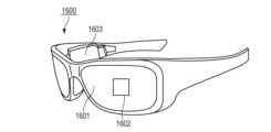
- FIG. 19A is a diagram showing an example of the configuration of glasses 1600 (smart glasses) which are a photoelectric conversion system.
- the glasses 1600 have a photoelectric conversion device 1602.
- the photoelectric conversion device 1602 is the photoelectric conversion device described in the above-mentioned twelfth embodiment.
- a display device including a light-emitting device such as an OLED or an LED may be provided on the back side of the lens 1601.
- the photoelectric conversion device 1602 may be one or more.
- a combination of multiple types of photoelectric conversion devices may be used.
- the arrangement position of the photoelectric conversion device 1602 is not limited to that shown in FIG. 19A.
- the glasses 1600 further include a control device 1603.
- the control device 1603 functions as a power source that supplies power to the photoelectric conversion device 1602 and the display device.
- the control device 1603 also controls the operation of the photoelectric conversion device 1602 and the display device.
- the lens 1601 is formed with an optical system for focusing light on the photoelectric conversion device 1602.
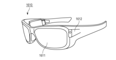
- FIG. 19B illustrates glasses 1610 (smart glasses) according to one application example.
- the glasses 1610 have a control device 1612, which is equipped with a photoelectric conversion device equivalent to the photoelectric conversion device 1602 and a display device.
- the lens 1611 is formed with an optical system for projecting light emitted from the photoelectric conversion device in the control device 1612 and the display device, and an image is projected onto the lens 1611.
- the control device 1612 functions as a power source that supplies power to the photoelectric conversion device and the display device, and controls the operation of the photoelectric conversion device and the display device.
- the control device may have a line of sight detection unit that detects the line of sight of the wearer. Infrared light may be used to detect the line of sight.
- the infrared light emission unit emits infrared light toward the eyeball of a user gazing at a displayed image.
- An imaging unit having a light receiving element detects the reflected light of the emitted infrared light from the eyeball, thereby obtaining an image of the eyeball.
- the user's line of sight with respect to the displayed image is detected from an image of the eyeball obtained by capturing infrared light.
- Any known method can be used for gaze detection using an image of the eyeball.
- a gaze detection method based on the Purkinje image formed by reflection of irradiated light on the cornea can be used.
- gaze detection processing is performed based on the pupil-corneal reflex method.
- a gaze vector that represents the direction (rotation angle) of the eyeball is calculated based on the pupil image and Purkinje image contained in the captured image of the eyeball, thereby detecting the user's gaze.
- the display device of this embodiment may have a photoelectric conversion device having a light receiving element, and may control the display image of the display device based on user line-of-sight information from the photoelectric conversion device.
- the display device determines a first field of view area on which the user gazes and a second field of view area other than the first field of view area based on the line of sight information.
- the first field of view area and the second field of view area may be determined by a control device of the display device, or may be received from an external control device.
- the display resolution of the first field of view area may be controlled to be higher than the display resolution of the second field of view area. In other words, the resolution of the second field of view area may be lower than the first field of view area.
- the display area may have a first display area and a second display area different from the first display area, and an area having a high priority may be determined from the first display area and the second display area based on line-of-sight information.
- the first field of view area and the second field of view area may be determined by a control device of the display device, or may be received from an external control device.
- the resolution of the high priority area may be controlled to be higher than the resolution of areas other than the high priority area. In other words, the resolution of an area having a relatively low priority may be lowered.
- AI may be used to determine the first field of view area and areas with high priority.
- the AI may be a model configured to estimate the angle of gaze and the distance to an object in the line of sight from the image of the eyeball, using as training data an image of the eyeball and the direction in which the eyeball in the image was actually looking.
- the AI program may be possessed by the display device, the photoelectric conversion device, or an external device. If possessed by an external device, it is transmitted to the display device via communication.
- display control is based on visual detection, it is preferably applicable to smart glasses that further include a photoelectric conversion device that captures images of the outside world.
- the smart glasses can display captured external information in real time.
- the disclosure of this embodiment also includes the following configurations and methods.
- a photoelectric conversion device comprising: a photoelectric conversion element that generates a photon detection signal by avalanche multiplication; a circuit that controls a first state in which a first terminal of the photoelectric conversion element is connected to a power supply voltage; and a second state in which a resistance between the first terminal and the power supply voltage is made higher than in the first state; a counter circuit connected to the photoelectric conversion element; and a waveform shaping circuit disposed between the photoelectric conversion element and the counter circuit; and a gating circuit connected between an output node of the waveform shaping circuit and an input node of the counter circuit, for controlling whether or not an output signal of the waveform shaping circuit is input to the counter circuit.
- Configuration 2 The photoelectric conversion device described in configuration 1, characterized in that during one standby state, there is a first period in which the output signal of the waveform shaping circuit is counted, and a second period in which the gating circuit is controlled not to count the output signal of the waveform shaping circuit.
- a pulse generating circuit is provided. 4. The photoelectric conversion device according to any one of configurations 1 to 3, wherein the pulse generating circuit outputs a judgment signal for controlling whether or not the gating circuit counts the output signal of the waveform shaping circuit.
- the gating circuit includes an AND circuit, 6.
- the processing circuit includes a D latch; 9.
- the photoelectric conversion device comprises: a photoelectric conversion element that generates a photon detection signal by avalanche multiplication, a resistive element provided between a first terminal of the photoelectric conversion element and a power supply voltage, and a counter circuit connected to an output node of the photoelectric conversion element.
- a waveform shaping circuit provided between the photoelectric conversion element and the counter circuit, and a gating circuit provided between an output node of the waveform shaping circuit and an input node of the counter circuit for controlling whether or not an output signal of the waveform shaping circuit is input to the counter circuit.
- the photoelectric conversion device comprises: a circuit that counts the number of first periods during which the output signal of the waveform shaping circuit is counted.
- a photoelectric conversion system comprising: the photoelectric conversion device according to any one of configurations 1 to 18; and a signal processing unit that generates an image using a signal output from the photoelectric conversion device.
- (Configuration 20) 19 A moving body including the photoelectric conversion device according to any one of configurations 1 to 18, further comprising a control unit that controls movement of the moving body using a signal output by the photoelectric conversion device.
Landscapes
- Engineering & Computer Science (AREA)
- Multimedia (AREA)
- Signal Processing (AREA)
- Physics & Mathematics (AREA)
- General Physics & Mathematics (AREA)
- Spectroscopy & Molecular Physics (AREA)
- Photometry And Measurement Of Optical Pulse Characteristics (AREA)
- Transforming Light Signals Into Electric Signals (AREA)
Abstract
Description
第1実施形態に係る光電変換装置について図1から図3までを用いて説明する。図1は、光電変換装置の1画素当たりの概略構成図である。図2は、具体的な回路図構成例であり、図3は、図2の回路構成における動作シーケンス図である。
第2実施形態に係る光電変換装置について図4、図5を用いて説明する。第2実施形態に係る光電変換装置は、第1実施形態に係る光電変換装置とは異なるゲーティング回路を用いている。
第3実施形態に係る光電変換装置について図6、図7を用いて説明する。本実施形態に示す光電変換装置では、クエンチ素子102として抵抗素子132が配されている。本実施形態ではクエンチ素子のクロック信号による制御は行われない。いわゆるパッシブリチャージ駆動のSPADを用いた光電変換装置について説明する。
第4実施形態に係る光電変換装置について図8から図10を用いて説明する。本実施形態に係る光電変換装置は2つのカウンタ回路を有し、これらのカウンタ回路が時間的に重複して異なる値の計数を行うことができる。さらに、各カウンタ回路における計数値を処理して、1つの計数値を出力する。
図11から図13では、第5実施形態として上述した第4実施形態の構成の変形例を説明する。図8から図11までに示す構成との差異は各画素が2つの処理回路を有し、処理回路のそれぞれが各カウンタ回路に対応することである。
図14を用いて上述の各実施形態に係る光電変換装置を用いた光電変換システムについて説明する。図14は本実施形態に係る光電変換システムの概略構成を示すブロック図である。
本実施形態による光電変換システムについて、図15を用いて説明する。図15は、本実施形態による光電変換システムの概略構成を示すブロック図である。
本実施形態の光電変換システム及び移動体について、図16A、図16Bを用いて説明する。図16A及び図16Bは、本実施形態の光電変換システム及び移動体の構成を示す図である。
本実施形態の光電変換システムについて、図17を用いて説明する。図17は、光電変換システムである距離画像センサの構成例を示すブロック図である。
本実施形態の光電変換システムについて、図18を用いて説明する。図18は、本実施形態の光電変換システムである内視鏡手術システムの概略的な構成の一例を示す図である。
本実施形態の光電変換システムについて、図19A、図19Bを用いて説明する。図19Aは、光電変換システムである眼鏡1600(スマートグラス)の構成の一例を示す図である。眼鏡1600には、光電変換装置1602を有する。光電変換装置1602は、上記のから第12の実施形態に記載の光電変換装置である。また、レンズ1601の裏面側には、OLEDやLED等の発光装置を含む表示装置が設けられていてもよい。光電変換装置1602は1つでもよいし、複数でもよい。また、複数種類の光電変換装置を組み合わせて用いてもよい。光電変換装置1602の配置位置は図19Aに限定されない。
アバランシェ増倍によって光子検出信号を発生させる光電変換素子と、前記光電変換素子の第1の端子を電源電圧に接続する第1の状態と、前記第1の端子と前記電源電圧との間を前記第1の状態よりも高抵抗にする第2の状態と、を制御する回路を有する。前記光電変換素子に接続されたカウンタ回路と、前記光電変換素子と前記カウンタ回路との間に配された波形整形回路と、を有する。さらに、前記波形整形回路の出力ノードと前記カウンタ回路の入力ノードとの間に接続され、前記波形整形回路の出力信号を前記カウンタ回路に入力するか否かを制御するゲーティング回路を有することを特徴とする光電変換装置。
1回の待機状態中に、前記波形整形回路の出力信号を計数する第1の期間と、前記波形整形回路の出力信号を計数しないよう前記ゲーティング回路が制御された第2の期間と、を有することを特徴とする構成1に記載の光電変換装置。
前記第2の状態は、前記第1の端子と前記電源電圧を接続させないことを特徴とする構成1または2に記載の光電変換装置。
パルス生成回路を有し、
前記パルス生成回路は前記ゲーティング回路が前記波形整形回路の出力信号を計数するか否かを制御するジャッジ信号を出力することを特徴とする構成1から構成3のいずれかに記載の光電変換装置。
前記ゲーティング回路には、前記波形整形回路から出力された信号と前記ジャッジ信号とが入力されることを特徴とする構成4に記載の光電変換装置。
前記カウンタ回路の1回のカウント期間は、前記第2の状態の開始から、前記ジャッジ信号のパルスが前記ゲーティング回路に入力されるまでの期間であることを特徴とする構成5に記載の光電変換装置。
前記ゲーティング回路は、AND回路を含み、
前記AND回路に前記波形整形回路の出力信号と前記ジャッジ信号とが入力されることを特徴とする構成5に記載の光電変換装置。
前記カウンタ回路によるカウントの期間は前記ジャッジ信号のレベルがHighである期間、または前記ジャッジ信号のレベルがLowである期間によって規定されることを特徴とする構成5に記載の光電変換装置。
処理回路は、Dラッチを含み、
前記Dラッチに前記波形整形回路の出力信号と前記ジャッジ信号とが入力されることを特徴とする構成8に記載の光電変換装置。
前記光電変換素子の出力ノードに接続された第2のカウンタ回路を有することを特徴とする構成1から構成9のいずれかに記載の光電変換装置。
単一の前記波形整形回路の出力信号の入力に対し、前記カウンタ回路は第1の計数値を出力し、前記第2のカウンタ回路は第2の計数値を出力する。前記第1の計数値と前記第2の計数値との計数は時間的に重複して行われることを特徴とする構成10に記載の光電変換装置。
前記第1の計数値と、前記第2の計数値と、を処理して1つの計数値を出力する、信号処理回路を有することを特徴とする構成11に記載の光電変換装置。
アバランシェ増倍によって光子検出信号を発生させる光電変換素子と、前記光電変換素子の第1の端子と電源電圧との間に設けられた抵抗素子と、前記光電変換素子の出力ノードに接続されたカウンタ回路と、を有する。前記光電変換素子と前記カウンタ回路との間に配された波形整形回路と、前記波形整形回路の出力ノードと前記カウンタ回路の入力ノードとの間に、前記波形整形回路の出力信号を前記カウンタ回路に入力するか否かを制御するゲーティング回路と、を有する。1回の待機状態中に、前記波形整形回路の出力信号を計数する第1の期間と、前記波形整形回路の出力信号を計数しないよう前記ゲーティング回路が制御された第2の期間がある。前記波形整形回路の出力信号が計数された第1の期間の数をカウントする回路を有することを特徴とする光電変換装置。
前記抵抗素子はクエンチ素子であることを特徴とする構成13に記載の光電変換装置。
パルス生成回路を有し、前記パルス生成回路は前記ゲーティング回路が前記波形整形回路の出力信号を計数するか否かを制御するジャッジ信号を出力することを特徴とする構成14に記載の光電変換装置。
前記ゲーティング回路には、前記波形整形回路から出力された信号と前記ジャッジ信号とが入力されることを特徴とする構成15に記載の光電変換装置。
前記カウンタ回路によるカウントの期間は前記ジャッジ信号のレベルがHighである期間、または前記ジャッジ信号のレベルがLowである期間によって規定されることを特徴とする構成16に記載の光電変換装置。
処理回路は、Dラッチを含み、前記Dラッチに前記波形整形回路の出力信号と前記ジャッジ信号とが入力されることを特徴とする構成17に記載の光電変換装置。
構成1から構成18のいずれか1項に記載の光電変換装置と、前記光電変換装置が出力する信号を用いて画像を生成する信号処理部と、を有することを特徴とする光電変換システム。
構成1から構成18のいずれか1項に記載の光電変換装置を含む移動体であって、前記光電変換装置が出力する信号を用いて前記移動体の移動を制御する制御部を有することを特徴とする移動体。
102 クエンチ素子
105 カウンタ回路
103 波形整形回路
104 処理回路
Claims (20)
- アバランシェ増倍によって光子検出信号を発生させる光電変換素子と、
前記光電変換素子の第1の端子を電源電圧に接続する第1の状態と、前記第1の端子と前記電源電圧との間を前記第1の状態よりも高抵抗にする第2の状態と、を制御する回路と、
前記光電変換素子に接続されたカウンタ回路と、
前記光電変換素子と前記カウンタ回路との間に配された波形整形回路と、
前記波形整形回路の出力ノードと前記カウンタ回路の入力ノードとの間に接続され、前記波形整形回路の出力信号を前記カウンタ回路に入力するか否かを制御するゲーティング回路を有することを特徴とする光電変換装置。 - 1回の待機状態中に、前記波形整形回路の出力信号を計数する第1の期間と、前記波形整形回路の出力信号を計数しないよう前記ゲーティング回路が制御された第2の期間と、
を有することを特徴とする請求項1に記載の光電変換装置。 - 前記第2の状態は、前記第1の端子と前記電源電圧を接続させないことを特徴とする請求項1に記載の光電変換装置。
- パルス生成回路を有し、
前記パルス生成回路は前記ゲーティング回路が前記波形整形回路の出力信号を計数するか否かを制御するジャッジ信号を出力することを特徴とする請求項1に記載の光電変換装置。 - 前記ゲーティング回路には、前記波形整形回路から出力された信号と前記ジャッジ信号とが入力されることを特徴とする請求項4に記載の光電変換装置。
- 前記カウンタ回路の1回のカウント期間は、前記第2の状態の開始から、前記ジャッジ信号のパルスが前記ゲーティング回路に入力されるまでの期間であることを特徴とする請求項5に記載の光電変換装置。
- 前記ゲーティング回路は、AND回路を含み、
前記AND回路に前記波形整形回路の出力信号と前記ジャッジ信号とが入力されることを特徴とする請求項5に記載の光電変換装置。 - 前記カウンタ回路によるカウントの期間は前記ジャッジ信号のレベルがHighである期間、または前記ジャッジ信号のレベルがLowである期間によって規定されることを特徴とする請求項5に記載の光電変換装置。
- 処理回路は、Dラッチを含み、
前記Dラッチに前記波形整形回路の出力信号と前記ジャッジ信号とが入力されることを特徴とする請求項8に記載の光電変換装置。 - 前記光電変換素子の出力ノードに接続された第2のカウンタ回路を有することを特徴とする請求項1に記載の光電変換装置。
- 単一の前記波形整形回路の出力信号の入力に対し、前記カウンタ回路は第1の計数値を出力し、前記第2のカウンタ回路は第2の計数値を出力し、前記第1の計数値と前記第2の計数値との計数は時間的に重複して行われることを特徴とする請求項10に記載の光電変換装置。
- 前記第1の計数値と、前記第2の計数値と、を処理して1つの計数値を出力する、信号処理回路を有することを特徴とする請求項11に記載の光電変換装置。
- アバランシェ増倍によって光子検出信号を発生させる光電変換素子と、
前記光電変換素子の第1の端子と電源電圧との間に設けられた抵抗素子と、
前記光電変換素子の出力ノードに接続されたカウンタ回路と、
前記光電変換素子と前記カウンタ回路との間に配された波形整形回路と、
前記波形整形回路の出力ノードと前記カウンタ回路の入力ノードとの間に、前記波形整形回路の出力信号を前記カウンタ回路に入力するか否かを制御するゲーティング回路と、
を有し、
1回の待機状態中に、前記波形整形回路の出力信号を計数する第1の期間と、前記波形整形回路の出力信号を計数しないよう前記ゲーティング回路が制御された第2の期間があり、
前記波形整形回路の出力信号が計数された第1の期間の数をカウントする回路を有することを特徴とする光電変換装置。 - 前記抵抗素子はクエンチ素子であることを特徴とする請求項13に記載の光電変換装置。
- パルス生成回路を有し、
前記パルス生成回路は前記ゲーティング回路が前記波形整形回路の出力信号を計数するか否かを制御するジャッジ信号を出力することを特徴とする請求項14に記載の光電変換装置。 - 前記ゲーティング回路には、前記波形整形回路から出力された信号と前記ジャッジ信号とが入力されることを特徴とする請求項15に記載の光電変換装置。
- 前記カウンタ回路によるカウントの期間は前記ジャッジ信号のレベルがHighである期間、または前記ジャッジ信号のレベルがLowである期間によって規定されることを特徴とする請求項16に記載の光電変換装置。
- 処理回路は、Dラッチを含み、
前記Dラッチに前記波形整形回路の出力信号と前記ジャッジ信号とが入力されることを特徴とする請求項17に記載の光電変換装置。 - 請求項1乃至請求項18のいずれか1項に記載の光電変換装置と、
前記光電変換装置が出力する信号を用いて画像を生成する信号処理部と、を有することを特徴とする光電変換システム。 - 請求項1乃至請求項18のいずれか1項に記載の光電変換装置を含む移動体であって、
前記光電変換装置が出力する信号を用いて前記移動体の移動を制御する制御部を有することを特徴とする移動体。
Priority Applications (3)
| Application Number | Priority Date | Filing Date | Title |
|---|---|---|---|
| EP24831706.7A EP4738870A1 (en) | 2023-06-30 | 2024-06-14 | Photoelectric conversion device and photoelectric conversion system having said photoelectric conversion device |
| CN202480043220.4A CN121399967A (zh) | 2023-06-30 | 2024-06-14 | 光电转换装置和包括光电转换装置的光电转换系统 |
| US19/411,906 US20260092810A1 (en) | 2023-06-30 | 2025-12-08 | Photoelectric conversion device and photoelectric conversion system including photoelectric conversion device |
Applications Claiming Priority (2)
| Application Number | Priority Date | Filing Date | Title |
|---|---|---|---|
| JP2023108683A JP2025007354A (ja) | 2023-06-30 | 2023-06-30 | 光電変換装置及び該光電変換装置を有する光電変換システム |
| JP2023-108683 | 2023-06-30 |
Related Child Applications (1)
| Application Number | Title | Priority Date | Filing Date |
|---|---|---|---|
| US19/411,906 Continuation US20260092810A1 (en) | 2023-06-30 | 2025-12-08 | Photoelectric conversion device and photoelectric conversion system including photoelectric conversion device |
Publications (1)
| Publication Number | Publication Date |
|---|---|
| WO2025004841A1 true WO2025004841A1 (ja) | 2025-01-02 |
Family
ID=93938912
Family Applications (1)
| Application Number | Title | Priority Date | Filing Date |
|---|---|---|---|
| PCT/JP2024/021596 Ceased WO2025004841A1 (ja) | 2023-06-30 | 2024-06-14 | 光電変換装置及び該光電変換装置を有する光電変換システム |
Country Status (5)
| Country | Link |
|---|---|
| US (1) | US20260092810A1 (ja) |
| EP (1) | EP4738870A1 (ja) |
| JP (1) | JP2025007354A (ja) |
| CN (1) | CN121399967A (ja) |
| WO (1) | WO2025004841A1 (ja) |
Citations (6)
| Publication number | Priority date | Publication date | Assignee | Title |
|---|---|---|---|---|
| JP2020088520A (ja) * | 2018-11-21 | 2020-06-04 | キヤノン株式会社 | 光電変換装置及び撮像システム |
| JP2020123847A (ja) | 2019-01-30 | 2020-08-13 | キヤノン株式会社 | 光電変換装置、撮像システム、移動体 |
| WO2022057831A1 (zh) * | 2020-09-16 | 2022-03-24 | 南京大学 | 基于时间延迟积分(tdi)的图像传感器及其成像方法 |
| JP2022067623A (ja) * | 2020-10-20 | 2022-05-06 | キヤノン株式会社 | 光電変換素子、光電変換素子の制御方法、および情報処理装置。 |
| JP2023061643A (ja) * | 2021-10-20 | 2023-05-02 | キヤノン株式会社 | 光電変換装置 |
| JP2023108683A (ja) | 2022-01-26 | 2023-08-07 | キヤノン株式会社 | 検品システム、印刷装置、検品システムの制御方法 |
-
2023
- 2023-06-30 JP JP2023108683A patent/JP2025007354A/ja active Pending
-
2024
- 2024-06-14 EP EP24831706.7A patent/EP4738870A1/en active Pending
- 2024-06-14 WO PCT/JP2024/021596 patent/WO2025004841A1/ja not_active Ceased
- 2024-06-14 CN CN202480043220.4A patent/CN121399967A/zh active Pending
-
2025
- 2025-12-08 US US19/411,906 patent/US20260092810A1/en active Pending
Patent Citations (6)
| Publication number | Priority date | Publication date | Assignee | Title |
|---|---|---|---|---|
| JP2020088520A (ja) * | 2018-11-21 | 2020-06-04 | キヤノン株式会社 | 光電変換装置及び撮像システム |
| JP2020123847A (ja) | 2019-01-30 | 2020-08-13 | キヤノン株式会社 | 光電変換装置、撮像システム、移動体 |
| WO2022057831A1 (zh) * | 2020-09-16 | 2022-03-24 | 南京大学 | 基于时间延迟积分(tdi)的图像传感器及其成像方法 |
| JP2022067623A (ja) * | 2020-10-20 | 2022-05-06 | キヤノン株式会社 | 光電変換素子、光電変換素子の制御方法、および情報処理装置。 |
| JP2023061643A (ja) * | 2021-10-20 | 2023-05-02 | キヤノン株式会社 | 光電変換装置 |
| JP2023108683A (ja) | 2022-01-26 | 2023-08-07 | キヤノン株式会社 | 検品システム、印刷装置、検品システムの制御方法 |
Also Published As
| Publication number | Publication date |
|---|---|
| EP4738870A1 (en) | 2026-05-06 |
| JP2025007354A (ja) | 2025-01-17 |
| US20260092810A1 (en) | 2026-04-02 |
| CN121399967A (zh) | 2026-01-23 |
Similar Documents
| Publication | Publication Date | Title |
|---|---|---|
| KR102869041B1 (ko) | 광전변환장치 및 광전변환 시스템 | |
| JP7661212B2 (ja) | 光電変換装置、光検出システム | |
| JP2024160505A (ja) | 光電変換装置、光検出システム、移動体および光電変換装置の制御方法 | |
| US11937006B2 (en) | Photoelectric conversion apparatus and photoelectric conversion system | |
| JP7791136B2 (ja) | 光電変換装置 | |
| US12133011B1 (en) | Photoelectric conversion device and photodetection system | |
| JP7516460B2 (ja) | 光電変換装置、光電変換システム | |
| JP2023102966A (ja) | 光電変換装置 | |
| JP7753044B2 (ja) | 光電変換装置 | |
| US20240060819A1 (en) | Photoelectric conversion device, imaging system, light detection system, and mobile body | |
| US11784195B2 (en) | Photoelectric conversion apparatus and photodetection system | |
| US12575221B2 (en) | Apparatus and system | |
| US20250102636A1 (en) | Photoelectric conversion device | |
| JP2025007354A (ja) | 光電変換装置及び該光電変換装置を有する光電変換システム | |
| US20250142231A1 (en) | Device, system, and moving body | |
| US20260110777A1 (en) | Photoelectric conversion device and photoelectric conversion system including photoelectric conversion device | |
| JP2025009968A (ja) | 光電変換装置及び該光電変換装置を有する光電変換システム | |
| WO2025005215A1 (ja) | 光電変換装置及び該光電変換装置を有する光電変換システム | |
| JP2025009969A (ja) | 光電変換装置および光電変換装置を有する光電変換システム | |
| JP2025138051A (ja) | 光電変換装置、光電変換システム、移動体、および機器 | |
| JP2025107036A (ja) | 光電変換装置及び光検出システム | |
| JP2025058595A (ja) | 光電変換装置、光電変換システム、移動体 | |
| JP2025031227A (ja) | 半導体装置 | |
| WO2023131996A1 (ja) | 光電変換装置及び光検出システム |
Legal Events
| Date | Code | Title | Description |
|---|---|---|---|
| 121 | Ep: the epo has been informed by wipo that ep was designated in this application |
Ref document number: 24831706 Country of ref document: EP Kind code of ref document: A1 |
|
| WWE | Wipo information: entry into national phase |
Ref document number: 2024831706 Country of ref document: EP |
|
| NENP | Non-entry into the national phase |
Ref country code: DE |
|
| ENP | Entry into the national phase |
Ref document number: 2024831706 Country of ref document: EP Effective date: 20260130 |
|
| ENP | Entry into the national phase |
Ref document number: 2024831706 Country of ref document: EP Effective date: 20260130 |
|
| WWP | Wipo information: published in national office |
Ref document number: 2024831706 Country of ref document: EP |