WO2025004572A1 - 静電チャック装置 - Google Patents
静電チャック装置 Download PDFInfo
- Publication number
- WO2025004572A1 WO2025004572A1 PCT/JP2024/017785 JP2024017785W WO2025004572A1 WO 2025004572 A1 WO2025004572 A1 WO 2025004572A1 JP 2024017785 W JP2024017785 W JP 2024017785W WO 2025004572 A1 WO2025004572 A1 WO 2025004572A1
- Authority
- WO
- WIPO (PCT)
- Prior art keywords
- electrostatic chuck
- heat conduction
- chuck device
- annular protrusion
- thickness direction
- Prior art date
- Legal status (The legal status is an assumption and is not a legal conclusion. Google has not performed a legal analysis and makes no representation as to the accuracy of the status listed.)
- Ceased
Links
Images





Classifications
-
- H—ELECTRICITY
- H10—SEMICONDUCTOR DEVICES; ELECTRIC SOLID-STATE DEVICES NOT OTHERWISE PROVIDED FOR
- H10P—GENERIC PROCESSES OR APPARATUS FOR THE MANUFACTURE OR TREATMENT OF DEVICES COVERED BY CLASS H10
- H10P72/00—Handling or holding of wafers, substrates or devices during manufacture or treatment thereof
- H10P72/70—Handling or holding of wafers, substrates or devices during manufacture or treatment thereof for supporting or gripping
- H10P72/72—Handling or holding of wafers, substrates or devices during manufacture or treatment thereof for supporting or gripping using electrostatic chucks
- H10P72/722—Details of electrostatic chucks
-
- H—ELECTRICITY
- H01—ELECTRIC ELEMENTS
- H01J—ELECTRIC DISCHARGE TUBES OR DISCHARGE LAMPS
- H01J37/00—Discharge tubes with provision for introducing objects or material to be exposed to the discharge, e.g. for the purpose of examination or processing thereof
- H01J37/32—Gas-filled discharge tubes
- H01J37/32431—Constructional details of the reactor
- H01J37/32715—Workpiece holder
- H01J37/32724—Temperature
-
- H—ELECTRICITY
- H02—GENERATION; CONVERSION OR DISTRIBUTION OF ELECTRIC POWER
- H02N—ELECTRIC MACHINES NOT OTHERWISE PROVIDED FOR
- H02N13/00—Clutches or holding devices using electrostatic attraction, e.g. using Johnson-Rahbek effect
-
- H—ELECTRICITY
- H10—SEMICONDUCTOR DEVICES; ELECTRIC SOLID-STATE DEVICES NOT OTHERWISE PROVIDED FOR
- H10P—GENERIC PROCESSES OR APPARATUS FOR THE MANUFACTURE OR TREATMENT OF DEVICES COVERED BY CLASS H10
- H10P72/00—Handling or holding of wafers, substrates or devices during manufacture or treatment thereof
- H10P72/04—Apparatus for manufacture or treatment
- H10P72/0431—Apparatus for thermal treatment
- H10P72/0434—Apparatus for thermal treatment mainly by convection
-
- H—ELECTRICITY
- H10—SEMICONDUCTOR DEVICES; ELECTRIC SOLID-STATE DEVICES NOT OTHERWISE PROVIDED FOR
- H10P—GENERIC PROCESSES OR APPARATUS FOR THE MANUFACTURE OR TREATMENT OF DEVICES COVERED BY CLASS H10
- H10P72/00—Handling or holding of wafers, substrates or devices during manufacture or treatment thereof
- H10P72/70—Handling or holding of wafers, substrates or devices during manufacture or treatment thereof for supporting or gripping
-
- H—ELECTRICITY
- H10—SEMICONDUCTOR DEVICES; ELECTRIC SOLID-STATE DEVICES NOT OTHERWISE PROVIDED FOR
- H10P—GENERIC PROCESSES OR APPARATUS FOR THE MANUFACTURE OR TREATMENT OF DEVICES COVERED BY CLASS H10
- H10P72/00—Handling or holding of wafers, substrates or devices during manufacture or treatment thereof
- H10P72/70—Handling or holding of wafers, substrates or devices during manufacture or treatment thereof for supporting or gripping
- H10P72/76—Handling or holding of wafers, substrates or devices during manufacture or treatment thereof for supporting or gripping using mechanical means, e.g. clamps or pinches
- H10P72/7604—Handling or holding of wafers, substrates or devices during manufacture or treatment thereof for supporting or gripping using mechanical means, e.g. clamps or pinches the wafers being placed on a susceptor, stage or support
- H10P72/7616—Handling or holding of wafers, substrates or devices during manufacture or treatment thereof for supporting or gripping using mechanical means, e.g. clamps or pinches the wafers being placed on a susceptor, stage or support characterised by a coating, a hardness or a material
-
- H—ELECTRICITY
- H10—SEMICONDUCTOR DEVICES; ELECTRIC SOLID-STATE DEVICES NOT OTHERWISE PROVIDED FOR
- H10P—GENERIC PROCESSES OR APPARATUS FOR THE MANUFACTURE OR TREATMENT OF DEVICES COVERED BY CLASS H10
- H10P72/00—Handling or holding of wafers, substrates or devices during manufacture or treatment thereof
- H10P72/70—Handling or holding of wafers, substrates or devices during manufacture or treatment thereof for supporting or gripping
- H10P72/76—Handling or holding of wafers, substrates or devices during manufacture or treatment thereof for supporting or gripping using mechanical means, e.g. clamps or pinches
- H10P72/7604—Handling or holding of wafers, substrates or devices during manufacture or treatment thereof for supporting or gripping using mechanical means, e.g. clamps or pinches the wafers being placed on a susceptor, stage or support
- H10P72/7624—Handling or holding of wafers, substrates or devices during manufacture or treatment thereof for supporting or gripping using mechanical means, e.g. clamps or pinches the wafers being placed on a susceptor, stage or support characterised by the mechanical construction of the susceptor, stage or support
Definitions
- One of the objectives of the present invention is to provide an electrostatic chuck device that can suppress distortion of the annular convex portion during substrate processing and suppress gas leakage from between the substrate and the annular convex portion.
- An electrostatic chuck device comprising: a dielectric substrate having a mounting surface on which a plate-shaped sample is placed; an electrostatic chuck unit having an adsorption electrode disposed inside the dielectric substrate; and a base supporting the electrostatic chuck unit from a back surface side opposite to the mounting surface and capable of adjusting a temperature of the electrostatic chuck unit, wherein the electrostatic chuck unit has an annular convex portion that protrudes upward from an outer periphery of an upper surface of the dielectric substrate and is formed in a ring shape when viewed in a thickness direction of the electrostatic chuck unit, the base having a mounting surface on which the electrostatic chuck unit is mounted, and a heat conduction suppression unit provided on the mounting surface, and at least a portion of the heat conduction suppression unit is located radially inward of the annular convex portion when viewed in the thickness direction.
- a radial width d of a portion where the annular protrusion and a part of the heat conduction suppressing portion overlap with each other is, relative to a radial width L of the annular protrusion, 0 ⁇ d ⁇ L/2
- the electrostatic chuck device according to [3], [5] The electrostatic chuck device according to any one of [1] to [4], wherein the thermal conductivity of the heat conduction suppressing portion is lower than the thermal conductivity of the base.
- the heat conduction suppression portion is provided in plurality at intervals between each other in a circumferential direction about a central axis of the electrostatic chuck portion.
- the above aspect of the present invention provides an electrostatic chuck device that can suppress distortion of the annular protrusion during substrate processing and suppress gas leakage from between the substrate and the annular protrusion.
- FIG. 1 is a schematic cross-sectional view illustrating an example of an electrostatic chuck device according to a first embodiment.
- FIG. 2 is a schematic cross-sectional view showing an enlarged portion of the electrostatic chuck device shown in FIG.
- FIG. 3 is a schematic cross-sectional plan view showing an example of the configuration of a heat conduction suppression portion of an electrostatic chuck device.
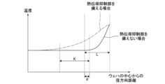
- FIG. 4 is a diagram showing an example of temperature distribution at the outer periphery of a wafer held by an electrostatic chuck device with and without a heat conduction suppressing portion.
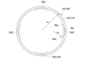
- FIG. 5 is a schematic cross-sectional plan view showing an example of the configuration of a heat conduction suppressing portion in an electrostatic chuck device according to the second embodiment.
- FIG. 1 is a schematic cross-sectional view illustrating an example of an electrostatic chuck device according to a first embodiment.
- FIG. 2 is a schematic cross-sectional view showing an enlarged portion of the electrostatic chuck device shown in FIG.
- FIG. 3
- FIG. 6 is a schematic cross-sectional plan view showing an example of the configuration of a heat conduction suppressing portion in an electrostatic chuck device according to the third embodiment.
- FIG. 7 is a schematic cross-sectional plan view showing an example of the configuration of a heat conduction suppressing portion in an electrostatic chuck device according to the fourth embodiment.
- FIG. 8 is a schematic explanatory diagram showing an example of a semiconductor manufacturing apparatus having the electrostatic chuck device described above.
- FIG. 1 is a schematic cross-sectional view showing an example of an electrostatic chuck device according to the present embodiment.
- the electrostatic chuck device 100 shown in FIG. 1 is disposed in a vacuum chamber of a plasma processing device with, for example, a mounting surface 11a on which a wafer (plate-shaped sample) W is placed facing upward.
- a Z-axis is shown to explain the reference of the electrostatic chuck device.
- the Z-axis direction is, for example, a vertical direction.
- the central axis O of the mounting surface 11a is parallel to the Z-axis.
- the arrangement of the electrostatic chuck device 100 with respect to the vertical direction is an example, and other arrangements may be used.
- the electrostatic chuck device 100 includes an electrostatic chuck unit 10 that adsorbs and supports a plate-shaped sample such as a wafer W, a base 20 that supports the electrostatic chuck unit 10, and a heat conduction suppression unit 50A.
- the electrostatic chuck unit 10 includes a dielectric substrate 11 and an adsorption electrode 30 .
- the dielectric substrate 11 is a plate-like member that is circular or approximately circular in plan view.
- the thickness direction of the dielectric substrate 11 may be simply referred to as the "thickness direction”.
- the electrostatic chuck device will be described with the side in the thickness direction on which the wafer W is mounted being referred to as the "upper side” and the opposite side being referred to as the "lower side”.
- the "upper side” and the “lower side” indicate examples of the posture of the electrostatic chuck device when in use, and do not limit the posture of the electrostatic chuck device when in use.
- the dielectric substrate 11 is preferably made of a composite sintered body that has mechanical strength and is resistant to corrosive gases and their plasma.
- the dielectric material that constitutes the dielectric substrate 11 ceramics that have mechanical strength and are resistant to corrosive gases and their plasma are preferably used.
- the ceramics that constitute the dielectric substrate 11 for example, aluminum oxide sintered body, aluminum nitride sintered body, aluminum oxide-silicon carbide composite sintered body, etc. are preferably used.
- the upper surface of the dielectric substrate 11 is provided with a mounting surface 11a on which the wafer W is placed. That is, the dielectric substrate 11 is provided with a mounting surface 11a on which the wafer W is placed.
- a plurality of protrusions 12 protruding upward are formed at predetermined intervals on the upper surface of the dielectric substrate 11.
- FIG. 2 is an enlarged cross-sectional view of a portion of the electrostatic chuck device of FIG.
- the protrusions 12 located on the outer periphery of the dielectric substrate 11 are annular convex portions 12C formed in a ring shape when viewed from the thickness direction.
- the annular convex portion is preferably continuous, and its upper surface is preferably flat.
- the ring shape may mean a circular ring shape or a substantially circular ring shape.
- the annular protrusion 12C and the dielectric substrate 11 are preferably integrally formed, and the annular protrusion 12C and the dielectric substrate 11 are preferably formed from the same material, but are not limited to these examples. As shown in FIG.
- the annular protrusion 12C has a width L of, for example, 0.5 mm to 5 mm, which is arbitrarily selected in the radial direction of the dielectric substrate 11.
- the width L may be 0.8 mm to 3.5 mm, 1.5 mm to 2.5 mm, or the like.
- the tip surface (mounting surface 11a) of the annular protrusion 12C contacts the underside of the wafer W continuously around the entire circumferential direction of the wafer W. It is preferable that the heights of the annular protrusion 12C and the protrusions 12 are the same or approximately the same.
- recesses (valleys) 13 that are recessed downward from the mounting surface 11a are formed.
- the bottom surface 13b of the recess 13 faces upward (towards the wafer W).
- the dielectric substrate 11 is preferably provided with a gas hole (not shown).
- the gas hole penetrates the dielectric substrate 11 in the thickness direction.
- the gas hole is provided radially inward with respect to the annular protrusion 12C.
- the gas hole is connected to a gas supply device (not shown).
- the gas hole supplies an arbitrarily selected cooling gas, such as helium (He), to the space between the wafer W placed on the mounting surface 11a and the bottom surface 13b of the recess 13.
- the supplied cooling gas cools the wafer W placed on the mounting surface 11a.
- the tip surface of the annular protrusion 12C is in continuous contact with the entire circumference of the underside of the wafer W, thereby preventing the cooling gas from leaking radially outward from the annular protrusion 12C.
- the chucking electrode 30 is embedded in the dielectric substrate 11.
- the chucking electrode 30 is conductive.
- the chucking electrode 30 is located inside the dielectric substrate 11.
- the chucking electrode 30 extends, for example, in a layer shape along a plane perpendicular to the thickness direction of the dielectric substrate 11.
- the chucking electrode 30 is disposed in the dielectric substrate 11 below the mounting surface 11a and the bottom surface 13b, at a predetermined distance therefrom.
- the chucking electrode 30 is connected to a DC power supply (not shown) via a power supply unit (not shown).
- the chucking electrode 30 generates an electrostatic chucking force by a DC current supplied from the DC power supply, and chucking the wafer W to the mounting surface 11a.
- the chucking electrodes 30 may have any shape or number that can be selected.
- the chucking electrodes 30 are not limited to a monopolar chucking electrode, and may be a bipolar chucking electrode consisting of two electrodes that are semicircular in plan view.
- the chucking electrodes 30 may be provided only on a portion of the circumference of the electrostatic chuck unit 10 when viewed from the thickness direction.
- the chucking electrodes 30 may be provided in multiple locations spaced apart from one another in the circumference of the electrostatic chuck unit 10 when viewed from the thickness direction.
- the chucking electrode 30 can be formed of any material, and is, for example, composed of a composite of an insulating material and a conductive material.
- the insulating material contained in this composite is not particularly limited, but is preferably at least one selected from the group consisting of aluminum oxide (Al 2 O 3 ), aluminum nitride (AlN), silicon nitride (Si 3 N 4 ), yttrium (III) oxide (Y 2 O 3 ), yttrium aluminum garnet (YAG) and SmAlO 3.
- the conductive material contained in the composite is preferably at least one selected from the group consisting of molybdenum carbide (Mo 2 C), molybdenum (Mo), tungsten carbide (WC), tungsten (W), tantalum carbide (TaC), tantalum (Ta), silicon carbide (SiC), carbon black, carbon nanotubes and carbon nanofibers.
- the suction electrode 30 may be formed in advance into a predetermined shape, or may be formed by three-dimensional printing, deposition, or the like.
- the suction electrode 30 may be embedded in the dielectric substrate 11 by laminating the dielectric substrate 11 in multiple steps.
- the base 20 of this embodiment is made of a thick disk-shaped metal member.
- the base 20 supports the electrostatic chuck unit 10 from the lower side (the side opposite to the mounting surface 11a).
- the material constituting the base 20 can be selected arbitrarily, and for example, any metal having excellent thermal conductivity, electrical conductivity, and workability, or a composite material containing these metals, can be used without any particular limitation.
- aluminum, aluminum alloy, copper, copper alloy, stainless steel, etc. are preferably used.
- the characteristics and configuration of the base for making the temperature of the electrostatic chuck unit adjustable can be selected arbitrarily. For example, the temperature of the electrostatic chuck unit can be effectively adjusted by the heat conduction suppression unit described below and the flow path described below.
- the base 20 of this embodiment preferably has a flow path 21 for circulating a liquid coolant such as water inside the disk-shaped structure, and in this embodiment, it is water-cooled.
- the coolant circulated in the flow path 21 can be selected arbitrarily, and may be a gas such as He gas or N2 gas.
- Such a base 20 is capable of cooling the electrostatic chuck portion 10 by a coolant circulated through the flow passage 21, and adjusting the temperature thereof.
- the base 20 has a mounting surface 20t facing upward.
- the mounting surface 20t of the base 20 is adhered to the lower surface 11b of the dielectric substrate 11 via an adhesive layer 25.
- the material forming the adhesive layer 25 can be selected arbitrarily, and may be, for example, a heat-resistant resin such as polyimide resin, silicone resin, or epoxy resin, or an insulating sheet- or film-shaped adhesive resin.
- the heat conduction suppression part 50A in this embodiment is embedded in the base 20.
- the heat conduction suppression part 50A is preferably disposed in a recess 22 formed in the mounting surface 20t of the base 20.
- the recess 22 is filled with a selected material or is left as a space.
- the heat conduction suppression part 50A is provided on the mounting surface 20t.
- the upper surface 50a of the heat conduction suppression part 50A in this embodiment is formed at the same height as the mounting surface 20t of the base 20.
- the heat conduction suppression part 50A may be disposed in a hole (a bottomed hole or a through hole) formed in the base 20. For example, it may be provided in the hole.
- FIG. 3 is a cross-sectional plan view showing the configuration of a heat conduction suppressing portion of the electrostatic chuck device.
- the heat conduction suppression part 50A is annular when viewed from the thickness direction. When viewed from the thickness direction, at least a part of the heat conduction suppression part 50A is located radially inward from the annular protrusion 12C.
- the outer peripheral edge 50s of the heat conduction suppression part 50A is located between the inner peripheral edge 12s and the outer peripheral edge 12t of the annular protrusion 12C when viewed from the thickness direction.
- the inner peripheral edge 50t of the heat conduction suppression part 50A is located radially inward from the inner peripheral edge 12s of the annular protrusion 12C when viewed from the thickness direction.
- a radial part of the heat conduction suppression part 50A overlaps with the annular protrusion 12C.
- the outer peripheral edge 50s of the heat conduction suppression portion 50A may be located radially inward of the inner peripheral edge 12s of the annular convex portion 12C when viewed from the thickness direction. In other words, when viewed from the thickness direction, the heat conduction suppression portion 50A may not overlap the annular convex portion 12C, and a radial gap may be formed between the outer peripheral edge 50s of the heat conduction suppression portion 50A and the inner peripheral edge 12s of the annular convex portion 12C.
- the distance between the heat conduction suppression portion 50A and the inner peripheral edge 12s of the annular convex portion 12C can be selected arbitrarily, and may be, for example, 0 to 0.5 times, 0.01 to 0.7 times, 0.05 to 0.8 times, or 0.1 to 1.0 times the radial width of the annular convex portion 12C, but is not limited to these examples.
- the radial width K of the heat conduction suppression portion 50A is preferably larger than the radial width L of the annular convex portion 12C in order to effectively reduce the temperature gradient of the annular convex portion 12C, and is preferably smaller than the thickness of the cooling base 20 in order not to excessively suppress the cooling effect of the wafer.
- the radial width K of the heat conduction suppression portion 50A can be selected arbitrarily, but is preferably set to, for example, 0.5 mm or more and 30 mm or less.
- the width K may be 1.5 mm or more and 25 mm or less, 3.0 mm or more and 20 mm or less, 7.0 mm or more and 15 mm or less, etc.
- the depth (thickness) of the heat conduction suppression portion 50A can be selected arbitrarily, and may be, for example, 0.1 to 1.0 mm, 0.5 to 3.0 mm, or 1.0 to 10.0 mm, but is not limited to these examples.
- the width K is constant, but if the width is not constant, it may mean the value at the position where the radial width is the largest.
- the radial width d of the portion where the annular protrusion 12C and a part of the heat conduction suppressing portion 50A overlap is, relative to the radial width L of the annular protrusion 12C, 0 ⁇ d ⁇ L/2
- Such a setting is more preferable because it is possible to prevent the temperature gradient of the annular protrusion 12C from becoming steep while cooling the outermost periphery of the wafer, which is prone to becoming hot.
- the thermal conductivity of the thermal conduction suppression portion 50A is preferably lower than that of the base 20.
- the thermal conduction suppression portion 50A is preferably formed from a material having a lower thermal conductivity than the material forming the base 20, such as a metal or a composite material containing a metal.
- materials forming the thermal conduction suppression portion 50A include Teflon (registered trademark), plastic materials, organic and inorganic adhesives, insulators with high insulating properties, and ceramic materials. More specific preferred examples include alumina, yttria, and aluminum nitride.
- the thermal conduction suppression portion 50A may be, for example, a space.
- the thermal conductivity of the material forming the thermal conduction suppression unit 50A may be, for example, 0.1 to 10 W/(m ⁇ K), 0.5 to 20 W/(m ⁇ K), 1.0 to 30 W/(m ⁇ K), 5 to 50 W/(m ⁇ K), 10 to 100 W/(m ⁇ K), 100 to 150 W/(m ⁇ K), or 150 to 200 W/(m ⁇ K), but is not limited to these examples.
- the ratio of the thermal conductivity of the thermal conduction suppression unit 50A to the thermal conductivity of the base 20 can be selected arbitrarily, and may be, for example, 0.01 to 0.1 times, 0.05 to 0.5 times, or 0.1 to 0.9 times, but is not limited to these examples.
- FIG. 4 is a diagram showing an example of temperature distribution at the outer periphery of a wafer held by an electrostatic chuck device with and without a heat conduction suppressing portion.
- the temperature distribution at and near the annular convex portion 12C on the outer periphery of the electrostatic chuck portion 10 when performing plasma processing on a wafer W held by the electrostatic chuck portion 10 is compared between a case where the thermal conduction suppression portion 50A is provided and a case where the thermal conduction suppression portion 50A is not provided. As shown in FIG.
- the thermal conduction suppression portion 50A when the thermal conduction suppression portion 50A is not provided, the temperature of the wafer W at the outer periphery of the wafer W in contact with the annular protrusion 12C increases sharply as the temperature moves radially outward of the wafer W, compared to the central portion of the wafer W.
- the heat conduction suppression portion 50A when the heat conduction suppression portion 50A is provided on the mounting surface 20t of the base 20 as in the above embodiment, the temperature of the wafer W rises at the outer periphery of the wafer W in contact with the annular convex portion 12C compared to the central portion of the wafer W, but the temperature gradient, i.e., the temperature rise, is gentle even toward the radially outer side of the wafer W.
- the heat conduction suppression portion 50A suppresses the conduction of the heat (cold heat) that cools the electrostatic chuck portion 10 provided by the refrigerant circulated through the flow passage 21 of the base 20 to the annular convex portion 12C of the electrostatic chuck portion 10 and its vicinity.
- the electrostatic chuck device 100 of this embodiment includes a heat conduction suppression portion 50A, at least a portion of which is located radially inward of the annular protrusion 12C when viewed in the thickness direction.
- This configuration can suppress heat conduction to the annular protrusion 12C of the electrostatic chuck portion 10 and its vicinity. This can reduce distortion that occurs in the annular protrusion 12C when performing plasma processing on the wafer W. As a result, leakage of cooling gas such as helium (He) to the outside from between the wafer W and the annular protrusion 12C is suppressed.
- the radial width K of the heat conduction suppression unit 50A is larger than the radial width L of the annular protrusion 12C.
- the radial width L of the annular protrusion 12C smaller than the radial width K of the heat conduction suppression unit 50A, that is, by making it smaller, the product yield of the wafer W can be increased.
- the radial width K of the heat conduction suppression unit 50A may be 1.0 to 10 times the radial width L of the annular protrusion 12C, more preferably 1.5 to 9 times, even more preferably 2 to 8 times, and particularly preferably 4 to 7 times, but is not limited to these examples. It may be 1.1 to 1.5 times, 1.3 to 1.8 times, etc.
- the annular protrusion 12C and a portion of the heat conduction suppression portion 50A overlap when viewed from the thickness direction. With this configuration, heat conduction from the gap between the annular protrusion 12C and the heat conduction suppression portion 50A is suppressed. This makes it possible to effectively suppress heat conduction to the vicinity of the annular protrusion 12C of the electrostatic chuck portion 10.
- the radial width d of the portion where the annular protrusion 12C and a portion of the heat conduction suppression portion 50A overlap preferably satisfies the relationship 0 ⁇ d ⁇ L/2 with respect to the radial width L of the annular protrusion 12C. It may also be 0 ⁇ d ⁇ L/3, 0 ⁇ d ⁇ L/4, or 0 ⁇ d ⁇ L/6. With this configuration, the width d of the portion where the annular protrusion 12C and a portion of the heat conduction suppression portion 50A overlap can be kept small while effectively suppressing heat conduction to the vicinity of the annular protrusion 12C of the electrostatic chuck portion 10.
- d is selected as necessary, and may be, for example, 0.01 mm to 5.0 mm, 0.05 mm to 2.5 mm, 0.1 mm to 2.0 mm, 0.3 mm to 1.5 mm, or 0.5 mm to 1.0 mm, but is not limited to these examples.
- the width d is constant, but if the width is not constant, it may mean the value at the position where the radial width is the largest.
- the thermal conductivity of the heat conduction suppression portion 50A is lower than the thermal conductivity of the base 20.
- the heat conduction suppression unit 50A is disposed in a recess 22 or hole formed in the mounting surface 20t of the base 20. With this configuration, the heat conduction suppression unit 50A can be easily provided while being integrated with the base 20.
- FIG. 5 is a plan cross-sectional view showing the configuration of a heat conduction suppression unit in an electrostatic chuck device according to a second embodiment.
- the electrostatic chuck device 100 includes an electrostatic chuck unit 10 and a base 20 (not shown).
- a heat conduction suppression unit 50B is provided on a mounting surface 20t of the base 20 (not shown).
- a plurality of heat conduction suppressing portions 50B are provided at equal intervals between each other in the circumferential direction around the central axis of the electrostatic chuck portion 10 as viewed from the thickness direction.
- Each of the plurality of heat conduction suppressing portions 50B has an arc shape formed concentrically with the annular protrusion 12C.
- at least a portion of each heat conduction suppressing portion 50B is located radially inward of the annular protrusion 12C.
- a radial portion of the heat conduction suppressing portion 50B overlaps with the annular protrusion 12C.
- each of the heat conduction suppressing parts 50B has a constant or almost constant width, for example, a radial width, as viewed from the thickness direction.
- Each of the heat conduction suppressing parts 50B is formed only of curved surfaces without corners as viewed from the thickness direction. However, as necessary, it may have corners, for example, a sector shape.
- the number of the heat conduction suppressing parts 50B can be selected arbitrarily, and may be an even number or an odd number. Examples include 2 to 200, 3 to 100, 4 to 50, 6 to 30, 8 to 15, and 10 to 12, but are not limited to these examples.
- the shapes and sizes of the heat conduction suppressing parts 50B are all the same or almost the same as viewed from the thickness direction, but they may have different shapes and sizes as necessary.
- two or more of the shapes of the heat conduction suppressing parts of the second to fourth embodiments may be selected and arranged in combination with each other. Examples include a combination of the heat conduction suppressing parts of the second and third embodiments, a combination of the heat conduction suppressing parts of the third and fourth embodiments, and a combination of the heat conduction suppressing parts of the second and fourth embodiments.
- the thermal conduction suppressing parts 50B are preferably arranged in a balanced manner with regularity.
- the thermal conduction suppressing parts 50B having different shapes may be arranged alternately with gaps between them in the circumferential direction.
- the electrostatic chuck device 100 of this embodiment includes a heat conduction suppression portion 50B, at least a portion of which is located radially inward of the annular protrusion 12C when viewed in the thickness direction.
- This configuration can suppress heat conduction to the vicinity of the annular protrusion 12C of the electrostatic chuck portion 10. This can reduce distortion that occurs in the annular protrusion 12C when performing plasma processing on the wafer W. As a result, leakage of cooling gas such as helium (He) to the outside from between the wafer W and the annular protrusion 12C is suppressed.
- a plurality of heat conduction suppressing portions 50B are provided at intervals between each other in the circumferential direction about the central axis of the electrostatic chuck unit 10. This reduces the suppression of heat conduction between heat conduction suppressing portions 50B adjacent to each other in the circumferential direction. Therefore, the heat conduction suppressing portions 50B can reduce the area of the region where heat conduction to the annular protrusion 12C of the electrostatic chuck unit 10 and its vicinity is suppressed, that is, the area can be reduced.
- the distortion occurring in the annular convex portion 12C is alleviated, but the electrostatic chuck portion 10 may not be sufficiently cooled in the vicinity of the annular convex portion 12C, which may adversely affect the plasma processing of the wafer W.
- the heat conduction suppression portions 50B at intervals in the circumferential direction, it is possible to reduce the area in the vicinity of the annular convex portion 12C where the electrostatic chuck portion 10 cannot be sufficiently cooled. As a result, it is possible to suppress the area in which the plasma processing of the wafer W is adversely affected, and to increase the product yield.
- the heat conduction suppression portion 50B is an arc formed concentrically with the annular protrusion 12C. This makes it easy to form the heat conduction suppression portion 50B.
- the electrostatic chuck device 100 of this embodiment differs from the electrostatic chuck device 100 of the first and second embodiments in the configuration of a heat conduction suppression unit 50C, but has other configurations in common with the electrostatic chuck device 100. Therefore, the following mainly describes the heat conduction suppression unit 50C, and a description of the configurations in common with the electrostatic chuck device 100 will be omitted.
- FIG. 6 is a plan cross-sectional view showing the configuration of a heat conduction suppression unit in an electrostatic chuck device according to a third embodiment.
- the electrostatic chuck device 100 includes an electrostatic chuck unit 10 and a base 20 (not shown).
- a heat conduction suppression unit 50C is provided on the mounting surface 20t of the base 20 (not shown).
- the thermal conduction suppression portions 50C are provided at intervals between each other in the circumferential direction around the central axis of the electrostatic chuck portion 10 when viewed from the thickness direction.
- Each of the thermal conduction suppression portions 50C is an arc shape in which the radius of curvature R2 of the thermal conduction suppression portion 50C is smaller than the radius of curvature R1 of the annular protrusion 12C.
- the central portion 50r of each thermal conduction suppression portion 50C overlaps with the annular protrusion 12C.
- both end portions 50p, 50q of each thermal conduction suppression portion 50C are located radially inward of the annular protrusion 12C.
- the electrostatic chuck device 100 of this embodiment includes a heat conduction suppression portion 50C, at least a portion of which is located radially inward of the annular protrusion 12C when viewed in the thickness direction.
- This configuration can suppress heat conduction to the annular protrusion 12C of the electrostatic chuck portion 10 and its vicinity. This can reduce distortion that occurs in the annular protrusion 12C when performing plasma processing on the wafer W. As a result, leakage of cooling gas such as helium (He) to the outside from between the wafer W and the annular protrusion 12C is suppressed.
- the heat conduction suppression parts 50C are provided in a plurality of positions spaced apart from each other in the circumferential direction around the central axis of the electrostatic chuck part 10. This makes it possible to suppress the area of the region in which heat conduction to the annular protrusion 12C of the electrostatic chuck part 10 and its vicinity is suppressed by the heat conduction suppression parts 50C, i.e., to reduce the area. Therefore, similar to the second embodiment described above, it is possible to reduce the area in the annular protrusion 12C and its vicinity where the electrostatic chuck part 10 cannot be sufficiently cooled. As a result, it is possible to suppress the area that adversely affects the plasma processing of the wafer W, and to increase the product yield.
- the heat conduction suppression portion 50C is an arc shape in which the radius of curvature R2 of the heat conduction suppression portion 50C is smaller than the radius of curvature R1 of the annular convex portion 12C.
- both end portions 50p, 50q of each heat conduction suppression portion 50C are located radially inward of the annular convex portion 12C with respect to the central portion 50r. The effect and position of each heat conduction suppression portion 50C gradually change from the central portion 50r toward the both end portions 50p, 50q.
- the ratio of the radius of curvature R2 of the heat conduction suppression portion 50C to the radius of curvature R1 of the annular convex portion 12C can be selected arbitrarily, and for example, the ratio (R2/R1) can be 1/1 to 1/1.5, 1/1.5 to 1/5, 1/5 to 1/10, or 1/10 to 1/20, but is not limited to these examples.
- an electrostatic chuck device according to a fourth embodiment of the present invention will be described.
- the configuration of the heat conduction suppression unit 50D is different from that of the electrostatic chuck device 100 in the first to third embodiments, but the other configuration is common to the electrostatic chuck device 100. Therefore, the following mainly describes the heat conduction suppression unit 50D, and a description of the configuration common to the electrostatic chuck device 100 will be omitted.
- FIG. 7 is a plan cross-sectional view showing the configuration of a heat conduction suppression unit in an electrostatic chuck device according to a fourth embodiment.
- the electrostatic chuck device 100 includes an electrostatic chuck unit 10 and a base 20 (not shown).
- a heat conduction suppression unit 50D is provided on the mounting surface 20t of the base 20 (not shown).
- the heat conduction suppression portions 50D are provided at intervals in the circumferential direction around the central axis of the electrostatic chuck portion 10 when viewed from the thickness direction.
- each of the heat conduction suppression portions 50D is circular and has a radius R3 that is smaller than the radius of curvature R1 of the annular protrusion 12C.
- a portion of each heat conduction suppression portion 50D overlaps with the annular protrusion 12C, and the remaining portion is located radially inward of the annular protrusion 12C.
- the electrostatic chuck device 100 of this embodiment includes a heat conduction suppression portion 50D, at least a portion of which is located radially inward of the annular protrusion 12C when viewed in the thickness direction.
- This configuration can suppress heat conduction to the vicinity of the annular protrusion 12C of the electrostatic chuck portion 10. This can reduce distortion that occurs in the annular protrusion 12C when performing plasma processing on the wafer W. As a result, leakage of cooling gas such as helium (He) to the outside from between the wafer W and the annular protrusion 12C is suppressed.
- multiple heat conduction suppression units 50D are provided at intervals in the circumferential direction around the central axis of the electrostatic chuck unit 10. This makes it possible to reduce the area of the region in which heat conduction to the vicinity of the annular protrusion 12C of the electrostatic chuck unit 10 is suppressed by the heat conduction suppression units 50D. Therefore, similar to the second and third embodiments described above, it is possible to reduce the area in the vicinity of the annular protrusion 12C where the electrostatic chuck unit 10 cannot be sufficiently cooled. As a result, it is possible to reduce the area that adversely affects the plasma processing of the wafer W, and to increase the product yield.
- the heat conduction suppression portion 50D is circular with a radius R3 smaller than the radius of curvature R1 of the annular convex portion 12C when viewed from the thickness direction.
- the effect of suppressing heat conduction of each heat conduction suppression portion 50D gradually changes from the portion overlapping with the annular convex portion 12C when viewed from the thickness direction toward both sides of the annular convex portion 12C in the circumferential direction. This prevents the effect of suppressing heat conduction from changing suddenly near the boundary between the portion where the heat conduction suppression portion 50D is provided and the portion where the heat conduction suppression portion 50D is not provided. Therefore, distortion occurring in the annular convex portion 12C can be suppressed.
- the ratio of the radius of the heat conduction suppression portion 50D to the diameter of the electrostatic chuck portion can be selected arbitrarily, and examples include, but are not limited to, 1/1.5 to 1/5, 1/5 to 1/10, and 1/10 to 1/20.
- [Semiconductor manufacturing equipment] 8 is a schematic diagram showing an example of a semiconductor manufacturing apparatus having the electrostatic chuck device described above.
- the semiconductor manufacturing apparatus 1000 has the electrostatic chuck device 100, a vacuum chamber 200, an upper electrode 300, a magnet 400, a gas supply means 500, a vacuum pump 600, and a vacuum stabilization system 700.
- the vacuum chamber 200 houses the electrostatic chuck device 100 and is used as a reaction field in which plasma processing is performed.
- the vacuum chamber 200 can adopt a known configuration used in semiconductor manufacturing equipment.
- the vacuum chamber 200 has a gate (not shown) for inserting and removing a plate-shaped sample.
- the upper electrode 300 is housed in the vacuum chamber 200 and is a counter electrode used in cooperation with the electrostatic chuck device 100 when generating plasma in the vacuum chamber 200.
- the upper electrode 300 is connected to a power source (not shown).
- the magnets 400 are arranged around the vacuum chamber 200 and generate a vertical magnetic field in the space between the upper electrode 300 and the electrostatic chuck device 100 within the vacuum chamber 200.
- the gas supply means 500 supplies plasma gas G into the vacuum chamber 200.
- the gas supply means 500 supplies plasma gas G into the vacuum chamber 200, for example, from a gas hole provided in the upper electrode 300.
- the vacuum pump 600 exhausts the gas in the vacuum chamber 200 and prepares the atmosphere for generating plasma.
- the vacuum pump 600 is connected, for example, to a position lower than the electrostatic chuck device 100 in the vacuum chamber 200.
- the vacuum stabilization system 700 stabilizes the vacuum in the vacuum chamber 200.
- the vacuum stabilization system 700 has a detector 710 and a control unit 720 that controls the semiconductor manufacturing apparatus 1000 based on the detection results of the detector 710.
- the detector 710 detects the degree of vacuum within the vacuum chamber 200. There may be one or more detectors 710.
- the control unit 720 controls the semiconductor manufacturing apparatus 1000 based on the detection value of the degree of vacuum in the vacuum chamber 200 detected by the detector 710.
- the control unit 720 pre-stores the correspondence between the detection values of the above items, the supply amount of the plasma gas G supplied by the gas supply means 500 into the vacuum chamber 200, and the operation of the vacuum pump 600.
- the control unit 720 feedback-controls the semiconductor manufacturing apparatus 1000 based on the detection value and the above correspondence so that the degree of vacuum in the vacuum chamber 200 falls within a predetermined range. In this way, the vacuum stabilization system 700 suppresses fluctuations in the vacuum level within the vacuum chamber 200 in the semiconductor manufacturing apparatus 1000, and stabilizes the state.
- the control unit 720 may be an inherent component of the vacuum stabilization system 700, or the control device that controls the semiconductor manufacturing apparatus 1000 may also serve this function.
- the semiconductor manufacturing apparatus 1000 of this embodiment has the electrostatic chuck device 100 described above, which makes it possible to prevent the cooling gas from leaking into the vacuum chamber 200 from between the wafer W and the annular protrusion 12C.
- the semiconductor manufacturing apparatus 1000 uses the electrostatic chuck device 100 to prevent leakage of cooling gas into the vacuum chamber 200 from between the wafer W and the annular convex portion 12C, and the vacuum stabilization system 700 can suppress fluctuations in the vacuum degree within the vacuum chamber 200. This allows for stable plasma processing, resulting in a semiconductor manufacturing apparatus with improved yield.
- the present invention is not limited to the embodiments.
- the wafer W is subjected to plasma processing, but the processing and apparatus for the wafer W may be processing and apparatus other than plasma processing.
- a member having a lower thermal conductivity than the base is disposed on the mounting surface of the base as the thermal conduction suppression portion.
- a recess may be provided in a part of the mounting surface of the base, and the internal space may be used as the thermal conduction suppression portion without filling the recess with a member, thereby reducing the contact area with the adhesive layer 25 and reducing the heat transfer to the electrostatic chuck portion.
Landscapes
- Physics & Mathematics (AREA)
- Engineering & Computer Science (AREA)
- Plasma & Fusion (AREA)
- Chemical & Material Sciences (AREA)
- Analytical Chemistry (AREA)
- Container, Conveyance, Adherence, Positioning, Of Wafer (AREA)
Abstract
Description
本願は、2023年6月29日に、日本に出願された特願2023-106628号に基づき優先権を主張し、その内容をここに援用する。
以下に述べられる特徴は、必要に応じて2つ以上を組み合わせることも好ましい。
[1] 板状試料が載置される載置面を有する誘電体基板、及び前記誘電体基板の内部に配置される吸着電極を有する静電チャック部と、前記載置面と反対の裏面側から前記静電チャック部を支持し、前記静電チャック部の温度を調整可能な基台と、を備え、前記静電チャック部は、前記誘電体基板の上面の外周部から上方に突出し、前記静電チャック部の厚さ方向から見て、環状に形成された環状凸部を有し、前記基台は、前記静電チャック部が搭載される搭載面と、前記搭載面に設けられる熱伝導抑制部と、を有し、前記熱伝導抑制部は、前記厚さ方向から見て、少なくとも一部が前記環状凸部よりも径方向の内側に位置する、静電チャック装置。
[2] 前記環状凸部の径方向の幅Lより、前記熱伝導抑制部の径方向の幅Kが大きい、[1]に記載の静電チャック装置。
[3] 前記厚さ方向から見て、前記環状凸部と前記熱伝導抑制部の一部とが重なる、[1]又は[2]に記載の静電チャック装置。
[4] 前記厚さ方向から見て、前記環状凸部と前記熱伝導抑制部の一部とが重なる部分の径方向の幅dは、前記環状凸部の径方向の幅Lに対し、
0<d<L/2
である、[3]に記載の静電チャック装置。
[5] 前記熱伝導抑制部の熱伝導率は、前記基台の熱伝導率よりも低い、[1]~[4]の何れか一項に記載の静電チャック装置。
[6] 前記熱伝導抑制部は、前記静電チャック部の中心軸回りの周方向に、互いの間に間隔をあけて複数設けられる、[1]~[5]の何れか一項に記載の静電チャック装置。
[7] 前記熱伝導抑制部は、前記環状凸部と同心状に形成された円弧状の形状を有する、[6]に記載の静電チャック装置。
[8] 前記環状凸部の曲率半径R1に対し、前記熱伝導抑制部の曲率半径R2が小さい、[7]に記載の静電チャック装置。
[9] 前記熱伝導抑制部は、前記厚さ方向から見て、前記環状凸部の曲率半径R1よりも小さい半径R3を有した円形状である、[6]に記載の静電チャック装置。
[10] 前記熱伝導抑制部は、前記搭載面に形成された孔又は凹部内に配置される、[1]~[9]の何れか一項に記載の静電チャック装置。
また、本実施の形態は、発明の趣旨をより良く理解させるために具体的に説明するものであり、特に指定のない限り、本発明を限定するものではない。例えば、特に制限のない限り、材料、量、種類、数、サイズ、形、位置、比率、温度等の条件等を、必要に応じて変更、追加および省略してもよい。以下に述べる第1実施形態~第4実施形態は、問題のない限り、互いに好ましい特徴や条件を共有してもよい。
(静電チャック装置全体)
図1は、本実施形態の静電チャック装置の例を示す概略断面図である。
図1に示す静電チャック装置100は、例えば、ウエハ(板状試料)Wが載置される載置面11aを上側に向けた状態でプラズマ処理装置の真空容器内に配置される。
なお、各図には、静電チャック装置の基準を説明するためにZ軸を示す。Z軸方向は、例えば、鉛直方向である。載置面11aの中心軸Oは、Z軸に平行である。なお、鉛直方向に対する静電チャック装置100の配置形態は一例であり、他の配置形態であってもよい。
静電チャック部10は、誘電体基板11と、吸着電極30と、を有する。
誘電体基板11は、平面視円形又は略円形の板状部材である。本明細書において、誘電体基板11の厚さ方向を単に「厚さ方向」と呼ぶ場合がある。また、本明細書において、厚さ方向のうち、ウエハWが搭載される側を「上側」とし、その反対側を「下側」として、静電チャック装置を説明する。本明細書においける「上側」および「下側」は、静電チャック装置の使用時の姿勢の一例を示すものであり、静電チャック装置の使用時の姿勢を限定するものではない。
図1、図2に示すように、複数の突起部12のうち、誘電体基板11の外周部に位置する突起部12は、厚さ方向から見て、環状に形成された環状凸部12Cである。環状凸部は連続する形状であることが好ましく、その上面は平らであることが好ましい。環状とは、円環状や略円環状を意味してもよい。環状突起12Cと誘電体基板11は一体的に形成されていることが好ましく、環状突起12Cと誘電体基板11とは同じ材料で形成されていることも好ましいが、これらの例のみに限定されない。図2に示すように、環状凸部12Cは、誘電体基板11の径方向において、任意に選択される幅を、例えば、0.5mm~5mmの幅Lを有する。前記幅Lは、0.8mm~3.5mmや、1.5mm~2.5mmなどであってもよい。
吸着電極30は、誘電体基板11に埋設される。吸着電極30は、導電性を有する。吸着電極30は、誘電体基板11の内部に位置する。吸着電極30は、例えば、誘電体基板11の厚さ方向と直交する平面に沿って層状に延びる。吸着電極30は、載置面11a、および底面13bの下側に、これらから所定寸法の距離だけ離れて、誘電体基板11中に配置される。
本実施形態の基台20は、厚さのある円板状の金属部材からなる。基台20は、静電チャック部10を下側(載置面11aの反対側)から支持する。基台20を構成する材料は任意に選択でき、例えば、熱伝導性、導電性、加工性に優れた金属、またはこれらの金属を含む複合材であれば、特に制限はなく好まし使用することができる。例えば、アルミニウム、アルミニウム合金、銅、銅合金、ステンレス鋼等が好適に用いられる。静電チャック部の温度を調整可能とするための基台の特徴や構成は、任意に選択することができる。例えば、後述する熱伝導抑制部や下記に述べる流路等により、効果的に静電チャック部の温度を調整することができる。また本実施形態の基台20は、円板状の構造の内部に水等の液体の冷媒を循環させる流路21を好ましく有しており、本実施形態では、水冷ベースである。流路21に循環させる冷媒は任意に選択でき、Heガス、N2ガス等のガスであってもよい。このような基台20は、流路21に循環させる冷媒によって、静電チャック部10を冷却し、その温度を調整可能である。
本実施形態における熱伝導抑制部50Aは、基台20に埋設されている。本実施形態において、熱伝導抑制部50Aは、基台20の搭載面20tに形成された凹部22内に好ましく配置される。凹部22内は選択される材料で満たされる又は空間のままである。熱伝導抑制部50Aは、搭載面20tに設けられる。本実施形態の熱伝導抑制部50Aの上面50aは、基台20の搭載面20tと同じ高さに形成される。熱伝導抑制部50Aは、基台20に形成された孔(有底の穴や貫通孔)に配置されていてもよい。例えば前記孔内に設けられてもよい。熱伝導抑制部50Aを設ける凹部22または孔は、必要に応じて、熱伝導抑制部50Aを設ける以外の他の用途を兼ねていてもよい。凹部22の底面は平面であってよいが、この例のみに限定されない。熱伝導抑制部50Aを形成する材料は、基台20を形成する材料とは異なることが好ましい。熱伝導抑制部50Aを形成する具体的な材料の例としては、例えば、アルミナ、イットリア、窒化アルミなどが挙げられるが、これら例のみに限定されない。
図3に示すように、本実施形態において、熱伝導抑制部50Aは、厚さ方向から見て環状である。熱伝導抑制部50Aは、厚さ方向から見て、少なくとも一部が環状凸部12Cよりも径方向の内側に位置する。図2、図3に示すように、本実施形態において、熱伝導抑制部50Aの外周縁50sは、厚さ方向から見て、環状凸部12Cの内周縁12sと外周縁12tとの間に位置する。本実施形態において、熱伝導抑制部50Aの内周縁50tは、厚さ方向から見て、環状凸部12Cの内周縁12sよりも径方向の内側に位置する。これにより、本実施形態において、厚さ方向から見て、熱伝導抑制部50Aの径方向の一部が、環状凸部12Cに重なる。
0<d<L/2
となるよう設定することが好ましい。このように設定すると、高温になり易いウエハ最外周部を冷却しつつ環状凸部12Cの温度勾配が急峻になる事を抑制する事が可能となり、更に好ましい。
ここで、熱伝導抑制部50Aを備える場合と、熱伝導抑制部50Aを備えない場合とで、静電チャック部10に保持されるウエハWに対しプラズマ処理を行う際における、静電チャック部10の外周部の環状凸部12Cやその近傍の温度分布について比較する。
図4に示すように、熱伝導抑制部50Aを備えない場合、ウエハWの中央部と比較して、環状凸部12Cに接触するウエハWの外周部では、ウエハWの径方向外側に向かうにつれて、ウエハWの温度が急峻に上昇している。
これに対し、上記実施形態のように、基台20の搭載面20tに熱伝導抑制部50Aを設けた場合、ウエハWの中央部と比較して、環状凸部12Cに接触するウエハWの外周部では、ウエハWの温度が上昇するものの、ウエハWの径方向外側に向かっても、その温度勾配、すなわち温度上昇が緩やかとなっている。これは、熱伝導抑制部50Aによって、基台20の流路21に循環させる冷媒によって与えられる静電チャック部10を冷却する熱(冷熱)の、静電チャック部10の環状凸部12Cやその近傍への伝導が、抑制されることによるものである。
次に、本発明の第2実施形態に係る静電チャック装置について説明する。
本実施形態の静電チャック装置100では、上記第1実施形態における静電チャック装置100と比較して熱伝導抑制部50Bの構成が異なり、他の構成は静電チャック装置100と共通する。そのため、主として熱伝導抑制部50Bの説明を行い、静電チャック装置100と共通する構成については説明を省略する。
各熱伝導抑制部50Bは、厚さ方向から見て、その幅が、例えば径方向の幅が、一定又はほぼ一定であることが好ましい。各熱伝導抑制部50Bは、厚さ方向から見て角がなく曲面のみから形成されている。しかしながら、必要に応じて、例えば扇状の形状を有するなど、角部を有してもよい。熱伝導抑制部50Bの数は任意に選択でき、偶数でも奇数でもよい。例えば、2~200や、3~100や、4~50や、6~30や、8~15や、10~12などが挙げられるが、これらの例のみに限定されない。熱伝導抑制部50Bの形状や大きさは、厚さ方向から見て、全て同じ又はほぼ同じであることが好ましいが、必要に応じて、形状や大きさが異なっていてもよい。例えば、第二~四実施形態の熱伝導抑制部の形状から二つ以上を選択し、これらを互いに組み合わせて配置してもよい。第二と第三実施形態の熱伝導抑制部の組み合わせや、第三と第四実施形態の熱伝導抑制部の組み合わせや、第二と第四実施形態の熱伝導抑制部の組み合わせが、例として挙げられる。熱伝導抑制部50Bは、規則性をもってバランスよく配置されることが好ましい。例えば、周方向に互いの間に間隔をあけて、異なる形状の熱伝導抑制部50Bが、交互に配置されてもよい。
ここで、熱伝導抑制部50Bにより、静電チャック部10の環状凸部12Cやその近傍への熱伝導を抑制することで、環状凸部12Cに生じる歪みが緩和される一方で、環状凸部12C近傍における静電チャック部10の冷却が十分に行えず、ウエハWに対するプラズマ処理に悪影響が及ぶ可能性がある。これに対し、本実施形態では、熱伝導抑制部50Bを、周方向に間隔をあけて設けることで、環状凸部12C近傍における静電チャック部10の冷却が十分に行えなくなる領域を小さく抑えることができる。その結果、ウエハWに対するプラズマ処理に悪影響が及ぶ領域を抑え、製品の収率を高めることができる。
次に、本発明の第3実施形態に係る静電チャック装置について説明する。
本実施形態の静電チャック装置100では、上記第1、第2実施形態における静電チャック装置100と比較して熱伝導抑制部50Cの構成が異なり、他の構成は静電チャック装置100と共通する。そのため、主として熱伝導抑制部50Cの説明を行い、静電チャック装置100と共通する構成については説明を省略する。
次に、本発明の第4実施形態に係る静電チャック装置について説明する。
本実施形態の静電チャック装置100では、上記第1~第3実施形態における静電チャック装置100と比較して熱伝導抑制部50Dの構成が異なり、他の構成は静電チャック装置100と共通する。そのため、主として熱伝導抑制部50Dの説明を行い、静電チャック装置100と共通する構成については説明を省略する。
図8は、上述の静電チャック装置を有する半導体製造装置の例を示す概略説明図である。半導体製造装置1000は、静電チャック装置100と、真空チャンバ200と、上部電極300と、磁石400と、ガス供給手段500と、真空ポンプ600と、真空度安定化システム700と、を有する。
これにより、真空度安定化システム700は、半導体製造装置1000における真空チャンバ200内の真空度の変動を抑制し、状態を安定化させる。
例えば、上記実施形態では、ウエハWに対してプラズマ処理を施すようにしたが、ウエハWに対する処理や装置は、プラズマ処理以外の他の処理や装置であってもよい。
また、上述の実施形態では、熱伝導抑制部として、熱伝導率が基台よりも低い部材を基台の搭載面に配置する場合について説明した。しかしながら、例えば、基台の搭載面の一部に凹部を設けて、凹部の中に部材を満たさない状態のまま、内部の空間を熱伝導抑制部として用いることで、接着層25との接触面積を低減するなどして、静電チャック部への熱伝達を低減させてもよい。
11…誘電体基板
11a…載置面
11b…下面
12…突起部
12C…環状凸部
12s…環状凸部の内周縁
12t…環状凸部の外周縁
13…凹部
13b…底面
20…基台
20t…搭載面
21…流路
22…凹部
25…接着層
30…吸着電極
50a…上面
50A~50D…熱伝導抑制部
50p、50q…両端部
50r…熱伝導抑制部の中央部
50s…熱伝導抑制部の外周縁
50t…熱伝導抑制部の内周縁
100…静電チャック装置
200…真空チャンバ
300…上部電極
400…磁石
500…ガス供給手段
600…真空ポンプ
700…真空度安定化システム
710…検出器
720…制御部
1000 半導体製造装置
d…幅
G…プラズマガス
K,L…幅
O…中心軸
R1,R2…曲率半径
R3…半径
W…ウエハ(板状試料)
Claims (10)
- 板状試料が載置される載置面を有する誘電体基板、及び前記誘電体基板の内部に配置される吸着電極を有する静電チャック部と、
前記載置面と反対の裏面側から前記静電チャック部を支持し、前記静電チャック部の温度を調整可能な基台と、を備え、
前記静電チャック部は、前記誘電体基板の上面の外周部から上方に突出し、前記静電チャック部の厚さ方向から見て、環状に形成された、環状凸部を有し、
前記基台は、
前記静電チャック部が搭載される搭載面と、
前記搭載面に設けられる熱伝導抑制部と、を有し、
前記熱伝導抑制部は、前記厚さ方向から見て、少なくとも一部が前記環状凸部よりも径方向の内側に位置する、
静電チャック装置。 - 前記環状凸部の径方向の幅Lより、前記熱伝導抑制部の径方向の幅Kが大きい、
請求項1に記載の静電チャック装置。 - 前記厚さ方向から見て、前記環状凸部と前記熱伝導抑制部の一部とが重なる、
請求項1に記載の静電チャック装置。 - 前記厚さ方向から見て、前記環状凸部と前記熱伝導抑制部の一部とが重なる部分の径方向の幅dは、前記環状凸部の径方向の幅Lに対し、
0<d<L/2
である、
請求項3に記載の静電チャック装置。 - 前記熱伝導抑制部の熱伝導率は、前記基台の熱伝導率よりも低い、請求項1に記載の静電チャック装置。
- 前記熱伝導抑制部は、前記静電チャック部の中心軸回りの周方向に、互いの間に間隔をあけて複数設けられる、
請求項1に記載の静電チャック装置。 - 前記熱伝導抑制部は、前記環状凸部と同心状に形成された円弧状の形状を有する、
請求項6に記載の静電チャック装置。 - 前記環状凸部の曲率半径R1に対し、前記熱伝導抑制部の曲率半径R2が小さい、
請求項7に記載の静電チャック装置。 - 前記熱伝導抑制部は、前記厚さ方向から見て、前記環状凸部の曲率半径R1よりも小さい半径R3を有した円形状である、
請求項6に記載の静電チャック装置。 - 前記熱伝導抑制部は、前記搭載面に形成された孔又は凹部内に配置される、
請求項1~9の何れか一項に記載の静電チャック装置。
Priority Applications (2)
| Application Number | Priority Date | Filing Date | Title |
|---|---|---|---|
| CN202480019808.6A CN120883352A (zh) | 2023-06-29 | 2024-05-14 | 静电吸盘装置 |
| KR1020257033450A KR20250168284A (ko) | 2023-06-29 | 2024-05-14 | 정전 척 장치 |
Applications Claiming Priority (2)
| Application Number | Priority Date | Filing Date | Title |
|---|---|---|---|
| JP2023106628A JP2025006069A (ja) | 2023-06-29 | 2023-06-29 | 静電チャック装置 |
| JP2023-106628 | 2023-06-29 |
Publications (1)
| Publication Number | Publication Date |
|---|---|
| WO2025004572A1 true WO2025004572A1 (ja) | 2025-01-02 |
Family
ID=93938120
Family Applications (1)
| Application Number | Title | Priority Date | Filing Date |
|---|---|---|---|
| PCT/JP2024/017785 Ceased WO2025004572A1 (ja) | 2023-06-29 | 2024-05-14 | 静電チャック装置 |
Country Status (4)
| Country | Link |
|---|---|
| JP (1) | JP2025006069A (ja) |
| KR (1) | KR20250168284A (ja) |
| CN (1) | CN120883352A (ja) |
| WO (1) | WO2025004572A1 (ja) |
Families Citing this family (1)
| Publication number | Priority date | Publication date | Assignee | Title |
|---|---|---|---|---|
| KR102834644B1 (ko) * | 2024-07-22 | 2025-07-18 | 주식회사 테바 | Ai 재활프로그램이 접목된 엔드리스풀 |
Citations (7)
| Publication number | Priority date | Publication date | Assignee | Title |
|---|---|---|---|---|
| JP2006245621A (ja) * | 2006-06-19 | 2006-09-14 | Hitachi High-Technologies Corp | プラズマ処理方法 |
| US20080053958A1 (en) * | 2003-02-26 | 2008-03-06 | Masanori Kadotani | Plasma processing apparatus |
| JP2014072355A (ja) * | 2012-09-28 | 2014-04-21 | Ngk Spark Plug Co Ltd | 静電チャック |
| JP2017041628A (ja) * | 2015-08-17 | 2017-02-23 | エーエスエム アイピー ホールディング ビー.ブイ. | サセプタ、基板処理装置 |
| JP2019083331A (ja) * | 2013-05-07 | 2019-05-30 | アプライド マテリアルズ インコーポレイテッドApplied Materials,Incorporated | 最小限のクロストークで熱的に分離されたゾーンを有する静電チャック |
| JP2022003667A (ja) * | 2020-06-23 | 2022-01-11 | 日本特殊陶業株式会社 | 保持装置 |
| JP2022071240A (ja) * | 2020-10-28 | 2022-05-16 | 日本特殊陶業株式会社 | 保持装置 |
Family Cites Families (1)
| Publication number | Priority date | Publication date | Assignee | Title |
|---|---|---|---|---|
| JP4942364B2 (ja) | 2005-02-24 | 2012-05-30 | 京セラ株式会社 | 静電チャックおよびウェハ保持部材並びにウェハ処理方法 |
-
2023
- 2023-06-29 JP JP2023106628A patent/JP2025006069A/ja active Pending
-
2024
- 2024-05-14 CN CN202480019808.6A patent/CN120883352A/zh active Pending
- 2024-05-14 KR KR1020257033450A patent/KR20250168284A/ko active Pending
- 2024-05-14 WO PCT/JP2024/017785 patent/WO2025004572A1/ja not_active Ceased
Patent Citations (7)
| Publication number | Priority date | Publication date | Assignee | Title |
|---|---|---|---|---|
| US20080053958A1 (en) * | 2003-02-26 | 2008-03-06 | Masanori Kadotani | Plasma processing apparatus |
| JP2006245621A (ja) * | 2006-06-19 | 2006-09-14 | Hitachi High-Technologies Corp | プラズマ処理方法 |
| JP2014072355A (ja) * | 2012-09-28 | 2014-04-21 | Ngk Spark Plug Co Ltd | 静電チャック |
| JP2019083331A (ja) * | 2013-05-07 | 2019-05-30 | アプライド マテリアルズ インコーポレイテッドApplied Materials,Incorporated | 最小限のクロストークで熱的に分離されたゾーンを有する静電チャック |
| JP2017041628A (ja) * | 2015-08-17 | 2017-02-23 | エーエスエム アイピー ホールディング ビー.ブイ. | サセプタ、基板処理装置 |
| JP2022003667A (ja) * | 2020-06-23 | 2022-01-11 | 日本特殊陶業株式会社 | 保持装置 |
| JP2022071240A (ja) * | 2020-10-28 | 2022-05-16 | 日本特殊陶業株式会社 | 保持装置 |
Also Published As
| Publication number | Publication date |
|---|---|
| CN120883352A (zh) | 2025-10-31 |
| JP2025006069A (ja) | 2025-01-17 |
| KR20250168284A (ko) | 2025-12-02 |
Similar Documents
| Publication | Publication Date | Title |
|---|---|---|
| US10153192B2 (en) | Electrostatic chuck device | |
| KR102713979B1 (ko) | 정전 척 장치 및 정전 척 장치의 제조 방법 | |
| KR102634280B1 (ko) | 정전 척 장치 | |
| JP2020109848A (ja) | 独立した分離されたヒータ区域を有するウエハキャリア | |
| KR102717683B1 (ko) | 정전 척 장치 및 정전 척 장치의 제조 방법 | |
| JP6278277B2 (ja) | 静電チャック装置 | |
| JP7613848B2 (ja) | 保持装置 | |
| JP2016184645A (ja) | 静電チャック装置 | |
| WO2025004572A1 (ja) | 静電チャック装置 | |
| US20240075575A1 (en) | Electrostatic chuck device | |
| JP7697548B1 (ja) | 静電チャック | |
| KR102920602B1 (ko) | 정전 척 부재 및 정전 척 장치 | |
| US20250105764A1 (en) | Holding device | |
| JP7658476B1 (ja) | 静電チャック | |
| JP7827086B2 (ja) | 静電チャック | |
| JP2010244864A (ja) | 基板加熱構造体 | |
| CN120376491A (zh) | 静电吸盘 | |
| JP2025100458A (ja) | マルチゾーン制御を有する基材支持体用の装置 | |
| WO2025063032A1 (ja) | 静電チャック部材および静電チャック装置 | |
| KR20240101507A (ko) | 반도체 제조 장치용 부재 | |
| JP2023146282A (ja) | 静電チャック装置 | |
| CN120376490A (zh) | 静电吸盘 | |
| CN120376494A (zh) | 静电吸盘 |
Legal Events
| Date | Code | Title | Description |
|---|---|---|---|
| 121 | Ep: the epo has been informed by wipo that ep was designated in this application |
Ref document number: 24831445 Country of ref document: EP Kind code of ref document: A1 |
|
| WWE | Wipo information: entry into national phase |
Ref document number: 202480019808.6 Country of ref document: CN |
|
| ENP | Entry into the national phase |
Ref document number: 1020257033450 Country of ref document: KR Free format text: ST27 STATUS EVENT CODE: A-0-1-A10-A15-NAP-PA0105 (AS PROVIDED BY THE NATIONAL OFFICE) |
|
| WWE | Wipo information: entry into national phase |
Ref document number: KR1020257033450 Country of ref document: KR Ref document number: 1020257033450 Country of ref document: KR |
|
| WWP | Wipo information: published in national office |
Ref document number: 202480019808.6 Country of ref document: CN |
|
| WWP | Wipo information: published in national office |
Ref document number: 1020257033450 Country of ref document: KR |
|
| NENP | Non-entry into the national phase |
Ref country code: DE |