WO2025004192A1 - ブレーキ装置の異常検出装置 - Google Patents
ブレーキ装置の異常検出装置 Download PDFInfo
- Publication number
- WO2025004192A1 WO2025004192A1 PCT/JP2023/023835 JP2023023835W WO2025004192A1 WO 2025004192 A1 WO2025004192 A1 WO 2025004192A1 JP 2023023835 W JP2023023835 W JP 2023023835W WO 2025004192 A1 WO2025004192 A1 WO 2025004192A1
- Authority
- WO
- WIPO (PCT)
- Prior art keywords
- command voltage
- brake
- switching element
- potential
- test
- Prior art date
- Legal status (The legal status is an assumption and is not a legal conclusion. Google has not performed a legal analysis and makes no representation as to the accuracy of the status listed.)
- Ceased
Links
Images




Classifications
-
- F—MECHANICAL ENGINEERING; LIGHTING; HEATING; WEAPONS; BLASTING
- F16—ENGINEERING ELEMENTS AND UNITS; GENERAL MEASURES FOR PRODUCING AND MAINTAINING EFFECTIVE FUNCTIONING OF MACHINES OR INSTALLATIONS; THERMAL INSULATION IN GENERAL
- F16D—COUPLINGS FOR TRANSMITTING ROTATION; CLUTCHES; BRAKES
- F16D65/00—Parts or details
- F16D65/14—Actuating mechanisms for brakes; Means for initiating operation at a predetermined position
-
- F—MECHANICAL ENGINEERING; LIGHTING; HEATING; WEAPONS; BLASTING
- F16—ENGINEERING ELEMENTS AND UNITS; GENERAL MEASURES FOR PRODUCING AND MAINTAINING EFFECTIVE FUNCTIONING OF MACHINES OR INSTALLATIONS; THERMAL INSULATION IN GENERAL
- F16D—COUPLINGS FOR TRANSMITTING ROTATION; CLUTCHES; BRAKES
- F16D66/00—Arrangements for monitoring working conditions, e.g. wear, temperature
-
- H—ELECTRICITY
- H02—GENERATION; CONVERSION OR DISTRIBUTION OF ELECTRIC POWER
- H02P—CONTROL OR REGULATION OF ELECTRIC MOTORS, ELECTRIC GENERATORS OR DYNAMO-ELECTRIC CONVERTERS; CONTROLLING TRANSFORMERS, REACTORS OR CHOKE COILS
- H02P3/00—Arrangements for stopping or slowing electric motors, generators, or dynamo-electric converters
- H02P3/02—Details of stopping control
- H02P3/04—Means for stopping or slowing by a separate brake, e.g. friction brake or eddy-current brake
Definitions
- This disclosure relates to an abnormality detection device for a brake device.
- non-excitation actuation type mechanical brake devices In motor drive devices, non-excitation actuation type mechanical brake devices (hereinafter simply referred to as “brake devices”) are widely used to brake a rotating motor or to fix a stopped motor so that it does not rotate.
- a switching element is connected between the brake coil of the brake device and the power source.
- the switching element closes, causing current to flow from the power source to the brake coil, releasing the brake.
- the brake is also engaged by opening the switching element to prevent current from flowing from the power source to the brake coil.
- Brake devices are safety-related mechanisms and therefore require high reliability. If there is an abnormality in the switching element that controls the current flowing through the brake coil, the brake cannot be engaged or released normally. For this reason, several technologies have been proposed to detect abnormalities in the brake device.
- the abnormality detection device includes a control circuit for controlling the opening and closing of a first switching element by applying a first command voltage to a control terminal of a first switching element connected between a power source and a first terminal of the brake coil, and controlling the opening and closing of a second switching element by applying a second command voltage to a control terminal of a second switching element connected between a second terminal of the brake coil and ground 4, of a non-excitation actuation type brake device that releases the brake when a current flows through the brake coil and engages the brake when the current to the brake coil is interrupted, a detection circuit for detecting a first potential which is the potential of the first terminal of the brake coil and a second potential which is the potential of the second terminal of the brake coil, and a determination circuit for determining the presence or absence of an abnormality in the first switching element and the second switching element based on a combination pattern of the magnitude of the first command voltage applied by the control circuit to the control terminal of the first switching element, the magnitude of the first potential of the first
- FIG. 1 illustrates an anomaly detection device according to an embodiment of the present disclosure.
- 1 is a cross-sectional view showing the structure of a non-excitation actuated brake device that is a target for abnormality detection by an abnormality detection device according to an embodiment of the present disclosure, and shows a state in which the brake is applied to a motor.
- 1 is a cross-sectional view showing the structure of a non-excitation actuated brake device that is a target for abnormality detection by an abnormality detection device according to an embodiment of the present disclosure, and shows a state in which the brake on the motor is released.
- FIG. 1 is a diagram illustrating an example of noise generated when the brake of a brake device is applied; 4 is a diagram showing a reference pattern at the time of brake application used for a determination process by a determination circuit in the abnormality detection device according to an embodiment of the present disclosure;
- FIG. 10 is a diagram illustrating an example of a command voltage and a detected potential when each switching element is normal but there is an influence of noise when the brake of the brake device is applied in an embodiment of the present disclosure.
- FIG. 10 is a diagram illustrating an example of a command voltage and a detected potential when an abnormality occurs in a first switching element when the brake of the brake device is applied in an embodiment of the present disclosure.
- FIG. 1 is a diagram showing a reference pattern at the time of brake release used in a determination process by a determination circuit in an abnormality detection device according to an embodiment of the present disclosure
- FIG. 5 is a flowchart showing an operation flow of a determination circuit in the abnormality detection device according to the embodiment of the present disclosure.
- brake device abnormality detection device will be described below with reference to the drawings.
- components having the same or similar functions will be given the same reference numerals. Duplicate descriptions of those components may be omitted.
- the scale of the drawings has been appropriately changed to facilitate understanding.
- brake device when used, it refers to a non-excitation actuated brake device.
- FIG. 1 is a diagram illustrating an anomaly detection device according to an embodiment of the present disclosure.
- An abnormality detection device 1 detects the presence or absence of an abnormality in a non-excitation actuation type brake device 2.
- a non-excitation actuation type brake device 2 releases the brake when excited, that is, when current flows through the brake coil 25, and engages the brake when non-excitation, that is, when current to the brake coil 25 is cut off.
- Figure 2 is a cross-sectional view showing the structure of a non-excitation actuated brake device that is the target of abnormality detection by the abnormality detection device according to one embodiment of the present disclosure, showing a state in which the brake is engaged with respect to the motor.
- Figure 3 is a cross-sectional view showing the structure of a non-excitation actuated brake device that is the target of abnormality detection by the abnormality detection device according to one embodiment of the present disclosure, showing a state in which the brake is released from the motor.
- a friction plate 21 is disposed between the armature 22 and the end plate 23.
- a hub 32 is splined to the friction plate 21.
- the hub 32 and the motor shaft 31 are integrated, for example, by shrink fitting, so that the friction plate 21 also rotates in conjunction with the rotation of the motor shaft 31.
- the end plate 23 and the spacer 27 are connected by a bolt 28, and the armature 22 is connected to the spacer 27 so that it can move toward and away from the friction plate 21.
- a spring 24 and a brake coil 25 are provided in the core 26. As shown in FIG.
- a power source 3 is connected to the brake device 2.
- the power source 3 outputs a DC voltage.
- the power source 3 is composed of, for example, a rectifier that converts AC voltage to DC voltage, a switching regulator, or a battery.
- the power source 3 outputs a DC voltage of 24 V, but it may also be a DC power source that outputs a DC voltage of another voltage value (for example, 15 V, 12 V, 5 V, etc.).
- the brake device 2 includes a first switching element SW1, a second switching element SW2, and a diode 29 to control the current flowing from the power source 3 to the brake coil 25.
- the first switching element SW1 and the second switching element SW2 are each connected in series to the brake coil 25 of the brake device 2.
- the first switching element SW1 is provided to open (disconnect) or close (connect) the electrical path between the first terminal P1, which is the positive terminal of the brake coil 25, and the power source 3.
- the second switching element SW2 is provided to open (disconnect) or close (connect) the electrical path between the second terminal P2, which is the negative terminal of the brake coil 25, and the ground 4.
- one each of the first switching element SW1 and the second switching element SW2 is provided, but as a modified example, two or more of each may be provided.
- Examples of the first switching element SW1 and the second switching element SW2 include a MOSFET, an IGBT, a thyristor, a GTO, and a transistor.
- a MOSFET has a gate terminal, a drain terminal, and a source terminal as its terminals.
- the IGBT has a gate terminal, a collector terminal, and an emitter terminal as its terminals.
- the transistor has a base terminal, a collector terminal, and an emitter terminal as its terminals.
- the thyristor and the GTO have a gate terminal, an anode terminal, and a cathode terminal as its terminals.
- the "current inflow terminals" of the first switching element SW1 and the second switching element SW2 correspond to the “drain terminals” of the MOSFET, the “collector terminals” of the IGBT and the transistor, and the “anode terminals” of the thyristor and the GTO, respectively.
- the "current outflow terminals" of the first switching element SW1 and the second switching element SW2 correspond to the "source terminals" of the MOSFET, the “emitter terminals” of the IGBT and the transistor, and the “cathode terminals” of the thyristor and the GTO, respectively.
- the "control terminals" of the first switching element SW1 and the second switching element SW2 correspond to the "gate terminals" of the MOSFET, the IGBT, the thyristor, and the GTO, and the "base terminals" of the transistor, respectively.
- the type of the first switching element SW1 and the second switching element SW2 does not limit this embodiment, and may be a switching element other than the one exemplified.
- the first switching element SW1 and the second switching element SW2 are, as an example, normally-off switching elements. If the first switching element SW1 and the second switching element SW2 are normally-on switching elements, in the following description, the close command voltage is interpreted as L (low) and the open command voltage is interpreted as H (high).
- the diode 29 is connected between the first terminal P1 and the second terminal P2 of the brake coil 25 so as to be connected in parallel to the brake device 2.
- the diode 29 removes momentary high voltages such as switching surges and noise of the first switching element SW1 and the second switching element SW2.
- an abnormality detection device 1 includes a control circuit 11, a detection circuit 12, and a determination circuit 13.
- the control circuit 11 controls the opening and closing of the first switching element SW1 by applying a first command voltage to the control terminal C1 of the first switching element SW1.
- the control circuit 11 also controls the opening and closing of the second switching element SW2 by applying a second command voltage to the control terminal C2 of the second switching element SW2.
- the control circuit 11 functions as a brake drive device for controlling the brake engagement and brake release of the brake device 2, and also functions as an abnormality detection device 1 for detecting abnormalities in the brake device 2. That is, the control circuit 11 outputs a brake engagement command voltage as the first command voltage and the second command voltage when the brake is engaged, and outputs a brake release command voltage when the brake is released.
- the control circuit 11 also outputs a pulsed test command voltage as the first command voltage and the second command voltage.
- the first command voltage output from the control circuit 11 is applied to the control terminal C1 of the first switching element SW1.
- the second command voltage output from the control circuit 11 is applied to the control terminal C2 of the second switching element SW2.
- data related to the first command voltage and the second command voltage output from the control circuit 11 is sent to the judgment circuit 13.
- the detection circuit 12 detects a first potential, which is the potential of the first terminal P1 of the brake coil 25, and a second potential, which is the potential of the second terminal P2 of the brake coil 25.
- the detected first potential and second potential may be referred to as "detected potentials.”
- Data related to the detection results by the detection circuit 12 is sent to the determination circuit 13.
- the determination circuit 13 determines whether or not there is an abnormality in the first switching element SW1 and the second switching element SW2 based on a combination pattern of the magnitude of the first command voltage applied by the control circuit 11 to the control terminal C1 of the first switching element SW1, the magnitude of the first potential of the first terminal P1 detected by the detection circuit 12 when the first command voltage is applied to the control terminal C1 of the first switching element SW1, the magnitude of the second command voltage applied by the control circuit 11 to the control terminal C2 of the second switching element SW2, and the magnitude of the potential of the second terminal P2 detected by the detection circuit 12 when the second command voltage is applied to the control terminal C2 of the second switching element SW2.
- the determination circuit 13 determines that an abnormality has occurred in at least one of the first switching element SW1 and the second switching element SW2.
- the result of the determination by the determination circuit 13 may be displayed, for example, on a display device (not shown).
- display devices include a standalone display device, a display device attached to a motor drive device connected to the brake device 2, a display device attached to a higher-level control device (for example, a robot controller or a numerical control device), and a display device attached to a personal computer or a mobile terminal.
- the judgment circuit 13 is configured to eliminate the influence of noise.
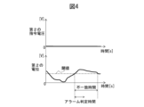
- Figure 4 is a diagram illustrating the generation of noise when the brakes of the brake device are applied.
- a potential equal to or greater than the threshold value can be determined as a high potential (H) and a potential less than the threshold value can be determined as a low potential (L).
- the threshold value is set, for example, to a value approximately halfway between the potential of the power supply 3 and the potential of the ground 4.
- the control circuit 11 applies a brake engagement open command voltage L (low) to the control terminal C1 of the first switching element SW1 as a first command voltage, and applies a brake engagement open command voltage L (low) to the control terminal C2 of the second switching element SW2 as a second command voltage. If there is no abnormality in the first switching element SW1 and the second switching element SW2, the first switching element SW1 and the second switching element SW2 open. As a result, no DC voltage is applied from the power source 3 between the first terminal P1 and the second terminal P2 of the brake coil 25, so ideally the first potential of the first terminal P1 and the second potential of the second terminal P2 should both be low potential (L).
- the first potential of the first terminal P1 and/or the second potential of the second terminal P2 becomes H (high) even though the brake device 2 is in the brake-applied state, there is a possibility that an abnormality has occurred in the first switching element SW1 and/or the second switching element SW2.
- the first potential of the first terminal P1 and/or the second potential of the second terminal P2 may become H (high) due to the influence of noise.
- the reason for this is as follows.
- the first terminal P1 and the second terminal P2 of the brake coil 25 are in a high impedance state, being disconnected from the ground 4, the first terminal P1 and the second terminal P2 of the brake coil 25 are easily affected by noise from the outside, and the magnitude of the potential fluctuates due to the noise.
- the second potential of the second terminal P2 of the brake coil 25 is shown fluctuating due to the influence of noise. If the first switching element SW1 and the second switching element SW2 are normal, when the brake of the brake device 2 is applied, the second potential should be judged to be a low potential (L), but due to the influence of noise, there may be a time when it is judged to be a high potential (H), which is "inconsistent" with the original judgment result.
- the control circuit 11 applies a pulsed test command voltage to the control terminal C1 of the first switching element SW1 and the control terminal C2 of the second switching element SW2 while applying the brake engagement command voltage when the brake device 2 is applied. That is, when the brake device 2 is applied, the control circuit 11 applies one of the brake engagement open command voltage and the pulsed test close command voltage to the control terminal C1 of the first switching element SW1 as the first command voltage, and applies one of the brake engagement open command voltage and the pulsed test close command voltage to the control terminal C2 of the second switching element SW2 as the second command voltage.
- the judgment circuit 13 judges whether or not the combination pattern of each command voltage and each detection potential matches a predetermined reference pattern when the brake engagement open command voltage and the pulsed test close command voltage are applied to the control terminals C1 and C2, respectively.
- the judgment circuit 13 judges that an abnormality has occurred in the first switching element SW1 and the second switching element SW2 when the state in which the combination pattern of each command voltage and each detection potential does not match the reference pattern (i.e., the mismatch state) continues for a predetermined mismatch judgment time.
- the judgment circuit 13 does not judge that an abnormality has occurred because there is a possibility of noise generation. Furthermore, if the combination pattern of each command voltage and each detection potential matches the reference pattern, the judgment circuit 13 naturally does not judge that an abnormality has occurred.
- the magnitude of the first potential of the first terminal P1 of the brake coil 25 and the magnitude of the second potential of the second terminal P2 of the brake coil 25 are determined according to the first command voltage applied to the control terminal C1 of the first switching element SW1 and the second command voltage applied to the control terminal C2 of the second switching element SW2.
- the combination of the first command voltage, the first potential, the second command voltage, and the second potential when the first switching element SW1 and the second switching element SW2 are normal is defined as the reference pattern.
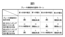
- FIG. 5 is a diagram showing a reference pattern when the brake is applied, which is used for the judgment process by the judgment circuit in the abnormality detection device according to one embodiment of the present disclosure.
- the first switching element SW1 and the second switching element SW2 are normally-off type switching elements, so the open command voltage is L (low) and the close command voltage is H (high). If the first switching element SW1 and the second switching element SW2 are normally-on type switching elements, the reference table in FIG. 5 is applied with the open command voltage being H (high) and the close command voltage being L (low).
- the control circuit 11 applies one of the brake engagement open command voltage and the pulsed test close command voltage to the control terminal C1 of the first switching element SW1 as a first command voltage, and applies one of the brake engagement open command voltage and the pulsed test close command voltage to the control terminal C2 of the second switching element SW2 as a second command voltage.
- the reference pattern when the brake is engaged includes a combination of a command voltage and a detection potential for maintaining the brake engagement state of the brake device 2, a combination of a command voltage and a detection potential when the pulsed test command voltage is applied to the control terminal C1 of the first switching element SW1, and a combination of a command voltage and a detection potential when the pulsed test command voltage is applied to the control terminal C2 of the second switching element SW2. More details are as follows.
- the reference pattern is a combination in which the first command voltage is L (low), which is the open command voltage for brake engagement, the first potential of the first terminal P1 is L (low), which is a value less than the threshold value, the second command voltage is L (low), which is the open command voltage for brake engagement, and the second potential of the second terminal P2 is L (low), which is a value less than the threshold value.
- the reference pattern is a combination in which the first command voltage is H (high), which is a test close command voltage, the first potential of the first terminal P1 is H (high), which is a value equal to or greater than a threshold value, the second command voltage is L (low), which is a brake engagement open command voltage, and the second potential of the second terminal P2 is H (high), which is a value equal to or greater than a threshold value.
- the reference pattern is a combination in which the first command voltage is L (low), which is an open command voltage for brake engagement, the first potential of the first terminal P1 is L (low), which is a value less than the threshold value, the second command voltage is H (high), which is a close command voltage for test, and the second potential of the second terminal P2 is L (low), which is a value less than the threshold value.
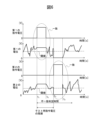
- ⁇ Waveform example> 6 is a diagram illustrating an example of a command voltage and a detected potential when each switching element is normal but there is an influence of noise when the brake of the brake device is applied in one embodiment of the present disclosure.
- Fig. 6 illustrates a case where noise occurs between the first terminal P1 and the second terminal P2 of the brake coil 25 between time t1 and time t2 and after time t4 when the brake is applied.
- the first command voltage, L (low), which is an open command voltage for brake engagement is applied to the control terminal C1 of the first switching element SW1
- the second command voltage, L (low) which is an open command voltage for brake engagement
- the second potential of the second terminal P2 is mainly L (low)
- the first potential of the first terminal P1, which should be L (low) is H (high), which is a value above the threshold, for a relatively long time due to the influence of noise. Therefore, from the start time to time t1, the combination pattern of each command voltage and each detected potential does not match the reference pattern shown in FIG. 5.
- a test close command voltage H (high) is applied as the first command voltage to the control terminal C1 of the first switching element SW1
- a brake engagement open command voltage L (low) is applied as the second command voltage to the control terminal C2 of the second switching element SW2.
- the first switching element SW1 is in the open state
- the second switching element SW2 is in the closed state.
- the first potential of the first terminal P1 becomes H (high), which is a value equal to or greater than the threshold value
- the second potential of the second terminal P2 becomes H (high), which is a value equal to or greater than the threshold value. Therefore, from time t1 to time t2, the combination pattern of each command voltage and each detected potential matches the reference pattern shown in FIG. 5, and the mismatch time from the start time to time t1 ends.
- the first command voltage, L (low), which is an open command voltage for brake engagement is applied to the control terminal C1 of the first switching element SW1
- the second command voltage, L (low) which is an open command voltage for brake engagement
- the first potential of the first terminal P1 is mainly L (low)
- the second potential of the second terminal P2, which should be L (low) is H (high), which is a value above the threshold, for a relatively long time due to the influence of noise. Therefore, from time t2 to time t3, the combination pattern of each command voltage and each detected potential does not match the reference pattern shown in FIG. 5.
- the first switching element SW1 is in an open state
- the second switching element SW2 is in a closed state.
- the first potential of the first terminal P1 becomes L (low), which is a value less than the threshold
- the second potential of the second terminal P2 becomes L (low), which is a value less than the threshold. Therefore, from time t3 to time t4, the combination pattern of each command voltage and each detected potential matches the reference pattern shown in FIG. 5, and the mismatch time from time t2 to time t3 ends.
- FIG. 7 is a diagram illustrating the command voltage and detection potential when an abnormality occurs in the first switching element SW1 when the brake of the brake device is applied in one embodiment of the present disclosure.
- FIG. 7 illustrates a case where an abnormality occurs in the first switching element SW1 at time t6 when the brake is applied. Note that, in FIG. 7, for the sake of simplicity, it is assumed that no noise is generated.
- a first command voltage, L (low), which is an open command voltage for brake engagement is applied to the control terminal C1 of the first switching element SW1
- a second command voltage, L (low) which is an open command voltage for brake engagement
- both the first switching element SW1 and the second switching element SW2 are in the open state.
- both the first potential of the first terminal P1 and the second potential of the second terminal P2 are L (low). Therefore, from the start time to time t5, the combination pattern of each command voltage and each detected potential matches the reference pattern shown in FIG. 5.
- a test close command voltage H (high) is applied as the first command voltage to the control terminal C1 of the first switching element SW1
- a brake engagement open command voltage L (low) is applied as the second command voltage to the control terminal C2 of the second switching element SW2.
- H high
- L low
- the first switching element SW1 to be in the open state
- the second switching element SW2 to be in the closed state.
- the first potential of the first terminal P1 becomes H (high), which is a value equal to or greater than the threshold
- the second potential of the second terminal P2 becomes H (high), which is a value equal to or greater than the threshold. Therefore, from time t5 to time t6, the combination pattern of each command voltage and each detected potential matches the reference pattern shown in FIG. 5.
- the first command voltage, L (low), which is an open command voltage for brake engagement is applied to the control terminal C1 of the first switching element SW1
- the second command voltage, L (low) which is an open command voltage for brake engagement
- the second switching element SW2 is in the open state, but the first switching element SW1 remains in the closed state because of a short circuit failure.
- the first potential of the first terminal P1 becomes H (high)
- the second potential of the second terminal P2 becomes H (high) for a relatively long time. Therefore, from time t6 to time t7, the combination pattern of each command voltage and each detected potential does not match the reference pattern shown in FIG. 5.
- the first switching element SW1 has a short circuit fault and remains in the closed state, and the second switching element SW2 is in the closed state.
- the first potential of the first terminal P1 becomes H (high)
- the second potential of the second terminal P2 becomes L (low). Therefore, from time t7 to time t8, the combination pattern of each command voltage and each detected potential does not match the reference pattern shown in FIG. 5.
- the first command voltage, L (low), which is an open command voltage for brake engagement is applied to the control terminal C1 of the first switching element SW1
- the second command voltage, L (low) which is an open command voltage for brake engagement
- the first switching element SW1 has a short circuit fault and remains in the closed state
- the second switching element SW2 is in the open state.
- the first potential of the first terminal P1 becomes H (high)
- the second potential of the second terminal P2 becomes H (high). Therefore, from time t7 to time t8, the combination pattern of each command voltage and each detected potential does not match the reference pattern shown in FIG. 5.
- a mismatch time counter 132 that counts the mismatch time between the combination pattern of each command voltage and each detection potential and the reference pattern, and the mismatch time counted by the mismatch time counter 132 is monitored. Once a mismatch occurs between the combination pattern of each command voltage and each detection potential and the reference pattern, the mismatch time counter 132 starts counting the mismatch time, and the count of the mismatch time counter 132 is reset when the combination pattern of each command voltage and each detection potential matches the reference pattern. If the mismatch time counted by the mismatch time counter 132 exceeds a predetermined mismatch determination time, it is determined that an abnormality has occurred in the first switching element SW1 and/or the second switching element SW2.
- a brake engagement open command voltage is mainly applied to the control terminal C1 of the first switching element SW1 and the control terminal C2 of the second switching element SW2, and a pulse-like test close command voltage is periodically applied during that time.
- the period of application of the pulsed test close command voltage is set shorter than the mismatch determination time. This means that the pattern mismatch time caused by noise is not determined to be an abnormality, and erroneous determinations caused by noise can be prevented in the abnormality detection device 1 of the non-excitation actuation type brake device 2.
- the abnormality detection device 1 can be applied not only when the brake of the brake device 2 described above is applied, but also when the brake is released.
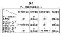
- Fig. 8 is a diagram showing a reference pattern at the time of brake release used for the determination process by the determination circuit in the abnormality detection device according to an embodiment of the present disclosure.
- the first switching element SW1 and the second switching element SW2 are normally-off type switching elements, so the open command voltage is L (low) and the close command voltage is H (high). If the first switching element SW1 and the second switching element SW2 are normally-on type switching elements, the reference table in Fig. 8 is applied by interpreting the open command voltage as H (high) and the close command voltage as L (low).
- the control circuit 11 applies one of the brake release close command voltage and the pulsed test open command voltage to the control terminal C1 of the first switching element SW1 as the first command voltage, and applies the brake release close command voltage and the pulsed test open command voltage to the control terminal C2 of the second switching element SW2 as the second command voltage.
- the reference pattern when the brake is released includes a combination of a command voltage and a detection potential for maintaining the brake mechanism state of the brake device 2, a combination of a command voltage and a detection potential when the pulsed test command voltage is applied to the control terminal C1 of the first switching element SW1, and a combination of a command voltage and a detection potential when the pulsed test command voltage is applied to the control terminal C2 of the second switching element SW2. More details are as follows.
- the reference pattern is a combination in which the first command voltage is H (high), which is a brake release close command voltage, the first potential of the first terminal P1 is H (high), which is a value equal to or greater than the threshold, the second command voltage is H (high), which is a brake release close command voltage, and the second potential of the second terminal P2 is L (low), which is a value less than the threshold.
- the reference pattern is a combination in which the first command voltage is L (low), which is a test open command voltage, the first potential of the first terminal P1 is L (low), which is a value less than the threshold value, the second command voltage is H (high), which is a brake release close command voltage, and the second potential of the second terminal P2 is L (low), which is a value less than the threshold value.
- the reference pattern is a combination in which the first command voltage is H (high), which is a brake release close command voltage, the first potential of the first terminal P1 is H (high), which is a value equal to or greater than the threshold value, the second command voltage is L (low), which is a test open command voltage, and the second potential of the second terminal P2 is H (high), which is a value equal to or greater than the threshold value.
- the first switching element SW1 and the second switching element SW2 are both in a closed state, so the path from the power source 3 through the first switching element SW1, the brake coil 25, and the second switching element SW2 to the ground 4 is in a conductive state. Therefore, the area between the first terminal P1 and the second terminal P2 of the brake coil 25 is not easily affected by external noise. Therefore, the discrepancy determination time used in the abnormality determination process by the determination circuit 13 when the brake device 2 is applied may be set shorter than the discrepancy determination time used in the abnormality determination process by the determination circuit 13 when the brake device 2 is released.
- a brake release close command voltage is mainly applied to the control terminal C1 of the first switching element SW1 and the control terminal C2 of the second switching element SW2, but a pulsed test open command voltage is periodically applied during this period.
- the period for applying the pulsed test open command voltage is set shorter than the mismatch determination time.
- the judgment circuit 13 includes a pattern judgment unit 131, a mismatch time counter 132, a mismatch time judgment unit 133, an alarm output unit 134, a test time counter 135, and a test time judgment unit 136.
- the pattern determination unit 131 determines whether the combination pattern of each command voltage and each detection potential matches a reference pattern.
- the mismatch time counter 132 stores a mismatch time count value that indicates the duration during which the combination pattern of each command voltage and each detection potential does not match the reference pattern.
- the mismatch time determination unit 133 determines whether the mismatch time count value has reached a first specified value.
- the first specified value is set to the mismatch determination time.
- the alarm output unit 134 outputs an alarm indicating that an abnormality has occurred.
- the test time counter 135 stores the test time count value.
- the test time determination unit 136 determines whether the test time count value has reached a second specified value.
- the second specified value is set to the length of one period of application of the pulsed test close command voltage.
- the test time determination unit 136 executes a determination process.
- the mismatch time counter 132 resets the mismatch time count value, and after the mismatch time counter 132 resets the mismatch time count value, the test time determination unit 136 executes a determination process.
- test time determination unit 136 determines that the test time count value has not reached the second specified value, the test time counter 135 increments the test time count value, and after the test time counter 135 increments the test time count value, the pattern determination unit 131 executes a determination process.
- test time determination unit 136 determines that the test time count value has reached the second specified value, the test time counter 135 resets the test time count value, and after the test time counter 135 resets the test time count value, the control circuit 11 applies a pulsed test command voltage to either the control terminal C1 of the first switching element SW1 or the control terminal C2 of the second switching element SW2, and after the pulsed test command voltage is applied to either the control terminal C1 of the first switching element SW1 or the control terminal C2 of the second switching element SW2, the pattern determination unit 131 executes a determination process.
- FIG. 9 is a flowchart showing the operation flow of the determination circuit in an abnormality detection device according to one embodiment of the present disclosure.
- the flowchart shown in FIG. 9 is applicable to both the brake engagement and brake release of the brake device 2, but here, the operation of the determination circuit 13 when the brake device 2 is engaged will be described.
- step S101 the test time count value of the test time counter 135 is reset.
- step S102 the control circuit 11 applies a test close command voltage to the control terminal C1 of the first switching element SW1 as the first command voltage, and applies a brake engagement open command voltage to the control terminal C2 of the second switching element SW2 as the second command voltage.
- step S103 the pattern determination unit 131 determines whether the combination pattern of each command voltage and each detection potential matches a reference pattern.
- step S103 If it is determined in step S103 that the combination pattern of each command voltage and each detection potential matches the reference pattern, the mismatch time count value of the mismatch time counter 132 is reset in step S104, and then the process proceeds to step S106.
- step S103 If it is determined in step S103 that the combination pattern of each command voltage and each detection potential does not match the reference pattern, the mismatch time count value of the mismatch time counter 132 is incremented in step S105, and then the process proceeds to step S106.
- step S106 the mismatch time determination unit 133 determines whether the mismatch time count value has reached a first specified value.
- the first specified value is set to the mismatch determination time.
- step S106 If it is determined in step S106 that the mismatch time count value has reached the first specified value, the alarm output unit 134 outputs an alarm in step S107.
- step S108 the test time determination unit 136 determines whether the test time count value has reached a second specified value.
- the second specified value is set to the length of one period of application of the pulsed test close command voltage.
- step S108 If it is not determined in step S108 that the test time count value has reached the second specified value, the test time count value of the test time counter 135 is incremented in step S109, and then the process returns to step S103.
- step S108 If it is determined in step S108 that the test time count value has reached the second specified value, proceed to step S110.
- step S110 the test time count value of the test time counter 135 is reset.
- step S111 the control circuit 11 applies a brake engagement open command voltage to the control terminal C1 of the first switching element SW1 as the first command voltage, and applies a test close command voltage to the control terminal C2 of the second switching element SW2 as the second command voltage.
- step S112 the pattern determination unit 131 determines whether the combination pattern of each command voltage and each detection potential matches a reference pattern.
- step S112 If it is determined in step S112 that the combination pattern of each command voltage and each detection potential matches the reference pattern, the mismatch time count value of the mismatch time counter 132 is reset in step S113, and then the process proceeds to step S115.
- step S112 If it is determined in step S112 that the combination pattern of each command voltage and each detection potential does not match the reference pattern, the mismatch time count value of the mismatch time counter 132 is incremented in step S114, and then the process proceeds to step S115.
- step S115 the mismatch time determination unit 133 determines whether the mismatch time count value has reached a first specified value.
- step S115 If it is determined in step S115 that the mismatch time count value has reached the first specified value, the alarm output unit 134 outputs an alarm in step S116.
- step S117 the test time determination unit 136 determines whether the test time count value has reached the second specified value.
- step S117 If it is not determined in step S117 that the test time count value has reached the second specified value, the test time count value of the test time counter 135 is incremented in step S118, and then the process returns to step S112.
- step S117 If it is determined in step S117 that the test time count value has reached the second specified value, the process returns to step S101.
- At least one processor which is an arithmetic processing device, is provided in the abnormality detection device 1.
- the arithmetic processing device include an IC, an LSI, a CPU, an MPU, and a DSP.
- the arithmetic processing device may be provided in a motor drive device to which the brake device 2 is connected.
- the arithmetic processing device has a control circuit 11, a detection circuit 12, a judgment circuit 13, and other processing units. Each of these units in the arithmetic processing device is, for example, a functional module realized by a program executed on the processor.
- control circuit 11, the detection circuit 12, the judgment circuit 13, and other processing units are constructed in a program format
- the function of each unit can be realized by operating the arithmetic processing device according to the program.
- the program for executing each process in the control circuit 11, the detection circuit 12, the judgment circuit 13, and other processing units may be provided in a form recorded on a computer-readable recording medium such as a semiconductor memory, a magnetic recording medium, or an optical recording medium.
- the control circuit 11, the detection circuit 12, the judgment circuit 13, and other processing units may be realized as a semiconductor integrated circuit in which a program for realizing the function of each unit is written.
- the memory may be provided in the motor drive device to which the brake device 2 is connected.
- the memory may be, for example, a non-volatile memory that can be electrically erased and recorded, such as an EEPROM (registered trademark), or a random access memory that can be read and written at high speed, such as a DRAM or an SRAM.
- the storage device may also have a configuration such as an HDD (hard disk drive) or an SSD (solid state drive).
- the memory stores programs for operating the control circuit 11, the detection circuit 12, the determination circuit 13, and other processing units.
- the memory also stores the mismatch time count value of the mismatch time counter 132.
- the memory also stores the test time count value of the test time counter 135.
- the memory stores a threshold value for distinguishing whether the first potential detected by the detection circuit 12 and the second battery are H (high) or L (low).
- the memory also stores various programs and various data related to the abnormality detection device 1.
- the abnormality detection device 1 According to the abnormality detection device 1 according to an embodiment of the present disclosure, it is possible to accurately detect an abnormality in the non-excitation actuation type brake device 2 both when the brake is applied and when the brake is released.
- the combination pattern of each command voltage and each detected potential does not match the reference pattern for the mismatch determination time, it is determined that an abnormality has occurred.
- the brake of the brake device 2 When the brake of the brake device 2 is applied, the first terminal P1 and the second terminal P2 of the brake coil 25 are in a high impedance state disconnected from the ground 4, so that the first terminal P1 and the second terminal P2 of the brake coil 25 are easily affected by noise from the outside.
- the combination pattern of each command voltage and each detected potential matches the reference pattern when a pulsed test command voltage is applied to the control terminal C1 of the first switching element SW1 and the control terminal C2 of the second switching element SW2, the mismatch time counter value that counts the mismatch determination time is reset. This eliminates the pattern mismatch state caused by noise, making it possible to prevent erroneous determination caused by noise.
- a control circuit 11 for controlling opening and closing of a first switching element SW1 by applying a first command voltage to a control terminal C1 of a first switching element SW1 connected between a power source 3 and a first terminal P1 of the brake coil 25, and for controlling opening and closing of a second switching element SW2 by applying a second command voltage to a control terminal C2 of a second switching element connected between a second terminal P2 of the brake coil 25 and a ground 4, of a non-excitation actuated brake device 2 that releases the brake when a current flows through a brake coil 25 and engages the brake when the current to the brake coil 25 is interrupted; a detection circuit 12 that detects a first potential that is a potential at a first terminal P1 of the brake coil 25 and a second potential that is a potential at a second terminal P2 of the brake coil 25; a determination circuit 13 that determines the presence or absence of an abnormality in the first switching element SW1 and the second switching element SW2 based on a combination pattern of the magnitude of a
- the reference pattern is a combination in which the first command voltage is a brake engagement open command voltage, the first potential is a value less than the threshold value, and the second command voltage is a brake engagement open command voltage, and the second potential is a value less than the threshold value; a combination in which the first command voltage is a test close command voltage, the first potential is a value equal to or greater than a threshold value, and the second command voltage is a brake engagement open command voltage, and the second potential is a value equal to or greater than a threshold value; a combination in which the first command voltage is a brake engagement opening command voltage, the first potential is a value less than the threshold, and the second command voltage is a test closing command voltage, and the second potential is a value less than the threshold;
- the abnormality detection device 1 according to claim 3, (Appendix 5) The abnormality detection device 1 described in Appendix 2, wherein, when the brake device 2 is released, the control circuit 11 applies, as a first command voltage, one of a brake release close command voltage and a
- the reference pattern is a combination in which the first command voltage is a brake release close command voltage, the first potential is a value equal to or greater than a threshold, and the second command voltage is a brake release close command voltage, and the second potential is a value less than the threshold; a combination in which the first command voltage is a test open command voltage, the first potential is a value less than the threshold, and the second command voltage is a brake release close command voltage, and the second potential is a value less than the threshold; a combination in which the first command voltage is a brake release close command voltage, the first potential is a value equal to or greater than a threshold, and the second command voltage is a test open command voltage, and the second potential is a value equal to or greater than a threshold;
- the abnormality detection device 1 according to claim 5, (Appendix 7) The abnormality detection device 1 described in Appendix 2, wherein the inconsistency judgment time used in the abnormality judgment processing by the judgment circuit 13 when the brake of the brake device 2 is applied is shorter than the in
- the determination circuit 13 is a pattern determination unit 131 that determines whether or not a combination pattern matches a reference pattern; a mismatch time counter 132 for storing a mismatch time count value; a mismatch time determination unit that determines whether a mismatch time count value has reached a first specified value; an alarm output unit that outputs an alarm indicating that an abnormality has occurred when it is determined by the mismatch time determination unit that the mismatch time count value has reached a first specified value; a test time counter 135 for storing a test time count value; a test time determination unit that determines whether or not a test time count value has reached a second specified value when the mismatch time determination unit determines that the mismatch time count value has not reached a first specified value; Equipped with When the pattern determination unit 131 determines that the combination pattern does not match the reference pattern, the mismatch time counter 132 increments the mismatch time count value, and after the mismatch time counter 132 increments the mismatch time count value, a determination process is performed by the test
- the mismatch time counter 132 When it is determined that the combination pattern matches the reference pattern as a result of the determination by the pattern determination unit 131, the mismatch time counter 132 resets the mismatch time count value, and after the mismatch time counter 132 resets the mismatch time count value, a determination process is performed by the test time determination unit 136.
- the test time counter 135 increments the test time count value, and after the test time counter 135 increments the test time count value, a determination process is performed by the pattern determination unit 131;
- the test time counter 135 resets the test time count value, and after the test time count value is reset by the test time counter 135, the control circuit 11 applies a pulsed test command voltage to either the control terminal C1 of the first switching element SW1 or the control terminal C2 of the second switching element SW2, and after the pulsed test command voltage is applied to either the control terminal C1 of the first switching element SW1 or the control terminal C2 of the second switching element SW2, a determination process is executed by the pattern determination unit 131.
Landscapes
- Engineering & Computer Science (AREA)
- General Engineering & Computer Science (AREA)
- Mechanical Engineering (AREA)
- Power Engineering (AREA)
- Valves And Accessory Devices For Braking Systems (AREA)
Abstract
異常検出装置は、無励磁作動型のブレーキ装置の第1のスイッチング素子の制御端子に第1の指令電圧を印加し、第2のスイッチング素子の制御端子に第2の指令電圧を印加する制御回路と、ブレーキコイルの第1の端子の電位である第1の電位と、ブレーキコイルの第2の端子の電位である第2の電位とを検出する検出回路と、制御回路が第1のスイッチング素子の制御端子に印加した第1の指令電圧と、検出回路によって検出された第1の端子の第1の電位と、制御回路が第2のスイッチング素子の制御端子に印加した第2の指令電圧と、検出回路によって検出された第2の端子の電位との組み合わせパターンに基づき、第1のスイッチング素子及び第2のスイッチング素子の異常の有無を判定する判定回路と、を備える。
Description
本開示は、ブレーキ装置の異常検出装置に関する。
モータ駆動装置では、回転しているモータにブレーキをかけたり、停止しているモータが回転しないよう固定したりするために、無励磁作動型の機械式ブレーキ装置(以下、単に「ブレーキ装置」と称する。)が広く用いられている。ブレーキ装置のブレーキコイルと電源との間にはスイッチング素子が接続されている。無励磁作動型のブレーキ装置では、スイッチング素子が閉動作することで電源からブレーキコイルに電流が流れ込み、ブレーキが解除される。また、スイッチング素子が開動作して電源からブレーキコイルに電流が流れ込まないようにすることで、ブレーキが締結される。ブレーキ装置は、安全に関わる機構であるので高い信頼性が要求される。ブレーキコイルに流れる電流を制御するスイッチング素子に異常があると、ブレーキの締結や解除が正常に行うことができない。このため、ブレーキ装置の異常を検出する技術がいくつか提案されている。
無励磁作動型のブレーキ装置の異常を正確に検出できる技術が望まれている。
本開示の一態様によれば、異常検出装置は、ブレーキコイルに電流が流れているときはブレーキを解除し、ブレーキコイルへの電流が遮断されているときはブレーキを締結する無励磁作動型のブレーキ装置の、電源とブレーキコイルの第1の端子との間に接続された第1のスイッチング素子の制御端子に第1の指令電圧を印加することで第1のスイッチング素子の開閉を制御し、ブレーキコイルの第2の端子とグランド4との間に接続された第2のスイッチング素子の制御端子に第2の指令電圧を印加することで第2のスイッチング素子の開閉を制御する制御回路と、ブレーキコイルの第1の端子の電位である第1の電位と、ブレーキコイルの第2の端子の電位である第2の電位とを検出する検出回路と、制御回路が第1のスイッチング素子の制御端子に印加した第1の指令電圧の大きさと、検出回路によって検出された第1の端子の第1の電位の大きさと、制御回路が第2のスイッチング素子の制御端子に印加した第2の指令電圧の大きさと、検出回路によって検出された第2の端子の電位の大きさとの組み合わせパターンに基づき、第1のスイッチング素子及び第2のスイッチング素子の異常の有無を判定する判定回路と、を備える。
以下、ブレーキ装置の異常検出装置を、図面を参照して説明する。なお、以下の説明では、同一または類似の機能を有する構成に同一の符号を付す。そして、それら構成の重複する説明は、省略する場合がある。理解を容易にするために、図面は縮尺を適宜変更している。また、以下の説明では、単に「ブレーキ装置」と表記するときは、無励磁作動型のブレーキ装置を意味する。
<本開示の一実施形態による全体構成>
図1は、本開示の一実施形態による異常検出装置を示す図である。
図1は、本開示の一実施形態による異常検出装置を示す図である。
本開示の一実施形態による異常検出装置1は、無励磁作動型のブレーキ装置2の異常の有無を検出する。無励磁作動型のブレーキ装置2は、ブレーキコイル25に電流が流れている励磁時にブレーキを解除し、ブレーキコイル25への電流が遮断されている無励磁時にブレーキを締結する。
本開示の一実施形態による異常検出装置1を説明するに先立ち、異常検出装置1が接続されたブレーキ駆動装置が制御するブレーキ装置2の構造について図2及び図3を参照して説明する。図2は、本開示の一実施形態による異常検出装置の異常検出対象である無励磁作動型のブレーキ装置の構造を示す断面図であって、モータに対してブレーキを締結させた状態を示す。図3は、本開示の一実施形態による異常検出装置の異常検出対象である無励磁作動型のブレーキ装置の構造を示す断面図であって、モータに対するブレーキが解除された状態を示す。
図2及び図3に示すように、ブレーキ装置2において、アマチュア22と端板23との間には摩擦板21が配置される。摩擦板21にはハブ32がスプライン結合される。ハブ32とモータのシャフト31とは例えば焼き嵌めにより一体化されているので、モータのシャフト31の回転に連動して摩擦板21も回転する。端板23とスペーサ27とはボルト28によって結合され、アマチュア22が摩擦板21に近づく方向及び遠ざかる方向に移動可能となるようにスペーサ27に結合される。コア26内にはバネ24及びブレーキコイル25が設けられる。図2に示すように、ブレーキコイル25に電流が流れていない無励磁状態においては、アマチュア22はバネ24の弾性力により摩擦板21に強く押し付けられ、摩擦板21がアマチュア22と端板23とで挟まれて回転できない。この結果、摩擦板21に結合されたモータのシャフト31も回転できなくなり、モータに対してブレーキが作動した状態となる(ブレーキ締結状態)。一方、図3に示すように、ブレーキコイル25にブレーキ電流が流れる励磁状態においては、アマチュア22を摩擦板21に押し付けていたバネ24の弾性力に打ち勝つ電磁力がコア26に発生し、これによりアマチュア22がコア26に引きつけられて摩擦板21はアマチュア22及び端板23との接触から解放される。この結果、摩擦板21ひいてはモータのシャフト31は自由に回転できるようになり、モータに対するブレーキが解除された状態となる(ブレーキ解除状態)。
図1に示すように、ブレーキ装置2には電源3が接続されている。電源3は、直流電圧を出力する。電源3は、例えば交流電圧を直流電圧に変換する整流器、スイッチングレギュレータ、あるいはバッテリなどで構成される。一例として、電源3は、電圧値が24Vの直流電圧を出力するが、その他の電圧値(例えば15V、12V、5Vなど)の直流電圧を出力する直流電源であってもよい。
ブレーキ装置2は、電源3からブレーキコイル25に流れる電流を制御するために、第1のスイッチング素子SW1と、第2のスイッチング素子SW2と、ダイオード29とを備える。
第1のスイッチング素子SW1及び第2のスイッチング素子SW2は、それぞれブレーキ装置2のブレーキコイル25に直列に接続される。ブレーキコイル25の正極端子である第1の端子P1と電源3との間の電路を開路(遮断)または閉路(接続)する第1のスイッチング素子SW1が設けられる。また、ブレーキコイル25の負極端子である第2の端子P2とグランド4との間の電路を開路(遮断)または閉路(接続)する第2のスイッチング素子SW2が設けられる。なお、図1に示す例では第1のスイッチング素子SW1及び第2のスイッチング素子SW2をそれぞれ1つずつ設けたが、この変形例として、それぞれについて2つ以上設けてもよい。第1のスイッチング素子SW1及び第2のスイッチング素子SW2の例としては、MOSFET、IGBT、サイリスタ、GTO、トランジスタなどがある。MOSFETはその端子としてゲート端子、ドレイン端子及びソース端子を有する。IGBTはその端子としてゲート端子、コレクタ端子及びエミッタ端子を有する。トランジスタはその端子としてベース端子、コレクタ端子及びエミッタ端子を有する。サイリスタ及びGTOはその端子としてゲート端子、アノード端子及びカソード端子を有する。第1のスイッチング素子SW1及び第2のスイッチング素子SW2の「電流流入端子」は、MOSFETの「ドレイン端子」、IGBT及びトランジスタの「コレクタ端子」、サイリスタ及びGTOの「アノード端子」がそれぞれ対応する。第1のスイッチング素子SW1及び第2のスイッチング素子SW2の「電流流出端子」は、MOSFETの「ソース端子」、IGBT及びトランジスタの「エミッタ端子」、サイリスタ及びGTOの「カソード端子」がそれぞれ対応する。第1のスイッチング素子SW1及び第2のスイッチング素子SW2の「制御端子」は、MOSFET、IGBT、サイリスタ及びGTOの「ゲート端子」、トランジスタの「ベース端子」がそれぞれ対応する。
第1のスイッチング素子SW1及び第2のスイッチング素子SW2の種類自体は本実施形態を限定するものではなく、例示した以外のスイッチング素子であってもよい。以下の説明では、第1のスイッチング素子SW1及び第2のスイッチング素子SW2は、一例として、ノーマリーオフ型のスイッチング素子としている。第1のスイッチング素子SW1及び第2のスイッチング素子SW2をノーマリーオン型のスイッチング素子とする場合は、以下の説明では、閉指令電圧はL(ロー)、開指令電圧はH(ハイ)と読み替えられる。
ダイオード29は、ブレーキ装置2に対して並列接続されるように、ブレーキコイル25の第1の端子P1と第2の端子P2との間に接続される。ダイオード29は、第1のスイッチング素子SW1及び第2のスイッチング素子SW2の開閉サージやノイズなどの瞬間的な高電圧を除去する。
図1に示すように、本開示の一実施形態による異常検出装置1は、制御回路11と、検出回路12と、判定回路13とを備える。
制御回路11は、第1のスイッチング素子SW1の制御端子C1に第1の指令電圧を印加することで第1のスイッチング素子SW1の開閉を制御する。また、制御回路11は、第2のスイッチング素子SW2の制御端子C2に第2の指令電圧を印加することで第2のスイッチング素子SW2の開閉を制御する。制御回路11は、ブレーキ装置2のブレーキ締結及びブレーキ解除を制御するためのブレーキ駆動装置としての機能を有するとともに、ブレーキ装置2の異常を検出するための異常検出装置1としての機能を有する。すなわち、制御回路11は、第1の指令電圧及び第2の指令電圧として、ブレーキ締結時にはブレーキ締結用指令電圧を出力し、ブレーキ解除時にはブレーキ解除用指令電圧を出力する。また、制御回路11は、第1の指令電圧及び第2の指令電圧として、パルス状のテスト用指令電圧を出力する。制御回路11から出力された第1の指令電圧は、第1のスイッチング素子SW1の制御端子C1に印加される。制御回路11から出力された第2の指令電圧は、第2のスイッチング素子SW2の制御端子C2に印加される。また、制御回路11から出力された第1の指令電圧及び第2の指令電圧に関するデータは、判定回路13に送られる。
検出回路12は、ブレーキコイル25の第1の端子P1の電位である第1の電位と、ブレーキコイル25の第2の端子P2の電位である第2の電位とを検出する。以下、検出された第1の電位及び第2の電位を、「検出電位」と称することがある。検出回路12による検出結果に関するデータは、判定回路13に送られる。
判定回路13は、制御回路11が第1のスイッチング素子SW1の制御端子C1に印加した第1の指令電圧の大きさと、第1のスイッチング素子SW1の制御端子C1に第1の指令電圧が印加されたときに検出回路12によって検出された第1の端子P1の第1の電位の大きさと、制御回路11が第2のスイッチング素子SW2の制御端子C2に印加した第2の指令電圧の大きさと、第2のスイッチング素子SW2の制御端子C2に第2の指令電圧が印加されたときに検出回路12によって検出された第2の端子P2の電位の大きさとの組み合わせパターンに基づき、第1のスイッチング素子SW1及び第2のスイッチング素子SW2の異常の有無を判定する。
判定回路13は、各指令電圧及び各検出電位の組み合わせパターンが予め規定された基準パターンとは一致しない状態が、所定の不一致判定時間にわたって継続した場合、第1のスイッチング素子SW1及び第2のスイッチング素子SW2のうちの少なくとも1つに異常が発生したと判定する。
判定回路13による判定結果を、例えば表示装置(図示せず)に表示させてもよい。表示装置の例としては、単体のディスプレイ装置、ブレーキ装置2に接続されたモータ駆動装置に付属のディスプレイ装置、上位制御装置(例えばロボットコントローラや数値制御装置)に付属のディスプレイ装置、並びに、パソコン及び携帯端末に付属のディスプレイ装置などがある。
ブレーキ装置2のブレーキ締結時においては、ノイズの影響により誤判定してしまう可能性があるので、判定回路13はノイズの影響を排除するための構成を有する。
ここで、ブレーキ締結時におけるノイズの発生について説明する。図4は、ブレーキ装置のブレーキ締結時におけるノイズの発生を例示する図である。
ブレーキコイル25の第1の端子P1の第1の電位及び第2の端子P2の第2の電位の大きさを判定するために閾値を設定することで、閾値以上の電位を高電位(H)とし、閾値未満の電位を低電位(L)として切り分けることができる。閾値は、例えば、電源3の電位とグランド4の電位とのほぼ中間の値に設定される。
ブレーキ装置2のブレーキ締結時においては、制御回路11は、第1の指令電圧として第1のスイッチング素子SW1の制御端子C1にブレーキ締結用開指令電圧であるL(ロー)を印加し、第2の指令電圧として第2のスイッチング素子SW2の制御端子C2にブレーキ締結用開指令電圧であるL(ロー)を印加する。第1のスイッチング素子SW1及び第2のスイッチング素子SW2に異常がなければ、第1のスイッチング素子SW1及び第2のスイッチング素子SW2は開動作する。これにより、ブレーキコイル25の第1の端子P1と第2の端子P2との間には電源3からの直流電圧が印加されないので、理想的には、第1の端子P1の第1の電位と第2の端子P2の第2の電位は、ともに低電位(L)になるはずである。ブレーキ装置2がブレーキ締結時にあるにもかかわらず、第1の端子P1の第1の電位及び/または第2の端子P2の第2の電位がH(ハイ)になった場合は、第1のスイッチング素子SW1及び/または第2のスイッチング素子SW2に異常が発生している可能性がある。
しかしながら、第1のスイッチング素子SW1及び第2のスイッチング素子SW2に異常が発生していなくても、ノイズの影響によって第1の端子P1の第1の電位及び/または第2の端子P2の第2の電位がH(ハイ)になることがある。その理由は次の通りである。
ブレーキコイル25の第1の端子P1と第2の端子P2との間は、グランド4から切り離されたハイインピーダンス状態となるので、ブレーキコイル25の第1の端子P1と第2の端子P2との間は、外部からのノイズの影響を受けやすくなり、ノイズに起因してその電位の大きさが変動する。図4に示す例では、ブレーキコイル25の第2の端子P2の第2の電位が、ノイズの影響を受けて変動している様子を示している。第1のスイッチング素子SW1及び第2のスイッチング素子SW2が正常であった場合は、ブレーキ装置2のブレーキ締結時においては第2の電位は、本来は低電位(L)であると判定されるべきところ、ノイズの影響により、本来の判定結果とは「不一致」となる高電位(H)と判定されてしまう時間が生じることがある。このような「不一致時間」がある程度長い時間継続し、アラーム判定時間を超えてしまうと、第1のスイッチング素子SW1及び第2のスイッチング素子SW2に異常が発生していないにもかかわらず、「異常が発生した」と誤判定してしまう。
そこで、本開示の一実施形態では、ブレーキ装置2のブレーキ締結時における上述したようなノイズに起因する誤判定を回避するために、制御回路11は、ブレーキ装置2のブレーキ締結時において、第1のスイッチング素子SW1の制御端子C1及び第2のスイッチング素子SW2の制御端子C2に対して、ブレーキ締結用指令電圧を印加している合間に、パルス状のテスト用指令電圧を印加する。すなわち、制御回路11は、ブレーキ装置2のブレーキ締結時において、第1の指令電圧として、ブレーキ締結用開指令電圧及びパルス状のテスト用閉指令電圧のうちの一方を第1のスイッチング素子SW1の制御端子C1に印加し、第2の指令電圧として、ブレーキ締結用開指令電圧及びパルス状のテスト用閉指令電圧のうちの一方を第2のスイッチング素子SW2の制御端子C2に印加する。そして、判定回路13は、各制御端子C1及びC2に対するブレーキ締結用開指令電圧及びパルス状のテスト用閉指令電圧の印加時のそれぞれにおいて、各指令電圧及び各検出電位の組み合わせパターンが予め規定された基準パターンと一致するか否かを判定する。判定回路13は、各指令電圧及び各検出電位の組み合わせパターンが基準パターンと一致しない状態(すなわち不一致である状態)が、予め規定された不一致判定時間にわたって継続した場合、第1のスイッチング素子SW1及び第2のスイッチング素子SW2に異常が発生したと判定する。また、判定回路13は、各指令電圧及び各検出電位の組み合わせパターンが基準パターンと一致しない状態(すなわち不一致である状態)が、不一致判定時間まで継続しない場合は、ノイズの発生の可能性があるので、異常とは判定しない。また、判定回路13は、各指令電圧及び各検出電位の組み合わせパターンが基準パターンと一致する場合は、当然のことながら異常とは判定しない。
<ブレーキ締結時の基準パターン>
続いて、判定回路13による判定処理に用いられるブレーキ締結時の基準パターンについて説明する。
続いて、判定回路13による判定処理に用いられるブレーキ締結時の基準パターンについて説明する。
第1のスイッチング素子SW1及び第2のスイッチング素子SW2が正常である場合、第1のスイッチング素子SW1の制御端子C1に印加される第1の指令電圧及び第2のスイッチング素子SW2の制御端子C2に印加される第2の指令電圧に応じて、ブレーキコイル25の第1の端子P1の第1の電位の大きさ及びブレーキコイル25の第2の端子P2の第2の電位の大きさが決まる。第1のスイッチング素子SW1及び第2のスイッチング素子SW2が正常である場合における第1の指令電圧と第1の電位と第2の指令電圧と第2の電位との組み合わせが、基準パターンとして規定される。
図5は、本開示の一実施形態による異常検出装置における判定回路による判定処理に用いられるブレーキ締結時の基準パターンを示す図である。なお、図5では、第1のスイッチング素子SW1及び第2のスイッチング素子SW2はノーマリーオフ型のスイッチング素子としているので、開指令電圧はL(ロー)であり、閉指令電圧はH(ハイ)である。第1のスイッチング素子SW1及び第2のスイッチング素子SW2はノーマリーオン型のスイッチング素子である場合は、図5の基準テーブルは、開指令電圧はH(ハイ)に、閉指令電圧はL(ロー)にそれぞれ読み替えて適用される。
制御回路11は、ブレーキ装置2のブレーキ締結時において、第1の指令電圧として、ブレーキ締結用開指令電圧及びパルス状のテスト用閉指令電圧のうちの一方を第1のスイッチング素子SW1の制御端子C1に印加し、第2の指令電圧として、ブレーキ締結用開指令電圧及びパルス状のテスト用閉指令電圧のうちの一方を第2のスイッチング素子SW2の制御端子C2に印加する。ブレーキ締結時における基準パターンは、ブレーキ装置2のブレーキ締結状態を維持するための指令電圧と検出電位との組み合わせと、第1のスイッチング素子SW1の制御端子C1にパルス状のテスト用指令電圧が印加されるときの指令電圧と検出電位との組み合わせと、第2のスイッチング素子SW2の制御端子C2にパルス状のテスト用指令電圧が印加されるときの指令電圧と検出電位との組み合わせとを含む。より詳細には次の通りである。
ブレーキ締結時の基本状態では、第1の指令電圧がブレーキ締結用開指令電圧であるL(ロー)であり、かつ第1の端子P1の第1の電位が閾値未満の値であるL(ロー)であり、かつ第2の指令電圧がブレーキ締結用開指令電圧であるL(ロー)であり、かつ第2の端子P2の第2の電位が閾値未満の値であるL(ロー)である組み合わせが、基準パターンとなる。
第1のスイッチング素子SW1の制御端子C1にパルス状のテスト用指令電圧が印加される状態では、第1の指令電圧がテスト用閉指令電圧であるH(ハイ)であり、かつ第1の端子P1の第1の電位が閾値以上の値であるH(ハイ)であり、かつ第2の指令電圧がブレーキ締結用開指令電圧であるL(ロー)であり、かつ第2の端子P2の第2の電位が閾値以上の値であるH(ハイ)である組み合わせが、基準パターンとなる。
第2のスイッチング素子SW2の制御端子C2にパルス状のテスト用指令電圧が印加される状態では、第1の指令電圧がブレーキ締結用開指令電圧であるL(ロー)でり、かつ第1の端子P1の第1の電位が閾値未満の値であるL(ロー)であり、かつ第2の指令電圧がテスト用閉指令電圧であるH(ハイ)であり、かつ第2の端子P2の第2の電位が閾値未満の値であるL(ロー)である組み合わせが、基準パターンとなる。
<波形例>
図6は、本開示の一実施形態において、ブレーキ装置のブレーキ締結時において各スイッチング素子が正常であるがノイズの影響がある場合の指令電圧及び検出電位を例示する図である。図6では、ブレーキ締結時において時刻t1から時刻t2までの間と時刻t4以降にブレーキコイル25の第1の端子P1と第2の端子P2との間にノイズが発生した場合を例示している。
図6は、本開示の一実施形態において、ブレーキ装置のブレーキ締結時において各スイッチング素子が正常であるがノイズの影響がある場合の指令電圧及び検出電位を例示する図である。図6では、ブレーキ締結時において時刻t1から時刻t2までの間と時刻t4以降にブレーキコイル25の第1の端子P1と第2の端子P2との間にノイズが発生した場合を例示している。
開始時刻から時刻t1までは、第1の指令電圧としてブレーキ締結用開指令電圧であるL(ロー)が第1のスイッチング素子SW1の制御端子C1に印加され、第2の指令電圧としてブレーキ締結用開指令電圧であるL(ロー)が第2のスイッチング素子SW2の制御端子C2に印加される。これにより、第1のスイッチング素子SW1及び第2のスイッチング素子SW2は、ともに開状態となる。この結果、第2の端子P2の第2の電位は主としてL(ロー)であるが、第1の端子P1の第1の電位は、本来であればL(ロー)であるべきところ、ノイズの影響により、閾値以上の値であるH(ハイ)となる時間が比較的長く発生している。よって、開始時刻から時刻t1までは、各指令電圧及び各検出電位の組み合わせパターンは、図5に示す基準パターンと不一致となる。
時刻t1から時刻t2までの間は、第1の指令電圧としてテスト用閉指令電圧であるH(ハイ)が第1のスイッチング素子SW1の制御端子C1に印加され、第2の指令電圧としてブレーキ締結用開指令電圧であるL(ロー)が第2のスイッチング素子SW2の制御端子C2に印加される。これにより、第1のスイッチング素子SW1は開状態となり、第2のスイッチング素子SW2は閉状態となる。この結果、第1の端子P1の第1の電位は閾値以上の値であるH(ハイ)となり、第2の端子P2の第2の電位は閾値以上の値であるH(ハイ)となる。よって、時刻t1から時刻t2までは、各指令電圧及び各検出電位の組み合わせパターンは、図5に示す基準パターンと一致し、開始時刻から時刻t1までの不一致時間が終了する。
時刻t2から時刻t3までの間は、第1の指令電圧としてブレーキ締結用開指令電圧であるL(ロー)が第1のスイッチング素子SW1の制御端子C1に印加され、第2の指令電圧としてブレーキ締結用開指令電圧であるL(ロー)が第2のスイッチング素子SW2の制御端子C2に印加される。これにより、第1のスイッチング素子SW1及び第2のスイッチング素子SW2は、ともに開状態となる。第1の端子P1の第1の電位は主としてL(ロー)であるが、第2の端子P2の第2の電位は、本来であればL(ロー)であるべきところ、ノイズの影響により、閾値以上の値であるH(ハイ)となる時間が比較的長く発生している。よって、時刻t2から時刻t3までは、各指令電圧及び各検出電位の組み合わせパターンは、図5に示す基準パターンと不一致となる。
時刻t3から時刻t4までの間は、第1の指令電圧としてブレーキ締結用開指令電圧であるL(ロー)が第1のスイッチング素子SW1の制御端子C1に印加され、第2の指令電圧としてテスト用閉指令電圧であるH(ハイ)が第2のスイッチング素子の制御端子C2に印加される。このとき、第1のスイッチング素子SW1は開状態となり、第2のスイッチング素子SW2は閉状態となる。この結果、第1の端子P1の第1の電位は閾値未満の値であるL(ロー)となり、第2の端子P2の第2の電位は閾値未満の値であるL(ロー)となる。よって、時刻t3から時刻t4までは、各指令電圧及び各検出電位の組み合わせパターンは、図5に示す基準パターンと一致し、時刻t2から時刻t3までの不一致時間が終了する。
図6に例示したように、各スイッチング素子が正常であるがノイズの影響を受けている場合であっても、パルス状のテスト用指令電圧が第1のスイッチング素子SW1の制御端子C1及び第2のスイッチング素子SW2の制御端子C2に印加されることによって、各指令電圧及び各検出電位の組み合わせパターンと基準パターンとが一致するので、ノイズの影響によりパターンが不一致となる時間は長くは継続しない。そこで、各指令電圧及び各検出電位の組み合わせパターンが基準パターンと一致したときは不一致判定時間を0に一旦リセットする。これにより、ノイズに起因するパターン不一致状態が異常判定処理から排除されるので、ノイズに起因する誤判定を防ぐことができる。
図7は、本開示の一実施形態において、ブレーキ装置のブレーキ締結時において第1のスイッチング素子に異常がある場合の指令電圧及び検出電位を例示する図である。図7では、ブレーキ締結時において時刻t6で第1のスイッチング素子SW1に異常が発生した場合を例示している。なお、図7では、説明を簡明なものにするために、ノイズの発生はしていないとした。
開始時刻から時刻t5までは、第1の指令電圧としてブレーキ締結用開指令電圧であるL(ロー)が第1のスイッチング素子SW1の制御端子C1に印加され、第2の指令電圧としてブレーキ締結用開指令電圧であるL(ロー)が第2のスイッチング素子SW2の制御端子C2に印加される。これにより、第1のスイッチング素子SW1及び第2のスイッチング素子SW2は、ともに開状態となる。この結果、第1の端子P1の第1の電位及び第2の端子P2の第2の電位はともにL(ロー)となる。よって、開始時刻から時刻t5までは、各指令電圧及び各検出電位の組み合わせパターンは、図5に示す基準パターンと一致する。
時刻t5から時刻t6までの間は、第1の指令電圧としてテスト用閉指令電圧であるH(ハイ)が第1のスイッチング素子SW1の制御端子C1に印加され、第2の指令電圧としてブレーキ締結用開指令電圧であるL(ロー)が第2のスイッチング素子SW2の制御端子C2に印加される。これにより、第1のスイッチング素子SW1は開状態となり、第2のスイッチング素子SW2は閉状態となる。この結果、第1の端子P1の第1の電位は閾値以上の値であるH(ハイ)となり、第2の端子P2の第2の電位は閾値以上の値であるH(ハイ)となる。よって、時刻t5から時刻t6までは、各指令電圧及び各検出電位の組み合わせパターンは、図5に示す基準パターンと一致する。
時刻t6以降、第1のスイッチング素子SW1に異常(ショート故障)が発生している。
時刻t6から時刻t7までの間は、第1の指令電圧としてブレーキ締結用開指令電圧であるL(ロー)が第1のスイッチング素子SW1の制御端子C1に印加され、第2の指令電圧としてブレーキ締結用開指令電圧であるL(ロー)が第2のスイッチング素子SW2の制御端子C2に印加される。このとき、第2のスイッチング素子SW2は開状態となるが、第1のスイッチング素子SW1はショート故障しているので閉状態のままである。この結果、第1の端子P1の第1の電位はH(ハイ)となり、第2の端子P2の第2の電位はH(ハイ)となる時間が比較的長く発生する。よって、時刻t6から時刻t7までは、各指令電圧及び各検出電位の組み合わせパターンは、図5に示す基準パターンと不一致となる。
時刻t7から時刻t8までの間は、第1の指令電圧としてブレーキ締結用開指令電圧であるL(ロー)が第1のスイッチング素子SW1の制御端子C1に印加され、第2の指令電圧としてテスト用閉指令電圧であるH(ハイ)が第2のスイッチング素子SW2の制御端子C2に印加される。このとき、第1のスイッチング素子SW1はショート故障しているので閉状態のままであり、第2のスイッチング素子SW2は閉状態となる。この結果、第1の端子P1の第1の電位はH(ハイ)となり、第2の端子P2の第2の電位はL(ロー)となる。よって、時刻t7から時刻t8までは、各指令電圧及び各検出電位の組み合わせパターンは、図5に示す基準パターンと不一致となる。
時刻t8から時刻t9までは、第1の指令電圧としてブレーキ締結用開指令電圧であるL(ロー)が第1のスイッチング素子SW1の制御端子C1に印加され、第2の指令電圧としてブレーキ締結用開指令電圧であるL(ロー)が第2のスイッチング素子SW2の制御端子C2に印加される。このとき、第1のスイッチング素子SW1はショート故障しているので閉状態のままであり、第2のスイッチング素子SW2は、開状態となる。この結果、第1の端子P1の第1の電位はH(ハイ)となり、第2の端子P2の第2の電位はH(ハイ)となる。よって、時刻t7から時刻t8までは、各指令電圧及び各検出電位の組み合わせパターンは、図5に示す基準パターンと不一致となる。
図7に例示したように、第1のスイッチング素子SW1に異常が発生した時刻t6以降において、各指令電圧及び各検出電位の組み合わせパターンと基準パターンとの不一致が一旦発生すると、それ以降はパターン不一致時間が継続することになる。第2のスイッチング素子SW2に異常が発生しても同様である。
上述した図6及び図7から、各指令電圧及び各検出電位の組み合わせパターンが基準パターンと一致したときに不一致判定時間を0に一旦リセットすれば、「各指令電圧及び各検出電位の組み合わせパターンが基準パターンとは一致しない状態が不一致判定時間にわたって継続した場合に1のスイッチング素子SW1及び第2のスイッチング素子SW2に異常が発生した」という判定処理を行ったとしても、ノイズに起因する誤判定は発生しないことが分かる。
そこで、本開示の実施形態では、各指令電圧及び各検出電位の組み合わせパターンと基準パターンとの不一致時間をカウントする不一致時間カウンタ132を設け、不一致時間カウンタ132によりカウントされた不一致時間を監視する。各指令電圧及び各検出電位の組み合わせパターンと基準パターンとの不一致が一旦発生したら、不一致時間カウンタ132による不一致時間のカウントを開始し、各指令電圧及び各検出電位の組み合わせパターンと基準パターンとが一致した時点で不一致時間カウンタ132のカウントをリセットする。不一致時間カウンタ132によるカウントされた不一致時間が、所定の不一致判定時間を超えた場合は、第1のスイッチング素子SW1及び/または第2のスイッチング素子SW2に異常が発生したと判定する。ブレーキ装置2のブレーキ締結時には、第1のスイッチング素子SW1の制御端子C1及び第2のスイッチング素子SW2の制御端子C2には、主としてブレーキ締結用開指令電圧が印加されるが、その間にもパルス状のテスト用閉指令電圧が周期的に印加される。パルス状のテスト用閉指令電圧の印加の周期は、不一致判定時間よりも短く設定される。これにより、ノイズに起因するパターン不一致時間は異常と判定されなくなり、無励磁作動型のブレーキ装置2の異常検出装置1においてノイズに起因する誤判定を防ぐことができる。
本開示の一実施形態による異常検出装置1は、上述したブレーキ装置2のブレーキ締結時に加え、ブレーキ解除時にも同様に適用することができる。
<ブレーキ解除時の基準パターン>
図8は、本開示の一実施形態による異常検出装置における判定回路による判定処理に用いられるブレーキ解除時の基準パターンを示す図である。なお、図8では、第1のスイッチング素子SW1及び第2のスイッチング素子SW2はノーマリーオフ型のスイッチング素子としているので、開指令電圧はL(ロー)であり、閉指令電圧はH(ハイ)である。第1のスイッチング素子SW1及び第2のスイッチング素子SW2はノーマリーオン型のスイッチング素子である場合は、図8の基準テーブルは、開指令電圧はH(ハイ)に、閉指令電圧はL(ロー)にそれぞれ読み替えて適用される。
図8は、本開示の一実施形態による異常検出装置における判定回路による判定処理に用いられるブレーキ解除時の基準パターンを示す図である。なお、図8では、第1のスイッチング素子SW1及び第2のスイッチング素子SW2はノーマリーオフ型のスイッチング素子としているので、開指令電圧はL(ロー)であり、閉指令電圧はH(ハイ)である。第1のスイッチング素子SW1及び第2のスイッチング素子SW2はノーマリーオン型のスイッチング素子である場合は、図8の基準テーブルは、開指令電圧はH(ハイ)に、閉指令電圧はL(ロー)にそれぞれ読み替えて適用される。
制御回路11は、ブレーキ装置2のブレーキ解除時において、第1の指令電圧として、ブレーキ解除用閉指令電圧及びパルス状のテスト用開指令電圧のうちの一方を第1のスイッチング素子SW1の制御端子C1に印加し、第2の指令電圧として、ブレーキ解除用閉指令電圧及びパルス状のテスト用開指令電圧を第2のスイッチング素子SW2の制御端子C2に印加する。ブレーキ解除時における基準パターンは、ブレーキ装置2のブレーキ機序状態を維持するための指令電圧と検出電位との組み合わせと、第1のスイッチング素子SW1の制御端子C1にパルス状のテスト用指令電圧が印加されるときの指令電圧と検出電位との組み合わせと、第2のスイッチング素子SW2の制御端子C2にパルス状のテスト用指令電圧が印加されるときの指令電圧と検出電位との組み合わせとを含む。より詳細には次の通りである。
ブレーキ解除時の基本状態では、第1の指令電圧がブレーキ解除用閉指令電圧であるH(ハイ)であり、かつ第1の端子P1の第1の電位が閾値以上の値であるH(ハイ)であり、かつ第2の指令電圧がブレーキ解除用閉指令電圧であるH(ハイ)であり、かつ第2の端子P2の第2の電位が閾値未満の値であるL(ロー)である組み合わせが、基準パターンとなる。
第1のスイッチング素子SW1の制御端子C1にパルス状のテスト用指令電圧が印加される状態では、第1の指令電圧がテスト用開指令電圧であるL(ロー)であり、かつ第1の端子P1の第1の電位が閾値未満の値であるL(ロー)であり、かつ第2の指令電圧がブレーキ解除用閉指令電圧であるH(ハイ)であり、かつ第2の端子P2の第2の電位が閾値未満の値であるL(ロー)である組み合わせが、基準パターンとなる。
第2のスイッチング素子SW2の制御端子C2にパルス状のテスト用指令電圧が印加される状態では、第1の指令電圧がブレーキ解除用閉指令電圧であるH(ハイ)であり、かつ第1の端子P1の第1の電位が閾値以上の値であるH(ハイ)であり、かつ第2の指令電圧がテスト用開指令電圧であるL(ロー)であり、かつ第2の端子P2の第2の電位が閾値以上の値であるH(ハイ)である組み合わせが、基準パターンとなる。
なお、ブレーキ装置2のブレーキ解除時は、第1のスイッチング素子SW1及び第2のスイッチング素子SW2はともに閉状態にあるので、電源3から第1のスイッチング素子SW1、ブレーキコイル25、第2のスイッチング素子SW2を経てグランド4に至るまでの経路は導通状態にある。よって、ブレーキコイル25の第1の端子P1と第2の端子P2との間は、外部からのノイズの影響を受けにくい。したがって、ブレーキ装置2のブレーキ締結時において判定回路13による異常判定処理に用いられる不一致判定時間は、ブレーキ装置2のブレーキ解除時において判定回路13による異常判定処理に用いられる不一致判定時間よりも短く設定されてもよい。
ブレーキ装置2のブレーキ解除時には、第1のスイッチング素子SW1の制御端子C1及び第2のスイッチング素子SW2の制御端子C2には、主としてブレーキ解除用閉指令電圧が印加されるが、その間にもパルス状のテスト用開指令電圧が周期的に印加される。パルス状のテスト用開指令電圧の印加の周期は、不一致判定時間よりも短く設定される。これにより、仮にノイズが発生したとしても当該ノイズに起因するパターン不一致時間は異常と判定されなくなり、無励磁作動型のブレーキ装置2の異常検出装置1においてノイズに起因する誤判定をより確実に防ぐことができる。
<判定回路の詳細>
上述した判定回路13による判定処理を実現するために、判定回路13は、パターン判定部131と、不一致時間カウンタ132と、不一致時間判定部133と、アラーム出力部134と、テスト時間カウンタ135と、テスト時間判定部136とを備える。
上述した判定回路13による判定処理を実現するために、判定回路13は、パターン判定部131と、不一致時間カウンタ132と、不一致時間判定部133と、アラーム出力部134と、テスト時間カウンタ135と、テスト時間判定部136とを備える。
パターン判定部131は、各指令電圧及び各検出電位の組み合わせパターンが基準パターンと一致するか否かを判定する。
不一致時間カウンタ132は、各指令電圧及び各検出電位の組み合わせパターンと基準パターンとが不一致となる継続時間を示す不一致時間カウント値を格納する。
不一致時間判定部133は、不一致時間カウント値が第1の規定値に達したか否かを判定する。第1の規定値は、不一致判定時間に設定される。
アラーム出力部134は、不一致時間判定部133による判定の結果、不一致時間カウント値が第1の規定値に達したと判定された場合、異常が発生したことを示すアラームを出力する。
テスト時間カウンタ135は、テスト時間カウント値を格納する。
テスト時間判定部136は、不一致時間判定部133による判定の結果、不一致時間カウント値が第1の規定値に達したと判定されなかった場合、テスト時間カウント値が第2の規定値に達したか否かを判定する。第2の規定値は、パルス状のテスト用閉指令電圧の印加の1周期の長さに設定される。
パターン判定部131による判定の結果、各指令電圧及び各検出電位の組み合わせパターンが基準パターンと一致すると判定されなかった場合は、不一致時間カウンタ132は不一致時間カウント値をインクリメントし、かつ、不一致時間カウンタ132により不一致時間カウント値がインクリメントされた後に、テスト時間判定部136による判定処理が実行される。
パターン判定部131による判定の結果、各指令電圧及び各検出電位の組み合わせパターンが基準パターンと一致すると判定された場合は、不一致時間カウンタ132は不一致時間カウント値をリセットし、かつ、不一致時間カウンタ132により不一致時間カウント値がリセットされた後に、テスト時間判定部136による判定処理が実行される。
テスト時間判定部136による判定の結果、テスト時間カウント値が第2の規定値に達したと判定されなかった場合は、テスト時間カウンタ135はテスト時間カウント値をインクリメントし、かつ、テスト時間カウンタ135によりテスト時間カウント値がインクリメントされた後に、パターン判定部131による判定処理が実行される。
テスト時間判定部136による判定の結果、テスト時間カウント値が第2の規定値に達したと判定された場合は、テスト時間カウンタ135はテスト時間カウント値をリセットし、かつ、テスト時間カウンタ135によりテスト時間カウント値がリセットされた後に、制御回路11はパルス状のテスト用指令電圧を第1のスイッチング素子SW1の制御端子C1及び第2のスイッチング素子SW2の制御端子C2のうちのいずれかに印加し、かつ、パルス状のテスト用指令電圧が第1のスイッチング素子SW1の制御端子C1及び第2のスイッチング素子SW2の制御端子C2のうちのいずれかに印加された後に、パターン判定部131による判定処理が実行される。
図9は、本開示の一実施形態による異常検出装置における判定回路の動作フローを示すフローチャートである。図9に示すフローチャートはブレーキ装置2のブレーキ締結及びブレーキ解除のいずれの場合においても適用可能であるが、ここでは、ブレーキ装置2のブレーキ締結時の判定回路13の動作について説明する。
ブレーキ装置2のブレーキ締結時において、ステップS101において、テスト時間カウンタ135のテスト時間カウント値がリセットされる。
ステップS102において、制御回路11は、第1の指令電圧として第1のスイッチング素子SW1の制御端子C1にテスト用閉指令電圧を印加し、第2の指令電圧として第2のスイッチング素子SW2の制御端子C2にブレーキ締結用開指令電圧を印加する。
ステップS103において、パターン判定部131は、各指令電圧及び各検出電位の組み合わせパターンが基準パターンと一致するか否かを判定する。
ステップS103において各指令電圧及び各検出電位の組み合わせパターンが基準パターンと一致すると判定された場合は、ステップS104において、不一致時間カウンタ132の不一致時間カウント値がリセットされ、その後、ステップS106へ進む。
ステップS103において各指令電圧及び各検出電位の組み合わせパターンが基準パターンと一致しないと判定された場合は、ステップS105において、不一致時間カウンタ132の不一致時間カウント値がインクリメントされ、その後、ステップS106へ進む。
ステップS106において、不一致時間判定部133は、不一致時間カウント値が第1の規定値に達したか否かを判定する。第1の規定値は、不一致判定時間に設定されている。
ステップS106において不一致時間カウント値が第1の規定値に達したと判定された場合は、ステップS107において、アラーム出力部134は、アラームを出力する。
ステップS107において不一致時間カウント値が第1の規定値に達したと判定されなかった場合は、ステップS108において、テスト時間判定部136は、テスト時間カウント値が第2の規定値に達したか否かを判定する。第2の規定値は、パルス状のテスト用閉指令電圧の印加の1周期の長さに設定されている。
ステップS108においてテスト時間カウント値が第2の規定値に達したと判定されなかった場合は、ステップS109において、テスト時間カウンタ135のテスト時間カウント値がインクリメントされ、その後、ステップS103へ戻る。
ステップS108においてテスト時間カウント値が第2の規定値に達したと判定された場合は、ステップS110へ進む。
ステップS110において、テスト時間カウンタ135のテスト時間カウント値がリセットされる。
ステップS111において、制御回路11は、第1の指令電圧として第1のスイッチング素子SW1の制御端子C1にブレーキ締結用開指令電圧を印加し、第2の指令電圧として第2のスイッチング素子SW2の制御端子C2にテスト用閉指令電圧を印加する。
ステップS112において、パターン判定部131は、各指令電圧及び各検出電位の組み合わせパターンが基準パターンと一致するか否かを判定する。
ステップS112において各指令電圧及び各検出電位の組み合わせパターンが基準パターンと一致すると判定された場合は、ステップS113において、不一致時間カウンタ132の不一致時間カウント値がリセットされ、その後、ステップS115へ進む。
ステップS112において各指令電圧及び各検出電位の組み合わせパターンが基準パターンと一致しないと判定された場合は、ステップS114において、不一致時間カウンタ132の不一致時間カウント値がインクリメントされ、その後、ステップS115へ進む。
ステップS115において、不一致時間判定部133は、不一致時間カウント値が第1の規定値に達したか否かを判定する。
ステップS115において不一致時間カウント値が第1の規定値に達したと判定された場合は、ステップS116において、アラーム出力部134は、アラームを出力する。
ステップS115において不一致時間カウント値が第1の規定値に達したと判定されなかった場合は、ステップS117において、テスト時間判定部136は、テスト時間カウント値が第2の規定値に達したか否かを判定する。
ステップS117においてテスト時間カウント値が第2の規定値に達したと判定されなかった場合は、ステップS118において、テスト時間カウンタ135のテスト時間カウント値がインクリメントされ、その後、ステップS112へ戻る。
ステップS117においてテスト時間カウント値が第2の規定値に達したと判定された場合は、ステップS101へ戻る。
<プロセッサ及びメモリ>
異常検出装置1内には、演算処理装置である少なくとも1つのプロセッサが設けられる。演算処理装置としては、例えばIC、LSI、CPU、MPU、DSPなどがある。演算処理装置は、ブレーキ装置2が接続されるモータ駆動装置内に設けられてもよい。演算処理装置は、制御回路11、検出回路12、判定回路13、及びその他の処理部を有する。演算処理装置が有するこれらの各部は、例えば、プロセッサ上で実行されるプログラムにより実現される機能モジュールである。例えば、制御回路11、検出回路12、判定回路13、及びその他の処理部をプログラム形式で構築する場合は、演算処理装置をこのプログラムに従って動作させることで、各部の機能を実現することができる。制御回路11、検出回路12、判定回路13、及びその他の処理部における各処理を実行するためのプログラムは、半導体メモリ、磁気記録媒体または光記録媒体といった、コンピュータ読取可能な記録媒体に記録された形で提供されてもよい。またあるいは、制御回路11、検出回路12、判定回路13、及びその他の処理部を、各部の機能を実現するプログラムを書き込んだ半導体集積回路として実現してもよい。
異常検出装置1内には、演算処理装置である少なくとも1つのプロセッサが設けられる。演算処理装置としては、例えばIC、LSI、CPU、MPU、DSPなどがある。演算処理装置は、ブレーキ装置2が接続されるモータ駆動装置内に設けられてもよい。演算処理装置は、制御回路11、検出回路12、判定回路13、及びその他の処理部を有する。演算処理装置が有するこれらの各部は、例えば、プロセッサ上で実行されるプログラムにより実現される機能モジュールである。例えば、制御回路11、検出回路12、判定回路13、及びその他の処理部をプログラム形式で構築する場合は、演算処理装置をこのプログラムに従って動作させることで、各部の機能を実現することができる。制御回路11、検出回路12、判定回路13、及びその他の処理部における各処理を実行するためのプログラムは、半導体メモリ、磁気記録媒体または光記録媒体といった、コンピュータ読取可能な記録媒体に記録された形で提供されてもよい。またあるいは、制御回路11、検出回路12、判定回路13、及びその他の処理部を、各部の機能を実現するプログラムを書き込んだ半導体集積回路として実現してもよい。
また、異常検出装置1内には、記憶装置である少なくとも1つのメモリが設けられる。メモリは、ブレーキ装置2が接続されるモータ駆動装置内に設けられてもよい。メモリとしては、例えばEEPROM(登録商標)などのような電気的に消去・記録可能な不揮発性メモリ、または、例えばDRAM、SRAMなどのような高速で読み書きのできるランダムアクセスメモリなどがある。また、記憶装置は、例えばHDD(ハードディスクドライブ)やSSD(ソリッドステートドライブ)などのような構成を有してもよい。メモリには、制御回路11、検出回路12、判定回路13、及びその他の処理部を動作させるためのプログラムが格納される。また、メモリには、不一致時間カウンタ132の不一致時間カウント値が格納される。また、メモリには、テスト時間カウンタ135のテスト時間カウント値が格納される。メモリには、検出回路12が検出した第1の電位及び第2の電池がH(ハイ)であるかL(ロー)であるかを切り分けるための閾値が格納される。また、メモリには、異常検出装置1に関連する各種プログラム及び各種データが格納される。
<異常検出装置の動作>
本開示の一実施形態による異常検出装置1によれば、無励磁作動型のブレーキ装置2のブレーキ締結時及びブレーキ解除時のいずれにおいてもブレーキ装置2の異常を正確に検出することができる。
本開示の一実施形態による異常検出装置1によれば、無励磁作動型のブレーキ装置2のブレーキ締結時及びブレーキ解除時のいずれにおいてもブレーキ装置2の異常を正確に検出することができる。
上述したように、本開示の一実施形態では、各指令電圧及び各検出電位の組み合わせパターンが基準パターンと一致しない状態が、不一致判定時間にわたって継続した場合は、異常が発生と判定する。ブレーキ装置2のブレーキ締結時はブレーキコイル25の第1の端子P1と第2の端子P2との間は、グランド4から切り離されたハイインピーダンス状態となるので、ブレーキコイル25の第1の端子P1と第2の端子P2との間は、外部からのノイズの影響を受けやすくなる。第1のスイッチング素子SW1の制御端子C1及び第2のスイッチング素子SW2の制御端子C2にパルス状のテスト用指令電圧が印加されたときに各指令電圧及び各検出電位の組み合わせパターンが基準パターンと一致した場合は、不一致判定時間をカウントする不一致時間カウンタ値がリセットされる。これにより、ノイズに起因するパターン不一致状態が排除されるので、ノイズに起因する誤判定を防ぐことができる。
以上、本開示について詳述したが、本開示は上述した個々の実施形態に限定されるものではない。これらの実施形態は、本開示の要旨を逸脱しない範囲で、または、特許請求の範囲に記載された内容とその均等物から導き出される本開示の趣旨を逸脱しない範囲で、種々の追加、置き換え、変更、部分的削除等が可能である。また、これらの実施形態は、組み合わせて実施することもできる。例えば、上述した実施形態において、各動作の順序や各処理の順序は、一例として示したものであり、これらに限定されるものではない。また、上述した実施形態の説明に数値又は数式が用いられている場合も同様である。
<付記>
上記実施形態に関し、更に以下の付記を開示する。
上記実施形態に関し、更に以下の付記を開示する。
(付記1)
ブレーキコイル25に電流が流れているときはブレーキを解除し、ブレーキコイル25への電流が遮断されているときはブレーキを締結する無励磁作動型のブレーキ装置2の、電源3とブレーキコイル25の第1の端子P1との間に接続された第1のスイッチング素子SW1の制御端子C1に第1の指令電圧を印加することで第1のスイッチング素子SW1の開閉を制御し、ブレーキコイル25の第2の端子P2とグランド4との間に接続された第2のスイッチング素子の制御端子C2に第2の指令電圧を印加することで第2のスイッチング素子SW2の開閉を制御する制御回路11と、
ブレーキコイル25の第1の端子P1の電位である第1の電位と、ブレーキコイル25の第2の端子P2の電位である第2の電位とを検出する検出回路12と、
制御回路11が第1のスイッチング素子SW1の制御端子C1に印加した第1の指令電圧の大きさと、検出回路12によって検出された第1の端子P1の第1の電位の大きさと、制御回路11が第2のスイッチング素子SW2の制御端子C2に印加した第2の指令電圧の大きさと、検出回路12によって検出された第2の端子P2の電位の大きさとの組み合わせパターンに基づき、第1のスイッチング素子SW1及び第2のスイッチング素子SW2の異常の有無を判定する判定回路13と、
を備える異常検出装置1。
(付記2)
判定回路13は、組み合わせパターンが予め規定された基準パターンとは一致しない状態が、所定の不一致判定時間にわたって継続した場合、第1のスイッチング素子SW1及び第2のスイッチング素子SW2に異常が発生したと判定する、付記1に記載の異常検出装置1。
(付記3)
制御回路11は、ブレーキ装置2のブレーキ締結時において、第1の指令電圧として、ブレーキ締結用開指令電圧及びパルス状のテスト用閉指令電圧のうちの一方を第1のスイッチング素子SW1の制御端子C1に印加し、第2の指令電圧として、ブレーキ締結用開指令電圧及びパルス状のテスト用閉指令電圧のうちの一方を第2のスイッチング素子SW2の制御端子C2に印加する、付記2に記載の異常検出装置1。
(付記4)
基準パターンは、
第1の指令電圧がブレーキ締結用開指令電圧であり、かつ第1の電位が閾値未満の値であり、かつ第2の指令電圧がブレーキ締結用開指令電圧であり、かつ第2の電位が閾値未満の値である組み合わせと、
第1の指令電圧がテスト用閉指令電圧であり、かつ第1の電位が閾値以上の値であり、かつ第2の指令電圧がブレーキ締結用開指令電圧であり、かつ第2の電位が閾値以上の値である組み合わせと、
第1の指令電圧がブレーキ締結用開指令電圧であり、かつ第1の電位が閾値未満の値であり、かつ第2の指令電圧がテスト用閉指令電圧であり、かつ第2の電位が閾値未満の値である組み合わせと、
を含む、付記3に記載の異常検出装置1。
(付記5)
制御回路11は、ブレーキ装置2のブレーキ解除時において、第1の指令電圧として、ブレーキ解除用閉指令電圧及びパルス状のテスト用開指令電圧のうちの一方を第1のスイッチング素子SW1の制御端子C1に印加し、第2の指令電圧として、ブレーキ解除用閉指令電圧及びパルス状のテスト用開指令電圧を第2のスイッチング素子SW2の制御端子C2に印加する、付記2に記載の異常検出装置1。
(付記6)
基準パターンは、
第1の指令電圧がブレーキ解除用閉指令電圧であり、かつ第1の電位が閾値以上の値であり、かつ第2の指令電圧がブレーキ解除用閉指令電圧であり、かつ第2の電位が閾値未満の値である組み合わせと、
第1の指令電圧がテスト用開指令電圧であり、かつ第1の電位が閾値未満の値であり、かつ第2の指令電圧がブレーキ解除用閉指令電圧であり、かつ第2の電位が閾値未満の値である組み合わせと、
第1の指令電圧がブレーキ解除用閉指令電圧であり、かつ第1の電位が閾値以上の値であり、かつ第2の指令電圧がテスト用開指令電圧であり、かつ第2の電位が閾値以上の値である組み合わせと、
を含む、付記5に記載の異常検出装置1。
(付記7)
ブレーキ装置2のブレーキ締結時において判定回路13による異常判定処理に用いられる不一致判定時間は、ブレーキ装置2のブレーキ解除時において判定回路13による異常判定処理に用いられる不一致判定時間よりも短い、付記2に記載の異常検出装置1。
(付記8)
判定回路13は、
組み合わせパターンが基準パターンと一致するか否かを判定するパターン判定部131と、
不一致時間カウント値を格納する不一致時間カウンタ132と、
不一致時間カウント値が第1の規定値に達したか否かを判定する不一致時間判定部133と、
不一致時間判定部133による判定の結果、不一致時間カウント値が第1の規定値に達したと判定された場合、異常が発生したことを示すアラームを出力するアラーム出力部134と、
テスト時間カウント値を格納するテスト時間カウンタ135と、
不一致時間判定部133による判定の結果、不一致時間カウント値が第1の規定値に達したと判定されなかった場合、テスト時間カウント値が第2の規定値に達したか否かを判定するテスト時間判定部136と、
を備え、
パターン判定部131による判定の結果、組み合わせパターンが基準パターンと一致すると判定されなかった場合は、不一致時間カウンタ132は不一致時間カウント値をインクリメントし、かつ、不一致時間カウンタ132により不一致時間カウント値がインクリメントされた後に、テスト時間判定部136による判定処理が実行され、
パターン判定部131による判定の結果、組み合わせパターンが基準パターンと一致すると判定された場合は、不一致時間カウンタ132は不一致時間カウント値をリセットし、かつ、不一致時間カウンタ132により不一致時間カウント値がリセットされた後に、テスト時間判定部136による判定処理が実行され、
テスト時間判定部136による判定の結果、テスト時間カウント値が第2の規定値に達したと判定されなかった場合は、テスト時間カウンタ135はテスト時間カウント値をインクリメントし、かつ、テスト時間カウンタ135によりテスト時間カウント値がインクリメントされた後に、パターン判定部131による判定処理が実行され、
テスト時間判定部136による判定の結果、テスト時間カウント値が第2の規定値に達したと判定された場合は、テスト時間カウンタ135はテスト時間カウント値をリセットし、かつ、テスト時間カウンタ135によりテスト時間カウント値がリセットされた後に、制御回路11はパルス状のテスト用指令電圧を第1のスイッチング素子SW1の制御端子C1及び第2のスイッチング素子SW2の制御端子C2のうちのいずれかに印加し、かつ、パルス状のテスト用指令電圧が第1のスイッチング素子SW1の制御端子C1及び第2のスイッチング素子SW2の制御端子C2のうちのいずれかに印加された後に、パターン判定部131による判定処理が実行される、付記2~7のいずれか1つに記載の異常検出装置1。
ブレーキコイル25に電流が流れているときはブレーキを解除し、ブレーキコイル25への電流が遮断されているときはブレーキを締結する無励磁作動型のブレーキ装置2の、電源3とブレーキコイル25の第1の端子P1との間に接続された第1のスイッチング素子SW1の制御端子C1に第1の指令電圧を印加することで第1のスイッチング素子SW1の開閉を制御し、ブレーキコイル25の第2の端子P2とグランド4との間に接続された第2のスイッチング素子の制御端子C2に第2の指令電圧を印加することで第2のスイッチング素子SW2の開閉を制御する制御回路11と、
ブレーキコイル25の第1の端子P1の電位である第1の電位と、ブレーキコイル25の第2の端子P2の電位である第2の電位とを検出する検出回路12と、
制御回路11が第1のスイッチング素子SW1の制御端子C1に印加した第1の指令電圧の大きさと、検出回路12によって検出された第1の端子P1の第1の電位の大きさと、制御回路11が第2のスイッチング素子SW2の制御端子C2に印加した第2の指令電圧の大きさと、検出回路12によって検出された第2の端子P2の電位の大きさとの組み合わせパターンに基づき、第1のスイッチング素子SW1及び第2のスイッチング素子SW2の異常の有無を判定する判定回路13と、
を備える異常検出装置1。
(付記2)
判定回路13は、組み合わせパターンが予め規定された基準パターンとは一致しない状態が、所定の不一致判定時間にわたって継続した場合、第1のスイッチング素子SW1及び第2のスイッチング素子SW2に異常が発生したと判定する、付記1に記載の異常検出装置1。
(付記3)
制御回路11は、ブレーキ装置2のブレーキ締結時において、第1の指令電圧として、ブレーキ締結用開指令電圧及びパルス状のテスト用閉指令電圧のうちの一方を第1のスイッチング素子SW1の制御端子C1に印加し、第2の指令電圧として、ブレーキ締結用開指令電圧及びパルス状のテスト用閉指令電圧のうちの一方を第2のスイッチング素子SW2の制御端子C2に印加する、付記2に記載の異常検出装置1。
(付記4)
基準パターンは、
第1の指令電圧がブレーキ締結用開指令電圧であり、かつ第1の電位が閾値未満の値であり、かつ第2の指令電圧がブレーキ締結用開指令電圧であり、かつ第2の電位が閾値未満の値である組み合わせと、
第1の指令電圧がテスト用閉指令電圧であり、かつ第1の電位が閾値以上の値であり、かつ第2の指令電圧がブレーキ締結用開指令電圧であり、かつ第2の電位が閾値以上の値である組み合わせと、
第1の指令電圧がブレーキ締結用開指令電圧であり、かつ第1の電位が閾値未満の値であり、かつ第2の指令電圧がテスト用閉指令電圧であり、かつ第2の電位が閾値未満の値である組み合わせと、
を含む、付記3に記載の異常検出装置1。
(付記5)
制御回路11は、ブレーキ装置2のブレーキ解除時において、第1の指令電圧として、ブレーキ解除用閉指令電圧及びパルス状のテスト用開指令電圧のうちの一方を第1のスイッチング素子SW1の制御端子C1に印加し、第2の指令電圧として、ブレーキ解除用閉指令電圧及びパルス状のテスト用開指令電圧を第2のスイッチング素子SW2の制御端子C2に印加する、付記2に記載の異常検出装置1。
(付記6)
基準パターンは、
第1の指令電圧がブレーキ解除用閉指令電圧であり、かつ第1の電位が閾値以上の値であり、かつ第2の指令電圧がブレーキ解除用閉指令電圧であり、かつ第2の電位が閾値未満の値である組み合わせと、
第1の指令電圧がテスト用開指令電圧であり、かつ第1の電位が閾値未満の値であり、かつ第2の指令電圧がブレーキ解除用閉指令電圧であり、かつ第2の電位が閾値未満の値である組み合わせと、
第1の指令電圧がブレーキ解除用閉指令電圧であり、かつ第1の電位が閾値以上の値であり、かつ第2の指令電圧がテスト用開指令電圧であり、かつ第2の電位が閾値以上の値である組み合わせと、
を含む、付記5に記載の異常検出装置1。
(付記7)
ブレーキ装置2のブレーキ締結時において判定回路13による異常判定処理に用いられる不一致判定時間は、ブレーキ装置2のブレーキ解除時において判定回路13による異常判定処理に用いられる不一致判定時間よりも短い、付記2に記載の異常検出装置1。
(付記8)
判定回路13は、
組み合わせパターンが基準パターンと一致するか否かを判定するパターン判定部131と、
不一致時間カウント値を格納する不一致時間カウンタ132と、
不一致時間カウント値が第1の規定値に達したか否かを判定する不一致時間判定部133と、
不一致時間判定部133による判定の結果、不一致時間カウント値が第1の規定値に達したと判定された場合、異常が発生したことを示すアラームを出力するアラーム出力部134と、
テスト時間カウント値を格納するテスト時間カウンタ135と、
不一致時間判定部133による判定の結果、不一致時間カウント値が第1の規定値に達したと判定されなかった場合、テスト時間カウント値が第2の規定値に達したか否かを判定するテスト時間判定部136と、
を備え、
パターン判定部131による判定の結果、組み合わせパターンが基準パターンと一致すると判定されなかった場合は、不一致時間カウンタ132は不一致時間カウント値をインクリメントし、かつ、不一致時間カウンタ132により不一致時間カウント値がインクリメントされた後に、テスト時間判定部136による判定処理が実行され、
パターン判定部131による判定の結果、組み合わせパターンが基準パターンと一致すると判定された場合は、不一致時間カウンタ132は不一致時間カウント値をリセットし、かつ、不一致時間カウンタ132により不一致時間カウント値がリセットされた後に、テスト時間判定部136による判定処理が実行され、
テスト時間判定部136による判定の結果、テスト時間カウント値が第2の規定値に達したと判定されなかった場合は、テスト時間カウンタ135はテスト時間カウント値をインクリメントし、かつ、テスト時間カウンタ135によりテスト時間カウント値がインクリメントされた後に、パターン判定部131による判定処理が実行され、
テスト時間判定部136による判定の結果、テスト時間カウント値が第2の規定値に達したと判定された場合は、テスト時間カウンタ135はテスト時間カウント値をリセットし、かつ、テスト時間カウンタ135によりテスト時間カウント値がリセットされた後に、制御回路11はパルス状のテスト用指令電圧を第1のスイッチング素子SW1の制御端子C1及び第2のスイッチング素子SW2の制御端子C2のうちのいずれかに印加し、かつ、パルス状のテスト用指令電圧が第1のスイッチング素子SW1の制御端子C1及び第2のスイッチング素子SW2の制御端子C2のうちのいずれかに印加された後に、パターン判定部131による判定処理が実行される、付記2~7のいずれか1つに記載の異常検出装置1。
1 異常検出装置
2 ブレーキ装置
3 電源
4 グランド
11 制御回路
12 検出回路
13 判定回路
21 摩擦板
22 アマチュア
23 端板
24 バネ
25 ブレーキコイル
26 コア
27 スペーサ
28 ボルト
29 ダイオード
31 シャフト
32 ハブ
131 パターン判定部
132 不一致時間カウンタ
133 不一致時間判定部
134 アラーム出力部
135 テスト時間カウンタ
136 テスト時間判定部
C1、C2 制御端子
P1 第1の端子
P2 第2の端子
SW1 第1のスイッチング素子
SW2 第2のスイッチング素子
2 ブレーキ装置
3 電源
4 グランド
11 制御回路
12 検出回路
13 判定回路
21 摩擦板
22 アマチュア
23 端板
24 バネ
25 ブレーキコイル
26 コア
27 スペーサ
28 ボルト
29 ダイオード
31 シャフト
32 ハブ
131 パターン判定部
132 不一致時間カウンタ
133 不一致時間判定部
134 アラーム出力部
135 テスト時間カウンタ
136 テスト時間判定部
C1、C2 制御端子
P1 第1の端子
P2 第2の端子
SW1 第1のスイッチング素子
SW2 第2のスイッチング素子
Claims (8)
- ブレーキコイルに電流が流れているときはブレーキを解除し、前記ブレーキコイルへの電流が遮断されているときはブレーキを締結する無励磁作動型のブレーキ装置の、電源と前記ブレーキコイルの第1の端子との間に接続された第1のスイッチング素子の制御端子に第1の指令電圧を印加することで前記第1のスイッチング素子の開閉を制御し、前記ブレーキコイルの第2の端子とグランドとの間に接続された第2のスイッチング素子の制御端子に第2の指令電圧を印加することで前記第2のスイッチング素子の開閉を制御する制御回路と、
前記ブレーキコイルの前記第1の端子の電位である第1の電位と、前記ブレーキコイルの前記第2の端子の電位である第2の電位とを検出する検出回路と、
前記制御回路が前記第1のスイッチング素子の制御端子に印加した前記第1の指令電圧の大きさと、前記検出回路によって検出された前記第1の端子の前記第1の電位の大きさと、前記制御回路が前記第2のスイッチング素子の制御端子に印加した前記第2の指令電圧の大きさと、前記検出回路によって検出された前記第2の端子の電位の大きさとの組み合わせパターンに基づき、前記第1のスイッチング素子及び前記第2のスイッチング素子の異常の有無を判定する判定回路と、
を備える異常検出装置。 - 前記判定回路は、前記組み合わせパターンが予め規定された基準パターンとは一致しない状態が、所定の不一致判定時間にわたって継続した場合、前記第1のスイッチング素子及び前記第2のスイッチング素子に異常が発生したと判定する、請求項1に記載の異常検出装置。
- 前記制御回路は、前記ブレーキ装置のブレーキ締結時において、前記第1の指令電圧として、ブレーキ締結用開指令電圧及びパルス状のテスト用閉指令電圧のうちの一方を前記第1のスイッチング素子の制御端子に印加し、前記第2の指令電圧として、ブレーキ締結用開指令電圧及びパルス状のテスト用閉指令電圧のうちの一方を前記第2のスイッチング素子の制御端子に印加する、請求項2に記載の異常検出装置。
- 前記基準パターンは、
前記第1の指令電圧が前記ブレーキ締結用開指令電圧であり、かつ前記第1の電位が閾値未満の値であり、かつ前記第2の指令電圧が前記ブレーキ締結用開指令電圧であり、かつ前記第2の電位が前記閾値未満の値である組み合わせと、
前記第1の指令電圧が前記テスト用閉指令電圧であり、かつ前記第1の電位が前記閾値以上の値であり、かつ前記第2の指令電圧が前記ブレーキ締結用開指令電圧であり、かつ前記第2の電位が前記閾値以上の値である組み合わせと、
前記第1の指令電圧が前記ブレーキ締結用開指令電圧であり、かつ前記第1の電位が前記閾値未満の値であり、かつ前記第2の指令電圧が前記テスト用閉指令電圧であり、かつ前記第2の電位が前記閾値未満の値である組み合わせと、
を含む、請求項3に記載の異常検出装置。 - 前記制御回路は、前記ブレーキ装置のブレーキ解除時において、前記第1の指令電圧として、ブレーキ解除用閉指令電圧及びパルス状のテスト用開指令電圧のうちの一方を前記第1のスイッチング素子の制御端子に印加し、前記第2の指令電圧として、ブレーキ解除用閉指令電圧及びパルス状のテスト用開指令電圧のうちの一方を前記第2のスイッチング素子の制御端子に印加する、請求項2に記載の異常検出装置。
- 前記基準パターンは、
前記第1の指令電圧が前記ブレーキ解除用閉指令電圧であり、かつ前記第1の電位が閾値以上の値であり、かつ前記第2の指令電圧が前記ブレーキ解除用閉指令電圧であり、かつ前記第2の電位が前記閾値未満の値である組み合わせと、
前記第1の指令電圧が前記テスト用開指令電圧であり、かつ前記第1の電位が前記閾値未満の値であり、かつ前記第2の指令電圧が前記ブレーキ解除用閉指令電圧であり、かつ前記第2の電位が前記閾値未満の値である組み合わせと、
前記第1の指令電圧が前記ブレーキ解除用閉指令電圧であり、かつ前記第1の電位が前記閾値以上の値であり、かつ前記第2の指令電圧が前記テスト用開指令電圧であり、かつ前記第2の電位が前記閾値以上の値である組み合わせと、
を含む、請求項5に記載の異常検出装置。 - 前記ブレーキ装置のブレーキ締結時において前記判定回路による異常判定処理に用いられる前記不一致判定時間は、前記ブレーキ装置のブレーキ解除時において前記判定回路による異常判定処理に用いられる前記不一致判定時間よりも短い、請求項2に記載の異常検出装置。
- 前記判定回路は、
前記組み合わせパターンが前記基準パターンと一致するか否かを判定するパターン判定部と、
不一致時間カウント値を格納する不一致時間カウンタと、
前記不一致時間カウント値が第1の規定値に達したか否かを判定する不一致時間判定部と、
前記不一致時間判定部による判定の結果、前記不一致時間カウント値が前記第1の規定値に達したと判定された場合、異常が発生したことを示すアラームを出力するアラーム出力部と、
テスト時間カウント値を格納するテスト時間カウンタと、
前記不一致時間判定部による判定の結果、前記不一致時間カウント値が前記第1の規定値に達したと判定されなかった場合、前記テスト時間カウント値が第2の規定値に達したか否かを判定するテスト時間判定部と、
を備え、
前記パターン判定部による判定の結果、前記組み合わせパターンが前記基準パターンと一致すると判定されなかった場合は、前記不一致時間カウンタは前記不一致時間カウント値をインクリメントし、かつ、前記不一致時間カウンタにより前記不一致時間カウント値がインクリメントされた後に、前記テスト時間判定部による判定処理が実行され、
前記パターン判定部による判定の結果、前記組み合わせパターンが前記基準パターンと一致すると判定された場合は、前記不一致時間カウンタは前記不一致時間カウント値をリセットし、かつ、前記不一致時間カウンタにより前記不一致時間カウント値がリセットされた後に、前記テスト時間判定部による判定処理が実行され、
前記テスト時間判定部による判定の結果、前記テスト時間カウント値が前記第2の規定値に達したと判定されなかった場合は、前記テスト時間カウンタは前記テスト時間カウント値をインクリメントし、かつ、前記テスト時間カウンタにより前記テスト時間カウント値がインクリメントされた後に、前記パターン判定部による判定処理が実行され、
前記テスト時間判定部による判定の結果、前記テスト時間カウント値が前記第2の規定値に達したと判定された場合は、前記テスト時間カウンタは前記テスト時間カウント値をリセットし、かつ、前記テスト時間カウンタにより前記テスト時間カウント値がリセットされた後に、前記制御回路はパルス状のテスト用指令電圧を前記第1のスイッチング素子の制御端子及び前記第2のスイッチング素子の制御端子のうちのいずれかに印加し、かつ、前記パルス状のテスト用指令電圧が前記第1のスイッチング素子の制御端子及び前記第2のスイッチング素子の制御端子のうちのいずれかに印加された後に、前記パターン判定部による判定処理が実行される、請求項2~7のいずれか一項に記載の異常検出装置。
Priority Applications (2)
| Application Number | Priority Date | Filing Date | Title |
|---|---|---|---|
| JP2025529056A JPWO2025004192A1 (ja) | 2023-06-27 | 2023-06-27 | |
| PCT/JP2023/023835 WO2025004192A1 (ja) | 2023-06-27 | 2023-06-27 | ブレーキ装置の異常検出装置 |
Applications Claiming Priority (1)
| Application Number | Priority Date | Filing Date | Title |
|---|---|---|---|
| PCT/JP2023/023835 WO2025004192A1 (ja) | 2023-06-27 | 2023-06-27 | ブレーキ装置の異常検出装置 |
Publications (1)
| Publication Number | Publication Date |
|---|---|
| WO2025004192A1 true WO2025004192A1 (ja) | 2025-01-02 |
Family
ID=93937887
Family Applications (1)
| Application Number | Title | Priority Date | Filing Date |
|---|---|---|---|
| PCT/JP2023/023835 Ceased WO2025004192A1 (ja) | 2023-06-27 | 2023-06-27 | ブレーキ装置の異常検出装置 |
Country Status (2)
| Country | Link |
|---|---|
| JP (1) | JPWO2025004192A1 (ja) |
| WO (1) | WO2025004192A1 (ja) |
Citations (5)
| Publication number | Priority date | Publication date | Assignee | Title |
|---|---|---|---|---|
| JP2011195287A (ja) * | 2010-03-19 | 2011-10-06 | Toshiba Elevator Co Ltd | エレベータのブレーキ制御装置 |
| JP2015211609A (ja) * | 2014-04-30 | 2015-11-24 | ファナック株式会社 | 異常検出機能を備えたブレーキ駆動制御装置 |
| WO2019058670A1 (ja) * | 2017-09-25 | 2019-03-28 | 日本電産株式会社 | 故障診断方法、モータ制御方法、電力変換装置、モータモジュールおよび電動パワーステアリング装置 |
| WO2022210196A1 (ja) * | 2021-03-31 | 2022-10-06 | ファナック株式会社 | ブレーキ制御装置及びモータ駆動装置 |
| WO2022210290A1 (ja) * | 2021-03-31 | 2022-10-06 | ファナック株式会社 | ブレーキ制御装置及びモータ駆動装置 |
-
2023
- 2023-06-27 JP JP2025529056A patent/JPWO2025004192A1/ja active Pending
- 2023-06-27 WO PCT/JP2023/023835 patent/WO2025004192A1/ja not_active Ceased
Patent Citations (5)
| Publication number | Priority date | Publication date | Assignee | Title |
|---|---|---|---|---|
| JP2011195287A (ja) * | 2010-03-19 | 2011-10-06 | Toshiba Elevator Co Ltd | エレベータのブレーキ制御装置 |
| JP2015211609A (ja) * | 2014-04-30 | 2015-11-24 | ファナック株式会社 | 異常検出機能を備えたブレーキ駆動制御装置 |
| WO2019058670A1 (ja) * | 2017-09-25 | 2019-03-28 | 日本電産株式会社 | 故障診断方法、モータ制御方法、電力変換装置、モータモジュールおよび電動パワーステアリング装置 |
| WO2022210196A1 (ja) * | 2021-03-31 | 2022-10-06 | ファナック株式会社 | ブレーキ制御装置及びモータ駆動装置 |
| WO2022210290A1 (ja) * | 2021-03-31 | 2022-10-06 | ファナック株式会社 | ブレーキ制御装置及びモータ駆動装置 |
Also Published As
| Publication number | Publication date |
|---|---|
| JPWO2025004192A1 (ja) | 2025-01-02 |
Similar Documents
| Publication | Publication Date | Title |
|---|---|---|
| US8823411B2 (en) | Fatal failure diagnostics circuit and methodology | |
| JP4180597B2 (ja) | 給電回路の異常検出装置 | |
| US7339773B2 (en) | Method for driving a semiconductor switch and circuit configuration with a semiconductor switch | |
| CN105889109B (zh) | 控制风扇正反转的控制系统及其适用的控制方法 | |
| JP4532444B2 (ja) | ファンの電源監視装置 | |
| JP7640676B2 (ja) | ブレーキ制御装置及びモータ駆動装置 | |
| GB2562274A (en) | Reliability test of an electromagnetic operated actuator | |
| US10027259B2 (en) | Braking apparatus having function of detecting brake actuation and release faults | |
| WO2025004192A1 (ja) | ブレーキ装置の異常検出装置 | |
| CN103155397A (zh) | 电动机控制装置 | |
| CN116097387A (zh) | 接触器中的故障模式检测 | |
| KR102300707B1 (ko) | 컨텍터 동작상태 유지장치 | |
| CN111257743B (zh) | 用于识别电开关单元的正确操作的方法及相关全桥电路 | |
| JP6577599B2 (ja) | 車両用制御装置 | |
| CN211116736U (zh) | 风扇的故障检测电路与风扇系统 | |
| CN2862459Y (zh) | 一种单片机控制电路的保护电路 | |
| BR112019003616B1 (pt) | Dispositivo de comutação relacionado à segurança, método de operação para um dispositivo de comutação relacionado à segurança, e, sistema de comutação para comutar um circuito de carga | |
| KR102515886B1 (ko) | 부하 제어회로 감지시스템 | |
| WO2020194623A1 (ja) | モータ駆動制御装置 | |
| US12348171B2 (en) | Brake control device and motor drive device | |
| CN114450864B (zh) | 用于负载电阻的保护装置 | |
| KR100525375B1 (ko) | Ipm 보호회로 | |
| CN110736933B (zh) | 一种数字电源输出电压欠压检测方法 | |
| KR101776475B1 (ko) | 엑추에이터 회로 고장 진단 장치 및 방법 | |
| CN116533928B (zh) | 刮水器驱动装置 |
Legal Events
| Date | Code | Title | Description |
|---|---|---|---|
| 121 | Ep: the epo has been informed by wipo that ep was designated in this application |
Ref document number: 23943591 Country of ref document: EP Kind code of ref document: A1 |
|
| ENP | Entry into the national phase |
Ref document number: 2025529056 Country of ref document: JP Kind code of ref document: A |
|
| WWE | Wipo information: entry into national phase |
Ref document number: 2025529056 Country of ref document: JP |
|
| NENP | Non-entry into the national phase |
Ref country code: DE |