WO2024262191A1 - 検出装置及び検出装置の製造方法 - Google Patents
検出装置及び検出装置の製造方法 Download PDFInfo
- Publication number
- WO2024262191A1 WO2024262191A1 PCT/JP2024/017755 JP2024017755W WO2024262191A1 WO 2024262191 A1 WO2024262191 A1 WO 2024262191A1 JP 2024017755 W JP2024017755 W JP 2024017755W WO 2024262191 A1 WO2024262191 A1 WO 2024262191A1
- Authority
- WO
- WIPO (PCT)
- Prior art keywords
- buffer layer
- layer
- substrate
- active layer
- upper electrode
- Prior art date
- Legal status (The legal status is an assumption and is not a legal conclusion. Google has not performed a legal analysis and makes no representation as to the accuracy of the status listed.)
- Ceased
Links
Images


Classifications
-
- H—ELECTRICITY
- H10—SEMICONDUCTOR DEVICES; ELECTRIC SOLID-STATE DEVICES NOT OTHERWISE PROVIDED FOR
- H10K—ORGANIC ELECTRIC SOLID-STATE DEVICES
- H10K30/00—Organic devices sensitive to infrared radiation, light, electromagnetic radiation of shorter wavelength or corpuscular radiation
- H10K30/30—Organic devices sensitive to infrared radiation, light, electromagnetic radiation of shorter wavelength or corpuscular radiation comprising bulk heterojunctions, e.g. interpenetrating networks of donor and acceptor material domains
-
- H—ELECTRICITY
- H10—SEMICONDUCTOR DEVICES; ELECTRIC SOLID-STATE DEVICES NOT OTHERWISE PROVIDED FOR
- H10K—ORGANIC ELECTRIC SOLID-STATE DEVICES
- H10K30/00—Organic devices sensitive to infrared radiation, light, electromagnetic radiation of shorter wavelength or corpuscular radiation
- H10K30/60—Organic devices sensitive to infrared radiation, light, electromagnetic radiation of shorter wavelength or corpuscular radiation in which radiation controls flow of current through the devices, e.g. photoresistors
-
- H—ELECTRICITY
- H10—SEMICONDUCTOR DEVICES; ELECTRIC SOLID-STATE DEVICES NOT OTHERWISE PROVIDED FOR
- H10K—ORGANIC ELECTRIC SOLID-STATE DEVICES
- H10K30/00—Organic devices sensitive to infrared radiation, light, electromagnetic radiation of shorter wavelength or corpuscular radiation
- H10K30/80—Constructional details
- H10K30/88—Passivation; Containers; Encapsulations
-
- H—ELECTRICITY
- H10—SEMICONDUCTOR DEVICES; ELECTRIC SOLID-STATE DEVICES NOT OTHERWISE PROVIDED FOR
- H10K—ORGANIC ELECTRIC SOLID-STATE DEVICES
- H10K39/00—Integrated devices, or assemblies of multiple devices, comprising at least one organic radiation-sensitive element covered by group H10K30/00
- H10K39/30—Devices controlled by radiation
- H10K39/32—Organic image sensors
Definitions
- the present invention relates to a detection device and a method for manufacturing a detection device.
- Optical sensors capable of detecting fingerprint patterns and vein patterns are known (for example, see Patent Document 1). Such optical sensors have multiple photodiodes (OPD: Organic Photodiodes) that use an organic semiconductor material as the active layer. As described in Patent Document 2, the photodiodes are stacked in the following order: a lower electrode, an electron transport layer, an active layer, a hole transport layer, and an upper electrode. The electron transport layer or the hole transport layer is also called a buffer layer.
- OPD Organic Photodiodes
- the patterning mask may come into contact with the film surface of the active layer, etc. If scratches or foreign matter adhere to the film surface of the active layer, etc., this can cause film thickness and shape variations on the outer edge side of the OPD. If this film thickness and shape variation occurs, the state of the light incident on the organic photosensor will change, and there is a possibility that the detection accuracy will decrease.
- Patent Documents 3 to 5 describe techniques related to masks used in forming conductive films and color filters for liquid crystal display devices. However, Patent Documents 3 to 5 do not describe a detection device having an OPD or a manufacturing method thereof.
- the present invention aims to provide a detection device and a method for manufacturing the detection device that can prevent scratches on the organic optical sensor and adhesion of foreign matter.
- a detection device includes a substrate, an organic insulating film and a barrier film stacked on the substrate, an organic photosensor stacked in the following order on the barrier film in a detection region of the substrate: a lower electrode, a lower buffer layer, an active layer, an upper buffer layer, and an upper electrode, and a sealing film that covers the organic photosensor.
- the sides of the lower buffer layer, the active layer, and the upper buffer layer are covered by the upper electrode, and the upper electrode is covered by the sealing film.
- a method for manufacturing a detection device includes the steps of forming an organic insulating film, a barrier film, a lower electrode, a lower buffer layer, an active layer, and an upper buffer layer on a substrate in that order; forming an upper metal layer on the upper buffer layer in a region of the substrate corresponding to the detection region using a first patterning mask, and removing the lower buffer layer, the active layer, and the upper buffer layer in a region where the upper metal layer is not provided; and forming an upper electrode on the upper metal layer using a second patterning mask, in which in the step of forming the upper electrode, the distance between the inner wall of the opening of the second patterning mask and the side of the active layer is 500 ⁇ m or more, and the side of the lower buffer layer, the active layer, and the upper buffer layer are covered with the upper electrode.
- a method for manufacturing a detection device includes the steps of forming an organic insulating film, a barrier film, a lower electrode, a lower buffer layer, an active layer, and an upper buffer layer on a substrate in that order; forming an upper metal layer on the upper buffer layer in a region of the substrate corresponding to the detection region using a first patterning mask, and removing the lower buffer layer, the active layer, and the upper buffer layer in a region where the upper metal layer is not provided; and forming an upper electrode on the upper metal layer using a second patterning mask, in which the second patterning mask is supported on a spacer provided on the outer edge side of the substrate, and the sides of the lower buffer layer, the active layer, and the upper buffer layer are covered with the upper electrode.
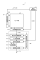
- FIG. 1 is a plan view illustrating a detection device according to a first embodiment.
- FIG. 2 is a block diagram showing an example of the configuration of the detection device according to the first embodiment.
- FIG. 3 is a circuit diagram showing the detection device according to the first embodiment.
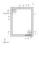
- FIG. 4 is a plan view showing a schematic configuration of a lower electrode, a lower buffer layer, an active layer, an upper buffer layer, and an upper electrode of a plurality of photodiodes.
- FIG. 5 is a cross-sectional view taken along line V-V' of FIG.
- FIG. 6 is a cross-sectional view taken along line VI-VI' of FIG.
- FIG. 7 is an explanatory diagram that illustrates a manufacturing process of the detection device according to the first embodiment.
- FIG. 8 is an explanatory diagram showing an enlarged view of steps ST1 and ST2 in FIG.
- FIG. 9 is an explanatory diagram illustrating a manufacturing process of the detection device according to the second embodiment.
- the term "on top” is used, unless otherwise specified, to include both a case in which another structure is placed directly on top of a structure so as to be in contact with the structure, and a case in which another structure is placed above a structure via yet another structure.
- First Embodiment Fig. 1 is a plan view showing a detection device according to the first embodiment.
- the detection device 1 has a substrate 21, a sensor unit 10, a gate line driving circuit 15, a signal line selection circuit 16, a detection circuit 48, a control circuit 122, a power supply circuit 123, a first light source substrate 51, a second light source substrate 52, and light sources 53 and 54.
- the first light source substrate 51 is provided with a plurality of light sources 53.
- the second light source substrate 52 is provided with a plurality of light sources 54.
- the control board 121 is electrically connected to the board 21 via the wiring board 71.
- the wiring board 71 is, for example, a flexible printed circuit board or a rigid board.
- the detection circuit 48 is provided on the wiring board 71.
- the control board 121 is provided with a control circuit 122 and a power supply circuit 123.
- the control circuit 122 is, for example, an FPGA (Field Programmable Gate Array).
- the control circuit 122 supplies control signals to the sensor unit 10, the gate line driving circuit 15, and the signal line selection circuit 16 to control the detection operation of the sensor unit 10.
- the control circuit 122 also supplies control signals to the light sources 53 and 54 to control the lighting or non-lighting of the light sources 53 and 54.
- the power supply circuit 123 supplies voltage signals such as a sensor power supply signal VDDSNS (see FIG. 3) to the sensor unit 10, the gate line driving circuit 15, and the signal line selection circuit 16. In addition, the power supply circuit 123 supplies power supply voltage to the light sources 53 and 54.
- VDDSNS sensor power supply signal
- the substrate 21 has a detection area AA and a peripheral area GA.
- the detection area AA is an area in which the multiple photodiodes PD (see FIG. 4) of the sensor unit 10 are provided.
- the peripheral area GA is an area between the outer periphery of the detection area AA and the outer edge of the substrate 21, and is an area in which the multiple photodiodes PD are not provided.
- the gate line driving circuit 15 and the signal line selection circuit 16 are provided in the peripheral area GA. Specifically, the gate line driving circuit 15 is provided in a region of the peripheral area GA that extends along the second direction Dy. The signal line selection circuit 16 is provided in a region of the peripheral area GA that extends along the first direction Dx, and is provided between the sensor unit 10 and the detection circuit 48.
- the first direction Dx is a direction in a plane parallel to the substrate 21.
- the second direction Dy is a direction in a plane parallel to the substrate 21, and is a direction perpendicular to the first direction Dx.
- the second direction Dy may intersect the first direction Dx without being perpendicular to it.
- the third direction Dz is a direction perpendicular to the first direction Dx and the second direction Dy, and is the normal direction of the main surface of the substrate 21.
- plane view refers to the positional relationship when viewed from a direction perpendicular to the substrate 21.
- the multiple light sources 53 are provided on the first light source substrate 51 and are arranged along the second direction Dy.
- the multiple light sources 54 are provided on the second light source substrate 52 and are arranged along the second direction Dy.
- the first light source substrate 51 and the second light source substrate 52 are electrically connected to the control circuit 122 and the power supply circuit 123 via terminal portions 124 and 125, respectively, provided on the control board 121.
- the multiple light sources 53 and the multiple light sources 54 may be, for example, inorganic light-emitting diodes (LEDs) or organic light-emitting diodes (OLEDs).
- the multiple light sources 53 and the multiple light sources 54 each emit light of a different wavelength.
- the first light emitted from the light source 53 is mainly reflected by the surface of the object to be detected, such as a finger, and enters the sensor unit 10. This allows the sensor unit 10 to detect a fingerprint by detecting the uneven shape of the surface of the finger.
- the second light emitted from the light source 54 is mainly reflected inside the finger or passes through the finger and enters the sensor unit 10. This allows the sensor unit 10 to detect information about a living body inside the finger.
- Information about a living body includes, for example, the pulse waves, pulse, and blood vessel images of the finger or palm.
- the detection device 1 may be configured as a fingerprint detection device that detects fingerprints, or a vein detection device that detects blood vessel patterns such as veins.
- the detection device 1 is provided with multiple types of light sources 53, 54 as light sources. However, this is not limited to this, and there may be only one type of light source. For example, multiple light sources 53 and multiple light sources 54 may be arranged on each of the first light source substrate 51 and the second light source substrate 52. Furthermore, there may be one or three or more light source substrates on which the light sources 53 and the light sources 54 are arranged. Alternatively, it is sufficient that at least one or more light sources are arranged.
- FIG. 2 is a block diagram showing an example of the configuration of a detection device according to an embodiment.
- the detection device 1 further includes a detection control circuit 11 and a detection unit 40. Some or all of the functions of the detection control circuit 11 are included in the control circuit 122. In addition, some or all of the functions of the detection unit 40 other than the detection circuit 48 are included in the control circuit 122.
- the sensor unit 10 has multiple photodiodes PD.
- the photodiodes PD of the sensor unit 10 output an electrical signal corresponding to the irradiated light as a detection signal Vdet to the signal line selection circuit 16.
- the sensor unit 10 also performs detection according to the gate drive signal VGL supplied from the gate line drive circuit 15.
- the detection control circuit 11 is a circuit that supplies control signals to the gate line drive circuit 15, the signal line selection circuit 16, and the detection unit 40, respectively, and controls their operation.
- the detection control circuit 11 supplies various control signals, such as a start signal STV and a clock signal CK, to the gate line drive circuit 15.
- the detection control circuit 11 also supplies various control signals, such as a selection signal ASW, to the signal line selection circuit 16.
- the detection control circuit 11 also supplies various control signals to the light sources 53 and 54, controlling their lighting and non-lighting.
- the gate line driving circuit 15 is a circuit that drives multiple gate lines GL (see FIG. 3) based on various control signals.
- the gate line driving circuit 15 selects multiple gate lines GL sequentially or simultaneously, and supplies a gate driving signal VGL to the selected gate lines GL. In this way, the gate line driving circuit 15 selects multiple photodiodes PD connected to the gate lines GL.
- the signal line selection circuit 16 is a switch circuit that sequentially or simultaneously selects multiple signal lines SL (see FIG. 3).
- the signal line selection circuit 16 is, for example, a multiplexer.
- the signal line selection circuit 16 connects the selected signal line SL to the detection circuit 48 based on the selection signal ASW supplied from the detection control circuit 11. As a result, the signal line selection circuit 16 outputs the detection signal Vdet of the photodiode PD to the detection unit 40.
- the detection unit 40 includes a detection circuit 48, a signal processing circuit 44, a coordinate extraction circuit 45, a memory circuit 46, and a detection timing control circuit 47.
- the detection timing control circuit 47 controls the detection circuit 48, the signal processing circuit 44, and the coordinate extraction circuit 45 to operate in synchronization based on a control signal supplied from the detection control circuit 11.
- the detection circuit 48 is, for example, an analog front-end circuit (AFE).
- the detection circuit 48 is a signal processing circuit having at least the functions of a detection signal amplifier circuit 42 and an A/D conversion circuit 43.
- the detection signal amplifier circuit 42 amplifies the detection signal Vdet.
- the A/D conversion circuit 43 converts the analog signal output from the detection signal amplifier circuit 42 into a digital signal.
- the signal processing circuit 44 is a logic circuit that detects a predetermined physical quantity input to the sensor unit 10 based on the output signal of the detection circuit 48. When a finger is in contact with or close to the detection surface, the signal processing circuit 44 can detect unevenness on the surface of the finger or palm based on the signal from the detection circuit 48. The signal processing circuit 44 can also detect information about the living body based on the signal from the detection circuit 48. The information about the living body is, for example, an image of the blood vessels in the finger or palm, pulse waves, pulse rate, blood oxygen concentration, etc.
- the memory circuit 46 temporarily stores the signal calculated by the signal processing circuit 44.
- the memory circuit 46 may be, for example, a RAM (Random Access Memory), a register circuit, etc.
- the coordinate extraction circuit 45 is a logic circuit that determines the detection coordinates of the unevenness of the surface of a finger, etc., when the signal processing circuit 44 detects contact or proximity of a finger.
- the coordinate extraction circuit 45 is also a logic circuit that determines the detection coordinates of the blood vessels of the finger or palm.
- the coordinate extraction circuit 45 combines the detection signals Vdet output from each photodiode PD of the sensor unit 10 to generate two-dimensional information indicating the shape of the unevenness of the surface of the finger, etc., and two-dimensional information indicating the shape of the blood vessels of the finger or palm.
- the coordinate extraction circuit 45 may output the detection signal Vdet as the sensor output voltage Vo without calculating the detection coordinates.
- FIG. 3 is a circuit diagram showing a detection device according to an embodiment. Note that FIG. 3 also shows the circuit configuration of a detection circuit 48.
- a sensor pixel PX includes a photodiode PD, a capacitance element Ca, and a drive transistor Tr.
- the capacitance element Ca is a capacitance (sensor capacitance) formed in the photodiode PD, and is equivalently connected in parallel with the photodiode PD.
- FIG. 3 of the multiple gate lines GL, two gate lines GL(m) and GL(m+1) aligned in the second direction Dy are shown. Also, of the multiple signal lines SL, two signal lines SL(n) and SL(n+1) aligned in the first direction Dx are shown.
- the sensor pixel PX is the area surrounded by the gate line GL and the signal line SL.
- the drive transistor Tr is provided corresponding to each of the multiple photodiodes PD.
- the drive transistor Tr is composed of a thin film transistor, and in this example, is composed of an n-channel MOS (Metal Oxide Semiconductor) type TFT (Thin Film Transistor).
- Each of the multiple gate lines GL is connected to the gates of multiple drive transistors Tr arranged in a first direction Dx.
- Each of the multiple signal lines SL is connected to one of the sources and drains of multiple drive transistors Tr arranged in a second direction Dy.
- the other of the sources and drains of the multiple drive transistors Tr is connected to the cathode of the photodiode PD and the capacitance element Ca.
- the anode of the photodiode PD is supplied with a sensor power supply signal VDDSNS from the power supply circuit 123 (see FIG. 1).
- the signal line SL and the capacitance element Ca are supplied with a sensor reference voltage COM, which is the initial potential of the signal line SL and the capacitance element Ca, from the power supply circuit 123 via the reset transistor TrR.
- the switch SSW of the detection circuit 48 is turned on and connected to the signal line SL.
- the detection signal amplifier circuit 42 of the detection circuit 48 converts the current or charge supplied from the signal line SL into a voltage corresponding to the current or charge.
- a reference potential (Vref) having a fixed potential is input to the non-inverting input section (+) of the detection signal amplifier circuit 42, and the signal line SL is connected to the inverting input section (-).
- a signal equal to the sensor reference voltage COM is input as the reference potential (Vref) voltage.
- the control circuit 122 see FIG.
- the detection signal amplifier circuit 42 also has a capacitance element Cb and a reset switch RSW. During the reset period, the reset switch RSW is turned on and the charge of the capacitance element Cb is reset.
- the driving transistor Tr is not limited to an n-type TFT, and may be a p-type TFT.
- the pixel circuit of the sensor pixel PX shown in FIG. 3 is merely an example, and the sensor pixel PX may be provided with multiple transistors corresponding to one photodiode PD.
- Figure 4 is a plan view that shows a schematic configuration of the lower electrode, lower buffer layer, active layer, upper buffer layer, and upper electrode of multiple photodiodes.
- multiple photodiodes PD (organic photosensors) are arranged in a matrix in the detection area AA.
- the multiple photodiodes PD have a lower electrode 31, a lower buffer layer 32, an active layer 33, an upper buffer layer 34, an upper metal layer 35M, and an upper electrode 35.
- the multiple lower electrodes 31 are provided separately for each of the multiple photodiodes PD and are arranged in a matrix in the detection area AA.
- the lower buffer layer 32, the active layer 33, the upper buffer layer 34, and the upper metal layer 35M are provided continuously across the multiple photodiodes PD and are provided throughout the entire detection area AA.
- the upper electrode 35 is provided continuously across multiple photodiodes PD, and is provided in the detection area AA and the peripheral area GA.
- the upper electrode 35 is provided to cover the lower buffer layer 32, the active layer 33, the upper buffer layer 34, and the upper metal layer 35M.
- the outer edge of the upper electrode 35 is located outside (toward the outer edge of the substrate 21) the outer edges of the lower buffer layer 32, the active layer 33, the upper buffer layer 34, and the upper metal layer 35M.
- a part of the upper electrode 35 is connected to a contact portion CN provided in the peripheral area GA, and is electrically connected to an external circuit (for example, the control circuit 122 or the power supply circuit 123 (see FIG. 1)) through wiring on the substrate 21.
- the detection device 1 has a sealing film 90 that covers the multiple photodiodes PD.
- the sealing film 90 is provided across the detection area AA and the peripheral area GA, and is provided up to the outer edge side of the substrate 21.
- the sealing film 90 is provided to cover the multiple photodiodes PD.
- the outer edge of the sealing film 90 is located outside the outer edge of the upper electrode 35 (on the outer edge side of the substrate 21).
- the wiring board 71 (see FIG. 1) is not shown in FIG. 4, the wiring board 71 is connected to a terminal provided on the substrate 21 outside the upper electrode 35.
- the sealing film 90 may have an opening at the connection point between the wiring board 71 and the terminal, if necessary.
- Figure 5 is a cross-sectional view taken along line V-V' in Figure 4.
- Figure 6 is a cross-sectional view taken along line VI-VI' in Figure 4.
- the direction perpendicular to the surface of the substrate 21, from the substrate 21 toward the sealing film 90 is referred to as the "upper side” or simply “upper”.
- the direction from the sealing film 90 toward the substrate 21 is referred to as the "lower side” or simply “lower”.
- the detection device 1 has a substrate 21, a TFT layer 22, an organic insulating film 26, a barrier film 27, a photodiode PD, and a sealing film 90.
- the TFT layer 22, the organic insulating film 26, the barrier film 27, the photodiode PD, and the sealing film 90 are stacked in this order on the substrate 21.
- the substrate 21 is an insulating substrate formed from a film-like resin.
- the TFT layer 22 is a circuit formation layer in which the pixel circuits of the sensor pixels PX (see FIG. 3) are formed.
- the TFT layer 22 includes various wiring such as the drive transistors Tr, gate lines GL, and signal lines SL, as well as multiple inorganic insulating films that provide insulation between layers.
- the organic insulating film 26 is provided to cover the drive transistor Tr formed in the TFT layer 22.
- the organic insulating film 26 is a planarization film formed from an organic insulating material.
- the barrier film 27 is provided on the organic insulating film 26.
- the barrier film 27 is formed from an inorganic insulating material such as a silicon nitride film (SiN).
- the photodiode PD is provided on the barrier film 27.
- the photodiode PD is stacked in the following order, perpendicular to the substrate 21: lower electrode 31, lower buffer layer 32, active layer 33, upper buffer layer 34, upper metal layer 35M, and upper electrode 35.
- the photodiode PD of this embodiment is an organic photodiode (OPD) that uses an organic semiconductor as the active layer 33.
- OPD organic photodiode
- the lower electrode 31 is formed of a conductive material having light transmissivity, such as ITO (Indium Tin Oxide).
- the lower buffer layer 32, the active layer 33, the upper buffer layer 34, the upper metal layer 35M, and the upper electrode 35 are provided continuously across multiple photodiodes PD. Specifically, the lower buffer layer 32, the active layer 33, the upper buffer layer 34, the upper metal layer 35M, and the upper electrode 35 are provided overlapping the lower electrode 31, and are also provided in the region between adjacent lower electrodes 31.
- the insulating film 36 is provided to cover the periphery of the lower electrode 31.
- the insulating film 36 insulates the lower electrodes 31 of adjacent photodiodes PD. Even if a step occurs in the lower buffer layer 32 at the periphery of the lower electrode 31, the insulating film 36 is provided, so that the occurrence of a short circuit between the active layer 33 and the lower electrode 31 can be suppressed.
- the insulating film 36 is formed of an inorganic insulating material such as a silicon nitride film (SiN) or a silicon oxide film (SiO 2 ).
- the insulating film 36 is provided to cover the periphery of the contact portion CN.
- the insulating film 36 is provided to cover the entire barrier film 27, but is not limited thereto, and may be provided to cover at least the periphery of the lower electrode 31 and the periphery of the contact portion CN.
- the active layer 33 changes its characteristics (for example, voltage-current characteristics and resistance value) depending on the light irradiated thereto.
- An organic material is used as the material of the active layer 33.
- the active layer 33 has a bulk heterostructure in which a p-type organic semiconductor and an n-type fullerene derivative (PCBM) which is an n-type organic semiconductor are mixed.
- PCBM n-type fullerene derivative
- low molecular weight organic materials such as C 60 (fullerene), PCBM (phenyl C 61 -butyric acid methyl ester), CuPc (copper phthalocyanine), F 16 CuPc (fluorinated copper phthalocyanine) , rubrene (5,6,11,12-tetraphenyltetracene), and PDI (perylene derivative) can be used as the active layer 33.
- C 60 fulllerene
- PCBM phenyl C 61 -butyric acid methyl ester
- CuPc copper phthalocyanine
- F 16 CuPc fluorinated copper phthalocyanine
- rubrene 5,6,11,12-tetraphenyltetracene
- PDI perylene derivative
- the active layer 33 can be formed by a deposition type (dry process) using these low molecular weight organic materials.
- the active layer 33 may be, for example, a laminated film of CuPc and F 16 CuPc, or a laminated film of rubrene and C 60.
- the active layer 33 can also be formed by a coating type (wet process).
- the active layer 33 is made of a material that combines the above-mentioned low molecular weight organic material and a polymer organic material.
- the polymer organic material for example, P3HT (poly(3-hexylthiophene)), F8BT (F8-alt-benzothiadiazole), etc. can be used.
- the active layer 33 can be a film in a state where P3HT and PCBM are mixed, or a film in a state where F8BT and PDI are mixed.
- the active layer 33 is not limited to a bulk heterostructure and may be a PIN type.
- the lower buffer layer 32 and the upper buffer layer 34 are provided to facilitate the holes and electrons generated in the active layer 33 reaching the lower electrode 31 or the upper electrode 35.
- the lower buffer layer 32 is provided between the lower electrode 31 and the active layer 33, and is in direct contact with the lower electrode 31 and the active layer 33.
- the lower buffer layer 32 is also provided between adjacent lower electrodes 31, covering the barrier film 27 and the insulating film 36.
- the upper buffer layer 34 is provided between the active layer 33 and the upper electrode 35.
- the upper metal layer 35M is provided between the upper buffer layer 34 and the upper electrode 35.
- the upper buffer layer 34 is in direct contact with the active layer 33 and the upper metal layer 35M.
- the lower electrode 31 is the cathode electrode of the photodiode PD
- the upper electrode 35 is the anode electrode of the photodiode PD
- the lower buffer layer 32 is an electron transport layer
- the upper buffer layer 34 is a hole transport layer.
- the material of the electron transport layer is ethoxylated polyethyleneimine (PEIE).
- PEIE polyethyleneimine
- the material of the hole transport layer is a metal oxide layer.
- tungsten oxide (WO 3 ), molybdenum oxide, or the like is used as the metal oxide layer.
- the lower electrode 31 may be the anode electrode of the photodiode PD, and the upper electrode 35 may be the cathode electrode of the photodiode PD.
- the lower buffer layer 32 may be a hole transport layer, and the upper buffer layer 34 may be an electron transport layer.
- the upper metal layer 35M is formed to have the same width (area) as the lower buffer layer 32, the active layer 33, and the upper buffer layer 34.
- the upper metal layer 35M functions as the upper electrode of the photodiode PD and also functions as a mask when patterning the lower buffer layer 32, the active layer 33, and the upper buffer layer 34.
- the manufacturing process of the photodiode PD will be described later with reference to FIG. 7.
- the side surfaces of the photodiode PD are shown as being perpendicular to the surface of the substrate 21.
- the side surfaces 32s, 33s, 34s, and 35Ms of the photodiode PD have a forward tapered shape (see the enlarged view in Figure 8).
- the upper electrode 35 covers the top surface of the upper metal layer 35M, as well as the side surface 32s of the lower buffer layer 32, the side surface 33s of the active layer 33, the side surface 34s of the upper buffer layer 34, and the side surface 35Ms of the upper metal layer 35M.
- side surface 32s of the lower buffer layer 32, side surface 33s of the active layer 33, side surface 34s of the upper buffer layer 34, and side surface 35Ms of the upper metal layer 35M may be referred to as "side surfaces 32s, 33s, 34s, 35Ms of the photodiode PD.”
- the upper electrode 35 includes an overlapping portion 35a, a side portion 35b, and an extending portion 35c.
- the overlapping portion 35a covers the upper surface of the upper metal layer 35M.
- the side portion 35b covers the side surfaces 32s, 33s, 34s, and 35Ms of the photodiode PD.
- the upper end of the side portion 35b is connected to the overlapping portion 35a, and the lower end of the side portion 35b is connected to the extending portion 35c.
- the extending portion 35c extends to the peripheral area GA outside the side surfaces 32s, 33s, 34s, and 35Ms of the multiple photodiodes PD.
- the extending portion 35c of the upper electrode 35 is provided on the barrier film 27 and the insulating film 36 in a region that does not overlap with the multiple photodiodes PD.
- the side surface 35s on the outer edge of the upper electrode 35 (side surface 35s of extension portion 35c) is located closer to the outer edge of the substrate 21 than the side surfaces 32s, 33s, 34s, 35Ms of the multiple photodiodes PD.
- the planar area of the upper electrode 35 is larger than the planar areas of the lower buffer layer 32, the active layer 33, the upper buffer layer 34, and the upper metal layer 35M.
- the side surface 35s of the upper electrode 35 is located closer to the detection area AA than the side surface of the barrier film 27. Also, as shown in FIG. 6, a portion of the extension portion 35c of the upper electrode 35 extends to an area overlapping with the contact portion CN and is connected to the contact portion CN.
- the upper electrode 35 is formed of a conductive material having translucency, such as ITO or IZO. Without being limited thereto, the upper electrode 35 may be formed of a conductive material having no translucency, such as silver (Ag).
- the upper metal layer 35M is formed of a metal material, such as silver (Ag). In other words, the upper metal layer 35M may be made of the same metal material as the upper electrode 35.
- the sealing film 90 is provided to cover the multiple photodiodes PD.
- the sealing film 90 is provided to cover the overlapping portion 35a, side portion 35b, and extension portion 35c of the upper electrode 35.
- the side surface of the sealing film 90 is located closer to the outer edge of the substrate 21 than the side surface 35s on the outer edge side of the upper electrode 35.
- the sealing film 90 effectively seals the photodiodes PD and can prevent moisture from entering from the outside.
- the sealing film 90 covers the side surface 35s on the outer edge side of the upper electrode 35, it can effectively prevent moisture from entering from the outer edge side of the substrate 21 compared to when the upper electrode 35 extends to the outer edge side of the substrate 21.
- the sealing film 90 is formed of an inorganic film such as a silicon nitride film or an aluminum oxide film.
- the sealing film 90 is not limited to a single layer film, but may be a laminated film in which multiple inorganic films are stacked. Alternatively, the sealing film 90 may be a laminated film in which an organic film formed of a resin film such as acrylic and an inorganic film are stacked.
- the side surfaces 32s, 33s, 34s, and 35Ms of the lower buffer layer 32, active layer 33, upper buffer layer 34, and upper metal layer 35M are covered with the upper electrode 35. This makes it possible to suppress contact between the patterning mask and the active layer 33 when forming the upper electrode 35, compared to when the upper electrode 35 is formed in the same shape as the lower buffer layer 32, active layer 33, and upper buffer layer 34.
- Fig. 7 is an explanatory diagram that shows a schematic diagram of the manufacturing process of the detection device according to the first embodiment.
- Fig. 8 is an explanatory diagram that shows an enlarged view of steps ST1 and ST2 in Fig. 7. Note that in Fig. 7, the lower buffer layer 32 and the upper buffer layer 34 are omitted in order to make the drawing easier to see.
- a TFT layer 22, an organic insulating film 26, and a barrier film 27 are formed on a substrate 21.
- the lower electrode 31 is patterned in a matrix shape corresponding to the arrangement of the multiple photodiodes PD.
- the lower buffer layer 32, the active layer 33, and the upper buffer layer 34 are formed over the entire surface of the substrate 21, across the detection area AA and the peripheral area GA.
- a film forming device uses a first patterning mask 201 to form an upper metal layer 35M on the upper buffer layer 34 in an area corresponding to the detection area AA of the substrate 21 (step ST1).
- the first patterning mask 201 for forming the upper metal layer 35M is a metal mask having an opening OP1.
- the opening OP1 is provided at a position overlapping with the area (detection area AA) where multiple photodiodes PD are to be formed.
- the upper metal layer 35M is formed by sputtering, vapor deposition, plasma CVD, or the like.
- the first patterning mask 201 is positioned above and spaced apart from the upper buffer layer 34.
- the upper metal layer 35M is deposited around the opening OP1 of the first patterning mask 201 to the outside.
- the side surface 35Ms of the upper metal layer 35M is formed to have a forward tapered shape.
- the lower buffer layer 32, the active layer 33, and the upper buffer layer 34 are removed from the regions where the upper metal layer 35M is not provided (step ST2).
- the upper metal layer 35M is used as a mask.
- the lower buffer layer 32, the active layer 33, and the upper buffer layer 34 in the regions that do not overlap with the upper metal layer 35M are removed by dry etching.
- the lower buffer layer 32, the active layer 33, and the upper buffer layer 34 in the regions that overlap with the upper metal layer 35M are formed as a plurality of photodiodes PD.
- etching of the lower buffer layer 32, the active layer 33, and the upper buffer layer 34 first proceeds in the region outside the side surface 35Ms of the upper metal layer 35M.
- the thin outer edge portion the portion overlapping the side surface 35Ms of the upper metal layer 35M is also etched.
- step ST2b of FIG. 8 when the outer edge portion of the upper metal layer 35M is further removed, etching of the lower buffer layer 32, active layer 33, and upper buffer layer 34 proceeds sequentially in the areas overlapping with the removed portion of the upper metal layer 35M.
- the side surfaces 32s, 33s, and 34s of the lower buffer layer 32, active layer 33, and upper buffer layer 34 of the photodiode PD are formed to have a forward tapered shape.
- the side surface 35Ms of the upper metal layer 35M is also formed to have a forward tapered shape.
- a film forming apparatus uses a second patterning mask 202 to form an upper electrode 35 on the upper metal layer 35M (step ST3).
- the second patterning mask 202 for forming the upper electrode 35 is a metal mask having an opening OP2.
- the opening OP2 of the second patterning mask 202 has a width W2 that is at least greater than the width W1 of the active layer 33.
- the width W1 of the active layer 33 is the maximum width between the side surfaces 33s of the active layer 33.
- the active layer 33 has a forward tapered shape, and the maximum width W1 of the active layer 33 is the distance at the portion where the lower end of the side surface 33s of the active layer 33 contacts the insulating film 36 or the barrier film 27.
- the distance L1 between the inner wall of the opening OP2 of the second patterning mask 202 and the side surface 33s of the active layer 33 is 500 ⁇ m or more. More specifically, the distance L1 is the distance between the inner wall of the opening OP2 of the second patterning mask 202 and the lower end of the side surface 33s of the active layer 33, which contacts the insulating film 36 or the barrier film 27, in a direction parallel to the surface of the substrate 21. The distance L1 is different for each side of the photodiode PD depending on the alignment accuracy of the second patterning mask 202. For example, as shown in FIG.
- the distance L1 between the inner wall of the opening OP2 and the side surface 33s of the active layer 33 is larger than the distance L1 on the opposite side.
- the second patterning mask 202 is arranged so that the minimum distance L1 among the distances L1 along the outer edge of the photodiode PD is 500 ⁇ m or more.
- the width W2 of the opening OP2 is smaller than the width of the barrier film 27 formed on the substrate 21.
- the inner wall of the opening OP2 of the second patterning mask 202 overlaps with the outer edge side of the barrier film 27 formed on the substrate 21.
- the upper electrode 35 is formed to cover the top surface of the upper metal layer 35M, as well as the side surfaces 32s, 33s, 34s of the photodiode PD and the side surface 35Ms of the upper metal layer 35M.
- the upper electrode 35 is provided extending further to the outer edge side of the substrate 21 than the side surface 33s of the active layer 33.
- the side surface 35s on the outer edge side of the upper electrode 35 is formed inside (towards the detection area AA) than the side surface of the barrier film 27.
- a film forming device forms a sealing film 90 covering the upper electrode 35 (step ST4).
- a patterning mask (not shown) for forming the sealing film 90 has an opening with a width larger than the opening OP2.
- the sealing film 90 is formed covering the entire surface of the upper electrode 35.
- the side surface 35s on the outer edge side of the upper electrode 35 is also covered by the sealing film 90.
- the side surface 35s on the outer edge side of the upper electrode 35 is formed inside (towards the detection area AA) more than the side surface of the sealing film 90.
- the detection device 1 of this embodiment is formed by the above-mentioned process.
- the inner wall of the opening OP2 of the second patterning mask 202 is positioned at a predetermined distance L1 from the side surface 33s of the active layer 33. This makes it possible to suppress contact between the second patterning mask 202 and the side surface 33s of the active layer 33, compared to when the upper electrode 35 is formed in the same shape as the lower buffer layer 32, the active layer 33, and the upper buffer layer 34, i.e., when the side surface 35s of the upper electrode 35 is provided at a position overlapping the side surfaces 32s, 33s, 34s, and 35Ms of the photodiode PD.
- the manufacturing process of the detection device 1 shown in Figures 7 and 8 is merely a schematic illustration and can be modified as appropriate.
- the layered structure and forward tapered shapes of the side surfaces 32s, 33s, and 34s shown in Figure 8 are shown exaggerated to make it easier to understand, and the film thickness, inclination, width, etc. of the side surfaces 32s, 33s, and 34s may be different.
- Second Embodiment 9 is an explanatory diagram showing a manufacturing process of the detection device according to the second embodiment.
- the same components as those described in the above embodiment are denoted by the same reference numerals, and duplicated description will be omitted.
- the lower buffer layer 32 and the upper buffer layer 34 are omitted, as in FIG. 7.
- the manufacturing process shown in FIG. 9 corresponds to the process (step ST3) of forming the upper electrode 35 in FIG. 7.
- the processes of depositing the upper metal layer 35M, removing the active layer 33, and depositing the sealing film 90 are similar to the processes of steps ST1, ST2, and ST4 described above in FIG. 7, and repeated explanations will be omitted.
- the second patterning mask 202 is supported on spacers 203 provided on the outer edge side of the substrate 21.
- the height of the spacers 203 is greater than the total height of the lower buffer layer 32, the active layer 33, the upper buffer layer 34, and the upper metal layer 35M.
- the spacers 203 are resin tapes made of a resin material such as polyimide.
- the second patterning mask 202 is disposed above the upper metal layer 35M. More specifically, in the direction perpendicular to the substrate 21, the lower surface of the second patterning mask 202 is disposed at a distance from the upper surface of the upper metal layer 35M.
- the width W2 of the opening OP2 of the second patterning mask 202 is at least greater than the width W1 of the active layer 33.
- the inner wall of the opening OP2 of the second patterning mask 202 may be positioned so as to overlap the side surface 33s of the active layer 33.
- the distance L1 (see FIG. 7) between the inner wall of the opening OP2 of the second patterning mask 202 and the side surface 33s of the active layer 33 may be 500 ⁇ m or less.
- a film forming device uses the second patterning mask 202 to form the upper electrode 35 on the upper metal layer 35M (step ST3A).
- the upper electrode 35 is formed between the lower surface of the second patterning mask 202 and the upper surface of the upper metal layer 35M.
- the upper electrode 35 is formed to cover the upper surface of the upper metal layer 35M, as well as the side surfaces 32s, 33s, and 34s of the photodiode PD and the side surface 35Ms of the upper metal layer 35M.
- the second patterning mask 202 is supported by the spacers 203 during the deposition process of the upper electrode 35, so that contact between the second patterning mask 202 and the respective side surfaces 32s, 33s, and 34s of the lower buffer layer 32, active layer 33, and upper buffer layer 34 can be suppressed.
Landscapes
- Physics & Mathematics (AREA)
- Electromagnetism (AREA)
- Solid State Image Pick-Up Elements (AREA)
Priority Applications (1)
| Application Number | Priority Date | Filing Date | Title |
|---|---|---|---|
| JP2025527568A JPWO2024262191A1 (https=) | 2023-06-20 | 2024-05-14 |
Applications Claiming Priority (2)
| Application Number | Priority Date | Filing Date | Title |
|---|---|---|---|
| JP2023100536 | 2023-06-20 | ||
| JP2023-100536 | 2023-06-20 |
Publications (1)
| Publication Number | Publication Date |
|---|---|
| WO2024262191A1 true WO2024262191A1 (ja) | 2024-12-26 |
Family
ID=93935534
Family Applications (1)
| Application Number | Title | Priority Date | Filing Date |
|---|---|---|---|
| PCT/JP2024/017755 Ceased WO2024262191A1 (ja) | 2023-06-20 | 2024-05-14 | 検出装置及び検出装置の製造方法 |
Country Status (2)
| Country | Link |
|---|---|
| JP (1) | JPWO2024262191A1 (https=) |
| WO (1) | WO2024262191A1 (https=) |
Citations (5)
| Publication number | Priority date | Publication date | Assignee | Title |
|---|---|---|---|---|
| JP2006049874A (ja) * | 2004-07-06 | 2006-02-16 | Fuji Photo Film Co Ltd | 機能素子及びその製造方法 |
| JP2015056554A (ja) * | 2013-09-12 | 2015-03-23 | ソニー株式会社 | 固体撮像素子および製造方法、並びに電子機器 |
| WO2017061176A1 (ja) * | 2015-10-06 | 2017-04-13 | ソニー株式会社 | 固体撮像素子および固体撮像素子の製造方法 |
| JP2022094304A (ja) * | 2019-10-04 | 2022-06-24 | 株式会社半導体エネルギー研究所 | 半導体装置 |
| JP2023012380A (ja) * | 2021-07-13 | 2023-01-25 | 株式会社ジャパンディスプレイ | 検出装置 |
-
2024
- 2024-05-14 WO PCT/JP2024/017755 patent/WO2024262191A1/ja not_active Ceased
- 2024-05-14 JP JP2025527568A patent/JPWO2024262191A1/ja active Pending
Patent Citations (5)
| Publication number | Priority date | Publication date | Assignee | Title |
|---|---|---|---|---|
| JP2006049874A (ja) * | 2004-07-06 | 2006-02-16 | Fuji Photo Film Co Ltd | 機能素子及びその製造方法 |
| JP2015056554A (ja) * | 2013-09-12 | 2015-03-23 | ソニー株式会社 | 固体撮像素子および製造方法、並びに電子機器 |
| WO2017061176A1 (ja) * | 2015-10-06 | 2017-04-13 | ソニー株式会社 | 固体撮像素子および固体撮像素子の製造方法 |
| JP2022094304A (ja) * | 2019-10-04 | 2022-06-24 | 株式会社半導体エネルギー研究所 | 半導体装置 |
| JP2023012380A (ja) * | 2021-07-13 | 2023-01-25 | 株式会社ジャパンディスプレイ | 検出装置 |
Also Published As
| Publication number | Publication date |
|---|---|
| JPWO2024262191A1 (https=) | 2024-12-26 |
Similar Documents
| Publication | Publication Date | Title |
|---|---|---|
| JP7220775B2 (ja) | 検出装置 | |
| JP7633109B2 (ja) | 検出装置 | |
| JP7751416B2 (ja) | 検出装置 | |
| US20250008759A1 (en) | Detection device | |
| JP7818127B2 (ja) | 検出装置 | |
| JP7645689B2 (ja) | 検出装置及び撮像装置 | |
| CN113711362A (zh) | 包括薄膜晶体管和有机光电二极管的图像传感器阵列器件 | |
| JP2026020189A (ja) | 電子機器 | |
| US12364091B2 (en) | Detection device | |
| JP7806101B2 (ja) | 検出装置 | |
| WO2024262191A1 (ja) | 検出装置及び検出装置の製造方法 | |
| JP7606941B2 (ja) | 検出装置 | |
| JP7684887B2 (ja) | 検出装置 | |
| WO2026042483A1 (ja) | 検出装置及び検出装置の製造方法 | |
| US20250255085A1 (en) | Detection device | |
| WO2026034159A1 (ja) | 検出装置及び検出装置の製造方法 | |
| WO2024257502A1 (ja) | 検出装置 | |
| WO2026048984A1 (ja) | 検出装置 | |
| WO2024135561A1 (ja) | 検出装置 | |
| WO2025105160A1 (ja) | 検出装置 | |
| JP2025148873A (ja) | 電子機器 | |
| WO2026053915A1 (ja) | 検出装置及び検出装置の製造方法 | |
| WO2024135768A1 (ja) | 検出装置 | |
| US12396102B2 (en) | Electronic device | |
| JP2024084351A (ja) | 検出装置及びその製造方法 |
Legal Events
| Date | Code | Title | Description |
|---|---|---|---|
| 121 | Ep: the epo has been informed by wipo that ep was designated in this application |
Ref document number: 24825600 Country of ref document: EP Kind code of ref document: A1 |
|
| ENP | Entry into the national phase |
Ref document number: 2025527568 Country of ref document: JP Kind code of ref document: A |
|
| WWE | Wipo information: entry into national phase |
Ref document number: 2025527568 Country of ref document: JP |
|
| NENP | Non-entry into the national phase |
Ref country code: DE |