WO2024262148A1 - 電気パルス発生装置 - Google Patents
電気パルス発生装置 Download PDFInfo
- Publication number
- WO2024262148A1 WO2024262148A1 PCT/JP2024/015212 JP2024015212W WO2024262148A1 WO 2024262148 A1 WO2024262148 A1 WO 2024262148A1 JP 2024015212 W JP2024015212 W JP 2024015212W WO 2024262148 A1 WO2024262148 A1 WO 2024262148A1
- Authority
- WO
- WIPO (PCT)
- Prior art keywords
- current
- capacitor
- electric pulse
- pulse generator
- switching element
- Prior art date
- Legal status (The legal status is an assumption and is not a legal conclusion. Google has not performed a legal analysis and makes no representation as to the accuracy of the status listed.)
- Ceased
Links
Images











Classifications
-
- H—ELECTRICITY
- H03—ELECTRONIC CIRCUITRY
- H03K—PULSE TECHNIQUE
- H03K3/00—Circuits for generating electric pulses; Monostable, bistable or multistable circuits
- H03K3/02—Generators characterised by the type of circuit or by the means used for producing pulses
- H03K3/53—Generators characterised by the type of circuit or by the means used for producing pulses by the use of an energy-accumulating element discharged through the load by a switching device controlled by an external signal and not incorporating positive feedback
- H03K3/57—Generators characterised by the type of circuit or by the means used for producing pulses by the use of an energy-accumulating element discharged through the load by a switching device controlled by an external signal and not incorporating positive feedback the switching device being a semiconductor device
-
- H—ELECTRICITY
- H05—ELECTRIC TECHNIQUES NOT OTHERWISE PROVIDED FOR
- H05B—ELECTRIC HEATING; ELECTRIC LIGHT SOURCES NOT OTHERWISE PROVIDED FOR; CIRCUIT ARRANGEMENTS FOR ELECTRIC LIGHT SOURCES, IN GENERAL
- H05B3/00—Ohmic-resistance heating
-
- H—ELECTRICITY
- H05—ELECTRIC TECHNIQUES NOT OTHERWISE PROVIDED FOR
- H05B—ELECTRIC HEATING; ELECTRIC LIGHT SOURCES NOT OTHERWISE PROVIDED FOR; CIRCUIT ARRANGEMENTS FOR ELECTRIC LIGHT SOURCES, IN GENERAL
- H05B47/00—Circuit arrangements for operating light sources in general, i.e. where the type of light source is not relevant
Definitions
- the present invention relates to an electric pulse generator that applies an electric pulse to an object.
- a flash lamp is a lamp that is primarily used as a heating light source, emitting light ranging from the visible to infrared ranges and irradiating an object with this light to heat it.
- the lamp emits an amount of light that corresponds to the waveform of the supplied current. Therefore, by controlling this current waveform, particularly the pulse width, it is possible to control the heating depth of the object. For example, by appropriately controlling the pulse width and peak value of the current waveform, it is possible to heat only the surface of the object while minimizing thermal damage to the object.
- the above-mentioned technology can be applied to heating a substrate in a semiconductor manufacturing process.
- the substrate is formed by laminating a plurality of semiconductor layers and insulating layers on an upper layer of a base wafer.
- an annealing process is performed to diffuse doped impurities.
- a flash lamp is used for this annealing process.
- the technology of selectively heating the area near the surface of an object can also be applied to recycling layered materials.
- Electrical products such as communication terminal devices and home appliances that are no longer in use may contain usable resources. From the perspective of resource conservation, such electrical products that are no longer in use are required to be collected by businesses, disassembled, and recycled. Traditionally, this type of work has often been done by disassembling by hand or physically dismantling using a crusher. However, such work requires a lot of manpower, and the quality of the parts after dismantling tends to be low, which reduces the percentage that can be recycled.
- Waste eligible for recycling includes those in which insulating materials or semiconductors are layered over conductive materials such as metals. More specific examples include composite materials in which an organic material is applied to a metallic material, composite materials in which paint is applied to a metallic material, composite materials in which an insulating material is attached or vapor-deposited onto a metallic material, etc.
- waste materials made of composite materials including metal materials can be recycled by crushing and burning them, and separating and extracting the necessary metals from the resulting combustion ash.
- this method may result in the metals being denatured into metal compounds or alloys, which requires subsequent processing, and also results in a large amount of CO2 emissions during combustion, which is problematic in terms of environmental impact.
- the extracted materials are subjected to chemical processing such as electrolysis, ion exchange, and chemical reaction, but high-purity materials are not separated and recovered from the beginning, which results in a large energy burden.
- Patent Document 1 a method has been proposed in which a lamp is indirectly used to heat a specific object, and the lighting pulse width of the lamp is shortened to selectively heat the object.
- Patent Document 2 a method has been proposed in which, rather than indirectly using a lamp, a pulse voltage is directly applied to the object to be recycled to selectively heat and dismantle it.
- Patent Document 1 describes how efforts are being made to shorten the lighting pulse width of flash lamps in order to reduce the energy input to the lamp and the power supply. It also describes that, in addition to semiconductor annealing applications, there is a demand for short-pulse light in fields such as modifying the surface of ceramic thin films and adhesive fixing of optical components by photocuring.
- Patent Document 1 does not make any detailed mention of short pulses. It is believed that short-term light irradiation of the object, in other words, short-term energy supply, is important in order to prevent the object from having a heating history. Short-term energy supply makes it possible to selectively raise the temperature of only the surface of the object (the side to which energy is supplied). On the other hand, in order to achieve the purpose of surface treatment of the object, etc., it is necessary to supply a sufficient amount of energy. To achieve the desired treatment in a short time, it is necessary to increase the energy per unit time, which may lead to excessive heating of the object and damage to the lamp.
- Patent Document 2 The technology described in Patent Document 2 is to separate the positive metal foil that constitutes the battery from the active material bonded to its surface by appropriately passing a pulse current through the current-carrying object.
- it is important to control the energy input to the binder, which is the object to be heated, by supplying a high peak current to the object to be electrified. This is exactly the same idea as the heating with a lamp mentioned above.
- Patent Documents 1 and 2 do not disclose a power supply device that can reproducibly generate a high pulse current in a short time.
- the present invention aims to provide an electric pulse generator that can generate a pulse current that exhibits a high current peak in a short period of time with high reproducibility in order to selectively heat the vicinity of the surface of an object to be heated.
- the electric pulse generating device is a device for applying an electric pulse to an electric current application object, a high voltage source and a load circuit section arranged to be able to apply an output voltage from the high voltage source;
- the load circuit section includes: The current passing object; A switching element connected in series to the current-carrying object; a capacitor disposed in a position capable of being charged based on an output voltage from the high voltage source when the high voltage source and the load circuit unit are electrically connected; a diode including an anode terminal and a cathode terminal; the load circuit unit forms a first closed circuit, which is a series circuit including the capacitor, the current-carrying object, and the switching element, when the switching element is in a conductive state; the anode terminal and the cathode terminal of the diode are each connected to two points on the first closed circuit,
- the present invention is characterized in that, at a point in time when the switching element is transitioned from a non-conducting state to a conducting state while the capacitor
- the load circuit section includes a capacitor, a switching element, and a diode.
- the switching element is connected in series with the object to be energized, and the capacitor is disposed in a position where it can be charged based on a voltage from a high voltage source.
- the load circuit section forms a series circuit (first closed circuit) including the capacitor, the object to be energized, and the switching element.
- the capacitor By connecting the high voltage source to the load circuit with the switching element in a non-conducting state, the capacitor is charged by the voltage from the high voltage source. After that, by making the switching element conductive with the high voltage source and the load circuit electrically disconnected, a high current derived from the charging voltage of the capacitor is supplied to the object to be energized via the switching element. Since the current flows immediately after the switching element is made conductive, this current exhibits a pulsed shape.
- the load circuit section is provided with a diode.
- This diode is arranged such that, when the switching element is transitioned from a non-conductive state to a conductive state while the capacitor is in a charged state, the connection point between the cathode terminal and the first closed circuit is electrically closer to the high potential terminal of the capacitor than the connection point between the anode terminal and the first closed circuit.
- the switching element when the switching element is in a charged state to pass a high current to the current-carrying object, the current derived from the charging voltage of the capacitor flows to the current-carrying object, and then the current bypasses the capacitor and flows through the diode.
- the capacitor does not transition from the charged state of the capacitor immediately before the switching element is turned on to a charged state of reverse polarity.
- the flow of an oscillating current whose polarity changes is suppressed in the first closed circuit.
- the current waveform will be an alternating current (AC) with damped oscillations over a period of several milliseconds, but by adding a diode, this will become a single pulse, and the overall period of current supply can also be reduced.
- AC alternating current
- the above-mentioned electric pulse generator can be applied to a flash lamp, as an example.
- the effect of supplying a pulse current to a flash lamp using the electric pulse generator of the present invention will be explained in comparison with the case where a conventional electric pulse generator is used.
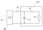
- FIG. 25 is a circuit diagram showing a schematic configuration of a conventional electric pulse generator used to light a flash lamp.
- a conventional electric pulse generator 100 includes a high voltage source 95 and a load circuit section to which the voltage generated from the high voltage source 95 is applied. More specifically, this load circuit section is formed of a closed circuit U100 including a capacitor 91, a mechanical switch 92, and an electric current object 90.
- the electric current object 90 corresponds to the flash lamp.
- the mechanical switch 92 is a switch that switches between energized and non-energized states by mechanical contact, but may also be a gap switch.
- the switching element 96 shown in FIG. 25 is provided for the purpose of switching the connection state between the high voltage source 95 and the capacitor 91.
- the switching element 96 When the switching element 96 is conductive, the capacitor 91 starts charging with the voltage output from the high voltage source 95.
- the switching element 96 is turned OFF and the mechanical switch 92 is turned ON, so that a high current derived from the charging voltage of the capacitor 91 is supplied to the current-carrying object 90.
- an AC current (damped oscillatory current) actually flows through the current passing object 90 for a period of about several tens of ms to 100 ms. This will be described later in the "Description of Embodiments" section with reference to FIG.
- a pulse current is supplied to the object 90 to be energized using the electric pulse generator 100 shown in FIG. 25, a current that exhibits a damped oscillatory waveform is actually supplied to the object 90 to be energized.
- the object 90 to be energized is a flash lamp
- the flash lamp irradiates the object to be heated with heating light (light with a wavelength absorbed by the object to be heated) over a certain length (the above-mentioned tens of ms to 100 ms).
- heat energy is supplied not only to the surface layer of the object to be heated, but also in the depth direction.
- the object to be heated is a wafer including a semiconductor layer, layers other than the outermost surface are also heated, raising concerns that this could affect the quality of the semiconductor.
- the object 90 to be energized is a flash lamp
- passing too high a current may damage the lamp.
- a high peak current may be supplied to the lamp for a short period of time to cause the lamp to discharge and emit light for a short period of time. To achieve this, it may seem as if it would be sufficient to simply prepare a high voltage source capable of generating and discharging a high voltage, for example on the order of kV.
- a current-carrying object is separated from another member from a composite member in which a current-carrying object as a conductive material is in contact with and integrated with another member by supplying a pulse current to the current-carrying object.
- a first member which is a thin-film conductor
- a second member made of a material with a lower conductivity than the first member
- a current with a short duration short pulse current
- the skin effect in which the current flows selectively on the surface of the conductor, can also be utilized.
- a high-frequency current it is possible to pass a high current intensively near the surface of the first member, in other words, near the interface between the first member and the second member, and instantly heat the region. From this perspective, it is preferable to supply a pulse current to the current-carrying object.
- Examples of the material of the first member include conductive materials such as copper, aluminum, iron, nickel, or alloys of these.
- Examples of the material of the second member include organic substances such as resins and paints, metal oxides, or insulating materials or semiconductors that are mixtures of these.
- the thin-film conductive portion of the electrified object may be overheated and destroyed or evaporated. This is thought to be because too much energy was supplied to the electrified object, and in this case it cannot be said that the first and second members have been separated.
- the input energy is defined as the value obtained by integrating the power over time.
- the time during which energy is supplied to the object to be heated can be set to a short and appropriate value, making it possible to supply energy to a limited range of the object to be heated and suppressing damage to both the part to be heated and the object to which electricity is passed.
- the switching elements constituting the load circuit section may be semiconductor elements.
- a switching element when a switching element is turned on to pass a current resulting from the high voltage charged in the capacitor to an electrified object, a high current flows instantaneously through the switching element. If the switching element is a mechanical element, the contacts of the switching element will wear out, causing the internal resistance of the switching element to change over time, and in some cases, opening and closing control may become impossible. For this reason, when different electrified objects are continuously dismantled, the accuracy of the dismantling may decrease over time.
- the switching element as a semiconductor element as described above, deterioration and wear over time are suppressed.
- semiconductor elements that can be used include thyristors and high-voltage IGBTs that have high voltage resistance.
- a load current flowing through the current-carrying object when the high voltage source and the load circuit unit are electrically connected includes a peak current and a ringing current that flows after the peak current and is less than 10% of a current value of the peak current,
- the load current may be configured to substantially taper off without changing polarity between the time when the peak current occurs and the time when the ringing current occurs.
- the load current has a main pulse width, which is the time width from the occurrence of the peak current to the occurrence of the ringing current, of 1.2 ms or less.
- the load circuit section includes an inductor
- the first closed circuit may be a series circuit including the capacitor, the current-carrying object, the switching element, and the inductor.
- the load circuit section may form a second closed circuit that includes the diode, the inductor, and the current-carrying object connected in series after the capacitor is discharged, but does not include the capacitor.
- the load circuit section may form a second closed circuit after the capacitor is discharged, including the diode and the inductor connected in series, and not including the capacitor or the current-carrying object.
- the dismantling device of the present invention makes it possible to expand the range of voltage applied to the high-voltage source required to maintain a high recovery rate of resources contained in the object.
- FIG. 1 is a circuit block diagram illustrating a schematic diagram of an electric pulse generator according to a first embodiment.
- 1 is a diagram showing an example of a flash lamp as an object to be energized;
- 1 is an example of a cross-sectional view of a composite structure in which an object to be electrically conducted and an object to be heated are integrated.
- 1 is an example of a cross-sectional view of a composite structure in which an object to be electrically conducted and an object to be heated are integrated.
- 1 is a diagram illustrating an example of a method for installing an electric current passing object.
- FIG. 1 is a circuit block diagram showing a schematic diagram of an electric pulse generating device according to a reference example.
- FIG. 2 is a circuit block diagram showing the operating principle of an electric pulse generating device according to a reference example.
- FIG. 2 is a circuit block diagram showing the operating principle of an electric pulse generating device according to a reference example.
- FIG. 2 is a circuit block diagram showing the operating principle of an electric pulse generating device according to a reference example.
- 11 is a graph showing an example of the behavior of a current flowing through an object after a switching element is turned on in the electric pulse generator of the reference example.
- 1 is a diagram illustrating a mode in which excessive heat is supplied to an object to be heated when a current flows through the object for a long period of time.
- FIG. 11 is another diagram showing a schematic diagram of a state in which excessive heat is supplied to an object to be heated when a current flowing through the object to be energized becomes long.
- 1 is a circuit diagram illustrating the operation principle of an electric pulse generator according to a first embodiment.
- 1 is a circuit diagram illustrating the operation principle of an electric pulse generator according to a first embodiment.
- 9 is a graph showing an example of the behavior of a current flowing through an object to be energized after a switching element is turned on in the electric pulse generator of the first embodiment, in which the graph of FIG. 8 is also shown.
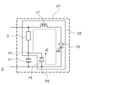
- FIG. 10C is a circuit diagram showing another example of the configuration of the load circuit section included in the electric pulse generator of the first embodiment, shown in accordance with FIG. 10B.
- FIG. 10C is a circuit diagram showing another example of the configuration of the load circuit section included in the electric pulse generator of the first embodiment, shown in accordance with FIG. 10B.
- FIG. 10C is a circuit diagram showing another example of the configuration of the load circuit section included in the electric pulse generator of the first embodiment, shown in accordance with FIG. 10B.
- FIG. 11 is a circuit block diagram showing a schematic diagram of an electric pulse generator according to a second embodiment.
- FIG. 11 is a circuit diagram showing the operation principle of an electric pulse generator according to a second embodiment.
- FIG. 11 is a circuit diagram showing the operation principle of an electric pulse generator according to a second embodiment.
- FIG. 12 is a graph showing an example of the behavior of a current flowing through an object to be energized after a switching element is turned on in an electric pulse generator of the second embodiment, in which the graph of FIG. 11 is also shown.
- FIG. 16C is a circuit diagram showing another example of the configuration of the load circuit section included in the electric pulse generator of the second embodiment, shown in accordance with FIG. 16B.
- FIG. 16C is a circuit diagram showing another example of the configuration of the load circuit section included in the electric pulse generator of the second embodiment, shown in accordance with FIG. 16B.
- FIG. 11 is a circuit block diagram illustrating an electric pulse generator according to a third embodiment.
- FIG. 11 is a circuit diagram showing the operation principle of an electric pulse generator according to a third embodiment.
- FIG. 11 is a circuit diagram showing the operation principle of an electric pulse generator according to a third embodiment.
- FIG. 21C is a circuit diagram showing another example of the configuration of the load circuit section included in the electric pulse generator of the third embodiment, shown following the example of FIG. 21B.
- FIG. 21C is a circuit diagram showing another example of the configuration of the load circuit section included in the electric pulse generator of the third embodiment, shown following the example of FIG. 21B.
- FIG. 21C is a circuit diagram showing another example of the configuration of the load circuit section included in the electric pulse generator of the third embodiment, shown following the example of FIG. 21B.
- FIG. 1 is a circuit block diagram showing a schematic diagram of a conventional electric pulse generator.
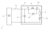
- FIG. 1 is a circuit block diagram showing a schematic configuration of an electric pulse generator according to the present embodiment.
- the electric pulse generator 1 includes a high voltage source 5 and a load circuit section 2.
- the high voltage source 5 is a voltage source capable of outputting a voltage on the order of kV.
- the electrical pulse generator 1 of this embodiment includes a switching element 6 that switches between electrical connection and disconnection between the high voltage source 5 and the load circuit section 2. Note that while FIG. 1 illustrates the switching element 6 as being provided outside the high voltage source 5, it may also be provided inside the high voltage source 5.
- the load circuit section 2 included in the electric pulse generator 1 of this embodiment includes a capacitor 11, a switching element 13, a diode 15, an inductor 17, and an object 3 to be energized.
- the object to be heated may be integrated with the object to be energized 3, or the object to be energized 3 and the object to be heated may be located apart from each other. This point will be described later.
- the capacitor 11 is arranged so that it can be charged based on the output voltage from the high voltage source 5 when the switching element 6 is turned on and the high voltage source 5 and the load circuit section 2 are electrically connected.
- the capacitor 11 is structured so that it can be charged with a voltage on the order of kV.
- the switching element 13 is connected in series with the current-carrying object 3.
- a series circuit (first closed circuit U1) is formed that includes the capacitor 11, the current-carrying object 3, the switching element 13, and the inductor 17.
- the switching element 13 is composed of a semiconductor element, and is typically a thyristor or an IGBT.
- the switching element 13 is a thyristor
- the switching element 13 is controlled to be turned on and off based on a gate signal.
- a signal voltage is applied between the gate terminal and the cathode terminal as a gate signal, the thyristor becomes conductive thereafter.
- connection point P1 has a cathode terminal connected to the first closed circuit U1 at connection point P1, and an anode terminal connected to the first closed circuit U1 at connection point P2.
- connection point P1 is electrically closer to the high potential side terminal of the capacitor 11 than connection point P2.
- FIG. 2 is a schematic diagram of an embodiment in which the object 3 to be energized is a flash lamp.
- the flash lamp 7 comprises an arc tube 23 made of quartz glass or the like, and a pair of electrodes (21, 22). A gas such as xenon is sealed inside the arc tube 23.
- the electric pulse generator 1 supplies an electric pulse to the flash lamp 7 as the object 3 to be energized, more specifically between the pair of electrodes (21, 22), causing the flash lamp 7 to emit light for a short period of time.
- a high energy of, for example, 5 kJ is supplied to the flash lamp 7.
- Light L7 from the flash lamp 7 is irradiated onto the object to be heated 30.
- This light L7 is absorbed by the surface region 31 of the object to be heated 30, thereby heating the surface region 31.
- the light L7 from the flash lamp 7 can be used to heat the surface of the organic layer as the object to be heated 30.
- a thin film of about 1 ⁇ m or less on the surface of the object to be heated 30 can be instantaneously heated to an extremely high temperature of about 800° C.
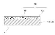
- the composite structure 4 shown in FIG. 3 includes a metal plate 41 as the current-carrying object 3, and constituent materials 43 and 45 as the heating object 30.
- the electric pulse is supplied to the metal plate 41 as the current-carrying object 3 by the electric pulse generator 1
- the current-carrying object 3 is heated by an electric energy defined by (current) 2 ⁇ (resistance value R of the metal plate 41), and this heat is transferred to the heating object 30.
- the heating object 30 and the current-carrying object 3 are peeled off.
- a part of the load circuit unit 2 is formed by the composite structure 4 in which the current-carrying object 3 and the heating object 30 are integrated.
- the method of transmitting energy to the heated object 30 is different, but the concept of transferring energy to a limited area is essentially the same as in the embodiment shown in FIG. 2.
- FIG. 4 is a cross-sectional view showing a composite structure of metal and insulating material as an example in which the current-carrying object 3 and the heating object 30 are integrated.
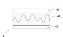
- the composite structure 4 when the composite structure 4 is a solar cell, as shown in FIG. 4, the composite structure 4 includes an upper metal electrode 47, an organic thin film layer 48, and a transparent electrode 49.
- the organic thin film layer 48 and the upper metal electrode 47 are peeled off. This allows the metal contained in the upper metal electrode 47 to be recovered and recycled.
- a part of the load circuit section 2 is formed by a composite structure 4 in which the object to be energized 3 and the object to be heated 30 are integrated.
- the composite structure 4 may be placed on the circuit while immersed in the conductive solution 55.
- the composite structure 4 cut to an appropriate size is immersed in the solution 55 while being contained in a container 56 with an opening on the periphery.
- An electric pulse is then supplied to the solution 55 via a pair of electrodes (51, 52).
- electricity flows through the metal plate 41 of the composite structure 4 via the conductive solution 55. This heats the interface between the metal plate 41 and the heating object 30 (constituent material 43 and constituent material 45) shown in FIG. 3.
- the composite structure 4 may be placed on the circuit while immersed in the conductive solution 55.
- the composite structure 4 cut to an appropriate size is immersed in the solution 55 while being contained in a container 56 with an opening on the periphery.
- An electric pulse is then supplied to the solution 55 via a pair of electrodes (51, 52).
- electricity flows through the metal plate 41 of the composite structure 4 via the conductive solution 55. This heats the interface between the metal plate 41 and the heating object 30 (cons
- the combined resistance component of the metal plate 41 and the conductive solution 55 corresponds to the current-carrying object 3.
- the solution 55 is also included in the heating object 30 as a result.
- the conductive solution 55 serves both as the current-carrying object 3 and the heating object 30, and constitutes part of the load circuit section 2.
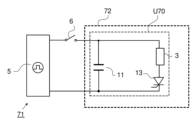
- FIG. 6 is a circuit block diagram showing a schematic configuration of an electric pulse generator 71 as a reference example, following the example of FIG. 1.
- the load circuit section 72 of the electric pulse generator 71 shown in FIG. 6 differs from the electric pulse generator 1 shown in FIG. 1 in that it does not include a diode 15 and an inductor 17. That is, in the load circuit section 72 shown in FIG. 6, when the switching element 13 is turned on, a series circuit (closed circuit U70) including the capacitor 11 and the object 3 to be energized is formed.
- the switching element 6 When starting the electric pulse generator 71, the switching element 6 is first made conductive to charge the capacitor 11 based on the output voltage from the high voltage source 5 (see FIG. 7A). At this time, the switching element 13 is made non-conductive so that there is no electrical continuity between the high voltage source 5 and the object 3 through which electricity is passed.
- the switching element 6 When charging of the capacitor 11 is completed, the switching element 6 is made non-conductive to disconnect the electrical connection between the high voltage source 5 and the load circuit section 72. Then, the switching element 13 is made conductive to allow the current resulting from the charging voltage of the capacitor 11 to flow through the current-carrying object 3 (see FIG. 7B).
- the high voltage source 5 is a voltage source capable of outputting a voltage on the order of kV
- the capacitor 11 is similarly configured to be capable of charging a voltage on the order of kV. Therefore, when the switching element 13 is in a conductive state, a high load current iZ resulting from a voltage on the order of kV instantaneously flows through the current-carrying object 3 via the switching element 13.
- the object 3 to be energized is a flash lamp 7
- current flows between a pair of electrodes (21, 22) while the gas sealed in the light-emitting tube 23 becomes plasma.
- the plasma-excited gas simultaneously emits light L7 of a specific wavelength.
- the light L7 emitted from the flash lamp 7 reaches the object 30 to be heated, and its surface region 31 is heated.
- the object 3 to be electrified when the object 3 to be electrified is a composite structure 4 made up of multiple stacked layers, the object 3 to be electrified heats itself due to the instantaneous flow of a high current, and this heat is transferred to the object to be heated 30.
- the high frequency of this current iZ also works to its advantage, and due to the skin effect, it may flow locally near the surface layer of the conductor contained in the object 3 to be electrified (metal plate 41 in the example of FIG. 3). In a short period of time, the temperature of the interface between the multiple layers that make up the composite structure 4 rises rapidly, causing the interface between the two to be locally heated and destroyed, and the two to be separated.
- the discharge current flowing from the capacitor 11 shown in Fig. 7B flows into the capacitor 11, and the capacitor 11 starts to charge with the reverse polarity.
- a reverse current iZ flows through the current-carrying object 3 due to the charging voltage of the capacitor 11 (see Fig. 7C).
- an oscillating current continues to flow through the current-carrying object 3 while reversing its polarity.
- the period of this oscillating current is determined by the capacitance component of the capacitor 11 and the parasitic inductance component present on the circuit in the closed circuit U70, as shown in the following formula. The period of oscillation is fixed.
- C Capacitance component
- L Inductance component
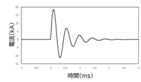
- Fig. 8 is an example of a graph showing the behavior of the current iZ flowing through the current-carrying object 3 and the voltage across the current-carrying object 3 after the switching element 13 is turned on after the capacitor 11 is completely charged by the output voltage from the high-voltage source 5 using the electric pulse generator 71 as the reference example shown in Fig. 6.
- a current flows through the current-carrying object 3 for a period of about several ms.
- the circuit conditions in Fig. 8 are as follows, and this is a reference example in which the current-carrying object 3 is a flash lamp.
- Inductance component (same as inductor 17 in FIG. 1): 12 ⁇ H Resistance value of current-carrying object 3: 50 m ⁇
- Capacitance of capacitor 11 400 ⁇ F Charging voltage of capacitor 11: 4000 V
- the time that current flows through the object 3 is at most a few milliseconds, which is much shorter than one second. For this reason, it would appear that the electric pulse generator 71 of the reference example also flows an instantaneous current through the object 3.
- the inventors of the present invention conceived that if the pulse width of the current could be narrowed even further than that of the electric pulse generator 71, the following would be possible.
- the light emission efficiency of the flash lamp 7 is increased by shortening the pulse width, while improving the control of heating of the surface region 31 of the object 30 to be heated.
- the controllability of the heating of the object 30 to be heated can be improved by using a short pulse width, thereby increasing the separation efficiency.
- the switching element 13 is a semiconductor element.
- the load circuit section 2 is provided with an inductor 17.
- the parasitic inductance present in the closed circuit without providing the inductor 17.
- the maximum allowable value for the current rise speed ( ⁇ I/ ⁇ t) may be specified as a rated value for a semiconductor switch that can be used as the switching element 13. If a current that is too steep flows through the semiconductor switch, the current may not be able to diffuse in time inside the semiconductor junction, causing the current to concentrate locally, which may result in the semiconductor switch being heated and destroyed. From this perspective, the maximum allowable value for the current rise speed may be set.
- the switching element 13 when charging of the capacitor 11 is completed, the switching element 13 is turned on to allow the current iZ derived from the charging voltage of the capacitor 11 to flow to the current-carrying object 3 (see FIG. 10A).
- the switching element 13 When the switching element 13 is turned on, the current iZ derived from a voltage on the order of kV instantaneously flows through the current-carrying object 3 via the switching element 13.
- the load circuit section 2 of the electric pulse generator 1 includes the diode 15.
- the connection point P1 of the cathode terminal of the diode 15 is electrically closer to the high potential terminal of the capacitor 11 than the connection point P2 of the anode terminal. Therefore, the current iZ that has flowed through the current-carrying object 3 bypasses the capacitor 11 and flows through the diode 15 (see FIG. 10B). In other words, after the capacitor 11 is discharged, the diode 15, inductor 17, and current-carrying object 3 are connected in series to form a second closed circuit U2 that does not include the capacitor 11.
- the electric pulse generator 1 of this embodiment does not cause the capacitor 11 to be charged again with the opposite polarity, so the time during which the current iZ flows through the object 3 to be energized is significantly shortened.
- FIG. 11 is an example of a graph showing the behavior of the current iZ flowing through the current passing object 3 and the voltage across the current passing object 3 after the switching element 13 is turned on after the capacitor 11 has been completely charged by the output voltage from the high voltage source 5 using the electric pulse generator 1 of this embodiment.
- FIG. 11 also shows a graph showing the behavior of the current iZ in the electric pulse generator 71 of the reference example shown in FIG. 8. Comparing the waveforms of both, it can be seen that the time ( ⁇ 1) during which the current iZ flows through the current passing object 3 with the electric pulse generator 1 of this embodiment can be shortened compared to the time ( ⁇ 0) during which the current iZ flows when there is no diode 15 (reference example).
- the circuit conditions in Fig. 11 are as follows: That is, the circuit conditions in Fig. 11 are the same as those in Fig. 8 except for the presence of the diode 15.
- the following values are a reference example when the object 3 to be energized is a flash lamp.
- Inductance component (same as inductor 17 in FIG. 1): 12 ⁇ H Resistance value of current-carrying object 3: 50 m ⁇
- the current iZ flowing through the current passing object 3 may include a ringing current that is less than 10% of the current value of the peak current that flows after the peak current.
- This ringing current is related to a certain parasitic inductance in the circuit.
- the period ( ⁇ 1) of the main pulse width which is the time width until the current waveform begins to essentially taper off, is a short time of approximately 1.2 ms.
- a ringing current that is less than 10% of the current value of the peak current may still be observed, but this level is considered to have no significant effect on heating.
- FIGS. 12 to 14 are circuit diagrams that show, in a schematic manner similar to FIG. 10B, other configuration examples of the load circuit section 2 included in the electric pulse generator 1 of this embodiment. That is, FIGS. 12 to 14 all show the behavior of the current iZ after the discharge of the capacitor 11 is completed.
- first closed circuit U1 a series circuit that includes the capacitor 11, the current-carrying object 3, the switching element 13, and the inductor 17. Then, when the switching element 13 transitions from a non-conducting state to a conducting state while the capacitor 11 is in a charged state, the current iZ that flowed through the current-carrying object 3 bypasses the capacitor 11 and flows through the diode 15. After the capacitor 11 is discharged, the diode 15, the inductor 17, and the current-carrying object 3 are connected in series to form a second closed circuit U2 that does not include the capacitor 11.
- the electric pulse generator 1 of this embodiment produces short pulses, which reduces damage to the object 3 to be energized and the object 30 to be heated, and can efficiently heat the object 30 to be heated in an appropriate range with good reproducibility.
- FIG. 15 is a circuit block diagram showing the configuration of the electric pulse generator 1 of this embodiment, following the same pattern as FIG. 1.
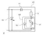
- the electric pulse generator 1 of this embodiment differs from the first embodiment in the configuration of the load circuit section 2. Specifically, it differs in that the diode 15 is connected in parallel to the series circuit of the current-carrying object 3 and the capacitor 11.
- Figures 16A and 16B are similar to Figures 10A and 10B, in that only the load circuit section 2 of the electrical pulse generator 1 of this embodiment is extracted.
- the switching element 13 When charging of the capacitor 11 is completed, the switching element 13 is turned on to allow the current iZ derived from the charging voltage of the capacitor 11 to flow to the current-carrying object 3 (see FIG. 16A). When the switching element 13 is turned on, the current iZ derived from a voltage on the order of kV instantaneously flows through the current-carrying object 3 via the switching element 13.
- the load circuit section 2 of the electric pulse generator 1 of this embodiment also includes a diode 15, as in the first embodiment.
- the connection point P1 of the cathode terminal of the diode 15 is electrically closer to the high potential terminal of the capacitor 11 than the connection point P2 of the anode terminal. Therefore, the current iZ that has flowed through the current-carrying object 3 bypasses the capacitor 11 and the current-carrying object 3 and flows through the diode 15 (see FIG. 16B).
- the diode 15 and the inductor 17 are connected in series, and a second closed circuit U2 is formed that does not include the capacitor 11 and the current-carrying object 3.
- the capacitor 11 does not charge with reverse polarity, so the time during which the current iZ flows through the object 3 is significantly shortened. Furthermore, compared to the first embodiment, the time during which the current iZ flows through the object 3 can be further shortened.
- the capacitor 11 is charged via the current-carrying object 3.
- the current-carrying object 3 is a flash lamp 7
- the flash lamp 7 exhibits insulating properties until it starts to light up, and so the current-carrying object 3 is essentially insulating during this period. In this case, the capacitor 11 cannot be charged via the current-carrying object 3.
- a resistor of about several ohms may be connected in parallel to the current-carrying object 3 (here, the flash lamp 7). Also, a diode may be added to ensure the charging path.
- FIG. 17 is an example of a graph showing the behavior of the current iZ flowing through the current-carrying object 3 after the switching element 13 is turned on after the capacitor 11 has been completely charged by the output voltage from the high voltage source 5 using the electric pulse generator 1 of this embodiment.
- FIG. 17 also shows a graph showing the behavior of the current iZ in the electric pulse generator 71 of the first embodiment shown in FIG. 11.
- the time period during which the current iZ flows through the object 3 to be energized is further shortened compared to the first embodiment.
- the period ( ⁇ 1) of the main pulse width which is the time width from the timing at which the peak current is generated to the timing at which the current starts to taper off, was approximately 1.2 ms, whereas in the case of this embodiment, the period ( ⁇ 2) is approximately 0.2 ms.
- the period of the pulse width can be significantly shortened compared to the electric pulse generator 71 of the reference example.
- the electric pulse generator 1 of this embodiment is characterized in that the diode 15 is arranged in parallel to the connection circuit between the capacitor 11 and the current-carrying object 3, as shown in FIG. 15.
- the capacitor 11, the current-carrying object 3, and the diode 15 are arranged as close as possible to each other, the occurrence of a current derived from a parasitic inductance other than the inductor 17 on the circuit in the second closed circuit U2 is suppressed.
- the electric pulse generator 1 of this embodiment as shown in FIG. 17, almost no ringing current flows after the main pulse is generated.
- FIGS. 18-19 are circuit diagrams showing another example of the configuration of the load circuit section 2 included in the electric pulse generator 1 of this embodiment, following the example of FIG. 16B. That is, FIGS. 18-19 all show the behavior of the current iZ after the discharge of the capacitor 11 is complete.
- first closed circuit U1 a series circuit that includes the capacitor 11, the current-carrying object 3, the switching element 13, and the inductor 17. Then, when the switching element 13 transitions from a non-conducting state to a conducting state while the capacitor 11 is in a charged state, the current iZ that flowed through the current-carrying object 3 bypasses the capacitor 11 and the current-carrying object 3 and flows through the diode 15. After the capacitor 11 is discharged, the diode 15 and the inductor 17 are connected in series to form a second closed circuit U2 that does not include the capacitor 11 or the current-carrying object 3.
- the electric pulse generator 1 of this embodiment produces an electric pulse with a shorter pulse width period than the first embodiment, so that the object to be heated 30 can be heated efficiently and reproducibly within an appropriate range while reducing damage to the object to be energized 3 and the object to be heated 30.
- FIG. 20 is a circuit block diagram showing the configuration of the electric pulse generator 1 of this embodiment, following the same pattern as FIG. 1.
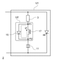
- the electric pulse generator 1 of this embodiment differs from the first embodiment in the configuration of the load circuit section 2. Specifically, it differs in that the diode 15 is connected in parallel to the inductor 17.
- Figures 21A and 21B are similar to Figures 10A and 10B, in that only the load circuit section 2 of the electrical pulse generator 1 of this embodiment is extracted.
- the switching element 13 When charging of the capacitor 11 is completed, the switching element 13 is turned on to allow the current iZ derived from the charging voltage of the capacitor 11 to flow to the current-carrying object 3 (see FIG. 21A). When the switching element 13 is turned on, the current iZ derived from a voltage on the order of kV instantaneously flows through the current-carrying object 3 via the switching element 13.
- the load circuit section 2 of the electric pulse generator 1 of this embodiment also includes a diode 15, as in the first embodiment.
- the connection point P1 of the cathode terminal of the diode 15 is electrically closer to the high potential terminal of the capacitor 11 than the connection point P2 of the anode terminal.
- the current iZ from the capacitor 11 flows to the current-carrying object 3 via the inductor 17, not via the diode 15.
- the current iZ flows from the connection point P2 to the connection point P1 via the diode 15 (see FIG. 21B).
- the current iZ flows instantaneously toward the current-carrying object 3, the current no longer flows toward the current-carrying object 3, but flows through the second closed circuit U2 formed by the inductor 17 and the diode 15.
- the diode 15 and the inductor 17 are connected in series to form a second closed circuit U2 that does not include the capacitor 11 or the current-carrying object 3.
- the time during which the current iZ flows through the object 3 can be further shortened in the electric pulse generator 1 of this embodiment than in the first embodiment.
- a current originating from the parasitic inductance in the first closed circuit U1 flows through the current-carrying object 3, and as a result, the ringing current may continue to flow while attenuating by about 10% or less. In this case, the current flowing through the current-carrying object 3 does not actually become zero.
- the electric pulse generator 1 of the first embodiment described above with reference to FIG. 1, etc. the current path flowing through the current-carrying object 3 is bypassed by the diode 15, so that the current flowing through the current-carrying object 3 can be made almost zero.
- FIGS. 22 to 24 are circuit diagrams showing, in a schematic manner following FIG. 21B, another example of the configuration of the load circuit section 2 included in the electric pulse generator 1 of this embodiment. That is, FIGS. 22 to 24 all show the behavior of the current iZ after the discharge of the capacitor 11 is completed.
- a series circuit (first closed circuit U1) is formed that includes the capacitor 11, the current-carrying object 3, the switching element 13, and the inductor 17. Then, when the switching element 13 transitions from a non-conducting state to a conducting state while the capacitor 11 is in a charged state, the current iZ flows instantaneously through the current-carrying object 3, and then the induced current of the inductor 17 flows through the second closed circuit U2, which is formed by connecting the diode 15 and the inductor 17 in series and does not include the capacitor 11 or the current-carrying object 3.
- the electric pulse generator 1 of this embodiment produces short pulses, which reduces damage to the object 3 to be energized and the object 30 to be heated, and can efficiently heat the object 30 to be heated in an appropriate range with good reproducibility.
- the electrical pulse generator 1 of each embodiment can reduce the variation and fluctuation of the output energy while shortening the period during which the electrical pulse is provided.
- Electric pulse generator 2 Load circuit section 3: Electrically conductive object 4: Composite structure 5: High voltage source 6: Switching element 7: Flash lamp 11: Capacitor 13: Switching element 15: Diode 17: Inductor 23: Arc tube 30: Heating object 31: Surface area of heating object 32: Lower layer 33: Screw member 41: Metal plate 41a, 41b: Part derived from metal plate 43: Constituent material 45: Constituent material 47: Upper metal electrode 48: Organic thin film layer 49: Transparent electrode layer 51: Electrode 52: Electrode 55: Conductive solution 56: Storage container 71: Reference example electric pulse generator 72: Load circuit section 90: Electrically conductive object 91: Capacitor 92: Mechanical switch 95: High voltage source 96: Switching element 100: Conventional example electric pulse generator L7: Light P1 : Connection point P2 : Connection point U1 : First closed circuit U2 : Second closed circuit iZ : Current ⁇ 0 to ⁇ 3: Period
Landscapes
- Generation Of Surge Voltage And Current (AREA)
- Control Of Resistance Heating (AREA)
- Circuit Arrangement For Electric Light Sources In General (AREA)
Abstract
短時間で高い電流ピークを示すパルス電流を、高い再現性の下で発生させることのできる装置を提供する。 電気パルス発生装置は、高電圧源からの出力電圧を印加可能に配置された負荷回路部を備える。負荷回路部は、通電対象物に対して直列に接続されたスイッチング素子と、コンデンサと、ダイオードとを有し、スイッチング素子が導通状態の下で、コンデンサと通電対象物とスイッチング素子とを含む直列回路である第一閉回路を形成する。ダイオードは、アノード端子及びカソード端子が、それぞれ第一閉回路上の2箇所に接続されている。コンデンサが充電された状態の下でスイッチング素子を非導通状態から導通状態に遷移させた時点において、カソード端子と第一閉回路との接続点が、アノード端子と第一閉回路との接続点よりも、コンデンサの高電位側の端子に電気的に近い位置に配置されている。
Description
本発明は、対象物に対して電気パルスを印加する、電気パルス発生装置に関する。
従来、フラッシュランプを点灯させるための手段として、パルス発生回路が利用されている(例えば、特許文献1参照)。
フラッシュランプは、主に、可視域から赤外域にわたる光を発し、この光を対象物に照射することで対象物を加熱する、加熱用光源として利用されるランプである。このランプに対して電流が供給されると、ランプからは供給された電流の波形に従った光量が得られる。よって、この電流波形、特にパルス幅を制御することにより、対象物への加熱深度を制御することができる。例えば、電流波形のパルス幅とピーク値を適切に制御することにより、対象物への熱的なダメージを抑制しつつ、対象物の表層のみを加熱することが可能である。
上記の技術は、半導体製造プロセスにおいて、基板への加熱に適用することができる。
基板は、下地ウェハの上層に、複数の半導体層や絶縁層が積層される。例えば、半導体層の形成に際しては、ドーピングした不純物を拡散させるためにアニール処理が行われる。
このアニール処理の際に、フラッシュランプが利用される。フラッシュランプに対して供給される電流の波形を適切に制御することにより、基板の内部には損傷を生じさせずに、基板の表層に形成されている半導体層のみを選択的に加熱することができる。
基板は、下地ウェハの上層に、複数の半導体層や絶縁層が積層される。例えば、半導体層の形成に際しては、ドーピングした不純物を拡散させるためにアニール処理が行われる。
このアニール処理の際に、フラッシュランプが利用される。フラッシュランプに対して供給される電流の波形を適切に制御することにより、基板の内部には損傷を生じさせずに、基板の表層に形成されている半導体層のみを選択的に加熱することができる。
近年、半導体製品の微細化、高集積化が進展している。半導体製品を高集積化する観点から、多数の薄膜が積層される。このため、フラッシュランプの役割として、その薄膜のみを加熱制御するような技術が、益々求められている。なぜなら、仮に、表層以外の箇所に対しても加熱されてしまうと、その後に層の形成と加熱処理を繰り返すことで、表層よりも深い位置に形成されている層に対して複数回加熱されることになり、半導体の品質に影響が生じる懸念があるためである。かかる観点から、加熱対象物に対して極めて浅い表面のみを加熱制御する方法として、フラッシュランプからの光の照射パルス幅を小さくする方法が知られている。
対象物の表面近傍に対して選択的に加熱する技術は、層状の部材をリサイクルする際にも適用することができる。
使われなくなった通信端末機器や家電機器等の電気製品には、利用可能な資源が含まれている場合がある。省資源の観点から、使われなくなった前記電気製品は、業者によって回収された後、分解・解体してリサイクルすることが求められている。従来、この種の作業は人手による分解、又は破砕機などで物理的に解体されることが多い。しかし、そのような作業では人手を多く要する上、解体後の部材の品質が低いことでリサイクルできる割合が低くなる傾向があった。
リサイクル対象となる廃棄物としては、金属などの導電性物質に対して、絶縁物質や半導体が積層されてなるものがある。より詳細な例としては、金属製の材料に有機物材料が塗布されてなる複合材、金属製の材料に塗料が施されてなる複合材、金属製の材料に絶縁性の材料が貼り付けられ又は蒸着されてなる複合材、等が挙げられる。
上記のように、金属製の材料を含む複合材からなる廃棄物は、粉砕後に燃焼し、得られた燃焼灰から必要な金属を分別して抽出することで、リサイクルに資する。しかし、この方法は、金属が金属化合物や合金に変性している場合があり、その後の処理が必要になる上、燃焼時にCO2排出量が多くなり、環境負荷的に問題がある。湿式法による場合には、取り出された材料は電気分解やイオン交換や化学反応などの化学処理がなされるが、初めから、純度の高い材料を分離回収していないためエネルギー的な負担が大きい。
上記の観点から、特定の対象物を加熱するために間接的にランプを利用するものであって、そのランプに対して点灯パルス幅を短縮化し選択的に加熱する方法が提案されている(下記特許文献1)。また、別の事例として、間接的にランプを利用するのではなく、リサイクル対象物に対して直接パルス電圧を印加して選択的に加熱して解体する方法が提案されている(下記特許文献2)。
特許文献1には、ランプに投入されるエネルギーを小さくし、電源を小さくするなどの目的で、フラッシュランプの点灯パルス幅の短縮化が進められていることが記載されている。また、半導体のアニール用途以外にも、セラミック薄膜表面の改質や光硬化による光学部品の接着固定などといった分野で短パルス光が求められていることが記載されている。
しかしながら、特許文献1には短パルス化についての詳細な言及はされていない。対象物に対する短時間の光照射、言い換えれば短時間のエネルギー供給は、対象物に加熱履歴を生じさせないためにも重要であると考えられる。短時間のエネルギー供給により、対象物(エネルギー被供給側)の表面のみを選択的に昇温することが可能となる。一方で、対象物に対する表面処理等の目的を奏するためには、十分なエネルギー量を供給する必要がある。短時間で目的の処理を実現するためには、単位時間あたりのエネルギーを高める必要があり、対象物への過剰な加熱やランプへのダメージに繋がる可能性がある。
特許文献2に記載された技術は、電池を構成する正極金属箔を通電対象物として、この通電対象物にパルス電流を適切に流すことにより、正極金属箔とその箔表面に接合した活物質とを箔から分離するというものである。つまり、特許文献2に記載された技術においては、通電対象物に対して高いピーク電流を供給することで、加熱対象物であるバインダーへの投入エネルギーを制御することが重要である。これは前述のランプによる加熱から全く同じ発想である。しかしながら、短時間で高いパルス電流を、再現よく発生させることのできる電源装置を実現するには、技術的な難易度がある。短時間で高いパルス電流を、再現よく発生させることのできる電源装置については、特許文献1及び2には開示されていない。
本発明は、上記の課題に鑑み、加熱対象物の表面近傍を選択的に加熱すべく、短時間で高い電流ピークを示すパルス電流を、高い再現性の下で発生させることのできる、電気パルス発生装置を提供することを目的とする。
本発明に係る電気パルス発生装置は、通電対象物に対して電気パルスを印加する装置であって、
高電圧源と、前記高電圧源からの出力電圧を印加可能に配置された負荷回路部とを備え、
前記負荷回路部は、
前記通電対象物と、
前記通電対象物に対して直列に接続されたスイッチング素子と、
前記高電圧源と前記負荷回路部とが電気的に接続されると前記高電圧源からの出力電圧に基づいて充電可能な位置に配置されたコンデンサと、
アノード端子及びカソード端子を含むダイオードとを有し、
前記負荷回路部は、前記スイッチング素子が導通状態の下で、前記コンデンサと、前記通電対象物と、前記スイッチング素子とを含む直列回路である第一閉回路を形成し、
前記ダイオードは、前記アノード端子及び前記カソード端子が、それぞれ前記第一閉回路上の2箇所に接続されており、
前記コンデンサが充電された状態の下で前記スイッチング素子を非導通状態から導通状態に遷移させた時点において、前記カソード端子と前記第一閉回路との接続点が、前記アノード端子と前記第一閉回路との接続点よりも、前記コンデンサの高電位側の端子に電気的に近い位置に配置されていることを特徴とする。
高電圧源と、前記高電圧源からの出力電圧を印加可能に配置された負荷回路部とを備え、
前記負荷回路部は、
前記通電対象物と、
前記通電対象物に対して直列に接続されたスイッチング素子と、
前記高電圧源と前記負荷回路部とが電気的に接続されると前記高電圧源からの出力電圧に基づいて充電可能な位置に配置されたコンデンサと、
アノード端子及びカソード端子を含むダイオードとを有し、
前記負荷回路部は、前記スイッチング素子が導通状態の下で、前記コンデンサと、前記通電対象物と、前記スイッチング素子とを含む直列回路である第一閉回路を形成し、
前記ダイオードは、前記アノード端子及び前記カソード端子が、それぞれ前記第一閉回路上の2箇所に接続されており、
前記コンデンサが充電された状態の下で前記スイッチング素子を非導通状態から導通状態に遷移させた時点において、前記カソード端子と前記第一閉回路との接続点が、前記アノード端子と前記第一閉回路との接続点よりも、前記コンデンサの高電位側の端子に電気的に近い位置に配置されていることを特徴とする。
負荷回路部には、コンデンサ、スイッチング素子、及びダイオードが備えられている。
スイッチング素子は、通電対象物と直列に接続されており、コンデンサは高電圧源からの電圧に基づいて充電可能な位置に配置されている。負荷回路部は、スイッチング素子が導通状態の下で、コンデンサと、通電対象物と、スイッチング素子とを含む直列回路(第一閉回路)を形成する。
スイッチング素子は、通電対象物と直列に接続されており、コンデンサは高電圧源からの電圧に基づいて充電可能な位置に配置されている。負荷回路部は、スイッチング素子が導通状態の下で、コンデンサと、通電対象物と、スイッチング素子とを含む直列回路(第一閉回路)を形成する。
スイッチング素子を非導通状態として、高電圧源と負荷回路部とを接続することで、高電圧源からの電圧に由来してコンデンサが充電される。その後、高電圧源と負荷回路部との電気的接続を解除した状態で、スイッチング素子を導通することで、コンデンサの充電電圧に由来した高電流が、スイッチング素子を介して通電対象物に対して供給される。スイッチング素子が導通される直後に電流が流れるため、この電流はパルス状を示す。
更に、前述したように、負荷回路部にはダイオードが備えられている。このダイオードは、コンデンサが充電された状態の下でスイッチング素子を非導通状態から導通状態に遷移させた時点において、カソード端子と第一閉回路との接続点が、アノード端子と第一閉回路との接続点よりも、コンデンサの高電位側の端子に電気的に近い位置に配置されている。つまり、コンデンサが充電された状態の下で、通電対象物に対して高電流を流すべくスイッチング素子を導通状態にすると、コンデンサの充電電圧に由来した電流が通電対象物に流れた後は、コンデンサを迂回し、ダイオードを介して電流が流れる。この結果、コンデンサは、スイッチング素子が導通された後は、スイッチング素子が導通される直前におけるコンデンサの充電状態から、逆極性の充電状態に移行することがない。つまり、第一閉回路内において、極性が変化する振動電流が流れることが抑制される。このことは、通電対象物に対して電流が供給される時間を短縮化できること、言い換えれば、通電対象物に流れる電流のパルス幅を短くできることを意味する。
具体的な一例として、ダイオードを備えていない場合には、例えば、数ms程度の時間にわたる交流電流(AC)となる減衰振動の電流波形であったものが、ダイオードを付加することで、単パルスとなり、しかも電流供給の全体期間も低減することができる。
上記電気パルス発生装置は、一例としてフラッシュランプに適用することが可能である。本発明に係る電気パルス発生装置を用いてフラッシュランプにパルス電流を供給することの効果について、従来の電気パルス発生装置を用いた場合と比較して説明する。
図25は、フラッシュランプを点灯する際に利用される、従来の電気パルス発生装置の構成を模式的に示す回路図である。図25に示すように、従来の電気パルス発生装置100は、高電圧源95と、高電圧源95から発生された電圧が印加される負荷回路部とを備える。より詳細には、この負荷回路部は、コンデンサ91と、メカニカルスイッチ92と、通電対象物90とを含む閉回路U100で形成されている。この例では、通電対象物90がフラッシュランプに対応する。メカニカルスイッチ92は、機械的な接触によって通電/非通電を切り替えるスイッチであるが、ギャップスイッチであってもよい。
なお、図25に示すスイッチング素子96は、高電圧源95とコンデンサ91との接続状態を切り替える目的で設けられている。スイッチング素子96が導通されると、高電圧源95から出力される電圧によってコンデンサ91が充電を開始する。コンデンサ91の充電が完了すると、スイッチング素子96をOFFにし、メカニカルスイッチ92をONにすることで、コンデンサ91の充電電圧に由来した高電流が通電対象物90に供給される。
ただし、図25に示す電気パルス発生装置100の場合、実際には通電対象物90に対して、数十ms~100ms程度の時間にわたって交流電流(減衰振動電流)が流れる。
この点については、「発明を実施するための形態」の項において、図8を参照して後述される。
この点については、「発明を実施するための形態」の項において、図8を参照して後述される。
つまり、図25に示す電気パルス発生装置100を用いて通電対象物90に対してパルス電流を供給した場合、実際には通電対象物90に対して減衰振動波形を示す電流が供給される。このことは、通電対象物90がフラッシュランプである場合、フラッシュランプから加熱対象物に対して、ある程度の長さ(上記数十ms~100ms)にわたって加熱光(加熱対象物の吸収波長の光)が照射されることを意味する。この結果、加熱対象物の表層のみならず、深さ方向にも熱エネルギーが供給されてしまう。加熱対象物が半導体層を含むウェハである場合には、最表面以外の層も加熱されてしまい、半導体の品質に影響が生じる懸念がある。
更に、通電対象物90がフラッシュランプの場合、高い電流を流し過ぎるとランプに対してダメージを与える可能性がある。フラッシュランプを用いて加熱対象物の表層付近を選択的に加熱するためには、ランプに対して短期間に高いピーク値の電流を供給してランプを放電させて、短い期間において発光させればよい。このためには、例えばkVオーダーの高い電圧を発生させ、それを放電することのできる高電圧源を単に準備すればよいようにも思える。しかしながら、通電対象物であるランプに高い電流を提供することで、加熱対象物に対して照射される輝度が高くなり過ぎてしまい、加熱対象物の薄膜の過剰な加熱による破壊又は蒸発が起きてしまう課題がある。
次に、通電対象物に対してパルス電流を供給することで、導電物質としての通電対象物と他の部材とが接触して一体化されてなる複合部材から、通電対象物と他の部材とを分離する場合について説明する。例えば、薄膜状の導電体である第一部材を、第一部材よりも導電性の低い材料からなる第二部材から分離・解体するためには、第一部材と第二部材の界面付近にできるだけ高い電流を流して当該領域を瞬時的に高温にし、第一部材と第二部材の間の接着力を低下させることが必要となる。第一部材に対して期間の短い電流(短パルス電流)を流すことで、導電体が溶ける前に、第二部材との接合部の浅い表層部分の温度を上げて、第二部材の中でも特に第一部材に近い領域の接着剤を溶融することができる。また、副次的には、電流の周波数を高めることにより、電流が導体の表面を選択的に流れる表皮効果も利用できる。高周波電流を利用することで、第一部材の表面近傍、言い換えれば、第一部材と第二部材との界面近傍に集中的に高電流を流し、当該領域を瞬時的に高温にすることが可能となる。このような観点から、通電対象物に対してはパルス状の電流を供給することが好ましい。
第一部材の構成材料としては、例えば、銅、アルミニウム、鉄、ニッケル、又はそれらの合金からなる導電物質が挙げられる。また、第二部材の構成材料としては、樹脂や塗料などの有機物、酸化物金属、又はそれらの混合物である絶縁物質や半導体が挙げられる。
つまり、第一部材と第二部材の間の接着力を低下させるためには、第一部材と第二部材の界面近傍に、高周波で高い電流を流すことが必要となる。この点のみを考えれば、例えばkVオーダーの高い電圧を発生させることのできる高電圧源を単に準備すれば良いようにも思える。
しかしながら、通電対象物に対して印加される電圧が高すぎた場合、薄膜状の通電対象物の導電部が過剰に加熱され、破壊又は蒸発することがある。この理由としては、通電対象物に対して供給されるエネルギーが高すぎたことによるものと考えられ、この場合は第一部材と第二部材とを分離できたとは言えなくなる。
上記において、電気パルス発生装置を、フラッシュランプの点灯回路に利用する場合と、層状の複合部材の加熱に利用する場合の双方において、生じ得る課題について説明した。投入エネルギーは、電力を時間で積分した値で規定される。本発明に係る電気パルス発生装置によれば、加熱対象物に対してエネルギーが供給される時間を短く適切な値に設定できるため、加熱対象範囲を限定したエネルギーを供給することができるとともに、加熱対象部と通電対象物の両方に対するダメージを抑制することができる。
なお、前記負荷回路部を構成する前記スイッチング素子は、半導体素子からなるものとしても構わない。
上述したように、コンデンサに充電された高電圧に由来する電流を通電対象物に流すべくスイッチング素子を導通すると、当該スイッチング素子には瞬時的に高い電流が流れる。スイッチング素子が機械的な素子である場合には、スイッチング素子の接点が消耗し、経時的にスイッチング素子の内部抵抗が変化したり、場合によっては開閉制御が不能になることが起こり得る。このため、異なる通電対象物を継続して解体する場合、経時的に解体の精度が低下する可能性がある。
これに対し、上記のように前記スイッチング素子を半導体素子で構成することで、経時的な劣化や摩耗が抑制される。
半導体素子としては、典型的には、高い電圧耐性を示すサイリスタ、高電圧IGBT等が利用可能である。
前記高電圧源と前記負荷回路部とが電気的に接続されたときに前記通電対象物に流れる負荷電流は、ピーク電流と、前記ピーク電流の後に流れる前記ピーク電流の電流値の10%未満のリンギング電流とを含み、
前記負荷電流は、前記ピーク電流の発生タイミングから前記リンギング電流の発生タイミング迄の間において、極性を変化させることなく実質的に逓減するものとしても構わない。
前記負荷電流は、前記ピーク電流の発生タイミングから前記リンギング電流の発生タイミング迄の間において、極性を変化させることなく実質的に逓減するものとしても構わない。
好ましくは、前記負荷電流は、前記ピーク電流の発生タイミングから前記リンギング電流の発生タイミング迄の時間幅である主パルス幅が1.2ms以下である。この構成によれば、通電対象物に対して電流が供給される時間が極めて短時間になる。
前記負荷回路部はインダクタを含み、
前記第一閉回路は、前記コンデンサと、前記通電対象物と、前記スイッチング素子と、前記インダクタとを含む直列回路であるものとしても構わない。
前記第一閉回路は、前記コンデンサと、前記通電対象物と、前記スイッチング素子と、前記インダクタとを含む直列回路であるものとしても構わない。
前記負荷回路部は、前記コンデンサの放電後に、直列に接続された前記ダイオードと前記インダクタと前記通電対象物とを含み、且つ前記コンデンサを含まない、第二閉回路を形成するものとしても構わない。
前記負荷回路部は、前記コンデンサの放電後に、直列に接続された前記ダイオードと前記インダクタとを含み、且つ前記コンデンサ及び前記通電対象物を含まない、第二閉回路を形成するものとしても構わない。
本発明の解体装置によれば、対象物に含まれる資源の回収率を高く維持するために必要な高電圧源の印加電圧の範囲を従来よりも拡げることができる。
本発明の電気パルス発生装置の各実施形態につき、適宜図面を参照して説明する。なお、以下の各図面は模式的に示したものである。また、各図面に図示された回路は一例であり、本発明の範囲は、図示された回路と等価的な回路を包含する。
[第一実施形態]
図1は、本実施形態の電気パルス発生装置の構成を模式的に示す回路ブロック図である。図1に示すように、電気パルス発生装置1は、高電圧源5と負荷回路部2とを備える。
高電圧源5は、kVオーダーの電圧を出力可能な電圧源である。
図1は、本実施形態の電気パルス発生装置の構成を模式的に示す回路ブロック図である。図1に示すように、電気パルス発生装置1は、高電圧源5と負荷回路部2とを備える。
高電圧源5は、kVオーダーの電圧を出力可能な電圧源である。
本実施形態の電気パルス発生装置1は、高電圧源5と負荷回路部2との電気的な接続/非接続を切り替えるスイッチング素子6を備える。なお、図1には、スイッチング素子6が高電圧源5の外部に設けられているように図示されているが、高電圧源5の内部に設けられていても構わない。
本実施形態の電気パルス発生装置1が備える負荷回路部2は、コンデンサ11と、スイッチング素子13と、ダイオード15と、インダクタ17と、通電対象物3とを備える。
なお、電気パルス発生装置1が対象物(加熱対象物)の加熱に利用される際、加熱対象物が通電対象物3と一体化されていても構わないし、通電対象物3と加熱対象物が離れた場所に設置されていても構わない。この点については後述される。
なお、電気パルス発生装置1が対象物(加熱対象物)の加熱に利用される際、加熱対象物が通電対象物3と一体化されていても構わないし、通電対象物3と加熱対象物が離れた場所に設置されていても構わない。この点については後述される。
コンデンサ11は、スイッチング素子6が導通されることで、高電圧源5と負荷回路部2とが電気的に接続されると高電圧源5からの出力電圧に基づいて充電可能に配置されている。コンデンサ11は、kVオーダーの電圧を充電可能な構造である。
スイッチング素子13は、通電対象物3と直列に接続されている。スイッチング素子13が導通されると、コンデンサ11と、通電対象物3と、スイッチング素子13と、インダクタ17とを含む直列回路(第一閉回路U1)が形成される。スイッチング素子13は、半導体素子で構成されており、典型的にはサイリスタやIGBTである。
スイッチング素子13がサイリスタである場合、スイッチング素子13は、ゲート信号に基づいてON/OFF制御される。詳細には、ゲート端子‐カソード端子の間にゲート信号としての信号電圧が一旦印加されると、以降はサイリスタが導通状態となる。
ダイオード15は、カソード端子が接続点P1において第一閉回路U1と接続され、アノード端子が接続点P2において第一閉回路U1と接続されている。ここで、接続点P1と接続点P2の関係は以下の通りである。コンデンサ11が充電された状態の下で、スイッチング素子13を非導通状態から導通状態に遷移すると、接続点P1は接続点P2よりもコンデンサ11の高電位側の端子に電気的に近い位置である
図2は、通電対象物3をフラッシュランプとした場合の実施形態を模式的に示す図面である。図2に示すように、フラッシュランプ7は、石英ガラス等からなる発光管23と、一対の電極(21,22)とを備えている。発光管23の内部にはキセノン等のガスが封入されている。電気パルス発生装置1によって、通電対象物3としてのフラッシュランプ7に対して、より詳細には一対の電極(21,22)の間に電気パルスが供給されることで、フラッシュランプ7が短時間発光する。フラッシュランプ7には、例えば、5kJもの高いエネルギーが供給される。
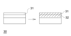
フラッシュランプ7からの光L7は、加熱対象物30に照射される。この光L7は、加熱対象物30の表面領域31で吸収されることで、表面領域31を加熱する。例えば、積層化された有機物から構成される太陽電池の製造プロセスにおいて、フラッシュランプ7からの光L7を利用して、加熱対象物30としての有機物層の表面を加熱することができる。具体的には、加熱対象物30の表面の約1μm以下という薄膜に対して、800℃程度の極めて高い温度に、瞬間的に加熱できる。電気パルス発生装置1からフラッシュランプ7に対して供給される電気パルスに関して、パルス幅と電流値を適切に制御することで、加熱対象物30の表面領域31のみを選択的に加熱することが可能となる。
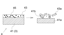
図3は、通電対象物3と加熱対象物30とが一体化されている例としての、金属と絶縁物質との複合構造物を模式的に示す断面図の一例である。図3に示す複合構造物4は、通電対象物3としての金属板41と、加熱対象物30としての構成材料43及び構成材料45を含む。電気パルス発生装置1によって、通電対象物3としての金属板41に対して電気パルスが供給されると、通電対象物3が、(電流)2×(金属板41の抵抗値R)によって規定される電気的エネルギーにより加熱されると共に、この熱が加熱対象物30に伝達される。この結果、加熱対象物30と通電対象物3が剥離される。この形態では、通電対象物3と加熱対象物30とが一体化された複合構造物4によって、負荷回路部2の一部が構成される。
図3に示す態様の場合、加熱対象物30へのエネルギーの伝達方法は異なるが、限定した領域へのエネルギーの転送の概念は、図2に示す態様と本質的に同じである。
つまり、図2を参照して上述したように、通電対象物3がフラッシュランプ7である場合には、短パルスのエネルギーがフラッシュランプ7に供給され、フラッシュランプ7からの光が加熱対象物30に供給される。また、図3を参照して上述したように、通電対象物3が複合構造物4である場合には、短パルスのエネルギーが複合構造物4に含まれる金属板41に供給され、金属板41からの熱が加熱対象物30に供給される。このように、図2の態様と図3の態様とでは、エネルギーの伝達手段が光であるか熱であるかが異なっているものの、加熱対象物30の表面を加熱する技術という観点において、両者は本質的に同一である。
図4は、通電対象物3と加熱対象物30とが一体化されている例としての、金属と絶縁物質との複合構造物を模式的に示す断面図の一例である。例えば、複合構造物4が太陽電池である場合には、図4に示すように、複合構造物4は、上部金属電極47と有機薄膜層48と透明電極49とを備える。
例えば、太陽電池の製造過程において、有機薄膜層48の界面の浅い領域に適度に加熱を行うことで、有機薄膜層48を溶融し、上部金属電極47と有機薄膜層48との密着性が高められる。両者の密着性が高められることで、界面の接触抵抗の低下と、機械的な強度の向上につながる。ただし、有機薄膜層48の深い領域まで加熱してしまうと、深い領域が溶融され、太陽電池の機能そのものに悪影響を及ぼすことも予想される。
また、例えば、使用済みの太陽電池に対して、上部金属電極47に短パルスの高いエネルギーを供給することにより、有機薄膜層48と上部金属電極47とが剥離される。これにより、上部金属電極47に含まれる金属を回収し、リサイクルに活用することができる。
図4に示す形態では、通電対象物3と加熱対象物30とが一体化された複合構造物4によって、負荷回路部2の一部が構成される。
図5に示すように、複合構造物4を導電性の溶液55内に浸漬させた状態で回路上に配置しても構わない。図5に示す例は、適当な大きさに裁断した複合構造物4を、外周に開口を有した収容容器56内に収容した状態で、溶液55内に浸漬させている。そして、一対の電極(51,52)を介して溶液55中に電気パルスが供給される。一対の電極(51,52)から非常に高い電圧を印加することで、導電性の溶液55を介して複合構造物4の金属板41に電気が流れる。これにより、図3に示す金属板41と加熱対象物30(構成材料43及び構成材料45)との界面付近が加熱される。図5に示す例では、金属板41及び導電性の溶液55の合成抵抗成分が、通電対象物3に対応する。また、溶液55についても、結果的に加熱対象物30に含まれる。つまり、導電性の溶液55は、通電対象物3と加熱対象物30を兼ねて、負荷回路部2の一部を構成する。
図1に示す電気パルス発生装置1の動作原理を説明するに先駆けて、図6に示す参考例の電気パルス発生装置71の動作原理を説明する。
図6は、参考例としての電気パルス発生装置71の構成を、図1にならって模式的に示した回路ブロック図である。図6に示す電気パルス発生装置71が備える負荷回路部72は、図1に示す電気パルス発生装置1と比較して、ダイオード15及びインダクタ17を備えていない点が異なる。すなわち、図6に示す負荷回路部72では、スイッチング素子13が導通されると、コンデンサ11と通電対象物3とを含む直列回路(閉回路U70)が形成される。
電気パルス発生装置71を起動する際は、まずスイッチング素子6を導通させて、高電圧源5からの出力電圧に基づいてコンデンサ11を充電する(図7A参照)。このとき、高電圧源5と通電対象物3とが導通しないよう、スイッチング素子13は非導通とされる。
コンデンサ11への充電が完了すると、高電圧源5と負荷回路部72との電気的接続を解除するために、スイッチング素子6が非導通とされる。そして、コンデンサ11の充電電圧に由来する電流を通電対象物3に流すために、スイッチング素子13が導通される(図7B参照)。
上述したように、高電圧源5はkVオーダーの電圧を出力可能な電圧源であり、コンデンサ11も同様にkVオーダーの電圧を充電可能な構成である。このため、スイッチング素子13が導通状態になると、kVオーダーの電圧に由来した、高い負荷電流iZが瞬時的にスイッチング素子13を介して通電対象物3に流れる。
図2を参照して上述したように、通電対象物3がフラッシュランプ7である場合、発光管23内に封入されたガスがプラズマ形態となりながら、一対の電極(21,22)間を電流が通電する。プラズマ励起したガスは、同時に特定の波長の光L7を発光する。このとき、プラズマの生成効率を高める観点から、極めて短い時間に高い電流を流すこと、すなわち、単位時間あたりの電流増加量を高くするのが重要である。図2を参照して上述したように、フラッシュランプ7から発せられた光L7は、加熱対象物30に到達し、その表面領域31が加熱される。
また、例えば図3を参照して上述したように、通電対象物3が複数の層が積層されてなる複合構造物4である場合には、通電対象物3に瞬時的に高電流が流れることにより自身が発熱し、この熱が加熱対象物30に伝達される。この電流iZは周波数が高いことも有利に働き、表皮効果に由来して、通電対象物3に含まれる導電体(図3の例では金属板41)の表層付近に局所的に流れることもある。短時間において、複合構造物4を構成する複数の層の界面の温度が急激に上昇し、両者の界面が局所的に加熱破壊され、両者が分離される。
ところで、図7Bに示したコンデンサ11から流れる放電電流はコンデンサ11に流れ、コンデンサ11が逆極性の充電を開始する。その後、コンデンサ11の充電が完了すると、コンデンサ11の充電電圧に由来して通電対象物3に対して逆向きの電流iZが流れる(図7C参照)。このように、通電対象物3に対しては極性を反転しながら振動電流が流れ続ける。この振動電流の周期は、コンデンサ11の容量成分と閉回路U70にある回路上に存在する寄生インダクタンス成分により、以下の式によって決定される。振動する周期が決まっている。
1/周期 = 周波数f = 1/(2π√(L/C))
C;容量成分 L:インダクタンス成分
なお、閉回路U70の内部抵抗に起因したジュール熱等により電流iZの絶対値は時間の経過と共に減衰低下する。
1/周期 = 周波数f = 1/(2π√(L/C))
C;容量成分 L:インダクタンス成分
なお、閉回路U70の内部抵抗に起因したジュール熱等により電流iZの絶対値は時間の経過と共に減衰低下する。
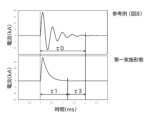
図8は、図6に示した参考例としての電気パルス発生装置71を用い、コンデンサ11に対して高電圧源5からの出力電圧によって充電を完了した後、スイッチング素子13を導通させた後の通電対象物3に流れる電流iZと、通電対象物3の両端電圧の挙動を示すグラフの一例である。図8によれば、数ms程度の時間にわたって通電対象物3に対して電流が流れている。なお、図8における回路条件は以下の通りであり、フラッシュランプを通電対象物3とした場合の参考例である。
インダクタンス成分(図1におけるインダクタ17と同義):12μH
通電対象物3の抵抗値:50mΩ
コンデンサ11の容量:400μF
コンデンサ11の充電電圧:4000V
インダクタンス成分(図1におけるインダクタ17と同義):12μH
通電対象物3の抵抗値:50mΩ
コンデンサ11の容量:400μF
コンデンサ11の充電電圧:4000V
図8のグラフにおいても、通電対象物3に対して電流が流れる時間は、高々数ms程度であり、1秒より十分短い時間である。このため、参考例の電気パルス発生装置71においても、通電対象物3に対して瞬時的な電流が流れているとも思える。しかし、本発明者らは、電気パルス発生装置71よりも更に電流のパルス幅を狭めることができれば、以下が可能になると想起した。
(1)通電対象物3をフラッシュランプ7とした場合には、短いパルス幅にすることでフラッシュランプ7の発光効率を高めつつ、加熱対象物30の表面領域31の加熱の制御が改善する。
逆に、フラッシュランプ7に対して電流iZが流れる時間が長くすると、プラズマの生成効率が下がるとともに、加熱対象物30への光の照射時間も長くなる。すると、図9Aにおいてハッチング領域で示されるように、加熱対象物30の表面領域31のみならず、それよりも深い位置の下層32にまで熱が到達し、加熱されてしまう。この結果、下層32にダメージが生じるおそれがある(図9A参照)。
(2)通電対象物3を複合構造物4とした場合には、短いパルス幅にすることで加熱対象物30の加熱の制御性が向上し、分離効率を上げることができる。
逆に、複合構造物4に対して電流iZが流れる時間が長くなると、金属板41の一部が過剰に加熱され、破断して蒸発し(金属板の部分41a,41b)、離脱した構成材料43aに付着・混入してしまい、再利用に適さないことが起こり得る(図9B参照)。
なお、上述したように、本実施形態において、スイッチング素子13は、半導体素子であるものとした。上述したように、高電圧源5を通じてkVオーダーの電圧によって充電されたコンデンサ11からの放電電流が、瞬時的にスイッチング素子13を通じて流れることに鑑みると、スイッチング素子13がメカニカルスイッチである場合には、電気パルス発生装置1の経時的な利用に伴って、接点が摩耗し、接点の抵抗が大きくなる恐れもある。理想上では、電流ピークの値は、通電対象物3の抵抗値より決定される(電流ピーク値=供給される高電圧/通電対象物3の抵抗値)。しかしながら、接点の摩耗により抵抗値が大きくなれば通電対象物3の抵抗値との合計値が全体の抵抗値として計算され、パルス電流のピーク値が減少する。これは、本発明で述べた課題の1つでもある、電気パルスのエネルギー量の再現性の観点からみて好ましくない。電気パルス発生装置1の長期利用に鑑みると、スイッチング素子13は半導体素子であるのが好ましい。
更に、図1に示す電気パルス発生装置1においては、負荷回路部2がインダクタ17を備えるものとした。しかし、インダクタ17を備えずに、閉回路内に存在する寄生インダクタンスを利用することも可能である。
上記のように、スイッチング素子13として利用可能な半導体スイッチには、電流の立ち上がり速度(ΔI/Δt)についての許容最大値が定格値として規定されている場合がある。あまりにも急峻な電流が半導体スイッチに流れると、半導体接合内部の電流拡散が間に合わずに、局所的に電流が集中して半導体スイッチが加熱破壊されるおそれがある。
かかる観点から、上記の、電流の立ち上がり速度の最大許容値が設けられる場合がある。
かかる観点から、上記の、電流の立ち上がり速度の最大許容値が設けられる場合がある。
この電流の立ち上がり速度を低減するためには、図1に示すように、意図的にインダクタ17を挿入することが有効である。半導体スイッチを採用することで、高い再現性を有しつつ、経時的な変化の少ない電気パルスを出力できる一方、インダクタ17を挿入することで、電流パルスの増加の傾きが低減するトレードオフが発生する。本発明の目的である、再現ある電気パルスの提供とともに、エネルギーを提供する期間を短縮することの両立を実現すべく、電気パルス発生回路に対して、更なる工夫をするのが好ましい。これについて以降より説明する。なお、以下の図面では、適宜図1内の負荷回路部2のみが図示される。
参考例としての電気パルス発生装置71と同様に、コンデンサ11への充電が完了すると、コンデンサ11の充電電圧に由来する電流iZを通電対象物3に流すために、スイッチング素子13が導通される(図10A参照)。スイッチング素子13が導通状態になると、kVオーダーの電圧に由来した電流iZが瞬時的にスイッチング素子13を介して通電対象物3に流れる。
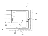
上述したように、電気パルス発生装置1の負荷回路部2は、ダイオード15を備えている。ダイオード15は、コンデンサ11が充電された状態の下で、スイッチング素子13を非導通状態から導通状態に遷移すると、カソード端子の接続点P1はアノード端子の接続点P2よりもコンデンサ11の高電位側の端子に電気的に近い位置である。このため、通電対象物3を流れた電流iZは、コンデンサ11を迂回してダイオード15を介して流れることになる(図10B参照)。言い換えれば、コンデンサ11の放電後には、ダイオード15とインダクタ17と通電対象物3とが直列に接続されて、且つコンデンサ11を含まない、第二閉回路U2が形成される。
つまり、参考例の電気パルス発生装置71とは異なり、本実施形態の電気パルス発生装置1によれば、コンデンサ11が再度逆極性の充電を行うことがないため、通電対象物3に対して電流iZが流れる時間が大幅に短縮化される。
図11は、本実施形態の電気パルス発生装置1を用い、コンデンサ11に対して高電圧源5からの出力電圧によって充電を完了した後、スイッチング素子13を導通させた後の通電対象物3に流れる電流iZと、通電対象物3の両端電圧の挙動を示すグラフの一例である。なお、図11には、比較のために、図8に示した参考例の電気パルス発生装置71における電流iZの挙動を示すグラフが併記されている。両者の波形を比較すると、本実施形態の電気パルス発生装置1によれば、通電対象物3に対して電流iZが流れる時間(τ1)は、ダイオード15がない場合(参考例)の電流iZが流れる時間(τ0)に比べて、短縮化できていることが理解される。
なお、図11における回路条件は以下の通りである。すなわち、図11における回路条件は、ダイオード15が存在している点を除き、図8における回路条件と共通している。
以下の数値は、フラッシュランプを通電対象物3とした場合の参考例である。
インダクタンス成分(図1におけるインダクタ17と同義):12μH
通電対象物3の抵抗値:50mΩ
コンデンサ11の容量:400μF
コンデンサ11の充電電圧:4000V
ダイオード15:あり
以下の数値は、フラッシュランプを通電対象物3とした場合の参考例である。
インダクタンス成分(図1におけるインダクタ17と同義):12μH
通電対象物3の抵抗値:50mΩ
コンデンサ11の容量:400μF
コンデンサ11の充電電圧:4000V
ダイオード15:あり
より詳細には、通電対象物3に流れる電流iZは、ピーク電流の後に流れるピーク電流の電流値の10%未満のリンギング電流を含むことがある。このリンギング電流は回路内のある寄生インダクタンスが関係している。ただし、ピーク電流の発生タイミングから電流がゼロ近傍に移行するタイミング迄の間において、極性を変化させることなく実質的に逓減している。電流波形が実質的な逓減を開始するまでの時間幅である主パルス幅の期間(τ1)は、1.2ms程度という短い時間であることが確認される。期間(τ1)の後の期間(τ3)においても、ピーク電流の電流値の10%未満のリンギング電流が引き続き確認できる場合もあるが、この程度であれば加熱に対して大きな影響はないと考えることができる。
図12~図14は、本実施形態の電気パルス発生装置1に含まれる負荷回路部2の別構成例を、図10Bにならって模式的に示す回路図である。すなわち、図12~図14は、いずれも、コンデンサ11の放電が完了した後の電流iZの挙動が示されている。
いずれの回路方式においても、コンデンサ11への充電時においては、コンデンサ11と、通電対象物3と、スイッチング素子13と、インダクタ17とを含む直列回路(第一閉回路U1)が形成される。そして、コンデンサ11が充電された状態の下で、スイッチング素子13を非導通状態から導通状態に遷移すると、通電対象物3を流れた電流iZは、コンデンサ11を迂回してダイオード15を介して流れる。コンデンサ11の放電後には、ダイオード15とインダクタ17と通電対象物3とが直列に接続されて、且つコンデンサ11を含まない、第二閉回路U2が形成される。
以上説明したように、本実施形態の電気パルス発生装置1によれば、短パルスが実現されるため、通電対象物3と加熱対象物30のダメージを低減しつつ、加熱対象物30を効率良く、適切な範囲で再現よく加熱することができる。
[第二実施形態]
本発明に係る電気パルス発生装置の第二実施形態について、主として第一実施形態と異なる箇所を説明する。なお、第一実施形態と共通の要素については、同一の符号が付されることで、その説明が簡素化又は省略される。
本発明に係る電気パルス発生装置の第二実施形態について、主として第一実施形態と異なる箇所を説明する。なお、第一実施形態と共通の要素については、同一の符号が付されることで、その説明が簡素化又は省略される。
図15は、本実施形態の電気パルス発生装置1の構成を図1にならって模式的に示す回路ブロック図である。本実施形態の電気パルス発生装置1は、第一実施形態と比較して、負荷回路部2の構成が異なっている。具体的には、ダイオード15が、通電対象物3及びコンデンサ11の直列回路に対して並列に接続されている点が異なっている。
本実施形態の電気パルス発生装置1の動作について図16A及び図16Bを参照して説明する。図16A及び図16Bは、図10A及び図10Bにならって、本実施形態の電気パルス発生装置1の負荷回路部2のみが抽出されている。
コンデンサ11への充電が完了すると、コンデンサ11の充電電圧に由来する電流iZを通電対象物3に流すために、スイッチング素子13が導通される(図16A参照)。スイッチング素子13が導通状態になると、kVオーダーの電圧に由来した電流iZが瞬時的にスイッチング素子13を介して通電対象物3に流れる。
本実施形態の電気パルス発生装置1の負荷回路部2も、第一実施形態と同様にダイオード15を備えている。ダイオード15は、コンデンサ11が充電された状態の下で、スイッチング素子13を非導通状態から導通状態に遷移すると、カソード端子の接続点P1はアノード端子の接続点P2よりもコンデンサ11の高電位側の端子に電気的に近い位置である。このため、通電対象物3を流れた電流iZは、コンデンサ11及び通電対象物3を迂回してダイオード15を介して流れることになる(図16B参照)。言い換えれば、コンデンサ11の放電後には、ダイオード15とインダクタ17とが直列に接続されて、且つコンデンサ11と通電対象物3とを含まない、第二閉回路U2が形成される。
つまり、本実施形態の電気パルス発生装置1においても、コンデンサ11が逆極性の充電を行うことがないため、通電対象物3に対して電流iZが流れる時間が大幅に短縮化される。更に、第一実施形態と比較しても、通電対象物3に対して電流iZが流れる時間を更に短縮化できる。
なお、図16A~図16Bを参照して上述したように、本実施形態の電気パルス発生装置1の構成においては、通電対象物3を介してコンデンサ11への充電が行われる。ここで、図2を参照して上述したように、通電対象物3がフラッシュランプ7である場合、フラッシュランプ7は点灯を開始するまでは絶縁性を示すため、この期間は通電対象物3が実質的に絶縁性を示すことになる。この場合、通電対象物3を介してコンデンサ11に充電を行うことができない。かかる観点から、コンデンサ11への充電経路を確保するため、通電対象物3(ここではフラッシュランプ7)に並列に、数Ω程度の抵抗を接続しても構わない。また、充電経路を確保するためのダイオードを追加しても構わない。
図17は、本実施形態の電気パルス発生装置1を用い、コンデンサ11に対して高電圧源5からの出力電圧によって充電を完了した後、スイッチング素子13を導通させた後の通電対象物3に流れる電流iZの挙動を示すグラフの一例である。なお、図17には、比較のために、図11に示した第一実施形態の電気パルス発生装置71における電流iZの挙動を示すグラフが併記されている。
図17によれば、本実施形態の電気パルス発生装置1を用いることで、第一実施形態よりも更に通電対象物3に流れる電流iZの時間が短縮化されることが確認される。図17によれば、第一実施形態の電気パルス発生装置1の場合には、ピーク電流の発生タイミングから電流が逓減を開始するタイミング迄の時間幅である主パルス幅の期間(τ1)が1.2ms程度であったのに対し、本実施形態の場合の期間(τ2)は0.2ms程度である。つまり、図17に加えて、図11も参照すれば、本実施形態の電気パルス発生装置1によれば、参考例の電気パルス発生装置71とくらべて、パルス幅の期間を大幅に短くできていることが分かる。
本実施形態の電気パルス発生装置1では、図15に示すように、ダイオード15が、コンデンサ11と通電対象物3との接続回路に対して並列に配置されている点が特徴である。コンデンサ11、通電対象物3、及びダイオード15を、それぞれ可能な限り近くに配置することで、第二閉回路U2内にある回路上のインダクタ17以外の寄生インダクンス由来の電流の発現が抑制される。この結果、本実施形態の電気パルス発生装置1によれば、図17に示すように、主パルスが発生した後には、ほとんどリンギング電流が流れない。
図18~図19は、本実施形態の電気パルス発生装置1に含まれる負荷回路部2の別構成例を、図16Bにならって模式的に示す回路図である。すなわち、図18~図19は、いずれも、コンデンサ11の放電が完了した後の電流iZの挙動が示されている。
いずれの回路においても、コンデンサ11への充電時においては、コンデンサ11と、通電対象物3と、スイッチング素子13と、インダクタ17とを含む直列回路(第一閉回路U1)が形成される。そして、コンデンサ11が充電された状態の下で、スイッチング素子13を非導通状態から導通状態に遷移すると、通電対象物3を流れた電流iZは、コンデンサ11及び通電対象物3を迂回してダイオード15を介して流れる。コンデンサ11の放電後には、ダイオード15とインダクタ17とが直列に接続されて、且つコンデンサ11と通電対象物3とを含まない、第二閉回路U2が形成される。
以上説明したように、本実施形態の電気パルス発生装置1によれば、第一実施形態とくらべて更にパルス幅の期間が短い電気パルスが実現されるため、通電対象物3と加熱対象物30のダメージを低減しつつ、加熱対象物30を効率良く、適切な範囲で再現よく加熱することができる。
[第三実施形態]
本発明に係る電気パルス発生装置の第三実施形態について、主として第一実施形態と異なる箇所を説明する。なお、第一実施形態と共通の要素については、同一の符号が付されることで、その説明が簡素化又は省略される。
本発明に係る電気パルス発生装置の第三実施形態について、主として第一実施形態と異なる箇所を説明する。なお、第一実施形態と共通の要素については、同一の符号が付されることで、その説明が簡素化又は省略される。
図20は、本実施形態の電気パルス発生装置1の構成を図1にならって模式的に示す回路ブロック図である。本実施形態の電気パルス発生装置1は、第一実施形態と比較して、負荷回路部2の構成が異なっている。具体的には、ダイオード15がインダクタ17に対して並列に接続されている点が異なっている。
本実施形態の電気パルス発生装置1の動作について図21A及び図21Bを参照して説明する。図21A及び図21Bは、図10A及び図10Bにならって、本実施形態の電気パルス発生装置1の負荷回路部2のみが抽出されている。
コンデンサ11への充電が完了すると、コンデンサ11の充電電圧に由来する電流iZを通電対象物3に流すために、スイッチング素子13が導通される(図21A参照)。スイッチング素子13が導通状態になると、kVオーダーの電圧に由来した電流iZが瞬時的にスイッチング素子13を介して通電対象物3に流れる。
本実施形態の電気パルス発生装置1の負荷回路部2も、第一実施形態と同様にダイオード15を備えている。ダイオード15は、コンデンサ11が充電された状態の下で、スイッチング素子13を非導通状態から導通状態に遷移すると、カソード端子の接続点P1はアノード端子の接続点P2よりもコンデンサ11の高電位側の端子に電気的に近い位置である。このため、図21Aの時点では、コンデンサ11からの電流iZはダイオード15を介さず、インダクタ17を介して通電対象物3に流れる。その後、インダクタ17からの誘導電流が発生すると、接続点P2からダイオード15を介して接続点P1に向かう電流iZが流れる(図21B参照)。通電対象物3に向かう電流iZが瞬時的に流れた後は、もはや通電対象物3側には電流が流れず、インダクタ17とダイオード15とで形成される第二閉回路U2内を電流が流れることになる。
つまり、本実施形態においても、第二実施形態と同様、コンデンサ11の放電後には、ダイオード15とインダクタ17とが直列に接続されて、且つコンデンサ11と通電対象物3とを含まない、第二閉回路U2が形成される。
以上により、本実施形態の電気パルス発生装置1においても、通電対象物3に対して電流iZが流れる時間を第一実施形態よりも更に短縮化できる。
ただし、本実施形態の電気パルス発生装置1においては、第一閉回路U1内の寄生インダクタンスに由来する電流が通電対象物3に流れる結果、10%以下程度のリンギング電流が減衰しながら引き続き電流が流れる場合がある。この場合、通電対象物3に流れる電流は現実的にはゼロにはならない。この点は、図1等を参照して上述した、第一実施形態の電気パルス発生装置1においても同様である。これに対し、図15等を参照して上述した第二実施形態の電気パルス発生装置1においては、ダイオード15によって、通電対象物3を流れる電流経路がバイパスされているため、通電対象物3を流れる電流をほぼゼロにすることが可能となる。
図22~図24は、本実施形態の電気パルス発生装置1に含まれる負荷回路部2の別構成例を、図21Bにならって模式的に示す回路図である。すなわち、図22~図24は、いずれも、コンデンサ11の放電が完了した後の電流iZの挙動が示されている。
いずれの回路においても、コンデンサ11への充電時においては、コンデンサ11と、通電対象物3と、スイッチング素子13と、インダクタ17とを含む直列回路(第一閉回路U1)が形成される。そして、コンデンサ11が充電された状態の下で、スイッチング素子13を非導通状態から導通状態に遷移すると、電流iZが通電対象物3に瞬時的に流れた後、インダクタ17の誘導電流が、ダイオード15とインダクタ17とが直列に接続されて、且つコンデンサ11と通電対象物3とを含まない、第二閉回路U2内を流れる。
以上説明したように、本実施形態の電気パルス発生装置1によれば、短パルスが実現されるため、通電対象物3と加熱対象物30のダメージを低減しつつ、加熱対象物30を効率良く、適切な範囲で再現よく加熱することができる。
以上の説明により、各実施形態の電気パルス発生装置1によれば、出力されるエネルギーのばらつきや変動を抑制しつつ、電気パルスの提供期間が短縮化できることが理解される。
実際に実験をして確認したところ、図2を参照して上述したように、通電対象物3がフラッシュランプ7である場合には、電気パルス発生装置1を用いてフラッシュランプ7を点灯することにより、フラッシュランプ7の発光効率を向上させつつ、加熱対象物30に対する加熱深度の制御が可能になることが確認された。また、図3を参照して上述したように、通電対象物3と加熱対象物30とが一体化された複合構造物4に対して、電気パルス発生装置1を用いて電気パルスを供給した場合においても、原理的には同一であり、加熱対象物30に対する加熱深度を制御することにより、より高い精度で層の分離が期待できるだろう。
本発明は上記した実施形態に限定されるものではなく、様々な変形例が含まれる。例えば、上記した実施形態は本発明のより良い理解のために詳細に説明したのであり、必ずしも説明の全ての構成を備えるものに限定されるものではない。本発明の範囲は特許請求の範囲によって示され、特許請求の範囲と均等の意味及び範囲内での全ての変更が含まれることが意図される。
1 :電気パルス発生装置
2 :負荷回路部
3 :通電対象物
4 :複合構造物
5 :高電圧源
6 :スイッチング素子
7 :フラッシュランプ
11 :コンデンサ
13 :スイッチング素子
15 :ダイオード
17 :インダクタ
23 :発光管
30 :加熱対象物
31 :加熱対象物の表面領域
32 :下層
33 :ネジ部材
41 :金属板
41a,41b :金属板に由来する部分
43 :構成材料
45 :構成材料
47 :上部金属電極
48 :有機薄膜層
49 :透明電極層
51 :電極
52 :電極
55 :導電性の溶液
56 :収容容器
71 :参考例の電気パルス発生装置
72 :負荷回路部
90 :通電対象物
91 :コンデンサ
92 :メカニカルスイッチ
95 :高電圧源
96 :スイッチング素子
100 :従来例の電気パルス発生装置
L7 :光
P1 :接続点
P2 :接続点
U1 :第一閉回路
U2 :第二閉回路
iZ :電流
τ0~τ3: 期間
2 :負荷回路部
3 :通電対象物
4 :複合構造物
5 :高電圧源
6 :スイッチング素子
7 :フラッシュランプ
11 :コンデンサ
13 :スイッチング素子
15 :ダイオード
17 :インダクタ
23 :発光管
30 :加熱対象物
31 :加熱対象物の表面領域
32 :下層
33 :ネジ部材
41 :金属板
41a,41b :金属板に由来する部分
43 :構成材料
45 :構成材料
47 :上部金属電極
48 :有機薄膜層
49 :透明電極層
51 :電極
52 :電極
55 :導電性の溶液
56 :収容容器
71 :参考例の電気パルス発生装置
72 :負荷回路部
90 :通電対象物
91 :コンデンサ
92 :メカニカルスイッチ
95 :高電圧源
96 :スイッチング素子
100 :従来例の電気パルス発生装置
L7 :光
P1 :接続点
P2 :接続点
U1 :第一閉回路
U2 :第二閉回路
iZ :電流
τ0~τ3: 期間
Claims (8)
- 通電対象物に対して電気パルスを印加する電気パルス発生装置であって、
高電圧源と、前記高電圧源からの出力電圧を印加可能に配置された負荷回路部とを備え、
前記負荷回路部は、
前記通電対象物と、
前記通電対象物に対して直列に接続されたスイッチング素子と、
前記高電圧源と前記負荷回路部とが電気的に接続されると前記高電圧源からの出力電圧に基づいて充電可能な位置に配置されたコンデンサと、
アノード端子及びカソード端子を含むダイオードとを有し、
前記負荷回路部は、前記スイッチング素子が導通状態の下で、前記コンデンサと、前記通電対象物と、前記スイッチング素子とを含む直列回路である第一閉回路を形成し、
前記ダイオードは、前記アノード端子及び前記カソード端子が、それぞれ前記第一閉回路上の2箇所に接続されており、
前記コンデンサが充電された状態の下で前記スイッチング素子を非導通状態から導通状態に遷移させた時点において、前記カソード端子と前記第一閉回路との接続点が、前記アノード端子と前記第一閉回路との接続点よりも、前記コンデンサの高電位側の端子に電気的に近い位置に配置されていることを特徴とする、電気パルス発生装置。 - 前記高電圧源と前記負荷回路部とが電気的に接続されたときに前記通電対象物に流れる負荷電流は、ピーク電流と、前記ピーク電流の後に流れる前記ピーク電流の電流値の10%未満のリンギング電流とを含み、
前記負荷電流は、前記ピーク電流の発生タイミングから前記リンギング電流の発生タイミング迄の間において、極性を変化させることなく実質的に逓減することを特徴とする、請求項1に記載の電気パルス発生装置。 - 前記負荷電流は、前記ピーク電流の発生タイミングから前記リンギング電流の発生タイミング迄の時間幅である主パルス幅が1.2ms以下であることを特徴とする、請求項2に記載の電気パルス発生装置。
- 前記負荷回路部はインダクタを含み、
前記第一閉回路は、前記コンデンサと、前記通電対象物と、前記スイッチング素子と、前記インダクタとを含む直列回路であることを特徴とする、請求項1~3のいずれか1項に記載の電気パルス発生装置。 - 前記負荷回路部は、前記コンデンサの放電後に、直列に接続された前記ダイオードと前記インダクタと前記通電対象物とを含み、且つ前記コンデンサを含まない、第二閉回路を形成することを特徴とする、請求項4に記載の電気パルス発生装置。
- 前記負荷回路部は、前記コンデンサの放電後に、直列に接続された前記ダイオードと前記インダクタとを含み、且つ前記コンデンサ及び前記通電対象物を含まない、第二閉回路を形成することを特徴とする、請求項4に記載の電気パルス発生装置。
- 前記スイッチング素子は、半導体素子からなることを特徴とする、請求項1~3のいずれか1項に記載の電気パルス発生装置。
- 前記通電対象物は、フラッシュランプであることを特徴とする、請求項1~3のいずれか1項に記載の電気パルス発生装置。
Applications Claiming Priority (2)
| Application Number | Priority Date | Filing Date | Title |
|---|---|---|---|
| JP2023103589A JP2025003103A (ja) | 2023-06-23 | 2023-06-23 | 電気パルス発生装置 |
| JP2023-103589 | 2023-06-23 |
Publications (1)
| Publication Number | Publication Date |
|---|---|
| WO2024262148A1 true WO2024262148A1 (ja) | 2024-12-26 |
Family
ID=93935543
Family Applications (1)
| Application Number | Title | Priority Date | Filing Date |
|---|---|---|---|
| PCT/JP2024/015212 Ceased WO2024262148A1 (ja) | 2023-06-23 | 2024-04-17 | 電気パルス発生装置 |
Country Status (3)
| Country | Link |
|---|---|
| JP (1) | JP2025003103A (ja) |
| TW (1) | TW202501986A (ja) |
| WO (1) | WO2024262148A1 (ja) |
Citations (3)
| Publication number | Priority date | Publication date | Assignee | Title |
|---|---|---|---|---|
| JPH04296834A (ja) * | 1991-01-09 | 1992-10-21 | Heimann Gmbh | フラッシュランプ及びその点灯回路 |
| JPH08160509A (ja) * | 1994-12-07 | 1996-06-21 | Canon Inc | ストロボ装置 |
| JP2009164201A (ja) * | 2007-12-28 | 2009-07-23 | Ushio Inc | 基板加熱装置及び基板加熱方法 |
-
2023
- 2023-06-23 JP JP2023103589A patent/JP2025003103A/ja active Pending
-
2024
- 2024-04-17 WO PCT/JP2024/015212 patent/WO2024262148A1/ja not_active Ceased
- 2024-05-23 TW TW113119064A patent/TW202501986A/zh unknown
Patent Citations (3)
| Publication number | Priority date | Publication date | Assignee | Title |
|---|---|---|---|---|
| JPH04296834A (ja) * | 1991-01-09 | 1992-10-21 | Heimann Gmbh | フラッシュランプ及びその点灯回路 |
| JPH08160509A (ja) * | 1994-12-07 | 1996-06-21 | Canon Inc | ストロボ装置 |
| JP2009164201A (ja) * | 2007-12-28 | 2009-07-23 | Ushio Inc | 基板加熱装置及び基板加熱方法 |
Also Published As
| Publication number | Publication date |
|---|---|
| TW202501986A (zh) | 2025-01-01 |
| JP2025003103A (ja) | 2025-01-09 |
Similar Documents
| Publication | Publication Date | Title |
|---|---|---|
| US20110038187A1 (en) | Bipolar pulsed power supply and power supply apparatus having plurality of bipolar pulsed power supplies | |
| CN102111946B (zh) | 放电灯点亮装置 | |
| CN102333623A (zh) | 在基板上产生孔或凹陷或井的方法、执行所述方法的器件以及在这种器件中使用的高频高电压源 | |
| US8680764B2 (en) | Method of manufacturing organic EL device and organic EL device | |
| JP5532720B2 (ja) | 同軸磁化プラズマ生成装置 | |
| JP5186281B2 (ja) | バイポーラパルス電源及びこのバイポーラパルス電源を複数台並列接続してなる電源装置 | |
| CN113484766B (zh) | 保险主动熔断电路、装置和电池组件 | |
| JP6368928B2 (ja) | 直流スパッタ装置用電源装置 | |
| JP2025003103A (ja) | 電気パルス発生装置 | |
| CN114033597B (zh) | 一种基于纳秒脉冲放电的大体积点火系统 | |
| Ahn et al. | Design and implementation of 3-kW simmer and 30-kV DC trigger power supply system for driving xenon flash lamps in large-area processes | |
| US9522436B2 (en) | System for converting electric energy into thermal energy | |
| KR20010074908A (ko) | 유전적인 방해 방전을 포함하는 방전 램프용 전자 안정기 | |
| CN102860135A (zh) | 启动气体放电灯的方法和控制电路 | |
| EP1194018A2 (en) | Inter-torch plasma transfer device | |
| JP2008253096A (ja) | 放電負荷用電源 | |
| JP7277144B2 (ja) | 基層を熱処理する方法及び装置 | |
| US20170273167A1 (en) | Plasma-Containing Modular Arc Generator | |
| KR102943689B1 (ko) | 플래시 램프 제어 방법 및 배열체 | |
| Cho et al. | Integrated 15-kV DC trigger and simmer power supply for light sintering | |
| US10812020B1 (en) | Energy emitter control circuit | |
| WO2025134516A1 (ja) | 閃光照射装置 | |
| JP2016054043A (ja) | 安定器 | |
| CN105207648B (zh) | 一种脉冲二极管、其制备方法以及产生电脉冲的方法 | |
| KR20000074546A (ko) | 압전/전왜 액튜에이터를 이용한 형광등 점등장치 |
Legal Events
| Date | Code | Title | Description |
|---|---|---|---|
| 121 | Ep: the epo has been informed by wipo that ep was designated in this application |
Ref document number: 24825558 Country of ref document: EP Kind code of ref document: A1 |
|
| NENP | Non-entry into the national phase |
Ref country code: DE |