WO2024262020A1 - 空間光変調ユニットおよび露光装置 - Google Patents
空間光変調ユニットおよび露光装置 Download PDFInfo
- Publication number
- WO2024262020A1 WO2024262020A1 PCT/JP2023/023359 JP2023023359W WO2024262020A1 WO 2024262020 A1 WO2024262020 A1 WO 2024262020A1 JP 2023023359 W JP2023023359 W JP 2023023359W WO 2024262020 A1 WO2024262020 A1 WO 2024262020A1
- Authority
- WO
- WIPO (PCT)
- Prior art keywords
- light
- dmd
- illumination
- opening
- exposure apparatus
- Prior art date
- Legal status (The legal status is an assumption and is not a legal conclusion. Google has not performed a legal analysis and makes no representation as to the accuracy of the status listed.)
- Ceased
Links
Images











Classifications
-
- G—PHYSICS
- G03—PHOTOGRAPHY; CINEMATOGRAPHY; ANALOGOUS TECHNIQUES USING WAVES OTHER THAN OPTICAL WAVES; ELECTROGRAPHY; HOLOGRAPHY
- G03F—PHOTOMECHANICAL PRODUCTION OF TEXTURED OR PATTERNED SURFACES, e.g. FOR PRINTING, FOR PROCESSING OF SEMICONDUCTOR DEVICES; MATERIALS THEREFOR; ORIGINALS THEREFOR; APPARATUS SPECIALLY ADAPTED THEREFOR
- G03F7/00—Photomechanical, e.g. photolithographic, production of textured or patterned surfaces, e.g. printing surfaces; Materials therefor, e.g. comprising photoresists; Apparatus specially adapted therefor
- G03F7/70—Microphotolithographic exposure; Apparatus therefor
- G03F7/70216—Mask projection systems
- G03F7/70283—Mask effects on the imaging process
- G03F7/70291—Addressable masks, e.g. spatial light modulators [SLMs], digital micro-mirror devices [DMDs] or liquid crystal display [LCD] patterning devices
-
- G—PHYSICS
- G02—OPTICS
- G02B—OPTICAL ELEMENTS, SYSTEMS OR APPARATUS
- G02B26/00—Optical devices or arrangements for the control of light using movable or deformable optical elements
- G02B26/08—Optical devices or arrangements for the control of light using movable or deformable optical elements for controlling the direction of light
- G02B26/0816—Optical devices or arrangements for the control of light using movable or deformable optical elements for controlling the direction of light by means of one or more reflecting elements
- G02B26/0833—Optical devices or arrangements for the control of light using movable or deformable optical elements for controlling the direction of light by means of one or more reflecting elements the reflecting element being a micromechanical device, e.g. a MEMS mirror, DMD
- G02B26/0841—Optical devices or arrangements for the control of light using movable or deformable optical elements for controlling the direction of light by means of one or more reflecting elements the reflecting element being a micromechanical device, e.g. a MEMS mirror, DMD the reflecting element being moved or deformed by electrostatic means
-
- G—PHYSICS
- G02—OPTICS
- G02B—OPTICAL ELEMENTS, SYSTEMS OR APPARATUS
- G02B26/00—Optical devices or arrangements for the control of light using movable or deformable optical elements
- G02B26/08—Optical devices or arrangements for the control of light using movable or deformable optical elements for controlling the direction of light
- G02B26/10—Scanning systems
-
- G—PHYSICS
- G03—PHOTOGRAPHY; CINEMATOGRAPHY; ANALOGOUS TECHNIQUES USING WAVES OTHER THAN OPTICAL WAVES; ELECTROGRAPHY; HOLOGRAPHY
- G03F—PHOTOMECHANICAL PRODUCTION OF TEXTURED OR PATTERNED SURFACES, e.g. FOR PRINTING, FOR PROCESSING OF SEMICONDUCTOR DEVICES; MATERIALS THEREFOR; ORIGINALS THEREFOR; APPARATUS SPECIALLY ADAPTED THEREFOR
- G03F7/00—Photomechanical, e.g. photolithographic, production of textured or patterned surfaces, e.g. printing surfaces; Materials therefor, e.g. comprising photoresists; Apparatus specially adapted therefor
- G03F7/20—Exposure; Apparatus therefor
-
- G—PHYSICS
- G03—PHOTOGRAPHY; CINEMATOGRAPHY; ANALOGOUS TECHNIQUES USING WAVES OTHER THAN OPTICAL WAVES; ELECTROGRAPHY; HOLOGRAPHY
- G03F—PHOTOMECHANICAL PRODUCTION OF TEXTURED OR PATTERNED SURFACES, e.g. FOR PRINTING, FOR PROCESSING OF SEMICONDUCTOR DEVICES; MATERIALS THEREFOR; ORIGINALS THEREFOR; APPARATUS SPECIALLY ADAPTED THEREFOR
- G03F7/00—Photomechanical, e.g. photolithographic, production of textured or patterned surfaces, e.g. printing surfaces; Materials therefor, e.g. comprising photoresists; Apparatus specially adapted therefor
- G03F7/70—Microphotolithographic exposure; Apparatus therefor
- G03F7/70058—Mask illumination systems
- G03F7/70075—Homogenization of illumination intensity in the mask plane by using an integrator, e.g. fly's eye lens, facet mirror or glass rod, by using a diffusing optical element or by beam deflection
-
- G—PHYSICS
- G03—PHOTOGRAPHY; CINEMATOGRAPHY; ANALOGOUS TECHNIQUES USING WAVES OTHER THAN OPTICAL WAVES; ELECTROGRAPHY; HOLOGRAPHY
- G03F—PHOTOMECHANICAL PRODUCTION OF TEXTURED OR PATTERNED SURFACES, e.g. FOR PRINTING, FOR PROCESSING OF SEMICONDUCTOR DEVICES; MATERIALS THEREFOR; ORIGINALS THEREFOR; APPARATUS SPECIALLY ADAPTED THEREFOR
- G03F7/00—Photomechanical, e.g. photolithographic, production of textured or patterned surfaces, e.g. printing surfaces; Materials therefor, e.g. comprising photoresists; Apparatus specially adapted therefor
- G03F7/70—Microphotolithographic exposure; Apparatus therefor
- G03F7/70058—Mask illumination systems
- G03F7/70091—Illumination settings, i.e. intensity distribution in the pupil plane or angular distribution in the field plane; On-axis or off-axis settings, e.g. annular, dipole or quadrupole settings; Partial coherence control, i.e. sigma or numerical aperture [NA]
- G03F7/70116—Off-axis setting using a programmable means, e.g. liquid crystal display [LCD], digital micromirror device [DMD] or pupil facets
-
- G—PHYSICS
- G03—PHOTOGRAPHY; CINEMATOGRAPHY; ANALOGOUS TECHNIQUES USING WAVES OTHER THAN OPTICAL WAVES; ELECTROGRAPHY; HOLOGRAPHY
- G03F—PHOTOMECHANICAL PRODUCTION OF TEXTURED OR PATTERNED SURFACES, e.g. FOR PRINTING, FOR PROCESSING OF SEMICONDUCTOR DEVICES; MATERIALS THEREFOR; ORIGINALS THEREFOR; APPARATUS SPECIALLY ADAPTED THEREFOR
- G03F7/00—Photomechanical, e.g. photolithographic, production of textured or patterned surfaces, e.g. printing surfaces; Materials therefor, e.g. comprising photoresists; Apparatus specially adapted therefor
- G03F7/70—Microphotolithographic exposure; Apparatus therefor
- G03F7/70058—Mask illumination systems
- G03F7/70141—Illumination system adjustment, e.g. adjustments during exposure or alignment during assembly of illumination system
-
- G—PHYSICS
- G03—PHOTOGRAPHY; CINEMATOGRAPHY; ANALOGOUS TECHNIQUES USING WAVES OTHER THAN OPTICAL WAVES; ELECTROGRAPHY; HOLOGRAPHY
- G03F—PHOTOMECHANICAL PRODUCTION OF TEXTURED OR PATTERNED SURFACES, e.g. FOR PRINTING, FOR PROCESSING OF SEMICONDUCTOR DEVICES; MATERIALS THEREFOR; ORIGINALS THEREFOR; APPARATUS SPECIALLY ADAPTED THEREFOR
- G03F7/00—Photomechanical, e.g. photolithographic, production of textured or patterned surfaces, e.g. printing surfaces; Materials therefor, e.g. comprising photoresists; Apparatus specially adapted therefor
- G03F7/70—Microphotolithographic exposure; Apparatus therefor
- G03F7/70058—Mask illumination systems
- G03F7/7015—Details of optical elements
-
- G—PHYSICS
- G03—PHOTOGRAPHY; CINEMATOGRAPHY; ANALOGOUS TECHNIQUES USING WAVES OTHER THAN OPTICAL WAVES; ELECTROGRAPHY; HOLOGRAPHY
- G03F—PHOTOMECHANICAL PRODUCTION OF TEXTURED OR PATTERNED SURFACES, e.g. FOR PRINTING, FOR PROCESSING OF SEMICONDUCTOR DEVICES; MATERIALS THEREFOR; ORIGINALS THEREFOR; APPARATUS SPECIALLY ADAPTED THEREFOR
- G03F7/00—Photomechanical, e.g. photolithographic, production of textured or patterned surfaces, e.g. printing surfaces; Materials therefor, e.g. comprising photoresists; Apparatus specially adapted therefor
- G03F7/70—Microphotolithographic exposure; Apparatus therefor
- G03F7/70058—Mask illumination systems
- G03F7/70191—Optical correction elements, filters or phase plates for controlling intensity, wavelength, polarisation, phase or the like
-
- G—PHYSICS
- G03—PHOTOGRAPHY; CINEMATOGRAPHY; ANALOGOUS TECHNIQUES USING WAVES OTHER THAN OPTICAL WAVES; ELECTROGRAPHY; HOLOGRAPHY
- G03F—PHOTOMECHANICAL PRODUCTION OF TEXTURED OR PATTERNED SURFACES, e.g. FOR PRINTING, FOR PROCESSING OF SEMICONDUCTOR DEVICES; MATERIALS THEREFOR; ORIGINALS THEREFOR; APPARATUS SPECIALLY ADAPTED THEREFOR
- G03F7/00—Photomechanical, e.g. photolithographic, production of textured or patterned surfaces, e.g. printing surfaces; Materials therefor, e.g. comprising photoresists; Apparatus specially adapted therefor
- G03F7/70—Microphotolithographic exposure; Apparatus therefor
- G03F7/70058—Mask illumination systems
- G03F7/70208—Multiple illumination paths, e.g. radiation distribution devices, microlens illumination systems, multiplexers or demultiplexers for single or multiple projection systems
-
- G—PHYSICS
- G03—PHOTOGRAPHY; CINEMATOGRAPHY; ANALOGOUS TECHNIQUES USING WAVES OTHER THAN OPTICAL WAVES; ELECTROGRAPHY; HOLOGRAPHY
- G03F—PHOTOMECHANICAL PRODUCTION OF TEXTURED OR PATTERNED SURFACES, e.g. FOR PRINTING, FOR PROCESSING OF SEMICONDUCTOR DEVICES; MATERIALS THEREFOR; ORIGINALS THEREFOR; APPARATUS SPECIALLY ADAPTED THEREFOR
- G03F7/00—Photomechanical, e.g. photolithographic, production of textured or patterned surfaces, e.g. printing surfaces; Materials therefor, e.g. comprising photoresists; Apparatus specially adapted therefor
- G03F7/70—Microphotolithographic exposure; Apparatus therefor
- G03F7/70216—Mask projection systems
- G03F7/70258—Projection system adjustments, e.g. adjustments during exposure or alignment during assembly of projection system
-
- G—PHYSICS
- G03—PHOTOGRAPHY; CINEMATOGRAPHY; ANALOGOUS TECHNIQUES USING WAVES OTHER THAN OPTICAL WAVES; ELECTROGRAPHY; HOLOGRAPHY
- G03F—PHOTOMECHANICAL PRODUCTION OF TEXTURED OR PATTERNED SURFACES, e.g. FOR PRINTING, FOR PROCESSING OF SEMICONDUCTOR DEVICES; MATERIALS THEREFOR; ORIGINALS THEREFOR; APPARATUS SPECIALLY ADAPTED THEREFOR
- G03F7/00—Photomechanical, e.g. photolithographic, production of textured or patterned surfaces, e.g. printing surfaces; Materials therefor, e.g. comprising photoresists; Apparatus specially adapted therefor
- G03F7/70—Microphotolithographic exposure; Apparatus therefor
- G03F7/70216—Mask projection systems
- G03F7/70275—Multiple projection paths, e.g. array of projection systems, microlens projection systems or tandem projection systems
-
- G—PHYSICS
- G03—PHOTOGRAPHY; CINEMATOGRAPHY; ANALOGOUS TECHNIQUES USING WAVES OTHER THAN OPTICAL WAVES; ELECTROGRAPHY; HOLOGRAPHY
- G03F—PHOTOMECHANICAL PRODUCTION OF TEXTURED OR PATTERNED SURFACES, e.g. FOR PRINTING, FOR PROCESSING OF SEMICONDUCTOR DEVICES; MATERIALS THEREFOR; ORIGINALS THEREFOR; APPARATUS SPECIALLY ADAPTED THEREFOR
- G03F7/00—Photomechanical, e.g. photolithographic, production of textured or patterned surfaces, e.g. printing surfaces; Materials therefor, e.g. comprising photoresists; Apparatus specially adapted therefor
- G03F7/70—Microphotolithographic exposure; Apparatus therefor
- G03F7/70216—Mask projection systems
- G03F7/70316—Details of optical elements, e.g. of Bragg reflectors, extreme ultraviolet [EUV] multilayer or bilayer mirrors or diffractive optical elements
-
- G—PHYSICS
- G03—PHOTOGRAPHY; CINEMATOGRAPHY; ANALOGOUS TECHNIQUES USING WAVES OTHER THAN OPTICAL WAVES; ELECTROGRAPHY; HOLOGRAPHY
- G03F—PHOTOMECHANICAL PRODUCTION OF TEXTURED OR PATTERNED SURFACES, e.g. FOR PRINTING, FOR PROCESSING OF SEMICONDUCTOR DEVICES; MATERIALS THEREFOR; ORIGINALS THEREFOR; APPARATUS SPECIALLY ADAPTED THEREFOR
- G03F7/00—Photomechanical, e.g. photolithographic, production of textured or patterned surfaces, e.g. printing surfaces; Materials therefor, e.g. comprising photoresists; Apparatus specially adapted therefor
- G03F7/70—Microphotolithographic exposure; Apparatus therefor
- G03F7/70216—Mask projection systems
- G03F7/70358—Scanning exposure, i.e. relative movement of patterned beam and workpiece during imaging
Definitions
- step-and-repeat type projection exposure apparatus known as a stepper
- step-and-scan type projection exposure apparatus known as a scanning stepper, also called a scanner
- a scanning stepper also called a scanner
- This type of exposure apparatus projects and exposes a mask pattern for the electronic device onto a photosensitive layer applied to the surface of an exposed substrate (hereinafter simply called a substrate), such as a glass substrate, semiconductor wafer, printed wiring board, or resin film.
- a substrate such as a glass substrate, semiconductor wafer, printed wiring board, or resin film.
- an exposure device that uses a spatial light modulator (variable mask pattern generator) such as a digital mirror device (DMD) in which a large number of micromirrors that are slightly displaced are regularly arranged instead of a mask substrate (see, for example, Patent Document 1).
- a spatial light modulator variable mask pattern generator
- DMD digital mirror device
- illumination light obtained by mixing light from a laser diode (LD) with a wavelength of 375 nm and light from an LD with a wavelength of 405 nm in a multimode fiber bundle is irradiated onto the digital mirror device (DMD), and the reflected light from each of the many tilt-controlled micromirrors is projected and exposed onto the substrate via an imaging optical system and a microlens array.
- LD laser diode
- DMD digital mirror device
- the spatial light modulation unit comprises a spatial light modulator including a modulation section having a plurality of mirrors arranged two-dimensionally, a frame surrounding the modulation section, and a substrate on which the modulation section and the frame are mounted, and a cover located on the side of the spatial light modulator where light is incident on the modulation section, attached to the spatial light modulator, and restricting the incidence of light on the frame, the cover having an opening through which light is incident on the modulation section.
- the exposure apparatus includes the spatial light modulation unit, an illumination unit that illuminates the spatial light modulator with illumination light, and a stage that carries the spatial light modulator and moves within a plane parallel to the surface of the substrate.
- the exposure apparatus includes a spatial light modulator including a modulation section having a plurality of elements arranged two-dimensionally and a frame surrounding the modulation section, an illumination unit that illuminates the spatial light modulator with illumination light, a light shielding section that blocks the illumination light from entering the frame, and a projection unit that projects the light from the spatial light modulator onto an object that is scanned in the scanning direction.
- the exposure device includes a spatial light modulator including a modulation section having a plurality of elements arranged two-dimensionally and a frame body that houses the modulation section, an illumination unit that illuminates the spatial light modulator with illumination light, a projection unit that projects the light from the spatial light modulator onto an object that is scanned in the scanning direction, and a light-shielding cover that prevents light of the illumination light reflected by the frame body from traveling to the object.
- FIG. 1 is a perspective view showing the outline of the external configuration of an exposure apparatus according to the first embodiment.
- FIG. 2 is a diagram showing an example of the arrangement of DMD projection areas projected onto a substrate by each projection unit of a plurality of exposure modules.
- FIG. 3 is a diagram for explaining the state of continuous exposure by each of the four specific projection areas in FIG.
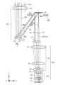
- FIG. 4 is an optical layout diagram showing a specific configuration of two exposure modules aligned in the X-axis direction (scanning exposure direction) as viewed in the XZ plane.
- FIG. 5(A) is a diagram showing a schematic diagram of a DMD
- FIG. 5(B) is a diagram showing the DMD when the power is OFF
- FIG. 5(C) is a diagram for explaining the mirror in the ON state
- FIG. 5(D) is a diagram for explaining the mirror in the OFF state
- FIG. 6A is a perspective view showing a DMD chip including a DMD
- FIG. 6B is a view showing an X'Z' cross section of the DMD chip
- FIG. 7A is a diagram of the mount portion on which the DMD chip is attached, as viewed from the -Z direction
- FIG. 7B is a diagram of the mount portion with a light-shielding cover attached.
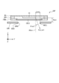
- Figure 8(A) is a cross-sectional view for explaining the arrangement of the DMD chip and the light-shielding cover
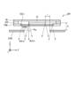
- Figure 8(B) is a cross-sectional view for explaining the size of the opening of the DMD chip and the positional relationship between the DMD chip and the opening
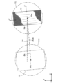
- Figures 8(C) and 8(D) are views of the DMD and opening from the -Z direction.
- FIG. 9 is a diagram for explaining the relationship between the arrangement of the aperture and the DMD, and the discarded light.
- FIG. 10 is a diagram showing a schematic diagram of a state in which the DMD and the illumination unit are tilted by an angle ⁇ k in the XY plane.
- FIG. 11 is a diagram showing another example of an opening of the light-shielding cover.
- FIG. 12 is a diagram for explaining a light-shielding cover that blocks the progression of scattered light.
- FIG. 13 is an optical layout diagram showing a specific configuration of an exposure module in the second embodiment as viewed in the XZ plane.
- FIG. 14 is a diagram for explaining in detail the imaging state of the micromirrors of the DMD by the projection unit.
- Figure 15(A) is a schematic diagram showing a projection area (a group of light irradiation areas) and an exposure target area on a substrate (an area to which a line pattern is exposed), and
- Figure 15(B) is a diagram illustrating an example of the arrangement of spot positions in the exposure target area.
- FIG. 16A is a plan view of the field stop FS, and FIG.
- FIG. 16B is a cross-sectional view taken along line AA of FIG. 16A.
- FIG. 17A is a diagram for explaining the arrangement of a field stop
- FIG. 17B is a diagram showing the illuminance distribution of illumination light formed by the field stop.
- FIG. 18A is a diagram showing an example of the illuminance distribution of illumination light
- FIG. 18B shows an example in which a rectangular region is exposed using illumination light having the illuminance distribution shown in FIG. 18A.
- FIG. 19A is a diagram for explaining how a rectangular area is exposed
- FIG. 19B is a diagram for explaining how a rectangular area is exposed when the integrated illuminance is corrected.
- FIG. 20 is a diagram illustrating a micromirror that is turned off in a DMD.
- FIG. 20 is a diagram illustrating a micromirror that is turned off in a DMD.
- FIG. 21 is a view of the substrate holder as viewed from the +Z direction.
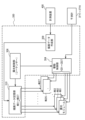
- FIG. 22 is a functional block diagram showing the functional configuration of the exposure control device.
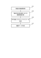
- FIG. 23 is a flowchart illustrating an example of a process executed by the drawing data generating unit.
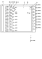
- FIG. 24A is a diagram for explaining another example of the arrangement of the field stop, and
- FIG. 24B is a diagram showing another example of the illuminance distribution of illumination light formed by the field stop.
- Figure 25(A) is a plan view showing an example of a field stop having an opening
- Figure 25(B) is a side view of the field stop
- Figure 25(C) is a cross-sectional view taken along line A-A in Figure 25(A)
- Figure 25(D) is a cross-sectional view taken along line B-B in Figure 25(B)
- Figure 25(E) is a cross-sectional view taken along line CC in Figure 25(B).
- FIG. 26A is a diagram illustrating a light-shielding cover according to a first modified example
- FIG. 26B is a diagram illustrating a light-shielding cover according to a second modified example.
- FIG. 27 is a diagram illustrating a field stop according to the third modification.
- FIG. 28 is a diagram showing a third embodiment in which pattern glass is arranged.
- 29A and 29B are diagrams showing other examples of the light blocking pattern.
- 30A and 30B are diagrams showing other examples of the light blocking pattern.
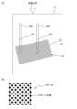
- FIG. 31 is a diagram for explaining a case where the size of the illumination field is set smaller than the size of the DMD.
- a pattern exposure apparatus (hereinafter simply referred to as an exposure apparatus) according to a first embodiment will be described with reference to the drawings.
- [Overall configuration of exposure device] 1 is a perspective view showing an outline of the external configuration of an exposure apparatus EX according to the first embodiment.
- the exposure apparatus EX is an apparatus that projects an exposure light, the intensity distribution of which in space is dynamically modulated by a spatial light modulator (SLM), onto an exposed substrate.
- SLM spatial light modulator
- Examples of spatial light modulators include a liquid crystal element, a digital micromirror device (DMD), and a magneto-optic spatial light modulator (MOSLM).
- the exposure apparatus EX according to this embodiment includes a DMD chip including a DMD 10 as a spatial light modulator, but may include other spatial light modulators.
- the exposure apparatus EX is a step-and-scan projection exposure apparatus (scanner) that exposes a rectangular (square) glass substrate used in display devices (flat panel displays) and the like.
- the glass substrate is a substrate P for flat panel displays, with at least one side or diagonal length of 500 mm or more and a thickness of 1 mm or less.
- the exposure apparatus EX exposes a projected image of a pattern created by the DMD onto a photosensitive layer (photoresist) formed with a constant thickness on the surface of the substrate P.
- the substrate P which is removed from the exposure apparatus EX after exposure, is sent to a specified process step (film formation step, etching step, plating step, etc.) after the development step.
- the exposure apparatus EX is equipped with a stage device that is composed of a pedestal 2 placed on active vibration isolation units 1a, 1b, 1c, 1d (1d not shown), a base plate 3 placed on the pedestal 2, an XY stage 4A that can move two-dimensionally on the base plate 3, a substrate holder 4B that holds a substrate P on a flat surface by suction on the XY stage 4A, and laser length measurement interferometers (hereinafter simply referred to as interferometers) IFX, IFY1 to IFY4 that measure the two-dimensional movement position of the substrate holder 4B (substrate P).
- a stage device is disclosed, for example, in U.S. Patent Publication No. 2010/0018950 and U.S. Patent Publication No. 2012/0057140.
- the XY plane of the Cartesian coordinate system XYZ is set parallel to the flat surface of the base plate 3 of the stage device, and the XY stage 4A is set so as to be able to move in translation within the XY plane.
- the direction parallel to the X axis of the coordinate system XYZ is set as the scanning movement direction of the substrate P (XY stage 4A) during scanning exposure.
- the movement position of the substrate P in the X-axis direction is measured sequentially by the interferometer IFX, and the movement position in the Y-axis direction is measured sequentially by at least one (preferably two or more) of the four interferometers IFY1 to IFY4.
- the substrate holder 4B is configured to be able to move slightly in the Z-axis direction perpendicular to the XY plane relative to the XY stage 4A, and to be able to tilt slightly in any direction relative to the XY plane, and focus adjustment and leveling (parallelism) adjustment between the surface of the substrate P and the imaging plane of the projected pattern are actively performed. Furthermore, the substrate holder 4B is configured to be able to rotate slightly ( ⁇ z rotation) around an axis parallel to the Z axis in order to actively adjust the tilt of the substrate P in the XY plane.
- the exposure apparatus EX further includes an optical base 5 that holds multiple exposure (drawing) modules MU(A), MU(B), and MU(C), and main columns 6a, 6b, 6c, and 6d (6d is not shown) that support the optical base 5 from the pedestal 2.
- Each of the multiple exposure modules MU(A), MU(B), and MU(C) is attached to the +Z direction side of the optical base 5.
- the multiple exposure modules MU(A), MU(B), and MU(C) may be attached to the optical base 5 individually, or may be attached to the optical base 5 in a state in which the rigidity is increased by connecting two or more exposure modules together.
- Each of the multiple exposure modules MU(A), MU(B), and MU(C) has an illumination unit ILU that is attached to the +Z direction side of the optical base 5 and that receives illumination light from the optical fiber unit FBU, and a projection unit PLU that is attached to the -Z direction side of the optical base 5 and has an optical axis parallel to the Z axis. Furthermore, each of the exposure modules MU(A), MU(B), and MU(C) includes a DMD 10 as a modulation unit that reflects the illumination light from the illumination unit ILU in the -Z direction and makes it incident on the projection unit PLU.
- the detailed configuration of the exposure module consisting of the illumination unit ILU, DMD 10, and projection unit PLU will be described later.
- a plurality of alignment systems (microscopes) ALG are attached to detect alignment marks formed at a plurality of predetermined positions on the substrate P.
- a calibration reference unit CU for calibration is provided at the end of the substrate holder 4B in the -X direction.
- Calibration includes at least one of the following: confirmation of the relative positional relationship in the XY plane of each detection field of the alignment system ALG, confirmation of the baseline error between each projection position of the pattern image projected from each projection unit PLU of the exposure modules MU(A), MU(B), and MU(C) and the position of each detection field of the alignment system ALG, and confirmation of the position and image quality of the pattern image projected from the projection unit PLU.
- each of the exposure modules MU(A), MU(B), and MU(C) has nine modules arranged at regular intervals in the Y-axis direction, but the number of modules may be less than or greater than nine.
- three rows of exposure modules are arranged in the X-axis direction, but the number of rows of exposure modules arranged in the X-axis direction may be two or less, or four or more.
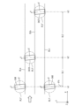
- Figure 2 is a diagram showing an example arrangement of the projection areas IAn of the DMD 10 projected onto the substrate P by the projection units PLU of each of the exposure modules MU(A), MU(B), and MU(C), with the Cartesian coordinate system XYZ set to the same as in Figure 1.
- the projection areas IAn can be said to be the irradiation range (light irradiation area group) of the illumination light reflected by the multiple micromirrors Ms of the DMD 10 and directed onto the substrate P by the projection unit PLU.
- the first row of exposure modules MU(A), the second row of exposure modules MU(B), and the third row of exposure modules MU(C), which are spaced apart in the X-axis direction, are each composed of nine modules aligned in the Y-axis direction.
- Exposure module MU(A) is made up of nine modules MU1 to MU9 arranged in the +Y direction
- exposure module MU(B) is made up of nine modules MU10 to MU18 arranged in the -Y direction
- exposure module MU(C) is made up of nine modules MU19 to MU27 arranged in the +Y direction.
- Modules MU1 to MU27 all have the same configuration, and when exposure module MU(A) and exposure module MU(B) are arranged facing each other in the X-axis direction, exposure module MU(B) and exposure module MU(C) are arranged back-to-back in the X-axis direction.
- the shape of the projection areas IA1, IA2, IA3, ..., IA27 (sometimes referred to as IAn, where n is 1 to 27) by each of the modules MU1 to MU27 is, as an example, a rectangle extending in the Y-axis direction with an aspect ratio of approximately 1:2.
- patchwork exposure is performed at the -Y direction ends of each of the projection areas IA1 to IA9 in the first row and the +Y direction ends of each of the projection areas IA10 to IA18 in the second row.
- the areas on the substrate P that are not exposed by each of the projection areas IA1 to IA18 in the first and second rows are patchwork exposed by each of the projection areas IA19 to IA27 in the third row.
- the center point of each of the projection areas IA1 to IA9 in the first row is located on a line k1 parallel to the Y axis
- the center point of each of the projection areas IA10 to IA18 in the second row is located on a line k2 parallel to the Y axis
- the center point of each of the projection areas IA19 to IA27 in the third row is located on a line k3 parallel to the Y axis.
- the distance between lines k1 and k2 in the X-axis direction is set to a distance XL1
- the distance between lines k2 and k3 in the X-axis direction is set to a distance XL2.
- the joint between the -Y end of projection area IA9 and the +Y end of projection area IA10 is OLa
- the joint between the -Y end of projection area IA10 and the +Y end of projection area IA27 is OLb
- the joint between the +Y end of projection area IA8 and the -Y end of projection area IA27 is OLc.
- the orthogonal coordinate system XYZ is set to be the same as in Figures 1 and 2, and the coordinate system X'Y' in projection areas IA8, IA9, IA10, IA27 (and all other projection areas IAn) is set to be inclined by an angle ⁇ k (0° ⁇ k ⁇ 90°) with respect to the X and Y axes (lines k1-k3) of the orthogonal coordinate system XYZ. That is, the area (light irradiation area) on the substrate P onto which the illumination light reflected by the numerous micromirrors of the DMD 10 is projected is arranged two-dimensionally along the X' axis and the Y' axis.
- the circular area encompassing each of the projection areas IA8, IA9, IA10, IA27 in FIG. 3 (and all other projection areas IAn as well) represents the circular image field PLf' of the projection unit PLU.
- the projected image (light irradiation area) of the micromirrors arranged diagonally (at an angle ⁇ k) at the -Y' end of the projection area IA9 is set to overlap with the projected image (light irradiation area) of the micromirrors arranged diagonally (at an angle ⁇ k) at the +Y' end of the projection area IA10.
- the projected image (light irradiation area) of the micromirrors arranged diagonally (at an angle ⁇ k) at the -Y' end of the projection area IA10 is set to overlap with the projected image (light irradiation area) of the micromirrors arranged diagonally (at an angle ⁇ k) at the +Y' end of the projection area IA27.
- the projected image (light irradiation area) of the micromirrors arranged diagonally (at an angle ⁇ k) at the end of the projection area IA8 in the +Y' direction is set to overlap with the projected image (light irradiation area) of the micromirrors arranged diagonally (at an angle ⁇ k) at the end of the projection area IA27 in the -Y' direction.
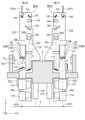
- FIG. 4 is an optical layout diagram showing the specific configuration of the module MU18 in the exposure module MU(B) shown in FIG. 1 and FIG. 2 and the module MU19 in the exposure module MU(C) as viewed in the XZ plane.
- the orthogonal coordinate system XYZ in FIG. 4 is set to be the same as the orthogonal coordinate system XYZ in FIG. 1 to FIG. 3.
- the module MU18 is shifted by a certain distance in the +Y direction with respect to the module MU19, and is installed back-to-back.
- the optical fiber unit FBU shown in FIG. 1 is composed of 27 optical fiber bundles FB1 to FB27 corresponding to each of the 27 modules MU1 to MU27 shown in FIG. 2.
- the illumination unit ILU of the module MU18 includes a mirror 100 that reflects the illumination light ILm traveling in the -Z direction from the output end of the optical fiber bundle FB18, a mirror 102 that reflects the illumination light ILm from the mirror 100 in the -Z direction, an input lens system 104 that acts as a collimator lens, an illuminance adjustment filter 106, an optical integrator 108 including a micro fly's eye (MFE) lens and a field lens, a condenser lens system 110, and an inclined mirror 112 that reflects the illumination light ILm from the condenser lens system 110 toward the DMD 10.
- the mirror 102, the input lens system 104, the optical integrator 108, the condenser lens system 110, and the inclined mirror 112 are arranged along an optical axis AXc that is parallel to the Z axis.
- the optical fiber bundle FB18 is composed of one optical fiber line or a bundle of multiple optical fiber lines.
- the illumination light ILm irradiated from the output end of the optical fiber bundle FB18 (each of the optical fiber lines) is set to a numerical aperture (NA, also called the spread angle) such that it enters the input lens system 104 in the subsequent stage without being vignetted.
- NA numerical aperture
- the illumination light ILm is light that has a peak wavelength within a wavelength range of 10 nm or more and 410 nm or less, and the peak wavelength is, for example, any of 193 nm, 248 nm, 365 nm (i-line), 405 nm (h-line), and 436 nm (g-line).
- the position of the front focal point of the input lens system 104 is designed to be the same as the position of the exit end of the optical fiber bundle FB18. Furthermore, the position of the rear focal point of the input lens system 104 is set so that the illumination light ILm from a single or multiple point light sources formed at the exit end of the optical fiber bundle FB18 is superimposed on the incident surface side of the MFE lens 108A of the optical integrator 108. Therefore, the incident surface of the MFE lens 108A is Koehler illuminated by the illumination light ILm from the exit end of the optical fiber bundle FB18.
- the geometric center point in the XY plane of the exit end of the optical fiber bundle FB18 is located on the optical axis AXc, and the main ray (center line) of the illumination light ILm from the point light source at the exit end of the optical fiber line is parallel (or coaxial) to the optical axis AXc.
- the illumination light ILm from the input lens system 104 is attenuated by an arbitrary value in the range of 0% to 90% by the illuminance adjustment filter 106, and then passes through the optical integrator 108 (MFE lens 108A, field lens, etc.) and enters the condenser lens system 110.
- the MFE lens 108A is a two-dimensional array of many rectangular microlenses with a side length of several tens of ⁇ m, and its overall shape is set to be approximately similar to the overall shape of the mirror surface of the DMD 10 (aspect ratio is approximately 1:2) in the XY plane.
- the position of the front focal point of the condenser lens system 110 is set to be approximately the same as the position of the exit surface of the MFE lens 108A. Therefore, each of the illumination lights from the point light sources formed on the exit side of each of the many microlenses of the MFE lens 108A is converted into an approximately parallel light beam by the condenser lens system 110, reflected by the inclined mirror 112, and then superimposed on the DMD 10 to form a uniform illuminance distribution.
- the exit surface of the MFE lens 108A generates a surface light source in which many point light sources (light focusing points) are densely arranged in a two-dimensional manner, so it functions as a surface light source component.
- optical axis AXc which is parallel to the Z axis and passes through condenser lens system 110, is bent by tilted mirror 112 to reach DMD 10, and the optical axis between tilted mirror 112 and DMD 10 is optical axis AXb.
- the neutral plane including the center points of each of the numerous micromirrors of DMD 10 is set parallel to the XY plane. Therefore, the angle between the normal to that neutral plane (parallel to the Z axis) and optical axis AXb is the angle of incidence ⁇ of illumination light ILm with respect to DMD 10.
- Fig. 5(A) is a diagram showing a schematic of the DMD 10
- Fig. 5(B) is a diagram showing the DMD 10 when the power is OFF
- Fig. 5(C) is a diagram for explaining the mirror in the ON state
- Fig. 5(D) is a diagram for explaining the mirror in the OFF state. Note that in Figs. 5(A) to 5(D), mirrors in the ON state are shown by hatching.
- the DMD 10 has multiple micromirrors Ms whose reflection angles can be changed.
- the DMD 10 uses a roll and pitch drive system that switches between the ON and OFF states by tilting the micromirrors Ms in the roll and pitch directions.
- each micromirror Ms when the power is OFF (micromirror Ms is in a neutral state), the reflective surface of each micromirror Ms is set parallel to the X'Y' plane.
- Each micromirror Ms is turned ON by tilting around the Y' axis.
- FIG. 5C shows a case where only the central micromirror Ms is turned ON, and the other micromirrors Ms are in a neutral state (neither ON nor OFF).
- Each micromirror Ms is turned OFF by tilting around the X' axis.
- FIG. 5D shows a case where only the central micromirror Ms is turned OFF, and the other micromirrors Ms are in a neutral state.
- the micromirror Ms in the ON state is driven to tilt at a predetermined angle from the X'Y' plane so that the illumination light irradiated to the micromirror Ms in the ON state is reflected in the X-axis direction of the XZ plane.
- the micromirror Ms in the OFF state is driven to tilt at a predetermined angle from the X'Y' plane so that the illumination light irradiated to the micromirror Ms in the OFF state is reflected in the Y-axis direction in the YZ plane.
- the DMD 10 generates an exposure pattern by switching the ON and OFF states of each micromirror Ms.
- the illumination light reflected by the mirror in the OFF state is absorbed by a light absorber (not shown).
- the DMD 10 has been described as an example of a spatial light modulator, and therefore as a reflective type that reflects laser light, but the spatial light modulator may be a transmissive type that transmits laser light, or a diffractive type that diffracts laser light.
- the spatial light modulator can modulate the laser light spatially and temporally.
- illumination light ILm irradiated to micromirrors Ms of the DMD 10 that are in the ON state is reflected in the X-axis direction in the XZ plane so as to head toward the projection unit PLU.
- illumination light ILm irradiated to micromirrors Ms of the DMD 10 that are in the OFF state is reflected in the Y-axis direction in the YZ plane so as not to head toward the projection unit PLU.
- a movable shutter 114 is removably provided in the optical path between the DMD 10 and the projection unit PLU to block reflected light from the DMD 10 during non-exposure periods. As shown on the module MU19 side, the movable shutter 114 is rotated to an angular position where it is removed from the optical path during exposure periods, and is rotated to an angular position where it is inserted obliquely into the optical path during non-exposure periods, as shown on the module MU18 side. A reflective surface is formed on the DMD 10 side of the movable shutter 114, and the light from the DMD 10 reflected there is irradiated onto the light absorber 115.
- the light absorber 115 absorbs light energy in the ultraviolet wavelength range (wavelengths of 400 nm or less) without re-reflecting it and converts it into heat energy. For this reason, the light absorber 115 is also provided with a heat dissipation mechanism (heat dissipation fins and a cooling mechanism). Although not shown in FIG. 4, the reflected light from the micromirror Ms of the DMD 10, which is in the OFF state during the exposure period, is absorbed by a similar light absorber (not shown in FIG. 4) installed in the Y-axis direction (direction perpendicular to the paper surface of FIG. 4) with respect to the optical path between the DMD 10 and the projection unit PLU, as described above.
- a similar light absorber not shown in FIG. 4 installed in the Y-axis direction (direction perpendicular to the paper surface of FIG. 4) with respect to the optical path between the DMD 10 and the projection unit PLU, as described above.
- the DMD 10 is used in the form of a package (chip).
- Fig. 6(A) is a perspective view showing an example of a DMD chip CHP including the DMD 10
- Fig. 6(B) is a diagram showing an example of an X'Z' cross section of the DMD chip CHP.
- the direction perpendicular to the neutral plane of the DMD 10 is the Z'-axis direction.
- the DMD chip CHP includes the DMD 10, a frame body FRM that surrounds the DMD 10, and a substrate SB on which the DMD 10 and frame body FRM are mounted.
- the frame body FRM is supported by a support part SPP.
- the support part SPP is made of metal, glass material, resin, or the like.
- the frame body FRM and the support part SPP may be integral.
- the frame body FRM has an opening OPN11.
- the DMD10 overlaps with the opening OPN11 of the frame body FRM.
- the reflectance of the frame body FRM to the illumination light ILm is greater than the reflectance of the multiple micromirrors Ms to the illumination light ILm.
- the DMD chip CHP also includes a cover glass CGLS that protects the DMD 10.
- the cover glass CGLS is supported by the frame body FRM.
- the cover glass CGLS is not limited to glass and may be, for example, quartz, as long as it is a transparent member that transmits the illumination light ILm.
- the cover glass CGLS may be omitted.
- the DMD chip CHP is attached to a fine movement stage 10S provided on a mount 10M fixed to a support column of the illumination unit ILU.
- a fine movement stage 10S for example, a fine movement stage combining a parallel link mechanism and an expandable piezoelectric element as disclosed in International Patent Publication No. 2006/120927 can be used. This allows fine adjustment of the position and attitude of the DMD 10.
- the area on the X'Y' plane illuminated by illumination light ILm at the position of the neutral plane of DMD 10 is called the illumination field area.
- the illumination field area is set so that the entire DMD 10 is illuminated by illumination light ILm even if the position of DMD 10 is shifted in the X'-axis direction, Y'-axis direction, or ⁇ z direction by fine movement stage 10S.
- the illumination field area is an area that is the dimension of DMD 10 plus the movable range of DMD 10 in the X'-axis direction and Y'-axis direction, and the size of the illumination field area is larger than the size of DMD 10.
- the illumination light ILm illuminates DMD 10 and the periphery of DMD 10.
- part of the illumination light ILm may enter the frame body FRM of the DMD chip CHP and be reflected by the frame body FRM, causing scattered light (flare light) and becoming stray light.
- scattered light freo light
- stray light The occurrence of stray light has a negative effect on the exposure results.
- a light-shielding cover CVR is provided that limits the incidence of illumination light ILm on the frame body FRM (see FIG. 4).
- the DMD chip CHP and the light-shielding cover CVR may be collectively referred to as the spatial light modulation unit SLMU.
- the light-shielding cover CVR is located on the side of the DMD chip CHP where the illumination light ILm is incident on the DMD 10.
- the light-shielding cover CVR is also attached to the DMD chip CHP. It is preferable that the light-shielding cover CVR is positioned away from the frame FRM and the cover glass CGLS. By positioning it in this way, the light-shielding cover CVR can be separated from the DMD 10, and the effect of heat absorbed by the light-shielding cover CVR on the DMD 10 can be suppressed.
- the reflectance of the light shielding cover CVR to the illumination light ILm is smaller than the reflectance of the multiple micromirrors Ms to the illumination light ILm. More specifically, the light shielding cover CVR is subjected to low-reflection treatment (black chrome plating, etc.) so that the reflectance of the illumination light ILm is 20% or less, preferably about 10% or less. This makes it possible to suppress the generation of scattered light due to the illumination light ILm being reflected by the light shielding cover CVR.
- the entire light shielding cover CVR may be subjected to low-reflection treatment, but it is sufficient that at least the surface of the light shielding cover CVR on which the illumination light ILm is incident (the surface on the -Z side) is subjected to low-reflection treatment.
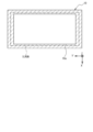
- Figure 7(A) is a view of the DMD chip CHP without the light-shielding cover CVR attached, viewed from the -Z direction
- Figure 7(B) is a view of the DMD chip CHP with the light-shielding cover CVR attached, viewed from the -Z direction.
- Figure 7(B) the components of the DMD chip CHP hidden by the light-shielding cover CVR are shown with dotted lines.
- an opening OPN1 is formed in the light-shielding cover CVR (the light-shielding cover CVR has an opening OPN1).
- the illumination light ILm is incident on the DMD 10 through the opening OPN1.
- the opening OPN1 of the light-shielding cover CVR overlaps with the frame body FRM.
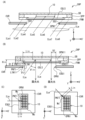
- Figure 8(A) is a cross-sectional view for explaining the arrangement of the DMD chip CHP and the light-shielding cover CVR
- Figure 8(B) is a cross-sectional view for explaining the size of the opening OPN1 of the DMD chip CHP and the positional relationship between the DMD chip CHP and the opening OPN1.
- Figures 8(A) and 8(B) illustrate the case where illumination light ILm is incident on the DMD 10 from a direction parallel to the X' axis.
- the portion of the light-shielding cover CVR other than the opening OPN1 overlaps with the frame body FRM of the DMD chip CHP.
- the illumination light ILm1, illumination light ILm2, illumination light ILm7, and illumination light ILm8 that would be incident on the frame body FRM if the light-shielding cover CVR was not installed is prevented from entering the frame body FRM by the light-shielding cover CVR. This prevents the illumination light ILm1, illumination light ILm2, illumination light ILm7, and illumination light ILm8 from being reflected by the frame body FRM and causing scattered light.
- the portions of the light-shielding cover CVR other than the opening OPN1 do not overlap with the DMD10 when viewed from the direction in which the illumination light ILm is incident. This allows illumination light ILm4 to illumination light ILm6 to be incident on the DMD10.
- the distance between the +Z side surface of the light-shielding cover CVR and a plane that includes the point closest to the substrate SB on the reflective surface of the micromirror Ms and is parallel to the surface of the substrate SB, or a plane that includes the reflective surface of the micromirror Ms when the reflective surface of the micromirror Ms of the DMD 10 is parallel to the surface of the substrate SB, is Hin
- the distance between the -Z side surface of the frame FRM and the +Z side surface of the light-shielding cover CVR is D1, then Hin > D1.
- ⁇ in is twice the inclination angle of the reflecting surface of the micromirror Ms when the micromirror Ms is in the ON state.
- ⁇ in may be set taking into consideration the error (e.g., ⁇ 0.5°) of the inclination angle of the reflecting surface of the micromirror Ms when the micromirror Ms is in the ON state.
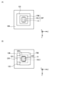
- Figures 8(C) and 8(D) are views of the DMD 10 and the opening OPN1 from the -Z direction.
- the illumination light ILm is incident on the DMD 10 from a direction parallel to the X' axis.
- the point where the edge EDG1 forming the opening OPN1 intersects with the line indicating the optical axis of the incident light ILm is the point PNT1.
- the micromirror Ms closest to PNT1 is shown hatched.
- the illumination light ILm enters the DMD 10 from a direction tilted with respect to the X' axis (or Y' axis).
- the point where the edge EDG1 that forms the opening OPN1 intersects with the line indicating the optical axis of the incident light ILm is the point PNT1.
- the micromirror Ms closest to PNT1 is shown hatched.
- the illumination light ILm is not blocked from entering the DMD 10, and the illumination light ILm is prevented from reflecting off the frame FRM and causing scattered light. This makes it possible to prevent stray light from occurring.
- PNT11 is a point on the edge EDG11 that forms the opening OPN11 of the frame body FRM of the DMD chip CHP, which is in a plane perpendicular to the surface of the substrate SB and includes a line connecting point PNT1 on the edge EDG1 of the opening OPN1 of the light-shielding cover CVR and the micromirror Ms closest to point PNT1.
- the inclination angle ⁇ c of the line LIN11 connecting point PNT11 and point PNT1 with respect to the line LIN1 perpendicular to the surface of the substrate SB is smaller than ⁇ in. This allows the illumination light ILm to be prevented from entering the DMD10, and also prevents the illumination light ILm from being reflected by the frame body FRM and causing scattered light.
- the distance Lin in the X'-axis direction between the side SD1 on the side where the illumination light ILm is incident and the DMD 10 is longer than the distance D2 in the X'-axis direction between the other side SD2 and the DMD 10 (see FIG. 8B). This makes it possible to prevent the illumination light ILm that is obliquely incident on the DMD 10 from being vignetted by the light-shielding cover CVR.
- the opening OPN1 of the light-shielding cover CVR also passes illumination light (hereinafter referred to as discarded light) ILm_out reflected by the micromirror Ms in the OFF state.
- Figure 9 is a diagram explaining the arrangement of the opening OPN1 and the DMD 10, and the relationship with the discarded light ILm_out. In Figure 9, the discarded light ILm_out travels in the Y'-axis direction.
- Hout is the distance between the surface of the light-shielding cover CVR and a plane that includes the closest point to the substrate SB on the reflective surface of the micromirror Ms when the micromirror Ms of the DMD 10 is in the OFF state and is parallel to the surface of the substrate SB, or a plane that includes the reflective surface of the micromirror Ms when the reflective surface of the micromirror Ms of the DMD 10 is parallel to the surface of the substrate SB.
- the angle that is formed between the optical axis AXex of the exposure light and the optical axis of the waste light ILm_out is ⁇ out. Also, the distance between the point PNT3 where the plane (X'Y' plane in FIG.
- the direction in which the waste light ILm_out reflected by the micromirror Ms in the OFF state travels is not limited to the Y'-axis direction, but depends on the setting of the DMD 10. Even if the direction of travel of the waste light ILm_out is not the Y'-axis direction, ⁇ out is the angle between the optical axis AXex of the exposure light and the optical axis of the waste light ILm_out, and Lout is the distance between the point where a plane perpendicular to the surface of the substrate SB, which includes the optical axis AXex of the exposure light and the optical axis of the waste light ILm_out, intersects with the edge EDG1 that forms the opening OPN1, and the micromirror Ms that is closest to that point among the multiple micromirrors Ms of the DMD 10, as long as tan ⁇ out ⁇ Lout/Hout is satisfied.
- the light-shielding cover CVR may be attached to a member other than the DMD chip CHP.
- the light-shielding cover CVR is fixed so that the relative positional relationship between the opening OPN1 and the DMD 10 does not change.
- the light-shielding cover CVR may be fixed to the fine movement stage 10S.
- the light-shielding cover CVR may be fixed to a member other than the DMD chip CHP or the fine movement stage 10S, and in this case, the light-shielding cover CVR may be shifted in accordance with the shift in position of the DMD 10 by the fine movement stage 10S.
- the projection unit PLU attached to the underside of the optical base 5 is configured as a double-telecentric imaging projection lens system composed of a first lens group 116 and a second lens group 118 arranged along an optical axis AXa parallel to the Z axis.
- the first lens group 116 and the second lens group 118 are each configured to translate in a direction along the Z axis (optical axis AXa) by a micro-movement actuator relative to a support column fixed to the underside of the optical base 5.
- the projection magnification Mp is set to approximately 1/6, taking into consideration the tilt angle ⁇ k in the XY plane of the projection area IAn (DMD10) described above in FIG. 3.
- the imaging projection lens system consisting of lens groups 116 and 118 inverts/flips a reduced image of the entire mirror surface of DMD10 and images it on the projection area IA18 (IAn) on the substrate P.
- the first lens group 116 of the projection unit PLU can be moved slightly in the direction of the optical axis AXa by an actuator to fine-tune the projection magnification Mp (approximately ⁇ several tens of ppm), and the second lens group 118 can be moved slightly in the direction of the optical axis AXa by an actuator to quickly adjust the focus. Furthermore, in order to measure the positional change in the Z-axis direction of the surface of the substrate P with an accuracy of submicron or less, multiple focus sensors 120 of the oblique incidence type are provided below the optical table 5.
- the illumination unit ILU and projection unit PLU require the projection area IAn to be tilted by an angle ⁇ k in the XY plane, so the DMD 10 and illumination unit ILU in Figure 4 (at least the optical path portion from mirror 102 to mirror 112 along the optical axis AXc) are positioned so that they are tilted overall by an angle ⁇ k in the XY plane.
- FIG. 10 is a schematic diagram showing the state in which the DMD 10 and projection unit PLU are tilted by an angle ⁇ k in the XY plane.
- the orthogonal coordinate system XYZ is the same as the coordinate systems XYZ in FIGS. 1 to 4
- the array coordinate system X'Y' of the micromirrors Ms of the DMD 10 is the same as the coordinate system X'Y' shown in FIG. 3.
- the circle containing the DMD 10 is the image field PLf on the object side of the projection unit PLU, and the optical axis AXa is located at its center.
- the optical axis AXc that passes through the condenser lens system 110 of the illumination unit ILU is bent by the tilted mirror 112 to form an optical axis AXb, which is positioned so that it is tilted by an angle ⁇ k from a line Lu parallel to the X-axis when viewed in the XY plane.
- the light beam (i.e., the spatially modulated light beam) formed only by the reflected light from the micromirrors Ms of the DMD 10 that are in the ON state is irradiated via the projection unit PLU onto an area on the substrate P that is optically conjugate with the micromirrors Ms.
- the pattern generated by the DMD 10 is formed on the substrate P.
- the spatial light modulation unit SLMU comprises a DMD 10 having a plurality of micromirrors Ms arranged two-dimensionally, a DMD chip CHP including a frame body FRM surrounding the DMD 10 and a substrate SB on which the DMD 10 and frame body FRM are mounted, and a light-shielding cover CVR located on the side of the DMD chip CHP where the illumination light ILm enters the DMD 10 and attached to the DMD chip CHP, which limits the incidence of the illumination light ILm on the frame body FRM, the light-shielding cover CVR having an opening OPN1, through which the illumination light ILm enters the DMD 10. This causes the illumination light ILm to be reflected by the frame body FRM, generating scattered light, and thus making it possible to suppress the generation of stray light.
- the opening OPN1 of the light-shielding cover CVR overlaps with the frame body FRM. This prevents the illumination light ILm that should be incident on the DMD 10 from being vignetted by the light-shielding cover CVR.
- the distance Hin between the light-shielding cover CVR and the DMD 10 is greater than the distance D1 between the light-shielding cover CVR and the frame body FRM. This makes it possible to prevent the illumination light ILm that should be incident on the DMD 10 from being vignetted by the light-shielding cover CVR.
- the distance Hin between the light-shielding cover CVR and the DMD 10 may be equal to the distance D1 between the light-shielding cover CVR and the frame body FRM.
- the exposure apparatus EX includes a spatial light modulation unit SLMU, an illumination unit ILU that illuminates the DMD chip CHP with illumination light ILm, and a fine movement stage 10S that carries the DMD chip CHP and moves within a plane parallel to the surface of the substrate SB. This allows the position of the DMD 10 to be shifted.
- the illumination unit ILU illuminates the DMD 10 and the area around the DMD 10. This makes it possible to prevent areas of the DMD 10 that are not illuminated by the illumination light ILm from occurring, even if the position of the DMD 10 shifts.
- the exposure apparatus EX is equipped with a DMD chip CHP including a DMD 10 having a plurality of micromirrors Ms arranged two-dimensionally and a frame body FRM surrounding the DMD 10, an illumination unit ILU that illuminates the DMD chip CHP with illumination light ILm, a light-shielding cover CVR that blocks the illumination light ILm from entering the frame body FRM, and a projection unit PLU that projects the light from the DMD 10 onto a substrate P that is scanned in the scanning direction. Since the light-shielding cover CVR blocks the illumination light ILm from entering the frame body FRM, it is possible to suppress the occurrence of stray light caused by the illumination light ILm being reflected by the frame body FRM and the generation of scattered light.
- the light-shielding cover CVR is formed with a substantially rectangular opening OPN1 that allows the illumination light ILm to pass through, and when viewed from the direction in which the illumination light ILm is incident on the DMD chip CHP, the portion of the light-shielding cover CVR other than the opening OPN1 overlaps with the frame body FRM of the DMD chip CHP. This causes the illumination light ILm to be reflected by the frame body FRM, generating scattered light, which can prevent the generation of stray light.
- the light-shielding cover CVR overlaps with the frame body FRM when viewed from the incidence direction of the illumination light ILm so that the illumination light ILm does not enter the frame body FRM of the DMD chip CHP, but this is not limited to this.
- the light-shielding cover CVR may be omitted, and the frame body FRM may be subjected to a low-reflection treatment (black chrome plating, etc.) so that the reflectance of the illumination light ILm is 20% or less, preferably 10% or less. Even in this way, it is possible to prevent the illumination light ILm from being reflected by the frame body FRM and the generation of scattered light (flare light).
- the light-shielding cover CVR may be provided. The effect of heat on the DMD 10 can be suppressed.
- the size of the opening OPN1 of the light-shielding cover CVR on the DMD 10 side was approximately the same as the size of the opening OPN1 on the opposite side to the DMD 10 (the inner wall of the opening OPN1 of the light-shielding cover CVR was approximately perpendicular to the neutral plane (X'Y' plane) of the DMD 10), but this is not limited to this.
- the size of the opening OPN1 on the opposite side to the DMD 10 may be larger than the size of the opening OPN1 on the DMD 10 side.
- the inner wall of the opening OPN1 may be inclined. This makes it possible to prevent the illumination light ILm that should be incident on the DMD 10 from being vignetted by the light-shielding cover CVR.
- the light-shielding cover CVR is intended to prevent the illumination light ILm from entering the frame body FRM of the DMD chip CHP, but this is not limited to the above.
- the light-shielding cover may be arranged to prevent the scattered light (flare light) generated by the reflection of the illumination light ILm by the frame body FRM from proceeding to the substrate P.
- the light-shielding cover may be arranged in a position that prevents the progression of the scattered light but does not prevent the progression of the exposure light reflected by the micromirror Ms in the ON state.
- FIG. 12 is a diagram to explain the light-shielding cover CVR3 that blocks the progression of scattered light.
- scattered light is shown by a dashed line
- exposure light is shown by a solid line.
- the light-shielding cover CVR3 has an opening OPN4 that passes light (exposure light) reflected by the micromirror Ms in the ON state.
- the size of the opening OPN4 of the light-shielding cover CVR3 and the positional relationship between the DMD 10 and the light-shielding cover CVR3 are determined so as to block the progression of scattered light but not block the progression of exposure light reflected by the micromirror Ms in the ON state.
- the size of the opening OPN4 and the positional relationship between the light-shielding cover CVR3 and the DMD 10 are determined so as to satisfy tan ⁇ NA ⁇ L/H.
- L is the distance between the opening OPN4 of the light-shielding cover CVR3 and the DMD 10
- H is the distance between the plane including the reflection surface of the micromirror Ms when the reflection surface of the micromirror Ms provided in the DMD 10 is parallel to the surface of the substrate SB and the +Z side surface of the light-shielding cover CVR3.
- NA indicates the numerical aperture of the projection unit PLU
- n indicates the refractive index of the optical path medium
- ⁇ indicates the optical magnification.
- a light-shielding cover CVR3 may be provided that blocks the scattered light (flare light) generated by the reflection of the illumination light ILm by the frame FRM from proceeding to the substrate P.
- Second Embodiment 13 is an optical layout diagram showing a specific configuration of the module MU18 in the exposure module MU(B) and the module MU19 in the exposure module MU(C) in the second embodiment, viewed in the XZ plane.
- the area on the substrate P conjugate with each micromirror Ms is called a light irradiation area, and a collection of light irradiation areas is called a light irradiation area group.
- the projection area IAn coincides with the light irradiation area group.
- the light irradiation area group on the substrate P has a large number of light irradiation areas arranged in two-dimensional directions (X'-axis direction and Y'-axis direction).
- the second embodiment differs from the first embodiment in that a field stop FS is disposed in the optical path of the illumination light ILm between the optical integrator 108 and the DMD 10.
- FIG. 14 The imaging state of the micromirror Ms of the DMD 10 by the projection unit PLU (imaging projection lens system) will be described in detail with reference to Fig. 14.
- the Cartesian coordinate system X'Y'Z in Fig. 14 is the same as the coordinate system X'Y'Z shown in Figs. 3 and 10, and Fig. 14 illustrates the optical path from the condenser lens system 110 of the illumination unit ILU to the substrate P.
- Illumination light ILm from the condenser lens system 110 travels along the optical axis AXc, is totally reflected by the tilted mirror 112, and reaches the mirror surface of the DMD 10 along the optical axis AXb.
- micromirror Ms located at the center of the DMD 10 is designated Msc
- micromirrors Ms located on the periphery are designated Msa
- these micromirrors Msc and Msa are assumed to be in the ON state.
- the angle of incidence ⁇ (angle of optical axis AXb from optical axis AXa) of the illumination light ILm irradiated to the DMD 10 is set to 35.0° in order to make the chief rays of the reflected light Sc and Sa from each of the micromirrors Msc and Msa parallel to the optical axis AXa of the projection unit PLU.
- the chief ray Lc of the reflected light Sc from the micromirror Msc is coaxial with the optical axis AXa
- the chief ray La of the reflected light Sa from the micromirror Msa is parallel to the optical axis AXa
- the reflected light Sc and Sa enter the projection unit PLU with a predetermined numerical aperture (NA).
- a reduced image ic of the micromirror Msc reduced by the projection magnification Mp of the projection unit PLU is formed on the substrate P in a telecentric state at the position of the optical axis AXa.
- a reduced image ia of the micromirror Msa reduced by the projection magnification Mp of the projection unit PLU is formed on the substrate P in a telecentric state at a position away from the reduced image ic in the +X' direction.
- the first lens group 116 of the projection unit PLU is composed of two lens groups G1 and G2
- the second lens group 118 is composed of three lens groups G3, G4, and G5.
- An exit pupil (also simply called a pupil) Ep is set between the lens group G3 and the lens group G4 of the second lens group 118.
- a light source image of the illumination light ILm (a collection of many point light sources formed on the exit surface side of the MFE lens 108A) is formed, forming a Koehler illumination configuration.
- the pupil Ep is also called the aperture of the projection unit PLU, and the size (diameter) of that aperture is one of the factors that determine the resolution of the projection unit PLU.
- the illumination light ILm irradiated onto the entire mirror surface of the DMD 10 has a uniform illuminance distribution (for example, intensity unevenness within ⁇ 1%) due to the action of the optical integrator 108.
- the exit end side of the MFE lens 108A and the surface of the pupil Ep of the projection unit PLU are set in an optically conjugate relationship by the condenser lens system 110 and the lens groups G1 to G3 of the projection unit PLU.
- FIG. 15A is a diagram showing a schematic diagram of a projection area (light irradiation area group) IAn and exposure target areas (areas to which a line pattern is exposed) 30a, 30b on a substrate P.
- the exposure target areas 30a, 30b are scanned with respect to the projection area (light irradiation area group) IAn, and the DMD 10 turns on the micromirror Ms corresponding to the light irradiation area 32 at the timing when the center (called the spot position) of the light irradiation area 32 included in the projection area (light irradiation area group) IAn is located within the exposure target areas 30a, 30b.
- rectangular area 34a which is part of line-shaped exposure target area 30a
- rectangular area 34b which is part of exposure target area 30b (see dashed lines (symbols 34a, 34b) in FIG. 15(A)).
- These rectangular areas 34a, 34b are, for example, square areas with sides measuring 1 ⁇ m.
- the light irradiation area 32 corresponding to each micromirror Ms is also a square area with sides measuring 1 ⁇ m.
- FIG. 15(B) shows the state in which rectangular areas 34a and 34b are exposed with 61 pulses and 61 spot positions arranged (staggered arrangement).
- manufacturing errors of each component, assembly errors, and variations in the optical characteristics of the optical components may cause a difference (illuminance unevenness) between the integrated illuminance (total amount of exposure) of rectangular area 34a and the integrated illuminance of rectangular area 34b.
- the integrated illuminance may differ depending on the position in the Y-axis direction, resulting in an uneven distribution of integrated illuminance in the Y-axis direction. It is desirable for the integrated illuminance distribution in the Y-axis direction to be uniform.
- the integrated illuminance of rectangular area 34a is higher than the integrated illuminance of rectangular area 34b, it is conceivable to reduce the amount of exposure to rectangular area 34a and correct (reduce) the integrated illuminance of rectangular area 34a by turning off some of the micromirrors Ms that are to be turned on when exposing rectangular area 34a.
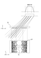
- a field stop FS is disposed on the optical path of the illumination light ILm between the optical integrator 108 and the DMD 10.
- Fig. 16(A) is a plan view of the field stop FS
- Fig. 16(B) is a cross-sectional view along line A-A in Fig. 16(A).
- Fig. 17(A) is a diagram for explaining the arrangement of the field stop FS
- Fig. 17(B) is a diagram showing the illuminance distribution of the illumination light formed by the field stop FS.
- the field stop FS has a first member 40a and a second member 40b.
- the first member 40a is a quadrangular prism with a substantially rectangular cross section
- the second member 40b is a quadrangular prism with a substantially right-angled trapezoidal cross section.
- the side surface 41b (see FIG. 17(B)) of the second member 40b facing the illumination light ILm is inclined with respect to the bottom surface so that the angle (interior angle) between the bottom surface and the side surface 41b is an acute angle. This prevents the illumination light ILm from being reflected by the side surface 41b facing the illumination light ILm of the field stop FS.
- the field stop FS is subjected to a low-reflection treatment (black chrome plating, etc.) so that the reflectance of the illumination light ILm is 20% or less, preferably approximately 10% or less. This prevents the illumination light ILm from being reflected by the field stop FS, generating scattered light and thus stray light.
- the field stop FS is disposed between the tilted mirror 112 and the DMD 10.
- the field stop FS may be disposed at any position on the optical path of the illumination light ILm between the optical integrator 108 and the DMD 10.
- the field stop FS may be disposed between the condenser lens system 110 and the tilted mirror 112, or between the optical integrator 108 and the condenser lens system 110.
- the field stop FS is attached, for example, to the DMD chip CHP so that its relative positional relationship with the DMD 10 does not change.
- the field stop FS may also be attached, for example, to the fine movement stage 10S.
- the field stop FS may be fixed to a member other than the DMD chip CHP or the fine movement stage 10S, and in this case, the field stop FS may be shifted in accordance with the shift in position of the DMD 10 by the fine movement stage 10S.
- the first member 40a and the second member 40b extend in a direction (Y'-axis direction) that is approximately perpendicular to the scanning direction (X-axis direction) of the substrate P, of the two axial directions (X'-axis direction, Y'-axis direction) that define the array coordinate system X'Y' of the micromirror Ms.
- the first member 40a and the second member 40b block a portion of the illumination light ILm along the Y'-axis direction. This makes it possible to change the illuminance of the illumination light ILm depending on the position in the X'-axis direction.
- the first member 40a and the second member 40b are arranged at a predetermined interval in the X'-axis direction perpendicular to the Y'-axis direction, and block a part of the illumination light ILm along both ends of the X'-axis direction of the DMD 10.
- the illuminance distribution of the illumination light ILm in the X'-axis direction is an illuminance distribution in which the illuminance is low at both ends of the X'-axis direction of the DMD 10 and high in the center (a top-hat illuminance distribution shown in FIG. 17B).
- the illuminance distribution includes an area of illuminance greater than 0% and less than 50% of the maximum illuminance in the illuminance distribution.
- the illuminance distribution may include an area of illuminance greater than 0% and less than 100% of the maximum illuminance in the illuminance distribution, an area of illuminance greater than 10% and less than 90% of the maximum illuminance in the illuminance distribution, or an area of illuminance greater than 50% and less than 90% of the maximum illuminance in the illuminance distribution.
- first member 40a and the second member 40b are arranged so that their bottom surfaces are parallel to the neutral plane of the DMD 10. This makes it possible to make the effects of telecentricity symmetrical about the center.
- FIG. 18(A) shows an example of the illuminance distribution of illumination light ILm
- FIG. 18(B) shows an example of exposing a rectangular area 34 using illumination light ILm having the illuminance distribution shown in FIG. 18(A).
- spot position 342 is a spot position in the light irradiation area 32 onto which illumination light with 90% illuminance is projected.
- Spot position 343 is a spot position in the light irradiation area 32 onto which illumination light with 70% illuminance is projected, and spot position 344 is a spot position in the light irradiation area 32 onto which illumination light with 50% illuminance is projected.
- Spot position 345 is a spot position in the light irradiation area 32 onto which illumination light with 30% illuminance is projected.
- Spot position 341 is a spot position in the light irradiation area 32 other than spot positions 342 to 345 onto which illumination light with 100% illuminance is projected.
- the number of spot positions 342, 343, 344, and 345 is one each, and the number of spot positions 341 is 57.
- FIG. 19(A) is a diagram explaining how rectangular regions 34d-34f are exposed.
- the DMD 10 turns on the micromirror Ms corresponding to light irradiation regions 210a-210c when rectangular regions 34d-34f are at positions 34D-34F, respectively, and turns on the micromirror Ms corresponding to light irradiation regions 210d-210f when rectangular regions 34d-34f are at positions 34G-34I, respectively.
- rectangular regions 34d-34f move by the free running distance between pulses.
- Figure 19(B) is a diagram explaining how rectangular areas 34d to 34f are exposed when the integrated illuminance is corrected.
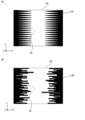
- the micromirrors Ms not used for exposure in this way are continuous in the scanning direction for a distance equivalent to the free running distance, so these micromirrors Ms are set to the OFF state.
- FIG. 19(B) the light irradiation area corresponding to the micromirrors Ms that are set to the OFF state is shown by hatching.
- the micromirrors Ms are also set to the OFF state continuously in the Y-axis direction.
- the micromirrors Ms that are turned OFF are continuous in the X'-axis and Y'-axis directions and form an approximately band-shaped range with a width in the scanning direction.
- each square represents a micromirror Ms
- the black squares represent micromirrors Ms that are in the OFF state.
- the spot interval (also called a grid) is 1/10 of the rectangular area 34d (also called a pixel), and the ON and OFF states must be determined for each spot (for each micromirror Ms).
- the ON and OFF states of the micromirror Ms may be determined for each pixel size, or the ON and OFF states of the micromirror Ms may be determined for each larger size (area including multiple pixels), and illuminance measurement may be performed in pixel units (rectangular area units).
- illuminance correction with a resolution of 0.1% is possible, so if there is an overall unevenness of about 2% in the illuminance uniformity, the area for applying the illuminance distribution should be of that size (about 1/20 of the length of the DMD 10).
- Fig. 21 is a view of the substrate holder 4B as seen from the +Z direction.
- the measurement unit IU is provided on the opposite side of the substrate holder 4B from the calibration reference unit CU in the X-axis direction. Note that the measurement unit IU may be provided on the same side as the calibration reference unit CU.
- multiple measurement devices 400a-400i are arranged in a direction (Y-axis direction) perpendicular to the scanning exposure direction (X-axis direction) of the substrate P.
- the measurement devices 400a-400i measure the illuminance of each micromirror Ms of the DMD 10 of the modules MU1-MU27.
- the multiple measurement devices 400a-400i can be arranged on the substrate holder 4B as shown in FIG. 21, but may also be arranged on the XY stage 4A or within the projection unit PLU.
- the measuring devices 400a to 400i are provided to correspond to, for example, the modules MU1 to MU9 of the exposure module group MU(A). That is, they are arranged so that the pitch P1 between the centers of adjacent modules in the Y-axis direction is equal to the pitch P2 between the centers of adjacent measuring devices in the Y-axis direction.
- the measuring devices 400a to 400i will be referred to as measuring devices 400.
- the measuring devices 400 may be provided to correspond to the modules MU1 to MU27. That is, 27 measuring devices 400 may be arranged in the measuring unit IU.
- the number of measuring devices 400 is not limited to the number shown in FIG. 21, and may be 8 or less, or 10 or more.
- the XY stage 4A can be stepped to measure the illuminance of each micromirror Ms of the DMD 10 of the modules MU1 to MU27, so the number of measuring devices 400 can be further reduced.
- the measurement device 400 is tilted in the XY plane by the angle ( ⁇ k: see FIG. 10) that the DMD 10 is tilted in the XY plane. Note that the measurement device 400 does not have to be positioned at an angle in the XY plane.
- the measuring device 400 includes, for example, a photosensor 402. For example, when one of the micromirrors Ms of the DMD 10 is turned ON and the other micromirrors Ms are turned OFF, the measuring device 400 measures and stores the illuminance (power) of the pattern image (exposure light) projected by the micromirror Ms that is turned ON, and repeats this process for the number of micromirrors Ms. This provides measurement results that associate each micromirror with the illuminance of the exposure light.
- An aperture plate that limits the measurement point such as a pinhole, may also be provided on the conjugate surface with the DMD 10.
- the measuring device 400 may include, for example, an image sensor (CCD or CMOS) having pixels corresponding to each micromirror Ms of the DMD 10. In this case, all the micromirrors Ms are turned on, and the illuminance of the pattern image projected by the corresponding micromirror Ms is measured at each pixel.
- CCD image sensor
- CMOS complementary metal-oxide-semiconductor
- the measuring device 400 may also include, for example, an imaging element having a number of pixels that is less than the number of micromirrors Ms provided in the DMD 10.
- multiple micromirrors Ms correspond to one pixel of the imaging element.
- the illuminance of the pattern image projected by the collection of multiple micromirrors Ms is measured at each pixel.
- the integrated illuminance at each position in the Y-axis direction can be calculated based on the measurement results of the measuring device 400.
- the measuring device 400 may be an integrated illuminance meter that measures the integrated illuminance at each position in the Y-axis direction.
- a longitudinal slit may be disposed and the integrated illuminance may be measured by scanning the slit.
- FIG. 22 is a functional block diagram showing the functional configuration of the exposure control device 300 provided in the exposure apparatus EX according to this embodiment.
- the exposure control device 300 includes a drawing data creation unit 309, a drawing data storage unit 310, a drive control unit 304, and an exposure control unit 306.
- the drawing data is data for switching each micromirror Ms of the DMD 10 between the ON and OFF states.
- the drawing data creation unit 309 creates drawing data, for example, according to the flowchart shown in FIG. 23.
- the drawing data creation unit 309 acquires the measurement results of the illuminance of the pattern image projected by each micromirror Ms from the measurement device 400.
- step S13 the drawing data creation unit 309 predicts the integrated illuminance at each position in the Y-axis direction based on the measurement results acquired in step S11. For example, the drawing data creation unit 309 predicts the integrated illuminance for each of square regions with sides of 1 ⁇ m that are aligned in a row in the Y-axis direction.
- step S15 the drawing data creation unit 309 determines the micromirrors Ms to be in the OFF state when exposing each square region based on the illuminance of the pattern image projected by each micromirror Ms so that the accumulated illuminance of each square region is approximately equal (so that the accumulated illuminance distribution is uniform in the Y-axis direction).
- the illuminance of the pattern image projected by each micromirror Ms may be determined using the measurement results from the measuring device 400 used to predict the accumulated illuminance in each square region, or may be calculated based on the distance between the field stop FS and the DMD 10, the size of the DMD 10, etc.
- step S17 the drawing data creation unit 309 creates drawing data based on the pattern for the display panel and the determination result of step S15. This makes it possible to create drawing data that improves the uniformity of the integrated illuminance distribution in the Y-axis direction.
- the drawing data storage unit 310 stores the drawing data created by the drawing data creation unit 309.
- the drawing data storage unit 310 sends drawing data MD1 to MD27 for pattern exposure to the DMD 10 of each of the 27 modules MU1 to MU27 shown in FIG. 2.
- the drive control unit 304 creates control data CD1 to CD27 based on the measurement results of the interferometer IFX and sends it to the modules MU1 to MU27.
- the drive control unit 304 also scans the XY stage 4A in the scanning direction (X-axis direction) at a predetermined speed based on the measurement results of the interferometer IFX.
- modules MU1 to MU27 control the driving of the micromirror Ms of DMD10 based on drawing data MD1 to MD27 and control data CD1 to CD27 sent from the drive control unit 304.
- the exposure control unit (sequencer) 306 controls the transmission of drawing data MD1 to MD27 from the drawing data storage unit 310 to modules MU1 to MU27, and the transmission of control data CD1 to CD27 from the drive control unit 304, in synchronization with the scanning exposure (movement position) of the substrate P.
- the exposure apparatus EX is an exposure apparatus that exposes the substrate P by irradiating the substrate P moved in the scanning direction with light from the DMD chip CHP
- the illumination unit ILU includes an optical integrator 108 into which the illumination light ILm is incident, and a field stop FS that is located on the optical path between the optical integrator 108 and the DMD 10 and forms an illuminance distribution in the scanning direction on the DMD 10.
- the exposure apparatus EX is an exposure apparatus that exposes the substrate P to pattern light generated according to drawing data by a DMD 10 having a plurality of micromirrors Ms arranged two-dimensionally, and includes an illumination unit ILU that irradiates the DMD 10 with illumination light ILm, a projection unit PLU that projects an image of the pattern light generated by the DMD 10 onto the substrate P, and an exposure control device 300 that controls the on and off states of the micromirrors Ms.
- the illumination light ILm has a predetermined illuminance distribution whose illuminance changes depending on the position in the X'-axis direction (also referred to as the direction corresponding to the scanning direction) close to the X-axis direction that scans the substrate P, of the two axial directions (X'-axis direction, Y'-axis direction) that define the array coordinate system X', Y' of the micromirrors Ms.
- the exposure control device 300 controls the on and off states of the micromirrors Ms based on the illuminance distribution.
- the illumination unit ILU has an optical integrator 108 that divides and superimposes the illumination light ILm, and a field stop FS that blocks a part of the illumination light ILm is provided on the optical path of the illumination light ILm between the optical integrator 108 and the DMD 10.
- the field stop FS blocks a part of the illumination light ILm along the Y'-axis direction. This makes it possible to form illumination light ILm having a predetermined illuminance distribution in which the illuminance changes depending on the position in the X'-axis direction.
- the field stop FS may also be disposed between the optical fiber bundle FBn and the optical integrator 108.
- the field stop FS can be disposed on the conjugate plane of the optical integrator 108 with the spatial light modulator (e.g., the DMD 10) to block a part of the illumination light ILm that is incident on some of the multiple small lenses.
- the field stop FS is disposed only for some of the multiple small lenses.
- the field stop FS includes a first member 40a and a second member 40b, which extend in the Y'-axis direction and are arranged at a predetermined distance in the X'-axis direction. This makes it possible to form illumination light ILm having a top-hat illuminance distribution as shown in FIG. 17(B).
- the lower surface of the field stop FS is approximately parallel to a neutral plane that includes the center points of each of the multiple micromirrors Ms. This makes it possible to make the effects of telecentricity symmetrical about the center.
- the exposure apparatus EX includes a substrate holder 4B on which the substrate P is placed, and a measurement device 400 that is provided on the substrate holder 4B and receives at least a portion of the light of the pattern light image generated by the DMD 10 and projected via the projection unit PLU. This makes it possible to measure the illuminance of the illumination light projected onto each light irradiation area 32, and therefore to predict the integrated illuminance at each position in the Y-axis direction.
- the exposure control device 300 determines which of the micromirrors Ms should be in the OFF state based on the illuminance measurement results by the measurement device 400. By using the illuminance measurement results by the measurement device 400, it is possible to determine which micromirrors Ms can produce the required amount of change in the integrated illuminance.
- the first member 40a and the second member 40b of the field stop FS are arranged so that their upper and lower surfaces are parallel to the neutral plane of the DMD 10, but this is not limited to the above.
- Fig. 24(A) is a diagram showing another example of the arrangement of the first member 40a and the second member 40b of the field stop FS
- Fig. 24(B) is a diagram showing the illuminance distribution obtained when the first member 40a and the second member 40b are arranged as shown in Fig. 24(A).
- the first member 40a and the second member 40b may be arranged so that their lower surfaces are perpendicular to the optical axis of the illumination light ILm.
- FIG. 25(A) is a plan view showing an example of a field stop FS3 having an opening OPN3
- FIG. 25(B) is a side view of the field stop FS3
- FIG. 25(C) is a cross-sectional view taken along line A-A in FIG. 25(A)
- FIG. 25(D) is a cross-sectional view taken along line B-B in FIG. 25(B)
- FIG. 25(E) is a cross-sectional view taken along line C-C in FIG. 25(B).
- an opening OPN3 is formed in the field stop FS3.
- the illumination light ILm passes through the opening OPN3 of the field stop FS3.
- the opening OPN3 has a shape that is not circular.
- the shape of the opening OPN3 of the field stop FS3 may be, for example, a square (rectangle) or a rounded square (rounded rectangle).
- the shape of the opening OPN3 is preferably such that, in a cross section perpendicular to the Z direction, the two opposing sides SD11 and SD12 and the two opposing sides SD13 and SD14 are parallel (the angle ⁇ m between the two sides is 0°) or approximately parallel (0° ⁇ m ⁇ 10°, preferably 0° ⁇ m ⁇ 7°, more preferably 0° ⁇ m ⁇ 5°, and even more preferably 0° ⁇ m ⁇ 1°).
- a portion of the inner wall surface 43 of the opening OPN3 is inclined with respect to the surface (X'Y' plane) of the substrate SB. That is, as can be seen from Figures 25 (B), 25 (D) and 25 (E), the opening OPN3 is larger on the side where the illumination light ILm exits than on the side where the illumination light ILm enters. This makes it possible to block part of the illumination light ILm and to allow part of the illumination light ILm to pass through the opening OPN3.
- the opening OPN3 may be a hole or a slit.
- the micromirrors Ms are turned OFF to reduce the amount of exposure light and correct the integrated illuminance, but this is not limited to the above.
- the micromirrors Ms in the outer peripheral region of the DMD 10 are set not to be used in the exposure process (set to the OFF state), some of the micromirrors Ms in the outer peripheral region may be turned ON to increase the amount of exposure light and correct the integrated illuminance.
- FIG. 26A is a diagram illustrating a light-shielding cover CVR1 according to the first modification.
- the light-shielding cover CVR1 includes a first portion 401a and a second portion 401b that cover the portion of the frame body FRM that is located outside the DMD 10 in the Y'-axis direction.
- the illumination light ILm is blocked by the field stop FS in the scanning direction (X-axis direction), so that the light that generates the scattered light (flare light) does not reach the DMD chip CHP. In this case, as shown in FIG.
- the first portion 401a and the second portion 401b that extend in the X'-axis direction and cover the portion of the frame body FRM that is located outside the DMD 10 in the Y'-axis direction can be arranged to suppress the generation of scattered light (flare light) by the frame body FRM.
- FIG. 26B is a diagram illustrating a light-shielding cover CVR2 according to the second modification.
- An opening OPN2 is formed in the light-shielding cover CVR2.
- the width of the opening OPN2 of the light-shielding cover CVR2 in the X'-axis direction is larger than the width of the opening OPN1 of the light-shielding cover CVR in the X'-axis direction.
- the illumination light ILm is blocked by the field stop FS, so that light that generates scattered light (flare light) does not reach the DMD chip CHP.
- the illumination light ILm can at least be prevented from entering the portion of the frame body FRM that is located outside the DMD 10 in the Y'-axis direction, the generation of scattered light (flare light) by the frame body FRM can be suppressed. If the illumination light ILm can be prevented from entering the portion of the frame body FRM that is located outside the DMD 10 in the Y'-axis direction, the width of the opening OPN2 in the X' direction may be increased.
- the field stop FS is subjected to low-reflection treatment so that the reflectance of the illumination light ILm is 20% or less, and preferably 10% or less, but this is not limited to this.
- Fig. 27 is a diagram illustrating a field stop FS1 according to the third modification.
- the field stop FS1 comprises a first member 40a' and a second member 40b'.
- the field stop FS1 has a reflective surface that reflects the illumination light ILm.
- the lower surface (-Z side surface) 42a of the first member 40a' and the lower surface (-Z side surface) 42b of the second member 40b' are inclined with respect to the neutral plane of the DMD 10.
- the lower surface 42a of the first member 40a' and the lower surface 42b of the second member 40b' are processed (for example, by mirror polishing, metal deposition, mirror seal attachment, etc.) so that the reflectance of the illumination light ILm is 50% or more, preferably 75% or more.
- the lower surface 42a of the first member 40a' and the lower surface 42b of the second member 40b' reflect the illumination light ILm, so that the temperature of the field stop FS1 due to the illumination light ILm can be suppressed from rising.
- the inclination angles of the lower surface 42a of the first member 40a' and the lower surface 42b of the second member 40b' are set so that the illumination light reflected by the lower surfaces 42a and 42b is absorbed by a light absorber (a member other than the projection unit PLU).
- the illumination light reflected by the lower surfaces 42a and 42b may be absorbed by a light absorber that absorbs the illumination light reflected by the micromirror Ms in the OFF state.
- a light absorber that absorbs the discarded light from the DMD 10 and the reflected light by the lower surfaces 42a and 42b may be shared. This allows the number of parts to be reduced compared to the case where a light absorber 115 that absorbs the discarded light from the DMD 10 and a light absorber that absorbs the illumination light reflected by the lower surfaces 42a and 42b are separately provided.
- the light shielding covers CVR, CVR1, and CVR2 may also have a reflective surface that reflects the illumination light ILm.
- the lower surface (the surface on the -Z side) of the light shielding covers CVR, CVR1, and CVR2 may be inclined with respect to the neutral plane of the DMD 10, similar to the field stop FS1, and processed so that the reflectance of the illumination light ILm is 50% or more, preferably 75% or more. This makes it possible to suppress the temperature of the light shielding covers CVR, CVR1, and CVR2 from increasing due to the illumination light ILm.
- the illumination light reflected by the lower surface of the light shielding covers CVR, CVR1, and CVR2 may also be absorbed by a light absorber that absorbs the illumination light reflected by the micromirror Ms in the OFF state.
- a pattern glass PG on which a light-shielding pattern LSP is formed may be used instead of the field stop FS.
- Fig. 28 is a diagram showing a third embodiment in which the pattern glass PG is arranged. The lower diagram in Fig. 28 is a plan view of the pattern glass PG as seen from the -Z direction.
- the pattern glass PG has a light-shielding pattern LSP that blocks a portion of the illumination light ILm.
- the light-shielding pattern LSP in FIG. 28 is a random dot pattern.
- the random dot pattern reduces the transmittance of the illumination light ILm in the partial shapes PS located at both ends in the X'-axis direction of the light beam of the illumination light ILm. This makes it possible to form an illuminance distribution in which the illuminance varies depending on the position in the X'-axis direction, as shown in the upper part of Figure 28.
- the partial shape PS is the circle of confusion (ellipse) of the light beam spread by the NA at the position where the pattern glass PG is placed.
- the pattern glass PG makes it easier to adjust the position where the pattern glass PG is placed and to control the illuminance distribution compared to the field stop FS.
- the light-shielding pattern LSP is not limited to a random dot pattern.
- Figures 29(A) to 30(B) are diagrams showing other examples of the light-shielding pattern LSP.
- the light-shielding pattern LSP may be a mountain-shaped pattern arranged continuously in the Y'-axis direction. The mountain-shaped pattern allows the pattern density to decrease from both ends of the pattern glass PG toward the center, as shown in Figure 29(A).
- the light-shielding pattern LSP may be a bar graph pattern.Also, as shown in FIG. 30(A), the light-shielding pattern LSP may be a wave pattern.Also, as shown in FIG. 30(B), the light-shielding pattern LSP may be a trapezoidal pattern.
- the shape of the field stop FS when viewed from the bottom side may be any of the patterns shown in FIG. 29(A) to FIG. 30(B).
- the size of the blur width of the pattern light can be controlled, and the integrated illuminance can be corrected with high resolution when exposure is performed on a layer requiring high illuminance uniformity, and the integrated illuminance can be corrected with low resolution when exposure is performed on a layer requiring a large tolerance range of illuminance uniformity.
- the integrated illuminance of each exposure target area when the integrated illuminance is corrected with high resolution differs from the integrated illuminance of each exposure target area when the integrated illuminance is corrected with low resolution.
- the relationship between the difference in illuminance distribution of the illumination light ILm and the integrated illuminance of each exposure target area can be obtained in advance, and the integrated illuminance of each exposure target area can be adjusted to the desired integrated illuminance.
- the field stop FS or the pattern glass PG is used to form an illuminance distribution in which the illuminance of the illumination light ILm changes in the X'-axis direction, but this is not limited to the above.
- illumination light ILm having an illuminance distribution in which the illuminance changes in the X'-axis direction may be emitted from a single or multiple point light sources.
- the field stop FS and the pattern glass PG can be omitted.
- the field stop FS or the pattern glass PG has been used, but the present invention is not limited to these and other light-reducing members can also be used.
- a light-reducing member a filter that reduces part of the illumination light ILm can be used.
- Light-shielding members such as the field stop FS and the pattern glass PG are examples of light-reducing members.
- the illumination light ILm having a top-hat illuminance distribution is described, but it is also possible to form illumination light ILm having an illuminance distribution in which the illuminance is high at both ends and low in the center.
- a heat sink may be disposed on the substrate SB of the DMD chip CHP on the side opposite to the side on which the DMD 10 and frame body FRM are mounted. This can extend the life of the DMD 10 (suppressing a decrease in the reflectance of the DMD 10) and stabilize the illuminance of the DMD 10.
- the light-shielding cover CVR is used to prevent the illumination light ILm from entering the frame body FRM, but this is not limited to this.
- an aperture may be placed for each MFE element using a fine pattern filter or the like, and the size of the illumination field area may be adjusted to a size that prevents the illumination light ILm from entering the frame body FRM. This makes it possible to prevent the illumination light ILm from entering the frame body FRM and causing scattered light (flare light).
- an optical system may be added to the illumination unit ILU to form a new conjugate plane with the DMD 10 between the MFE lens 108A and the DMD 10, and the size of the illumination field area on the new conjugate plane may be adjusted to a size such that the illumination light ILm does not enter the frame body FRM.
- the illumination field area of the illumination light ILm emitted from the illumination unit ILU is an area that is the dimension of the DMD 10 plus the movable range of the DMD 10 in the X'-axis direction and Y'-axis direction, and a case has been described in which the size of the illumination field area is larger than the size of the DMD 10. Below, a case will be described in which the size of the illumination field area is approximately the same as or smaller than the size of the DMD 10.
- the size of the illumination field area is approximately the same as the size of the DMD 10, there is a risk that the illumination light ILm will enter the frame body FRM when the DMD 10 is driven (moved) in the X'-axis direction, Y'-axis direction, and ⁇ z direction by the fine movement stage. In addition, there is a risk that an area of the DMD 10 that is not illuminated by the illumination light ILm will be generated.
- the size of the illumination field area is approximately the same as the size of the DMD 10, by providing a stage that can drive the MFE lens 108A in the ⁇ x direction, ⁇ y direction, and ⁇ z direction, the illumination field area is shifted in the X-axis direction, Y-axis direction, and ⁇ z direction, and the illumination field area is made to follow the DMD 10.
- This makes it possible to prevent the illumination light ILm from entering the frame body FRM or the generation of an area of the DMD 10 that is not illuminated by the illumination light ILm when the DMD 10 is driven (moved) in the X'-axis direction, Y'-axis direction, and ⁇ z direction by the fine movement stage 10S.
- the position of the illumination field area may be corrected by shifting the tilted mirror 112 in the Z-axis direction and rotating it around the Z-axis.
- a double prism and parallel plate glass may be inserted in the optical path between the MFE lens 108A and the DMD 10 to enable correction of the position of the illumination field area.
- Fig. 31 is a diagram for explaining a case where the size of the illumination field is set smaller than the size of the DMD 10.
- the illumination light ILm does not enter the frame body FRM of the DMD chip CHP, so that the occurrence of scattered light (flare light) is suppressed.
- the size of the illumination field is set smaller than the size of the DMD 10
- the micromirrors Ms provided on the DMD 10, which are hatched in FIG. 31 and located on the outer periphery of the DMD 10 are not used for pattern generation (always in the OFF state). Therefore, the area excluding the outer periphery of the DMD 10 becomes the pattern generation area 10a.
- the size of the illumination field is set so that the pattern generated in the pattern generation area 10a is illuminated by the illumination light ILm.
- the area obtained by adding the size of the pattern generation area 10a to the movable range of the DMD 10 is set as the illumination field ILRGN (shown by a dashed line).
- the size of the illumination field ILRGN is larger than the size of the pattern generation area 10a and smaller than the size of the DMD 10.
- a light-shielding cover CVR may be provided in both cases where the size of the illumination field is approximately the same as the size of the DMD 10, and where the size of the illumination field is smaller than the size of the DMD 10.
Landscapes
- Physics & Mathematics (AREA)
- General Physics & Mathematics (AREA)
- Optics & Photonics (AREA)
- Exposure And Positioning Against Photoresist Photosensitive Materials (AREA)
- Exposure Of Semiconductors, Excluding Electron Or Ion Beam Exposure (AREA)
- Mechanical Light Control Or Optical Switches (AREA)
- Liquid Crystal (AREA)
Abstract
Description
第1実施形態に係るパターン露光装置(以下、単に露光装置と記載する)について、図面を参照して説明する。
図1は、第1実施形態に係る露光装置EXの外観構成の概要を示す斜視図である。露光装置EXは、空間光変調器(SLM:Spatial Light Modulator)によって、空間内での強度分布が動的に変調される露光光を被露光基板に結像投影する装置である。空間光変調器の例としては、液晶素子、デジタルマイクロミラーデバイス(DMD:Digital Micromirror Device)、磁気光学空間光変調器(MOSLM:Magneto Optic Spatial Light Modulator)等が挙げられる。本実施形態に係る露光装置EXは、空間光変調器としてDMD10を含むDMDチップを備えるが、他の空間光変調器を備えていてもよい。
図4は、図1、図2に示した露光モジュールMU(B)中のモジュールMU18と、露光モジュールMU(C)中のモジュールMU19との具体的な構成をXZ面内で見た光学配置図である。図4の直交座標系XYZは図1~図3の直交座標系XYZと同じに設定される。また、図2に示した各モジュールのXY面内での配置から明らかなように、モジュールMU18はモジュールMU19に対して+Y方向に一定間隔だけずらされると共に、互いに背中合わせの関係で設置されている。モジュールMU18内の各光学部材とモジュールMU19内の各光学部材は、それぞれ同じ材料で同じに構成されるので、ここでは主にモジュールMU18の光学構成について詳細に説明する。なお、図1に示した光ファイバーユニットFBUは、図2に示した27個のモジュールMU1~MU27の各々に対応して、27本の光ファイバー束FB1~FB27で構成される。
図5(A)は、DMD10を概略的に示す図であり、図5(B)は、電源がOFFの場合のDMD10を示す図であり、図5(C)は、ON状態のミラーについて説明するための図であり、図5(D)は、OFF状態のミラーについて説明するための図である。なお、図5(A)~図5(D)において、ON状態にあるミラーをハッチングで示している。
DMD10は、パッケージ(チップ)の形で利用される。図6(A)は、DMD10を含むDMDチップCHPの一例を示す斜視図であり、図6(B)は、DMDチップCHPのX’Z’断面の一例を示す図である。図6(A)及び図6(B)では、DMD10の中立面に直交する方向をZ’軸方向としている。
図4に戻り、光学定盤5の下側に取り付けられた投影ユニットPLUは、Z軸と平行な光軸AXaに沿って配置される第1レンズ群116と第2レンズ群118とで構成される両側テレセントリックな結像投影レンズ系として構成される。第1レンズ群116と第2レンズ群118は、それぞれ光学定盤5の下側に固設される支持コラムに対して、Z軸(光軸AXa)に沿った方向に微動アクチュエータで並進移動するように構成される。第1レンズ群116と第2レンズ群118による結像投影レンズ系の投影倍率Mpは、DMD10上のマイクロミラーの配列ピッチPdx、Pdyと、基板P上の投影領域IAn(n=1~27)内に投影されるパターンの最小線幅(最小画素寸法)Pgとの関係で決められる。
θNA=sin-1(NA×β/n)
ここで、NAは、投影ユニットPLUの開口数を示し、nは光路媒質屈折率を示し、βは光学倍率を示す。このように、枠体FRMにより照明光ILmが反射されることにより発生した散乱光(フレア光)が基板Pへと進行することを阻止する遮光カバーCVR3を設けてもよい。
図13は、第2実施形態における露光モジュールMU(B)中のモジュールMU18と、露光モジュールMU(C)中のモジュールMU19との具体的な構成をXZ面内で見た光学配置図である。なお、以下においては、各マイクロミラーMsと共役な基板P上の領域を光照射領域と呼び、光照射領域の集合を光照射領域群と呼ぶものとする。なお、投影領域IAnは、光照射領域群と一致する。すなわち、基板P上の光照射領域群は、2次元方向(X’軸方向及びY’軸方向)に並ぶ多数の光照射領域を有する。
図14を参照して、投影ユニットPLU(結像投影レンズ系)によるDMD10のマイクロミラーMsの結像状態を詳細に説明する。図14の直交座標系X’Y’Zは、先の図3、図10に示した座標系X’Y’Zと同じであり、図14では照明ユニットILUのコンデンサーレンズ系110から基板Pまでの光路を図示する。コンデンサーレンズ系110からの照明光ILmは、光軸AXcに沿って進み、傾斜ミラー112で全反射されて光軸AXbに沿ってDMD10のミラー面に達する。ここで、DMD10の中心に位置するマイクロミラーMsをMsc、周辺に位置するマイクロミラーMsをMsaとし、それらのマイクロミラーMsc、MsaがON状態であるとする。
図15(A)は、投影領域(光照射領域群)IAnと、基板P上の露光対象領域(ラインパターンを露光する領域)30a,30bを模式的に示す図である。本実施形態では、露光対象領域30a,30bが投影領域(光照射領域群)IAnに対して走査され、DMD10は、投影領域(光照射領域群)IAnに含まれる光照射領域32の中心(スポット位置と呼ぶ)が露光対象領域30a,30b内に位置するタイミングで、当該光照射領域32に対応するマイクロミラーMsをON状態にする。
次に、計測部IUの構成について説明する。図21は、基板ホルダ4Bを+Z方向から見た図である。本実施形態において、計測部IUは、X軸方向において基板ホルダ4Bの較正用基準部CUとは反対側に設けられている。なお、計測部IUを較正用基準部CUと同じ側に設けてもよい。
上記構成を有する露光装置EXにおいて行われる、走査露光処理を含む各種処理は、露光制御装置300によって制御される。図22は、本実施形態に係る露光装置EXが備える露光制御装置300の機能構成を示す機能ブロック図である。
図26(A)は、変形例1に係る遮光カバーCVR1を例示する図である。遮光カバーCVR1は、枠体FRMのうちY’軸方向においてDMD10の外側に位置する部分を覆う第1部分401aと第2部分401bとを備える。上記第2実施形態において、走査方向(X軸方向)において、照明光ILmは視野絞りFSにより遮られるため、散乱光(フレア光)を発生させる光がDMDチップCHPまで到達しない。この場合、図26(A)に示すように、枠体FRMのうちY’軸方向においてDMD10の外側に位置する部分への照明光ILmの入射を少なくとも阻止できればよいため、X’軸方向に延伸し、枠体FRMのうちY’軸方向においてDMD10の外側に位置する部分を覆う第1部分401a及び第2部分401bを配置することにより、枠体FRMによる散乱光(フレア光)の発生を抑制することができる。
図26(B)は、変形例2に係る遮光カバーCVR2を例示する図である。遮光カバーCVR2には、開口部OPN2が形成されている。遮光カバーCVR2の開口部OPN2のX’軸方向の幅は、遮光カバーCVRの開口部OPN1のX’軸方向の幅よりも大きくなっている。上述したように、走査方向(X軸方向)において、照明光ILmは視野絞りFSにより遮られるため、散乱光(フレア光)を発生させる光がDMDチップCHPまで到達しない。したがって、枠体FRMのうちY’軸方向においてDMD10の外側に位置する部分への照明光ILmの入射を少なくとも阻止できれば、枠体FRMによる散乱光(フレア光)の発生を抑制することができる。枠体FRMのうちY’軸方向においてDMD10の外側に位置する部分への照明光ILmの入射を阻止することができれば、開口部OPN2のX´方向の幅を大きくしてもよい。
上記第2実施形態において、視野絞りFSは、照明光ILmの反射率が20%以下、好ましくは10%以下程度となるよう低反射処理が施されていたが、これに限られるものではない。図27は、変形例3に係る視野絞りFS1を例示する図である。
上記第2実施形態において、視野絞りFSに代えて、遮光パターンLSPが形成されたパターンガラスPGを用いてもよい。図28は、パターンガラスPGを配置する第3実施形態について示す図である。図28の下方の図は、パターンガラスPGを-Z方向から見た平面図である。
最初に、照野領域のサイズがDMD10のサイズと略同一の場合について説明する。
次に、照野領域のサイズをDMD10のサイズよりも小さく設定する場合について説明する。図31は、照野領域のサイズをDMD10のサイズよりも小さく設定する場合について説明するための図である。照野領域のサイズをDMD10のサイズよりも小さく設定する場合、照明光ILmはDMDチップCHPの枠体FRMには入射しないため、散乱光(フレア光)の発生が抑制される。
10 DMD
40a,40a’ 第1部材
40b,40b’ 第2部材
108 オプティカルインテグレータ
300 露光制御装置
400 計測装置
CHP DMDチップ
CVR,CVR1,CVR2,CVR3 遮光カバー
EX 露光装置
FS,FS1,FS3 視野絞り
FRM 枠体
ILm 照明光
ILU 照明ユニット
Ms マイクロミラー
OPN1,OPN2,OPN4 遮光カバーの開口部
OPN3 視野絞りの開口部
OPN11 枠体の開口部
P 基板
PLU 投影ユニット
Claims (30)
- 2次元配列された複数のミラーを有する変調部と、前記変調部を囲む枠体と、前記変調部と前記枠体とが搭載された基板と、を含む空間光変調器と、
前記空間光変調器において光が前記変調部に入射する側に位置し、前記空間光変調器に取り付けられ、かつ、前記枠体への光の入射を制限するカバーと、
を備え、
前記カバーは開口部を有し、光は前記開口部を介して前記変調部に入射する、
空間光変調ユニット。 - 前記カバーの前記開口部は、前記枠体と重複する、請求項1に記載の空間光変調ユニット。
- 前記カバーの前記開口部は、前記空間光変調器が位置する側が、前記空間光変調器が位置する側とは反対側よりも小さい、請求項1に記載の空間光変調ユニット。
- 前記カバーと前記変調部との間隔は、前記カバーと前記枠体との間隔と等しい、または、前記カバーと前記枠体との間隔より大きい、請求項1に記載の空間光変調ユニット。
- tanθin<Lin/Hinを満たし、
θinは、前記複数のミラーのうちの第1ミラーの反射面を前記基板の表面と平行としたときの前記第1ミラーの前記反射面への前記光の入射角であり、
θinは、前記第1ミラーをオン状態としたときの前記第1ミラーの前記反射面の傾斜角度の2倍であり、
Linは、前記基板の前記表面に垂直な方向から見た場合に、前記開口部を形成する前記カバーの縁のある点と、前記複数のミラーのうち前記ある点に最も近い第2ミラーとの間隔であり、
Hinは、前記第1ミラーをオン状態としたときの前記第1ミラーの前記反射面における前記基板に最も近い点を含み、前記基板の前記表面と平行な平面と、前記カバーの表面を含む平面との距離である、
請求項1に記載の空間光変調ユニット。 - 前記変調部は、前記枠体の開口部と重複し、
前記枠体の前記開口部を形成する前記枠体の縁のある点であって、前記カバーの前記縁の前記ある点と前記第2ミラーを結ぶ線を含み前記基板の前記表面と垂直な平面内に存在する点と、前記カバーの前記縁の前記ある点を結ぶ線の、前記基板の前記表面に垂直な線を基準とする傾斜角度は、θinより小さい、
請求項5に記載の空間光変調ユニット。 - 請求項1から請求項6のいずれか一項に記載の空間光変調ユニットと、
前記空間光変調器を照明光で照明する照明ユニットと、
前記空間光変調器を搭載し、前記基板の表面と平行な平面内で移動するステージと、
を備える露光装置。 - 前記照明ユニットは、前記変調部と、前記変調部の周辺とを照明する、
請求項7に記載の露光装置。 - 走査方向に移動される物体に前記空間光変調器からの光を照射して、前記物体を露光する露光装置であって、
前記照明ユニットは、
照明光が入射するオプティカルインテグレータと、
前記オプティカルインテグレータと前記空間光変調器の間の光路上に位置し、前記空間光変調器上に前記走査方向において照度分布を形成する減光部材と、を含む、
請求項7または請求項8に記載の露光装置。 - 前記減光部材は、開口部を有し、
前記減光部材の前記開口部は、前記照明光が入射する側よりも、前記照明光が出射する側の方が大きい、
請求項9に記載の露光装置。 - 前記照度分布は、前記照度分布における最大照度の0%より大きく50%より小さい照度の領域を含む、
請求項9または請求項10に記載の露光装置。 - 前記減光部材は、開口部を有し、
前記減光部材の前記開口部は、円形ではない形状を有し、
前記照明光は、前記減光部材の前記開口部を通過する、請求項9から請求項11のいずれか一項に記載の露光装置。 - 前記減光部材は、開口部を有し、
前記減光部材の前記開口部の内壁面は、前記基板の前記表面に対して傾いている、
請求項9から請求項11のいずれか一項に記載の露光装置。 - 前記減光部材は、前記空間光変調器に取り付けられている、
請求項9から請求項13のいずれか一項に記載の露光装置。 - 前記空間光変調器からの光を前記基板に投影する投影ユニットを備え、
前記減光部材は、前記照明光を反射する反射面を有し、
前記減光部材の前記反射面からの光は前記投影ユニット以外の部材に入射する、
請求項9から請求項14のいずれか一項に記載の露光装置。 - 前記減光部材の前記反射面からの光と、前記複数のミラーのうちオフ状態のミラーからの光とが入射する光吸収部材を備える、
請求項15に記載の露光装置。 - 前記カバーの前記開口部は、前記複数のミラーの隙間と重複する、
請求項1から請求項5のいずれか一項に記載の空間光変調ユニット。 - 10nm以上かつ410nm以内の波長レンジ内にピーク波長をもつ光に対する前記枠体の反射率は、前記光に対する前記複数のミラーのうちのあるミラーの反射率よりも大きい、
請求項1から請求項6のいずれか一項に記載の空間光変調ユニット。 - 前記基板において前記変調部と前記枠体とが搭載された側とは反対側に配置されたヒートシンクを有し、
10nm以上かつ410nm以内の波長レンジ内にピーク波長をもつ光に対する前記カバーの反射率は、前記光に対する前記複数のミラーのうちのあるミラーの反射率よりも小さい、
請求項1から請求項6のいずれか一項に記載の空間光変調ユニット。 - 2次元配列された複数の素子を有する変調部と、前記変調部を囲む枠体と、を含む空間光変調器と、
前記空間光変調器を照明光で照明する照明ユニットと、
前記枠体への前記照明光の入射を阻止する遮光部と、
前記空間光変調器からの光を走査方向に走査される物体上に投影する投影ユニットと、
を備える露光装置。 - 前記遮光部は、前記照明光を通過させる略四角形状の開口部が形成された遮光カバーを備え、
前記照明光の前記空間光変調器への入射方向から見た場合に、前記遮光カバーの前記開口部以外の部分は前記空間光変調器の前記枠体と重複する、
請求項20に記載の露光装置。 - 前記開口部の大きさと、前記開口部の位置と、前記複数の素子の中立面と直交する第1方向における前記変調部と前記遮光カバーとの間の距離と、は、前記照明光の前記変調部への入射を阻止せず、オフ状態の前記複数の素子で反射された光を遮らないように設定される、
請求項21に記載の露光装置。 - 前記照明光は前記変調部に対して斜めに入射し、
前記遮光カバーの前記開口部は、前記走査方向と略平行な第2方向において対向し、水平面内において前記第2方向と略直交する第3方向に延伸する2つの辺を有し、
前記開口部の前記2つの辺のうち前記照明光の入射側の一方の辺と前記変調部との間の前記第2方向における第1距離は、前記開口部の前記2つの辺のうち他方の辺と前記変調部との間の前記第2方向における第2距離よりも長い、
請求項22に記載の露光装置。 - 前記第1距離をLinとし、前記中立面と前記遮光カバーの前記一方の辺を有する第1部分との間の前記第1方向における距離をHinとし、前記照明光が前記複数の素子に入射する入射角をθinとした場合、tanθin<Lin/Hinを満たす、
請求項23に記載の露光装置。 - 前記遮光部は、
前記空間光変調器に照射される光の少なくとも一部を減光し、前記変調部上の照明領域の少なくとも一部に、前記投影ユニットを介して前記走査方向に対応する第1方向に沿って照度分布を形成する減光部材と、
前記枠体のうち、水平面内において前記走査方向と略平行な第2方向と直交する第3方向において前記変調部の外側に位置する部分への前記照明光の入射を少なくとも阻止する遮光カバーと、
を備える、請求項20に記載の露光装置。 - 前記減光部材の前記空間光変調器と反対側の第1面の前記照明光の反射率は、50%以上であり、
前記第1面は前記複数の素子の中立面に対して傾斜している、
請求項25に記載の露光装置。 - 前記複数の素子のうちオフ状態の素子で反射された光と、前記減光部材の前記第1面により反射された光と、を吸収する光吸収部材を備える、
請求項26に記載の露光装置。 - 前記遮光カバーの前記空間光変調器と反対側の第2面の前記照明光の反射率は20%以下である、
請求項21から請求項27のいずれか一項記載の露光装置。 - 前記遮光カバーの前記空間光変調器と反対側の第2面の前記照明光の反射率は、50%以上であり、
前記第2面は前記複数の素子の中立面に対して傾斜している、
請求項21から請求項27のいずれか一項記載の露光装置。 - 2次元配列された複数の素子を有する変調部と、前記変調部を収容する枠体と、を含む空間光変調器と、
前記空間光変調器を照明光で照明する照明ユニットと、
前記空間光変調器からの光を走査方向に走査される物体上に投影する投影ユニットと、
前記照明光のうち前記枠体により反射された光の前記物体への進行を阻止する遮光カバーと、
を備える露光装置。
Priority Applications (6)
| Application Number | Priority Date | Filing Date | Title |
|---|---|---|---|
| CN202380099586.9A CN121359087A (zh) | 2023-06-23 | 2023-06-23 | 空间光调制单元及曝光装置 |
| KR1020257042400A KR20260015233A (ko) | 2023-06-23 | 2023-06-23 | 공간 광 변조 유닛 및 노광 장치 |
| PCT/JP2023/023359 WO2024262020A1 (ja) | 2023-06-23 | 2023-06-23 | 空間光変調ユニットおよび露光装置 |
| JP2025527395A JPWO2024262020A1 (ja) | 2023-06-23 | 2023-06-23 | |
| TW113122461A TW202505314A (zh) | 2023-06-23 | 2024-06-18 | 空間光調變單元及曝光裝置 |
| US19/422,982 US20260177809A1 (en) | 2023-06-23 | 2025-12-17 | Spatial light modulation unit and exposure device |
Applications Claiming Priority (1)
| Application Number | Priority Date | Filing Date | Title |
|---|---|---|---|
| PCT/JP2023/023359 WO2024262020A1 (ja) | 2023-06-23 | 2023-06-23 | 空間光変調ユニットおよび露光装置 |
Related Child Applications (1)
| Application Number | Title | Priority Date | Filing Date |
|---|---|---|---|
| US19/422,982 Continuation US20260177809A1 (en) | 2023-06-23 | 2025-12-17 | Spatial light modulation unit and exposure device |
Publications (1)
| Publication Number | Publication Date |
|---|---|
| WO2024262020A1 true WO2024262020A1 (ja) | 2024-12-26 |
Family
ID=93935247
Family Applications (1)
| Application Number | Title | Priority Date | Filing Date |
|---|---|---|---|
| PCT/JP2023/023359 Ceased WO2024262020A1 (ja) | 2023-06-23 | 2023-06-23 | 空間光変調ユニットおよび露光装置 |
Country Status (6)
| Country | Link |
|---|---|
| US (1) | US20260177809A1 (ja) |
| JP (1) | JPWO2024262020A1 (ja) |
| KR (1) | KR20260015233A (ja) |
| CN (1) | CN121359087A (ja) |
| TW (1) | TW202505314A (ja) |
| WO (1) | WO2024262020A1 (ja) |
Cited By (2)
| Publication number | Priority date | Publication date | Assignee | Title |
|---|---|---|---|---|
| CN120742500A (zh) * | 2025-07-28 | 2025-10-03 | 武汉华工正源光子技术有限公司 | 空气对传光模块及其快速对位方法 |
| CN122172497A (zh) * | 2026-05-12 | 2026-06-09 | 苏州赛腾精密电子股份有限公司 | 相机模组及具有其的检测装置 |
Citations (12)
| Publication number | Priority date | Publication date | Assignee | Title |
|---|---|---|---|---|
| US20030210452A1 (en) * | 2002-05-10 | 2003-11-13 | Texas Instruments, Inc. | Stress relieved flat frame for DMD window |
| US20040012087A1 (en) * | 2002-07-22 | 2004-01-22 | Texas Instruments, Inc. | Method and apparatus for forming a DMD window frame with molded glass |
| JP3640391B1 (ja) * | 2004-08-27 | 2005-04-20 | 株式会社林創研 | 照明光学装置 |
| JP2005128370A (ja) * | 2003-10-27 | 2005-05-19 | Pentax Corp | 投影光学ユニット |
| US20060164600A1 (en) * | 2005-01-25 | 2006-07-27 | Jabil Circuit, Inc. | High efficiency LED optical engine for a digital light processing (DLP) projector and method of forming same |
| US20060220199A1 (en) * | 2005-04-05 | 2006-10-05 | Duboc Robert M | Low cost hermetically sealed package |
| JP2006350131A (ja) * | 2005-06-17 | 2006-12-28 | Shinko Electric Ind Co Ltd | 光源制御装置 |
| JP2007279113A (ja) * | 2006-04-03 | 2007-10-25 | Nikon Corp | 走査型露光装置及びデバイスの製造方法 |
| JP2010243686A (ja) * | 2009-04-03 | 2010-10-28 | Konica Minolta Opto Inc | 画像投影装置及び画素ずれ量の検出方法 |
| KR20120078014A (ko) * | 2010-12-31 | 2012-07-10 | 엘지디스플레이 주식회사 | 마스크리스 노광 장치 |
| JP2014174273A (ja) * | 2013-03-07 | 2014-09-22 | Ricoh Co Ltd | ライトトンネルの遮光部材及び画像表示装置 |
| JP2016009147A (ja) * | 2014-06-26 | 2016-01-18 | Necディスプレイソリューションズ株式会社 | 投写型表示装置 |
Family Cites Families (1)
| Publication number | Priority date | Publication date | Assignee | Title |
|---|---|---|---|---|
| JP6652618B2 (ja) | 2018-10-11 | 2020-02-26 | 株式会社アドテックエンジニアリング | 照度割合変更方法及び露光方法 |
-
2023
- 2023-06-23 WO PCT/JP2023/023359 patent/WO2024262020A1/ja not_active Ceased
- 2023-06-23 KR KR1020257042400A patent/KR20260015233A/ko active Pending
- 2023-06-23 JP JP2025527395A patent/JPWO2024262020A1/ja active Pending
- 2023-06-23 CN CN202380099586.9A patent/CN121359087A/zh active Pending
-
2024
- 2024-06-18 TW TW113122461A patent/TW202505314A/zh unknown
-
2025
- 2025-12-17 US US19/422,982 patent/US20260177809A1/en active Pending
Patent Citations (12)
| Publication number | Priority date | Publication date | Assignee | Title |
|---|---|---|---|---|
| US20030210452A1 (en) * | 2002-05-10 | 2003-11-13 | Texas Instruments, Inc. | Stress relieved flat frame for DMD window |
| US20040012087A1 (en) * | 2002-07-22 | 2004-01-22 | Texas Instruments, Inc. | Method and apparatus for forming a DMD window frame with molded glass |
| JP2005128370A (ja) * | 2003-10-27 | 2005-05-19 | Pentax Corp | 投影光学ユニット |
| JP3640391B1 (ja) * | 2004-08-27 | 2005-04-20 | 株式会社林創研 | 照明光学装置 |
| US20060164600A1 (en) * | 2005-01-25 | 2006-07-27 | Jabil Circuit, Inc. | High efficiency LED optical engine for a digital light processing (DLP) projector and method of forming same |
| US20060220199A1 (en) * | 2005-04-05 | 2006-10-05 | Duboc Robert M | Low cost hermetically sealed package |
| JP2006350131A (ja) * | 2005-06-17 | 2006-12-28 | Shinko Electric Ind Co Ltd | 光源制御装置 |
| JP2007279113A (ja) * | 2006-04-03 | 2007-10-25 | Nikon Corp | 走査型露光装置及びデバイスの製造方法 |
| JP2010243686A (ja) * | 2009-04-03 | 2010-10-28 | Konica Minolta Opto Inc | 画像投影装置及び画素ずれ量の検出方法 |
| KR20120078014A (ko) * | 2010-12-31 | 2012-07-10 | 엘지디스플레이 주식회사 | 마스크리스 노광 장치 |
| JP2014174273A (ja) * | 2013-03-07 | 2014-09-22 | Ricoh Co Ltd | ライトトンネルの遮光部材及び画像表示装置 |
| JP2016009147A (ja) * | 2014-06-26 | 2016-01-18 | Necディスプレイソリューションズ株式会社 | 投写型表示装置 |
Cited By (2)
| Publication number | Priority date | Publication date | Assignee | Title |
|---|---|---|---|---|
| CN120742500A (zh) * | 2025-07-28 | 2025-10-03 | 武汉华工正源光子技术有限公司 | 空气对传光模块及其快速对位方法 |
| CN122172497A (zh) * | 2026-05-12 | 2026-06-09 | 苏州赛腾精密电子股份有限公司 | 相机模组及具有其的检测装置 |
Also Published As
| Publication number | Publication date |
|---|---|
| KR20260015233A (ko) | 2026-02-02 |
| JPWO2024262020A1 (ja) | 2024-12-26 |
| US20260177809A1 (en) | 2026-06-25 |
| TW202505314A (zh) | 2025-02-01 |
| CN121359087A (zh) | 2026-01-16 |
Similar Documents
| Publication | Publication Date | Title |
|---|---|---|
| CN101681117B (zh) | 照明光学装置、曝光装置及元件制造方法 | |
| KR20030080181A (ko) | 노광 장치 및 노광 방법 | |
| JP7743866B2 (ja) | パターン露光装置、露光方法、及びデバイス製造方法 | |
| JP6651124B2 (ja) | 照明光学系、露光装置、およびデバイス製造方法 | |
| TW202505314A (zh) | 空間光調變單元及曝光裝置 | |
| KR100846337B1 (ko) | 노광방법 및 노광장치 | |
| JP2025120502A (ja) | 露光装置 | |
| JP7632636B2 (ja) | パターン露光装置、デバイス製造方法、及び露光装置 | |
| TW201439589A (zh) | 空間光調變器及其驅動方法、以及曝光方法及裝置 | |
| JP7548441B2 (ja) | 露光装置、制御方法、及びデバイス製造方法 | |
| US20240345486A1 (en) | Exposure device | |
| JP2021170126A (ja) | 照明光学系、露光装置、およびデバイス製造方法 | |
| US20250306470A1 (en) | Pattern exposure device and device manufacturing method | |
| US20240110844A1 (en) | Exposure apparatus and inspection method | |
| JP7340167B2 (ja) | 照明光学系、露光装置、およびデバイス製造方法 | |
| WO2026014337A1 (ja) | 方法、調整方法、及び露光装置 | |
| JP5055649B2 (ja) | 投影光学装置、露光装置、デバイス製造方法、像面情報検出装置、および投影光学系の調整方法 | |
| KR20250060918A (ko) | 합성 광학 소자, 조명 유닛, 노광 장치, 및 노광 방법 | |
| WO2026088689A1 (ja) | マスク、計測方法、及び露光方法 | |
| KR20250022863A (ko) | 광원 유닛, 조명 유닛, 노광 장치, 및 노광 방법 | |
| KR20250022862A (ko) | 조명 유닛, 노광 장치, 및 노광 방법 | |
| JP2012028543A (ja) | 照明光学系、露光装置、およびデバイス製造方法 |
Legal Events
| Date | Code | Title | Description |
|---|---|---|---|
| 121 | Ep: the epo has been informed by wipo that ep was designated in this application |
Ref document number: 23942451 Country of ref document: EP Kind code of ref document: A1 |
|
| ENP | Entry into the national phase |
Ref document number: 2025527395 Country of ref document: JP Kind code of ref document: A |
|
| WWE | Wipo information: entry into national phase |
Ref document number: 2025527395 Country of ref document: JP |
|
| WWE | Wipo information: entry into national phase |
Ref document number: 1020257042400 Country of ref document: KR |
|
| NENP | Non-entry into the national phase |
Ref country code: DE |
|
| WWP | Wipo information: published in national office |
Ref document number: 1020257042400 Country of ref document: KR |
|
| 122 | Ep: pct application non-entry in european phase |
Ref document number: 23942451 Country of ref document: EP Kind code of ref document: A1 |