WO2024257780A1 - 波長分離素子および光学素子 - Google Patents
波長分離素子および光学素子 Download PDFInfo
- Publication number
- WO2024257780A1 WO2024257780A1 PCT/JP2024/021277 JP2024021277W WO2024257780A1 WO 2024257780 A1 WO2024257780 A1 WO 2024257780A1 JP 2024021277 W JP2024021277 W JP 2024021277W WO 2024257780 A1 WO2024257780 A1 WO 2024257780A1
- Authority
- WO
- WIPO (PCT)
- Prior art keywords
- diffraction
- liquid crystal
- diffraction element
- wavelength separation
- optically anisotropic
- Prior art date
- Legal status (The legal status is an assumption and is not a legal conclusion. Google has not performed a legal analysis and makes no representation as to the accuracy of the status listed.)
- Ceased
Links
Images



Classifications
-
- G—PHYSICS
- G02—OPTICS
- G02B—OPTICAL ELEMENTS, SYSTEMS OR APPARATUS
- G02B27/00—Optical systems or apparatus not provided for by any of the groups G02B1/00 - G02B26/00, G02B30/00
- G02B27/10—Beam splitting or combining systems
- G02B27/1086—Beam splitting or combining systems operating by diffraction only
-
- G—PHYSICS
- G02—OPTICS
- G02B—OPTICAL ELEMENTS, SYSTEMS OR APPARATUS
- G02B5/00—Optical elements other than lenses
- G02B5/18—Diffraction gratings
-
- G—PHYSICS
- G02—OPTICS
- G02B—OPTICAL ELEMENTS, SYSTEMS OR APPARATUS
- G02B5/00—Optical elements other than lenses
- G02B5/30—Polarising elements
Definitions
- the present invention relates to the field of optical communication technology, and in particular to a wavelength separation element and an optical element that uses this wavelength separation element.
- optical wavelength selective switches used in wavelength multiplexing communications, as well as for an increase in the number of units that can be used by miniaturizing the devices.
- a light direction control device typically a combination of a wavelength separation element and LCOS (Liquid Crystal on Silicon), is used.
- LCOS Liquid Crystal on Silicon
- wavelength separation elements with particularly large diffraction angles are often used.
- the diffracted light caused by the diffractive element itself or the optical member to which the diffractive element is attached spreads, some light does not enter the optical fiber, resulting in energy loss.
- the spread of the diffracted light is caused by the smoothness of the diffraction element itself and the optical member to which the diffraction element is bonded.
- the object of the present invention is to provide a wavelength separation element that can suppress the spread of diffracted light even when a diffraction element with a large diffraction angle is used, and an optical element that uses this wavelength separation element.
- a wavelength separation element having at least a diffraction element, an optically anisotropic layer, and an adhesive layer or an alignment layer therebetween,
- the diffraction element is a diffraction element in which the absolute value of the angle ⁇ (
- the present invention provides a wavelength separation element with a large diffraction angle that suppresses the spread of diffracted light, and an optical element that uses this wavelength separation element.
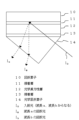
- FIG. 1 is a diagram conceptually showing the configuration of the present invention.
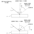
- FIG. 2 is a diagram for explaining the diffraction element.
- FIG. 3 is a diagram for explaining a diffraction element.
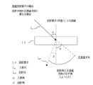
- FIG. 4 is a diagram for explaining a diffraction element.
- FIG. 5 is a diagram for explaining a diffraction element.
- FIG. 6 is a diagram for explaining a method for measuring diffracted light in the embodiment.
- FIG. 7 is a conceptual diagram for explaining a liquid crystal diffraction element.
- a numerical range expressed using “ ⁇ ” means a range that includes the numerical values written before and after " ⁇ " as the lower and upper limits.
- FIG. 1 conceptually shows an example of an optical element of the present invention using an example of a wavelength separation element of the present invention.
- 1 has a diffractive element 10, an adhesive layer 11, an optically anisotropic layer 12, an adhesive layer 13, and a photorefractive element 14.
- the diffractive element 10, the adhesive layer 11, and the optically anisotropic layer 12 constitute the wavelength separation element of the present invention.
- the adhesive layer 11 provided between the diffraction element 10 and the optically anisotropic layer 12 may be an alignment layer.
- the adhesive layer 13 provided between the optically anisotropic layer 12 and the photorefractive element 14 may also be an alignment layer.
- ) by the diffraction element satisfy ⁇
- the case where the direction of the diffracted light is different from the direction toward the specular reflection direction or specular transmission direction from the normal to the plane of the diffraction element is positive (+), and the case where the direction is the same is negative (-).
- the film thickness distribution of the entire wavelength splitting element is within ⁇ 3.0% of the average film thickness, and the surface roughness Ra is 30 nm or less.
- the wavelength separation element of the present invention has such a configuration, and thus realizes a wavelength separation element that has a large diffraction angle and suppresses the spread of diffracted light. This point will be discussed in more detail later.
- a diffraction element 10 diffracts incident light I0, which is a mixture of light of wavelength a and light of wavelength b, and separates the light into diffracted light Ia (wavelength a) and diffracted light Ib (wavelength b).
- the optically anisotropic layer 12 is provided to change the polarization state of the incident light I 0 into a state suitable for the diffraction of light in the diffraction element 10 .
- the diffraction element 10 and the optically anisotropic layer 12 are bonded together by an adhesive layer 11 .
- the optical refraction element 14 is provided to control the angle of incidence of the incident light I0 on the diffraction element 10 and to control the directions of the diffracted light Ia and Ib diffracted by the diffraction element 10.
- a photorefractive element 14 is attached to an optically anisotropic layer 12 by an adhesive layer 13 .
- incident light I0 which is a mixture of light of wavelength a and light of wavelength b, is incident, for example, from the normal direction on one surface of a photorefractive element 14 (e.g., a prism).
- the incident light I0 that has entered the photorefractive element 14 passes through the photorefractive element 14 and the adhesive layer 13, and enters the optically anisotropic layer 12.
- the incident light I 0 incident on the optically anisotropic layer 12 has its polarization state changed, for example by being converted into circularly polarized light, and passes through the optically anisotropic layer 12 , passes through the adhesive layer 11 , and enters the diffraction element 10 .
- the diffraction element 10 is a reflective diffraction element.
- Incident light I0 incident on the diffraction element 10 is reflected and diffracted by the diffraction element 10, and is separated into diffracted light Ia and diffracted light Ib having different diffraction angles according to the wavelengths a and b of the light.
- the diffracted light Ia and the diffracted light Ib separated according to wavelength are transmitted through the adhesive layer 11 and enter the optically anisotropic layer 12.
- the diffracted light Ia and the diffracted light Ib that entered the optically anisotropic layer 12 have their polarization state changed, for example by being converted into linearly polarized light, and then transmit through the optically anisotropic layer 12 and the adhesive layer 13 to enter the photorefractive element 14.
- the diffracted light Ia and diffracted light Ib incident on the optical refraction element 14 have their directions controlled by refraction by the optical refraction element 14, and are transmitted through the optical refraction element 14, and are emitted from the optical element as light of wavelength a (diffracted light Ia ) and light of wavelength b (diffracted light Ib ), each traveling in a different direction.
- the light of wavelength a and the light of wavelength b output from the optical element are incident on an optical fiber constituting an optical transmission network, for example.
- the light of wavelength a and the light of wavelength b are both wavelength-separated by the wavelength separation element of the present invention, and the spread of the light is suppressed. Therefore, the light of wavelength a and the light of wavelength b are all properly incident on the optical fiber without any loss, and are transmitted through the optical transmission network.
- the diffraction element 10 is not limited to a liquid crystal diffraction element, a surface relief type element having a fine uneven pattern, and a volume hologram having a refractive index distribution inside the element.
- Various known diffraction elements can be used.
- a liquid crystal diffraction element is a suitable example.
- a liquid crystal diffraction element formed by using a composition containing a liquid crystal compound and having a predetermined liquid crystal orientation pattern in which the direction of the optical axis derived from the liquid crystal compound continuously rotates toward one direction in the plane is preferably used.
- the liquid crystal diffraction element it is preferable for the liquid crystal diffraction element to have a so-called twist structure in which the orientation of the liquid crystal compound changes continuously from one interface side to the other interface side in the thickness direction, and a cholesteric structure with a short period of the twist structure, from the viewpoints of high efficiency of diffracted light and polarization maintenance, etc.
- the diffraction element may be a reflective diffraction element or a transmissive diffraction element.
- Fig. 7 shows the surface of the liquid crystal layer constituting the liquid crystal diffraction element on the alignment film side.
- this liquid crystal alignment pattern is one in which the direction of the optical axis 40A derived from the liquid crystal compound 40 changes while continuously rotating in one direction within the plane of the liquid crystal layer.
- the optical axis 40A originating from the liquid crystal compound 40 is the slow axis of the liquid crystal compound 40.
- a rod-shaped liquid crystal compound is exemplified as the liquid crystal compound 40
- the optical axis 40A is aligned along the long axis direction of the liquid crystal compound.
- liquid crystal compounds 40 are two-dimensionally aligned in the X and Y directions perpendicular to each other within the plane.
- the orientation of the optical axis 40A changes while continuously rotating along the X direction. That is, the angle between the optical axis 40A of the liquid crystal compound 40 aligned in the X direction and the X direction changes sequentially from ⁇ to ⁇ +180° or ⁇ 180° along the X direction.
- the optical axis 40A has the same orientation.
- the length over which the orientation of the optical axis 40A rotates 180° i.e., the distance ⁇ over which the angle between the optical axis 40A and the X direction changes from ⁇ to ⁇ +180° or ⁇ -180° along the X direction, is one period in the diffraction structure of the liquid crystal diffraction element.
- the distance ⁇ over which the orientation of the optical axis 40A changes continuously from 0° to 180° is one period in the diffraction structure of the liquid crystal diffraction element.
- one period in the diffractive structure of the liquid crystal diffractive element is basically constant.
- the distance ⁇ of one period corresponds to an in-plane pitch a, which will be described later, in the liquid crystal diffraction element.
- the reflective diffraction element is not limited, and various known reflective diffraction elements can be used.
- the in-plane pitch a [nm] i.e., the distance of one period in the diffraction structure of the diffraction element, is determined from the following formula for the first-order diffracted light.
- the shorter the in-plane pitch a i.e., the shorter the period in the diffraction structure, the larger the diffraction angle of light by the diffraction element.
- the optical alignment film can be appropriately exposed to interference based on this.
- n ⁇ a ⁇ (sin ⁇ +sin ⁇ ) ⁇
- the in-plane pitch a is the distance between the liquid crystal compound that changes continuously from 0° to 180° in the plane.
- n is the environmental refractive index on the incident light side in contact with the diffraction element
- ⁇ is the wavelength of the incident light [nm]
- ⁇ is the angle between the light incident on the diffraction element and the normal to the diffraction element surface
- ⁇ is the angle between the reflected diffracted light at the diffraction element and the normal to the diffraction element surface.
- the reflective liquid crystal diffraction element is a cholesteric liquid crystal layer having the above-mentioned liquid crystal orientation pattern. That is, in the case of the reflective liquid crystal diffraction element, it is necessary to have a cholesteric orientation in which the liquid crystal compound is helically twisted and oriented in the thickness direction. In other words, the reflective liquid crystal diffraction element needs to have a structure in which the cholesteric liquid crystal phase is fixed.
- the thickness d [nm] of the liquid crystal layer may be appropriately adjusted according to the required efficiency. For example, in order to improve the light utilization efficiency, the thickness of the liquid crystal layer may be adjusted to be 7 times or more the helical pitch of the cholesteric alignment.
- the cholesteric liquid crystal layer has this helical pitch repeated multiple times, and it is preferable that the helical pitch is repeated 7 times or more.
- a cholesteric liquid crystal layer selectively reflects light in a specific wavelength range depending on the length of the helical pitch of the cholesteric orientation. Specifically, the longer the helical pitch of the cholesteric liquid crystal layer, the more selectively the cholesteric liquid crystal layer reflects light with a longer wavelength. Therefore, the helical pitch of the cholesteric liquid crystal layer can be appropriately determined depending on the wavelength used (the wavelength of the incident light).
- the helical pitch of the cholesteric orientation is the thickness over which the orientation of the liquid crystal compound changes from 0° to 360° in the thickness direction in the helical twisted orientation of the liquid crystal compound in the thickness direction of the cholesteric liquid crystal layer.
- a reflective liquid crystal diffraction element various known reflective liquid crystal diffraction elements such as the liquid crystal diffraction elements described in JP-A-2023-160888 and WO-A-2021-256422 can be used.
- the diffraction element may be a transmission type diffraction element.
- the transmission type diffraction element There is no limitation on the transmission type diffraction element, and various known transmission type diffraction elements can be used.
- the in-plane pitch a [nm] i.e., one period in the diffraction structure of the diffraction element, is determined from the following formula for the first-order diffracted light. Even in a transmission type diffraction element, the shorter the in-plane pitch a, i.e., one period in the diffraction structure, the larger the diffraction angle of light by the diffraction element.
- the optical alignment film can be appropriately exposed to interference based on this.
- n ⁇ a ⁇ (sin ⁇ sin ⁇ ) ⁇
- the in-plane pitch a is the distance between the liquid crystal compound that changes continuously from 0° to 180° in the plane.
- n is the environmental refractive index on the incident light side in contact with the diffraction element
- ⁇ is the wavelength of the incident light [nm]
- ⁇ is the angle between the light incident on the diffraction element and the normal to the diffraction element surface
- ⁇ is the angle between the transmitted diffracted light and the normal to the diffraction element surface.
- the transmissive liquid crystal diffraction element has a liquid crystal layer having the above-mentioned liquid crystal orientation pattern.
- the liquid crystal compound forming the liquid crystal layer and the thickness of the liquid crystal layer can be appropriately selected so that ⁇ n ⁇ d, which is expressed as the product of the refractive index anisotropy ⁇ n ⁇ at a wavelength ⁇ [nm] of the optically anisotropic layer described below and the thickness d [nm] of the liquid crystal layer, becomes ⁇ /2.
- various known transmission type liquid crystal diffraction elements such as the liquid crystal diffraction elements described in International Publication No. 2021/256413 and JP-A-2023-160888 can be used.
- a diffraction element with large diffraction angle refers to a diffraction element in which the angle between the specular reflection direction or specular transmission direction of incident light and the light diffracted by the diffraction element is large, as conceptually shown in Figures 2 to 5.
- the absolute value of the angle ⁇ between the normal to the diffraction element plane and the specular reflection direction or specular transmission direction of incident light, and the absolute value of the diffraction angle ⁇ of the diffraction element satisfy the following formula (1).
- the specular reflection direction is the direction of light reflected at the same angle as the incident light and the normal to the plane of the diffraction element, but in a direction different from the incident light
- the specular transmission direction is the direction of light transmitted through a material in a direction parallel to the incident light.
- is positive (+) when the direction of the diffracted light differs from the direction toward the specular reflection direction or specular transmission direction from the normal to the diffraction element plane, and is negative (-) when the direction is the same.
- formula (1) indicates that the further the direction of the diffracted light is from the direction of specular reflection or the direction of specular transmission, the larger the diffraction angle becomes.
- the film thickness distribution and surface roughness Ra have a significant effect on the spreading and separation of the diffracted light.
- FIG. 2 shows a case where the direction of diffracted light I dif (dashed line) in a reflective diffraction element 10 differs from the regular reflection direction (dashed line) of incident light I in (solid line) with respect to the normal to the plane (surface) of the diffraction element.
- , is 20° or more.
- FIG. 3 shows a case where the direction of diffracted light I dif (dashed line) in a reflective diffraction element 10 is the same as the regular reflection direction (dashed line) of incident light I in (solid line) with respect to the normal to the plane (surface) of the diffraction element.
- of the diffraction angle ⁇ of the diffracted light I dif is 20° or more.
- FIG. 4 shows a case where the direction of diffracted light I dif (dashed line) in a transmission type diffraction element 10 differs from the regular transmission direction (dashed line) of incident light I in (solid line) with respect to the normal to the plane (surface) of the diffraction element.
- , is 20° or more.
- Figure 5 conceptually shows a case in which the direction of diffracted light I dif (dashed line) in a transmission-type diffraction element 10 is the same as the regular transmission direction (dashed line) of incident light I in (solid line) with respect to the normal to the plane (surface) of the diffraction element.
- of the diffraction angle ⁇ of the diffracted light I dif is 20° or more.
- in-plane alignment pattern there is no particular limitation in forming an in-plane orientation pattern necessary for diffraction, and a known method can be used.
- interference exposure using circularly polarized light may be used, as in the exposure apparatus described in FIG. 3 of WO 2021/256413.
- a film containing a photo-alignment material is formed on the surface of a support selected appropriately.
- the film to be the photo-alignment film is subjected to interference exposure with circularly polarized light having an opposite rotation direction using an exposure apparatus described in FIG.
- the optical element of the exposure device may be installed so that the absolute value of the angle of incidence of each interference exposure is the same angle with respect to the normal direction of the photo-alignment film surface.
- the angle at which two circularly polarized light beams with opposite rotation directions that expose the photo-alignment film to interference exposure cross is adjusted.
- the length of the in-plane pitch, or in the case of a liquid crystal diffraction element, the in-plane pitch (the distance ⁇ of one period) in the liquid crystal orientation pattern can be adjusted.
- the smaller the in-plane pitch the larger the diffraction angle of diffracted light.
- the longer the wavelength of light the larger the diffraction angle of the diffracted light.
- the transmission type liquid crystal diffraction element preferably has a twisted structure in which the liquid crystal compound is helically oriented in the thickness direction, and the twist angle of the liquid crystal compound is preferably 360° or less.
- the reflective liquid crystal diffraction element has a cholesteric liquid crystal layer in which the liquid crystal compound is cholesterically aligned, repeating a helical pitch in which the liquid crystal compound is helically aligned by 360° in the thickness direction multiple times.
- the amount of chiral agent added to the liquid crystal composition for forming the liquid crystal layer described in WO 2021/256413 may be appropriately adjusted.
- the diffractive element may be a stack of a plurality of liquid crystal diffractive elements.
- the liquid crystal diffraction element is a reflective diffraction element using a cholesteric liquid crystal layer having the above-mentioned liquid crystal orientation pattern
- the diffraction element may be a laminate in which multiple liquid crystal diffraction elements, each having a cholesteric liquid crystal layer that selectively reflects different wavelength ranges, are stacked together.
- a diffraction element of a laminate in which multiple liquid crystal diffraction elements are stacked a laminate of a reflective liquid crystal diffraction element with a right-handed cholesteric liquid crystal layer and a reflective liquid crystal diffraction element with a left-handed cholesteric liquid crystal layer, a laminate of reflective diffraction elements with different in-plane pitches, and a laminate of elements combining both of these can also be used.
- an optically anisotropic layer 12 is bonded to such a diffraction element 10 via an adhesive layer 11 (alignment film layer).
- the optically anisotropic layer 12 is not particularly limited, and various types can be used.
- an optically anisotropic layer 12 that changes the polarization state of light transmitted through the optically anisotropic layer 12 to a desired polarization state that is, an optically anisotropic layer 12 that changes the polarization state of light incident on the diffraction element 10 to a desired polarization state, is preferably exemplified.
- optically anisotropic layer 12 By using such an optically anisotropic layer 12, it is possible to make it difficult for the polarization state to change due to reflection, refraction, etc., and therefore it is preferable.
- the material for forming the optically anisotropic layer 12 there is no limitation on the material for forming the optically anisotropic layer 12, and known materials such as polymers, liquid crystal compounds, and inorganic substances can be used.
- the diffraction element is a liquid crystal diffraction element, from the viewpoint of reducing the refractive index difference, an optically anisotropic layer using the same type of liquid crystal compound as the liquid crystal diffraction element is more preferable.
- the optically anisotropic layer 12 is preferably a retardation layer, particularly a ⁇ /4 wave plate.
- the incident light can be efficiently diffracted by making circularly polarized light incident thereon.
- a reflective liquid crystal diffraction element cholesteric liquid crystal layer
- the diffraction element 10 is a liquid crystal diffraction element
- a retardation layer in particular a ⁇ /4 wavelength plate
- the light incident on the diffraction element 10 is made circularly polarized, thereby enabling the diffraction element 10 to efficiently diffract the incident light and separate the wavelengths.
- the ⁇ /4 wave plate and a known ⁇ /4 wave plate can be used.
- Examples include a stretched polycarbonate film, a stretched norbornene-based polymer film, a transparent film containing and oriented with inorganic particles having birefringence such as strontium carbonate, a thin film obtained by obliquely depositing an inorganic dielectric on a support, a film in which a polymerizable liquid crystal compound is uniaxially oriented and oriented, and a film in which a liquid crystal compound is uniaxially oriented and oriented.
- a film in which a liquid crystal compound is uniaxially oriented and oriented and oriented is preferably used.
- the wavelength separation element of the present invention is constructed by bonding a diffraction element 10 and an optically anisotropic layer 12 with an adhesive layer 11 .
- a photorefractive element 14 which will be described later, is attached to the optically anisotropic layer 12 by an adhesive layer 13 .
- the adhesive layer 11 is used as a representative example, but the same applies to the adhesive layer 13.
- the adhesive layer 11 adheresive layer 13
- various known adhesives can be used. Examples include a UV adhesive and an adhesive layer using SiOx.
- a pressure sensitive adhesive can also be used for the adhesive layer 11.
- any commercially available adhesive can be used, for example, an epoxy resin adhesive and an acrylic resin adhesive.
- the adhesive layer 11 may also be made of a pressure sensitive adhesive.
- the adhesive and the bonding agent can be selected to have an appropriate viscoelasticity or thickness so as to bury the surface irregularities of the layer to be bonded, from the viewpoint of reducing the surface roughness Ra of the wavelength separation element. From the viewpoint of burying the surface irregularities, the adhesive and the bonding agent preferably have a viscosity of 50 cP or more. In addition, the thickness is preferably thicker than the height of the surface irregularities.
- the adhesive layer 11 (adhesive and pressure-sensitive adhesive) used to bond each layer preferably has a small refractive index difference with adjacent layers, from the viewpoint of reducing unnecessary reflection and suppressing a decrease in the degree of polarization of transmitted light and reflected light.
- the difference in refractive index between the adhesive layer 11 and the adjacent layers is preferably 0.05 or less, more preferably 0.01 or less.
- the refractive index of the pressure sensitive adhesive and the adhesive can be adjusted, for example, by adding and mixing fine particles. Examples of the fine particles to be added include fine particles of titanium oxide and fine particles of zirconia.
- lamination using the adhesive layer 11 made of SiOx can be carried out in the following steps (1) to (3).
- the layers to be laminated are attached to a temporary support made of a glass substrate.
- a SiOx layer having a thickness of 100 nm or less is formed by deposition or the like.
- the deposition can be performed using, for example, a deposition device (model number ULEYES) manufactured by ULVAC, Inc., using SiOx powder as a deposition source.
- a SiOx layer may be formed on the surface of the photorefractive element made of glass.
- the wavelength splitting element of the present invention can be produced, for example, by the following method.
- a liquid crystal diffraction element is used as the diffraction element, but a wavelength separation element using another diffraction element can also be fabricated in accordance with the following method.
- the alignment film and the liquid crystal diffraction element may be formed by a known method according to the forming material, such as the method described above.
- an alignment film is formed on the surface of an appropriately selected support, and an optically anisotropic layer 12 made of, for example, a liquid crystal compound is formed on the alignment film, thereby producing a laminate having the support, the alignment film, and the optically anisotropic layer 12.
- the alignment film and the optically anisotropic layer 12 may be formed by a known method according to the forming materials, such as the above-mentioned method.
- an adhesive that will become the adhesive layer 11 is applied to the formed diffractive element 10 and/or the optically anisotropic layer 12, and the two laminates are laminated with the diffractive element 10 facing the optically anisotropic layer 12.
- the adhesive is cured by a method appropriate for the adhesive, such as ultraviolet irradiation or heating, and the diffractive element 10 and the optically anisotropic layer 12 are bonded together by the adhesive layer 11.
- the alignment film and the support are peeled off from the diffraction element 10, and the alignment film and the support are peeled off from the optically anisotropic layer 12.
- the wavelength separation element of the present invention having the diffraction element 10, the adhesive layer 11, and the optically anisotropic layer 12 is produced.
- the diffraction element 10 liquid crystal diffraction element
- the optically anisotropic layer 12 are formed using a support, for example.
- the support having high rigidity is not particularly limited, but examples thereof include a glass plate and a film with a hard coat.
- the elastic modulus (Young's modulus) of the support is not limited, but is preferably 5 GPa or more, more preferably 25 GPa or more, and even more preferably 50 GPa or more.
- an alignment film layer may be used instead of the adhesive layer 11 .
- a known alignment film such as the above-mentioned photoalignment film can be used depending on the material of the liquid crystal layer to be formed on the alignment film.
- the diffractive element 10 and the optically anisotropic layer 12 are adhered to each other via the alignment film. That is, when forming a layer, the next layer is formed on the already formed layer via the alignment film, so that the adhesive layer can be eliminated.
- an alignment film may be formed on the surface of the optically anisotropic layer, and a liquid crystal diffraction element may be formed as the diffraction element 10 on top of this alignment film.
- an alignment film may be formed on the surface of the diffraction element 10, and an optically anisotropic layer 12 made of a liquid crystal compound may be formed on this alignment film.
- an alignment film may be formed on the surface of the photorefractive element 14, and the optically anisotropic layer 12 made of a liquid crystal compound may be formed on this alignment film.
- the optical element of the present invention comprises such a wavelength separation element of the present invention and a light refraction element.
- 1 includes a wavelength separation element of the present invention having a diffraction element 10, an adhesive layer 11, and an optically anisotropic layer 12, and a photorefractive element 14.
- the optically anisotropic layer 12 and the photorefractive element 14 are bonded together by an adhesive layer 13.
- the optical refractive element 14 is used to control the angle of incidence of light incident on the diffraction element 10 and to control the direction of the diffracted light.
- the light refraction element 14 includes a lens and a prism.
- the wavelength splitting element of the present invention has a film thickness distribution throughout the entire wavelength splitting element within ⁇ 3.0% of the average film thickness, and a surface roughness (Ra) of 30 nm or less.
- the entire wavelength separation element refers to a laminate of the diffractive element, the optically anisotropic layer, and the adhesive layer (or the alignment film layer) therebetween. That is, in the present invention, the entire wavelength separation element refers to the surface of the diffractive element (the side opposite to the adhesive layer) to the surface of the optically anisotropic layer (the side opposite to the adhesive layer).
- the surface roughness Ra refers to the surface roughness Ra of the diffraction element 10 .
- a diffraction element basically has a larger diffraction angle for light with a longer wavelength, and therefore when light containing multiple wavelengths is incident on it, it acts as a wavelength separation element that separates the light according to its wavelength.
- a diffraction element has a large diffraction angle, particularly when the wavelength separation element is a laminate including a diffraction element, the diffracted light may spread, and in severe cases, light of the same wavelength may be separated.
- the inventors of the present invention have conducted extensive research into the cause of this problem.
- the cause of the spread of the diffracted light lies in the film thickness distribution of the entire wavelength splitting element and the surface roughness Ra of the wavelength splitting element.
- the film thickness distribution of the entire wavelength splitting element and the surface roughness Ra of the wavelength splitting element are large, the spread and even separation of the diffracted light occurs.
- a large undulation such as a film thickness distribution can function similarly to a lens with a large radius of curvature (gentle refraction). Therefore, if the film thickness distribution of the wavelength splitting element is large, this can cause the diffracted light to spread.
- the surface roughness Ra corresponding to minute surface irregularities can itself function similarly to a diffraction element. Therefore, if the surface roughness Ra is large, it can cause the diffracted light of a single wavelength to be separated.
- "separation of diffracted light” refers to the separation of diffracted light of a single wavelength.
- the present invention has been made possible by obtaining such knowledge, and the thickness distribution of the entire wavelength separation element is set to within ⁇ 3.0% of the average thickness, and the surface roughness Ra is set to 30 nm or less.
- the wavelength separation element of the present invention realizes a wavelength separation element that suppresses the spread of diffracted light despite having a large diffraction angle. If the film thickness distribution of the entire wavelength separation element exceeds ⁇ 3.0% of the average film thickness, the spread of the diffracted light cannot be sufficiently suppressed, resulting in inconveniences such as the diffracted light not being properly incident on the desired position of the light receiving element such as LCOS or optical fiber, or only a portion of the diffracted light being incident thereon.
- the surface roughness Ra of the wavelength separation element exceeds 30 nm, the spread of the diffracted light cannot be sufficiently suppressed, as described above, resulting in inconveniences such as the diffracted light not being properly incident on the desired position of the light receiving element such as LCOS and optical fiber, or only a portion of the diffracted light being incident thereon.
- the film thickness distribution of the entire wavelength separation element is preferably within ⁇ 2.5% of the average film thickness, and more preferably within ⁇ 2.0% of the average film thickness.
- the surface roughness Ra is preferably 25 nm or less, and more preferably 20 nm or less.
- the film thickness distribution of the entire wavelength separation element is preferably at least ⁇ 0.5% of the average film thickness.
- the surface roughness Ra of the wavelength separation element of the present invention is preferably at least 1 nm.
- a wavelength separation element having a diffraction element and an optically anisotropic layer, and an adhesive layer (alignment film layer) therebetween if the film thickness distribution and surface roughness Ra of each component constituting the wavelength separation element are large, the diffracted light may spread and separate as described above.
- the diffraction element, adhesive layer (alignment film layer) and optically anisotropic layer also have small film thickness distribution and surface roughness Ra.
- each of these members has a film thickness distribution within ⁇ 2.0% of the average film thickness and a surface roughness Ra of 20 nm or less.
- the wavelength separation element of the present invention is preferable in that by satisfying such conditions, the spread of diffracted light can be more suitably suppressed, the separation of diffracted light can be more suitably suppressed, and the diffracted light can be correctly incident on a desired position of a light receiving element such as an LCOS or an optical fiber.
- the thickness distribution of each member constituting the wavelength splitting element is more preferably within ⁇ 1.5% of the average thickness, and even more preferably within ⁇ 1.0% of the average thickness.
- the surface roughness Ra of each member constituting the wavelength splitting element is more preferably 15 nm or less, and even more preferably 10 nm or less.
- a wavelength separation element having a diffraction element and an optically anisotropic layer, and an adhesive layer (alignment film layer) therebetween there is no limitation on the method for fabricating a wavelength separation element whose film thickness distribution and surface roughness Ra satisfy the above-mentioned conditions, and various methods can be used.
- a method is exemplified in which a support having high surface smoothness and high rigidity (elastic modulus), such as a glass plate or a film with a hard coat layer, is used as a support for forming a diffraction element, particularly a liquid crystal diffraction element, and an optically anisotropic layer, particularly an optically anisotropic layer made of a liquid crystal compound.
- an optically anisotropic layer made of a liquid crystal diffraction element and a liquid crystal compound when forming an optically anisotropic layer made of a liquid crystal diffraction element and a liquid crystal compound, if a general resin film such as a PET (polyethylene terephthalate) film is used as a support for forming at least one of them, the overall film thickness distribution and/or surface roughness Ra tend to become large.
- a glass plate or the like as a support for forming an optically anisotropic layer made of a liquid crystal diffraction element and a liquid crystal compound, a wavelength separation element having the above-mentioned film thickness distribution and surface roughness Ra can be stably produced.
- the order of steps for laminating the respective members there is no particular limitation on the order of steps for laminating the respective members, and the order can be selected arbitrarily.
- the order of lamination can also be selected from the standpoint of quality evaluation, manufacturing yield, cost reduction, and the like.
- a clean room, a static electricity removing fan, an air spray, and the like can be used as appropriate when producing each member and bonding the members.
- the film thickness of the wavelength splitting element can be measured, for example, by observing the cross section of the entire wavelength splitting element and each layer of its constituent members using an optical microscope, a SEM (Scanning Electron Microscope), or the like. Specifically, the cross section of the entire wavelength separation element is imaged using an SEM or the like to obtain image data for multiple cross sections (e.g., five cross sections) at different locations, and the positions of the upper and lower end faces are extracted at multiple positions in each image data from the multiple image data measured at different locations on the cross section, thereby making it possible to calculate the film thickness distribution, average film thickness, etc.
- the surface roughness Ra (arithmetic mean roughness) can be measured using a commercially available measuring instrument such as a non-contact surface/layer cross-sectional shape measuring system VertScan (manufactured by Ryoka Systems Co., Ltd.).
- composition 1 As a liquid crystal composition for forming a liquid crystal diffraction element, the following composition 1 was prepared.
- Rod-shaped liquid crystal compound L-1 100.00 parts by mass Photopolymerization initiator (KAYACURE DETX-S, manufactured by Nippon Kayaku Co., Ltd.) 1.00 parts by mass Chiral agent Ch-1 1.70 parts by mass Methyl ethyl ketone 142.06 parts by mass
- Rod-shaped liquid crystal compound L-1 (containing the following structures in the mass ratios shown on the right)
- composition containing a photo-alignment material SD-1, DIC
- a glass support EagleXG, Cornings
- This coating film was subjected to interference exposure using the exposure device shown in Figure 3 of WO 2021/256413 to form a photo-alignment film.
- the above-mentioned composition 1 was applied to the photo-alignment film, dried, and UV-cured under a nitrogen atmosphere to form a reflective liquid crystal diffraction element.
- Rod-shaped liquid crystal compound L-1 100.00 parts by mass Photopolymerization initiator (KAYACURE DETX-S, manufactured by Nippon Kayaku Co., Ltd.) 1.00 part by mass, Surfactant-1, 0.20 part by mass, Methyl ethyl ketone, 142.06 parts by mass
- composition containing a photoalignment material was applied to a glass support (manufactured by Cornings, Eagle XG, elastic modulus 77 GPa) and dried. This coating film was exposed to polarized UV light to form a photoalignment film.
- the above-mentioned composition 2 was applied to the formed photo-alignment film and dried, and then the composition 2 was cured with UV light in a nitrogen atmosphere to form an optically anisotropic layer.
- Example 1 An optically anisotropic layer was formed in the same manner as in Example 1, except that a PET film (manufactured by Fuji Film Co., Ltd., thickness 50 ⁇ m) was used instead of a glass plate as a support for forming the optically anisotropic layer.
- a PET film manufactured by Fuji Film Co., Ltd., thickness 50 ⁇ m
- Comparative Example 2 An optically anisotropic layer was formed in the same manner as in Example 1, except that the optically anisotropic layer (Composition 2) was dried while being exposed to strong air.
- Example 3 An optically anisotropic layer was formed in the same manner as in Example 1, except that a PET film (manufactured by Fujifilm, film thickness 50 ⁇ m) was used instead of a glass plate as a support for forming the optically anisotropic layer, and the optically anisotropic layer (Composition 2) was dried while being exposed to strong wind.
- a PET film manufactured by Fujifilm, film thickness 50 ⁇ m
- the optically anisotropic layer Composition 2
- a wavelength separation element of Comparative Example 1 was produced in the same manner as in Example 1, except that an optically anisotropic layer formed using a support made of a PET film was used.
- a wavelength separation element of Comparative Example 2 was prepared in the same manner as in Example 1, except that an optically anisotropic layer was used, which was formed by using a glass support and drying the support while applying strong wind.
- a wavelength separation element of Comparative Example 3 was prepared in the same manner as in Example 1, except that a support made of a PET film was used and an optically anisotropic layer formed by drying under exposure to strong air was used.
- the surface roughness Ra and film thickness distribution of the fabricated wavelength splitting element were measured.
- the surface roughness Ra was measured using a VertScan (manufactured by Ryoka Systems Co., Ltd.)
- the surface roughness Ra was measured on the surface of the diffraction element.
- the film thickness distribution was calculated from five SEM images of the cross section of a cut portion of the fabricated wavelength separation element. The positions of the upper and lower interfaces of the SEM images were profiled by image processing, and the film thickness at each position was calculated from the position information (100 data/sheet) and magnification, and the average of these was taken as the average film thickness (average film thickness).
- the film thickness distribution was calculated from the following formula. + side film thickness distribution: 100 x (maximum film thickness - average film thickness) / (average film thickness) -side thickness distribution: 100 x (minimum thickness - average thickness) / (average thickness)
- the incident angle of the incident light I in was 45°. That is, the absolute value of the angle ⁇ (
- the direction of the diffracted light I dif is different from the direction toward the regular reflection direction with respect to the normal to the plane of the diffraction element. Therefore, in this example,
- 95.3° It is.
Landscapes
- Physics & Mathematics (AREA)
- General Physics & Mathematics (AREA)
- Optics & Photonics (AREA)
- Diffracting Gratings Or Hologram Optical Elements (AREA)
Abstract
大きな回折角を有する回折素子を用いた場合でも、回折光の広がりを抑えた波長分離素子、および、これを用いる光学素子の提供を目的とする。回折素子と、光学異方性層と、両者の間にある接着層または配向膜層とを有し、回折素子平面の法線と入射光の正反射または正透過方向とのなす角αの絶対値および回折素子の回折角βの絶対値が、式『||α|±|β||≧20°』を満たし、波長分離素子全体の膜厚分布が平均膜厚の±3.0%以内、かつ、表面粗さ(Ra)が30nm以下である波長分離素子により、課題を解決する。なお、上記式において、回折光の方向が、回折素子平面の法線から正反射方向もしくは正透過方向に向かう方向と異なる場合が正(+)、同じ場合が負(-)である。
Description
本発明は、光通信技術の分野に関し、特に波長分離素子、および、この波長分離素子を用いる光学素子に関する。
光伝送ネットワークにおいて、ネットワークの容量拡大に対応するため、波長多重通信で使用される光波長選択スイッチ(Wavelength Selective Switch,WSS)の高性能化、および、装置の小型化による使用可能台数の増加等が求められる。
その装置内において、入射される光の波長を切り分け、適切な方向に振り分けるために、波長分離素子とLCOS(Liquid crystal on silicon)との組み合わせなどに代表される光方向制御装置が用いられている。
このような光方向制御装置には、各波長の光の損失をできる限り少なく、出射側の光ファイバーに入れることが求められる。
このような光方向制御装置には、各波長の光の損失をできる限り少なく、出射側の光ファイバーに入れることが求められる。
近年、装置の高性能化および小型化に伴い、特に回折角の大きい波長分離素子を用いられることがある。このような波長分離素子において、回折素子そのもの、あるいは、回折素子が貼合された光学部材による回折光に広がりがあると、光ファイバーに入らない光が存在するため、エネルギー損失になってしまう。
本発明者らによる鋭意検討の結果、この回折光の広がりは、回折素子そのもの、および、回折素子が貼合された光学部材の平滑性に起因することがわかった。
本発明者らによる鋭意検討の結果、この回折光の広がりは、回折素子そのもの、および、回折素子が貼合された光学部材の平滑性に起因することがわかった。
本発明の目的は、大きな回折角を有する回折素子を用いた場合でも、回折光の広がりを抑えることができる波長分離素子、および、この波長分離素子を用いる光学素子を提供することにある。
本発明者らは、以下の構成により、上記課題が解決できることを見出した。
[1] 少なくとも、回折素子と、光学異方性層と、それらの間にある接着層、もしくは、配向膜層とを有する波長分離素子であって、
回折素子は、回折素子平面の法線と入射光の正反射方向もしくは正透過方向とがなす角αの絶対値(|α|)、および、回折素子の回折角βの絶対値(|β|)が、式(1)を満たす回折素子であり、
波長分離素子全体の膜厚分布が平均膜厚の±3.0%以内、かつ、表面粗さ(Ra)が30nm以下である
波長分離素子。
||α|±|β||≧20° ・・・式(1)
ここで、回折光の方向が、回折素子平面の法線から正反射方向もしくは正透過方向に向かう方向と異なる場合が正(+)、同じ場合が負(-)である。
[2] 回折素子が液晶回折素子である、[1]に記載の波長分離素子。
[3] 回折素子が複数の液晶回折素子の積層体である、[1]または[2]に記載の波長分離素子。
[4] 光学異方性層が液晶化合物からなる、[1]~[3]のいずれかに記載の波長分離素子。
[5] 光学異方性層が液晶化合物からなり、かつ、λ/4板である、[1]~[4]のいずれかに記載の波長分離素子。
[6] [1]~[5]のいずれかに記載の波長分離素子と、光屈折素子とを有する光学素子
回折素子は、回折素子平面の法線と入射光の正反射方向もしくは正透過方向とがなす角αの絶対値(|α|)、および、回折素子の回折角βの絶対値(|β|)が、式(1)を満たす回折素子であり、
波長分離素子全体の膜厚分布が平均膜厚の±3.0%以内、かつ、表面粗さ(Ra)が30nm以下である
波長分離素子。
||α|±|β||≧20° ・・・式(1)
ここで、回折光の方向が、回折素子平面の法線から正反射方向もしくは正透過方向に向かう方向と異なる場合が正(+)、同じ場合が負(-)である。
[2] 回折素子が液晶回折素子である、[1]に記載の波長分離素子。
[3] 回折素子が複数の液晶回折素子の積層体である、[1]または[2]に記載の波長分離素子。
[4] 光学異方性層が液晶化合物からなる、[1]~[3]のいずれかに記載の波長分離素子。
[5] 光学異方性層が液晶化合物からなり、かつ、λ/4板である、[1]~[4]のいずれかに記載の波長分離素子。
[6] [1]~[5]のいずれかに記載の波長分離素子と、光屈折素子とを有する光学素子
本発明によれば、回折光の広がりを抑えた回折角の大きい波長分離素子、および、この波長分離素子を用いる光学素子を提供できる。
以下、本発明の波長分離素子および光学素子について、添付の図面に示される好適実施形態を基に詳細に説明する。
本明細書において「~」を用いて表される数値範囲は、「~」の前後に記載される数値を下限値および上限値として含む範囲を意味する。
図1に、本発明の波長分離素子の一例を用いる、本発明の光学素子の一例を概念的に示す。
図1に示す光学素子は、回折素子10と、接着層11と、光学異方性層12と、接着層13と、光屈折素子14とを有する。この光学素子においては、回折素子10、接着層11、および、光学異方性層12が、本発明の波長分離素子を構成する。
なお、本発明の波長分離素子において、回折素子10と光学異方性層12との間に設けられる接着層11は、配向膜層であってもよい。同様に、本発明の光学素子において、光学異方性層12と光屈折素子14との間に設けられる接着層13も、配向膜層であってもよい。
図1に示す光学素子は、回折素子10と、接着層11と、光学異方性層12と、接着層13と、光屈折素子14とを有する。この光学素子においては、回折素子10、接着層11、および、光学異方性層12が、本発明の波長分離素子を構成する。
なお、本発明の波長分離素子において、回折素子10と光学異方性層12との間に設けられる接着層11は、配向膜層であってもよい。同様に、本発明の光学素子において、光学異方性層12と光屈折素子14との間に設けられる接着層13も、配向膜層であってもよい。
ここで、本発明の波長分離素子は、回折素子が、回折素子の平面(表面)の法線と、入射光の正反射方向もしくは正透過方向とがなす角αの絶対値(|α|)、および、回折素子による回折角βの絶対値(|β|)が、『||α|±|β||≧20°』を満たす。なお、この式においては、回折光の方向が、回折素子の平面の法線から正反射方向もしくは正透過方向に向かう方向と異なる場合が正(+)、同じ場合が負(-)である。
さらに、本発明の波長分離素子は、波長分離素子全体の膜厚分布が平均膜厚の±3.0%以内であり、かつ、表面粗さRaが30nm以下である。
本発明の波長分離素子は、このような構成を有することにより、回折角が大きく、かつ、回折光の広がりを抑制した波長分離素子を実現している。
この点に関しては、後に詳述する。
さらに、本発明の波長分離素子は、波長分離素子全体の膜厚分布が平均膜厚の±3.0%以内であり、かつ、表面粗さRaが30nm以下である。
本発明の波長分離素子は、このような構成を有することにより、回折角が大きく、かつ、回折光の広がりを抑制した波長分離素子を実現している。
この点に関しては、後に詳述する。
図1に示す波長分離素子において、回折素子10は、波長aの光と波長bの光とが混合した入射光I0を回折して、回折光Ia(波長a)と回折光Ib(波長b)とに分離する。
また、光学異方性層12は、入射光I0の偏光状態を、回折素子10における光の回折に適切な状態に変えるために設けられる。
波長分離素子において、回折素子10と光学異方性層12とは、接着層11によって貼合される。
また、図1に示す光学素子において、光屈折素子14は、入射光I0の回折素子10への入射角の制御、および、回折素子10が回折した回折光Iaおよび回折光Ibの方向を制御するために設けられる。
光学素子において、光屈折素子14は、接着層13によって、光学異方性層12に貼合される。
また、光学異方性層12は、入射光I0の偏光状態を、回折素子10における光の回折に適切な状態に変えるために設けられる。
波長分離素子において、回折素子10と光学異方性層12とは、接着層11によって貼合される。
また、図1に示す光学素子において、光屈折素子14は、入射光I0の回折素子10への入射角の制御、および、回折素子10が回折した回折光Iaおよび回折光Ibの方向を制御するために設けられる。
光学素子において、光屈折素子14は、接着層13によって、光学異方性層12に貼合される。
図1に示す光学素子において、波長aの光と波長bの光とが混合した入射光I0は、例えば、光屈折素子14(例えばプリズム)の一面に法線方向から入射する。光屈折素子14にした入射光I0は、光屈折素子14および接着層13を透過して、光学異方性層12に入射する。
光学異方性層12に入射した入射光I0は、例えば円偏光に変換される等、偏光状態を変更されて光学異方性層12を透過し、接着層11を透過して回折素子10に入射する。
図1に示す光学素子(波長分離素子)においては、一例して、回折素子10は反射型の回折素子である。回折素子10に入射した入射光I0は、回折素子10によって反射されると共に回折されて、光の波長aおよび波長bに応じて、回折角が異なる回折光Iaと回折光Ibとに分離される。
波長に応じて分離された回折光Iaおよび回折光Ibは、接着層11を透過して光学異方性層12に入射する。光学異方性層12に入射した回折光Iaおよび回折光Ibは、例えば直線偏光に変換される等、偏光状態を変更されて光学異方性層12を透過し、接着層13を透過して、光屈折素子14に入射する。
光屈折素子14に入射した回折光Iaおよび回折光Ibは、光屈折素子14による屈折によって進行方向を制御されて光屈折素子14を透過し、それぞれ、進行方向が異なる波長aの光(回折光Ia)および波長bの光(回折光Ib)として、光学素子から出射される。
光学素子から出射された波長aの光および波長bの光は、一例として、光伝送ネットワークを構成する光ファイバーに入射する。ここで、波長aの光および波長bの光は、共に、本発明の波長分離素子によって波長分離されたものであり、光の広がりを抑制されいる。従って、波長aの光および波長bの光は、共に、損失を生じることなく、全てが適正に光ファイバーに入射して、光伝送ネットワークを伝送される。
光学異方性層12に入射した入射光I0は、例えば円偏光に変換される等、偏光状態を変更されて光学異方性層12を透過し、接着層11を透過して回折素子10に入射する。
図1に示す光学素子(波長分離素子)においては、一例して、回折素子10は反射型の回折素子である。回折素子10に入射した入射光I0は、回折素子10によって反射されると共に回折されて、光の波長aおよび波長bに応じて、回折角が異なる回折光Iaと回折光Ibとに分離される。
波長に応じて分離された回折光Iaおよび回折光Ibは、接着層11を透過して光学異方性層12に入射する。光学異方性層12に入射した回折光Iaおよび回折光Ibは、例えば直線偏光に変換される等、偏光状態を変更されて光学異方性層12を透過し、接着層13を透過して、光屈折素子14に入射する。
光屈折素子14に入射した回折光Iaおよび回折光Ibは、光屈折素子14による屈折によって進行方向を制御されて光屈折素子14を透過し、それぞれ、進行方向が異なる波長aの光(回折光Ia)および波長bの光(回折光Ib)として、光学素子から出射される。
光学素子から出射された波長aの光および波長bの光は、一例として、光伝送ネットワークを構成する光ファイバーに入射する。ここで、波長aの光および波長bの光は、共に、本発明の波長分離素子によって波長分離されたものであり、光の広がりを抑制されいる。従って、波長aの光および波長bの光は、共に、損失を生じることなく、全てが適正に光ファイバーに入射して、光伝送ネットワークを伝送される。
(回折素子)
本発明の波長分離素子において、回折素子10は、これに限定されるものではないが、液晶回折素子、微細な凹凸パターンを有する表面レリーフ型素子、および、素子内部に屈折率分布を有する体積ホログラム等に代表される公知の回折素子が、各種、利用可能である。
中でも、液晶回折素子は好適に例示される。特に液晶回折素子としては、液晶化合物を含む組成物を用いて形成された、液晶化合物由来の光学軸の向きが、面内の一方向に向かって連続的に回転する所定の液晶配向パターンを有する液晶回折素子が好適に用いられる。
また、液晶回折素子は、厚さ方向において、液晶化合物の向きが一方の界面側から他方の界面側へ連続的に変化する、いわゆる、ツイスト構造(ねじれ構造)、および、ツイスト構造の周期の短いコレステリック構造を有すると、回折光の高効率化および偏光維持性等の観点で好ましい。
本発明の波長分離素子において、回折素子は、反射型の回折素子でも、透過型の回折素子でもよい。
本発明の波長分離素子において、回折素子10は、これに限定されるものではないが、液晶回折素子、微細な凹凸パターンを有する表面レリーフ型素子、および、素子内部に屈折率分布を有する体積ホログラム等に代表される公知の回折素子が、各種、利用可能である。
中でも、液晶回折素子は好適に例示される。特に液晶回折素子としては、液晶化合物を含む組成物を用いて形成された、液晶化合物由来の光学軸の向きが、面内の一方向に向かって連続的に回転する所定の液晶配向パターンを有する液晶回折素子が好適に用いられる。
また、液晶回折素子は、厚さ方向において、液晶化合物の向きが一方の界面側から他方の界面側へ連続的に変化する、いわゆる、ツイスト構造(ねじれ構造)、および、ツイスト構造の周期の短いコレステリック構造を有すると、回折光の高効率化および偏光維持性等の観点で好ましい。
本発明の波長分離素子において、回折素子は、反射型の回折素子でも、透過型の回折素子でもよい。
図7に、液晶回折素子における、上述の液晶配向パターンを概念的に示す。図7は、液晶回折素子を構成する液晶層の配向膜側の面を示している。
上述のように、この液晶配向パターンは、液晶化合物40に由来する光学軸40Aの向きが、液晶層の面内において、一方向に連続的に回転しながら変化する液晶配向パターンである。
なお、液晶化合物40に由来する光学軸40Aとは、液晶化合物40における遅相軸である。図7では、液晶化合物40として棒状液晶化合物を例示しているので、光学軸40Aは、液晶化合物の長軸方向に沿っている。
図7に示すように、この液晶配向パターンを有する液晶層では、液晶化合物40は、面内において、直交するX方向とY方向とに二次元的に配列されたような状態となっている。
上述のように、この液晶配向パターンは、液晶化合物40に由来する光学軸40Aの向きが、液晶層の面内において、一方向に連続的に回転しながら変化する液晶配向パターンである。
なお、液晶化合物40に由来する光学軸40Aとは、液晶化合物40における遅相軸である。図7では、液晶化合物40として棒状液晶化合物を例示しているので、光学軸40Aは、液晶化合物の長軸方向に沿っている。
図7に示すように、この液晶配向パターンを有する液晶層では、液晶化合物40は、面内において、直交するX方向とY方向とに二次元的に配列されたような状態となっている。
図示例の液晶層では、X方向に向かって、光学軸40Aの向きが連続的に回転しながら変化する。すなわち、X方向に配列されている液晶化合物40の光学軸40Aと、X方向とが成す角度が、X方向に沿って、θからθ+180°あるいはθ-180°まで、順次、変化している。
他方、X方向と直交するY方向では、光学軸40Aの向きが等しい。
X方向において、光学軸40Aの向きが180°回転する長さ、すなわち、光学軸40Aと、X方向とが成す角度が、X方向に沿って、θからθ+180°あるいはθ-180°まで変化する間の距離Λが、液晶回折素子の回折構造における1周期である。言い換えると、X方向のある位置における光学軸40Aの向きを0°とした際に、光学軸40Aの向きが0°から180°まで連続的に変化する間の距離Λが、液晶回折素子の回折構造における1周期である。
なお、本発明においては、液晶回折素子の回折構造における1周期は、基本的に、一定である。
この1周期の距離Λが、液晶回折素子において、後述する面内ピッチaに相当する。
他方、X方向と直交するY方向では、光学軸40Aの向きが等しい。
X方向において、光学軸40Aの向きが180°回転する長さ、すなわち、光学軸40Aと、X方向とが成す角度が、X方向に沿って、θからθ+180°あるいはθ-180°まで変化する間の距離Λが、液晶回折素子の回折構造における1周期である。言い換えると、X方向のある位置における光学軸40Aの向きを0°とした際に、光学軸40Aの向きが0°から180°まで連続的に変化する間の距離Λが、液晶回折素子の回折構造における1周期である。
なお、本発明においては、液晶回折素子の回折構造における1周期は、基本的に、一定である。
この1周期の距離Λが、液晶回折素子において、後述する面内ピッチaに相当する。
(反射型回折素子)
本発明の波長分離素子において、反射型の回折素子には制限はなく、公知の反射型回折素子が、各種、利用可能である。
反射型回折素子の場合、下記の1次回折光の式から、面内ピッチa[nm]すなわち回折素子の回折構造における1周期の距離を決める。反射型回折素子では、面内ピッチaすなわち回折構造における1周期が短いほど、回折素子による光の回折角度が大きくなる。反射型の液晶回折素子の場合、それに基づいて光配向膜を、適宜、干渉露光すればよい。
n×a×(sinβ+sinα)=λ
ここで、液晶回折素子の場合、上述のように、面内ピッチaは、液晶化合物が面内で0°から180°連続的に変化する間の距離である。
また、nは回折素子の接する入射光側の環境屈折率、λは入射光の波長[nm]、αは回折素子に入射する光と回折素子表面の法線とがなす角度、βは回折素子での反射回折光と回折素子表面の法線とがなす角度である。
本発明の波長分離素子において、反射型の回折素子には制限はなく、公知の反射型回折素子が、各種、利用可能である。
反射型回折素子の場合、下記の1次回折光の式から、面内ピッチa[nm]すなわち回折素子の回折構造における1周期の距離を決める。反射型回折素子では、面内ピッチaすなわち回折構造における1周期が短いほど、回折素子による光の回折角度が大きくなる。反射型の液晶回折素子の場合、それに基づいて光配向膜を、適宜、干渉露光すればよい。
n×a×(sinβ+sinα)=λ
ここで、液晶回折素子の場合、上述のように、面内ピッチaは、液晶化合物が面内で0°から180°連続的に変化する間の距離である。
また、nは回折素子の接する入射光側の環境屈折率、λは入射光の波長[nm]、αは回折素子に入射する光と回折素子表面の法線とがなす角度、βは回折素子での反射回折光と回折素子表面の法線とがなす角度である。
反射型の液晶回折素子は、上述した液晶配向パターンを有するコレステリック液晶層である。すなわち、反射型の液晶回折素子の場合、厚さ方向において、液晶化合物が螺旋状に捩れ配向するコレステリック配向を有している必要がある。言い換えれば、反射型の液晶回折素子は、コレステリック液晶相を固定してなる構造を有する必要がある。
また、コレステリック液晶層において、液晶層の膜厚d[nm]は、必要な効率に合わせて、適宜調節すればよい。
例えば、光の利用効率を高めるためには、コレステリック配向の螺旋ピッチの7倍以上になるように液晶層の厚さを調節すればよい。すなわち、コレステリック液晶層は、この螺旋ピッチを、複数回、繰り返して有するものであり、螺旋ピッチを7回以上、繰り返すのが好ましい。
周知のように、コレスtリック液晶層は、コレステリック配向の螺旋ピッチの長さに応じて、特定の波長域の光を選択的に反射する。具体的には、コレステリック液晶層は、螺旋ピッチが長いほど、長波長の光を選択的に反射する。従って、コレステリック液晶層の螺旋ピッチは、使用する波長(入射光の波長)によって、適宜、決めればよい。
なお、コレステリック配向の螺旋ピッチとは、具体的には、コレステリック液晶層の厚さ方向における液晶化合物の螺旋状の捩れ配向において、厚さ方向に、液晶化合物の向きが0°から360°変化する間の厚さである。
このような反射型の液晶回折素子は、例えば、特開2023-160888号公報および国際公開第2021-256422号に記載される液晶回折素子等、公知の反射型の液晶回折素子が、各種、利用可能である。
また、コレステリック液晶層において、液晶層の膜厚d[nm]は、必要な効率に合わせて、適宜調節すればよい。
例えば、光の利用効率を高めるためには、コレステリック配向の螺旋ピッチの7倍以上になるように液晶層の厚さを調節すればよい。すなわち、コレステリック液晶層は、この螺旋ピッチを、複数回、繰り返して有するものであり、螺旋ピッチを7回以上、繰り返すのが好ましい。
周知のように、コレスtリック液晶層は、コレステリック配向の螺旋ピッチの長さに応じて、特定の波長域の光を選択的に反射する。具体的には、コレステリック液晶層は、螺旋ピッチが長いほど、長波長の光を選択的に反射する。従って、コレステリック液晶層の螺旋ピッチは、使用する波長(入射光の波長)によって、適宜、決めればよい。
なお、コレステリック配向の螺旋ピッチとは、具体的には、コレステリック液晶層の厚さ方向における液晶化合物の螺旋状の捩れ配向において、厚さ方向に、液晶化合物の向きが0°から360°変化する間の厚さである。
このような反射型の液晶回折素子は、例えば、特開2023-160888号公報および国際公開第2021-256422号に記載される液晶回折素子等、公知の反射型の液晶回折素子が、各種、利用可能である。
(透過型回折素子)
一方、回折素子は透過型回折素子でもよい。透過型回折素子には、制限はなく、公知の透過型回折素子が、各種、利用可能である。
透過型回折素子の場合、下記の1次回折光の式から、面内ピッチa[nm]すなわち回折素子の回折構造における1周期を決める。透過型回折素子においても、面内ピッチaすなわち回折構造における1周期が短いほど、回折素子による光の回折角度が大きくなる。液晶回折素子の場合、それに基づいて光配向膜を、適宜、干渉露光すればよい。
n×a×(sinβ-sinα)=λ
上述のように、液晶回折素子の場合、面内ピッチaは、液晶化合物が面内で0°から180°連続的に変化する間の距離である。
また、nは回折素子の接する入射光側の環境屈折率、λは入射光の波長[nm]、αは回折素子に入射する光と回折素子表面の法線とのなす角度、βは透過回折光と回折素子表面の法線とのなす角度である。
一方、回折素子は透過型回折素子でもよい。透過型回折素子には、制限はなく、公知の透過型回折素子が、各種、利用可能である。
透過型回折素子の場合、下記の1次回折光の式から、面内ピッチa[nm]すなわち回折素子の回折構造における1周期を決める。透過型回折素子においても、面内ピッチaすなわち回折構造における1周期が短いほど、回折素子による光の回折角度が大きくなる。液晶回折素子の場合、それに基づいて光配向膜を、適宜、干渉露光すればよい。
n×a×(sinβ-sinα)=λ
上述のように、液晶回折素子の場合、面内ピッチaは、液晶化合物が面内で0°から180°連続的に変化する間の距離である。
また、nは回折素子の接する入射光側の環境屈折率、λは入射光の波長[nm]、αは回折素子に入射する光と回折素子表面の法線とのなす角度、βは透過回折光と回折素子表面の法線とのなす角度である。
透過型液晶回折素子は、上述した液晶配向パターンを有する液晶層を有するものである。
また、透過型の液晶回折素子の場合、後述する光学異方性層の波長λ[nm]における屈折率異方性Δnλと、液晶層の膜厚d[nm]の積で表される、Δnλ×dがλ/2となるように、適宜、液晶層を形成する液晶化合物および液晶層の膜厚を選択すればよい。
このような透過型の液晶回折素子は、例えば、国際公開第2021/256413号および特開2023-160888号公報に記載される液晶回折素子等、公知の透過型の液晶回折素子が、各種、利用可能である。
また、透過型の液晶回折素子の場合、後述する光学異方性層の波長λ[nm]における屈折率異方性Δnλと、液晶層の膜厚d[nm]の積で表される、Δnλ×dがλ/2となるように、適宜、液晶層を形成する液晶化合物および液晶層の膜厚を選択すればよい。
このような透過型の液晶回折素子は、例えば、国際公開第2021/256413号および特開2023-160888号公報に記載される液晶回折素子等、公知の透過型の液晶回折素子が、各種、利用可能である。
(回折角が大きい回折素子)
本発明において、回折角の大きい回折素子とは、図2~図5に概念的に示すように、入射光の正反射方向もしくは正透過方向と、回折素子による回折光とがなす角が大きいことをいう。具体的には、回折素子平面の法線と、入射光の正反射方向もしくは正透過方向とがなす角αの絶対値、および、回折素子の回折角βの絶対値が、下記の式(1)を満たすことである。
||α|±|β||≧20°・・・式(1)
ここで、正反射方向とは、入射光と回折素子平面の法線のなす角と同じ角度で、かつ、入射光とは異なる方向に反射する光の方向のことである。また、正透過方向とは、入射光と平行な方向に、物質を透過する光の方向のことである。
さらに、||α|±|β||において、回折光の方向が、回折素子平面の法線から正反射方向もしくは正透過方向に向かう方向と異なる場合が正(+)、同じ場合が負(-)である。
つまり、式(1)は、回折光の方向が、正反射方向もしくは正透過方向から離れるほど、回折角が大きいことを表している。このような回折角が大きい回折素子を用いる場合、膜厚分布および表面粗さRaが、回折光の広がりおよび分離により顕著に影響する。
本発明において、回折角の大きい回折素子とは、図2~図5に概念的に示すように、入射光の正反射方向もしくは正透過方向と、回折素子による回折光とがなす角が大きいことをいう。具体的には、回折素子平面の法線と、入射光の正反射方向もしくは正透過方向とがなす角αの絶対値、および、回折素子の回折角βの絶対値が、下記の式(1)を満たすことである。
||α|±|β||≧20°・・・式(1)
ここで、正反射方向とは、入射光と回折素子平面の法線のなす角と同じ角度で、かつ、入射光とは異なる方向に反射する光の方向のことである。また、正透過方向とは、入射光と平行な方向に、物質を透過する光の方向のことである。
さらに、||α|±|β||において、回折光の方向が、回折素子平面の法線から正反射方向もしくは正透過方向に向かう方向と異なる場合が正(+)、同じ場合が負(-)である。
つまり、式(1)は、回折光の方向が、正反射方向もしくは正透過方向から離れるほど、回折角が大きいことを表している。このような回折角が大きい回折素子を用いる場合、膜厚分布および表面粗さRaが、回折光の広がりおよび分離により顕著に影響する。
図2に、反射型の回折素子10において、回折光Idif(一点鎖線)の方向が、回折素子の平面(表面)の法線に対して、入射光Iin(実線)の正反射方向(二点鎖線)と異なる場合を示す。
この場合には、図2に示すように、回折素子の平面(表面)の法線(破線)と入射光Iinの正反射方向とが成す角αの絶対値|α|と、回折光Idifの回折角βの絶対値|β|との和である||α|+|β||が20°以上である。
この場合には、図2に示すように、回折素子の平面(表面)の法線(破線)と入射光Iinの正反射方向とが成す角αの絶対値|α|と、回折光Idifの回折角βの絶対値|β|との和である||α|+|β||が20°以上である。
図3に、反射型の回折素子10において、回折光Idif(一点鎖線)の方向が、回折素子の平面(表面)の法線に対して、入射光Iin(実線)の正反射方向(二点鎖線)と同じ場合を示す。
この場合には、図3に示すように、回折素子の平面(表面)の法線(破線)と入射光Iinの正反射方向とが成す角αの絶対値|α|と、回折光Idifの回折角βの絶対値|β|との差である||α|-|β||が20°以上である。
この場合には、図3に示すように、回折素子の平面(表面)の法線(破線)と入射光Iinの正反射方向とが成す角αの絶対値|α|と、回折光Idifの回折角βの絶対値|β|との差である||α|-|β||が20°以上である。
図4に、透過型の回折素子10において、回折光Idif(一点鎖線)の方向が、回折素子の平面(表面)の法線に対して、入射光Iin(実線)の正透過方向(二点鎖線)と異なる場合を示す。
この場合には、図4に示すように、回折素子の平面(表面)の法線(破線)と入射光Iinの正透過方向とが成す角αの絶対値|α|と、回折光Idifの回折角βの絶対値|β|との和である||α|+|β||が20°以上である。
この場合には、図4に示すように、回折素子の平面(表面)の法線(破線)と入射光Iinの正透過方向とが成す角αの絶対値|α|と、回折光Idifの回折角βの絶対値|β|との和である||α|+|β||が20°以上である。
図5に、透過型の回折素子10において、回折光Idif(一点鎖線)の方向が、回折素子の平面(表面)の法線に対して、入射光Iin(実線)の正透過方向(二点鎖線)と同じ場合を、概念的に示す。
この場合には、図5に示すように、回折素子の平面(表面)の法線(破線)と入射光Iinの正透過方向とが成す角αの絶対値|α|と、回折光Idifの回折角βの絶対値|β|との差である||α|-|β||が20°以上である。
この場合には、図5に示すように、回折素子の平面(表面)の法線(破線)と入射光Iinの正透過方向とが成す角αの絶対値|α|と、回折光Idifの回折角βの絶対値|β|との差である||α|-|β||が20°以上である。
(面内配向パターンの形成)
また、回折に必要な面内配向パターンを形成するには、特に制限はなく、公知の方法が利用可能である。一例として、国際公開第2021/256413号の図3に記載された露光装置のように、円偏光を用いた干渉露光を使用すればよい。
具体的には、液晶回折素子の場合には、適宜、選択した支持体の表面に光配向材料を含む光配向膜となる膜を形成する。この光配向膜となる膜を、国際公開第2021/256413号の図3に記載された露光装置を用いて、旋回方向が逆の円偏光によって干渉露光することで、光配向膜に液晶配向パターンに対応する配向パターンを形成する。
その後、配向パターンを形成した光配向膜に、例えば、液晶化合物を含む組成物を塗布、乾燥(加熱)し、必要に応じて紫外線(UV)照射等によって組成物を硬化することで、液晶層を形成する。これにより、図7に示すような、面内の一方向に向かって、液晶化合物に由来する光学軸の向きが連続的に回転しながら変化する液晶配向パターンを有する液晶層回折素子を形成できる。
入射光の波長に応じた光の分離を行う回折角を得るために必要な面内ピッチの配向パターンを形成するには、光配向膜表面の法線方向に対して、各干渉露光の入射角の絶対値が同じ角度になるように、露光装置の光学素子を設置すればよい。例えば、国際公開第2021/256413号の図3に記載された露光装置の場合には、光配向膜を干渉露光する旋回方向が逆の2本の円偏光が交差する角度を調節する。この角度の調節により、面内ピッチの長さ、液晶回折素子であれば、液晶配向パターンにおける面内ピッチ(1周期の距離Λ)を調節できる。
回折素子においては、面内ピッチが小さいほど、回折光の回折角が大きくなるのは、上述のとおりである。
また、回折素子においては、一般的に、光の波長が長波長であるほど、回折光の回折角が大きくなる。
また、回折に必要な面内配向パターンを形成するには、特に制限はなく、公知の方法が利用可能である。一例として、国際公開第2021/256413号の図3に記載された露光装置のように、円偏光を用いた干渉露光を使用すればよい。
具体的には、液晶回折素子の場合には、適宜、選択した支持体の表面に光配向材料を含む光配向膜となる膜を形成する。この光配向膜となる膜を、国際公開第2021/256413号の図3に記載された露光装置を用いて、旋回方向が逆の円偏光によって干渉露光することで、光配向膜に液晶配向パターンに対応する配向パターンを形成する。
その後、配向パターンを形成した光配向膜に、例えば、液晶化合物を含む組成物を塗布、乾燥(加熱)し、必要に応じて紫外線(UV)照射等によって組成物を硬化することで、液晶層を形成する。これにより、図7に示すような、面内の一方向に向かって、液晶化合物に由来する光学軸の向きが連続的に回転しながら変化する液晶配向パターンを有する液晶層回折素子を形成できる。
入射光の波長に応じた光の分離を行う回折角を得るために必要な面内ピッチの配向パターンを形成するには、光配向膜表面の法線方向に対して、各干渉露光の入射角の絶対値が同じ角度になるように、露光装置の光学素子を設置すればよい。例えば、国際公開第2021/256413号の図3に記載された露光装置の場合には、光配向膜を干渉露光する旋回方向が逆の2本の円偏光が交差する角度を調節する。この角度の調節により、面内ピッチの長さ、液晶回折素子であれば、液晶配向パターンにおける面内ピッチ(1周期の距離Λ)を調節できる。
回折素子においては、面内ピッチが小さいほど、回折光の回折角が大きくなるのは、上述のとおりである。
また、回折素子においては、一般的に、光の波長が長波長であるほど、回折光の回折角が大きくなる。
(ツイスト構造またはコレステリック配向の形成)
前述のように、透過型の液晶回折素子は、液晶化合物が厚さ方向に向かって螺旋状に捩れ配向したツイスト構造を有するのが好ましい。なお、この液晶化合物のツイスト角(捩れ角)は360°以下であるのが好ましい。
また、反射型の液晶回折素子は、液晶化合物が厚さ方向に向かって螺旋状に360°捩れ配向した螺旋ピッチを、複数回、繰り返す、液晶化合物がコレステリック配向されたコレステリック液晶層を有する。
厚さ方向に所望のツイスト構造およびコレステリック配向を得るには、例えば、国際公開第2021/256413号に記載される液晶層を形成するための液晶組成物に添加するキラル剤の添加量を、適宜、調節すればよい。
前述のように、透過型の液晶回折素子は、液晶化合物が厚さ方向に向かって螺旋状に捩れ配向したツイスト構造を有するのが好ましい。なお、この液晶化合物のツイスト角(捩れ角)は360°以下であるのが好ましい。
また、反射型の液晶回折素子は、液晶化合物が厚さ方向に向かって螺旋状に360°捩れ配向した螺旋ピッチを、複数回、繰り返す、液晶化合物がコレステリック配向されたコレステリック液晶層を有する。
厚さ方向に所望のツイスト構造およびコレステリック配向を得るには、例えば、国際公開第2021/256413号に記載される液晶層を形成するための液晶組成物に添加するキラル剤の添加量を、適宜、調節すればよい。
また、支持体および光配向膜に関しては、国際公開第2021/256413号などが参考にできる。
ただし、本発明の波長分離素子を光通信に用いる場合、光通信に用いる光の波長が、多くの場合、赤外線の波長域であることを考慮する必要がある。
ただし、本発明の波長分離素子を光通信に用いる場合、光通信に用いる光の波長が、多くの場合、赤外線の波長域であることを考慮する必要がある。
回折素子は、複数の液晶回折素子の積層体であってもよい。
例えば、液晶回折素子が上述した液晶配向パターンを有するコレステリック液晶層を用いる反射型回折素子である場合には、回折素子は、選択的に反射する波長域が異なるコレステリック液晶層を有する液晶回折素子を、複数層、積層した積層体であってもよい。
また、複数の液晶回折素子を積層した積層体の回折素子としては、右回りコレステリック液晶層の反射型液晶回折素子と左回りコレステリック液晶層の反射型液晶回折素子との積層体、面内ピッチの異なる反射型回折素子の積層体、および、その両方を組み合わせた素子の積層体等も利用可能である。
例えば、液晶回折素子が上述した液晶配向パターンを有するコレステリック液晶層を用いる反射型回折素子である場合には、回折素子は、選択的に反射する波長域が異なるコレステリック液晶層を有する液晶回折素子を、複数層、積層した積層体であってもよい。
また、複数の液晶回折素子を積層した積層体の回折素子としては、右回りコレステリック液晶層の反射型液晶回折素子と左回りコレステリック液晶層の反射型液晶回折素子との積層体、面内ピッチの異なる反射型回折素子の積層体、および、その両方を組み合わせた素子の積層体等も利用可能である。
(光学異方性層)
本発明の波長分離素子においては、このような回折素子10に、接着層11(配向膜層)によって光学異方性層12が貼合される。
光学異方性層12は、特に制限されるものではなく、各種のものが利用可能である。一例として、光学異方性層12を透過した光の偏光状態を所望の偏光状態にする光学異方性層12、すなわち、回折素子10に入射する光の偏光状態を所望の偏光状態にする光学異方性層12が好ましく例示される。このような光学異方性層12を用いることにより、反射および屈折などで偏光状態の変化を起きにくくすることができるため、好ましい。
光学異方性層12の形成材料には、制限はなく、ポリマー、液晶化合物、および、無機物など、公知の材料が使用できる。特に、回折素子が液晶回折素子の場合、屈折率差を小さくする観点で、液晶回折素子と同種の液晶化合物を用いる光学異方性層が、より好ましい。
本発明の波長分離素子においては、このような回折素子10に、接着層11(配向膜層)によって光学異方性層12が貼合される。
光学異方性層12は、特に制限されるものではなく、各種のものが利用可能である。一例として、光学異方性層12を透過した光の偏光状態を所望の偏光状態にする光学異方性層12、すなわち、回折素子10に入射する光の偏光状態を所望の偏光状態にする光学異方性層12が好ましく例示される。このような光学異方性層12を用いることにより、反射および屈折などで偏光状態の変化を起きにくくすることができるため、好ましい。
光学異方性層12の形成材料には、制限はなく、ポリマー、液晶化合物、および、無機物など、公知の材料が使用できる。特に、回折素子が液晶回折素子の場合、屈折率差を小さくする観点で、液晶回折素子と同種の液晶化合物を用いる光学異方性層が、より好ましい。
具体的には、回折素子が液晶回折素子である場合には、光学異方性層12としては、位相差層、特にλ/4波長板が好適に利用される。
回折素子10が液晶回折素子である場合には、円偏光を入射することで、効率よく入射光を回折できる。特に、反射型の液晶回折素子(コレステリック液晶層)は、所定の旋回方向の円偏光を入射することで、効率よく入射光を回折して反射できる。
従って、回折素子10が液晶回折素子である場合には、光学異方性層12として位相差層、特にλ/4波長板を用い、回折素子10に入射する光を円偏光にすることで、回折素子10によって効率よく入射光を回折して、波長分離することができる。
λ/4波長板には、制限はなく、公知のλ/4波長板が、利用可能である。一例として、延伸されたポリカーボネートフィルム、延伸されたノルボルネン系ポリマーフィルム、炭酸ストロンチウムのような複屈折を有する無機粒子を含有して配向させた透明フィルム、支持体上に無機誘電体を斜め蒸着した薄膜、重合性液晶化合物を一軸配向させて配向固定したフィルム、および、液晶化合物を一軸配向させて配向固定したフィルムなどが例示される。中でも、上述した理由で、液晶化合物を一軸配向させて配向固定したフィルムは、好適に利用される。
回折素子10が液晶回折素子である場合には、円偏光を入射することで、効率よく入射光を回折できる。特に、反射型の液晶回折素子(コレステリック液晶層)は、所定の旋回方向の円偏光を入射することで、効率よく入射光を回折して反射できる。
従って、回折素子10が液晶回折素子である場合には、光学異方性層12として位相差層、特にλ/4波長板を用い、回折素子10に入射する光を円偏光にすることで、回折素子10によって効率よく入射光を回折して、波長分離することができる。
λ/4波長板には、制限はなく、公知のλ/4波長板が、利用可能である。一例として、延伸されたポリカーボネートフィルム、延伸されたノルボルネン系ポリマーフィルム、炭酸ストロンチウムのような複屈折を有する無機粒子を含有して配向させた透明フィルム、支持体上に無機誘電体を斜め蒸着した薄膜、重合性液晶化合物を一軸配向させて配向固定したフィルム、および、液晶化合物を一軸配向させて配向固定したフィルムなどが例示される。中でも、上述した理由で、液晶化合物を一軸配向させて配向固定したフィルムは、好適に利用される。
(接着層)
本発明の波長分離素子は、回折素子10と光学異方性層12とを接着層11によって貼合することで構成される。
また、後述する光屈折素子14は、接着層13によって光学異方性層12に貼合される。
なお、以下の説明は、接着層11を代表例として行うが、接着層13に関しても、同様である。
接着層11(接着層13)には、制限はなく、公知の各種の接着剤が利用可能である。一例として、UV接着剤、および、SiOxを用いた接着層などが例示される。また、接着層11には、粘着剤も利用可能である。
本発明の波長分離素子は、回折素子10と光学異方性層12とを接着層11によって貼合することで構成される。
また、後述する光屈折素子14は、接着層13によって光学異方性層12に貼合される。
なお、以下の説明は、接着層11を代表例として行うが、接着層13に関しても、同様である。
接着層11(接着層13)には、制限はなく、公知の各種の接着剤が利用可能である。一例として、UV接着剤、および、SiOxを用いた接着層などが例示される。また、接着層11には、粘着剤も利用可能である。
接着剤としては、市販の接着剤等を任意に用いることができる。例えば、エポキシ樹脂系の接着剤、および、アクリル樹脂系の接着剤が例示される。
また、接着層11には、粘着剤も利用可能である。
粘着剤および接着剤は、波長分離素子の表面粗さRaを低減する観点から、接着する層の表面凹凸を包埋できるよう、適切な粘弾性または厚さを選択することができる。表面凹凸を包埋する観点からは、粘着剤および接着剤は、粘度が50cP以上であることが好ましい。また、厚さは、表面凹凸の高さよりも厚いことが好ましい。
また、接着層11には、粘着剤も利用可能である。
粘着剤および接着剤は、波長分離素子の表面粗さRaを低減する観点から、接着する層の表面凹凸を包埋できるよう、適切な粘弾性または厚さを選択することができる。表面凹凸を包埋する観点からは、粘着剤および接着剤は、粘度が50cP以上であることが好ましい。また、厚さは、表面凹凸の高さよりも厚いことが好ましい。
各層の接着に用いる接着層11(接着剤および粘着剤)は、余計な反射を低減し、透過光および反射光の偏光度の低下を抑制する観点から、隣接する層との屈折率差が小さいことが好ましい。
具体的には、接着層11は、隣接する層との屈折率差が、0.05以下であるのが好ましく、0.01以下であるのがより好ましい。粘着剤および接着剤の屈折率は、例えば、微粒子を添加して混合することで、調節できる。添加する微粒子としては、酸化チタンの微粒子およびジルコニアの微粒子等が例示される。
具体的には、接着層11は、隣接する層との屈折率差が、0.05以下であるのが好ましく、0.01以下であるのがより好ましい。粘着剤および接着剤の屈折率は、例えば、微粒子を添加して混合することで、調節できる。添加する微粒子としては、酸化チタンの微粒子およびジルコニアの微粒子等が例示される。
また、SiOxを用いた接着層11による貼合は、以下(1)~(3)の手順で行うことができる。
(1)積層する層を、ガラス基材からなる仮支持体に貼合する。
(2)積層する層の表面と、積層される層の表面の両方に対し、蒸着等により、厚さ100nm以下のSiOx層を形成する。蒸着は、SiOx粉体を蒸着源とし、例えばアルバック社製の蒸着装置(型番ULEYES)等を用いて行うことができる。
ここで、光屈折素子に貼合する場合は、ガラスからなる光屈折素子面にSiOx層を形成してもよい。
(3)形成されたSiOx層同士を貼合した後、仮支持体を剥離する。
(1)積層する層を、ガラス基材からなる仮支持体に貼合する。
(2)積層する層の表面と、積層される層の表面の両方に対し、蒸着等により、厚さ100nm以下のSiOx層を形成する。蒸着は、SiOx粉体を蒸着源とし、例えばアルバック社製の蒸着装置(型番ULEYES)等を用いて行うことができる。
ここで、光屈折素子に貼合する場合は、ガラスからなる光屈折素子面にSiOx層を形成してもよい。
(3)形成されたSiOx層同士を貼合した後、仮支持体を剥離する。
本発明の波長分離素子は、一例として、以下の方法で作製できる。
なお、以下の例は、回折素子として液晶回折素子を用いた例であるが、別の回折素子を用いた波長分離素子も、以下の方法に準じて作製できる。
まず、適宜選択した支持体の表面に、上述したように配向膜を形成し、この配向膜の上に、回折素子10(液晶回折素子)を形成する。これにより、支持体、配向膜および回折素子10を有する積層体を作製する。配向膜および液晶回折素子は、上述した方法など、形成材料に応じた公知の方法で形成すればよい。
他方で、適宜選択した支持体の表面に、配向膜を形成し、この配向膜の上に、例えば液晶化合物からなる光学異方性層12を形成する。これにより、支持体、配向膜および光学異方性層12を有する積層体を作製する。配向膜および光学異方性層12は、上述した方法など、形成材料に応じた公知の方法で形成すればよい。
次いで、形成した回折素子10および/または光学異方性層12に接着層11となる接着剤を塗布し、回折素子10と光学異方性層12とを対面して、2つの積層体を積層する。さらに、紫外線照射および加熱等、接着剤に応じた方法によって接着剤を硬化して、接着層11によって回折素子10と光学異方性層12とを貼合する。
回折素子10と光学異方性層12とを貼合したら、回折素子10から、配向膜および支持体を剥離し、また、光学異方性層12から、配向膜および支持体を剥離を剥離する。これにより、回折素子10と、接着層11と、光学異方性層12とを有する、本発明の波長分離素子を作製する。
なお、以下の例は、回折素子として液晶回折素子を用いた例であるが、別の回折素子を用いた波長分離素子も、以下の方法に準じて作製できる。
まず、適宜選択した支持体の表面に、上述したように配向膜を形成し、この配向膜の上に、回折素子10(液晶回折素子)を形成する。これにより、支持体、配向膜および回折素子10を有する積層体を作製する。配向膜および液晶回折素子は、上述した方法など、形成材料に応じた公知の方法で形成すればよい。
他方で、適宜選択した支持体の表面に、配向膜を形成し、この配向膜の上に、例えば液晶化合物からなる光学異方性層12を形成する。これにより、支持体、配向膜および光学異方性層12を有する積層体を作製する。配向膜および光学異方性層12は、上述した方法など、形成材料に応じた公知の方法で形成すればよい。
次いで、形成した回折素子10および/または光学異方性層12に接着層11となる接着剤を塗布し、回折素子10と光学異方性層12とを対面して、2つの積層体を積層する。さらに、紫外線照射および加熱等、接着剤に応じた方法によって接着剤を硬化して、接着層11によって回折素子10と光学異方性層12とを貼合する。
回折素子10と光学異方性層12とを貼合したら、回折素子10から、配向膜および支持体を剥離し、また、光学異方性層12から、配向膜および支持体を剥離を剥離する。これにより、回折素子10と、接着層11と、光学異方性層12とを有する、本発明の波長分離素子を作製する。
(支持体)
以上のように、回折素子10(液晶回折素子)および光学異方性層12は、一例として、支持体を用いて形成される。
この際において、回折素子10および光学異方性層12は、剛性の高い支持体上に形成するのが好ましい。剛性の高い支持体上に回折素子10および光学異方性層12を形成することで、積層される層の平滑性を高くすることができるためである。
剛性の高い支持体としては、特に制限されるものではないが、ガラス板、および、ハードコート付きフィルム等が例示される。
支持体の弾性率(ヤング率)にも制限はないが、5GPa以上が好ましく、25GPa以上がより好ましく、50GPa以上がさらに好ましい。
以上のように、回折素子10(液晶回折素子)および光学異方性層12は、一例として、支持体を用いて形成される。
この際において、回折素子10および光学異方性層12は、剛性の高い支持体上に形成するのが好ましい。剛性の高い支持体上に回折素子10および光学異方性層12を形成することで、積層される層の平滑性を高くすることができるためである。
剛性の高い支持体としては、特に制限されるものではないが、ガラス板、および、ハードコート付きフィルム等が例示される。
支持体の弾性率(ヤング率)にも制限はないが、5GPa以上が好ましく、25GPa以上がより好ましく、50GPa以上がさらに好ましい。
(配向膜を介した積層)
上述のように、本発明の波長分離素子においては、接着層11に変えて、配向膜層を用いてもよい。
配向膜層には制限はなく、配向膜の上に形成する液晶層の形成材料等に応じて、上述した光配向膜等の公知の配向膜が利用可能である。
接着層11に変えて配向膜を用いる場合には、回折素子10と光学異方性層12とは、配向膜を介して接着される。すなわち、層を形成する際、すでに形成されている層の上に配向膜を介して次の層を形成するで、接着層をなくすことができる。
上述のように、本発明の波長分離素子においては、接着層11に変えて、配向膜層を用いてもよい。
配向膜層には制限はなく、配向膜の上に形成する液晶層の形成材料等に応じて、上述した光配向膜等の公知の配向膜が利用可能である。
接着層11に変えて配向膜を用いる場合には、回折素子10と光学異方性層12とは、配向膜を介して接着される。すなわち、層を形成する際、すでに形成されている層の上に配向膜を介して次の層を形成するで、接着層をなくすことができる。
例えば、上述したように支持体、配向膜および光学異方性層12を有する積層体を作製した後、光学異方性層の表面に配向膜を形成して、この配向膜の上に、回折素子10として液晶回折素子を形成すればよい。
あるいは、上述したように支持体、配向膜および回折素子10を有する積層体を作製した後、回折素子10の表面に配向膜を形成して、この配向膜の上に液晶化合物からなる光学異方性層12を形成すればよい。
あるいは、上述したように支持体、配向膜および回折素子10を有する積層体を作製した後、回折素子10の表面に配向膜を形成して、この配向膜の上に液晶化合物からなる光学異方性層12を形成すればよい。
以上の点に関しては、本発明の光学素子における接着層13も同様である。
すなわち、後述する図1に示す光学素子においては、光屈折素子14の表面に配向膜を形成し、この配向膜の上に、液晶化合物からなる光学異方性層12を形成してもよい。
すなわち、後述する図1に示す光学素子においては、光屈折素子14の表面に配向膜を形成し、この配向膜の上に、液晶化合物からなる光学異方性層12を形成してもよい。
本発明の光学素子は、このような本発明の波長分離素子と、光屈折素子とを有するものである。
図1に示す本発明の光学素子は、回折素子10と、接着層11と、光学異方性層12とを有する本発明の波長分離素子と、光屈折素子14とを有するものである。この光学素子においては、光学異方性層12と光屈折素子14とが、接着層13によって貼合されている。
図1に示す本発明の光学素子は、回折素子10と、接着層11と、光学異方性層12とを有する本発明の波長分離素子と、光屈折素子14とを有するものである。この光学素子においては、光学異方性層12と光屈折素子14とが、接着層13によって貼合されている。
(光屈折素子)
光屈折素子14は、回折素子10への入射光の入射角の制御、および、回折光の方向制御のために用いられる。
光屈折素子14には、制限はなく、光を屈折できる公知の部材が、各種、利用可能である。光屈折素子14としては、例えば、レンズおよびプリズム等が好適に挙げられる。
光屈折素子14は、回折素子10への入射光の入射角の制御、および、回折光の方向制御のために用いられる。
光屈折素子14には、制限はなく、光を屈折できる公知の部材が、各種、利用可能である。光屈折素子14としては、例えば、レンズおよびプリズム等が好適に挙げられる。
(波長分離素子全体の膜厚分布、表面粗さRa)
本発明の波長分離素子は、波長分離素子全体の膜厚分布が平均膜厚の±3.0%以内であり、かつ、表面粗さ(Ra)が30nm以下である。
なお、本発明において、波長分離素子全体とは、回折素子および光学異方性層と、その間の接着層(または配向膜層)との積層体である。すなわち、本発明において、波長分離素子全体とは、回折素子の表面(接着層とは逆側面)から、光学異方性層の表面(接着層とは逆側面)までである。
また、本発明において、表面粗さRaとは、回折素子10の表面粗さRaである。
本発明の波長分離素子は、このような構成を有することにより、上述した式(1)を満たす回折素子を用いて大きな回折角を実現すると共に、このような大きな回折角を有するにも関わらず、回折光の広がりを抑制した波長分離素子を実現している。
本発明の波長分離素子は、波長分離素子全体の膜厚分布が平均膜厚の±3.0%以内であり、かつ、表面粗さ(Ra)が30nm以下である。
なお、本発明において、波長分離素子全体とは、回折素子および光学異方性層と、その間の接着層(または配向膜層)との積層体である。すなわち、本発明において、波長分離素子全体とは、回折素子の表面(接着層とは逆側面)から、光学異方性層の表面(接着層とは逆側面)までである。
また、本発明において、表面粗さRaとは、回折素子10の表面粗さRaである。
本発明の波長分離素子は、このような構成を有することにより、上述した式(1)を満たす回折素子を用いて大きな回折角を実現すると共に、このような大きな回折角を有するにも関わらず、回折光の広がりを抑制した波長分離素子を実現している。
周知のように、回折素子は、基本的に、長波長の光ほど回折角度が大きいので、複数の波長を含む光が入射した場合には、波長に応じて光を分離する波長分離素子として作用する。
しかしながら、本発明者らの検討によれば、回折角が大きな回折素子、特に波長分離素子が回折素子を含む積層体である場合には、回折光が広がってしまう場合があり、甚だしい場合には、同一波長の光を分離してしまう場合もある。
本発明者らは、この原因について検討を重ねた。その結果、回折光の広がりの原因が、波長分離素子全体の膜厚分布と、波長分離素子の表面粗さRaにあることを見出した。すなわち、波長分離素子全体の膜厚分布および波長分離素子の表面粗さRaが大きい場合、回折光の広がり、さらには分離が起きる。
ここで、波長分離素子において、膜厚分布のような大きなうねりは、曲率半径の大きいレンズに似た機能(緩やかな屈折)となりうる。そのため、波長分離素子の膜厚分布が大きいと、回折光が広がる要因となる。
また、波長分離素子において、微小な表面凹凸に対応する表面粗さRaは、それ自体が回折素子に似た機能となりうる。そのため、表面粗さRaが大きいと、単一波長の回折光が分離する要因となりうる。以下の説明では、『回折光の分離』とは、単一波長の回折光の分離を示すものとする。
しかしながら、本発明者らの検討によれば、回折角が大きな回折素子、特に波長分離素子が回折素子を含む積層体である場合には、回折光が広がってしまう場合があり、甚だしい場合には、同一波長の光を分離してしまう場合もある。
本発明者らは、この原因について検討を重ねた。その結果、回折光の広がりの原因が、波長分離素子全体の膜厚分布と、波長分離素子の表面粗さRaにあることを見出した。すなわち、波長分離素子全体の膜厚分布および波長分離素子の表面粗さRaが大きい場合、回折光の広がり、さらには分離が起きる。
ここで、波長分離素子において、膜厚分布のような大きなうねりは、曲率半径の大きいレンズに似た機能(緩やかな屈折)となりうる。そのため、波長分離素子の膜厚分布が大きいと、回折光が広がる要因となる。
また、波長分離素子において、微小な表面凹凸に対応する表面粗さRaは、それ自体が回折素子に似た機能となりうる。そのため、表面粗さRaが大きいと、単一波長の回折光が分離する要因となりうる。以下の説明では、『回折光の分離』とは、単一波長の回折光の分離を示すものとする。
本発明は、このような知見を得ることで成し得たものであり、波長分離素子全体の膜厚分布を平均膜厚の±3.0%以内とし、かつ、表面粗さRaを30nm以下とする。本発明の波長分離素子は、このような構成を有することにより、大きな回折角を有するにも関わらず、回折光の広がりを抑制した波長分離素子を実現している。
波長分離素子全体の膜厚分布が平均膜厚の±3.0%を超えた場合には、回折光の広がりを十分に抑制することができず、LCOSおよび光ファイバー等の受光素子の所望の位置に、回折光が正しく入射しない、あるいは、一部しか入射しない等の不都合が生じる。
また、波長分離素子の表面粗さRaが30nmを超えると、上記と同様に、回折光の広がりを十分に抑制することができず、LCOSおよび光ファイバー等の受光素子の所望の位置に、回折光が正しく入射しない、あるいは、一部しか入射しない等の不都合が生じる。
本発明の波長分離素子において、波長分離素子全体の膜厚分布は、平均膜厚の±2.5%以内が好ましく、平均膜厚の±2.0%以内がより好ましい。
また、本発明の波長分離素子において、表面粗さRaは、25nm以下が好ましく、20nm以下がより好ましい。
波長分離素子全体の膜厚分布が平均膜厚の±3.0%を超えた場合には、回折光の広がりを十分に抑制することができず、LCOSおよび光ファイバー等の受光素子の所望の位置に、回折光が正しく入射しない、あるいは、一部しか入射しない等の不都合が生じる。
また、波長分離素子の表面粗さRaが30nmを超えると、上記と同様に、回折光の広がりを十分に抑制することができず、LCOSおよび光ファイバー等の受光素子の所望の位置に、回折光が正しく入射しない、あるいは、一部しか入射しない等の不都合が生じる。
本発明の波長分離素子において、波長分離素子全体の膜厚分布は、平均膜厚の±2.5%以内が好ましく、平均膜厚の±2.0%以内がより好ましい。
また、本発明の波長分離素子において、表面粗さRaは、25nm以下が好ましく、20nm以下がより好ましい。
なお、本発明の本発明の波長分離素子において、波長分離素子全体の膜厚分布および表面粗さRaは、共に小さいほど好ましく、下限はない。
しかしながら、生産性、生産コスト、歩留まり、および、装置の塗布精度等を考慮すると、本発明の波長分離素子において、波長分離素子全体の膜厚分布は、平均膜厚の平均値±0.5%以上であるのが好ましい。また、同様の理由で、本発明の波長分離素子の表面粗さRaは、1nm以上であるのが好ましい。
しかしながら、生産性、生産コスト、歩留まり、および、装置の塗布精度等を考慮すると、本発明の波長分離素子において、波長分離素子全体の膜厚分布は、平均膜厚の平均値±0.5%以上であるのが好ましい。また、同様の理由で、本発明の波長分離素子の表面粗さRaは、1nm以上であるのが好ましい。
また、回折素子および光学異方性層と、その間の接着層(配向膜層)とを有する波長分離素子においては、波長分離素子を構成する各部材の膜厚分布および表面粗さRaが大きい場合も、上記同様、回折光の広がりおよび分離が起きうる。
この点を考慮すると、本発明の波長分離素子においては、回折素子、接着層(配向膜層)および光学異方性層も、膜厚分布および表面粗さRaが小さい方が好ましい。
具体的には、本発明の波長分離素子においては、これらの各部材は、膜厚分布が平均膜厚の±2.0%以内であり、かつ、表面粗さRaが20nm以下であるのが好ましい。
本発明の波長分離素子は、このような条件を満たすことにより、より好適に回折光の広がりを抑制できる、より好適に回折光の分離を抑制できる、LCOSおよび光ファイバー等の受光素子の所望の位置に回折光を正しく入射させることができる等の点で好ましい。
なお、本発明において、波長分離素子を構成する各部材の膜厚分布は、平均膜厚の±1.5%以内がより好ましく、平均膜厚の±1.0%以内がさらに好ましい。また、本発明において、波長分離素子を構成する各部材の表面粗さRaは、15nm以下がより好ましく、10nm以下がさらに好ましい。
この点を考慮すると、本発明の波長分離素子においては、回折素子、接着層(配向膜層)および光学異方性層も、膜厚分布および表面粗さRaが小さい方が好ましい。
具体的には、本発明の波長分離素子においては、これらの各部材は、膜厚分布が平均膜厚の±2.0%以内であり、かつ、表面粗さRaが20nm以下であるのが好ましい。
本発明の波長分離素子は、このような条件を満たすことにより、より好適に回折光の広がりを抑制できる、より好適に回折光の分離を抑制できる、LCOSおよび光ファイバー等の受光素子の所望の位置に回折光を正しく入射させることができる等の点で好ましい。
なお、本発明において、波長分離素子を構成する各部材の膜厚分布は、平均膜厚の±1.5%以内がより好ましく、平均膜厚の±1.0%以内がさらに好ましい。また、本発明において、波長分離素子を構成する各部材の表面粗さRaは、15nm以下がより好ましく、10nm以下がさらに好ましい。
回折素子および光学異方性層と、その間の接着層(配向膜層)とを有する波長分離素子において、膜厚分布および表面粗さRaが、上述の条件を満たす波長分離素子を作製する方法には、制限はなく、各種の方法が利用可能である。
一例として、回折素子、特に液晶回折素子、および、光学異方性層、特に液晶化合物からなる光学異方性層を形成する支持体として、ガラス板およびハードコート層付きのフィルムのように、表面平滑性が高く、かつ、剛性(弾性率)が高い支持体を用いる方法が例示される。
後に実施例でも示すが、液晶回折素子および液晶化合物からなる光学異方性層の形成において、少なくとも一方を形成する支持体としてPET(ポリエチレンテレフタレート)フィルム等の一般的な樹脂フィルムを用いると、全体の膜厚分布および/または表面粗さRaが大きくなりやすい。これに対して、液晶回折素子および液晶化合物からなる光学異方性層を形成するための支持体として、ガラス板等を用いることにより、安定して、上述した膜厚分布および表面粗さRaを有する波長分離素子を作製できる。
一例として、回折素子、特に液晶回折素子、および、光学異方性層、特に液晶化合物からなる光学異方性層を形成する支持体として、ガラス板およびハードコート層付きのフィルムのように、表面平滑性が高く、かつ、剛性(弾性率)が高い支持体を用いる方法が例示される。
後に実施例でも示すが、液晶回折素子および液晶化合物からなる光学異方性層の形成において、少なくとも一方を形成する支持体としてPET(ポリエチレンテレフタレート)フィルム等の一般的な樹脂フィルムを用いると、全体の膜厚分布および/または表面粗さRaが大きくなりやすい。これに対して、液晶回折素子および液晶化合物からなる光学異方性層を形成するための支持体として、ガラス板等を用いることにより、安定して、上述した膜厚分布および表面粗さRaを有する波長分離素子を作製できる。
各部材を積層する工程の順序には特に制限がなく、任意に選択することができる。
ここで、膜厚分布および表面粗さが大きい層の上に、別の層を積層した場合、それらがさらに増幅される場合がある。従って、波長分離素子全体の膜厚分布、および、表面粗さRaを低減する観点からは、膜厚分布および表面粗さRaが小さい層から、積層していくことが好ましい。
また、膜厚分布および表面粗さRaに加えて、品質評価、製造歩留まり、および、コスト低減等の観点から、積層の順序を選択することもできる。
ここで、膜厚分布および表面粗さが大きい層の上に、別の層を積層した場合、それらがさらに増幅される場合がある。従って、波長分離素子全体の膜厚分布、および、表面粗さRaを低減する観点からは、膜厚分布および表面粗さRaが小さい層から、積層していくことが好ましい。
また、膜厚分布および表面粗さRaに加えて、品質評価、製造歩留まり、および、コスト低減等の観点から、積層の順序を選択することもできる。
また、回折素子および光学異方性層などの作製時、ならびに、これらの部材を貼合する際に、部材の表面に塵埃が付着すると、平滑性の高い部材を使用したとしても、波長分離素子全体の膜厚分布および表面粗さRaが悪くなることがある。
そのため、これらの部材への塵埃の付着を避けるため、各部材の作成時および部材の貼合時等に、クリーンルーム、静電気除去ファン、および、エアースプレーなどを、適宜、使用することができる。
そのため、これらの部材への塵埃の付着を避けるため、各部材の作成時および部材の貼合時等に、クリーンルーム、静電気除去ファン、および、エアースプレーなどを、適宜、使用することができる。
波長分離素子の膜厚は、例えば、波長分離素子全体および構成部材各層の断面を、光学顕微鏡およびSEM(Scanning Electron Microscope:走査型電子顕微鏡)等を用いて、観察することで測定することができる。
具体的には、波長分離素子全体の断面をSEM当で撮像して画像データを得ることを、場所を変えて複数の断面(例えば5断面)で行い、断面の場所を変えて測定した複数の画像データから、各画像データの複数の位置で上下端面の位置を抽出することで、膜厚分布および平均膜厚等を算出することができる。
また、表面粗さRa(算術平均粗さ)は、例えば、非接触表面・層断面形状計測システムVertScan(株式会社 菱化システム社製)等の市販の測定統治を用いて測定することができる。
具体的には、波長分離素子全体の断面をSEM当で撮像して画像データを得ることを、場所を変えて複数の断面(例えば5断面)で行い、断面の場所を変えて測定した複数の画像データから、各画像データの複数の位置で上下端面の位置を抽出することで、膜厚分布および平均膜厚等を算出することができる。
また、表面粗さRa(算術平均粗さ)は、例えば、非接触表面・層断面形状計測システムVertScan(株式会社 菱化システム社製)等の市販の測定統治を用いて測定することができる。
以下に実施例を挙げて本発明の特徴をさらに具体的に説明する。
以下の実施例に示す材料、試薬、使用量、物質量、割合、処理内容、および、処理手順等は、本発明の趣旨を逸脱しない限り適宜変更することができる。従って、本発明の範囲は以下に示す具体例により限定的に解釈されるべきものではない。
以下の実施例に示す材料、試薬、使用量、物質量、割合、処理内容、および、処理手順等は、本発明の趣旨を逸脱しない限り適宜変更することができる。従って、本発明の範囲は以下に示す具体例により限定的に解釈されるべきものではない。
(液晶回折素子の形成)
液晶回折素子を形成する液晶組成物として、下記の組成物1を調製した。
液晶回折素子を形成する液晶組成物として、下記の組成物1を調製した。
組成物1
――――――――――――――――――――――――――――――――
・棒状液晶化合物L-1 100.00質量部
・光重合開始剤(日本化薬製、KAYACURE DETX-S)
1.00質量部
・キラル剤Ch-1 1.70質量部
・メチルエチルケトン 142.06質量部
――――――――――――――――――――――――――――――――
――――――――――――――――――――――――――――――――
・棒状液晶化合物L-1 100.00質量部
・光重合開始剤(日本化薬製、KAYACURE DETX-S)
1.00質量部
・キラル剤Ch-1 1.70質量部
・メチルエチルケトン 142.06質量部
――――――――――――――――――――――――――――――――
棒状液晶化合物L-1 (下記の構造を右に示す質量比で含む)
キラル剤Ch-1
次に、ガラス製の支持体(Cornings社製、EagleXG)に、光配向材料(DIC社製、SD-1)を含む組成物を塗布して乾燥した。この塗膜を、国際公開第2021/256413号の図3に示される露光装置によって干渉露光して、光配向膜を形成した。その後、光配向膜に上記組成物1を塗布し、乾燥させ、窒素雰囲気下で組成物1をUV硬化することで、反射型の液晶回折素子を形成した。
(光学異方性層の形成(実施例1))
光学異方性層を形成する液晶組成物として、下記の組成物2を調製した。
光学異方性層を形成する液晶組成物として、下記の組成物2を調製した。
組成物2
――――――――――――――――――――――――――――――――
・棒状液晶化合物L-1 100.00質量部
・光重合開始剤(日本化薬製、KAYACURE DETX-S)
1.00質量部
・界面活性剤-1 0.20質量部
・メチルエチルケトン 142.06質量部
――――――――――――――――――――――――――――――――
――――――――――――――――――――――――――――――――
・棒状液晶化合物L-1 100.00質量部
・光重合開始剤(日本化薬製、KAYACURE DETX-S)
1.00質量部
・界面活性剤-1 0.20質量部
・メチルエチルケトン 142.06質量部
――――――――――――――――――――――――――――――――
界面活性剤-1
次に、ガラス製の支持体(Cornings社製、EagleXG、弾性率77GPa)に、光配向材料を含む組成物を塗布して乾燥した。この塗膜を、偏光UVで露光することで、光配向膜を形成した。
形成した光配向膜に、上記組成物2を塗布し、乾燥した。その後、窒素雰囲気下で組成物2をUV硬化することで、光学異方性層を形成した。
形成した光配向膜に、上記組成物2を塗布し、乾燥した。その後、窒素雰囲気下で組成物2をUV硬化することで、光学異方性層を形成した。
(比較例1)
光学異方性層を形成する支持体として、ガラス板に変えてPETフィルム(富士フィルム製、膜厚50μm)を用いた以外は、実施例1と同様に、光学異方性層を形成した。
光学異方性層を形成する支持体として、ガラス板に変えてPETフィルム(富士フィルム製、膜厚50μm)を用いた以外は、実施例1と同様に、光学異方性層を形成した。
(比較例2)
光学異方性層(組成物2)の乾燥を、強風をあてながら行った以外は、実施例1と同様に、光学異方性層を形成した。
光学異方性層(組成物2)の乾燥を、強風をあてながら行った以外は、実施例1と同様に、光学異方性層を形成した。
(比較例3)
光学異方性層を形成する支持体として、ガラス板に変えてPETフィルム(富士フィルム製、膜厚50μm)を用い、かつ、光学異方性層(組成物2)の乾燥を、強風をあてながら行った以外は、実施例1と同様に、光学異方性層を形成した。
光学異方性層を形成する支持体として、ガラス板に変えてPETフィルム(富士フィルム製、膜厚50μm)を用い、かつ、光学異方性層(組成物2)の乾燥を、強風をあてながら行った以外は、実施例1と同様に、光学異方性層を形成した。
(波長分離素子の作製)
上述のように形成した液晶回折素子、および、各光学異方性層を、それぞれ、UV接着剤(Norland社製、NOA87)を介して貼合した。
UV接着剤をUV硬化した後、各々の支持体を剥離し、波長分離素子を形成した。
上述のように形成した液晶回折素子、および、各光学異方性層を、それぞれ、UV接着剤(Norland社製、NOA87)を介して貼合した。
UV接着剤をUV硬化した後、各々の支持体を剥離し、波長分離素子を形成した。
(実施例1の波長分離素子の作製)
ガラス製の支持体を用いて形成した液晶回折素子層にUV接着剤(Norland社製、NOA87)を塗布した。その後、ガラス製の支持体を用いて形成した光学異方性層を、光学異方性層側がUV接着剤側になるように押し当て、UV照射することで、各層を貼合した。
その後、純水で光配向膜を溶かすことで、支持体から液晶回折素子と光学異方性層との貼合層を剥離し、実施例1の波長分離素子を作製した。
従って、この波長分離素子は、液晶回折素子、接着層および光学異方性層を、この順で積層した構成を有する。
ガラス製の支持体を用いて形成した液晶回折素子層にUV接着剤(Norland社製、NOA87)を塗布した。その後、ガラス製の支持体を用いて形成した光学異方性層を、光学異方性層側がUV接着剤側になるように押し当て、UV照射することで、各層を貼合した。
その後、純水で光配向膜を溶かすことで、支持体から液晶回折素子と光学異方性層との貼合層を剥離し、実施例1の波長分離素子を作製した。
従って、この波長分離素子は、液晶回折素子、接着層および光学異方性層を、この順で積層した構成を有する。
(比較例1の波長分離素子の作製)
PETフィルム製の支持体を用いて形成した光学異方性層を用いた以外は、実施例1と同様に、比較例1の波長分離素子を作製した。
PETフィルム製の支持体を用いて形成した光学異方性層を用いた以外は、実施例1と同様に、比較例1の波長分離素子を作製した。
(比較例2の波長分離素子の作製)
ガラス製の支持体を用い、強風をあてながら乾燥を行って形成した光学異方性層を用いた以外は、実施例1と同様に、比較例2の波長分離素子を作製した。
ガラス製の支持体を用い、強風をあてながら乾燥を行って形成した光学異方性層を用いた以外は、実施例1と同様に、比較例2の波長分離素子を作製した。
(比較例3の波長分離素子の作製)
PETフィルム製の支持体を用い、かつ、強風をあてながら乾燥を行って形成した光学異方性層を用いた以外は、実施例1と同様に、比較例3の波長分離素子を作製した。
PETフィルム製の支持体を用い、かつ、強風をあてながら乾燥を行って形成した光学異方性層を用いた以外は、実施例1と同様に、比較例3の波長分離素子を作製した。
(膜厚分布と表面粗さRaの評価)
作製した波長分離素子について、表面粗さRaおよび膜厚分布を測定した。
表面粗さRaは、VertScan(株式会社 菱化システム社製)を用いて測定した。なお、表面粗さRaの測定は、回折素子の表面で行った。
また、膜厚分布は、作製した波長分離素子の一部を裁断し、断面をSEMで撮像したSEM画像5枚から算出した。SEM画像の上下界面の位置を画像処理でプロファイルし、それらの位置情報(100データ/枚)と倍率とから、各位置の膜厚を算出し、それらの平均を膜厚の平均値(平均膜厚)とした。
また、膜厚分布は、以下の式から算出した。
+側の膜厚分布:100×(膜厚の最大値-膜厚の平均値)/(膜厚の平均値)
-側の膜厚分布:100×(膜厚の最小値-膜厚の平均値)/(膜厚の平均値)
作製した波長分離素子について、表面粗さRaおよび膜厚分布を測定した。
表面粗さRaは、VertScan(株式会社 菱化システム社製)を用いて測定した。なお、表面粗さRaの測定は、回折素子の表面で行った。
また、膜厚分布は、作製した波長分離素子の一部を裁断し、断面をSEMで撮像したSEM画像5枚から算出した。SEM画像の上下界面の位置を画像処理でプロファイルし、それらの位置情報(100データ/枚)と倍率とから、各位置の膜厚を算出し、それらの平均を膜厚の平均値(平均膜厚)とした。
また、膜厚分布は、以下の式から算出した。
+側の膜厚分布:100×(膜厚の最大値-膜厚の平均値)/(膜厚の平均値)
-側の膜厚分布:100×(膜厚の最小値-膜厚の平均値)/(膜厚の平均値)
(回折光の広がり評価)
図6に概念的に示すように、作製した波長分離素子の、回折格子20側の表面から、赤外線レーザー(澤木工房株式会社製、FOLS-02、1550nmレーザー、レーザー径10mm)を入射し、回折光の広がりとして、回折光のビーム径を、ビームプロファイラー(Thorlabs社製、BP209IR1/M)を用いて、測定した。なお、図6においては、図面を簡略化するために、回折素子20のみを示す。
図6に概念的に示すように、作製した波長分離素子の、回折格子20側の表面から、赤外線レーザー(澤木工房株式会社製、FOLS-02、1550nmレーザー、レーザー径10mm)を入射し、回折光の広がりとして、回折光のビーム径を、ビームプロファイラー(Thorlabs社製、BP209IR1/M)を用いて、測定した。なお、図6においては、図面を簡略化するために、回折素子20のみを示す。
入射光Iin(赤外線レーザー(実線))の入射角は45°とした。すなわち、回折素子20の法線(破線)と、入射光Iinの正反射方向(二点鎖線)とが成す角αの絶対値(|α|)は、45°である。
また、本例においては、全て波長分離素子の回折素子20において、回折光Idif(一点鎖線)の回折角βの絶対値(|β|)は50.3°であった。
さらに、本例においては、全ての波長分離素子の回折素子20において、回折光Idifの方向は、回折素子の平面の法線に対して、正反射方向に向かう方向とは異なっていた。
従って、本例においては、
||α|+|β||=|45°+50.3°|=95.3°
である。
また、本例においては、全て波長分離素子の回折素子20において、回折光Idif(一点鎖線)の回折角βの絶対値(|β|)は50.3°であった。
さらに、本例においては、全ての波長分離素子の回折素子20において、回折光Idifの方向は、回折素子の平面の法線に対して、正反射方向に向かう方向とは異なっていた。
従って、本例においては、
||α|+|β||=|45°+50.3°|=95.3°
である。
膜厚分布と表面粗さと、それに対応する回折光の広がりの結果を、下記の表1に記載する。実施例1ではレーザー径が変化していないのに対し、比較例ではレーザー径が広がっていることを確認した。
このことから、本願の効果は明らかである。
このことから、本願の効果は明らかである。
10、20 回折素子
11 接着層
12 光学異方性層
13 接着層
14 光屈折素子
11 接着層
12 光学異方性層
13 接着層
14 光屈折素子
Claims (6)
- 少なくとも、回折素子と、光学異方性層と、それらの間にある接着層、もしくは、配向膜層とを有する波長分離素子であって、
前記回折素子は、回折素子平面の法線と入射光の正反射方向もしくは正透過方向とがなす角αの絶対値(|α|)、および、回折素子の回折角βの絶対値(|β|)が、式(1)を満たす回折素子であり、
波長分離素子全体の膜厚分布が平均膜厚の±3.0%以内、かつ、表面粗さ(Ra)が30nm以下である波長分離素子。
||α|±|β||≧20° ・・・式(1)
ここで、回折光の方向が、回折素子平面の法線から正反射方向もしくは正透過方向に向かう方向と異なる場合が正(+)、同じ場合が負(-)である。 - 前記回折素子が液晶回折素子である、請求項1に記載の波長分離素子。
- 前記回折素子が複数の液晶回折素子の積層体である、請求項1に記載の波長分離素子。
- 前記光学異方性層が液晶化合物からなる、請求項2に記載の波長分離素子。
- 前記光学異方性層が液晶化合物からなり、かつ、λ/4板である、請求項1に記載の波長分離素子。
- 請求項1~5のいずれか1項に記載の波長分離素子と、光屈折素子とを有する光学素子。
Priority Applications (3)
| Application Number | Priority Date | Filing Date | Title |
|---|---|---|---|
| JP2025527955A JPWO2024257780A1 (ja) | 2023-06-12 | 2024-06-12 | |
| CN202480034171.8A CN121175602A (zh) | 2023-06-12 | 2024-06-12 | 波长分离元件及光学元件 |
| US19/394,262 US20260072290A1 (en) | 2023-06-12 | 2025-11-19 | Wavelength separation element and optical element |
Applications Claiming Priority (2)
| Application Number | Priority Date | Filing Date | Title |
|---|---|---|---|
| JP2023096202 | 2023-06-12 | ||
| JP2023-096202 | 2023-06-12 |
Related Child Applications (1)
| Application Number | Title | Priority Date | Filing Date |
|---|---|---|---|
| US19/394,262 Continuation US20260072290A1 (en) | 2023-06-12 | 2025-11-19 | Wavelength separation element and optical element |
Publications (1)
| Publication Number | Publication Date |
|---|---|
| WO2024257780A1 true WO2024257780A1 (ja) | 2024-12-19 |
Family
ID=93852000
Family Applications (1)
| Application Number | Title | Priority Date | Filing Date |
|---|---|---|---|
| PCT/JP2024/021277 Ceased WO2024257780A1 (ja) | 2023-06-12 | 2024-06-12 | 波長分離素子および光学素子 |
Country Status (4)
| Country | Link |
|---|---|
| US (1) | US20260072290A1 (ja) |
| JP (1) | JPWO2024257780A1 (ja) |
| CN (1) | CN121175602A (ja) |
| WO (1) | WO2024257780A1 (ja) |
Citations (4)
| Publication number | Priority date | Publication date | Assignee | Title |
|---|---|---|---|---|
| JP2012215614A (ja) * | 2011-03-31 | 2012-11-08 | Toppan Printing Co Ltd | 位相型回折素子およびその製造方法並びにそれを用いた撮像装置 |
| WO2021235416A1 (ja) * | 2020-05-20 | 2021-11-25 | 富士フイルム株式会社 | 透過型液晶回折素子 |
| WO2023063414A1 (ja) * | 2021-10-15 | 2023-04-20 | 富士フイルム株式会社 | 光結合システムおよび光通信デバイス |
| JP2023076530A (ja) * | 2019-08-29 | 2023-06-01 | 富士フイルム株式会社 | 光偏向装置および光学装置 |
-
2024
- 2024-06-12 WO PCT/JP2024/021277 patent/WO2024257780A1/ja not_active Ceased
- 2024-06-12 JP JP2025527955A patent/JPWO2024257780A1/ja active Pending
- 2024-06-12 CN CN202480034171.8A patent/CN121175602A/zh active Pending
-
2025
- 2025-11-19 US US19/394,262 patent/US20260072290A1/en active Pending
Patent Citations (4)
| Publication number | Priority date | Publication date | Assignee | Title |
|---|---|---|---|---|
| JP2012215614A (ja) * | 2011-03-31 | 2012-11-08 | Toppan Printing Co Ltd | 位相型回折素子およびその製造方法並びにそれを用いた撮像装置 |
| JP2023076530A (ja) * | 2019-08-29 | 2023-06-01 | 富士フイルム株式会社 | 光偏向装置および光学装置 |
| WO2021235416A1 (ja) * | 2020-05-20 | 2021-11-25 | 富士フイルム株式会社 | 透過型液晶回折素子 |
| WO2023063414A1 (ja) * | 2021-10-15 | 2023-04-20 | 富士フイルム株式会社 | 光結合システムおよび光通信デバイス |
Also Published As
| Publication number | Publication date |
|---|---|
| US20260072290A1 (en) | 2026-03-12 |
| JPWO2024257780A1 (ja) | 2024-12-19 |
| CN121175602A (zh) | 2025-12-19 |
Similar Documents
| Publication | Publication Date | Title |
|---|---|---|
| KR102484474B1 (ko) | 브래그 액정 편광 격자 | |
| US12032167B2 (en) | Optical element, image display unit, and head-mounted display | |
| US8054416B2 (en) | Light polarizer | |
| JP6893553B2 (ja) | 光学素子および光学装置 | |
| KR100642951B1 (ko) | 광헤드 장치 및 이의 제조 방법 | |
| TWI500969B (zh) | 光繞射元件以及光學低通濾波器 | |
| CN102879849B (zh) | 一种亚波长光栅结构偏振片 | |
| US20020044351A1 (en) | Light polarizer | |
| CN101377555B (zh) | 一种亚波长埋入式光栅结构偏振片及其制作方法 | |
| CN101290371A (zh) | 一种亚波长光栅结构偏振片及其制作方法 | |
| CN115461651A (zh) | 反射光学超表面膜 | |
| US12189159B2 (en) | Optical element, light guide element, and image display element | |
| JP2003302532A (ja) | 偏光板およびその製造方法 | |
| JPH01152401A (ja) | 光像回転装置 | |
| JP5107313B2 (ja) | 偏光性回折素子 | |
| WO2022270502A1 (ja) | 光学積層体、光学積層体の製造方法、光学積層体の裁断方法 | |
| CN118103744A (zh) | 光耦合系统及光通信器件 | |
| WO2024257780A1 (ja) | 波長分離素子および光学素子 | |
| JP2790669B2 (ja) | 偏光子 | |
| JP6318677B2 (ja) | 配向膜の製造方法、および、表示体の製造方法 | |
| CN116400562B (zh) | 一种高精度的正弦摆线型衍射波片的光学压印制备方法 | |
| WO2024190493A1 (ja) | 液晶回折素子および光学デバイス | |
| WO2007077652A1 (ja) | 偏光素子およびその製造方法 | |
| WO2025154634A1 (ja) | 光学センサー | |
| WO2024204501A1 (ja) | 光学積層体、光学レンズ、および、仮想現実表示装置 |
Legal Events
| Date | Code | Title | Description |
|---|---|---|---|
| 121 | Ep: the epo has been informed by wipo that ep was designated in this application |
Ref document number: 24823395 Country of ref document: EP Kind code of ref document: A1 |
|
| ENP | Entry into the national phase |
Ref document number: 2025527955 Country of ref document: JP Kind code of ref document: A |
|
| NENP | Non-entry into the national phase |
Ref country code: DE |